EP1352455B1 - Spatially modulated reflector for an optoelectronic device - Google Patents
Spatially modulated reflector for an optoelectronic device Download PDFInfo
- Publication number
- EP1352455B1 EP1352455B1 EP01994427A EP01994427A EP1352455B1 EP 1352455 B1 EP1352455 B1 EP 1352455B1 EP 01994427 A EP01994427 A EP 01994427A EP 01994427 A EP01994427 A EP 01994427A EP 1352455 B1 EP1352455 B1 EP 1352455B1
- Authority
- EP
- European Patent Office
- Prior art keywords
- layer
- regions
- material layer
- refractive index
- resonant reflector
- Prior art date
- Legal status (The legal status is an assumption and is not a legal conclusion. Google has not performed a legal analysis and makes no representation as to the accuracy of the status listed.)
- Expired - Lifetime
Links
Images

Classifications
-
- H—ELECTRICITY
- H01—ELECTRIC ELEMENTS
- H01S—DEVICES USING THE PROCESS OF LIGHT AMPLIFICATION BY STIMULATED EMISSION OF RADIATION [LASER] TO AMPLIFY OR GENERATE LIGHT; DEVICES USING STIMULATED EMISSION OF ELECTROMAGNETIC RADIATION IN WAVE RANGES OTHER THAN OPTICAL
- H01S5/00—Semiconductor lasers
- H01S5/10—Construction or shape of the optical resonator, e.g. extended or external cavity, coupled cavities, bent-guide, varying width, thickness or composition of the active region
- H01S5/18—Surface-emitting [SE] lasers, e.g. having both horizontal and vertical cavities
- H01S5/183—Surface-emitting [SE] lasers, e.g. having both horizontal and vertical cavities having only vertical cavities, e.g. vertical cavity surface-emitting lasers [VCSEL]
- H01S5/18386—Details of the emission surface for influencing the near- or far-field, e.g. a grating on the surface
- H01S5/18388—Lenses
-
- H—ELECTRICITY
- H01—ELECTRIC ELEMENTS
- H01S—DEVICES USING THE PROCESS OF LIGHT AMPLIFICATION BY STIMULATED EMISSION OF RADIATION [LASER] TO AMPLIFY OR GENERATE LIGHT; DEVICES USING STIMULATED EMISSION OF ELECTROMAGNETIC RADIATION IN WAVE RANGES OTHER THAN OPTICAL
- H01S5/00—Semiconductor lasers
- H01S5/10—Construction or shape of the optical resonator, e.g. extended or external cavity, coupled cavities, bent-guide, varying width, thickness or composition of the active region
- H01S5/18—Surface-emitting [SE] lasers, e.g. having both horizontal and vertical cavities
- H01S5/183—Surface-emitting [SE] lasers, e.g. having both horizontal and vertical cavities having only vertical cavities, e.g. vertical cavity surface-emitting lasers [VCSEL]
- H01S5/18308—Surface-emitting [SE] lasers, e.g. having both horizontal and vertical cavities having only vertical cavities, e.g. vertical cavity surface-emitting lasers [VCSEL] having a special structure for lateral current or light confinement
-
- H—ELECTRICITY
- H01—ELECTRIC ELEMENTS
- H01S—DEVICES USING THE PROCESS OF LIGHT AMPLIFICATION BY STIMULATED EMISSION OF RADIATION [LASER] TO AMPLIFY OR GENERATE LIGHT; DEVICES USING STIMULATED EMISSION OF ELECTROMAGNETIC RADIATION IN WAVE RANGES OTHER THAN OPTICAL
- H01S2301/00—Functional characteristics
- H01S2301/16—Semiconductor lasers with special structural design to influence the modes, e.g. specific multimode
- H01S2301/166—Single transverse or lateral mode
-
- H—ELECTRICITY
- H01—ELECTRIC ELEMENTS
- H01S—DEVICES USING THE PROCESS OF LIGHT AMPLIFICATION BY STIMULATED EMISSION OF RADIATION [LASER] TO AMPLIFY OR GENERATE LIGHT; DEVICES USING STIMULATED EMISSION OF ELECTROMAGNETIC RADIATION IN WAVE RANGES OTHER THAN OPTICAL
- H01S5/00—Semiconductor lasers
- H01S5/10—Construction or shape of the optical resonator, e.g. extended or external cavity, coupled cavities, bent-guide, varying width, thickness or composition of the active region
- H01S5/18—Surface-emitting [SE] lasers, e.g. having both horizontal and vertical cavities
- H01S5/183—Surface-emitting [SE] lasers, e.g. having both horizontal and vertical cavities having only vertical cavities, e.g. vertical cavity surface-emitting lasers [VCSEL]
- H01S5/18308—Surface-emitting [SE] lasers, e.g. having both horizontal and vertical cavities having only vertical cavities, e.g. vertical cavity surface-emitting lasers [VCSEL] having a special structure for lateral current or light confinement
- H01S5/18322—Position of the structure
- H01S5/18327—Structure being part of a DBR
-
- H—ELECTRICITY
- H01—ELECTRIC ELEMENTS
- H01S—DEVICES USING THE PROCESS OF LIGHT AMPLIFICATION BY STIMULATED EMISSION OF RADIATION [LASER] TO AMPLIFY OR GENERATE LIGHT; DEVICES USING STIMULATED EMISSION OF ELECTROMAGNETIC RADIATION IN WAVE RANGES OTHER THAN OPTICAL
- H01S5/00—Semiconductor lasers
- H01S5/10—Construction or shape of the optical resonator, e.g. extended or external cavity, coupled cavities, bent-guide, varying width, thickness or composition of the active region
- H01S5/18—Surface-emitting [SE] lasers, e.g. having both horizontal and vertical cavities
- H01S5/183—Surface-emitting [SE] lasers, e.g. having both horizontal and vertical cavities having only vertical cavities, e.g. vertical cavity surface-emitting lasers [VCSEL]
- H01S5/18358—Surface-emitting [SE] lasers, e.g. having both horizontal and vertical cavities having only vertical cavities, e.g. vertical cavity surface-emitting lasers [VCSEL] containing spacer layers to adjust the phase of the light wave in the cavity
-
- H—ELECTRICITY
- H01—ELECTRIC ELEMENTS
- H01S—DEVICES USING THE PROCESS OF LIGHT AMPLIFICATION BY STIMULATED EMISSION OF RADIATION [LASER] TO AMPLIFY OR GENERATE LIGHT; DEVICES USING STIMULATED EMISSION OF ELECTROMAGNETIC RADIATION IN WAVE RANGES OTHER THAN OPTICAL
- H01S5/00—Semiconductor lasers
- H01S5/10—Construction or shape of the optical resonator, e.g. extended or external cavity, coupled cavities, bent-guide, varying width, thickness or composition of the active region
- H01S5/18—Surface-emitting [SE] lasers, e.g. having both horizontal and vertical cavities
- H01S5/183—Surface-emitting [SE] lasers, e.g. having both horizontal and vertical cavities having only vertical cavities, e.g. vertical cavity surface-emitting lasers [VCSEL]
- H01S5/18361—Structure of the reflectors, e.g. hybrid mirrors
- H01S5/18369—Structure of the reflectors, e.g. hybrid mirrors based on dielectric materials
-
- H—ELECTRICITY
- H01—ELECTRIC ELEMENTS
- H01S—DEVICES USING THE PROCESS OF LIGHT AMPLIFICATION BY STIMULATED EMISSION OF RADIATION [LASER] TO AMPLIFY OR GENERATE LIGHT; DEVICES USING STIMULATED EMISSION OF ELECTROMAGNETIC RADIATION IN WAVE RANGES OTHER THAN OPTICAL
- H01S5/00—Semiconductor lasers
- H01S5/10—Construction or shape of the optical resonator, e.g. extended or external cavity, coupled cavities, bent-guide, varying width, thickness or composition of the active region
- H01S5/18—Surface-emitting [SE] lasers, e.g. having both horizontal and vertical cavities
- H01S5/183—Surface-emitting [SE] lasers, e.g. having both horizontal and vertical cavities having only vertical cavities, e.g. vertical cavity surface-emitting lasers [VCSEL]
- H01S5/18361—Structure of the reflectors, e.g. hybrid mirrors
- H01S5/18377—Structure of the reflectors, e.g. hybrid mirrors comprising layers of different kind of materials, e.g. combinations of semiconducting with dielectric or metallic layers
-
- H—ELECTRICITY
- H01—ELECTRIC ELEMENTS
- H01S—DEVICES USING THE PROCESS OF LIGHT AMPLIFICATION BY STIMULATED EMISSION OF RADIATION [LASER] TO AMPLIFY OR GENERATE LIGHT; DEVICES USING STIMULATED EMISSION OF ELECTROMAGNETIC RADIATION IN WAVE RANGES OTHER THAN OPTICAL
- H01S5/00—Semiconductor lasers
- H01S5/10—Construction or shape of the optical resonator, e.g. extended or external cavity, coupled cavities, bent-guide, varying width, thickness or composition of the active region
- H01S5/18—Surface-emitting [SE] lasers, e.g. having both horizontal and vertical cavities
- H01S5/183—Surface-emitting [SE] lasers, e.g. having both horizontal and vertical cavities having only vertical cavities, e.g. vertical cavity surface-emitting lasers [VCSEL]
- H01S5/18386—Details of the emission surface for influencing the near- or far-field, e.g. a grating on the surface
- H01S5/18391—Aperiodic structuring to influence the near- or far-field distribution
Definitions
- This invention relates to the field of optoelectronic devices, and more particularly to resonant reflectors for optoelectronic devices.
- CMOS complementary metal-oxide-semiconductor
- CMOS complementary metal-oxide-semiconductor
- a semiconductor laser is coupled to a semiconductor receiver (e.g., photodiode) through a fiber optic link or even free space.
- This configuration may provide a high speed communication path.
- Lasers that have a single or reduced mode output are particularly suitable for many of these applications because, among other things, they can provide a small spot size.
- a typical edge-emitting semiconductor laser is a double hetorostructure with a narrow bandgap, high refractive index layer surrounded on opposed major surfaces by wide bandgap, low refractive index layers.
- the low bandgap layer is termed the "active layer", and the bandgap and refractive index differences serve to confine both charge carriers and optical energy to the active layer or region.
- Opposite ends of the active layer have mirror facets which form the laser cavity.
- the cladding layers have opposite conductivity types and when current is passed through the structure electrons and holes combine in the active layer to generate light.
- VCSEL vertical cavity surface emitting laser
- Vertical Cavity Surface Emitting Lasers offer numerous performance and potential producibility advantages over conventional edge emitting lasers. These include many benefits associated with their geometry, such as amenability to one- and two-dimensional arrays, wafer-level qualification, and desirable beam characteristics, typically circularly-symmetric low-divergence beams.
- VCSELs typically have an active region with bulk or one or more quantum well layers.
- mirror stacks which are typically formed by interleaved semiconductor layers having properties, such that each layer is typically a quarter wavelength thick at the wavelength (in the medium) of interest thereby forming the mirrors for the laser cavity.
- conductivity type regions on opposite sides of the active region, and the laser is typically turned on and off by varying the current through the active region.
- VCSELs High-yield, high performance VCSELs have been demonstrated, and exploited in commercialization. Top-surface-emitting A3GaAs-based VCSELs are producible in a manner analogous to semiconductor integrated circuits, and are amenable to low-cost high-volume manufacture and integration with existing electronics technology platforms. Moreover, VCSEL uniformity and reproducibility have been demonstrated using a standard, unmodified commercially available metal organic vapor phase epitaxy (MOVPE) chamber and molecular beam epitaxy (MBE) giving very high device yields.
- MOVPE metal organic vapor phase epitaxy
- MBE molecular beam epitaxy
- VCSELs are expected to provide a performance and cost advantages in fast (e.g., Gbits/s) medium distance (e.g., up to approximately 1000 meters) single or multi-channel data link applications, and numerous optical and/or imaging applications. This results from their inherent geometry, which provides potential low-cost high performance transmitters with flexible and desirable characteristics.
- VCSELs of practical dimensions are inherently multi (transverse) mode.
- Single lowest-order mode VCSELs are favored for coupling into single-mode fibers, and are advantageous for free-space and/or wavelength sensitive systems, and may even be beneficial for use in extending the bandwidth-length product of standard 50 ⁇ m and 62.5 ⁇ m GRIN multi-mode fiber.
- the short optical cavity (2 ⁇ ) of the VCSEL favors single longitudinal mode emission
- the multi-wavelength (10 ⁇ ) lateral dimensions facilitate multi-transverse mode operation.
- the present invention overcomes many of the disadvantages of the prior art by providing a resonant reflector that increases mode control while not requiring a significant amount of additional processing steps. Some resonant reflectors of the present invention also reduce or eliminate abrupt changes in the reflectively across the resonant reflector. This may reduce undesirable diffraction effects that are common in many resonant reflectors, particularly those used for mode control of optoelectronic devices.
- US-A-5940422 discloses a resonant reflect for an optoelectronic device with multiple layers, at least one of which has a patterned region.
- US-A-6026111 discloses a resonant reflector with optical cavity.
- WO-A-0045483 discloses a resonant reflector with a mirror region.
- the present invention provides a resonant reflector for an optomelectronic device tuned to a wavelength, the resonant reflector comprises:
- the refractive index is greater than the second refractive index.
- the one or more patterned regions reduce the reflectivity of the resonant reflector in those regions.
- the one or more patterned regions are positioned to provide control to the optoelectronic device.
- the present invention also provides a resonant reflector for an optoelectronic device tuned to a wavelength, the resonant reflector comprises:
- the second material extends outside the one or more patterned regions over unpatterned regions of the first material layer.
- the patterned regions of the first material layer comprise etched portions of the first material layer in the region or regions circumscribing a desired optical cavity of the optoelectronic device.
- the first and second refractive indices are less than the third refractive index.
- the patterned regions of the first material layer comprise etched portions of the first material layer in the region or regions circumscribing a desired optical cavity of the optoelectronic device.
- the second material extends outside the one or more patterned regions over unpatterned regions of the first material layer.
- the first refractive index is greater than the second refractive index.
- a first substantially planar layer of material is provided, followed by a photoresist layer.
- the photoresist layer is then patterned, preferably forming an island of photoresist.
- the island of photoresist is then heated, causing it to reflow. This results in a non-planar top surface on the photoresist layer, and preferably one that tapers down toward the first layer of material.
- the photoresist layer and the first layer of material are etched for a specified period of time. The etchant selectively etches both the photoresist layer and the first layer of material, thereby transferring the shape of the non-planar top surface of the photoresist layer to the first layer of material.
- a second layer of material is then provided over the first layer of material, if desired. Because the first layer of material assumes the shape of the island of photoresist, and thus has a top surface that tapers down, the second layer of material forms an interface with the first material layer that is non-parallel with the optical axis of the optoelectronic device. As indicated above, this may reduce the diffraction effects caused by abrupt changes in the refraction index of a resonant reflector.
- a first substantially planar layer of material is provided and patterned, resulting in an island of the first layer of material.
- the island of the first material layer preferably has lateral surfaces that extend up to a top surface defined by top peripheral edges.
- a photoresist layer is then provided over the patterned first layer of material, including over the lateral surfaces, the top peripheral edges and the top surface. The step from the top surface down along the lateral surfaces causes the photoresist layer to be thinner near the top peripheral edges.
- the photoresist layer and the first layer of material are then etched for a specified period of time. During this etch process, those regions of the first layer of material that are adjacent the thinner regions of the photoresist layer are subject to the etchant for a longer period of time than those regions that are adjacent thicker regions of the photoresist layer. Thus, in the illustrative embodiment, the top peripheral edges of the first layer of material are etched more than those regions away from the top peripheral edges. After the etch process, a second layer of material may be provided over the first layer of material.
- the top surface of the second layer of material may be planarized by heating the second layer of material to cause it to reflow.
- the top surface of the second layer of material may be planarized using a Chemical Mechanical Polishing (CMP) process.
- CMP Chemical Mechanical Polishing
- the top surface of the second layer of material may remain substantially non-planar, if desired.
- Isolation region 29 restricts the area of the current flow 27 through the active region.
- Region 29 may be formed by deep H+ ion implantation.
- the diameter "g” may be set to provide the desired active area, and thus the gain aperture of the VCSEL 10. Further, the diameter "g” may be set by the desired resistance of the p-type mirror stack 26, particularly through the non-conductive region 29. Thus, non-conductive region 29 performs the gain guiding function.
- the diameter "g” is typically limited by fabrication limitations, such as lateral straggle during the implantation step.
- Spacer 18 may contain a bulk or quantum-well active region disposed between mirror stacks 16 and 26.
- Stacks 16 and 26 are distributed Bragg reflector (DBR) stacks, and may include periodic layers of doped A1GaAs and aluminum arsenide (A1As).
- DBR distributed Bragg reflector
- the A1GaAs of stack 16 is doped with the same type of impurity as substrate 14 (e.g., n type), and the AlGaAs of stack 26 is doped with the other kind of impurity (e.g., p type).
- Metal contact layers 12 and 28 are ohmic contacts that allow appropriate electrical biasing of laser diode 10.
- laser diode 10 When laser diode 10 is forward biased with a more positive voltage on contact 28 than on contact 12, active region 22 emits light 31 which passes through stack 26.
- VCSELs of practical dimensions are inherently multi (transverse) mode.
- Single lowest-order mode VCSELs are favored for coupling into single-mode fibers, and are advantageous for free-space and/or wavelength sensitive systems, and may even be beneficial for use in extending the bandwidth-length product of standard 50 ⁇ m and 62.5 ⁇ m GRIN multi-mode fiber.
- the short optical cavity (2 ⁇ ) of the VCSEL favors single longitudinal mode emission
- the multi-wavelength (10 ⁇ ) lateral dimensions facilitate multi-transverse mode operation.
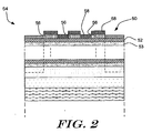
- Figure 2 is a schematic cross-sectional side view of a planar, current-guided, GaAs/AlGaAs top surface emitting vertical cavity laser, as in Figure 1, with a top mounted mode control resonant reflector 50.
- the resonant reflector 50 includes a patterned first material layer 56 that is positioned on top of the top mirror layer 52 of VCSEL 54.
- a second material layer 58 is provided over the patterned first material layer 56, as shown.
- the first material layer 56 preferably has a refractive index that is greater than the refractive index of the second material layer 58, and the first and second material layers 56 and 58 preferably have a refractive index that is less than the refractive index of the top mirror layer 52 of the optoelectronic device 54.
- the first material layer 56 is SiO 2
- the second material layer 58 is Si 3 N 4 or TiO 2
- the top mirror layer 52 is AlGaAs, although other suitable material systems are contemplated.
- Each layer is preferably an even multiple of one-quarter wavelength ( ⁇ /4) thick.
- this difference in reflectivity can be used to help provide mode control for VCSEL 54.
- the first material layer 56 is provided over the top mirror layer 52.
- the first material layer 56 is patterned, preferably by etching away the first material layer 56 in the region or regions circumscribing the desired optical cavity of the VCSEL 54.
- a second material layer 58 is provided over the first material layer 56.
- the second material layer 58 is preferably provided over both the etched 60 and non-etched regions of the first material layer 56, but may be confined to the non-etched regions if desired. Selected regions, such as regions 62a and 62b of the second material layer 58 may then be removed to provide access to the top mirror layer 52.
- a contact layer 64 may be provided on the exposed regions of the top mirror layer 52. The contact layer 64 may provide electrical contact to the top mirror layer 52.
- a top mirror layer of the optoelectronic device may function as the first material layer 56 discussed above.
- the top mirror layer may be patterned, preferably by etching at least partially into the top mirror layer in the region or regions circumscribing the desired optical cavity of the optoelectronic device.
- the layer 52 below the top mirror layer may function as an etch stop layer.
- a second material layer 58 is provided over the top mirror layer.
- the second material layer is preferably provided over both the etched and non-etched regions of the top mirror layer, but may only be provided over the non-etched regions, if desired.
- the regions labeled 56 in Figures 2-3 should have the same cross-hatch pattern as layer 53, and the refractive index of these regions should be less than the refractive index of layer 52.
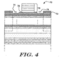
- Figure 4 is a schematic cross-sectional side view of a planar, current-guided, GaAs/AlGaAs top surface emitting vertical cavity laser, as in Figure 1, with another illustrative top mounted mode control resonant reflector 70.
- the resonant reflector 70 is formed by etching down into but not all the way through one or more of the top mirror layers 72 of the optoelectronic device.
- the etched region preferably circumscribes the desired optical cavity of the optoelectronic device, and has a depth that causes a phase shift that reduces the reflectivity of the resonant reflector 70 at the desired operating wavelength, such as a depth that corresponds to an odd multiple of ⁇ /4.
- a cap mirror 76 having one or more additional layers may be provided on selected non-patterned regions 78 of the top mirror layer 72, such as over the desired optical cavity of the optoelectronic device.
- the cap mirror 70 may include one or more periods of a conventional semiconductor DBR mirror, or more preferably, a narrow band dielectric reflection filter.
- a metal layer may be provided on selected regions of the top mirror layer 72. The metal layer may function as a top contact layer.
- a top mirror layer 72 (or some other top layer) is patterned and etched to form one or more etched regions 74.
- the etched regions 74 are preferably formed to circumscribe the desired optical cavity of the optoelectronic device. Also, the etched regions 74 are preferably etched down to a depth that causes a phase shift in the incident light, thereby reducing the reflectivity of the resonant reflector 70 in those regions.
- a cap mirror 76 is formed on the patterned top mirror layer 72.
- the top mirror layer 72 may include one or more semiconductor DBR mirror periods, and/or a narrow band dielectric reflection filter. In either case, and to provide further differentiation in reflectivity, the cap mirror 76 may be etched away except on those areas that correspond to the desired optical cavity of the optoelectronic device. This is shown in Figure 5D.
- the patterned cap mirror 76 may be formed using well known lift-off techniques.
- a contact layer 80 may be provided on the selected regions of the top mirror layer 72. The contact layer 80 may provide electrical contact to the top mirror layer 72.
Landscapes
- Physics & Mathematics (AREA)
- Condensed Matter Physics & Semiconductors (AREA)
- General Physics & Mathematics (AREA)
- Electromagnetism (AREA)
- Optics & Photonics (AREA)
- Semiconductor Lasers (AREA)
- Aerials With Secondary Devices (AREA)
Abstract
Description
- This invention relates to the field of optoelectronic devices, and more particularly to resonant reflectors for optoelectronic devices.
- Conventional semiconductor lasers have found widespread use in modem technology as the light source of choice for various devices, e.g., communication systems, laser printers, compact disc players, and so on. For many of these applications, a semiconductor laser is coupled to a semiconductor receiver (e.g., photodiode) through a fiber optic link or even free space. This configuration may provide a high speed communication path. Lasers that have a single or reduced mode output are particularly suitable for many of these applications because, among other things, they can provide a small spot size.
- A typical edge-emitting semiconductor laser is a double hetorostructure with a narrow bandgap, high refractive index layer surrounded on opposed major surfaces by wide bandgap, low refractive index layers. The low bandgap layer is termed the "active layer", and the bandgap and refractive index differences serve to confine both charge carriers and optical energy to the active layer or region. Opposite ends of the active layer have mirror facets which form the laser cavity. The cladding layers have opposite conductivity types and when current is passed through the structure electrons and holes combine in the active layer to generate light.
- Another type of semiconductor laser which has come to prominence in the last decade are surface emitting lasers. Several types of surface emitting lasers have been developed. One such laser of special promise is termed a "vertical cavity surface emitting laser" (VCSEL). (See, for example, "Surface-emitting microlasers for photonic switching and interchip connections", Optical Engineering, 29, pp. 210-214, March 1990, for a description of this laser). For other examples, note U.S. Patent No. 5,115,442, by Yong H. Lee et al., issued May 19, 1992, and entitled "Top-emitting Surface Emitting Laser Structures" and U.S. Patent No. 5,475,701, issued on December 12, 1995 to Mary K. Hibbs-Brenner, and entitled "Integrated Laser Power Monitor" Also, see "Top-surface-emitting GaAs four-quantum-well lasers emitting at 0.85 µm", Electronics Letters, 26, pp. 710-711, May 24, 1990.)
- Vertical Cavity Surface Emitting Lasers offer numerous performance and potential producibility advantages over conventional edge emitting lasers. These include many benefits associated with their geometry, such as amenability to one- and two-dimensional arrays, wafer-level qualification, and desirable beam characteristics, typically circularly-symmetric low-divergence beams.
- VCSELs typically have an active region with bulk or one or more quantum well layers. On opposite sides of the active region are mirror stacks which are typically formed by interleaved semiconductor layers having properties, such that each layer is typically a quarter wavelength thick at the wavelength (in the medium) of interest thereby forming the mirrors for the laser cavity. There are opposite conductivity type regions on opposite sides of the active region, and the laser is typically turned on and off by varying the current through the active region.
- High-yield, high performance VCSELs have been demonstrated, and exploited in commercialization. Top-surface-emitting A3GaAs-based VCSELs are producible in a manner analogous to semiconductor integrated circuits, and are amenable to low-cost high-volume manufacture and integration with existing electronics technology platforms. Moreover, VCSEL uniformity and reproducibility have been demonstrated using a standard, unmodified commercially available metal organic vapor phase epitaxy (MOVPE) chamber and molecular beam epitaxy (MBE) giving very high device yields.
- VCSELs are expected to provide a performance and cost advantages in fast (e.g., Gbits/s) medium distance (e.g., up to approximately 1000 meters) single or multi-channel data link applications, and numerous optical and/or imaging applications. This results from their inherent geometry, which provides potential low-cost high performance transmitters with flexible and desirable characteristics.
- Most VCSELs of practical dimensions are inherently multi (transverse) mode. Single lowest-order mode VCSELs are favored for coupling into single-mode fibers, and are advantageous for free-space and/or wavelength sensitive systems, and may even be beneficial for use in extending the bandwidth-length product of standard 50 µm and 62.5 µm GRIN multi-mode fiber. However, it has long been known that, although the short optical cavity (2λ) of the VCSEL favors single longitudinal mode emission, the multi-wavelength (10λ) lateral dimensions facilitate multi-transverse mode operation.
- Higher order modes typically have a greater lateral concentration of energy away from the center of the optical or lasing cavity. Thus, the most obvious way to force the laser to oscillate in only a lowest order circularly symmetric mode is to make the lateral dimension of the active area small enough to prevent higher-order modes from reaching threshold. However, this necessitates lateral dimensions of less than about 5 µm for typical VCSELs. Such small areas may result in excessive resistance, and push the limits obtainable from conventional fabrication methodologies. This is particularly true for implantation depths of greater than about 1 µm, where lateral straggle may become a limiting factor. Thus, control of transverse modes remains difficult for VCSEL's of practical dimensions.
- One approach for controlling transverse modes in VCSELs is suggested in U.S. Patent No. 5,903,590 to Hadley et al. Hadley et al. suggest providing a mode control region that extends around the optical cavity of the VCSEL. The mode control region provides a different optical cavity length than the optical cavity length near the center of the VCSEL. This helps reduce the reflectivity in the mode control region. A limitation of Hadley et al. is that the mode control region is formed after the central optical cavity, which adds significant processing steps and increases the cost of the device. In addition, there is an abrupt change in the reflectivity between the mode control region and the optical cavity. This abrupt change can cause diffraction effects, which can reduce the efficiency as well as the quality of the VCSEL.
- The present invention overcomes many of the disadvantages of the prior art by providing a resonant reflector that increases mode control while not requiring a significant amount of additional processing steps. Some resonant reflectors of the present invention also reduce or eliminate abrupt changes in the reflectively across the resonant reflector. This may reduce undesirable diffraction effects that are common in many resonant reflectors, particularly those used for mode control of optoelectronic devices.
- US-A-5940422 discloses a resonant reflect for an optoelectronic device with multiple layers, at least one of which has a patterned region. US-A-6026111 discloses a resonant reflector with optical cavity. WO-A-0045483 discloses a resonant reflector with a mirror region.
- The present invention provides a resonant reflector for an optomelectronic device tuned to a wavelength, the resonant reflector comprises:
- a mirror layer; and
- a first material layer with a first refractive index, the first material layer having one or more patterned regions that extend down through the first material layer and unpatterned regions having a thickness of an even multiple of a quarter of the wavelength;
- wherein a selection of the one or more patterned regions is provided with a second material having a second refractive index, the second material having a thickness of the even multiple of a quarter of the wavelength, such that in the selection of the one or more patterned regions, the second material within the one or more patterned regions is substantially flush with the first material layer, and wherein the mirror layer has a third refractive index and is positioned adjacent the first material layer.
- Preferably, the refractive index is greater than the second refractive index.
- Preferably, the one or more patterned regions reduce the reflectivity of the resonant reflector in those regions.
- Preferably, the one or more patterned regions are positioned to provide control to the optoelectronic device.
- The present invention also provides a resonant reflector for an optoelectronic device tuned to a wavelength, the resonant reflector comprises:
- a mirror layer made of a first material layer with a first refractive index, the first material layer having one or more patterned regions that extend down through the first material layer and unpatterned regions having a thickness of an even multiple of a quarter of the wavelength;
- wherein a selection of the one or more patterned regions is provided with a second material having a second refractive index, the second material having a thickness of the even multiple of a quarter of the wavelength, such that in the selection of the one or more patterned regions, the second material within the one or more patterned regions is substantially flush with the first material layer.
- Preferably, the second material extends outside the one or more patterned regions over unpatterned regions of the first material layer.
- Preferably, the patterned regions of the first material layer comprise etched portions of the first material layer in the region or regions circumscribing a desired optical cavity of the optoelectronic device.
- Preferably, the first and second refractive indices are less than the third refractive index.
- Preferably, the patterned regions of the first material layer comprise etched portions of the first material layer in the region or regions circumscribing a desired optical cavity of the optoelectronic device.
- Preferably, the second material extends outside the one or more patterned regions over unpatterned regions of the first material layer.
- Preferably, the first refractive index is greater than the second refractive index.
- In another illustrative method, a first substantially planar layer of material is provided, followed by a photoresist layer. The photoresist layer is then patterned, preferably forming an island of photoresist. The island of photoresist is then heated, causing it to reflow. This results in a non-planar top surface on the photoresist layer, and preferably one that tapers down toward the first layer of material. Next, the photoresist layer and the first layer of material are etched for a specified period of time. The etchant selectively etches both the photoresist layer and the first layer of material, thereby transferring the shape of the non-planar top surface of the photoresist layer to the first layer of material. A second layer of material is then provided over the first layer of material, if desired. Because the first layer of material assumes the shape of the island of photoresist, and thus has a top surface that tapers down, the second layer of material forms an interface with the first material layer that is non-parallel with the optical axis of the optoelectronic device. As indicated above, this may reduce the diffraction effects caused by abrupt changes in the refraction index of a resonant reflector.
- In yet another illustrative method of the present invention, a first substantially planar layer of material is provided and patterned, resulting in an island of the first layer of material. The island of the first material layer preferably has lateral surfaces that extend up to a top surface defined by top peripheral edges. A photoresist layer is then provided over the patterned first layer of material, including over the lateral surfaces, the top peripheral edges and the top surface. The step from the top surface down along the lateral surfaces causes the photoresist layer to be thinner near the top peripheral edges.
- The photoresist layer and the first layer of material are then etched for a specified period of time. During this etch process, those regions of the first layer of material that are adjacent the thinner regions of the photoresist layer are subject to the etchant for a longer period of time than those regions that are adjacent thicker regions of the photoresist layer. Thus, in the illustrative embodiment, the top peripheral edges of the first layer of material are etched more than those regions away from the top peripheral edges. After the etch process, a second layer of material may be provided over the first layer of material.
- In each of the above embodiments, the top surface of the second layer of material may be planarized by heating the second layer of material to cause it to reflow. Alternatively, or in addition, the top surface of the second layer of material may be planarized using a Chemical Mechanical Polishing (CMP) process. Alternatively, the top surface of the second layer of material may remain substantially non-planar, if desired.
- Other objects of the present invention and many of the attendant advantages of the present invention will be readily appreciated as the same becomes better understood by reference to the following detailed description when considered in connection with the accompanying drawings, in which like reference numerals designate like parts throughout the figures thereof and wherein:
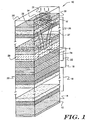
- Figure 1 is a schematic diagram of a planar, current-guided GaAs/A1GaAs top surface emitting vertical cavity laser in accordance with the prior art;
- Figure 2 is a schematic cross-sectional side view of a planar, current-guided, GaAs/A1GaAs top surface emitting vertical cavity laser with a first illustrative resonant reflector for increased mode control in accordance with the present invention;
- Figures 3A-3D are schematic cross-sectional side views showing an illustrative method for making the resonant reflector of Figure 2;
- Figure 4 is a schematic cross-sectional side view of a planar, current-guided, GaAs/A1GaAs top surface emitting vertical cavity laser with a second illustrative resonant reflector for increased mode control in accordance with the present invention;
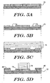
- Figures 5A-5D are schematic cross-sectional side views showing an illustrative method for making the resonant reflector of Figure 4;
- Figure 1 is a schematic illustration of a planar, current-guided, GaAs/A1GaAs top surface emitting
vertical cavity laser 10 in accordance with the prior art. Formed on an n-doped gallium arsenide (GaAs)substrate 14 is an n-contact 12.Substrate 14 is doped with impurities of a first type (i.e., n type). An n-type mirror stack 16 is formed onsubstrate 14. Formed on stack 16 is aspacer 18.Spacer 18 has abottom confinement layer 20 and atop confinement layer 24 surroundingactive region 22. A p-type mirror stack 26 is formed ontop confinement layer 24. A p-metal layer 28 is formed onstack 26. The emission region may have apassivation layer 30. -
Isolation region 29 restricts the area of thecurrent flow 27 through the active region.Region 29 may be formed by deep H+ ion implantation. The diameter "g" may be set to provide the desired active area, and thus the gain aperture of theVCSEL 10. Further, the diameter "g" may be set by the desired resistance of the p-type mirror stack 26, particularly through thenon-conductive region 29. Thus,non-conductive region 29 performs the gain guiding function. The diameter "g" is typically limited by fabrication limitations, such as lateral straggle during the implantation step. -
Spacer 18 may contain a bulk or quantum-well active region disposed between mirror stacks 16 and 26. Quantum-wellactive region 22 may have alternating layers of aluminum gallium arsenide (A1GaAs) barrier layers and GaAs quantum-well layers. InGaAs quantum wells may also be used in the active region, particularly where an emission wavelength (e.g. A = 980 nm) is desired where GaAs is transparent.Stacks 16 and 26 are distributed Bragg reflector (DBR) stacks, and may include periodic layers of doped A1GaAs and aluminum arsenide (A1As). The A1GaAs of stack 16 is doped with the same type of impurity as substrate 14 (e.g., n type), and the AlGaAs ofstack 26 is doped with the other kind of impurity (e.g., p type). - Metal contact layers 12 and 28 are ohmic contacts that allow appropriate electrical biasing of
laser diode 10. Whenlaser diode 10 is forward biased with a more positive voltage oncontact 28 than oncontact 12,active region 22 emits light 31 which passes throughstack 26. - Most VCSELs of practical dimensions are inherently multi (transverse) mode. Single lowest-order mode VCSELs are favored for coupling into single-mode fibers, and are advantageous for free-space and/or wavelength sensitive systems, and may even be beneficial for use in extending the bandwidth-length product of standard 50 µm and 62.5 µm GRIN multi-mode fiber. However, it has long been known that, although the short optical cavity (2 λ) of the VCSEL favors single longitudinal mode emission, the multi-wavelength (10 λ) lateral dimensions facilitate multi-transverse mode operation.
- As indicated above, higher order modes typically have a greater lateral concentration of energy away from the center of the optical or lasing cavity. Thus, the most obvious way to force the laser to oscillate in only a lowest order circularly symmetric mode is to make the lateral dimension "g" of the active area small enough to prevent higher-order modes from reaching threshold. However, this necessitates lateral dimensions of less than about 5 µm for typical VCSELs. Such small areas may result in excessive resistance, and push the limits obtainable from conventional fabrication methodologies. This is particularly true for implantation depths of greater than about 1 µm, where lateral straggle may become a limiting factor. Thus, control of transverse modes remains difficult for VCSEL's of practical dimensions.
- One illustrative approach for controlling transverse modes of an optoelectronic device is shown in Figure 2. Figure 2 is a schematic cross-sectional side view of a planar, current-guided, GaAs/AlGaAs top surface emitting vertical cavity laser, as in Figure 1, with a top mounted mode control
resonant reflector 50. Theresonant reflector 50 includes a patternedfirst material layer 56 that is positioned on top of thetop mirror layer 52 ofVCSEL 54. Asecond material layer 58 is provided over the patternedfirst material layer 56, as shown. - The
first material layer 56 preferably has a refractive index that is greater than the refractive index of thesecond material layer 58, and the first and second material layers 56 and 58 preferably have a refractive index that is less than the refractive index of thetop mirror layer 52 of theoptoelectronic device 54. In one example, thefirst material layer 56 is SiO2, thesecond material layer 58 is Si3N4 or TiO2, and thetop mirror layer 52 is AlGaAs, although other suitable material systems are contemplated. Each layer is preferably an even multiple of one-quarter wavelength (λ /4) thick. This causes a reduction in reflectivity of theresonant reflector 50 in those regions that correspond to the etched regions 60 (see Figure 3B) in thefirst material layer 56, that is, those regions that are filled with thesecond material layer 58. By designing the etched regions to circumscribe the desired optical cavity, this difference in reflectivity can be used to help provide mode control forVCSEL 54. - In forming the
resonant reflector 50, and referring now to Figure 3A, thefirst material layer 56 is provided over thetop mirror layer 52. As shown in Figure 3B, thefirst material layer 56 is patterned, preferably by etching away thefirst material layer 56 in the region or regions circumscribing the desired optical cavity of theVCSEL 54. As shown in Figure 3C, asecond material layer 58 is provided over thefirst material layer 56. Thesecond material layer 58 is preferably provided over both the etched 60 and non-etched regions of thefirst material layer 56, but may be confined to the non-etched regions if desired. Selected regions, such asregions second material layer 58 may then be removed to provide access to thetop mirror layer 52. Then, and as shown in Figure 3D, acontact layer 64 may be provided on the exposed regions of thetop mirror layer 52. Thecontact layer 64 may provide electrical contact to thetop mirror layer 52. - In a related embodiment, a top mirror layer of the optoelectronic device may function as the
first material layer 56 discussed above. Thus, the top mirror layer may be patterned, preferably by etching at least partially into the top mirror layer in the region or regions circumscribing the desired optical cavity of the optoelectronic device. In one embodiment, thelayer 52 below the top mirror layer may function as an etch stop layer. Then, asecond material layer 58 is provided over the top mirror layer. The second material layer is preferably provided over both the etched and non-etched regions of the top mirror layer, but may only be provided over the non-etched regions, if desired. In this embodiment, the regions labeled 56 in Figures 2-3 should have the same cross-hatch pattern aslayer 53, and the refractive index of these regions should be less than the refractive index oflayer 52. - Another illustrative approach for controlling transverse modes of an optoelectronic device is shown in Figure 4. Figure 4 is a schematic cross-sectional side view of a planar, current-guided, GaAs/AlGaAs top surface emitting vertical cavity laser, as in Figure 1, with another illustrative top mounted mode control
resonant reflector 70. In this embodiment, theresonant reflector 70 is formed by etching down into but not all the way through one or more of the top mirror layers 72 of the optoelectronic device. The etched region, generally shown at 74, preferably circumscribes the desired optical cavity of the optoelectronic device, and has a depth that causes a phase shift that reduces the reflectivity of theresonant reflector 70 at the desired operating wavelength, such as a depth that corresponds to an odd multiple of λ/4. To provide further differentiation, acap mirror 76 having one or more additional layers may be provided on selectednon-patterned regions 78 of thetop mirror layer 72, such as over the desired optical cavity of the optoelectronic device. Thecap mirror 70 may include one or more periods of a conventional semiconductor DBR mirror, or more preferably, a narrow band dielectric reflection filter. A metal layer may be provided on selected regions of thetop mirror layer 72. The metal layer may function as a top contact layer. - In forming the
resonant reflector 70, and referring now to Figures 5A-5B, a top mirror layer 72 (or some other top layer) is patterned and etched to form one or moreetched regions 74. Theetched regions 74 are preferably formed to circumscribe the desired optical cavity of the optoelectronic device. Also, the etchedregions 74 are preferably etched down to a depth that causes a phase shift in the incident light, thereby reducing the reflectivity of theresonant reflector 70 in those regions. - Next, and as shown in Figure 5C, a
cap mirror 76 is formed on the patternedtop mirror layer 72. As indicated above, thetop mirror layer 72 may include one or more semiconductor DBR mirror periods, and/or a narrow band dielectric reflection filter. In either case, and to provide further differentiation in reflectivity, thecap mirror 76 may be etched away except on those areas that correspond to the desired optical cavity of the optoelectronic device. This is shown in Figure 5D. Alternatively, the patternedcap mirror 76 may be formed using well known lift-off techniques. Thereafter, acontact layer 80 may be provided on the selected regions of thetop mirror layer 72. Thecontact layer 80 may provide electrical contact to thetop mirror layer 72. - Having thus described the preferred embodiments of the present invention, those of skill in the art will readily appreciate that the teachings found herein may be applied to yet other embodiments within the scope of the claims hereto attached.
Claims (11)
- A resonant reflector (50) for an optomelectronic device (54) tuned to a wavelength, the resonant reflector (50) comprising:a mirror layer, anda first material layer with a first refractive index (56), the first material layer having one or more patterned regions (60) that extend down through the first material layer and unpatterned regions having a thickness of an even multiple of a quarter of the wavelength;wherein a selection of the one or more patterned regions is provided with a second material (58) having a second refractive index, the second material having a thickness of the even multiple of a quarter of the wavelength, such that in the selection of the one or more patterned regions, the second material within the one or more patterned regions is substantially flush with the first material layer, and wherein the mirror layer (52) has a third refractive index and is positioned adjacent the first material layer (56).
- A resonant reflector (50) according to claim 1, wherein the refractive index is greater than the second refractive index.
- A resonant reflector (50) according to claim 1, wherein the one or more patterned regions (60) reduce the reflectivity of the resonant reflector (50) in those regions.
- A resonant reflector according to claim 3, wherein the one or more patterned regions (60) are positioned to provide control to the optoelectronic device (54).
- A resonant reflector (50) for an optoelectronic device (54) tuned to a wavelength, the resonant reflector (50) comprising:a mirror layer made of a first material layer with a first refractive index (56), the first material layer having one or more patterned regions (60) that extend down through the first material layer and unpatterned regions having a thickness of an even multiple of a quarter of the wavelength;wherein a selection of the one or more patterned regions is provided with a second material (58) having a second refractive index, the second material having a thickness of the even multiple of a quarter of the wavelength, such that in the selection of the one or more patterned regions, the second material within the one or more patterned regions is substantially flush with the first material layer.
- The resonant reflector (50) according to claim 1, wherein the second material extends outside the one or more patterned regions over unpatterned regions of the first material layer.
- The resonant reflector (50) according to claim 1, wherein the patterned regions (60) of the first material layer (56) comprise etched portions of the first material layer in the region or regions circumscribing a desired optical cavity of the optoelectronic device.
- The resonant reflector (50) according to claim 1, wherein the first and second refractive indices are less than the third refractive index.
- The resonant reflector (50) according to claim 5, wherein the patterned regions (60) of the first material layer (56) comprise etched portions of the first material layer in the region or regions circumscribing a desired optical cavity of the optoelectronic device.
- The resonant reflector (50) according to claim 5, wherein the second material extends outside the one or more patterned regions over unpatterned regions of the first material layer.
- The resonant reflector (50) according to claim 5, wherein the first refractive index is greater than the second refractive index.
Applications Claiming Priority (3)
| Application Number | Priority Date | Filing Date | Title |
|---|---|---|---|
| US09/751,423 US6727520B2 (en) | 2000-12-29 | 2000-12-29 | Spatially modulated reflector for an optoelectronic device |
| US751423 | 2000-12-29 | ||
| PCT/US2001/050214 WO2002059938A2 (en) | 2000-12-29 | 2001-12-20 | Spatially modulated reflector for an optoelectronic device |
Publications (2)
| Publication Number | Publication Date |
|---|---|
| EP1352455A2 EP1352455A2 (en) | 2003-10-15 |
| EP1352455B1 true EP1352455B1 (en) | 2006-04-19 |
Family
ID=25021913
Family Applications (1)
| Application Number | Title | Priority Date | Filing Date |
|---|---|---|---|
| EP01994427A Expired - Lifetime EP1352455B1 (en) | 2000-12-29 | 2001-12-20 | Spatially modulated reflector for an optoelectronic device |
Country Status (10)
| Country | Link |
|---|---|
| US (4) | US6727520B2 (en) |
| EP (1) | EP1352455B1 (en) |
| JP (1) | JP2004523896A (en) |
| KR (1) | KR20040018249A (en) |
| AT (1) | ATE323959T1 (en) |
| AU (1) | AU2002246819A1 (en) |
| CA (1) | CA2433357A1 (en) |
| DE (1) | DE60118974T2 (en) |
| TW (1) | TW517417B (en) |
| WO (1) | WO2002059938A2 (en) |
Families Citing this family (27)
| Publication number | Priority date | Publication date | Assignee | Title |
|---|---|---|---|---|
| US6727520B2 (en) * | 2000-12-29 | 2004-04-27 | Honeywell International Inc. | Spatially modulated reflector for an optoelectronic device |
| KR100475858B1 (en) * | 2002-04-01 | 2005-03-18 | 주식회사 테라스테이트 | A Vertical Cavity Surface Emitting Lasers |
| TW200505120A (en) * | 2003-07-29 | 2005-02-01 | Copax Photonics Corp | Single transverse mode vertical cavity surface emitting laser device with array structure and method for fabricating the same |
| US7596165B2 (en) * | 2004-08-31 | 2009-09-29 | Finisar Corporation | Distributed Bragg Reflector for optoelectronic device |
| US7920612B2 (en) * | 2004-08-31 | 2011-04-05 | Finisar Corporation | Light emitting semiconductor device having an electrical confinement barrier near the active region |
| US7391799B2 (en) * | 2004-08-31 | 2008-06-24 | Finisar Corporation | Mode selective semiconductor mirror for vertical cavity surface emitting lasers |
| US7829912B2 (en) * | 2006-07-31 | 2010-11-09 | Finisar Corporation | Efficient carrier injection in a semiconductor device |
| JP5376104B2 (en) * | 2005-07-04 | 2013-12-25 | ソニー株式会社 | Surface emitting semiconductor laser |
| JP2007109737A (en) * | 2005-10-11 | 2007-04-26 | Toshiba Corp | Nitride semiconductor laser equipment and its manufacturing method |
| JP2007165501A (en) * | 2005-12-13 | 2007-06-28 | Seiko Epson Corp | Surface-emitting semiconductor laser and its manufacturing method |
| US7883914B2 (en) * | 2006-05-29 | 2011-02-08 | Alight Technologies A/S | Method for fabricating a photonic crystal or photonic bandgap vertical-cavity surface-emitting laser |
| US8031752B1 (en) | 2007-04-16 | 2011-10-04 | Finisar Corporation | VCSEL optimized for high speed data |
| JP4582237B2 (en) * | 2008-01-10 | 2010-11-17 | ソニー株式会社 | Surface emitting semiconductor laser |
| US8077752B2 (en) * | 2008-01-10 | 2011-12-13 | Sony Corporation | Vertical cavity surface emitting laser |
| WO2011046244A1 (en) * | 2009-10-16 | 2011-04-21 | 서울대학교산학협력단 | Iii-nitride surface grating reflector |
| DE102009056387B9 (en) * | 2009-10-30 | 2020-05-07 | Osram Opto Semiconductors Gmbh | Edge-emitting semiconductor laser with a phase structure area for the selection of lateral laser modes |
| JP5532239B2 (en) * | 2009-11-26 | 2014-06-25 | 株式会社リコー | Surface emitting laser element, surface emitting laser array, optical scanning device, and image forming apparatus |
| JP5743520B2 (en) | 2010-12-10 | 2015-07-01 | キヤノン株式会社 | Surface emitting laser and image forming apparatus |
| EP2533380B8 (en) * | 2011-06-06 | 2017-08-30 | Mellanox Technologies, Ltd. | High speed lasing device |
| JP2015008271A (en) * | 2013-05-31 | 2015-01-15 | 株式会社リコー | Surface emitting laser element and atomic oscillator |
| DE102014102360A1 (en) * | 2014-02-24 | 2015-08-27 | Osram Opto Semiconductors Gmbh | laser diode chip |
| CN104297825B (en) * | 2014-10-17 | 2017-04-05 | 中国科学院上海光学精密机械研究所 | Light laser vortex reflecting mirror |
| US9979158B1 (en) * | 2017-01-12 | 2018-05-22 | Technische Universitaet Berlin | Vertical-cavity surface-emitting laser |
| FR3078834B1 (en) * | 2018-03-08 | 2020-03-27 | Commissariat A L'energie Atomique Et Aux Energies Alternatives | LIGHT EMITTING DEVICE COMPRISING AT LEAST ONE VCSEL AND A DIFFUSION LENS |
| JP7258591B2 (en) * | 2019-02-21 | 2023-04-17 | スタンレー電気株式会社 | Vertical cavity light emitting device |
| US11476378B2 (en) * | 2019-05-03 | 2022-10-18 | University Of Central Florida Research Foundation, Inc. | Solar-energy apparatus, methods, and applications |
| WO2021150304A1 (en) * | 2020-01-23 | 2021-07-29 | Yale University | Stacked high contrast gratings and methods of making and using thereof |
Family Cites Families (91)
| Publication number | Priority date | Publication date | Assignee | Title |
|---|---|---|---|---|
| CA1108902A (en) * | 1978-06-15 | 1981-09-15 | R. Ian Macdonald | Wavelength selective optical coupler |
| US4317085A (en) * | 1979-09-12 | 1982-02-23 | Xerox Corporation | Channeled mesa laser |
| US4466094A (en) * | 1982-12-27 | 1984-08-14 | Gte Automatic Electric Inc. | Data capture arrangement for a conference circuit |
| JPS60123084A (en) | 1983-12-08 | 1985-07-01 | Matsushita Electric Ind Co Ltd | Semiconductor light generator |
| US4660207A (en) * | 1984-11-21 | 1987-04-21 | Northern Telecom Limited | Surface-emitting light emitting device |
| US4784722A (en) * | 1985-01-22 | 1988-11-15 | Massachusetts Institute Of Technology | Method forming surface emitting diode laser |
| JPS63126897A (en) * | 1986-05-02 | 1988-05-30 | Yoshitomi Pharmaceut Ind Ltd | Immunosuppressive factor |
| GB2203891A (en) | 1987-04-21 | 1988-10-26 | Plessey Co Plc | Semiconductor diode laser array |
| JPS63318195A (en) * | 1987-06-19 | 1988-12-27 | Agency Of Ind Science & Technol | Transverse buried type surface emitting laser |
| US4885592A (en) * | 1987-12-28 | 1989-12-05 | Kofol J Stephen | Electronically steerable antenna |
| JPH0254981A (en) | 1988-08-20 | 1990-02-23 | Fujitsu Ltd | Surface-emission laser and laser array |
| US4943970A (en) * | 1988-10-24 | 1990-07-24 | General Dynamics Corporation, Electronics Division | Surface emitting laser |
| US4901327A (en) * | 1988-10-24 | 1990-02-13 | General Dynamics Corporation, Electronics Division | Transverse injection surface emitting laser |
| US5256680A (en) * | 1988-11-29 | 1993-10-26 | Warner-Lambert Company | 3,5-di-tertiary-butyl-4-hydroxyphenyl-1,3,4-thiadiazoles, and oxadiazoles and 3,5-di-tertiary-butyl-4-hydroxy-phenyl-1,2,4-thiadazoles, oxadiazoles and triazoles as antiinflammatory agents |
| JPH0675144B2 (en) * | 1989-01-12 | 1994-09-21 | 松下電器産業株式会社 | Optical modulation wave demodulator |
| US4956844A (en) * | 1989-03-17 | 1990-09-11 | Massachusetts Institute Of Technology | Two-dimensional surface-emitting laser array |
| US5031187A (en) * | 1990-02-14 | 1991-07-09 | Bell Communications Research, Inc. | Planar array of vertical-cavity, surface-emitting lasers |
| US5204871A (en) * | 1990-03-29 | 1993-04-20 | Larkins Eric C | Bistable optical laser based on a heterostructure pnpn thyristor |
| US5115442A (en) * | 1990-04-13 | 1992-05-19 | At&T Bell Laboratories | Top-emitting surface emitting laser structures |
| US5034958A (en) * | 1990-04-19 | 1991-07-23 | Bell Communications Research, Inc. | Front-surface emitting diode laser |
| US5052016A (en) * | 1990-05-18 | 1991-09-24 | University Of New Mexico | Resonant-periodic-gain distributed-feedback surface-emitting semiconductor laser |
| US5056098A (en) * | 1990-07-05 | 1991-10-08 | At&T Bell Laboratories | Vertical cavity laser with mirror having controllable reflectivity |
| US5158908A (en) * | 1990-08-31 | 1992-10-27 | At&T Bell Laboratories | Distributed bragg reflectors and devices incorporating same |
| US5253262A (en) * | 1990-10-31 | 1993-10-12 | Kabushiki Kaisha Toshiba | Semiconductor laser device with multi-directional reflector arranged therein |
| US5237581A (en) * | 1990-11-14 | 1993-08-17 | Nec Corporation | Semiconductor multilayer reflector and light emitting device with the same |
| US5216263A (en) * | 1990-11-29 | 1993-06-01 | Xerox Corporation | High density, independently addressable, surface emitting semiconductor laser-light emitting diode arrays |
| US5062115A (en) * | 1990-12-28 | 1991-10-29 | Xerox Corporation | High density, independently addressable, surface emitting semiconductor laser/light emitting diode arrays |
| US5140605A (en) * | 1991-06-27 | 1992-08-18 | Xerox Corporation | Thermally stabilized diode laser structure |
| US5216680A (en) * | 1991-07-11 | 1993-06-01 | Board Of Regents, The University Of Texas System | Optical guided-mode resonance filter |
| US5258990A (en) * | 1991-11-07 | 1993-11-02 | The United States Of America As Represented By The Secretary Of The United States Department Of Energy | Visible light surface emitting semiconductor laser |
| US5404373A (en) * | 1991-11-08 | 1995-04-04 | University Of New Mexico | Electro-optical device |
| US5258316A (en) * | 1992-03-26 | 1993-11-02 | Motorola, Inc. | Patterened mirror vertical cavity surface emitting laser |
| US5325386A (en) * | 1992-04-21 | 1994-06-28 | Bandgap Technology Corporation | Vertical-cavity surface emitting laser assay display system |
| JP3206097B2 (en) | 1992-04-22 | 2001-09-04 | セイコーエプソン株式会社 | Surface emitting semiconductor laser |
| US5245622A (en) * | 1992-05-07 | 1993-09-14 | Bandgap Technology Corporation | Vertical-cavity surface-emitting lasers with intra-cavity structures |
| US5285466A (en) * | 1992-05-20 | 1994-02-08 | Wisconsin Alumni Research Foundation | Feedback mechanism for vertical cavity surface emitting lasers |
| US5293392A (en) * | 1992-07-31 | 1994-03-08 | Motorola, Inc. | Top emitting VCSEL with etch stop layer |
| US5317587A (en) * | 1992-08-06 | 1994-05-31 | Motorola, Inc. | VCSEL with separate control of current distribution and optical mode |
| JPH0669585A (en) * | 1992-08-12 | 1994-03-11 | Fujitsu Ltd | Surface emitting semiconductor laser and its manufacture |
| US5363397A (en) * | 1992-10-29 | 1994-11-08 | Internatioal Business Machines Corporation | Integrated short cavity laser with bragg mirrors |
| US5428634A (en) * | 1992-11-05 | 1995-06-27 | The United States Of America As Represented By The United States Department Of Energy | Visible light emitting vertical cavity surface emitting lasers |
| DE4240706A1 (en) | 1992-12-03 | 1994-06-09 | Siemens Ag | Surface emitting laser diode |
| US5331654A (en) * | 1993-03-05 | 1994-07-19 | Photonics Research Incorporated | Polarized surface-emitting laser |
| US5416044A (en) * | 1993-03-12 | 1995-05-16 | Matsushita Electric Industrial Co., Ltd. | Method for producing a surface-emitting laser |
| US5351256A (en) * | 1993-04-28 | 1994-09-27 | The United States Of America As Represented By The United States Department Of Energy | Electrically injected visible vertical cavity surface emitting laser diodes |
| US5359618A (en) * | 1993-06-01 | 1994-10-25 | Motorola, Inc. | High efficiency VCSEL and method of fabrication |
| US5359447A (en) * | 1993-06-25 | 1994-10-25 | Hewlett-Packard Company | Optical communication with vertical-cavity surface-emitting laser operating in multiple transverse modes |
| US5446754A (en) * | 1993-11-05 | 1995-08-29 | Photonics Research Incorporated | Phased array semiconductor laser |
| US5475701A (en) * | 1993-12-29 | 1995-12-12 | Honeywell Inc. | Integrated laser power monitor |
| US5474701A (en) * | 1994-01-21 | 1995-12-12 | Buckman Laboratories International, Inc. | Enzymes for recreational water |
| KR0132018B1 (en) * | 1994-01-27 | 1998-04-14 | 김만제 | Circle grating surface emitting laser diode |
| JP3611593B2 (en) * | 1994-02-14 | 2005-01-19 | 日本オプネクスト株式会社 | Method for fabricating semiconductor optical device |
| US5513202A (en) * | 1994-02-25 | 1996-04-30 | Matsushita Electric Industrial Co., Ltd. | Vertical-cavity surface-emitting semiconductor laser |
| US5606572A (en) * | 1994-03-24 | 1997-02-25 | Vixel Corporation | Integration of laser with photodiode for feedback control |
| US5557626A (en) * | 1994-06-15 | 1996-09-17 | Motorola | Patterned mirror VCSEL with adjustable selective etch region |
| US5778018A (en) * | 1994-10-13 | 1998-07-07 | Nec Corporation | VCSELs (vertical-cavity surface emitting lasers) and VCSEL-based devices |
| GB2295270A (en) | 1994-11-14 | 1996-05-22 | Sharp Kk | Surface-emitting laser with profiled active region |
| US5530715A (en) * | 1994-11-29 | 1996-06-25 | Motorola, Inc. | Vertical cavity surface emitting laser having continuous grading |
| US5568499A (en) * | 1995-04-07 | 1996-10-22 | Sandia Corporation | Optical device with low electrical and thermal resistance bragg reflectors |
| US5598300A (en) * | 1995-06-05 | 1997-01-28 | Board Of Regents, The University Of Texas System | Efficient bandpass reflection and transmission filters with low sidebands based on guided-mode resonance effects |
| US5574738A (en) * | 1995-06-07 | 1996-11-12 | Honeywell Inc. | Multi-gigahertz frequency-modulated vertical-cavity surface emitting laser |
| US5978401A (en) * | 1995-10-25 | 1999-11-02 | Honeywell Inc. | Monolithic vertical cavity surface emitting laser and resonant cavity photodetector transceiver |
| US5727013A (en) * | 1995-10-27 | 1998-03-10 | Wisconsin Alumni Research Foundation | Single lobe surface emitting complex coupled distributed feedback semiconductor laser |
| FR2741483B1 (en) | 1995-11-21 | 1998-01-02 | Thomson Csf | QUANTUM WELL OPTOELECTRONIC DEVICE |
| GB2311166A (en) * | 1996-03-13 | 1997-09-17 | Sharp Kk | An optoelectronic semiconductor device |
| IL118209A0 (en) * | 1996-05-09 | 1998-02-08 | Yeda Res & Dev | Active electro-optical wavelength-selective mirrors and active electro-optic wavelength-selective filters |
| US5903590A (en) * | 1996-05-20 | 1999-05-11 | Sandia Corporation | Vertical-cavity surface-emitting laser device |
| US5838715A (en) * | 1996-06-20 | 1998-11-17 | Hewlett-Packard Company | High intensity single-mode VCSELs |
| US5940422A (en) * | 1996-06-28 | 1999-08-17 | Honeywell Inc. | Laser with an improved mode control |
| US5774487A (en) * | 1996-10-16 | 1998-06-30 | Honeywell Inc. | Filamented multi-wavelength vertical-cavity surface emitting laser |
| US6078601A (en) * | 1997-03-07 | 2000-06-20 | Smith; David F. | Method for controlling the operation of a laser |
| US6055262A (en) * | 1997-06-11 | 2000-04-25 | Honeywell Inc. | Resonant reflector for improved optoelectronic device performance and enhanced applicability |
| FR2768566B1 (en) | 1997-09-12 | 2000-03-31 | France Telecom | COMPONENTS WITH AN OPTICAL CAVITY DEFINED BY AT LEAST ONE CURVED MIRROR |
| US5966399A (en) * | 1997-10-02 | 1999-10-12 | Motorola, Inc. | Vertical cavity surface emitting laser with integrated diffractive lens and method of fabrication |
| US6026111A (en) * | 1997-10-28 | 2000-02-15 | Motorola, Inc. | Vertical cavity surface emitting laser device having an extended cavity |
| KR100273134B1 (en) * | 1997-11-29 | 2001-01-15 | 정선종 | Single-mode surface-emitting laser |
| US6064683A (en) | 1997-12-12 | 2000-05-16 | Honeywell Inc. | Bandgap isolated light emitter |
| US5979401A (en) * | 1998-08-10 | 1999-11-09 | Ford Global Technologies, Inc. | Internal combustion engine having induction system with aerodynamic charge motion control valve |
| US6185241B1 (en) * | 1998-10-29 | 2001-02-06 | Xerox Corporation | Metal spatial filter to enhance model reflectivity in a vertical cavity surface emitting laser |
| US6144682A (en) * | 1998-10-29 | 2000-11-07 | Xerox Corporation | Spatial absorptive and phase shift filter layer to reduce modal reflectivity for higher order modes in a vertical cavity surface emitting laser |
| GB9901961D0 (en) | 1999-01-29 | 1999-03-17 | Univ Sheffield | Optical device and method of manufacture |
| JP2000330124A (en) | 1999-05-18 | 2000-11-30 | Canon Inc | Production of electrode substrate and liquid crystal device |
| US6411638B1 (en) * | 1999-08-31 | 2002-06-25 | Honeywell Inc. | Coupled cavity anti-guided vertical-cavity surface-emitting laser |
| US6243517B1 (en) * | 1999-11-04 | 2001-06-05 | Sparkolor Corporation | Channel-switched cross-connect |
| US6238944B1 (en) * | 1999-12-21 | 2001-05-29 | Xerox Corporation | Buried heterostructure vertical-cavity surface-emitting laser diodes using impurity induced layer disordering (IILD) via a buried impurity source |
| US6778582B1 (en) * | 2000-03-06 | 2004-08-17 | Novalux, Inc. | Coupled cavity high power semiconductor laser |
| US6782027B2 (en) | 2000-12-29 | 2004-08-24 | Finisar Corporation | Resonant reflector for use with optoelectronic devices |
| US6727520B2 (en) * | 2000-12-29 | 2004-04-27 | Honeywell International Inc. | Spatially modulated reflector for an optoelectronic device |
| US6878958B2 (en) | 2001-03-26 | 2005-04-12 | Gazillion Bits, Inc. | Vertical cavity surface emitting laser with buried dielectric distributed Bragg reflector |
| US6786601B1 (en) * | 2002-09-14 | 2004-09-07 | Shree Kumar Kurup | Method of conveniently thwarting infant amblyopia after cataract removal |
| DE102004022178B4 (en) * | 2004-05-05 | 2008-03-20 | Atmel Germany Gmbh | Method for producing a conductor track on a substrate and component with a conductor track produced in this way |
-
2000
- 2000-12-29 US US09/751,423 patent/US6727520B2/en not_active Expired - Fee Related
-
2001
- 2001-12-20 DE DE60118974T patent/DE60118974T2/en not_active Expired - Lifetime
- 2001-12-20 AU AU2002246819A patent/AU2002246819A1/en not_active Abandoned
- 2001-12-20 EP EP01994427A patent/EP1352455B1/en not_active Expired - Lifetime
- 2001-12-20 CA CA002433357A patent/CA2433357A1/en not_active Abandoned
- 2001-12-20 JP JP2002560170A patent/JP2004523896A/en active Pending
- 2001-12-20 KR KR10-2003-7008908A patent/KR20040018249A/en not_active Application Discontinuation
- 2001-12-20 AT AT01994427T patent/ATE323959T1/en not_active IP Right Cessation
- 2001-12-20 WO PCT/US2001/050214 patent/WO2002059938A2/en not_active Application Discontinuation
- 2001-12-28 TW TW090132789A patent/TW517417B/en not_active IP Right Cessation
-
2004
- 2004-04-07 US US10/819,775 patent/US20040188695A1/en not_active Abandoned
- 2004-04-07 US US10/819,654 patent/US7266135B2/en not_active Expired - Fee Related
-
2007
- 2007-07-19 US US11/776,504 patent/US7760786B2/en not_active Expired - Lifetime
Also Published As
| Publication number | Publication date |
|---|---|
| US20040188695A1 (en) | 2004-09-30 |
| WO2002059938A3 (en) | 2003-07-31 |
| JP2004523896A (en) | 2004-08-05 |
| DE60118974D1 (en) | 2006-05-24 |
| US20020085610A1 (en) | 2002-07-04 |
| US20080037606A1 (en) | 2008-02-14 |
| AU2002246819A1 (en) | 2002-08-06 |
| TW517417B (en) | 2003-01-11 |
| US7760786B2 (en) | 2010-07-20 |
| US6727520B2 (en) | 2004-04-27 |
| US7266135B2 (en) | 2007-09-04 |
| US20040191941A1 (en) | 2004-09-30 |
| DE60118974T2 (en) | 2007-01-04 |
| CA2433357A1 (en) | 2002-08-01 |
| WO2002059938A2 (en) | 2002-08-01 |
| KR20040018249A (en) | 2004-03-02 |
| EP1352455A2 (en) | 2003-10-15 |
| ATE323959T1 (en) | 2006-05-15 |
Similar Documents
| Publication | Publication Date | Title |
|---|---|---|
| EP1352455B1 (en) | Spatially modulated reflector for an optoelectronic device | |
| US7288421B2 (en) | Method for forming an optoelectronic device having an isolation layer | |
| EP0988671B1 (en) | Resonant reflector for improved optoelectronic device performance and enhanced applicability | |
| EP1208622B1 (en) | Coupled cavity anti-guided vertical cavity surface emitting laser (vcsel) | |
| US6836501B2 (en) | Resonant reflector for increased wavelength and polarization control | |
| US6148016A (en) | Integrated semiconductor lasers and photodetectors | |
| EP1955855B1 (en) | Surface light emitting laser element, surface light emitting laser array provided with it, electro-photographic system and optical communication system | |
| US5903590A (en) | Vertical-cavity surface-emitting laser device | |
| US6144682A (en) | Spatial absorptive and phase shift filter layer to reduce modal reflectivity for higher order modes in a vertical cavity surface emitting laser | |
| US5812577A (en) | Surface-emitting laser | |
| US8599897B2 (en) | Tunable detector | |
| TW202308247A (en) | Reflector for vcsel |
Legal Events
| Date | Code | Title | Description |
|---|---|---|---|
| PUAI | Public reference made under article 153(3) epc to a published international application that has entered the european phase |
Free format text: ORIGINAL CODE: 0009012 |
|
| 17P | Request for examination filed |
Effective date: 20030701 |
|
| AK | Designated contracting states |
Kind code of ref document: A2 Designated state(s): AT BE CH CY DE DK ES FI FR GB GR IE IT LI LU MC NL PT SE TR |
|
| AX | Request for extension of the european patent |
Extension state: AL LT LV MK RO SI |
|
| RIN1 | Information on inventor provided before grant (corrected) |
Inventor name: STRZELECKI, EVA, M. Inventor name: MORGAN, ROBERT, A. |
|
| 17Q | First examination report despatched |
Effective date: 20031124 |
|
| RAP1 | Party data changed (applicant data changed or rights of an application transferred) |
Owner name: FINISAR CORPORATION |
|
| GRAP | Despatch of communication of intention to grant a patent |
Free format text: ORIGINAL CODE: EPIDOSNIGR1 |
|
| GRAS | Grant fee paid |
Free format text: ORIGINAL CODE: EPIDOSNIGR3 |
|
| GRAA | (expected) grant |
Free format text: ORIGINAL CODE: 0009210 |
|
| AK | Designated contracting states |
Kind code of ref document: B1 Designated state(s): AT BE CH CY DE DK ES FI FR GB GR IE IT LI LU MC NL PT SE TR |
|
| PG25 | Lapsed in a contracting state [announced via postgrant information from national office to epo] |
Ref country code: IT Free format text: LAPSE BECAUSE OF FAILURE TO SUBMIT A TRANSLATION OF THE DESCRIPTION OR TO PAY THE FEE WITHIN THE PRESCRIBED TIME-LIMIT;WARNING: LAPSES OF ITALIAN PATENTS WITH EFFECTIVE DATE BEFORE 2007 MAY HAVE OCCURRED AT ANY TIME BEFORE 2007. THE CORRECT EFFECTIVE DATE MAY BE DIFFERENT FROM THE ONE RECORDED. Effective date: 20060419 Ref country code: BE Free format text: LAPSE BECAUSE OF FAILURE TO SUBMIT A TRANSLATION OF THE DESCRIPTION OR TO PAY THE FEE WITHIN THE PRESCRIBED TIME-LIMIT Effective date: 20060419 Ref country code: AT Free format text: LAPSE BECAUSE OF FAILURE TO SUBMIT A TRANSLATION OF THE DESCRIPTION OR TO PAY THE FEE WITHIN THE PRESCRIBED TIME-LIMIT Effective date: 20060419 Ref country code: NL Free format text: LAPSE BECAUSE OF FAILURE TO SUBMIT A TRANSLATION OF THE DESCRIPTION OR TO PAY THE FEE WITHIN THE PRESCRIBED TIME-LIMIT Effective date: 20060419 Ref country code: FI Free format text: LAPSE BECAUSE OF FAILURE TO SUBMIT A TRANSLATION OF THE DESCRIPTION OR TO PAY THE FEE WITHIN THE PRESCRIBED TIME-LIMIT Effective date: 20060419 Ref country code: CH Free format text: LAPSE BECAUSE OF FAILURE TO SUBMIT A TRANSLATION OF THE DESCRIPTION OR TO PAY THE FEE WITHIN THE PRESCRIBED TIME-LIMIT Effective date: 20060419 Ref country code: LI Free format text: LAPSE BECAUSE OF FAILURE TO SUBMIT A TRANSLATION OF THE DESCRIPTION OR TO PAY THE FEE WITHIN THE PRESCRIBED TIME-LIMIT Effective date: 20060419 |
|
| REG | Reference to a national code |
Ref country code: GB Ref legal event code: FG4D |
|
| REF | Corresponds to: |
Ref document number: 60118974 Country of ref document: DE Date of ref document: 20060524 Kind code of ref document: P |
|
| REG | Reference to a national code |
Ref country code: IE Ref legal event code: FG4D |
|
| PG25 | Lapsed in a contracting state [announced via postgrant information from national office to epo] |
Ref country code: DK Free format text: LAPSE BECAUSE OF FAILURE TO SUBMIT A TRANSLATION OF THE DESCRIPTION OR TO PAY THE FEE WITHIN THE PRESCRIBED TIME-LIMIT Effective date: 20060719 Ref country code: SE Free format text: LAPSE BECAUSE OF FAILURE TO SUBMIT A TRANSLATION OF THE DESCRIPTION OR TO PAY THE FEE WITHIN THE PRESCRIBED TIME-LIMIT Effective date: 20060719 |
|
| PG25 | Lapsed in a contracting state [announced via postgrant information from national office to epo] |
Ref country code: ES Free format text: LAPSE BECAUSE OF FAILURE TO SUBMIT A TRANSLATION OF THE DESCRIPTION OR TO PAY THE FEE WITHIN THE PRESCRIBED TIME-LIMIT Effective date: 20060730 |
|
| PG25 | Lapsed in a contracting state [announced via postgrant information from national office to epo] |
Ref country code: PT Free format text: LAPSE BECAUSE OF FAILURE TO SUBMIT A TRANSLATION OF THE DESCRIPTION OR TO PAY THE FEE WITHIN THE PRESCRIBED TIME-LIMIT Effective date: 20060919 |
|
| NLV1 | Nl: lapsed or annulled due to failure to fulfill the requirements of art. 29p and 29m of the patents act | ||
| REG | Reference to a national code |
Ref country code: CH Ref legal event code: PL |
|
| ET | Fr: translation filed | ||
| PG25 | Lapsed in a contracting state [announced via postgrant information from national office to epo] |
Ref country code: IE Free format text: LAPSE BECAUSE OF NON-PAYMENT OF DUE FEES Effective date: 20061220 |
|
| PG25 | Lapsed in a contracting state [announced via postgrant information from national office to epo] |
Ref country code: MC Free format text: LAPSE BECAUSE OF NON-PAYMENT OF DUE FEES Effective date: 20061231 |
|
| PLBE | No opposition filed within time limit |
Free format text: ORIGINAL CODE: 0009261 |
|
| STAA | Information on the status of an ep patent application or granted ep patent |
Free format text: STATUS: NO OPPOSITION FILED WITHIN TIME LIMIT |
|
| 26N | No opposition filed |
Effective date: 20070122 |
|
| PG25 | Lapsed in a contracting state [announced via postgrant information from national office to epo] |
Ref country code: GR Free format text: LAPSE BECAUSE OF FAILURE TO SUBMIT A TRANSLATION OF THE DESCRIPTION OR TO PAY THE FEE WITHIN THE PRESCRIBED TIME-LIMIT Effective date: 20060720 |
|
| PG25 | Lapsed in a contracting state [announced via postgrant information from national office to epo] |
Ref country code: TR Free format text: LAPSE BECAUSE OF FAILURE TO SUBMIT A TRANSLATION OF THE DESCRIPTION OR TO PAY THE FEE WITHIN THE PRESCRIBED TIME-LIMIT Effective date: 20060419 Ref country code: LU Free format text: LAPSE BECAUSE OF NON-PAYMENT OF DUE FEES Effective date: 20061220 |
|
| PG25 | Lapsed in a contracting state [announced via postgrant information from national office to epo] |
Ref country code: CY Free format text: LAPSE BECAUSE OF FAILURE TO SUBMIT A TRANSLATION OF THE DESCRIPTION OR TO PAY THE FEE WITHIN THE PRESCRIBED TIME-LIMIT Effective date: 20060419 |
|
| PGFP | Annual fee paid to national office [announced via postgrant information from national office to epo] |
Ref country code: GB Payment date: 20141229 Year of fee payment: 14 |
|
| PGFP | Annual fee paid to national office [announced via postgrant information from national office to epo] |
Ref country code: FR Payment date: 20141217 Year of fee payment: 14 |
|
| PGFP | Annual fee paid to national office [announced via postgrant information from national office to epo] |
Ref country code: DE Payment date: 20141230 Year of fee payment: 14 |
|
| REG | Reference to a national code |
Ref country code: DE Ref legal event code: R119 Ref document number: 60118974 Country of ref document: DE |
|
| GBPC | Gb: european patent ceased through non-payment of renewal fee |
Effective date: 20151220 |
|
| REG | Reference to a national code |
Ref country code: FR Ref legal event code: ST Effective date: 20160831 |
|
| PG25 | Lapsed in a contracting state [announced via postgrant information from national office to epo] |
Ref country code: DE Free format text: LAPSE BECAUSE OF NON-PAYMENT OF DUE FEES Effective date: 20160701 Ref country code: GB Free format text: LAPSE BECAUSE OF NON-PAYMENT OF DUE FEES Effective date: 20151220 |
|
| PG25 | Lapsed in a contracting state [announced via postgrant information from national office to epo] |
Ref country code: FR Free format text: LAPSE BECAUSE OF NON-PAYMENT OF DUE FEES Effective date: 20151231 |