EP1365458A1 - Barrier layer for an article and method of making said barrier layer by expanding thermal plasma - Google Patents
Barrier layer for an article and method of making said barrier layer by expanding thermal plasma Download PDFInfo
- Publication number
- EP1365458A1 EP1365458A1 EP20030253239 EP03253239A EP1365458A1 EP 1365458 A1 EP1365458 A1 EP 1365458A1 EP 20030253239 EP20030253239 EP 20030253239 EP 03253239 A EP03253239 A EP 03253239A EP 1365458 A1 EP1365458 A1 EP 1365458A1
- Authority
- EP
- European Patent Office
- Prior art keywords
- barrier layer
- substrate
- metal
- reagent
- layer
- Prior art date
- Legal status (The legal status is an assumption and is not a legal conclusion. Google has not performed a legal analysis and makes no representation as to the accuracy of the status listed.)
- Withdrawn
Links
- 230000004888 barrier function Effects 0.000 title claims abstract description 190
- 238000004519 manufacturing process Methods 0.000 title description 2
- 239000000758 substrate Substances 0.000 claims abstract description 180
- 238000000151 deposition Methods 0.000 claims abstract description 122
- 239000001301 oxygen Substances 0.000 claims abstract description 88
- 229910052760 oxygen Inorganic materials 0.000 claims abstract description 88
- QVGXLLKOCUKJST-UHFFFAOYSA-N atomic oxygen Chemical compound [O] QVGXLLKOCUKJST-UHFFFAOYSA-N 0.000 claims abstract description 87
- 238000000034 method Methods 0.000 claims abstract description 75
- 230000005540 biological transmission Effects 0.000 claims abstract description 68
- 229910052751 metal Inorganic materials 0.000 claims description 120
- 239000002184 metal Substances 0.000 claims description 120
- 239000003153 chemical reaction reagent Substances 0.000 claims description 77
- 230000008021 deposition Effects 0.000 claims description 75
- 239000002243 precursor Substances 0.000 claims description 54
- 229910052782 aluminium Inorganic materials 0.000 claims description 46
- XAGFODPZIPBFFR-UHFFFAOYSA-N aluminium Chemical compound [Al] XAGFODPZIPBFFR-UHFFFAOYSA-N 0.000 claims description 46
- 150000004767 nitrides Chemical class 0.000 claims description 44
- ATJFFYVFTNAWJD-UHFFFAOYSA-N Tin Chemical compound [Sn] ATJFFYVFTNAWJD-UHFFFAOYSA-N 0.000 claims description 42
- 229910052718 tin Inorganic materials 0.000 claims description 42
- HCHKCACWOHOZIP-UHFFFAOYSA-N Zinc Chemical compound [Zn] HCHKCACWOHOZIP-UHFFFAOYSA-N 0.000 claims description 40
- 229910052725 zinc Inorganic materials 0.000 claims description 40
- 239000011701 zinc Substances 0.000 claims description 40
- XUIMIQQOPSSXEZ-UHFFFAOYSA-N Silicon Chemical compound [Si] XUIMIQQOPSSXEZ-UHFFFAOYSA-N 0.000 claims description 39
- 229910052710 silicon Inorganic materials 0.000 claims description 39
- 239000010703 silicon Substances 0.000 claims description 39
- XLYOFNOQVPJJNP-UHFFFAOYSA-N water Chemical compound O XLYOFNOQVPJJNP-UHFFFAOYSA-N 0.000 claims description 38
- 229910044991 metal oxide Inorganic materials 0.000 claims description 35
- 150000004706 metal oxides Chemical class 0.000 claims description 35
- 229910052738 indium Inorganic materials 0.000 claims description 34
- APFVFJFRJDLVQX-UHFFFAOYSA-N indium atom Chemical compound [In] APFVFJFRJDLVQX-UHFFFAOYSA-N 0.000 claims description 34
- QGZKDVFQNNGYKY-UHFFFAOYSA-N Ammonia Chemical compound N QGZKDVFQNNGYKY-UHFFFAOYSA-N 0.000 claims description 30
- 229910052723 transition metal Inorganic materials 0.000 claims description 29
- 150000003624 transition metals Chemical class 0.000 claims description 29
- IJGRMHOSHXDMSA-UHFFFAOYSA-N Atomic nitrogen Chemical compound N#N IJGRMHOSHXDMSA-UHFFFAOYSA-N 0.000 claims description 26
- 229910021529 ammonia Inorganic materials 0.000 claims description 15
- 229910010272 inorganic material Inorganic materials 0.000 claims description 14
- 239000011147 inorganic material Substances 0.000 claims description 14
- 229910052757 nitrogen Inorganic materials 0.000 claims description 13
- 229910001868 water Inorganic materials 0.000 claims description 9
- 230000001737 promoting effect Effects 0.000 claims description 3
- 239000004973 liquid crystal related substance Substances 0.000 abstract description 17
- 238000005299 abrasion Methods 0.000 abstract description 7
- 239000010410 layer Substances 0.000 description 274
- 210000002381 plasma Anatomy 0.000 description 104
- 239000007789 gas Substances 0.000 description 26
- RTAQQCXQSZGOHL-UHFFFAOYSA-N Titanium Chemical compound [Ti] RTAQQCXQSZGOHL-UHFFFAOYSA-N 0.000 description 19
- 229910052719 titanium Inorganic materials 0.000 description 19
- 239000010936 titanium Substances 0.000 description 19
- 239000000376 reactant Substances 0.000 description 18
- 239000000463 material Substances 0.000 description 16
- XKRFYHLGVUSROY-UHFFFAOYSA-N Argon Chemical compound [Ar] XKRFYHLGVUSROY-UHFFFAOYSA-N 0.000 description 14
- VYPSYNLAJGMNEJ-UHFFFAOYSA-N Silicium dioxide Chemical compound O=[Si]=O VYPSYNLAJGMNEJ-UHFFFAOYSA-N 0.000 description 14
- PPBRXRYQALVLMV-UHFFFAOYSA-N Styrene Chemical compound C=CC1=CC=CC=C1 PPBRXRYQALVLMV-UHFFFAOYSA-N 0.000 description 14
- MCMNRKCIXSYSNV-UHFFFAOYSA-N Zirconium dioxide Chemical compound O=[Zr]=O MCMNRKCIXSYSNV-UHFFFAOYSA-N 0.000 description 14
- 239000011521 glass Substances 0.000 description 14
- BASFCYQUMIYNBI-UHFFFAOYSA-N platinum Chemical compound [Pt] BASFCYQUMIYNBI-UHFFFAOYSA-N 0.000 description 14
- 229910052793 cadmium Inorganic materials 0.000 description 13
- -1 polyethylene Polymers 0.000 description 13
- 229910010293 ceramic material Inorganic materials 0.000 description 12
- 229910052581 Si3N4 Inorganic materials 0.000 description 10
- HQVNEWCFYHHQES-UHFFFAOYSA-N silicon nitride Chemical compound N12[Si]34N5[Si]62N3[Si]51N64 HQVNEWCFYHHQES-UHFFFAOYSA-N 0.000 description 10
- BLRPTPMANUNPDV-UHFFFAOYSA-N Silane Chemical compound [SiH4] BLRPTPMANUNPDV-UHFFFAOYSA-N 0.000 description 9
- 230000005525 hole transport Effects 0.000 description 9
- GYHNNYVSQQEPJS-UHFFFAOYSA-N Gallium Chemical compound [Ga] GYHNNYVSQQEPJS-UHFFFAOYSA-N 0.000 description 8
- BDOSMKKIYDKNTQ-UHFFFAOYSA-N cadmium atom Chemical compound [Cd] BDOSMKKIYDKNTQ-UHFFFAOYSA-N 0.000 description 8
- 229910052733 gallium Inorganic materials 0.000 description 8
- 150000002894 organic compounds Chemical class 0.000 description 8
- 239000011368 organic material Substances 0.000 description 8
- 229910000077 silane Inorganic materials 0.000 description 8
- VXUYXOFXAQZZMF-UHFFFAOYSA-N titanium(IV) isopropoxide Chemical compound CC(C)O[Ti](OC(C)C)(OC(C)C)OC(C)C VXUYXOFXAQZZMF-UHFFFAOYSA-N 0.000 description 8
- NIXOWILDQLNWCW-UHFFFAOYSA-M Acrylate Chemical compound [O-]C(=O)C=C NIXOWILDQLNWCW-UHFFFAOYSA-M 0.000 description 7
- NLHHRLWOUZZQLW-UHFFFAOYSA-N Acrylonitrile Chemical compound C=CC#N NLHHRLWOUZZQLW-UHFFFAOYSA-N 0.000 description 7
- 229910052580 B4C Inorganic materials 0.000 description 7
- 229910052582 BN Inorganic materials 0.000 description 7
- ZOXJGFHDIHLPTG-UHFFFAOYSA-N Boron Chemical compound [B] ZOXJGFHDIHLPTG-UHFFFAOYSA-N 0.000 description 7
- PZNSFCLAULLKQX-UHFFFAOYSA-N Boron nitride Chemical compound N#B PZNSFCLAULLKQX-UHFFFAOYSA-N 0.000 description 7
- VYZAMTAEIAYCRO-UHFFFAOYSA-N Chromium Chemical compound [Cr] VYZAMTAEIAYCRO-UHFFFAOYSA-N 0.000 description 7
- ZOKXTWBITQBERF-UHFFFAOYSA-N Molybdenum Chemical compound [Mo] ZOKXTWBITQBERF-UHFFFAOYSA-N 0.000 description 7
- CTQNGGLPUBDAKN-UHFFFAOYSA-N O-Xylene Chemical compound CC1=CC=CC=C1C CTQNGGLPUBDAKN-UHFFFAOYSA-N 0.000 description 7
- GWEVSGVZZGPLCZ-UHFFFAOYSA-N Titan oxide Chemical compound O=[Ti]=O GWEVSGVZZGPLCZ-UHFFFAOYSA-N 0.000 description 7
- QCWXUUIWCKQGHC-UHFFFAOYSA-N Zirconium Chemical compound [Zr] QCWXUUIWCKQGHC-UHFFFAOYSA-N 0.000 description 7
- PNEYBMLMFCGWSK-UHFFFAOYSA-N aluminium oxide Inorganic materials [O-2].[O-2].[O-2].[Al+3].[Al+3] PNEYBMLMFCGWSK-UHFFFAOYSA-N 0.000 description 7
- 229910003481 amorphous carbon Inorganic materials 0.000 description 7
- 229910052786 argon Inorganic materials 0.000 description 7
- 229910052796 boron Inorganic materials 0.000 description 7
- INAHAJYZKVIDIZ-UHFFFAOYSA-N boron carbide Chemical compound B12B3B4C32B41 INAHAJYZKVIDIZ-UHFFFAOYSA-N 0.000 description 7
- 229910052804 chromium Inorganic materials 0.000 description 7
- 239000011651 chromium Substances 0.000 description 7
- 238000000576 coating method Methods 0.000 description 7
- 150000002118 epoxides Chemical class 0.000 description 7
- 229910052732 germanium Inorganic materials 0.000 description 7
- GNPVGFCGXDBREM-UHFFFAOYSA-N germanium atom Chemical compound [Ge] GNPVGFCGXDBREM-UHFFFAOYSA-N 0.000 description 7
- 229910052735 hafnium Inorganic materials 0.000 description 7
- VBJZVLUMGGDVMO-UHFFFAOYSA-N hafnium atom Chemical compound [Hf] VBJZVLUMGGDVMO-UHFFFAOYSA-N 0.000 description 7
- 229910052750 molybdenum Inorganic materials 0.000 description 7
- 239000011733 molybdenum Substances 0.000 description 7
- 229910052697 platinum Inorganic materials 0.000 description 7
- 239000004417 polycarbonate Substances 0.000 description 7
- 229920000515 polycarbonate Polymers 0.000 description 7
- 229920000642 polymer Polymers 0.000 description 7
- 239000000377 silicon dioxide Substances 0.000 description 7
- 229910052715 tantalum Inorganic materials 0.000 description 7
- GUVRBAGPIYLISA-UHFFFAOYSA-N tantalum atom Chemical compound [Ta] GUVRBAGPIYLISA-UHFFFAOYSA-N 0.000 description 7
- OGIDPMRJRNCKJF-UHFFFAOYSA-N titanium oxide Inorganic materials [Ti]=O OGIDPMRJRNCKJF-UHFFFAOYSA-N 0.000 description 7
- WFKWXMTUELFFGS-UHFFFAOYSA-N tungsten Chemical compound [W] WFKWXMTUELFFGS-UHFFFAOYSA-N 0.000 description 7
- 229910052721 tungsten Inorganic materials 0.000 description 7
- 239000010937 tungsten Substances 0.000 description 7
- 229910052720 vanadium Inorganic materials 0.000 description 7
- LEONUFNNVUYDNQ-UHFFFAOYSA-N vanadium atom Chemical compound [V] LEONUFNNVUYDNQ-UHFFFAOYSA-N 0.000 description 7
- 239000008096 xylene Substances 0.000 description 7
- 229910052726 zirconium Inorganic materials 0.000 description 7
- XLOMVQKBTHCTTD-UHFFFAOYSA-N Zinc monoxide Chemical compound [Zn]=O XLOMVQKBTHCTTD-UHFFFAOYSA-N 0.000 description 6
- 238000006243 chemical reaction Methods 0.000 description 6
- KPUWHANPEXNPJT-UHFFFAOYSA-N disiloxane Chemical class [SiH3]O[SiH3] KPUWHANPEXNPJT-UHFFFAOYSA-N 0.000 description 6
- 239000001257 hydrogen Substances 0.000 description 6
- 229910052739 hydrogen Inorganic materials 0.000 description 6
- 125000004435 hydrogen atom Chemical class [H]* 0.000 description 6
- 229910001507 metal halide Inorganic materials 0.000 description 6
- 150000005309 metal halides Chemical class 0.000 description 6
- 229920001296 polysiloxane Polymers 0.000 description 6
- 239000004695 Polyether sulfone Substances 0.000 description 5
- 239000004698 Polyethylene Substances 0.000 description 5
- 239000004642 Polyimide Substances 0.000 description 5
- BQCADISMDOOEFD-UHFFFAOYSA-N Silver Chemical compound [Ag] BQCADISMDOOEFD-UHFFFAOYSA-N 0.000 description 5
- 229910000831 Steel Inorganic materials 0.000 description 5
- 239000011248 coating agent Substances 0.000 description 5
- 239000011152 fibreglass Substances 0.000 description 5
- AMGQUBHHOARCQH-UHFFFAOYSA-N indium;oxotin Chemical compound [In].[Sn]=O AMGQUBHHOARCQH-UHFFFAOYSA-N 0.000 description 5
- 150000002500 ions Chemical class 0.000 description 5
- 239000000178 monomer Substances 0.000 description 5
- 229920000058 polyacrylate Polymers 0.000 description 5
- 229920006393 polyether sulfone Polymers 0.000 description 5
- 229920000573 polyethylene Polymers 0.000 description 5
- 229920001721 polyimide Polymers 0.000 description 5
- 229910052709 silver Inorganic materials 0.000 description 5
- 239000004332 silver Substances 0.000 description 5
- 229940071182 stannate Drugs 0.000 description 5
- 239000010959 steel Substances 0.000 description 5
- 239000005046 Chlorosilane Substances 0.000 description 4
- KOPOQZFJUQMUML-UHFFFAOYSA-N chlorosilane Chemical class Cl[SiH3] KOPOQZFJUQMUML-UHFFFAOYSA-N 0.000 description 4
- 230000007613 environmental effect Effects 0.000 description 4
- 229920000620 organic polymer Polymers 0.000 description 4
- 238000000623 plasma-assisted chemical vapour deposition Methods 0.000 description 4
- 229920000636 poly(norbornene) polymer Polymers 0.000 description 4
- FZHAPNGMFPVSLP-UHFFFAOYSA-N silanamine Chemical class [SiH3]N FZHAPNGMFPVSLP-UHFFFAOYSA-N 0.000 description 4
- SMZOGRDCAXLAAR-UHFFFAOYSA-N aluminium isopropoxide Chemical compound [Al+3].CC(C)[O-].CC(C)[O-].CC(C)[O-] SMZOGRDCAXLAAR-UHFFFAOYSA-N 0.000 description 3
- 229910000420 cerium oxide Inorganic materials 0.000 description 3
- HQWPLXHWEZZGKY-UHFFFAOYSA-N diethylzinc Chemical compound CC[Zn]CC HQWPLXHWEZZGKY-UHFFFAOYSA-N 0.000 description 3
- AXAZMDOAUQTMOW-UHFFFAOYSA-N dimethylzinc Chemical compound C[Zn]C AXAZMDOAUQTMOW-UHFFFAOYSA-N 0.000 description 3
- PZPGRFITIJYNEJ-UHFFFAOYSA-N disilane Chemical compound [SiH3][SiH3] PZPGRFITIJYNEJ-UHFFFAOYSA-N 0.000 description 3
- 239000001307 helium Substances 0.000 description 3
- 229910052734 helium Inorganic materials 0.000 description 3
- SWQJXJOGLNCZEY-UHFFFAOYSA-N helium atom Chemical compound [He] SWQJXJOGLNCZEY-UHFFFAOYSA-N 0.000 description 3
- BMMGVYCKOGBVEV-UHFFFAOYSA-N oxo(oxoceriooxy)cerium Chemical compound [Ce]=O.O=[Ce]=O BMMGVYCKOGBVEV-UHFFFAOYSA-N 0.000 description 3
- 229920006289 polycarbonate film Polymers 0.000 description 3
- OVZUSPADPSOQQN-UHFFFAOYSA-N tri(propan-2-yloxy)indigane Chemical compound [In+3].CC(C)[O-].CC(C)[O-].CC(C)[O-] OVZUSPADPSOQQN-UHFFFAOYSA-N 0.000 description 3
- SSEICBQSWNBGQZ-UHFFFAOYSA-N tris[(2-methylpropan-2-yl)oxy]indigane Chemical compound CC(C)(C)O[In](OC(C)(C)C)OC(C)(C)C SSEICBQSWNBGQZ-UHFFFAOYSA-N 0.000 description 3
- 239000011787 zinc oxide Substances 0.000 description 3
- ATUOYWHBWRKTHZ-UHFFFAOYSA-N Propane Chemical compound CCC ATUOYWHBWRKTHZ-UHFFFAOYSA-N 0.000 description 2
- 238000005229 chemical vapour deposition Methods 0.000 description 2
- 239000007772 electrode material Substances 0.000 description 2
- 239000012530 fluid Substances 0.000 description 2
- 238000007735 ion beam assisted deposition Methods 0.000 description 2
- 229910001510 metal chloride Inorganic materials 0.000 description 2
- 239000000203 mixture Substances 0.000 description 2
- 230000006798 recombination Effects 0.000 description 2
- 238000005215 recombination Methods 0.000 description 2
- 239000004065 semiconductor Substances 0.000 description 2
- 239000002356 single layer Substances 0.000 description 2
- FYYHWMGAXLPEAU-UHFFFAOYSA-N Magnesium Chemical compound [Mg] FYYHWMGAXLPEAU-UHFFFAOYSA-N 0.000 description 1
- 230000006978 adaptation Effects 0.000 description 1
- 230000002411 adverse Effects 0.000 description 1
- HSFWRNGVRCDJHI-UHFFFAOYSA-N alpha-acetylene Natural products C#C HSFWRNGVRCDJHI-UHFFFAOYSA-N 0.000 description 1
- ZOZLFBZFMZKVFW-UHFFFAOYSA-N aluminum;zinc Chemical compound [Al+3].[Zn+2] ZOZLFBZFMZKVFW-UHFFFAOYSA-N 0.000 description 1
- 239000001273 butane Substances 0.000 description 1
- 239000000919 ceramic Substances 0.000 description 1
- 150000001805 chlorine compounds Chemical class 0.000 description 1
- 238000001816 cooling Methods 0.000 description 1
- 238000000354 decomposition reaction Methods 0.000 description 1
- 238000010494 dissociation reaction Methods 0.000 description 1
- 230000005593 dissociations Effects 0.000 description 1
- 238000005538 encapsulation Methods 0.000 description 1
- 125000002534 ethynyl group Chemical group [H]C#C* 0.000 description 1
- 230000008020 evaporation Effects 0.000 description 1
- 238000001704 evaporation Methods 0.000 description 1
- 238000006062 fragmentation reaction Methods 0.000 description 1
- BHEPBYXIRTUNPN-UHFFFAOYSA-N hydridophosphorus(.) (triplet) Chemical compound [PH] BHEPBYXIRTUNPN-UHFFFAOYSA-N 0.000 description 1
- 238000003384 imaging method Methods 0.000 description 1
- 238000009616 inductively coupled plasma Methods 0.000 description 1
- 239000011261 inert gas Substances 0.000 description 1
- 238000002347 injection Methods 0.000 description 1
- 239000007924 injection Substances 0.000 description 1
- 229920000592 inorganic polymer Polymers 0.000 description 1
- 229910052743 krypton Inorganic materials 0.000 description 1
- DNNSSWSSYDEUBZ-UHFFFAOYSA-N krypton atom Chemical compound [Kr] DNNSSWSSYDEUBZ-UHFFFAOYSA-N 0.000 description 1
- 229910052749 magnesium Inorganic materials 0.000 description 1
- 239000011777 magnesium Substances 0.000 description 1
- 238000012986 modification Methods 0.000 description 1
- 230000004048 modification Effects 0.000 description 1
- IJDNQMDRQITEOD-UHFFFAOYSA-N n-butane Chemical compound CCCC IJDNQMDRQITEOD-UHFFFAOYSA-N 0.000 description 1
- OFBQJSOFQDEBGM-UHFFFAOYSA-N n-pentane Natural products CCCCC OFBQJSOFQDEBGM-UHFFFAOYSA-N 0.000 description 1
- 229910052754 neon Inorganic materials 0.000 description 1
- GKAOGPIIYCISHV-UHFFFAOYSA-N neon atom Chemical compound [Ne] GKAOGPIIYCISHV-UHFFFAOYSA-N 0.000 description 1
- 229910052756 noble gas Inorganic materials 0.000 description 1
- 230000000704 physical effect Effects 0.000 description 1
- 230000008569 process Effects 0.000 description 1
- 239000001294 propane Substances 0.000 description 1
- 239000011253 protective coating Substances 0.000 description 1
- 150000004756 silanes Chemical class 0.000 description 1
- 238000004544 sputter deposition Methods 0.000 description 1
- XJDNKRIXUMDJCW-UHFFFAOYSA-J titanium tetrachloride Chemical compound Cl[Ti](Cl)(Cl)Cl XJDNKRIXUMDJCW-UHFFFAOYSA-J 0.000 description 1
- 229910052724 xenon Inorganic materials 0.000 description 1
- FHNFHKCVQCLJFQ-UHFFFAOYSA-N xenon atom Chemical compound [Xe] FHNFHKCVQCLJFQ-UHFFFAOYSA-N 0.000 description 1
Images


Classifications
-
- H—ELECTRICITY
- H01—ELECTRIC ELEMENTS
- H01L—SEMICONDUCTOR DEVICES NOT COVERED BY CLASS H10
- H01L23/00—Details of semiconductor or other solid state devices
- H01L23/564—Details not otherwise provided for, e.g. protection against moisture
-
- C—CHEMISTRY; METALLURGY
- C23—COATING METALLIC MATERIAL; COATING MATERIAL WITH METALLIC MATERIAL; CHEMICAL SURFACE TREATMENT; DIFFUSION TREATMENT OF METALLIC MATERIAL; COATING BY VACUUM EVAPORATION, BY SPUTTERING, BY ION IMPLANTATION OR BY CHEMICAL VAPOUR DEPOSITION, IN GENERAL; INHIBITING CORROSION OF METALLIC MATERIAL OR INCRUSTATION IN GENERAL
- C23C—COATING METALLIC MATERIAL; COATING MATERIAL WITH METALLIC MATERIAL; SURFACE TREATMENT OF METALLIC MATERIAL BY DIFFUSION INTO THE SURFACE, BY CHEMICAL CONVERSION OR SUBSTITUTION; COATING BY VACUUM EVAPORATION, BY SPUTTERING, BY ION IMPLANTATION OR BY CHEMICAL VAPOUR DEPOSITION, IN GENERAL
- C23C16/00—Chemical coating by decomposition of gaseous compounds, without leaving reaction products of surface material in the coating, i.e. chemical vapour deposition [CVD] processes
- C23C16/22—Chemical coating by decomposition of gaseous compounds, without leaving reaction products of surface material in the coating, i.e. chemical vapour deposition [CVD] processes characterised by the deposition of inorganic material, other than metallic material
- C23C16/30—Deposition of compounds, mixtures or solid solutions, e.g. borides, carbides, nitrides
- C23C16/34—Nitrides
- C23C16/345—Silicon nitride
-
- C—CHEMISTRY; METALLURGY
- C23—COATING METALLIC MATERIAL; COATING MATERIAL WITH METALLIC MATERIAL; CHEMICAL SURFACE TREATMENT; DIFFUSION TREATMENT OF METALLIC MATERIAL; COATING BY VACUUM EVAPORATION, BY SPUTTERING, BY ION IMPLANTATION OR BY CHEMICAL VAPOUR DEPOSITION, IN GENERAL; INHIBITING CORROSION OF METALLIC MATERIAL OR INCRUSTATION IN GENERAL
- C23C—COATING METALLIC MATERIAL; COATING MATERIAL WITH METALLIC MATERIAL; SURFACE TREATMENT OF METALLIC MATERIAL BY DIFFUSION INTO THE SURFACE, BY CHEMICAL CONVERSION OR SUBSTITUTION; COATING BY VACUUM EVAPORATION, BY SPUTTERING, BY ION IMPLANTATION OR BY CHEMICAL VAPOUR DEPOSITION, IN GENERAL
- C23C16/00—Chemical coating by decomposition of gaseous compounds, without leaving reaction products of surface material in the coating, i.e. chemical vapour deposition [CVD] processes
- C23C16/44—Chemical coating by decomposition of gaseous compounds, without leaving reaction products of surface material in the coating, i.e. chemical vapour deposition [CVD] processes characterised by the method of coating
- C23C16/50—Chemical coating by decomposition of gaseous compounds, without leaving reaction products of surface material in the coating, i.e. chemical vapour deposition [CVD] processes characterised by the method of coating using electric discharges
- C23C16/513—Chemical coating by decomposition of gaseous compounds, without leaving reaction products of surface material in the coating, i.e. chemical vapour deposition [CVD] processes characterised by the method of coating using electric discharges using plasma jets
-
- H—ELECTRICITY
- H10—SEMICONDUCTOR DEVICES; ELECTRIC SOLID-STATE DEVICES NOT OTHERWISE PROVIDED FOR
- H10K—ORGANIC ELECTRIC SOLID-STATE DEVICES
- H10K50/00—Organic light-emitting devices
- H10K50/80—Constructional details
- H10K50/84—Passivation; Containers; Encapsulations
- H10K50/844—Encapsulations
-
- C—CHEMISTRY; METALLURGY
- C09—DYES; PAINTS; POLISHES; NATURAL RESINS; ADHESIVES; COMPOSITIONS NOT OTHERWISE PROVIDED FOR; APPLICATIONS OF MATERIALS NOT OTHERWISE PROVIDED FOR
- C09K—MATERIALS FOR MISCELLANEOUS APPLICATIONS, NOT PROVIDED FOR ELSEWHERE
- C09K2323/00—Functional layers of liquid crystal optical display excluding electroactive liquid crystal layer characterised by chemical composition
-
- H—ELECTRICITY
- H01—ELECTRIC ELEMENTS
- H01L—SEMICONDUCTOR DEVICES NOT COVERED BY CLASS H10
- H01L2924/00—Indexing scheme for arrangements or methods for connecting or disconnecting semiconductor or solid-state bodies as covered by H01L24/00
- H01L2924/0001—Technical content checked by a classifier
- H01L2924/0002—Not covered by any one of groups H01L24/00, H01L24/00 and H01L2224/00
-
- H—ELECTRICITY
- H01—ELECTRIC ELEMENTS
- H01L—SEMICONDUCTOR DEVICES NOT COVERED BY CLASS H10
- H01L2924/00—Indexing scheme for arrangements or methods for connecting or disconnecting semiconductor or solid-state bodies as covered by H01L24/00
- H01L2924/10—Details of semiconductor or other solid state devices to be connected
- H01L2924/11—Device type
- H01L2924/12—Passive devices, e.g. 2 terminal devices
- H01L2924/1204—Optical Diode
- H01L2924/12044—OLED
-
- Y—GENERAL TAGGING OF NEW TECHNOLOGICAL DEVELOPMENTS; GENERAL TAGGING OF CROSS-SECTIONAL TECHNOLOGIES SPANNING OVER SEVERAL SECTIONS OF THE IPC; TECHNICAL SUBJECTS COVERED BY FORMER USPC CROSS-REFERENCE ART COLLECTIONS [XRACs] AND DIGESTS
- Y02—TECHNOLOGIES OR APPLICATIONS FOR MITIGATION OR ADAPTATION AGAINST CLIMATE CHANGE
- Y02T—CLIMATE CHANGE MITIGATION TECHNOLOGIES RELATED TO TRANSPORTATION
- Y02T50/00—Aeronautics or air transport
- Y02T50/60—Efficient propulsion technologies, e.g. for aircraft
-
- Y—GENERAL TAGGING OF NEW TECHNOLOGICAL DEVELOPMENTS; GENERAL TAGGING OF CROSS-SECTIONAL TECHNOLOGIES SPANNING OVER SEVERAL SECTIONS OF THE IPC; TECHNICAL SUBJECTS COVERED BY FORMER USPC CROSS-REFERENCE ART COLLECTIONS [XRACs] AND DIGESTS
- Y10—TECHNICAL SUBJECTS COVERED BY FORMER USPC
- Y10S—TECHNICAL SUBJECTS COVERED BY FORMER USPC CROSS-REFERENCE ART COLLECTIONS [XRACs] AND DIGESTS
- Y10S428/00—Stock material or miscellaneous articles
- Y10S428/913—Material designed to be responsive to temperature, light, moisture
-
- Y—GENERAL TAGGING OF NEW TECHNOLOGICAL DEVELOPMENTS; GENERAL TAGGING OF CROSS-SECTIONAL TECHNOLOGIES SPANNING OVER SEVERAL SECTIONS OF THE IPC; TECHNICAL SUBJECTS COVERED BY FORMER USPC CROSS-REFERENCE ART COLLECTIONS [XRACs] AND DIGESTS
- Y10—TECHNICAL SUBJECTS COVERED BY FORMER USPC
- Y10T—TECHNICAL SUBJECTS COVERED BY FORMER US CLASSIFICATION
- Y10T428/00—Stock material or miscellaneous articles
- Y10T428/26—Web or sheet containing structurally defined element or component, the element or component having a specified physical dimension
- Y10T428/263—Coating layer not in excess of 5 mils thick or equivalent
- Y10T428/264—Up to 3 mils
- Y10T428/265—1 mil or less
-
- Y—GENERAL TAGGING OF NEW TECHNOLOGICAL DEVELOPMENTS; GENERAL TAGGING OF CROSS-SECTIONAL TECHNOLOGIES SPANNING OVER SEVERAL SECTIONS OF THE IPC; TECHNICAL SUBJECTS COVERED BY FORMER USPC CROSS-REFERENCE ART COLLECTIONS [XRACs] AND DIGESTS
- Y10—TECHNICAL SUBJECTS COVERED BY FORMER USPC
- Y10T—TECHNICAL SUBJECTS COVERED BY FORMER US CLASSIFICATION
- Y10T428/00—Stock material or miscellaneous articles
- Y10T428/26—Web or sheet containing structurally defined element or component, the element or component having a specified physical dimension
- Y10T428/266—Web or sheet containing structurally defined element or component, the element or component having a specified physical dimension of base or substrate
-
- Y—GENERAL TAGGING OF NEW TECHNOLOGICAL DEVELOPMENTS; GENERAL TAGGING OF CROSS-SECTIONAL TECHNOLOGIES SPANNING OVER SEVERAL SECTIONS OF THE IPC; TECHNICAL SUBJECTS COVERED BY FORMER USPC CROSS-REFERENCE ART COLLECTIONS [XRACs] AND DIGESTS
- Y10—TECHNICAL SUBJECTS COVERED BY FORMER USPC
- Y10T—TECHNICAL SUBJECTS COVERED BY FORMER US CLASSIFICATION
- Y10T428/00—Stock material or miscellaneous articles
- Y10T428/31504—Composite [nonstructural laminate]
- Y10T428/31507—Of polycarbonate
-
- Y—GENERAL TAGGING OF NEW TECHNOLOGICAL DEVELOPMENTS; GENERAL TAGGING OF CROSS-SECTIONAL TECHNOLOGIES SPANNING OVER SEVERAL SECTIONS OF THE IPC; TECHNICAL SUBJECTS COVERED BY FORMER USPC CROSS-REFERENCE ART COLLECTIONS [XRACs] AND DIGESTS
- Y10—TECHNICAL SUBJECTS COVERED BY FORMER USPC
- Y10T—TECHNICAL SUBJECTS COVERED BY FORMER US CLASSIFICATION
- Y10T428/00—Stock material or miscellaneous articles
- Y10T428/31504—Composite [nonstructural laminate]
- Y10T428/31678—Of metal
- Y10T428/31681—Next to polyester, polyamide or polyimide [e.g., alkyd, glue, or nylon, etc.]
-
- Y—GENERAL TAGGING OF NEW TECHNOLOGICAL DEVELOPMENTS; GENERAL TAGGING OF CROSS-SECTIONAL TECHNOLOGIES SPANNING OVER SEVERAL SECTIONS OF THE IPC; TECHNICAL SUBJECTS COVERED BY FORMER USPC CROSS-REFERENCE ART COLLECTIONS [XRACs] AND DIGESTS
- Y10—TECHNICAL SUBJECTS COVERED BY FORMER USPC
- Y10T—TECHNICAL SUBJECTS COVERED BY FORMER US CLASSIFICATION
- Y10T428/00—Stock material or miscellaneous articles
- Y10T428/31504—Composite [nonstructural laminate]
- Y10T428/31721—Of polyimide
-
- Y—GENERAL TAGGING OF NEW TECHNOLOGICAL DEVELOPMENTS; GENERAL TAGGING OF CROSS-SECTIONAL TECHNOLOGIES SPANNING OVER SEVERAL SECTIONS OF THE IPC; TECHNICAL SUBJECTS COVERED BY FORMER USPC CROSS-REFERENCE ART COLLECTIONS [XRACs] AND DIGESTS
- Y10—TECHNICAL SUBJECTS COVERED BY FORMER USPC
- Y10T—TECHNICAL SUBJECTS COVERED BY FORMER US CLASSIFICATION
- Y10T428/00—Stock material or miscellaneous articles
- Y10T428/31504—Composite [nonstructural laminate]
- Y10T428/31855—Of addition polymer from unsaturated monomers
Definitions
- the invention relates to a barrier layer that is resistant to the transmission of moisture and oxygen. More particularly, the present invention relates to an article having such a barrier layer and methods of applying such a barrier layer to an article.
- each device includes at least one substrate and at least one "active" layer.
- Electrode materials in LEDs and OELDs are sensitive to air and moisture, as are the polymeric and organic compounds that are used in OELDs and the liquid crystal materials in LCDs. Exposure to the elements-particularly oxygen and water - may severely limit the lifetime of such devices.
- substantially impermeable substrate such as glass
- Selection of a substantially impermeable substrate, such as glass provides protection from environmental attack.
- Polymeric substrates that are used in flexible versions of such devices do not provide adequate protection against oxygen and moisture. Consequently, at least one coating that is substantially impermeable to oxygen and water vapor must be applied to the polymeric substrate to achieve the desired level of protection.
- Barrier materials have been applied to substrates using a variety of coating processes.
- Plasma enhanced chemical vapor deposition (PECVD) for example, has been used to deposit barrier materials.
- Typical PECVD processes are relatively slow; i.e. the barrier material is deposited on the substrate at a rate of about 30 to 60 nm/min or less.
- the barrier coating In order to be commercially viable, the barrier coating must be applied to the substrate at a significantly higher deposition rate.
- barrier materials are needed to extend lifetimes of flexible display devices such as LCDs, LEDs, and OELDs to acceptable levels, the methods that are currently used to apply the needed barrier materials to substrates are too slow. Therefore, what is needed is a method of forming a barrier layer on a substrate at a high rate of deposition. What is also needed is a method of forming a barrier layer on a substrate to form an article having acceptable water vapor and oxygen transmission rates. What is further needed is an article having a barrier layer, the article having acceptable water vapor and oxygen transmission rates.
- the present invention meets these and other needs by providing an article comprising a substrate having a barrier layer disposed on the surface of the substrate and methods of depositing such a barrier layer on the substrate, wherein the barrier layer is resistant to transmission of moisture and oxygen therethrough.
- the article may include additional layers, such as, but not limited to, an adhesion layer, abrasion resistant layers, radiation-absorbing layers, radiation-reflective layers, and conductive layers.
- Such articles include, but are not limited to, light emitting diodes (LEDs), liquid crystal displays (LCDs), photovoltaic articles, electrochromic articles, organic integrated circuits, and organic electroluminescent devices (OELDs).
- one aspect of the invention is to provide an article.
- the article comprises a substrate and at least one barrier layer disposed on at least one surface of the substrate, wherein the barrier layer comprises an inorganic material, and wherein the barrier layer is resistant to transmission of moisture and oxygen therethrough and has a water vapor transmission rate (WVTR) at 25°C and 100% relative humidity of less than about 2 g/m 2 -day and an oxygen transmission rate (OTR) at 25°C and 100% oxygen concentration of less than about 2 cc/m 2 -day.
- WVTR water vapor transmission rate
- OTR oxygen transmission rate
- a second aspect of the invention is to provide a barrier layer that is resistant to transmission of moisture and oxygen therethrough.
- the barrier layer comprises at least one of a metal oxide, a metal nitride, a metal carbide, and combinations thereof.
- Each of the metal nitride, the metal carbide, and the metal oxide contains at least one of silicon, aluminum, zinc, indium, tin, a transition metal, and combinations thereof.
- the barrier layer has a water vapor transmission rate (WVTR) at 25°C and 100% relative humidity of less than about 2 g/m 2 -day and an oxygen transmission rate (OTR) at 25°C and 100% oxygen concentration of less than about 2 cc/m 2 -day.
- WVTR water vapor transmission rate
- OTR oxygen transmission rate
- a third aspect of the invention is to provide an article.
- the article comprises a substrate and at least one barrier layer, the at least one barrier layer comprising at least one of a metal oxide, a metal nitride, a metal carbide, and combinations thereof, wherein each of the metal nitride, the metal carbide, and the metal oxide contains at least one of silicon, aluminum, zinc, indium, tin, a transition metal, and combinations thereof, and wherein the barrier layer is resistant to transmission of moisture and oxygen therethrough and has a water vapor transmission rate (WVTR) at 25°C and 100% relative humidity of less than about 2 g/m 2 -day and an oxygen transmission rate (OTR) at 25°C and 100% oxygen concentration of less than about 2 cc/m 2 -day.
- WVTR water vapor transmission rate
- OTR oxygen transmission rate
- a fourth aspect of the invention is to provide a method of forming a coated article.
- the coated article comprises a substrate and a barrier layer disposed thereon, wherein the barrier layer is resistant to transmission of moisture and oxygen therethrough and has a water vapor transmission rate (WVTR) at 25°C and 100% relative humidity of less than about 2 g/m 2 -day and an oxygen transmission rate (OTR) at 25°C and 100% oxygen concentration of less than about 2 cc/m 2 -day.
- WVTR water vapor transmission rate
- OTR oxygen transmission rate
- the method comprises the steps of: providing a substrate; generating a thermal plasma, the thermal plasma having an electron temperature of less than about 1eV; injecting at least one reagent into the thermal plasma; reacting the at least one reagent in the thermal plasma to form at least one deposition precursor; and depositing the at least one deposition precursor on the substrate at a rate of at least about 200 nm/min to form the barrier layer on the substrate.
- a fifth aspect of the invention is to provide a method of forming a barrier layer on a substrate.
- the barrier layer is resistant to transmission of moisture and oxygen therethrough and has a water vapor transmission rate (WVTR) at 25°C and 100% relative humidity of less than about 2 g/m 2 -day and an oxygen transmission rate (OTR) at 25°C and 100% oxygen concentration of less than about 2 cc/m 2 -day, and comprises at least one of at least one of a metal oxide, a metal nitride, a metal carbide, and combinations thereof, wherein each of the metal nitride, the metal carbide, and the metal oxide contains at least one of silicon, aluminum, zinc, indium, tin, a transition metal, and combinations thereof.
- WVTR water vapor transmission rate
- OTR oxygen transmission rate
- the method comprises the steps of: generating a thermal plasma, the thermal plasma having an electron temperature of less than about 1eV; injecting a first reagent into the thermal plasma, the first reagent comprising at least one of silicon, aluminum, zinc, indium, tin, a transition metal, and combinations thereof; injecting a second reagent into the thermal plasma, the second reagent comprising at least one of oxygen, nitrogen, and ammonia; decomposing the first reagent and the second reagent in the thermal plasma to form a plurality of decomposition products; reacting the at least one reagent in the thermal plasma to form at least one deposition precursor; and depositing the at least one deposition precursor on the substrate at a rate of at least about 200 nm/min to form the barrier layer comprising at least one of a metal oxide, a metal nitride, a metal carbide, and combinations thereof on the substrate.
- a sixth aspect of the invention is to provide a method of forming a coated article.
- the coated article comprises a substrate and a barrier layer disposed thereon.
- the barrier layer is resistant to transmission of moisture and oxygen therethrough and has a water vapor transmission rate (WVTR) at 25°C and 100% relative humidity of less than about 2 g/m 2 -day and an oxygen transmission rate (OTR) at 25°C and 100% oxygen concentration of less than about 2 cc/m 2 -day, and comprises at least one of a metal oxide, a metal nitride, a metal carbide, and combinations thereof, wherein each of the metal nitride, the metal carbide, and the metal oxide contains at least one of silicon, aluminum, zinc, indium, tin, a transition metal, and combinations thereof.
- WVTR water vapor transmission rate
- OTR oxygen transmission rate
- the method comprises the steps of: providing a substrate; generating a thermal plasma, the thermal plasma having an electron temperature of less than about 1eV; injecting a first reagent into the thermal plasma, the first reagent comprising at least one of silicon, aluminum, zinc, indium, tin, a transition metal, and combinations thereof; injecting a second reagent into the thermal plasma, the second reagent comprising at least one of oxygen, nitrogen, and ammonia; reacting the first reagent and the second reagent in the thermal plasma to form at least one deposition precursor; and depositing the at least one deposition precursor on the substrate at a rate of at least about 200 nm/min, thereby forming the barrier layer comprising at least one of a metal oxide, a metal nitride, a metal carbide, and combinations thereof on the substrate.
- each device includes at least one substrate and at least one "active" layer.
- Light emitting diodes and organic electroluminescent devices may include a cathode layer, an electron transport layer, an emission layer, a hole transport layer, and an anode layer disposed on a substrate.
- Liquid crystal displays may include two substrates, each having an electrically conductive layer disposed thereon, and a liquid crystal layer sandwiched between the two substrates.
- Electrode materials in LEDs and OELDs are sensitive to air and moisture, as are the polymeric and organic compounds that are used in OELDs and the liquid crystal materials in LCDs. Exposure to the elements-particularly oxygen and water - may severely limit the lifetime of such devices.
- substantially impermeable substrate such as glass
- Selection of a substantially impermeable substrate, such as glass provides protection from environmental attack.
- Polymeric substrates that are used in flexible versions of such devices do not provide adequate protection against oxygen and moisture. Consequently, at least one barrier layer that is substantially impermeable to oxygen and water vapor must be applied to the polymeric substrate to achieve the desired level of protection.
- a coating, device, or coated substrate that is described as being “substantially impermeable” is understood as having a water vapor transmission rate (also referred hereinafter as “WVTR”) and an oxygen transmission rate (also referred hereinafter as “OTR”) of less than about 2 g/m 2 -day at 25°C and 100% relative humidity and less than about 2 cc/m 2 -day at 25°C and 100% oxygen concentration, respectively.
- WVTR water vapor transmission rate
- OTR oxygen transmission rate
- Figure 1 is a schematic representation of an article 100 of the present invention.
- Article 100 comprises a substrate 102 and at least one barrier layer 106 disposed on a surface of substrate 102.
- An additional layer 104 such as, but not limited to, an adhesion layer, may be optionally disposed between substrate 102 and the at least one barrier layer 106.
- Substrate 102 may comprise one of glass, a polymeric material, silicon, a metallic web, and fiberglass.
- substrate 102 is a polymeric material
- substrate 102 comprises at least one of a polycarbonate, a polyethylene terephtalene, a polyethylene naphthalene, a polyimide, a polyethersulfone, a polyacrylate, a polynorbomene, and combinations thereof.
- substrate 102 is a metallic web comprising one of aluminum and steel.
- the at least one barrier layer 106 comprises an inorganic material and is resistant to the transmission of moisture and oxygen therethrough.
- the at least one barrier layer 106 has a WVTR of less than about 2 g/m 2 -day at 25°C and 100% relative humidity and an OTR of less than about 2 cc/m 2 -day at 25°C and 100% oxygen concentration.
- the at least one moisture layer 106 has a WVTR of less than about 1.7 g/m 2 -day at 25°C and 100% relative humidity and an OTR of less than about 0.21 cc/m 2 -day at 25°C and 100% oxygen concentration.
- the at least one barrier layer 106 has a WVTR of less than about 0.157 g/m 2 -day at 25°C and 100% relative humidity and an OTR of less than about 0.13 cc/m 2 -day at 25°C and 100% oxygen concentration.
- the at least one barrier layer 106 comprises at least one of a metal oxide, a metal nitride, a metal carbide, and combinations thereof, wherein the metal is one of silicon, aluminum, zinc, indium, tin, and a transition metal, such as, but not limited to, titanium.
- the at least one barrier layer 106 comprises titanium oxide.
- the at least one barrier layer 106 comprises silicon nitride.
- the at least one barrier layer 106 has a thickness in a range from about 10 nm to about 10,000 nm. In one embodiment, the at least one barrier layer has a thickness in a range from about 20 nm to about 500 nm.
- Article 100 may further include at least one layer 110, which is disposed adjacent to the at least one barrier layer 106.
- the at least one layer may include at least one transparent electrically conductive layer comprising an oxide of tin, cadmium, indium, zinc, magnesium, gallium, and combinations thereof.
- the at least one layer may include, for example, a cathode layer, an electron transport layer, an emission layer (in OELDs), a hole transport layer, and an anode layer, wherein the electron transport and hole transport layers may be either organic or inorganic material, and wherein the emission layer comprises an organic material.
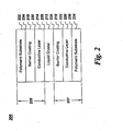
- FIG. 2 is a schematic representation of the structure of a flexible liquid crystal display of the present invention.
- Flexible LCD 200 comprises a center liquid crystal layer 212, a first and a second conductive layer 214, 216, a first and a second barrier layer 218, 220 and a first and a second polymeric substrate 222, 224.
- First polymeric substrate 222, first conductive layer 214 and first barrier layer 218 combine to form a first plate 225 and second polymeric substrate 224, second conductive layer 216 and second barrier layer 220 combine to form a second plate 227.
- First and second plates 225, 227 are disposed substantially parallel to one another and liquid crystal layer 212 is interposed therebetween.
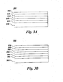
- Figures 3a and 3b are schematic representations of a light emitting diode (LED) and an organic electroluminescent device (OELD), respectively.
- LED 300 Figure 3a
- barrier layer 312 is disposed on substrate 310.
- Anode 314 is disposed on barrier layer 312 opposite substrate 310.
- Hole transport layer 315 which comprises at least one of the n-type (negative charge accepting) semiconductors known in the art, such as, but not limited to, silicon doped with phosphorous, is disposed on top of - and in contact with - anode 314.
- Electron transport layer 316 comprising at least one the p-type (positive hole) semiconductors known in the art, such as, but not limited to, silicon doped with aluminum, is disposed on top of and in contact with hole transport layer 315.
- Cathode 318 is disposed on top of - and in contact with - electron transport layer 316.
- OELD 350 ( Figure 3b) also includes a substrate 360, barrier layer 362, anode 364, hole transport layer 366, electron transport layer 370, and cathode 372 in substantially the same relation as in LED 300, with the exception that emission layer 368 is disposed between hole transport layer 366 and electron transport layer 370.
- Hole transport layer 366, emission layer 368, and electron transport layer 370 each comprise an organic material in either molecular or polymeric form. Electron transport layer 370 and emission layer 368 may be combined into a single layer. Alternatively, hole transport layer 366, emission layer 368, and electron transport layer 370 may be combined into a single layer.
- the at least one layer 110 may comprise at least one of an adhesion layer, an abrasion-resistant layer, an ultraviolet radiation-absorbing layer, and an infrared radiation-reflecting layer.
- the adhesion layer comprises at least one of a metal in elemental form, a metal carbide, a metal oxycarbide, a metal oxide, a metal nitride, a metal oxynitride, and a metal carbonitride, wherein the metal is one of silicon, aluminum, titanium, zirconium, hafnium, tantalum, gallium, germanium, zinc, tin, cadmium, tungsten, molybdenum, chromium, vanadium, and platinum.
- the adhesion layer may comprise at least one of: amorphous carbon; a ceramic comprising at least one of glass, silica, alumina, zirconia, boron nitride, boron carbide, and boron carbonitride; a silicone; monomers; oligomers; a siloxane; a polymer; an epoxide; an acrylate; an acrylonitrile; a xylene; a styrene; and the like, as well as combinations thereof.
- the ultraviolet radiation-absorbing layer comprises at least one of titanium oxide, zinc oxide, cerium oxide, an ultraviolet radiation-absorbing organic material in either polymeric or molecular form, and combinations thereof.
- the infrared radiation-reflecting layer when included in the at least one layer 110, comprises at least one of silver, aluminum, indium, tin, indium tin oxide, cadmium stannate, zinc, and combinations thereof.
- the at least one barrier layer 106 is interposed between the at least one layer 110 and substrate 102.
- the at least one layer 110 may be disposed between barrier layer 106 and a second barrier layer 105.
- the at least one layer 110 need only be disposed between a portion of barrier layer 106 and second barrier layer 105, as seen in Figure 1.
- Such a configuration provides all-around encapsulation and protection of the at least one layer 110 from exposure to water vapor and oxygen.
- the at least one layer 110 is interposed between the at least one barrier layer 106 and substrate 102 (as represented by 104 in Figure 1).
- One example of the latter embodiment is when the at least one layer 110 comprises an adhesion layer.
- the present invention also includes a method of forming the article 100 having barrier layer 106 disposed on substrate 102, as described herein, and a method of forming barrier layer 106, which is described herein, on substrate 102.
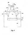
- Barrier layer 106 is formed on substrate 102 by injecting at least one reactant gas into a plasma, which is generated by at least one plasma source.
- the at least one plasma source is preferably an expanding thermal plasma (also referred to hereinafter as "ETP") source that produces an expanding thermal plasma.
- EDP expanding thermal plasma
- Either a single plasma source or an array of a plurality of plasma sources may be used to generate the plasma.
- Systems having single and multiple plasma sources have been described in: "Protective Coating by High Rate Arc Plasma Deposition," U.S.
- Patent 6,110,544, by Barry Lee-Mean Yang et al. "Apparatus and Method for Large Area Chemical Vapor Deposition Using Expanding Thermal Plasma Generators," U.S. Patent Application 09/681,820, by Barry Lee-Mean Yang et al.; “Large Area Plasma Coating Using Multiple Expanding Thermal Plasma Sources in Combination with a Common Injection Source,” U.S. Patent Application 09/683,149, by Marc Schaepkens; and “Apparatus and Method for Depositing Large Area Coatings on Non-Planar Surfaces," U.S. Patent Application 09/683,148, by Marc Schaepkens, all of which are incorporated herein by reference in their entirety.
- ETP deposition system 400 includes high pressure plasma chamber 410 and a low pressure deposition chamber 420, the latter containing substrate 424.
- ETP source 402 includes a cathode 404, an anode 406, and a plasma source gas inlet 408, of which the latter two are disposed in plasma chamber 410.
- the plasma source gas is an inert gas, such as a noble gas; i.e., argon, helium, neon, krypton, or xenon.
- chemically reactive gases such as, but not limited to, nitrogen and hydrogen, may be used as the plasma source gas.
- argon is used as the plasma source gas.
- a plasma 412 which is an expanding thermal plasma, is generated in ETP source 402 by striking an arc between cathode 404 and anode 406 while introducing the plasma source gas into the arc through plasma source gas inlet 408.
- Plasma chamber 410 and deposition chamber 420 are in fluid communication with each other through opening 418.
- Deposition chamber 420 is in fluid communication with a vacuum system (not shown), which is capable of maintaining the deposition chamber at a pressure that is lower than that of plasma chamber 410.
- the deposition chamber 420 is maintained at a pressure of less than about 1 torr (about 133 Pa) and, preferably, at a pressure of less than about 100 millitorr (about 0. 133 Pa), while plasma chamber 410 is maintained at a pressure of at least about 0.1 atmosphere (about 1.01 ⁇ 10 4 Pa).
- At least one reactant gas injector 422 is located in deposition chamber 420 for providing at least one reactant gas at a predetermined flow rate into the plasma generated by plasma source 402.
- the at least one reactant gas is provided through at least one reactant gas injector 422 to plasma 412 as the plasma 412 enters deposition chamber 420 through opening 418.
- the at least one reactant gas may comprise a single reactant gas or a mixture of reactant gases.
- the at least one reactant gas may be provided from a single reactant gas source or separate, multiple reactant gas sources to either a single reactant gas injector system or separate reactant gas injector systems.
- a plasma is generated by ionizing the plasma source gas in the arc generated between the cathode and anode to produce a positive ion and an electron.
- the following reaction for example, occurs when an argon plasma is generated: Are ⁇ Ar + + e - .
- the plasma is then expanded into a high volume at low pressure, thereby cooling the electrons and positive ions.
- plasma 412 is generated in plasma chamber 410 and expanded into deposition chamber 420 through opening 418.
- deposition chamber 420 is maintained at a significantly lower pressure than plasma chamber 410. Consequently, the electrons in the ETP are too cold and thus have insufficient energy to cause direct dissociation of the at least one reactant gas within the ETP. Instead, the at least one reactant gas that is introduced into the plasma may undergo charge exchange and dissociative recombination reactions with the ions and electrons within the ETP to form at least one deposition precursor.
- the positive ion and electron temperatures are approximately equal and in the range of about 0.1 eV (about 1000 K).
- other types of plasmas produce electrons having a sufficiently high temperature to substantially affect the chemistry of the plasma.
- the positive ions typically have a temperature of greater than 0.1 eV, and the electrons have a temperature of at least 1 eV, or about 10,000 K.
- the at least one reactant gas undergoes a reaction within the ETP to form at least one deposition precursor.
- Such reactions may include, but are not limited to, charge exchange reactions, dissociative recombination reactions, and fragmentation reactions.
- the at least one deposition precursor that is formed within the ETP is then deposited on a surface of substrate 424 to form the barrier layer 106 on substrate 424.
- the at least one deposition precursor is deposited on substrate 424 at a rate of at least about 200 nm/min to form the at least one barrier layer 106 on substrate 424, although higher deposition rates are within the scope of the invention.
- the at least one deposition precursor is deposited on substrate 424 at a rate of at least about 600 nm/min.
- the at least one deposition precursor is deposited on substrate 424 at a rate of at least about 3,000 nm/min.
- the at least one deposition precursor is deposited on a surface of substrate 424 at a rate of at least about 10,000 nm/min.
- the at least one barrier layer 106 comprises at least one of a metal oxide, a metal nitride, a metal carbide, and combinations thereof, wherein the metal is one of silicon, aluminum, zinc, indium, tin, and a transition metal, such as, but not limited to, titanium.
- the at least one reactant gas includes a first gaseous reagent comprising at least one of a silane, a metal vapor, a metal halide, and an organic compound of a metal, wherein the metal is one of titanium, zinc, aluminum, indium, and tin.
- Exemplary silanes include disilanes, aminosilanes, and chlorosilanes.
- Exemplary organic compounds include titanium isopropoxide, diethyl zinc, dimethyl zinc, indium isopropoxide, indium tert-butoxide, aluminum isopropoxide, and combinations thereof.
- Exemplary metal halides include the chlorides of titanium, tin, and aluminum.
- the at least one reactant may also comprise elemental zinc, indium, tin, and aluminum in vapor form.
- the first gaseous reagent is injected into plasma 412 along with a second gaseous reagent comprising at least one of oxygen, nitrogen, hydrogen, water, and ammonia.
- a first gaseous reagent comprising at least one of titanium chloride and titanium isopropoxide is injected into plasma 412 along with a second reagent, which, in addition to - or instead of - oxygen, nitrogen, hydrogen, water, and ammonia, may include propane, butane, acetylene, and the like, as well as combinations thereof.
- a first gaseous reagent comprising at least one of a silane, a disilane, an aminosilane, and a chlorosilane is injected into plasma 412 along with the second reagent.
- a silicon nitride barrier layer may be deposited by injecting silane (SiH 4 ), diluted in helium to a concentration of about 2% and ammonia into an expanding thermal argon plasma.
- article 100 may further include at least one layer 110 in addition to the at least one barrier layer 106.
- the method of forming the article 100 having barrier layer 106 disposed on substrate 102, and the method of forming barrier layer 106 on substrate 102, both of which are described herein, may further include at least one step in which the at least one layer 110 is applied to either substrate 102 or barrier layer 106.
- the method by which the at least one layer 110 is deposited will depend upon the nature and properties (e.g., composition, desired physical properties, and the like) of the at least one coating.
- the at least one layer 110 may be deposited using the ETP plasma apparatus and method described herein.
- the at least one layer 110 may be deposited using methods such as, for example, sputtering, evaporation, ion beam assisted deposition (IBAD), plasma enhanced chemical vapor deposition (PEVCD), high intensity plasma chemical vapor deposition (HIPCVD) using either an inductively coupled plasma (ICP) or electron cyclotron resonance (ECR), and the like.
- IBAD ion beam assisted deposition
- PEVCD plasma enhanced chemical vapor deposition
- HPCVD high intensity plasma chemical vapor deposition
- ICP inductively coupled plasma
- ECR electron cyclotron resonance
- a polycarbonate substrate having a thickness of 30 mil (about 0.76 mm) was placed in the deposition chamber of a plasma deposition system similar to that described in the present application and schematically shown in Figure 4.
- the substrate was positioned at a working distance (WD) ranging from about 25 cm to about 60 cm from the expanding thermal plasma (ETP) source.
- the vacuum vessel was evacuated to a pressure of less than about 100 mTorr (millitorr), argon gas was flowed through into the plasma chamber and the ETP source at a rate in a range from about 2 slm (standard liters per minute) to about 3 slm, and the plasma source was ignited.
- the ETP operated at a current level in the range form about 40 A to about 70 A.
- the pressure within the plasma chamber was in the range from about 300 torr to about 800 torr, whereas the pressure within the deposition chamber was in the range from about 45 mtorr to about 100 mtorr.
- the pressure differential caused the argon thermal plasma to expand into the deposition chamber, where reagents, comprising silane diluted in helium to a concentration of about 2% and ammonia, were injected through a ring injector into the expanding argon thermal plasma.
- the reagents reacted with the ETP to form deposition precursors, which then combined to deposit a silicon nitride material barrier layer on the polycarbonate substrate at a deposition rate of at least 200 nm/min.
- a plot of the water vapor transmission rate (WVTR) at 25°C and 100% relative humidity and 100% relative humidity of the silicon nitride barrier layer as a function of reagent (in this case, ammonia) flow rate is shown in Figure 5.
- the WVTR for an uncoated polycarbonate film having a thickness of 30 mil is also shown in Figure 5.
- a single 350 nm thick silicon nitride barrier layer deposited on a polycarbonate film having a thickness of about 30 mil reduces the WVTR to less than 0.2 g/m 2 -day.
- the films are highly transparent and colorless; the polycarbonate film with the silicon nitride barrier layer has a transparency of at least 89% and a yellow-index of less than 0.7.
- articles other than flexible LCD displays, LEDs and OELDs, that comprise a substrate and a barrier having the properties described herein are also considered to be within the scope of the present invention.
- Such articles include, but are not limited to, photovoltaic devices, electrochromic devices, x-ray imaging devices, organic integrated circuits, and rigid-substrate display devices. Accordingly, various modifications, adaptations, and alternatives may occur to one skilled in the art without departing from the scope of the present invention.
Abstract
Description
- The invention relates to a barrier layer that is resistant to the transmission of moisture and oxygen. More particularly, the present invention relates to an article having such a barrier layer and methods of applying such a barrier layer to an article.
- Different types of electronic devices such as, but not limited to, light emitting diodes (also referred hereinafter as "LEDs"), liquid crystal displays (also referred hereinafter as "LCDs"), photovoltaic articles, flat panel display devices, electrochromic articles, and organic electroluminescent devices (also referred hereinafter as "OELDs") share a common architecture: each device includes at least one substrate and at least one "active" layer.
- Many of the materials that are used in the active layers of such devices are sensitive to environmental factors. Electrode materials in LEDs and OELDs are sensitive to air and moisture, as are the polymeric and organic compounds that are used in OELDs and the liquid crystal materials in LCDs. Exposure to the elements-particularly oxygen and water - may severely limit the lifetime of such devices.
- Selection of a substantially impermeable substrate, such as glass, provides protection from environmental attack. Polymeric substrates that are used in flexible versions of such devices, however, do not provide adequate protection against oxygen and moisture. Consequently, at least one coating that is substantially impermeable to oxygen and water vapor must be applied to the polymeric substrate to achieve the desired level of protection.
- Barrier materials have been applied to substrates using a variety of coating processes. Plasma enhanced chemical vapor deposition (PECVD), for example, has been used to deposit barrier materials. Typical PECVD processes, however, are relatively slow; i.e. the barrier material is deposited on the substrate at a rate of about 30 to 60 nm/min or less. In order to be commercially viable, the barrier coating must be applied to the substrate at a significantly higher deposition rate.
- While barrier materials are needed to extend lifetimes of flexible display devices such as LCDs, LEDs, and OELDs to acceptable levels, the methods that are currently used to apply the needed barrier materials to substrates are too slow. Therefore, what is needed is a method of forming a barrier layer on a substrate at a high rate of deposition. What is also needed is a method of forming a barrier layer on a substrate to form an article having acceptable water vapor and oxygen transmission rates. What is further needed is an article having a barrier layer, the article having acceptable water vapor and oxygen transmission rates.
- The present invention meets these and other needs by providing an article comprising a substrate having a barrier layer disposed on the surface of the substrate and methods of depositing such a barrier layer on the substrate, wherein the barrier layer is resistant to transmission of moisture and oxygen therethrough. The article may include additional layers, such as, but not limited to, an adhesion layer, abrasion resistant layers, radiation-absorbing layers, radiation-reflective layers, and conductive layers. Such articles include, but are not limited to, light emitting diodes (LEDs), liquid crystal displays (LCDs), photovoltaic articles, electrochromic articles, organic integrated circuits, and organic electroluminescent devices (OELDs).
- Accordingly, one aspect of the invention is to provide an article. The article comprises a substrate and at least one barrier layer disposed on at least one surface of the substrate, wherein the barrier layer comprises an inorganic material, and wherein the barrier layer is resistant to transmission of moisture and oxygen therethrough and has a water vapor transmission rate (WVTR) at 25°C and 100% relative humidity of less than about 2 g/m2-day and an oxygen transmission rate (OTR) at 25°C and 100% oxygen concentration of less than about 2 cc/m2-day.
- A second aspect of the invention is to provide a barrier layer that is resistant to transmission of moisture and oxygen therethrough. The barrier layer comprises at least one of a metal oxide, a metal nitride, a metal carbide, and combinations thereof. Each of the metal nitride, the metal carbide, and the metal oxide contains at least one of silicon, aluminum, zinc, indium, tin, a transition metal, and combinations thereof. The barrier layer has a water vapor transmission rate (WVTR) at 25°C and 100% relative humidity of less than about 2 g/m2-day and an oxygen transmission rate (OTR) at 25°C and 100% oxygen concentration of less than about 2 cc/m2-day.
- A third aspect of the invention is to provide an article. The article comprises a substrate and at least one barrier layer, the at least one barrier layer comprising at least one of a metal oxide, a metal nitride, a metal carbide, and combinations thereof, wherein each of the metal nitride, the metal carbide, and the metal oxide contains at least one of silicon, aluminum, zinc, indium, tin, a transition metal, and combinations thereof, and wherein the barrier layer is resistant to transmission of moisture and oxygen therethrough and has a water vapor transmission rate (WVTR) at 25°C and 100% relative humidity of less than about 2 g/m2-day and an oxygen transmission rate (OTR) at 25°C and 100% oxygen concentration of less than about 2 cc/m2-day.
- A fourth aspect of the invention is to provide a method of forming a coated article. The coated article comprises a substrate and a barrier layer disposed thereon, wherein the barrier layer is resistant to transmission of moisture and oxygen therethrough and has a water vapor transmission rate (WVTR) at 25°C and 100% relative humidity of less than about 2 g/m2-day and an oxygen transmission rate (OTR) at 25°C and 100% oxygen concentration of less than about 2 cc/m2-day. The method comprises the steps of: providing a substrate; generating a thermal plasma, the thermal plasma having an electron temperature of less than about 1eV; injecting at least one reagent into the thermal plasma; reacting the at least one reagent in the thermal plasma to form at least one deposition precursor; and depositing the at least one deposition precursor on the substrate at a rate of at least about 200 nm/min to form the barrier layer on the substrate.
- A fifth aspect of the invention is to provide a method of forming a barrier layer on a substrate. The barrier layer is resistant to transmission of moisture and oxygen therethrough and has a water vapor transmission rate (WVTR) at 25°C and 100% relative humidity of less than about 2 g/m2-day and an oxygen transmission rate (OTR) at 25°C and 100% oxygen concentration of less than about 2 cc/m2-day, and comprises at least one of at least one of a metal oxide, a metal nitride, a metal carbide, and combinations thereof, wherein each of the metal nitride, the metal carbide, and the metal oxide contains at least one of silicon, aluminum, zinc, indium, tin, a transition metal, and combinations thereof. The method comprises the steps of: generating a thermal plasma, the thermal plasma having an electron temperature of less than about 1eV; injecting a first reagent into the thermal plasma, the first reagent comprising at least one of silicon, aluminum, zinc, indium, tin, a transition metal, and combinations thereof; injecting a second reagent into the thermal plasma, the second reagent comprising at least one of oxygen, nitrogen, and ammonia; decomposing the first reagent and the second reagent in the thermal plasma to form a plurality of decomposition products; reacting the at least one reagent in the thermal plasma to form at least one deposition precursor; and depositing the at least one deposition precursor on the substrate at a rate of at least about 200 nm/min to form the barrier layer comprising at least one of a metal oxide, a metal nitride, a metal carbide, and combinations thereof on the substrate.
- A sixth aspect of the invention is to provide a method of forming a coated article. The coated article comprises a substrate and a barrier layer disposed thereon. The barrier layer is resistant to transmission of moisture and oxygen therethrough and has a water vapor transmission rate (WVTR) at 25°C and 100% relative humidity of less than about 2 g/m2-day and an oxygen transmission rate (OTR) at 25°C and 100% oxygen concentration of less than about 2 cc/m2-day, and comprises at least one of a metal oxide, a metal nitride, a metal carbide, and combinations thereof, wherein each of the metal nitride, the metal carbide, and the metal oxide contains at least one of silicon, aluminum, zinc, indium, tin, a transition metal, and combinations thereof. The method comprises the steps of: providing a substrate; generating a thermal plasma, the thermal plasma having an electron temperature of less than about 1eV; injecting a first reagent into the thermal plasma, the first reagent comprising at least one of silicon, aluminum, zinc, indium, tin, a transition metal, and combinations thereof; injecting a second reagent into the thermal plasma, the second reagent comprising at least one of oxygen, nitrogen, and ammonia; reacting the first reagent and the second reagent in the thermal plasma to form at least one deposition precursor; and depositing the at least one deposition precursor on the substrate at a rate of at least about 200 nm/min, thereby forming the barrier layer comprising at least one of a metal oxide, a metal nitride, a metal carbide, and combinations thereof on the substrate.
- These and other aspects, advantages, and salient features of the present invention will become apparent from the following detailed description, by way of example, with reference to the accompanying drawings, in which.
- FIGURE 1 is a schematic representation of an article of the present invention;
- FIGURE 2 is a schematic representation of a flexible liquid crystal display of the present invention;
- FIGURE 3a is a schematic representation of a light emitting diode of the present invention;
- FIGURE 3b is a schematic representation of a organic electroluminescent device of the present invention;
- FIGURE 4 is a schematic representation of an expanding thermal plasma deposition system; and
- FIGURE 5 is a plot of the water vapor transmission rate of a silicon nitride barrier layer of the present invention as a function of reagent flow rate.
-
- In the following description, like reference characters designate like or corresponding parts throughout the several views shown in the figures. It is also understood that terms such as "top," "bottom," "outward," "inward," and the like are words of convenience and are not to be construed as limiting terms.
- Several display devices such as, but not limited to, light emitting diodes (also referred hereinafter as "LEDs"), liquid crystal displays (also referred hereinafter as "LCDs"), photovoltaic articles, flat panel display devices, electrochromic articles, and organic electroluminescent devices (also referred hereinafter as "OELDs") share a common architecture: each device includes at least one substrate and at least one "active" layer. Light emitting diodes and organic electroluminescent devices, for example, may include a cathode layer, an electron transport layer, an emission layer, a hole transport layer, and an anode layer disposed on a substrate. Liquid crystal displays may include two substrates, each having an electrically conductive layer disposed thereon, and a liquid crystal layer sandwiched between the two substrates.
- Many of the materials that are used in these devices may be adversely affected by environmental factors. Electrode materials in LEDs and OELDs are sensitive to air and moisture, as are the polymeric and organic compounds that are used in OELDs and the liquid crystal materials in LCDs. Exposure to the elements-particularly oxygen and water - may severely limit the lifetime of such devices.
- Selection of a substantially impermeable substrate, such as glass, provides protection from environmental attack. Polymeric substrates that are used in flexible versions of such devices, however, do not provide adequate protection against oxygen and moisture. Consequently, at least one barrier layer that is substantially impermeable to oxygen and water vapor must be applied to the polymeric substrate to achieve the desired level of protection. Here, a coating, device, or coated substrate that is described as being "substantially impermeable" is understood as having a water vapor transmission rate (also referred hereinafter as "WVTR") and an oxygen transmission rate (also referred hereinafter as "OTR") of less than about 2 g/m2-day at 25°C and 100% relative humidity and less than about 2 cc/m2-day at 25°C and 100% oxygen concentration, respectively.
- Referring to the drawings in general and to Figure 1 in particular, it will be understood that the illustrations are for the purpose of describing a preferred embodiment of the invention and are not intended to limit the invention thereto. Figure 1 is a schematic representation of an
article 100 of the present invention.Article 100 comprises asubstrate 102 and at least onebarrier layer 106 disposed on a surface ofsubstrate 102. Anadditional layer 104, such as, but not limited to, an adhesion layer, may be optionally disposed betweensubstrate 102 and the at least onebarrier layer 106.Substrate 102 may comprise one of glass, a polymeric material, silicon, a metallic web, and fiberglass. Wheresubstrate 102 is a polymeric material,substrate 102 comprises at least one of a polycarbonate, a polyethylene terephtalene, a polyethylene naphthalene, a polyimide, a polyethersulfone, a polyacrylate, a polynorbomene, and combinations thereof. In another embodiment,substrate 102 is a metallic web comprising one of aluminum and steel. - The at least one
barrier layer 106 comprises an inorganic material and is resistant to the transmission of moisture and oxygen therethrough. The at least onebarrier layer 106 has a WVTR of less than about 2 g/m2-day at 25°C and 100% relative humidity and an OTR of less than about 2 cc/m2-day at 25°C and 100% oxygen concentration. In a second embodiment, the at least onemoisture layer 106 has a WVTR of less than about 1.7 g/m2-day at 25°C and 100% relative humidity and an OTR of less than about 0.21 cc/m2-day at 25°C and 100% oxygen concentration. In a third embodiment, the at least onebarrier layer 106 has a WVTR of less than about 0.157 g/m2-day at 25°C and 100% relative humidity and an OTR of less than about 0.13 cc/m2-day at 25°C and 100% oxygen concentration. The at least onebarrier layer 106 comprises at least one of a metal oxide, a metal nitride, a metal carbide, and combinations thereof, wherein the metal is one of silicon, aluminum, zinc, indium, tin, and a transition metal, such as, but not limited to, titanium. In one embodiment, the at least onebarrier layer 106 comprises titanium oxide. In another embodiment, the at least onebarrier layer 106 comprises silicon nitride. The at least onebarrier layer 106 has a thickness in a range from about 10 nm to about 10,000 nm. In one embodiment, the at least one barrier layer has a thickness in a range from about 20 nm to about 500 nm. -
Article 100 may further include at least onelayer 110, which is disposed adjacent to the at least onebarrier layer 106. Wherearticle 100 is a LCD display, the at least one layer may include at least one transparent electrically conductive layer comprising an oxide of tin, cadmium, indium, zinc, magnesium, gallium, and combinations thereof. Wherearticle 100 is an LED or OELD, the at least one layer may include, for example, a cathode layer, an electron transport layer, an emission layer (in OELDs), a hole transport layer, and an anode layer, wherein the electron transport and hole transport layers may be either organic or inorganic material, and wherein the emission layer comprises an organic material. - Figure 2 is a schematic representation of the structure of a flexible liquid crystal display of the present invention.
Flexible LCD 200 comprises a centerliquid crystal layer 212, a first and a secondconductive layer second barrier layer polymeric substrate polymeric substrate 222, firstconductive layer 214 andfirst barrier layer 218 combine to form afirst plate 225 and secondpolymeric substrate 224, secondconductive layer 216 andsecond barrier layer 220 combine to form asecond plate 227. First andsecond plates liquid crystal layer 212 is interposed therebetween. Flexible LCDs have been described in "A Transparent Flexible Barrier for Liquid Crystal Display Devices and Method of Making the Same," U.S. Patent Application 09/836,657, by Argemiro Soares DaSilva Sobrinho, which is incorporated herein by reference in its entirety. - Figures 3a and 3b are schematic representations of a light emitting diode (LED) and an organic electroluminescent device (OELD), respectively. In LED 300 (Figure 3a),
barrier layer 312 is disposed onsubstrate 310.Anode 314 is disposed onbarrier layer 312opposite substrate 310.Hole transport layer 315, which comprises at least one of the n-type (negative charge accepting) semiconductors known in the art, such as, but not limited to, silicon doped with phosphorous, is disposed on top of - and in contact with -anode 314.Electron transport layer 316, comprising at least one the p-type (positive hole) semiconductors known in the art, such as, but not limited to, silicon doped with aluminum, is disposed on top of and in contact withhole transport layer 315.Cathode 318 is disposed on top of - and in contact with -electron transport layer 316. - OELD 350 (Figure 3b) also includes a
substrate 360,barrier layer 362,anode 364,hole transport layer 366,electron transport layer 370, andcathode 372 in substantially the same relation as inLED 300, with the exception thatemission layer 368 is disposed betweenhole transport layer 366 andelectron transport layer 370.Hole transport layer 366,emission layer 368, andelectron transport layer 370 each comprise an organic material in either molecular or polymeric form.Electron transport layer 370 andemission layer 368 may be combined into a single layer. Alternatively,hole transport layer 366,emission layer 368, andelectron transport layer 370 may be combined into a single layer. - In other embodiments, the at least one
layer 110 may comprise at least one of an adhesion layer, an abrasion-resistant layer, an ultraviolet radiation-absorbing layer, and an infrared radiation-reflecting layer. When the at least onelayer 110 comprises an adhesion layer, which is intended to promote adhesion ofbarrier layer 106 tosubstrate 102, the adhesion layer comprises at least one of a metal in elemental form, a metal carbide, a metal oxycarbide, a metal oxide, a metal nitride, a metal oxynitride, and a metal carbonitride, wherein the metal is one of silicon, aluminum, titanium, zirconium, hafnium, tantalum, gallium, germanium, zinc, tin, cadmium, tungsten, molybdenum, chromium, vanadium, and platinum. Alternatively, the adhesion layer may comprise at least one of: amorphous carbon; a ceramic comprising at least one of glass, silica, alumina, zirconia, boron nitride, boron carbide, and boron carbonitride; a silicone; monomers; oligomers; a siloxane; a polymer; an epoxide; an acrylate; an acrylonitrile; a xylene; a styrene; and the like, as well as combinations thereof. When included in the at least onelayer 110, the ultraviolet radiation-absorbing layer comprises at least one of titanium oxide, zinc oxide, cerium oxide, an ultraviolet radiation-absorbing organic material in either polymeric or molecular form, and combinations thereof. The infrared radiation-reflecting layer, when included in the at least onelayer 110, comprises at least one of silver, aluminum, indium, tin, indium tin oxide, cadmium stannate, zinc, and combinations thereof. - In one embodiment, the at least one
barrier layer 106 is interposed between the at least onelayer 110 andsubstrate 102. In one embodiment, shown in Figure 1, the at least onelayer 110 may be disposed betweenbarrier layer 106 and asecond barrier layer 105. In addition, the at least onelayer 110 need only be disposed between a portion ofbarrier layer 106 andsecond barrier layer 105, as seen in Figure 1. Such a configuration provides all-around encapsulation and protection of the at least onelayer 110 from exposure to water vapor and oxygen. In another embodiment, the at least onelayer 110 is interposed between the at least onebarrier layer 106 and substrate 102 (as represented by 104 in Figure 1). One example of the latter embodiment is when the at least onelayer 110 comprises an adhesion layer. - The present invention also includes a method of forming the
article 100 havingbarrier layer 106 disposed onsubstrate 102, as described herein, and a method of formingbarrier layer 106, which is described herein, onsubstrate 102.Barrier layer 106 is formed onsubstrate 102 by injecting at least one reactant gas into a plasma, which is generated by at least one plasma source. The at least one plasma source is preferably an expanding thermal plasma (also referred to hereinafter as "ETP") source that produces an expanding thermal plasma. Either a single plasma source or an array of a plurality of plasma sources may be used to generate the plasma. Systems having single and multiple plasma sources have been described in: "Protective Coating by High Rate Arc Plasma Deposition," U.S. Patent 6,110,544, by Barry Lee-Mean Yang et al.; "Apparatus and Method for Large Area Chemical Vapor Deposition Using Expanding Thermal Plasma Generators," U.S. Patent Application 09/681,820, by Barry Lee-Mean Yang et al.; "Large Area Plasma Coating Using Multiple Expanding Thermal Plasma Sources in Combination with a Common Injection Source," U.S. Patent Application 09/683,149, by Marc Schaepkens; and "Apparatus and Method for Depositing Large Area Coatings on Non-Planar Surfaces," U.S. Patent Application 09/683,148, by Marc Schaepkens, all of which are incorporated herein by reference in their entirety. - A schematic representation of an ETP deposition system having a single ETP source is shown in Figure 4.
ETP deposition system 400 includes highpressure plasma chamber 410 and a lowpressure deposition chamber 420, thelatter containing substrate 424.ETP source 402 includes acathode 404, ananode 406, and a plasmasource gas inlet 408, of which the latter two are disposed inplasma chamber 410. The plasma source gas is an inert gas, such as a noble gas; i.e., argon, helium, neon, krypton, or xenon. Alternatively, chemically reactive gases, such as, but not limited to, nitrogen and hydrogen, may be used as the plasma source gas. Preferably, argon is used as the plasma source gas. Aplasma 412, which is an expanding thermal plasma, is generated inETP source 402 by striking an arc betweencathode 404 andanode 406 while introducing the plasma source gas into the arc through plasmasource gas inlet 408. -
Plasma chamber 410 anddeposition chamber 420 are in fluid communication with each other throughopening 418.Deposition chamber 420 is in fluid communication with a vacuum system (not shown), which is capable of maintaining the deposition chamber at a pressure that is lower than that ofplasma chamber 410. In one embodiment, thedeposition chamber 420 is maintained at a pressure of less than about 1 torr (about 133 Pa) and, preferably, at a pressure of less than about 100 millitorr (about 0. 133 Pa), whileplasma chamber 410 is maintained at a pressure of at least about 0.1 atmosphere (about 1.01×10⁴Pa). - At least one
reactant gas injector 422 is located indeposition chamber 420 for providing at least one reactant gas at a predetermined flow rate into the plasma generated byplasma source 402. The at least one reactant gas is provided through at least onereactant gas injector 422 toplasma 412 as theplasma 412 entersdeposition chamber 420 throughopening 418. The at least one reactant gas may comprise a single reactant gas or a mixture of reactant gases. The at least one reactant gas may be provided from a single reactant gas source or separate, multiple reactant gas sources to either a single reactant gas injector system or separate reactant gas injector systems. - In an ETP, a plasma is generated by ionizing the plasma source gas in the arc generated between the cathode and anode to produce a positive ion and an electron. The following reaction, for example, occurs when an argon plasma is generated:
- The plasma is then expanded into a high volume at low pressure, thereby cooling the electrons and positive ions. In the present invention,
plasma 412 is generated inplasma chamber 410 and expanded intodeposition chamber 420 throughopening 418. As previously described,deposition chamber 420 is maintained at a significantly lower pressure thanplasma chamber 410. Consequently, the electrons in the ETP are too cold and thus have insufficient energy to cause direct dissociation of the at least one reactant gas within the ETP. Instead, the at least one reactant gas that is introduced into the plasma may undergo charge exchange and dissociative recombination reactions with the ions and electrons within the ETP to form at least one deposition precursor. In the expanded ETP, the positive ion and electron temperatures are approximately equal and in the range of about 0.1 eV (about 1000 K). In contrast to an ETP, other types of plasmas produce electrons having a sufficiently high temperature to substantially affect the chemistry of the plasma. In such plasmas, the positive ions typically have a temperature of greater than 0.1 eV, and the electrons have a temperature of at least 1 eV, or about 10,000 K. - Once injected into
plasma 412, the at least one reactant gas undergoes a reaction within the ETP to form at least one deposition precursor. Such reactions may include, but are not limited to, charge exchange reactions, dissociative recombination reactions, and fragmentation reactions. The at least one deposition precursor that is formed within the ETP is then deposited on a surface ofsubstrate 424 to form thebarrier layer 106 onsubstrate 424. - The at least one deposition precursor is deposited on
substrate 424 at a rate of at least about 200 nm/min to form the at least onebarrier layer 106 onsubstrate 424, although higher deposition rates are within the scope of the invention. In one embodiment, for example, the at least one deposition precursor is deposited onsubstrate 424 at a rate of at least about 600 nm/min. In yet another embodiment, the at least one deposition precursor is deposited onsubstrate 424 at a rate of at least about 3,000 nm/min. in still yet another embodiment, the at least one deposition precursor is deposited on a surface ofsubstrate 424 at a rate of at least about 10,000 nm/min. - As previously described, the at least one
barrier layer 106 comprises at least one of a metal oxide, a metal nitride, a metal carbide, and combinations thereof, wherein the metal is one of silicon, aluminum, zinc, indium, tin, and a transition metal, such as, but not limited to, titanium. In these instances, the at least one reactant gas includes a first gaseous reagent comprising at least one of a silane, a metal vapor, a metal halide, and an organic compound of a metal, wherein the metal is one of titanium, zinc, aluminum, indium, and tin. Exemplary silanes include disilanes, aminosilanes, and chlorosilanes. Exemplary organic compounds include titanium isopropoxide, diethyl zinc, dimethyl zinc, indium isopropoxide, indium tert-butoxide, aluminum isopropoxide, and combinations thereof. Exemplary metal halides include the chlorides of titanium, tin, and aluminum. The at least one reactant may also comprise elemental zinc, indium, tin, and aluminum in vapor form. The first gaseous reagent is injected intoplasma 412 along with a second gaseous reagent comprising at least one of oxygen, nitrogen, hydrogen, water, and ammonia. In one particular embodiment, where the at least onebarrier layer 106 comprises at least one of an oxide, a nitride, and a carbide of titanium, a first gaseous reagent comprising at least one of titanium chloride and titanium isopropoxide is injected intoplasma 412 along with a second reagent, which, in addition to - or instead of - oxygen, nitrogen, hydrogen, water, and ammonia, may include propane, butane, acetylene, and the like, as well as combinations thereof. In another embodiment in which the at least onebarrier layer 106 comprises at least one of an oxide, a nitride, and a carbide of silicon, a first gaseous reagent comprising at least one of a silane, a disilane, an aminosilane, and a chlorosilane is injected intoplasma 412 along with the second reagent. For example, a silicon nitride barrier layer may be deposited by injecting silane (SiH4), diluted in helium to a concentration of about 2% and ammonia into an expanding thermal argon plasma. - As previously described,
article 100 may further include at least onelayer 110 in addition to the at least onebarrier layer 106. In such instances, the method of forming thearticle 100 havingbarrier layer 106 disposed onsubstrate 102, and the method of formingbarrier layer 106 onsubstrate 102, both of which are described herein, may further include at least one step in which the at least onelayer 110 is applied to eithersubstrate 102 orbarrier layer 106. It will be appreciated by those skilled in the art that the method by which the at least onelayer 110 is deposited will depend upon the nature and properties (e.g., composition, desired physical properties, and the like) of the at least one coating. The at least onelayer 110 may be deposited using the ETP plasma apparatus and method described herein. Alternatively, the at least onelayer 110 may be deposited using methods such as, for example, sputtering, evaporation, ion beam assisted deposition (IBAD), plasma enhanced chemical vapor deposition (PEVCD), high intensity plasma chemical vapor deposition (HIPCVD) using either an inductively coupled plasma (ICP) or electron cyclotron resonance (ECR), and the like. - The following example serves to illustrate the salient features and advantages of the present invention.
- A polycarbonate substrate having a thickness of 30 mil (about 0.76 mm) was placed in the deposition chamber of a plasma deposition system similar to that described in the present application and schematically shown in Figure 4. The substrate was positioned at a working distance (WD) ranging from about 25 cm to about 60 cm from the expanding thermal plasma (ETP) source. The vacuum vessel was evacuated to a pressure of less than about 100 mTorr (millitorr), argon gas was flowed through into the plasma chamber and the ETP source at a rate in a range from about 2 slm (standard liters per minute) to about 3 slm, and the plasma source was ignited. The ETP operated at a current level in the range form about 40 A to about 70 A. The pressure within the plasma chamber was in the range from about 300 torr to about 800 torr, whereas the pressure within the deposition chamber was in the range from about 45 mtorr to about 100 mtorr. The pressure differential caused the argon thermal plasma to expand into the deposition chamber, where reagents, comprising silane diluted in helium to a concentration of about 2% and ammonia, were injected through a ring injector into the expanding argon thermal plasma. The reagents reacted with the ETP to form deposition precursors, which then combined to deposit a silicon nitride material barrier layer on the polycarbonate substrate at a deposition rate of at least 200 nm/min.
- A plot of the water vapor transmission rate (WVTR) at 25°C and 100% relative humidity and 100% relative humidity of the silicon nitride barrier layer as a function of reagent (in this case, ammonia) flow rate is shown in Figure 5. The WVTR for an uncoated polycarbonate film having a thickness of 30 mil is also shown in Figure 5. As seen in Figure 5, a single 350 nm thick silicon nitride barrier layer deposited on a polycarbonate film having a thickness of about 30 mil reduces the WVTR to less than 0.2 g/m2-day. The films are highly transparent and colorless; the polycarbonate film with the silicon nitride barrier layer has a transparency of at least 89% and a yellow-index of less than 0.7.
- While typical embodiments have been set forth for the purpose of illustration, the foregoing description should not be deemed to be a limitation on the scope of the invention. For example, articles, other than flexible LCD displays, LEDs and OELDs, that comprise a substrate and a barrier having the properties described herein are also considered to be within the scope of the present invention. Such articles include, but are not limited to, photovoltaic devices, electrochromic devices, x-ray imaging devices, organic integrated circuits, and rigid-substrate display devices. Accordingly, various modifications, adaptations, and alternatives may occur to one skilled in the art without departing from the scope of the present invention.
- For completeness, various aspects of the invention are set out in the following numbered clauses:
- 1. An article, said article comprising:
- a) a substrate; and
- b) at least one barrier layer disposed on at least one surface of said substrate, wherein said barrier layer comprises an inorganic material, and wherein said barrier layer is resistant to transmission of moisture and oxygen therethrough and has a water vapor transmission rate (WVTR) at 25°C and 100% relative humidity of less than about 2 g/m2-day and an oxygen transmission rate (OTR) at 25°C and 100% oxygen concentration of less than about 2 cc/m2-day.
- 2. The article according to Clause 1, further including at least one layer, wherein said at least one layer is disposed adjacent to said barrier layer.
- 3. The article according to
Clause 2, wherein said at least one barrier layer is interposed between said at least one layer and said substrate. - 4. The article according to
Clause 2, wherein said at least one layer is interposed between said at least one barrier layer and said substrate. - 5. The article according to Clause 4, wherein said at least one layer comprises an adhesion layer for promoting adhesion of said at least one barrier layer to said substrate.
- 6. The article according to Clause 5, wherein said adhesion layer comprises at least one of: a metal in elemental form, a carbide of said metal, an oxycarbide of said metal, an oxide of said metal, and a nitride of said metal, wherein said metal is one of silicon, aluminum, titanium, zirconium, hafnium, tantalum, gallium, germanium, zinc, tin, cadmium, tungsten, molybdenum, chromium, vanadium, and platinum; amorphous carbon; a ceramic material, wherein said ceramic material comprises at least one of glass, silica, alumina, zirconia, boron nitride, boron carbide, and boron carbonitride; a silicone; a siloxane; a polymer; an epoxide; an acrylate; an acrylonitrile; a xylene; a styrene; and combinations thereof.
- 7. The article according to
Clause 2, wherein said at least one layer comprises at least one of an abrasion resistant layer, an ultraviolet radiation-absorbing layer, an infrared radiation-reflecting layer, and an electrically conducting layer. - 8. The article according to Clause 7, wherein said abrasion resistant layer comprises at least one of: a carbide of a metal, an oxycarbide of said metal, an oxide of said metal, and a nitride of said metal, wherein said metal is one of silicon, aluminum, titanium, zirconium, hafnium, tantalum, gallium, germanium, zinc, tin, cadmium, tungsten, molybdenum, chromium, vanadium, and platinum; amorphous carbon; a ceramic material, wherein said ceramic material comprises at least one of glass, silica, alumina, zirconia, boron nitride, boron carbide, and boron carbonitride; a silicone; a siloxane; polymerized monomers; polymerized oligomers; an organic polymer; an inorganic-organic polymer; an epoxide; an acrylate; an acrylonitrile; a xylene; a styrene; and combinations thereof.
- 9. The article according to Clause 7, wherein said ultraviolet radiation-absorbing layer comprises at least one of titanium oxide, zinc oxide, cerium oxide, a polymer, and combinations thereof.
- 10. The article according to Clause 7, wherein said infrared radiation-reflecting layer comprises at least one of silver, aluminum, indium, tin, indium tin oxide, cadmium stannate, zinc, and combinations thereof.
- 11. The article according to Clause 7, wherein said electrically conducting layer comprises at least one of silver, aluminum, indium, tin, indium tin oxide, cadmium stannate, zinc, and combinations thereof.
- 12. The article according to Clause 1, wherein said inorganic material comprises at least one of an oxide, a nitride, and a carbide of a metal, and combinations thereof.
- 13. The article according to Clause 12, wherein said metal is one of silicon, aluminum, zinc, indium, tin, a transition metal, and combinations thereof.
- 14. The article according to Clause 13, wherein said transition metal is titanium.
- 15. The article according to Clause 13, wherein said inorganic material comprises titanium oxide.
- 16. The article according to Clause 13, wherein said inorganic material comprises silicon nitride.
- 17. The article according to Clause 1, wherein said barrier layer has a thickness in a range from about 10 nm to about 10,000 nm.
- 18. The article according to Clause 17, wherein said barrier layer has a thickness in a range from about 20 nm to about 500 nm.
- 19. The article according to Clause 1, wherein said barrier layer has a water vapor transmission rate of up to about 0.2 g/m2-day.
- 20. The article according to Clause 1, wherein said barrier layer has an oxygen transmission rate at 25°C and 100% oxygen concentration of up to about 0.2 cc/m2-day.
- 21. The article according to Clause 1, wherein the article is one of a light emitting diode (LED), a liquid crystal display (LCD), a photovoltaic article, a flat panel display device, an electrochromic article, an organic integrated circuit, and an organic electroluminescent device (OELD).
- 22. The article according to Clause 1, wherein said barrier layer is deposited on said substrate by: injecting at least one reagent into an expanding thermal plasma; reacting said at least one reagent in said expanding thermal plasma to form at least one deposition precursor; and depositing said at least one deposition precursor on said substrate at a rate of at least about 200 nm/min to form said barrier layer on said substrate.
- 23. The article according to Clause 1, wherein said substrate comprises one of glass, a polymeric material, silicon, a metallic web, and fiberglass.
- 24. The article according to Clause 23, wherein said polymeric material comprises one of a polycarbonate, a polyethylene terephtalene, a polyethylene naphthalene, a polyimide, a polyethersulfone, a polyacrylate, a polynorbornene, and combinations thereof.
- 25. The article according to Clause 23, wherein said metallic web comprises one of aluminum and steel.
- 26. A barrier layer deposited on a substrate, said barrier layer comprising at least one of a metal oxide, a metal nitride, a metal carbide, and combinations thereof, and wherein each of said metal nitride, said metal carbide, and said metal oxide contains at least one of silicon, aluminum, zinc, indium, tin, a transition metal, and combinations thereof, and wherein said barrier layer is resistant to transmission of moisture and oxygen therethrough and has a water vapor transmission rate (WVTR) at 25°C and 100% relative humidity of less than about 2 g/m2-day and an oxygen transmission rate (OTR) at 25°C and 100% oxygen concentration of less than about 2 cc/m2-day.
- 27. The barrier layer according to Clause 26, wherein said transition metal is titanium.
- 28. The barrier layer according to Clause 26, wherein said barrier layer comprises titanium oxide.
- 29. The barrier layer according to Clause 26, wherein said barrier layer comprises silicon nitride.
- 30. The barrier layer according to Clause 26, wherein said barrier layer has a thickness in a range from about 10 nm to about 10,000 nm.
- 31. The barrier layer according to
Clause 30, wherein said barrier layer has a thickness in a range from about 20 nm to about 500 nm. - 32. The barrier layer according to Clause 26, wherein said barrier layer has a water vapor transmission rate of up to about 0.2 g/m2-day.
- 33. The barrier layer according to Clause 26, wherein said barrier layer has an oxygen transmission rate at 25°C and 100% oxygen concentration of up to about 0.2 cc/m2-day.
- 34. The barrier layer according to Clause 26, wherein said barrier layer is deposited on said substrate by: injecting a first reagent into an expanding thermal plasma, said first reagent comprising at least one of silicon, aluminum, zinc, indium, tin, a transition metal, and combinations thereof; injecting a second reagent into said expanding thermal plasma, the second reagent comprising at least one of oxygen, nitrogen, hydrogen, water, and ammonia; reacting said first reagent and said second reagent in said expanding thermal plasma to form at least one deposition precursor; and depositing said at least one deposition precursor on said substrate at a rate of at least about 200 nm/min to form said barrier layer on said substrate.
- 35. The barrier layer according to Clause 34, wherein the at least one deposition precursor is deposited at a rate of at least about 600 nm/min to form the barrier layer on said substrate.
- 36. The barrier layer according to Clause 34, wherein the at least one deposition precursor is deposited on said substrate at a rate of at least about 3,000 nm/min to form the barrier layer on said substrate.
- 37. An article, said article comprising:
- a) a substrate; and
- b) at least one barrier layer, said at least one barrier layer comprising at least one of a metal oxide, a metal nitride, a metal carbide, and combinations thereof, wherein each of said metal nitride, said metal carbide, and said metal oxide contains at least one of silicon, aluminum, zinc, indium, tin, a transition metal, and combinations thereof, and wherein said barrier layer is resistant to transmission of moisture and oxygen therethrough and has a water vapor transmission rate (WVTR) at 25°C and 100% relative humidity of less than about 2 g/m2-day and an oxygen transmission rate (OTR) at 25°C and 100% oxygen concentration of less than about 2 cc/m2-day.
- 38. The article according to
Clause 37, further including at least one layer, wherein said at least one layer is disposed adjacent to said barrier layer. - 39. The article according to
Clause 38, wherein said at least one barrier layer is interposed between said at least one layer and said substrate. - 40. The article according to
Clause 38, wherein said at least one layer is interposed between said at least one barrier layer and said substrate. - 41. The article according to
Clause 40, wherein said at least one layer comprises an adhesion layer for promoting adhesion of said at least one barrier layer to said substrate. - 42. The article according to Clause 41, wherein said adhesion layer comprises at least one of: a metal in elemental form, a carbide of said metal, an oxycarbide of said metal, an oxide of said metal, and a nitride of said metal, wherein said metal is one of silicon, aluminum, titanium, zirconium, hafnium, tantalum, gallium, germanium, zinc, tin, cadmium, tungsten, molybdenum, chromium, vanadium, and platinum; amorphous carbon; a ceramic material, wherein said ceramic material comprises at least one of glass, silica, alumina, zirconia, boron nitride, boron carbide, and boron carbonitride; a silicone; a siloxane; a polymer; an epoxide; an acrylate; an acrylonitrile; a xylene; a styrene; and combinations thereof.
- 43. The article according to
Clause 38, wherein said at least one layer comprises at least one of an abrasion resistant layer, an ultraviolet radiation-absorbing layer, infrared radiation-reflecting layer, and an electrically conducting layer. - 44. The article according to Clause 43, wherein said abrasion resistant layer comprises at least one of: a carbide of a metal, an oxycarbide of said metal, an oxide of said metal, and a nitride of said metal, wherein said metal is one of silicon, aluminum, titanium, zirconium, hafnium, tantalum, gallium, germanium, zinc, tin, cadmium, tungsten, molybdenum, chromium, vanadium, and platinum; amorphous carbon; a ceramic material, wherein said ceramic material comprises at least one of glass, silica, alumina, zirconia, boron nitride, boron carbide, and boron carbonitride; a silicone; a siloxane; polymerized monomers; polymerized oligomers; an organic polymer; an inorganic-organic polymer; an epoxide; an acrylate; an acrylonitrile; a xylene; a styrene; and combinations thereof.
- 45. The article according to Clause 43, wherein said ultraviolet radiation-absorbing layer comprises at least one of titanium oxide, zinc oxide, cerium oxide, a polymer, and combinations thereof.
- 46. The article according to Clause 43, wherein said infrared radiation-reflecting layer comprises silver, aluminum, indium, tin, indium tin oxide, cadmium stannate, zinc, and combinations thereof.
- 47. The article according to Clause 43, wherein said electrically conducting layer comprises silver, aluminum, indium, tin, indium tin oxide, cadmium stannate, zinc, and combinations thereof.
- 48. The article according to
Clause 37, wherein said transition metal is titanium. - 49. The article according to Clause 48, wherein said barrier layer comprises titanium oxide.
- 50. The article according to
Clause 37, wherein said barrier layer comprises silicon nitride. - 51. The article according to
Clause 37, wherein said barrier layer has a thickness in a range from about 10 nm to about 10,000 nm. - 52. The article according to Clause 51, wherein said barrier layer has a thickness in a range from about 20 nm to about 500 nm.
- 53. The article according to
Clause 37, wherein said barrier layer has a water vapor transmission rate of up to about 0.2 g/m2-day. - 54. The article according to
Clause 37, wherein said barrier layer has an oxygen transmission rate at 25°C and 100% oxygen concentration of up to about 0.2 cc/m2-day. - 55. The article according to
Clause 37, wherein the article is one of a light emitting diode (LED), a liquid crystal display (LCD), a photovoltaic article, a flat panel display device, an electrochromic article, an organic integrated circuit, and an organic electroluminescent device (OELD). - 56. The article according to
Clause 37, wherein said barrier layer is deposited on said substrate by: injecting a first reagent into an expanding thermal plasma, said first reagent comprising at least one of silicon, aluminum, zinc, indium, tin, a transition metal, and combinations thereof; injecting a second reagent into said expanding thermal plasma, the second reagent comprising at least one of oxygen, nitrogen, and ammonia; reacting said first reagent and said second reagent in said expanding thermal plasma to form at least one deposition precursor; and depositing said at least one deposition precursor on said substrate at a rate of at least about 200 nm/min to form said barrier layer on said substrate. - 57. The article according to
Clause 37, wherein said substrate comprises one of glass, a polymeric material, silicon, a metallic web, and fiberglass. - 58. The article according to Clause 57, wherein said polymeric material comprises one of a polycarbonate, a polyethylene terephtalene, a polyethylene naphthalene, a polyimide, a polyethersulfone, a polyacrylate, a polynorbornene, and combinations thereof.
- 59. The article of Clause 57, wherein said metallic web comprises one of aluminum and steel.
- 60. A method of forming a coated article, the coated article comprising a
substrate and a barrier layer disposed thereon, wherein the barrier layer is resistant to
transmission of moisture and oxygen therethrough and has a water vapor transmission
rate (WVTR) at 25°C and 100% relative humidity of less than about 2 g/m2-day and
an oxygen transmission rate (OTR) at 25°C and 100% oxygen concentration of less
than about 2 cc/m2-day, the method comprising the steps of:
- a) providing a substrate;
- b) generating an thermal plasma, the thermal plasma having an electron temperature of less than about 1eV;
- c) injecting at least one reagent into the thermal plasma;
- d) reacting the at least one reagent in the thermal plasma to form at least one deposition precursor;
- e) depositing the at least one deposition precursor on the substrate at a rate of at least about 200 nm/min to form the barrier layer on the substrate.
- 61. The method of Clause 60, wherein the step of depositing the at least one deposition precursor on the substrate at a rate of at least about 200 nm/min to form a barrier layer on the substrate comprises depositing the at least one deposition precursor on the substrate at a rate of at least about 200 nm/min to form a barrier layer comprising at least one of a metal oxide, a metal nitride, a metal carbide, and combinations thereof on the substrate.
- 62. The method of Clause 61, wherein each of the metal nitride, the metal carbide, and the metal oxide contains at least one of silicon, aluminum, zinc, indium, tin, a transition metal, and combinations thereof.
- 63. The method of Clause 61, wherein the transition metal is titanium.
- 64. The method of Clause 60, wherein the article is one of a light emitting diode (LED), a liquid crystal display (LCD), a photovoltaic article, a flat panel display device, an electrochromic article, an organic integrated circuit, and an organic electroluminescent device (OELD).
- 65. The method of Clause 60, wherein the step of providing a substrate comprises providing one of a glass substrate, a polymeric substrate, a silicon substrate, a metallic web substrate, and a fiberglass substrate.
- 66. The method of Clause 65, wherein the polymeric substrate comprises one of a polycarbonate, a polyethylene terephtalene, a polyethylene naphthalene, a polyimide, a polyethersulfone, a polyacrylate, a polynorbornene, and combinations thereof.
- 67. The method of Clause 65, wherein the metallic web comprises one of aluminum and steel.
- 68. The method of Clause 60, wherein the step of generating a thermal plasma comprises generating an expanding thermal plasma.
- 69. The method of Clause 60, wherein the step of injecting at least one reagent into the thermal plasma comprises injecting a first reagent into the thermal plasma, the first reagent comprising at least one of a silane, a metal vapor, a metal halide, and an organic compound of a metal, wherein the metal is one of titanium, zinc, aluminum, indium, and tin, and combinations thereof.
- 70. The method of Clause 69, wherein the silane is one of a disilane, an aminosilane, and a chlorosilane.
- 71. The method of Clause 69, wherein the organic compound is one of titanium isopropoxide, diethyl zinc, dimethyl zinc, indium isopropoxide, indium tert-butoxide, aluminum isopropoxide, and combinations thereof.
- 72. The method of Clause 69, wherein the metal halide is a metal chloride.
- 73. The method of Clause 69, further comprising the step of injecting a second reagent into the plasma, the second reagent comprising at least one of oxygen, nitrogen, hydrogen, water, and ammonia.
- 74. The method of Clause 60, further comprising the step of depositing at least one layer on one of the barrier layer and the substrate.
- 75. The method of Clause 74, wherein the step of depositing at least one layer on one of the barrier layer and the substrate comprises depositing at least one layer of an organic material on one of the barrier layer and the substrate, the organic material comprising at least one of polymerized monomers, polymerized oligomers, a polymer, an epoxide, an acrylate, an acrylonitrile, a xylene, a styrene; and combinations thereof.
- 76. The method of Clause 74, wherein the step of depositing at least one layer on one of the barrier layer and the substrate comprises depositing at least one layer of an inorganic material on one of the barrier layer and the substrate, the inorganic material comprising at least one of: a carbide of a metal, an oxycarbide of said metal, an oxide of said metal, a nitride of said metal, wherein said metal is one of silicon, aluminum, titanium, zirconium, hafnium, tantalum, gallium, germanium, zinc, tin, cadmium, tungsten, molybdenum, chromium, vanadium, and platinum; amorphous carbon; a ceramic material, wherein said ceramic material comprises at least one of glass, silica, alumina, zirconia, boron nitride, boron carbide, and boron carbonitride.
- 77. The method of Clause 74, wherein the step of depositing at least one layer on one of the barrier layer and the substrate comprises depositing at least one layer of an hybrid organic-inorganic material on one of the barrier layer and the substrate, the hybrid organic-inorganic material comprising at least one of a silicone, a siloxane, and an organic-inorganic polymer.
- 78. The method of Clause 60, wherein the step of depositing the at least one deposition precursor on the substrate at a rate of at least about 200 nm/min to form the barrier layer on the substrate comprises depositing the at least one deposition precursor on the substrate at a rate of at least about 600 nm/min to form the barrier layer on the substrate.
- 79. The method of Clause 78, wherein the step of depositing the at least one deposition precursor on the substrate at a rate of at least about 600 nm/min to form the barrier layer on the substrate comprises depositing the at least one deposition precursor on the substrate at a rate of at least about 3,000 nm/min to form the barrier layer on the substrate.
- 80. The method of Clause 60, wherein the step of depositing the at least one deposition precursor on the substrate at a rate of at least about 3,000 nm/min to form the barrier layer on the substrate comprises depositing the at least one deposition precursor on the substrate at a rate of at least about 10,000 nm/min to form the barrier layer on the substrate.
- 81. A method of forming a barrier layer on a substrate, wherein the barrier
layer is resistant to transmission of moisture and oxygen therethrough and has a water
vapor transmission rate (WVTR) at 25°C and 100% relative humidity of less than
about 2 g/m2-day and an oxygen transmission rate (OTR) at 25°C and 100% oxygen
concentration of less than about 2 cc/m2-day, and wherein the barrier layer comprises
at least one of a metal oxide, a metal nitride, a metal carbide, and combinations
thereof, wherein each of the metal nitride, the metal carbide, and the metal oxide
contains at least one of silicon, aluminum, zinc, indium, tin, a transition metal, and
combinations thereof, the method comprising the steps of:
- a) generating a thermal plasma, the thermal plasma having an electron temperature of less than about 1eV;
- b) injecting a first reagent into the thermal plasma, the first reagent comprising at least one of silicon, aluminum, zinc, indium, tin, a transition metal, and combinations thereof;
- c) injecting a second reagent into the thermal plasma, the second reagent comprising at least one of oxygen, nitrogen, and ammonia;
- d) reacting the first reagent and the second reagent in the thermal plasma to form at least one deposition precursor; and
- e) depositing the at least one deposition precursor on the substrate at a rate of at least about 200 nm/min, thereby forming the barrier layer comprising at least one of a metal oxide, a metal nitride, a metal carbide, and combinations thereof on the substrate.
- 82. The method according to Clause 81, wherein the step of generating a thermal plasma comprises generating an expanding thermal plasma.
- 83. The method according to Clause 81, wherein the step of depositing the at least one deposition precursor on the substrate at a rate of at least about 200 nm/min comprises depositing the at least one deposition precursor on the substrate at a rate of at least about 600 nm/min.
- 84. The method according to Clause 83, wherein the step of depositing the at least one deposition precursor on the substrate at a rate of at least about 600 nm/min comprises depositing the at least one deposition precursor on the substrate at a rate of at least about 3,000 nm/min.
- 85. The method according to Clause 84, wherein the step of depositing the at least one deposition precursor at a rate of at least about 3,000 nm/min to form the barrier layer on the substrate comprises depositing the at least one deposition precursor at a rate of at least about 10,000 nm/min on the substrate.
- 86. A method of forming a coated article, the coated article comprising a
substrate and a barrier layer disposed thereon, wherein the barrier layer has a water
vapor transmission rate (WVTR) at 25°C and 100% relative humidity of less than
about 2 g/m2-day and an oxygen transmission rate (OTR) at 25°C and 100% oxygen
concentration of less than about 2 cc/m2-day, and wherein the barrier layer comprises
at least one of at least one of a metal oxide, a metal nitride, a metal carbide, and
combinations thereof, wherein each of the metal nitride, the metal carbide, and the
metal oxide contains at least one of silicon, aluminum, zinc, indium, tin, a transition
metal, and combinations thereof, the method comprising the steps of:
- a) providing a substrate;
- b) generating a thermal plasma, the thermal plasma having an electron temperature of less than about 1eV;
- c) injecting a first reagent into the thermal plasma, the first reagent comprising at least one of silicon, aluminum; zinc, indium, tin, a transition metal, and combinations thereof;
- d) injecting a second reagent into the thermal plasma, the second reagent comprising at least one of oxygen, nitrogen, water, and ammonia;
- e) reacting the first reagent and the second reagent in the thermal plasma to form at least one deposition precursor; and
- f) depositing the at least one deposition precursor on the substrate at a rate of at least about 200 nm/min, thereby forming the barrier layer comprising at least one of a metal oxide, a metal nitride, a metal carbide, and combinations thereof on the substrate.
- 87. The method of Clause 86, wherein the transition metal is titanium.
- 88. The method of Clause 86, wherein the article is one of a light emitting diode (LED), a liquid crystal display (LCD), a photovoltaic article, a flat panel display device, an electrochromic article, and an organic electroluminescent device (OELD).
- 89. The method of Clause 86, wherein the step of providing a substrate comprises providing one of a glass substrate, a polymeric substrate, a silicon substrate, a metallic web substrate, and a fiberglass substrate.
- 90. The method of Clause 86, wherein the polymeric substrate comprises one of a polycarbonate, a polyethylene terephtalene, a polyethylene naphthalene, a polyimide, a polyethersulfone, a polyacrylate, a polynorbornene, and combinations thereof.
- 91. The method of Clause 86, wherein the metallic web comprises one of aluminum and steel.
- 92. The method of Clause 86, wherein the step of generating a thermal plasma comprises generating an expanding thermal plasma.
- 93. The method of Clause 86, wherein the step of injecting at least one reagent into the thermal plasma comprises injecting a first reagent into the thermal plasma, the first reagent comprising at least one of a silane, a metal vapor, a metal halide, and an organic compound of a metal, wherein the metal is one of titanium, zinc, aluminum, indium, tin, and combinations thereof.
- 94. The method of Clause 93, wherein the silane is one of a disilane, an aminosilane, and a chlorosilane.
- 95. The method of Clause 93, wherein the organic compound one of titanium isopropoxide, diethyl zinc, dimethyl zinc, indium isopropoxide, indium tert-butoxide, aluminum isopropoxide, and combinations thereof.
- 96. The method of Clause 93, wherein the metal halide is a metal chloride.
- 97. The method of Clause 86, wherein the second reagent comprises at least one of oxygen, nitrogen, hydrogen, water, and ammonia.
- 98. The method of Clause 86, further comprising the step of depositing at least one layer on one of the barrier layer and the substrate.
- 99. The method of Clause 86, wherein the step of depositing at least one layer on one of the barrier layer and the substrate comprises depositing at least one layer of an organic material on one of the barrier layer and the substrate, the organic material comprising at least one of polymerized monomers, polymerized oligomers, a polymer, an epoxide, an acrylate, an acrylonitrile, a xylene, a styrene, and combinations thereof.
- 100. The method of Clause 86, wherein the step of depositing at least one layer on one of the barrier layer and the substrate comprises depositing at least one layer of an inorganic material on one of the barrier layer and the substrate, the inorganic material comprising at least one of: a carbide of a metal, an oxycarbide of the metal, an oxide of the metal, and a nitride of the metal, wherein the metal is one of silicon, aluminum, titanium, zirconium, hafnium, tantalum, gallium, germanium, zinc, tin, cadmium, tungsten, molybdenum, chromium, vanadium, and platinum; amorphous carbon; a ceramic material, wherein the ceramic material comprises at least one of glass, silica, alumina, zirconia, boron nitride, boron carbide, and boron carbonitride.
- 101. The method of Clause 86, wherein the step of depositing the at least one deposition precursor on the substrate at a rate of at least about 200 nm/min comprises depositing the at least deposition precursor on the substrate at a rate of at least about 600 nm/min.
- 102. The method of Clause 101, wherein the step of depositing the at least one deposition precursor on the substrate at a rate of at least about 600 nm/min comprises depositing the at least one deposition precursor on the substrate at a rate of at least about 3,000 nm/min.
- 103. The method of
Claim 102, wherein the step of depositing the at least one deposition precursor on the substrate at a rate of at least about 3,000 nm/min comprises depositing the at least one deposition precursor on the substrate at a rate of at least about 10,000 nm/min. -
Claims (10)
- An article, said article comprising:a) a substrate; andb) at least one barrier layer disposed on at least one surface of said substrate, wherein said barrier layer comprises an inorganic material, and wherein said barrier layer is resistant to transmission of moisture and oxygen therethrough and has a water vapor transmission rate (WVTR) at 25°C and 100% relative humidity of less than about 2 g/m2-day and an oxygen transmission rate (OTR) at 25°C and 100% oxygen concentration of less than about 2 cc/m2-day.
- A barrier layer deposited on a substrate, said barrier layer comprising at least one of a metal oxide, a metal nitride, a metal carbide, and combinations thereof, and wherein each of said metal nitride, said metal carbide, and said metal oxide contains at least one of silicon, aluminum, zinc, indium, tin, a transition metal, and combinations thereof, and wherein said barrier layer is resistant to transmission of moisture and oxygen therethrough and has a water vapor transmission rate (WVTR) at 25°C and 100% relative humidity of less than about 2 g/m2-day and an oxygen transmission rate (OTR) at 25°C and 100% oxygen concentration of less than about 2 cc/m2-day.
- An article, said article comprising:a) substrate; andb) at least one barrier layer, said at least one barrier layer comprising at least one of a metal oxide, a metal nitride, a metal carbide, and combinations thereof, wherein each of said metal nitride, said metal carbide, and said metal oxide contains at least one of silicon, aluminum, zinc, indium, tin, a transition metal, and combinations thereof, and wherein said barrier layer is resistant to transmission of moisture and oxygen therethrough and has a water vapor transmission rate (WVTR) at 25°C and 100% relative humidity of less than about 2 g/m2-day and an oxygen transmission rate (OTR) at 25°C and 100% oxygen concentration of less than about 2 cc/m2-day.
- The article according to Claim 1 or Claim 3, further including at least one layer, wherein said at least one layer is disposed adjacent to said barrier layer.
- The article according to Claim 4, wherein said at least one barrier layer is interposed between said at least one layer and said substrate.
- The article according to Claim 4, wherein said at least one layer is interposed between said at least one barrier layer and said substrate.
- The article according to Claim 6, wherein said at least one layer comprises an adhesion layer for promoting adhesion of said at least one barrier layer to said substrate.
- A method of forming a coated article, the coated article comprising a substrate and a barrier layer disposed thereon, wherein the barrier layer is resistant to transmission of moisture and oxygen therethrough and has a water vapor transmission rate (WVTR) at 25°C and 100% relative humidity of less than about 2 g/m2-day and an oxygen transmission rate (OTR) at 25°C and 100% oxygen concentration of less than about 2 cc/m2-day, the method comprising the steps of:a) providing a substrate;b) generating an thermal plasma, the thermal plasma having an electron temperature of less than about 1eV;c) injecting at least one reagent into the thermal plasma;d) reacting the at least one reagent in the thermal plasma to form at least one deposition precursor;e) depositing the at least one deposition precursor on the substrate at a rate of at least about 200 nm/min to form the barrier layer on the substrate.
- A method of forming a barrier layer on a substrate, wherein the barrier layer is resistant to transmission of moisture and oxygen therethrough and has a water vapor transmission rate (WVTR) at 25°C and 100% relative humidity of less than about 2 g/m2-day and an oxygen transmission rate (OTR) at 25°C and 100% oxygen concentration of less than about 2 cc/m2-day, and wherein the barrier layer comprises at least one of a metal oxide, a metal nitride, a metal carbide, and combinations thereof, wherein each of the metal nitride, the metal carbide, and the metal oxide contains at least one of silicon, aluminum, zinc, indium, tin, a transition metal, and combinations thereof, the method comprising the steps of:a) generating a thermal plasma, the thermal plasma having an electron temperature of less than about 1eV;b) injecting a first reagent into the thermal plasma, the first reagent comprising at least one of silicon, aluminum, zinc, indium, tin, a transition metal, and combinations thereof;c) injecting a second reagent into the thermal plasma, the second reagent comprising at least one of oxygen, nitrogen, and ammonia;d) reacting the first reagent and the second reagent in the thermal plasma to form at least one deposition precursor; ande) depositing the at least one deposition precursor on the substrate at a rate of at least about 200 nm/min, thereby forming the barrier layer comprising at least one of a metal oxide, a metal nitride, a metal carbide, and combinations thereof on the substrate.
- A method of forming a coated article, the coated article comprising a substrate and a barrier layer disposed thereon, wherein the barrier layer has a water vapor transmission rate (WVTR) at 25°C and 100% relative humidity of less than about 2 g/m2-day and an oxygen transmission rate (OTR) at 25°C and 100% oxygen concentration of less than about 2 cc/m2-day, and wherein the barrier layer comprises at least one of at least one of a metal oxide, a metal nitride, a metal carbide, and combinations thereof, wherein each of the metal nitride, the metal carbide, and the metal oxide contains at least one of silicon, aluminum, zinc, indium, tin, a transition metal, and combinations thereof, the method comprising the steps of:a) providing a substrate;b) generating a thermal plasma, the thermal plasma having an electron temperature of less than about 1eV;c) injecting a first reagent into the thermal plasma, the first reagent comprising at least one of silicon, aluminum, zinc, indium, tin, a transition metal, and combinations thereof;d) injecting a second reagent into the thermal plasma, the second reagent comprising at least one of oxygen, nitrogen, water, and ammonia;e) reacting the first reagent and the second reagent in the thermal plasma to form at least one deposition precursor; andf) depositing the at least one deposition precursor on the substrate at a rate of at least about 200 nm/min, thereby forming the barrier layer comprising at least one of a metal oxide, a metal nitride, a metal carbide, and combinations thereof on the substrate.
Applications Claiming Priority (2)
| Application Number | Priority Date | Filing Date | Title |
|---|---|---|---|
| US63917 | 2002-05-23 | ||
| US10/063,917 US6743524B2 (en) | 2002-05-23 | 2002-05-23 | Barrier layer for an article and method of making said barrier layer by expanding thermal plasma |
Publications (1)
| Publication Number | Publication Date |
|---|---|
| EP1365458A1 true EP1365458A1 (en) | 2003-11-26 |
Family
ID=29399092
Family Applications (1)
| Application Number | Title | Priority Date | Filing Date |
|---|---|---|---|
| EP20030253239 Withdrawn EP1365458A1 (en) | 2002-05-23 | 2003-05-23 | Barrier layer for an article and method of making said barrier layer by expanding thermal plasma |
Country Status (3)
| Country | Link |
|---|---|
| US (3) | US6743524B2 (en) |
| EP (1) | EP1365458A1 (en) |
| JP (1) | JP2004160977A (en) |
Cited By (6)
| Publication number | Priority date | Publication date | Assignee | Title |
|---|---|---|---|---|
| WO2004061155A1 (en) * | 2002-12-20 | 2004-07-22 | General Electric Company (A New York Corporation) | High rate deposition of titanium dioxide |
| WO2006102013A1 (en) * | 2005-03-18 | 2006-09-28 | Exatec, Llc | Light emissive plastic glazing |
| DE102005025083A1 (en) * | 2005-05-30 | 2006-12-07 | Infineon Technologies Ag | Thermoplastic thermoset composite and method of bonding a thermoplastic material to a thermoset material |
| WO2007122426A1 (en) * | 2006-04-20 | 2007-11-01 | Pilkington Group Limited | Laminated glazing |
| WO2011100085A3 (en) * | 2010-02-09 | 2012-10-04 | Dow Global Technologies Llc | Moisture resistant photovoltaic devices with improved adhesion of barrier film |
| US8921148B2 (en) | 2010-01-14 | 2014-12-30 | Dow Global Technologies Llc | Moisture resistant photovoltaic devices with exposed conductive grid |
Families Citing this family (93)
| Publication number | Priority date | Publication date | Assignee | Title |
|---|---|---|---|---|
| US8138413B2 (en) | 2006-04-13 | 2012-03-20 | Daniel Luch | Collector grid and interconnect structures for photovoltaic arrays and modules |
| US20090111206A1 (en) | 1999-03-30 | 2009-04-30 | Daniel Luch | Collector grid, electrode structures and interrconnect structures for photovoltaic arrays and methods of manufacture |
| US7507903B2 (en) * | 1999-03-30 | 2009-03-24 | Daniel Luch | Substrate and collector grid structures for integrated series connected photovoltaic arrays and process of manufacture of such arrays |
| US8664030B2 (en) | 1999-03-30 | 2014-03-04 | Daniel Luch | Collector grid and interconnect structures for photovoltaic arrays and modules |
| US8076568B2 (en) * | 2006-04-13 | 2011-12-13 | Daniel Luch | Collector grid and interconnect structures for photovoltaic arrays and modules |
| US8222513B2 (en) | 2006-04-13 | 2012-07-17 | Daniel Luch | Collector grid, electrode structures and interconnect structures for photovoltaic arrays and methods of manufacture |
| US7198832B2 (en) | 1999-10-25 | 2007-04-03 | Vitex Systems, Inc. | Method for edge sealing barrier films |
| US20100330748A1 (en) | 1999-10-25 | 2010-12-30 | Xi Chu | Method of encapsulating an environmentally sensitive device |
| US6866901B2 (en) | 1999-10-25 | 2005-03-15 | Vitex Systems, Inc. | Method for edge sealing barrier films |
| US7898054B2 (en) | 2000-02-04 | 2011-03-01 | Daniel Luch | Substrate structures for integrated series connected photovoltaic arrays and process of manufacture of such arrays |
| US8198696B2 (en) | 2000-02-04 | 2012-06-12 | Daniel Luch | Substrate structures for integrated series connected photovoltaic arrays and process of manufacture of such arrays |
| US7898053B2 (en) | 2000-02-04 | 2011-03-01 | Daniel Luch | Substrate structures for integrated series connected photovoltaic arrays and process of manufacture of such arrays |
| FR2827396B1 (en) * | 2001-07-12 | 2003-11-14 | Saint Gobain | ELECTRICALLY CONTROLLABLE DEVICE WITH VARIABLE OPTICAL AND / OR ENERGY PROPERTIES |
| US8900366B2 (en) | 2002-04-15 | 2014-12-02 | Samsung Display Co., Ltd. | Apparatus for depositing a multilayer coating on discrete sheets |
| US8808457B2 (en) | 2002-04-15 | 2014-08-19 | Samsung Display Co., Ltd. | Apparatus for depositing a multilayer coating on discrete sheets |
| US20040229051A1 (en) * | 2003-05-15 | 2004-11-18 | General Electric Company | Multilayer coating package on flexible substrates for electro-optical devices |
| US7086918B2 (en) * | 2002-12-11 | 2006-08-08 | Applied Materials, Inc. | Low temperature process for passivation applications |
| US7648925B2 (en) | 2003-04-11 | 2010-01-19 | Vitex Systems, Inc. | Multilayer barrier stacks and methods of making multilayer barrier stacks |
| US7002292B2 (en) * | 2003-07-22 | 2006-02-21 | E. I. Du Pont De Nemours And Company | Organic electronic device |
| DE102004001603B4 (en) * | 2004-01-09 | 2009-03-05 | Schott Ag | Container with interior decor |
| US20050202263A1 (en) * | 2004-03-09 | 2005-09-15 | Jonathan Sargent | Barrier layer to prevent the loss of additives in an underlying layer |
| US7106488B2 (en) * | 2004-03-23 | 2006-09-12 | Air Products And Chemicals, Inc. | Hybrid process for depositing electrochromic coating |
| JP2005285659A (en) * | 2004-03-30 | 2005-10-13 | Toyota Industries Corp | Organic electroluminescence device and its manufacturing method |
| JP5848862B2 (en) * | 2004-06-25 | 2016-01-27 | アプライド マテリアルズ インコーポレイテッドApplied Materials,Incorporated | Improving the water shielding performance of the encapsulated membrane |
| US7695805B2 (en) * | 2004-11-30 | 2010-04-13 | Tdk Corporation | Transparent conductor |
| JP4573673B2 (en) * | 2005-02-28 | 2010-11-04 | 富士フイルム株式会社 | Water vapor barrier film |
| US20060278965A1 (en) * | 2005-06-10 | 2006-12-14 | Foust Donald F | Hermetically sealed package and methods of making the same |
| US20070020451A1 (en) * | 2005-07-20 | 2007-01-25 | 3M Innovative Properties Company | Moisture barrier coatings |
| US7722929B2 (en) | 2005-08-18 | 2010-05-25 | Corning Incorporated | Sealing technique for decreasing the time it takes to hermetically seal a device and the resulting hermetically sealed device |
| US20070040501A1 (en) | 2005-08-18 | 2007-02-22 | Aitken Bruce G | Method for inhibiting oxygen and moisture degradation of a device and the resulting device |
| US7829147B2 (en) | 2005-08-18 | 2010-11-09 | Corning Incorporated | Hermetically sealing a device without a heat treating step and the resulting hermetically sealed device |
| US7767498B2 (en) | 2005-08-25 | 2010-08-03 | Vitex Systems, Inc. | Encapsulated devices and method of making |
| FR2893427B1 (en) * | 2005-11-16 | 2008-01-04 | Saint Gobain | ELECTROCHEMICAL SYSTEM ON PLASTIC |
| US8822810B2 (en) | 2006-04-13 | 2014-09-02 | Daniel Luch | Collector grid and interconnect structures for photovoltaic arrays and modules |
| US9865758B2 (en) | 2006-04-13 | 2018-01-09 | Daniel Luch | Collector grid and interconnect structures for photovoltaic arrays and modules |
| US8729385B2 (en) | 2006-04-13 | 2014-05-20 | Daniel Luch | Collector grid and interconnect structures for photovoltaic arrays and modules |
| US9236512B2 (en) | 2006-04-13 | 2016-01-12 | Daniel Luch | Collector grid and interconnect structures for photovoltaic arrays and modules |
| US8884155B2 (en) | 2006-04-13 | 2014-11-11 | Daniel Luch | Collector grid and interconnect structures for photovoltaic arrays and modules |
| US9006563B2 (en) | 2006-04-13 | 2015-04-14 | Solannex, Inc. | Collector grid and interconnect structures for photovoltaic arrays and modules |
| GB0607746D0 (en) * | 2006-04-20 | 2006-05-31 | Pilkington Plc | Glazing |
| US20080006819A1 (en) * | 2006-06-19 | 2008-01-10 | 3M Innovative Properties Company | Moisture barrier coatings for organic light emitting diode devices |
| US8115326B2 (en) | 2006-11-30 | 2012-02-14 | Corning Incorporated | Flexible substrates having a thin-film barrier |
| US20080138538A1 (en) * | 2006-12-06 | 2008-06-12 | General Electric Company | Barrier layer, composite article comprising the same, electroactive device, and method |
| EP2111562B1 (en) * | 2007-01-22 | 2018-09-19 | E Ink Corporation | Multi-layer sheet for use in electro-optic displays |
| US8241713B2 (en) * | 2007-02-21 | 2012-08-14 | 3M Innovative Properties Company | Moisture barrier coatings for organic light emitting diode devices |
| US20100118376A1 (en) * | 2007-04-09 | 2010-05-13 | Dong-Joo Kwon | Multi-layered photochromic sheet and photochromic glass prepared therefrom |
| US9660205B2 (en) * | 2007-06-22 | 2017-05-23 | Regents Of The University Of Colorado | Protective coatings for organic electronic devices made using atomic layer deposition and molecular layer deposition techniques |
| US20090200553A1 (en) * | 2007-11-30 | 2009-08-13 | Applied Materials, Inc | High temperature thin film transistor on soda lime glass |
| WO2009078936A2 (en) * | 2007-12-14 | 2009-06-25 | Miasole | Photovoltaic devices protected from environment |
| US8628820B2 (en) * | 2008-03-11 | 2014-01-14 | Ppg Industries Ohio, Inc. | Reflective article and method of making a reflective article |
| US8912429B2 (en) * | 2008-03-20 | 2014-12-16 | Hanergy Holding Group Ltd. | Interconnect assembly |
| US20110197947A1 (en) | 2008-03-20 | 2011-08-18 | Miasole | Wire network for interconnecting photovoltaic cells |
| US20100043863A1 (en) * | 2008-03-20 | 2010-02-25 | Miasole | Interconnect assembly |
| US20090283140A1 (en) * | 2008-05-19 | 2009-11-19 | James Freitag | Method of making contact to a solar cell employing a group ibiiiavia compound absorber layer |
| US8207012B2 (en) * | 2008-04-28 | 2012-06-26 | Solopower, Inc. | Method and apparatus for achieving low resistance contact to a metal based thin film solar cell |
| ITMI20081374A1 (en) * | 2008-07-25 | 2010-01-26 | Getters Spa | COMPOSITE ABSORBER OF H2O FOR SEALED MEDICAL DEVICES |
| JP5374980B2 (en) * | 2008-09-10 | 2013-12-25 | ソニー株式会社 | Solid-state imaging device |
| US20100122730A1 (en) * | 2008-11-17 | 2010-05-20 | Corneille Jason S | Power-loss-inhibiting current-collector |
| KR20100071650A (en) * | 2008-12-19 | 2010-06-29 | 삼성전자주식회사 | Gas barrier thin film, electronic device comprising the same, and method for preparing the same |
| US9184410B2 (en) | 2008-12-22 | 2015-11-10 | Samsung Display Co., Ltd. | Encapsulated white OLEDs having enhanced optical output |
| US9337446B2 (en) | 2008-12-22 | 2016-05-10 | Samsung Display Co., Ltd. | Encapsulated RGB OLEDs having enhanced optical output |
| CN101783395A (en) * | 2009-01-20 | 2010-07-21 | 京东方科技集团股份有限公司 | Organic electroluminescence component and manufacturing method thereof |
| JP5319342B2 (en) * | 2009-03-17 | 2013-10-16 | 富士フイルム株式会社 | Method for producing gas barrier film, gas barrier film for solar cell, and gas barrier film for display |
| TWI391886B (en) * | 2009-06-12 | 2013-04-01 | Au Optronics Corp | Flexible touch display apparatus |
| US10049859B2 (en) | 2009-07-08 | 2018-08-14 | Aixtron Se | Plasma generating units for processing a substrate |
| US8362356B2 (en) * | 2009-08-13 | 2013-01-29 | Gtat Corporation | Intermetal stack for use in a photovoltaic device |
| EP2470694A4 (en) * | 2009-08-24 | 2013-10-30 | First Solar Inc | Doped transparent conductive oxide |
| US8590338B2 (en) | 2009-12-31 | 2013-11-26 | Samsung Mobile Display Co., Ltd. | Evaporator with internal restriction |
| US9061344B1 (en) | 2010-05-26 | 2015-06-23 | Apollo Precision (Fujian) Limited | Apparatuses and methods for fabricating wire current collectors and interconnects for solar cells |
| US8766240B2 (en) | 2010-09-21 | 2014-07-01 | Universal Display Corporation | Permeation barrier for encapsulation of devices and substrates |
| US10026859B2 (en) | 2010-10-04 | 2018-07-17 | Beijing Apollo Ding Rong Solar Technology Co., Ltd. | Small gauge wire solar cell interconnect |
| CN102560490A (en) * | 2010-12-28 | 2012-07-11 | 鸿富锦精密工业(深圳)有限公司 | Antiseptic treatment method for surfaces of aluminum and aluminum alloy and products thereof |
| US8765232B2 (en) | 2011-01-10 | 2014-07-01 | Plasmasi, Inc. | Apparatus and method for dielectric deposition |
| JP5922919B2 (en) * | 2011-03-25 | 2016-05-24 | 富士フイルム株式会社 | Heat ray shielding material and bonded structure |
| US8951824B1 (en) | 2011-04-08 | 2015-02-10 | Apollo Precision (Fujian) Limited | Adhesives for attaching wire network to photovoltaic cells |
| US8358066B1 (en) * | 2011-08-10 | 2013-01-22 | General Electric Company | Organic light emitting diode package with energy blocking layer |
| WO2013123431A1 (en) | 2012-02-15 | 2013-08-22 | Applied Materials, Inc. | Method for depositing an encapsulating film |
| US9299956B2 (en) | 2012-06-13 | 2016-03-29 | Aixtron, Inc. | Method for deposition of high-performance coatings and encapsulated electronic devices |
| US10526708B2 (en) | 2012-06-19 | 2020-01-07 | Aixtron Se | Methods for forming thin protective and optical layers on substrates |
| US20140048013A1 (en) * | 2012-08-17 | 2014-02-20 | Intermolecular, Inc. | SEED LAYER FOR ZnO AND DOPED-ZnO THIN FILM NUCLEATION AND METHODS OF SEED LAYER DEPOSITION |
| CN104051357B (en) | 2013-03-15 | 2017-04-12 | 财团法人工业技术研究院 | Environmentally sensitive electronic device and packaging method thereof |
| WO2014201287A1 (en) | 2013-06-12 | 2014-12-18 | View, Inc. | Pretreatment of transparent conductive oxide (tco) thin films for improved electrical contact |
| US10712454B2 (en) | 2014-07-25 | 2020-07-14 | General Electric Company | X-ray detectors supported on a substrate having a metal barrier |
| US9513380B2 (en) | 2014-07-25 | 2016-12-06 | General Electric Company | X-ray detectors supported on a substrate having a surrounding metal barrier |
| DE102015102870A1 (en) * | 2015-02-27 | 2016-09-01 | Fraunhofer-Gesellschaft zur Förderung der angewandten Forschung e.V. | Reflector element and method for its production |
| JP6451579B2 (en) | 2015-09-30 | 2019-01-16 | 日亜化学工業株式会社 | Light emitting device |
| JP6694522B2 (en) | 2016-04-19 | 2020-05-13 | セイジ・エレクトロクロミクス,インコーポレイテッド | Electrochromic device including transparent conductive oxide layer and bus bar, and process for forming the same |
| JP6907032B2 (en) * | 2017-06-06 | 2021-07-21 | 株式会社ジャパンディスプレイ | Display device and its manufacturing method |
| EP3682295B1 (en) | 2017-09-12 | 2023-09-06 | Sage Electrochromics, Inc. | Non-light-emitting variable transmission device and a method of forming the same |
| EP3713763A1 (en) * | 2017-11-20 | 2020-09-30 | Sage Electrochromics, Inc. | Non-light-emitting, variable transmission device and a process of fabricating the same |
| US11362293B2 (en) * | 2018-05-31 | 2022-06-14 | Massachusetts Institute Of Technology | Interlayers and associated systems, devices, and methods |
| US11028805B2 (en) | 2019-01-09 | 2021-06-08 | Saudi Arabian Oil Company | System and method for on-board catalytic upgrading of hydrocarbon fuels |
| KR102506156B1 (en) * | 2020-11-13 | 2023-03-06 | 한국광기술원 | Solar Cell Module with Holes and Method for Manufacturing the Same |
Citations (6)
| Publication number | Priority date | Publication date | Assignee | Title |
|---|---|---|---|---|
| EP0460966A2 (en) * | 1990-06-08 | 1991-12-11 | Flex Products, Inc. | Barrier film having high colorless transparency and method of manufacture thereof |
| EP0628407A1 (en) * | 1993-06-08 | 1994-12-14 | Ajinomoto Co., Inc. | Double-packaged easily oxidizable article |
| FR2712310A1 (en) * | 1993-11-09 | 1995-05-19 | Pechiney Recherche | Transparent barrier coating for flexible polymeric packaging film |
| EP1148386A1 (en) * | 2000-04-20 | 2001-10-24 | Eastman Kodak Company | Self-contained humidity stabilized imaging media comprising microencapsulated color formers |
| WO2001081649A1 (en) * | 2000-04-20 | 2001-11-01 | Battelle Memorial Institute | Barrier coating |
| WO2004076716A1 (en) * | 2003-02-20 | 2004-09-10 | General Electric Company | Apparatus and method for depositing large area coatings on planar surfaces |
Family Cites Families (10)
| Publication number | Priority date | Publication date | Assignee | Title |
|---|---|---|---|---|
| US4709991A (en) * | 1983-04-26 | 1987-12-01 | Seiko Epson Kabushiki Kaisha | Liquid crystal display with barrier layer to reduce permeability |
| NL8701530A (en) | 1987-06-30 | 1989-01-16 | Stichting Fund Ond Material | METHOD FOR TREATING SURFACES OF SUBSTRATES USING A PLASMA AND REACTOR FOR CARRYING OUT THAT METHOD |
| MX9303141A (en) * | 1992-05-28 | 1994-04-29 | Polar Materials Inc | METHODS AND DEVICES FOR DEPOSITING BARRIER COATINGS. |
| JP3017912B2 (en) * | 1993-12-13 | 2000-03-13 | シャープ株式会社 | Electrode substrate for liquid crystal display device and liquid crystal display device |
| JPH10154824A (en) * | 1996-11-21 | 1998-06-09 | Nippon Oil Co Ltd | Photoelectric converter |
| JP3290375B2 (en) * | 1997-05-12 | 2002-06-10 | 松下電器産業株式会社 | Organic electroluminescent device |
| US6110544A (en) | 1997-06-26 | 2000-08-29 | General Electric Company | Protective coating by high rate arc plasma deposition |
| EP1014399B1 (en) * | 1998-12-22 | 2006-05-17 | Matsushita Electric Industrial Co., Ltd. | Flexible thin film capacitor and method for producing the same |
| US6355125B1 (en) * | 1999-03-26 | 2002-03-12 | Agfa-Gevaert | Method for making an electric or electronic module comprising a glass laminate |
| JP4595276B2 (en) * | 2000-12-25 | 2010-12-08 | 東洋製罐株式会社 | Microwave plasma processing method and apparatus |
-
2002
- 2002-05-23 US US10/063,917 patent/US6743524B2/en not_active Expired - Lifetime
-
2003
- 2003-05-22 JP JP2003144218A patent/JP2004160977A/en active Pending
- 2003-05-23 EP EP20030253239 patent/EP1365458A1/en not_active Withdrawn
-
2004
- 2004-03-16 US US10/802,101 patent/US20040175580A1/en not_active Abandoned
- 2004-03-16 US US10/802,102 patent/US20040175512A1/en not_active Abandoned
Patent Citations (6)
| Publication number | Priority date | Publication date | Assignee | Title |
|---|---|---|---|---|
| EP0460966A2 (en) * | 1990-06-08 | 1991-12-11 | Flex Products, Inc. | Barrier film having high colorless transparency and method of manufacture thereof |
| EP0628407A1 (en) * | 1993-06-08 | 1994-12-14 | Ajinomoto Co., Inc. | Double-packaged easily oxidizable article |
| FR2712310A1 (en) * | 1993-11-09 | 1995-05-19 | Pechiney Recherche | Transparent barrier coating for flexible polymeric packaging film |
| EP1148386A1 (en) * | 2000-04-20 | 2001-10-24 | Eastman Kodak Company | Self-contained humidity stabilized imaging media comprising microencapsulated color formers |
| WO2001081649A1 (en) * | 2000-04-20 | 2001-11-01 | Battelle Memorial Institute | Barrier coating |
| WO2004076716A1 (en) * | 2003-02-20 | 2004-09-10 | General Electric Company | Apparatus and method for depositing large area coatings on planar surfaces |
Non-Patent Citations (3)
| Title |
|---|
| FUKUMASA O: "Synthesis of new ceramics from powder mixtures using thermal plasma processing", THIN SOLID FILMS, ELSEVIER-SEQUOIA S.A. LAUSANNE, CH, vol. 390, no. 1-2, 30 June 2001 (2001-06-30), pages 37 - 43, XP004246646, ISSN: 0040-6090 * |
| MIHAILESCU I.N. ET AL: "Synthesis and deposition of silicon nitride films by laser reactive ablation of silicon in low pressure ammonia: a parametric study", JOURNAL OF VACUUM SCIENCE AND TECHNOLOGY, vol. 14, no. 4, July 1996 (1996-07-01), AIP FOR AMERICAN VACUUM SOC, USA, pages 1986 - 1993 * |
| NUMASAWA Y.; YAMAZAKI K.; HAMANO K.: "Photo-chemical vapor deposition of silicon nitride film by direct photolysis", JAPANESE JOURNAL OF APPLIED PHYSICS, PART 2, LETTERS, vol. 22, no. 12, December 1983 (1983-12-01), JAPAN, pages L792 - L794 * |
Cited By (12)
| Publication number | Priority date | Publication date | Assignee | Title |
|---|---|---|---|---|
| WO2004061155A1 (en) * | 2002-12-20 | 2004-07-22 | General Electric Company (A New York Corporation) | High rate deposition of titanium dioxide |
| US6890656B2 (en) | 2002-12-20 | 2005-05-10 | General Electric Company | High rate deposition of titanium dioxide |
| WO2006102013A1 (en) * | 2005-03-18 | 2006-09-28 | Exatec, Llc | Light emissive plastic glazing |
| US9315148B2 (en) | 2005-03-18 | 2016-04-19 | Exatec Llc | Light emissive plastic glazing |
| US9871199B2 (en) | 2005-03-18 | 2018-01-16 | Sabic Global Technologies B.V. | Light emissive plastic glazing having a multilayered configuration for illuminating passenger compartment |
| DE102005025083A1 (en) * | 2005-05-30 | 2006-12-07 | Infineon Technologies Ag | Thermoplastic thermoset composite and method of bonding a thermoplastic material to a thermoset material |
| DE102005025083B4 (en) * | 2005-05-30 | 2007-05-24 | Infineon Technologies Ag | Thermoplastic thermoset composite and method for bonding a thermoplastic material to a thermoset material |
| US8507080B2 (en) | 2005-05-30 | 2013-08-13 | Infineon Technologies Ag | Thermoplastic-thermosetting composite and method for bonding a thermoplastic material to a thermosetting material |
| WO2007122426A1 (en) * | 2006-04-20 | 2007-11-01 | Pilkington Group Limited | Laminated glazing |
| US8921148B2 (en) | 2010-01-14 | 2014-12-30 | Dow Global Technologies Llc | Moisture resistant photovoltaic devices with exposed conductive grid |
| WO2011100085A3 (en) * | 2010-02-09 | 2012-10-04 | Dow Global Technologies Llc | Moisture resistant photovoltaic devices with improved adhesion of barrier film |
| US9059349B2 (en) | 2010-02-09 | 2015-06-16 | Dow Global Technologies Llc | Moisture resistant photovoltaic devices with improved adhesion of barrier film |
Also Published As
| Publication number | Publication date |
|---|---|
| US20040175580A1 (en) | 2004-09-09 |
| JP2004160977A (en) | 2004-06-10 |
| US6743524B2 (en) | 2004-06-01 |
| US20040175512A1 (en) | 2004-09-09 |
| US20030219632A1 (en) | 2003-11-27 |
Similar Documents
| Publication | Publication Date | Title |
|---|---|---|
| US6743524B2 (en) | Barrier layer for an article and method of making said barrier layer by expanding thermal plasma | |
| US7074501B2 (en) | Coatings with low permeation of gases and vapors | |
| KR101513871B1 (en) | Multilayer barrier stacks and methods for making them | |
| CN101512728B (en) | Method to improve transmittance of an encapsulating film | |
| KR101423446B1 (en) | Barrier films for plastic substrates fabricated by atomic layer deposition | |
| CN104115300B (en) | Method for depositing an encapsulating film | |
| JP5725865B2 (en) | Plasma processing apparatus and method for processing a substrate using an atmospheric pressure glow discharge electrode configuration | |
| US20060158101A1 (en) | Organic light-emitting diode | |
| US8445897B2 (en) | Method for manufacturing a multi-layer stack structure with improved WVTR barrier property | |
| US20130280521A1 (en) | Gas barrier film and electronic device | |
| US20080105370A1 (en) | Composite articles having diffusion barriers and devices incorporating the same | |
| US20170288171A1 (en) | Laminated film and process for manufacturing the same | |
| US11038145B2 (en) | Laminated film and process for manufacturing the same, as well as method for analyzing laminated film | |
| JP2006510170A (en) | Low temperature process for passivation applications | |
| WO2014123201A1 (en) | Gas barrier film and method for manufacturing same | |
| TW200535262A (en) | Method and apparatus of depositing low temperature inorganic films on plastic substrates | |
| US7976908B2 (en) | High throughput processes and systems for barrier film deposition and/or encapsulation of optoelectronic devices | |
| CN105190932A (en) | Improvement of barrier film performance with n2o dilution process for thin film encapsulation | |
| Chen | Realizing Thin‐Film Encapsulation's Benefits for Large‐Scale OLED Panels | |
| CN110114897B (en) | Electronic device | |
| CN116426010A (en) | Composite film, preparation method thereof and display device | |
| WO2017153747A1 (en) | Barrier coated substrates | |
| WO2014109250A1 (en) | Method for producing functional film, apparatus for producing functional film, and organic electroluminescent element provided with functional film |
Legal Events
| Date | Code | Title | Description |
|---|---|---|---|
| PUAI | Public reference made under article 153(3) epc to a published international application that has entered the european phase |
Free format text: ORIGINAL CODE: 0009012 |
|
| AK | Designated contracting states |
Kind code of ref document: A1 Designated state(s): AT BE BG CH CY CZ DE DK EE ES FI FR GB GR HU IE IT LI LU MC NL PT RO SE SI SK TR |
|
| AX | Request for extension of the european patent |
Extension state: AL LT LV MK |
|
| 17P | Request for examination filed |
Effective date: 20040526 |
|
| AKX | Designation fees paid |
Designated state(s): AT BE BG CH CY CZ DE DK EE ES FI FR GB GR HU IE IT LI LU MC NL PT RO SE SI SK TR |
|
| 17Q | First examination report despatched |
Effective date: 20050726 |
|
| RTI1 | Title (correction) |
Free format text: METHOD OF MAKING A BARRIER LAYER FOR AN ARTICLE BY EXPANDING THERMAL PLASMA |
|
| GRAP | Despatch of communication of intention to grant a patent |
Free format text: ORIGINAL CODE: EPIDOSNIGR1 |
|
| RIC1 | Information provided on ipc code assigned before grant |
Ipc: C23C 14/08 20060101ALI20071126BHEP Ipc: H01L 23/00 20060101ALI20071126BHEP Ipc: B32B 27/08 20060101ALI20071126BHEP Ipc: H01L 51/52 20060101AFI20071126BHEP |
|
| STAA | Information on the status of an ep patent application or granted ep patent |
Free format text: STATUS: THE APPLICATION IS DEEMED TO BE WITHDRAWN |
|
| 18D | Application deemed to be withdrawn |
Effective date: 20080409 |