EP1374250B1 - Memory cell structural test - Google Patents
Memory cell structural test Download PDFInfo
- Publication number
- EP1374250B1 EP1374250B1 EP02717602A EP02717602A EP1374250B1 EP 1374250 B1 EP1374250 B1 EP 1374250B1 EP 02717602 A EP02717602 A EP 02717602A EP 02717602 A EP02717602 A EP 02717602A EP 1374250 B1 EP1374250 B1 EP 1374250B1
- Authority
- EP
- European Patent Office
- Prior art keywords
- bit line
- bit lines
- memory cell
- voltage level
- latch
- Prior art date
- Legal status (The legal status is an assumption and is not a legal conclusion. Google has not performed a legal analysis and makes no representation as to the accuracy of the status listed.)
- Expired - Lifetime
Links
Images


Classifications
-
- G—PHYSICS
- G11—INFORMATION STORAGE
- G11C—STATIC STORES
- G11C29/00—Checking stores for correct operation ; Subsequent repair; Testing stores during standby or offline operation
-
- G—PHYSICS
- G11—INFORMATION STORAGE
- G11C—STATIC STORES
- G11C29/00—Checking stores for correct operation ; Subsequent repair; Testing stores during standby or offline operation
- G11C29/02—Detection or location of defective auxiliary circuits, e.g. defective refresh counters
- G11C29/028—Detection or location of defective auxiliary circuits, e.g. defective refresh counters with adaption or trimming of parameters
-
- G—PHYSICS
- G11—INFORMATION STORAGE
- G11C—STATIC STORES
- G11C29/00—Checking stores for correct operation ; Subsequent repair; Testing stores during standby or offline operation
- G11C29/02—Detection or location of defective auxiliary circuits, e.g. defective refresh counters
-
- G—PHYSICS
- G11—INFORMATION STORAGE
- G11C—STATIC STORES
- G11C29/00—Checking stores for correct operation ; Subsequent repair; Testing stores during standby or offline operation
- G11C29/04—Detection or location of defective memory elements, e.g. cell constructio details, timing of test signals
- G11C29/50—Marginal testing, e.g. race, voltage or current testing
- G11C2029/5004—Voltage
Definitions
- the present invention is related to the use of structural testing techniques to speed the testing of a memory array beyond what is possible with conventional functional tests.
- test complexity increases exponentially, and so does the time required to thoroughly test the individual cells and other memory array components.
- manufacturing test processes take increasing longer to complete, as do efforts to debug the faults that are found.
- Such functional tests also do not provide much in the way of information needed to trace the source of the failure. In essence, when it is found that a cell has returned a value other than what was last written to it, this result doesn't not provide an indication as to whether it was an address decoder fault, a data latch fault, a data line fault, a memory cell fault or a driver fault. Therefore, further tests are needed to isolate the fault within the memory array so that subsequent manufacturing yields may be improved, and as memory arrays continue to increase in size, the length of time required to perform these additional tests also increases.
- US-2002/0027816-A1 discloses an integrated memory having identical memory and reference cells, so that the behaviour of the memory cells and the reference cells is influenced in a same way by fluctuations in their manufacturing process.
- Reference information is supplied to the reference cells.
- a memory cell to be read is connected by a first bit line to a first input of a differential amplifier and a reference cell is connected by a second bit line to a second input of the differential amplifier.
- the differential amplifier amplifies the potential difference between the two bit lines.
- the data in the memory cell is rewritten by means of the differential amplifier in that the information amplified is simply stored in the memory cell.
- the reference cell is rewritten by applying a standard potential.
- a write access is carried out in a known manner by selecting an appropriate memory cell via word lines and transferring data from data lines to bit lines via the differential amplifier.
- DE-19908513-A1 discloses a parallel bit test circuit that receives a plurality of data sets from a memory cell array and generates a test result for each data set. That is, a plurality of bits is tested simultaneously, to shorten a time to test the memory cell array.
- the parallel bit test circuit includes a pair of comparison circuits and a pair of latch circuits.
- a sense amplifier amplifies a potential difference between a first bit line and a second bit line.
- two sets of column selection lines are selected at a same time causing two sets of N-bit data to be simultaneously provided to the parallel test circuit.
- the first comparison circuit receives the first data set and detects whether all the N-bits of data are at an equivalent logic state and generates a first test data signal accordingly.
- a second comparison circuit receives the second data set and detects whether all the N-bits of data are at an equivalent logic state and generates a second test data signal accordingly.
- the first and second test data signals are latched.
- the first test signal is output in synchronisation with a rising edge of an external clock and the second test signal is output with a falling edge of the external clock.
- the second test data signal is output without interfering with the first test data signal.
- two parallel bit test data signals can be output during a single period of an external clock which reduces by half a time required to test all the data stored in the memory cell array.
- an apparatus for testing a memory array as claimed in claim 1 there is provided an apparatus for testing a memory array as claimed in claim 1.
- the present invention concerns memory arrays in which there exists an array of memory cells organized in rows and columns, wherein the memory cells are dynamically and randomly accessible, as in the case of commonly available DRAM and SRAM ICs.
- the present invention is also applicable to arrays of other circuits, including but not limited to, erasable ROM ICs, programmable logic devices and components organized into arrays within microprocessors.
- FIG. 1 is a block diagram of one embodiment of the present invention.
- Memory array 100 is depicted as comprised of top half 110, bottom half 112, address decoder 120 connected to both top half 110 and bottom half 112 via a plurality of word lines (including word lines 130 and 132), comparator circuit 140, and latch 142.
- word lines including word lines 130 and 132
- comparator circuit 140 comparator circuit 140
- latch 142 latch 142
- memory cells 160 and 162 respectively, connected to bit lines 170 and 172, respectively.
- Bit lines 170 and 172 are in turn connected to the inputs of comparator circuit 140, which is in turn connected to latch 142.
- Only memory cell 160 and bit line 170 are shown in top half 100, and only memory cell 162 and bit line 172 are shown in bottom half 112.
- a typical memory array will have many bit lines, each of which will have many memory cells connected to it.
- address decoder 120 decodes part of a memory address and turns on appropriate ones of the word lines connecting address decoder 120 with top half 110 and bottom half 112 to enable access to appropriate memory cells within top half 110 and bottom half 112.
- data is either written to or read from memory cells in top half 110 and bottom half 112 via the bit lines to which they are connected.
- address decoder 120 decodes part of the memory address and turns on word lines 130 and 132 to enable access to memory cells 160 and 162 through bit lines 170 and 172, respectively.
- memory cells 160 and 162 are tested by first writing identical data to each of memory cells 160 and 162 through bit lines 170 and 172, respectively.
- Bit lines 170 and 172 are then precharged to either a high voltage state or a low voltage state, commonly referred to as Vcc or Vss, respectively.
- Address decoder 120 then decodes part of a memory address associated with memory cells 160 and 162.
- Memory cells 160 and 162 then output their data onto bit lines 170 and 172, respectively.
- Comparator circuit 140 is a single comparator that continuously compares the voltages on bit lines 170 and 172, and continuously generates a signal indicating whether or not the voltages on bit lines 170 and 172 are substantially similar.
- latch 142 may be triggered at one or more predetermined times during the test to capture the state of the output of comparator circuit 140 at such times, such as example times t1 and t2 during the progress of example waveforms 180 and 182 showing sample high-to-low transitions on bit lines 170 and 172, respectively.
- latch 142 could be implemented as a "sticky latch" that latches and stores any occurrence of a signal from comparator circuit 140 indicating that the voltages on bit lines 170 and 172 became substantially different.
- the testing of the memory cells would be carried out with the bit lines being charged only to a high state when reading the memory cells.
- limiting precharging to only a high state would result in as much as half of the circuitry of a memory cell not being tested for excessive leakage or other conditions. Therefore, another embodiment of the present invention would entail testing with the bit lines precharged to both high and low states.
- comparator circuit 140 to test memory cells 160 and 162 is based on the assumption that identically designed memory cells connected to identically designed bit lines should be able to drive the voltages of their associated bit lines either high or low at a substantially similar rate. In short, the waveforms seen on both bit lines 170 and 172 (such as example waveforms 180 and 182) should look substantially similar.
- This use of a comparator circuit is also based on the assumption of it being highly unlikely that a process variation or other defect in memory array 100 will result in identical faults to both top half 110 and bottom half 112, and so it is highly unlikely that both memory cells 160 and 162 will be defective in ways similar enough that the resulting errant waveforms seen on bit lines 170 and 172 will look substantially the same.
- Memory array 100 is shown as split into top half 110 and bottom half 112 in accordance with a common practice known to those skilled in the art so that buffers and other associated circuitry may be centrally located, and allowing the bit lines to be kept short to give the bit lines more desirable electrical characteristics.
- the present invention takes advantage of this common practice to make use of the same central location provided to centrally locate comparator circuits, such as comparator 140, to compare the electrical characteristics of adjacent bit lines.
- this split of memory array 100 into top half 110 and bottom half 112 is not necessary to the practice of the present invention.
- the present invention may be practiced with numerous other layouts or placements of the components comprising a memory array.
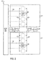
- FIG. 2 is a block diagram of another embodiment of the present invention.
- Memory array 200 is substantially similar to memory array 100 of Figure 1, and items numbered with 2xx numbers in Figure 2 are meant to correspond to items numbered with 1xx numbers in Figure 1.
- memory array 200 is comprised of address decoder 220, coupled to memory cell 260 within top half 210 by word line 230, and coupled to memory cell 262 within bottom half 212 by word line 232.
- memory cells 260 and 262 are each connected to a pair of bit lines (bit lines 270 and 274, and bit lines 272 and 276, respectively).
- pairs of bit lines are used with each memory cell to write and read both a bit of data and its complement to and from each memory cell.
- two (or more) bit lines are used to provide two (or more) entirely independent routes by which data may be written to or read from each memory cell. This use of the bit lines in this alternate embodiment would often reflects the way in which a multiple port memory component is often implemented.
- bit lines 270 and 272 are connected to the inputs of comparator circuit 240, and bit lines 274 and 276 are connected to the inputs of comparator circuit 244. Also corresponding to Figure 1, the outputs of comparator circuits 240 and 244 are connected to latches 242 and 246.
- memory cells 260 and 262 are tested by first writing identical data to each of memory cells 260 and 262 through bit lines 270 and 274, and bit lines 272 and 276, respectively.
- Bit lines 270 through 276 are then precharged to either a high voltage state or a low voltage state.
- Address decoder 220 then decodes part of a memory address associated with memory cells 260 and 262.
- Memory cells 260 and 262 then output their data onto bit lines 270 and 274, and bit lines 272 and 276, respectively.
- Comparator circuit 240 is a single comparator that continuously compares the voltages on bit lines 270 and 272, and continuously generates a signal indicating whether or not the voltages on bit lines 270 and 272 are substantially similar. Comparator circuit 244 does the same with the voltages on bit lines 274 and 276.
- latches 242 and 246 may be triggered at one or more predetermined times during the test to capture the state of the output of comparator circuits 240 and 244 at those times.
- latches 242 and 246 could each be implemented as a "sticky latch" that latches and stores any occurrence of a signal from the comparator circuits to which they are connected indicating that voltages on their associated bit lines became substantially different.
- the sense amplifiers could also be configured to serve as the comparators used as the comparator circuits to test the memory cells. This could be accomplished through the use of multiplexers to selectively connect and disconnect different ones of the bit lines as needed to allow the sense amplifiers to perform one or the other of these two functions. Otherwise, in an alternate embodiment, the sense amplifiers and the comparators could remain separate components.
- memory cells may be independently written to or read from using either of the bit lines attached to each of the memory cells, as in the case of a multiple port memory
- the memory cells are tested in much the same manner just described.
- the testing of each of memory cells 260 and 262 would be carried out twice, first using bit lines 270 and 272 to write identical data to memory cells 260 and 262, respectively, and then again using bit lines 274 and 276.
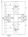
- FIG. 3 is a block diagram of yet another embodiment of the present invention.
- Memory array 300 is substantially similar to memory array 200 of Figure 2, and items numbered with 3xx numbers in Figure 3 are meant to correspond to items numbered with 2xx numbers in Figure 2, with exception of the comparator circuits and their associated latches.
- memory array 300 is comprised of address decoder 320, coupled to memory cell 360 within top half 310 by word line 330, and coupled to memory cell 362 within bottom half 312 by word line 332.
- memory cell 360 is coupled to bit lines 370 and 374
- memory cell 362 is coupled to bit lines 372 and 376.
- the comparator circuits of Figure 3 are each comprised of a subtracting circuit and a pair of comparators.
- Bit lines 370 and 372 are connected to the inputs of subtracting circuit 390.
- Subtracting circuits 390 subtracts the voltage level of one of bit lines 370 from the voltage level of the other of bit lines 372, and outputs a voltage that represents the difference resulting from the subtraction, which could be either a positive or negative voltage output.
- This output of subtracting circuit 390 is, in turn, connected to one of the two inputs on each of comparators 340 and 341.
- bit lines 374 and 376 are connected to the inputs of subtracting circuit 392, and the output of subtracting circuit 392 is connected to one of the two inputs on each of comparators 344 and 345.
- the other input on each of comparators 340 and 344 are connected to a high voltage level reference, +vref, and correspondingly, the other input on each of comparators 341 and 345 are connected to a low voltage reference, -vref.
- the outputs of comparators 340, 341, 344 and 345 are connected to the inputs of latches 342, 343, 346 and 347, respectively.
- the testing of memory cells 360 and 362 of memory array 300 is carried out in much the same way as was described above for memory cells 260 and 262 in Figure 2.
- the configuration of comparator circuits that are each comprised of a subtracting circuit and a pair of comparators as shown in Figure 3 affords greater ability to control the degree to which the voltages on pairs of bit lines that are being compared may differ from each other.
- comparators 340 and 344 can be biased to allow the voltage levels on bit lines 370 and 372 to differ to a degree that is adjustable before either comparator 340 or 344 outputs a signal indicating a malfunction. If the difference in voltage levels between bit lines 370 and 372 is such that it rises above +vref, then comparator 340 will output a signal indicating so to latch 342, and if the difference in voltages levels between bit lines 370 and 372 is such that it drops below -vref, then comparator 344 will output a signal indicating so to latch 346.
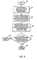
- FIG. 4 is a flow chart of one embodiment of the present invention.
- identical values are written to a pair of memory cells in a memory array at 410.
- corresponding pairs of bit lines from each of the two memory cells are connected to the inputs of a comparator circuit.
- each memory cell is connected to only one bit line, this would mean that each of the two bit lines would be connected to the inputs of a single comparator circuit at 420.
- each bit line from one memory cell is connected to a comparator circuit along with a corresponding bit line from the other memory cell at 420.
- the identical values are read back from each of the pair of memory cells, and each corresponding pair of bit lines connected to a comparator circuit are compared. If the voltage levels differ substantially between a corresponding pair of bit lines, then a failure is found at 460. However, if there are no substantially differing voltage levels between corresponding pairs of bit lines, then this test of the pair of memory cells and the bit lines to which they are connected passes at 450.
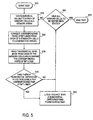
- Figure 5 is a flow chart of another embodiment of the present invention.
- the testing of memory cells in a memory array starts at 500.
- identical values are written to a pair of memory cells in a memory array, and at 520, corresponding pairs of bit lines coupled to each memory cell in the pair of memory cells are connected to the inputs of a comparator circuit.
- the identical values are read back from the pair of memory cells, and the voltage levels of the corresponding pairs of bit lines are compared.
- test may be repeated for memory cells 160 and 162, with bit lines 170 and 172 being pre-charged to a high state for one test of reading back the identical data, and then being pre-charged to a low state for another reading back of the identical data.
- bit lines 270 and 272 are used to write and read data
- bit lines 274 and 276 are used to write and read the complements of the data.
- identical values are written to memory cells 260 and 262, using bit lines 270 and 272 to write identical data to memory cells 260 and 262, respectively, while bit lines 274 and 276 are used to write identical complement data to memory cells 260 and 262, respectively.
- bit lines 270 and 272 are connected to the inputs of comparator circuit 240, and bit lines 274 and 276 are connected to the inputs of comparator circuit 244.
- the identical data and complements written to both memory cells 260 and 262 is read back using bit lines 270 and 274 to read back from memory cell 260, and bit lines 272 and 276 to read back from memory cell 262. If comparator circuit 240 detects a substantial difference in voltage between bit lines 270 and 272 while reading back the data, then an indication of this fact is latched by latch 242. Correspondingly, if comparator circuit 244 detects a substantial difference in voltage between bit lines 274 and 276 while reading back complement data, then an indication of this fact is latched by latch 244. If, at 560, more memory cells are to be tested, then at 510, another pair of identical values are written to another pair of memory cells. Alternatively, the test may be repeated for memory cells 260 and 262, with bit lines 270, 272, 274 and 276 being pre-charged to a high state for one test, and then being pre-charged to a low state for the other test.
- Figure 6 is a flow chart of still another embodiment of the present invention.
- the testing of memory cells using pairs of bit lines to read and write both bits of data and their complements in a memory array starts at 600.
- identical values are written to a pair of memory cells in a memory array, and at 620, corresponding ones of bit lines for data and complementary data that are coupled to each memory cell in the pair of memory cells are connected to the inputs of comparator circuits.
- voltage references used by the comparator circuits are set.
- the identical values are read back from the pair of memory cells, and the voltage levels of the corresponding pairs of bit lines for data and their complements are compared.
- the test ends if there are no more memory cells to be tested at 670. Otherwise, the test is repeated for another pair of memory cells at 610. Alternatively, the test may also be repeated if it is desired to test the bit lines with both a high and a low pre-charging during the reading back of the identical data.
- bit lines 370 and 372 are used to write and read data
- bit lines 374 and 376 are used to write and read the complements of the data.
- identical values are written to memory cells 360 and 362, using bit lines 370 and 372 to write identical data to memory cells 360 and 362, respectively, while bit lines 374 and 376 are used to write identical complement data to memory cells 360 and 362, respectively.
- bit lines 370 and 372 are connected to the inputs of subtracting circuit 390, which together with comparators 340 and 341, comprise a comparator circuit.
- bit lines 374 and 376 are connected to the inputs of subtracting circuit 392, which together with comparators 344 and 345, also comprise a comparator circuit.
- voltage reference +vref which is coupled to inputs of comparators 340 and 341
- voltage reference -vref which is coupled to inputs of comparators 344 and 345
- subtractor circuit 390 subtracts the voltage on bit line 370 from bit line 372, and outputs a voltage representing the resulting difference to the inputs of both comparators 340 and 341. If there is a difference in the voltage levels between bit lines 370 and 372, then the output of subtractor circuit 390 will be a non-zero voltage level that will be either negative or positive depending on which of bit lines 370 or 372 have the higher voltage level. Comparator 340 compares this output from subtracting circuit 390, if the voltage level of the output is higher than +vref, then an indication that this is so is latched by latch 342.
- comparator 341 compares the output from subtracting circuit 390, and if the voltage level of the output is lower than -vref, then an indication that this is so is latched by latch 343.
- subtracting circuit 392 provides an output representing the difference between the voltage levels of bit lines 374 and 376 to the inputs of comparators 344 and 345, which in turn, compare this output to +vref and -vref, respectively, and any indication that the voltage level of this output has risen above +vref or dropped below -vref is latched by latches 346 and 347, respectively.
- test may be repeated for memory cells 360 and 362, with bit lines 370, 372, 374 and 376 being pre-charged to a high state for one test, and then being pre-charged to a low state for the other test.
- the present invention may be used in variety of electronic, nucroelectronic and micromechanical devices.
Abstract
Description
- The present invention is related to the use of structural testing techniques to speed the testing of a memory array beyond what is possible with conventional functional tests.
- As memory arrays commonly used in many electronic devices become increasingly larger and more densely packed, the test complexity increases exponentially, and so does the time required to thoroughly test the individual cells and other memory array components. As a result, manufacturing test processes take increasing longer to complete, as do efforts to debug the faults that are found.
- Common practice within the art is to make use of functional tests wherein various combinations of values are written to and read back from memory cells within a memory array. However, as both the rows and columns of memory cells within memory arrays continue to increase in size, the number of write and read operations required to adequately test the memory cells increases exponentially, and causes a corresponding exponential increase in the amount of time required to carry out such tests. This has prompted questions about engaging in making increasing tradeoffs between manufacturing throughput of parts and thoroughness of test coverage, increasing the likelihood that faulty memory arrays will be passed on to customers.
- Such functional tests also do not provide much in the way of information needed to trace the source of the failure. In essence, when it is found that a cell has returned a value other than what was last written to it, this result doesn't not provide an indication as to whether it was an address decoder fault, a data latch fault, a data line fault, a memory cell fault or a driver fault. Therefore, further tests are needed to isolate the fault within the memory array so that subsequent manufacturing yields may be improved, and as memory arrays continue to increase in size, the length of time required to perform these additional tests also increases.
- US-2002/0027816-A1 discloses an integrated memory having identical memory and reference cells, so that the behaviour of the memory cells and the reference cells is influenced in a same way by fluctuations in their manufacturing process. Reference information is supplied to the reference cells. A memory cell to be read is connected by a first bit line to a first input of a differential amplifier and a reference cell is connected by a second bit line to a second input of the differential amplifier. The differential amplifier amplifies the potential difference between the two bit lines. After reading, the data in the memory cell is rewritten by means of the differential amplifier in that the information amplified is simply stored in the memory cell. The reference cell is rewritten by applying a standard potential. A write access is carried out in a known manner by selecting an appropriate memory cell via word lines and transferring data from data lines to bit lines via the differential amplifier.
- DE-19908513-A1 discloses a parallel bit test circuit that receives a plurality of data sets from a memory cell array and generates a test result for each data set. That is, a plurality of bits is tested simultaneously, to shorten a time to test the memory cell array. The parallel bit test circuit includes a pair of comparison circuits and a pair of latch circuits. In a memory cell array, a sense amplifier amplifies a potential difference between a first bit line and a second bit line. In parallel test bit mode, two sets of column selection lines are selected at a same time causing two sets of N-bit data to be simultaneously provided to the parallel test circuit. The first comparison circuit receives the first data set and detects whether all the N-bits of data are at an equivalent logic state and generates a first test data signal accordingly. A second comparison circuit receives the second data set and detects whether all the N-bits of data are at an equivalent logic state and generates a second test data signal accordingly. The first and second test data signals are latched. The first test signal is output in synchronisation with a rising edge of an external clock and the second test signal is output with a falling edge of the external clock. Thus the second test data signal is output without interfering with the first test data signal. Thus two parallel bit test data signals can be output during a single period of an external clock which reduces by half a time required to test all the data stored in the memory cell array.
- According to a first aspect of the invention, there is provided an apparatus for testing a memory array as claimed in claim 1.
According to a second aspect of the invention, there is provided a method of testing a memory array as claimed in claim 14. Further embodiments are disclosed in the dependent claims. - The objects, features, and advantages of the present invention will be apparent to one skilled in the art in view of the following detailed description in which:
- Figure 1 is a block diagram of one embodiment of the present invention.
- Figure 2 is a block diagram of another embodiment of the present invention.
- Figure 3 is a block diagram of still another embodiment of the present invention.
- Figure 4 is a flow chart of one embodiment of the present invention.
- Figure 5 is a flow chart of another embodiment of the present invention.
- Figure 6 is a flow chart of still another embodiment of the present invention.
- In the following description, for purposes of explanation, numerous details are set forth in order to provide a thorough understanding of the present invention.
However, it will be apparent to one skilled in the art that these specific details are not required in order to practice the present invention.
The present invention concerns memory arrays in which there exists an array of memory cells organized in rows and columns, wherein the memory cells are dynamically and randomly accessible, as in the case of commonly available DRAM and SRAM ICs. However, as those skilled in the art will appreciate, the present invention is also applicable to arrays of other circuits, including but not limited to, erasable ROM ICs, programmable logic devices and components organized into arrays within microprocessors. - Figure 1 is a block diagram of one embodiment of the present invention.
Memory array 100 is depicted as comprised oftop half 110,bottom half 112, address decoder 120 connected to bothtop half 110 andbottom half 112 via a plurality of word lines (includingword lines 130 and 132),comparator circuit 140, andlatch 142. Withintop half 110 andbottom half 112 arememory cells bit lines Bit lines comparator circuit 140, which is in turn connected tolatch 142. For purposes of clarity in discussing of the present invention, onlymemory cell 160 andbit line 170 are shown intop half 100, and onlymemory cell 162 andbit line 172 are shown inbottom half 112. However, as known by those skilled in the art, a typical memory array will have many bit lines, each of which will have many memory cells connected to it. - During normal operation of
memory array 100, address decoder 120 decodes part of a memory address and turns on appropriate ones of the word lines connecting address decoder 120 withtop half 110 andbottom half 112 to enable access to appropriate memory cells withintop half 110 andbottom half 112. Depending on the memory operation being performed, data is either written to or read from memory cells intop half 110 andbottom half 112 via the bit lines to which they are connected. For example, during a write operation to a memory address associated with bothmemory cells word lines memory cells bit lines - In one embodiment of the present invention,
memory cells memory cells bit lines Bit lines memory cells Memory cells bit lines Comparator circuit 140 is a single comparator that continuously compares the voltages onbit lines bit lines latch 142 may be triggered at one or more predetermined times during the test to capture the state of the output ofcomparator circuit 140 at such times, such as example times t1 and t2 during the progress ofexample waveforms bit lines latch 142 could be implemented as a "sticky latch" that latches and stores any occurrence of a signal fromcomparator circuit 140 indicating that the voltages onbit lines - It is common practice when reading memory cells during normal use of a memory array to precharge the bit lines to a high voltage state. Therefore, in one embodiment of the present invention, the testing of the memory cells would be carried out with the bit lines being charged only to a high state when reading the memory cells. However, due to commonly used memory cell designs, limiting precharging to only a high state would result in as much as half of the circuitry of a memory cell not being tested for excessive leakage or other conditions. Therefore, another embodiment of the present invention would entail testing with the bit lines precharged to both high and low states.
- The use of
comparator circuit 140 to testmemory cells bit lines 170 and 172 (such asexample waveforms 180 and 182) should look substantially similar. This use of a comparator circuit is also based on the assumption of it being highly unlikely that a process variation or other defect inmemory array 100 will result in identical faults to bothtop half 110 andbottom half 112, and so it is highly unlikely that bothmemory cells bit lines top half 110 andbottom half 112 such that tests carried out in accordance with the present invention will reveal no differences between any pair of memory cells betweentop half 110 andbottom half 112. -
Memory array 100 is shown as split intotop half 110 andbottom half 112 in accordance with a common practice known to those skilled in the art so that buffers and other associated circuitry may be centrally located, and allowing the bit lines to be kept short to give the bit lines more desirable electrical characteristics. The present invention takes advantage of this common practice to make use of the same central location provided to centrally locate comparator circuits, such ascomparator 140, to compare the electrical characteristics of adjacent bit lines. However, as will also be clear to those skilled in the art, this split ofmemory array 100 intotop half 110 andbottom half 112 is not necessary to the practice of the present invention. The present invention may be practiced with numerous other layouts or placements of the components comprising a memory array. - Figure 2 is a block diagram of another embodiment of the present invention.
Memory array 200 is substantially similar tomemory array 100 of Figure 1, and items numbered with 2xx numbers in Figure 2 are meant to correspond to items numbered with 1xx numbers in Figure 1. In a manner corresponding tomemory array 100,memory array 200 is comprised ofaddress decoder 220, coupled to memory cell 260 withintop half 210 byword line 230, and coupled tomemory cell 262 withinbottom half 212 by word line 232. - However, unlike
memory cells memory cells 260 and 262 are each connected to a pair of bit lines (bit lines lines - Regardless of the purpose for having a pair of bit lines connected to each of
memory cells 260 and 262, in a manner that corresponds to bitlines memory array 100 of Figure 1,bit lines comparator circuit 240, and bitlines comparator circuit 244. Also corresponding to Figure 1, the outputs ofcomparator circuits - In an embodiment of the present invention where memory cells are written to and read from using pairs of bit lines that carry data and its complement,
memory cells 260 and 262 are tested by first writing identical data to each ofmemory cells 260 and 262 throughbit lines lines Bit lines 270 through 276 are then precharged to either a high voltage state or a low voltage state.Address decoder 220 then decodes part of a memory address associated withmemory cells 260 and 262.Memory cells 260 and 262 then output their data ontobit lines lines Comparator circuit 240 is a single comparator that continuously compares the voltages onbit lines bit lines Comparator circuit 244 does the same with the voltages onbit lines comparator circuits - Furthermore, in an embodiment where memory cells are written to and read from using pairs of bit lines to carry data and its complement and sense amplifiers are used in reading from memory cells, the sense amplifiers could also be configured to serve as the comparators used as the comparator circuits to test the memory cells. This could be accomplished through the use of multiplexers to selectively connect and disconnect different ones of the bit lines as needed to allow the sense amplifiers to perform one or the other of these two functions. Otherwise, in an alternate embodiment, the sense amplifiers and the comparators could remain separate components.
- In an alternate embodiment of the present invention where memory cells may be independently written to or read from using either of the bit lines attached to each of the memory cells, as in the case of a multiple port memory, the memory cells are tested in much the same manner just described. However, to ensure that the function of writing
memory cells 260 and 262 is free of defects, the testing of each ofmemory cells 260 and 262 would be carried out twice, first usingbit lines memory cells 260 and 262, respectively, and then again usingbit lines - Figure 3 is a block diagram of yet another embodiment of the present invention.
Memory array 300 is substantially similar tomemory array 200 of Figure 2, and items numbered with 3xx numbers in Figure 3 are meant to correspond to items numbered with 2xx numbers in Figure 2, with exception of the comparator circuits and their associated latches. In a manner corresponding tomemory array 200,memory array 300 is comprised ofaddress decoder 320, coupled to memory cell 360 withintop half 310 byword line 330, and coupled tomemory cell 362 withinbottom half 312 byword line 332. Also in a manner corresponding tomemory array 200, memory cell 360 is coupled tobit lines memory cell 362 is coupled tobit lines - Unlike the embodiment depicted in Figure 2, the comparator circuits of Figure 3 are each comprised of a subtracting circuit and a pair of comparators.
Bit lines circuit 390. Subtractingcircuits 390 subtracts the voltage level of one ofbit lines 370 from the voltage level of the other ofbit lines 372, and outputs a voltage that represents the difference resulting from the subtraction, which could be either a positive or negative voltage output. This output of subtractingcircuit 390 is, in turn, connected to one of the two inputs on each ofcomparators bit lines circuit 392, and the output of subtractingcircuit 392 is connected to one of the two inputs on each ofcomparators comparators comparators comparators latches - Regardless of whether the memory cells of
memory array 300 are written to and read from with a pair of bit lines, or each of the two bit lines connected to each cell are meant to be used to perform independent read and write operations, the testing ofmemory cells 360 and 362 ofmemory array 300 is carried out in much the same way as was described above formemory cells 260 and 262 in Figure 2. However, the configuration of comparator circuits that are each comprised of a subtracting circuit and a pair of comparators as shown in Figure 3 affords greater ability to control the degree to which the voltages on pairs of bit lines that are being compared may differ from each other. More precisely, by adjusting +vref and -vref,comparators bit lines comparator bit lines bit lines - Figure 4 is a flow chart of one embodiment of the present invention. Starting at 400, identical values are written to a pair of memory cells in a memory array at 410. At 420, corresponding pairs of bit lines from each of the two memory cells are connected to the inputs of a comparator circuit. In one embodiment, where each memory cell is connected to only one bit line, this would mean that each of the two bit lines would be connected to the inputs of a single comparator circuit at 420. Alternatively, in another embodiment where each memory cell is connected to two bit lines, then each bit line from one memory cell is connected to a comparator circuit along with a corresponding bit line from the other memory cell at 420.
- At 430, the identical values are read back from each of the pair of memory cells, and each corresponding pair of bit lines connected to a comparator circuit are compared. If the voltage levels differ substantially between a corresponding pair of bit lines, then a failure is found at 460. However, if there are no substantially differing voltage levels between corresponding pairs of bit lines, then this test of the pair of memory cells and the bit lines to which they are connected passes at 450.
- Figure 5 is a flow chart of another embodiment of the present invention. The testing of memory cells in a memory array starts at 500. At 510, identical values are written to a pair of memory cells in a memory array, and at 520, corresponding pairs of bit lines coupled to each memory cell in the pair of memory cells are connected to the inputs of a comparator circuit. Then, at 530, the identical values are read back from the pair of memory cells, and the voltage levels of the corresponding pairs of bit lines are compared. If, at 540, a substantial difference is found in the voltage levels in a corresponding pair of bit lines, then the fact that a substantial difference was found is latched at 550, However, regardless of whether such a substantial difference was found at 540, the test ends if there are no more memory cells to be tested at 560. Otherwise, the test is repeated for another pair of memory cells at 510.
- By way of one example, referring variously to both Figures 1 and 5, at 510, identical values are written to
memory cells bit lines bit lines comparator circuit 140. At 530, the identical data written to bothmemory cells memory cells bit lines bit lines comparator circuit 140. Ifcomparator circuit 140 detects a substantial difference in voltage betweenbit lines latch 142. If, at 560, more memory cells are to be tested, then at 510, another pair of identical values are written to another pair of memory cells. Alternatively, the test may be repeated formemory cells bit lines - By way of another example, referring variously to both Figures 2 and 5, where
memory cells 260 and 262 are written to and read from with pairs of bit lines, and specifically, wherebit lines bit lines memory cells 260 and 262, usingbit lines memory cells 260 and 262, respectively, whilebit lines memory cells 260 and 262, respectively. At 520,bit lines comparator circuit 240, and bitlines comparator circuit 244. At 530, the identical data and complements written to bothmemory cells 260 and 262 is read back usingbit lines lines memory cell 262. Ifcomparator circuit 240 detects a substantial difference in voltage betweenbit lines latch 242. Correspondingly, ifcomparator circuit 244 detects a substantial difference in voltage betweenbit lines latch 244. If, at 560, more memory cells are to be tested, then at 510, another pair of identical values are written to another pair of memory cells. Alternatively, the test may be repeated formemory cells 260 and 262, withbit lines - Figure 6 is a flow chart of still another embodiment of the present invention. The testing of memory cells using pairs of bit lines to read and write both bits of data and their complements in a memory array starts at 600. At 610, identical values are written to a pair of memory cells in a memory array, and at 620, corresponding ones of bit lines for data and complementary data that are coupled to each memory cell in the pair of memory cells are connected to the inputs of comparator circuits. Then, at 630, voltage references used by the comparator circuits are set. At 640, the identical values are read back from the pair of memory cells, and the voltage levels of the corresponding pairs of bit lines for data and their complements are compared. If, at 650, a substantial difference is found in the voltage levels in a corresponding pair of bit lines, then the fact that a substantial difference was found is latched at 660, However, regardless of whether such a substantial difference was found at 650, the test ends if there are no more memory cells to be tested at 670. Otherwise, the test is repeated for another pair of memory cells at 610. Alternatively, the test may also be repeated if it is desired to test the bit lines with both a high and a low pre-charging during the reading back of the identical data.
- By way of example, referring variously to both Figures 3 and 6, where
memory cells 360 and 362 are written to and read from with pairs of bit lines, and specifically, wherebit lines bit lines memory cells 360 and 362, usingbit lines memory cells 360 and 362, respectively, whilebit lines memory cells 360 and 362, respectively. At 620,bit lines circuit 390, which together withcomparators bit lines circuit 392, which together withcomparators comparators comparators memory cells 360 and 362 is read back, usingbit lines lines memory cell 262. At 650, if a substantial difference was found in the voltage levels of corresponding pairs ofbit lines bit lines latches - More specifically,
subtractor circuit 390 subtracts the voltage onbit line 370 frombit line 372, and outputs a voltage representing the resulting difference to the inputs of bothcomparators bit lines subtractor circuit 390 will be a non-zero voltage level that will be either negative or positive depending on which ofbit lines Comparator 340 compares this output from subtractingcircuit 390, if the voltage level of the output is higher than +vref, then an indication that this is so is latched bylatch 342. Similarly,comparator 341 compares the output from subtractingcircuit 390, and if the voltage level of the output is lower than -vref, then an indication that this is so is latched bylatch 343. Correspondingly, subtractingcircuit 392 provides an output representing the difference between the voltage levels ofbit lines comparators latches - If, at 670, more memory cells are to be tested, then at 610, another pair of identical values are written to another pair of memory cells. Alternatively, the test may be repeated for
memory cells 360 and 362, withbit lines - The invention has been described in conjunction with the preferred embodiment. It is evident that numerous alternatives, modifications, variations and uses will be apparent to those skilled in the art in light of the foregoing description.
- The present invention may be used in variety of electronic, nucroelectronic and micromechanical devices.
Claims (16)
- An apparatus for testing a memory array, comprising an address decoder (220) coupled to a first memory cell (260, 360) and a second memory cell (262, 362) to enable access to the first and second memory cells, the apparatus characterized by:the first memory cell (260, 360) concurrently coupled to a first bit line (270, 370) and a second bit line (274, 374);the second memory cell (262, 362) concurrently coupled to a third bit line (272, 372) and a fourth bit line (276, 376);a first comparator circuit (240; 340, 341, 390) coupled to the first (270, 370) and third (272, 372) bit lines to compare a voltage level on the first bit line (270, 370) with a voltage level on the third bit line (272, 372) at a time when data is output from the first memory cell (260, 360) on the first bit line (270, 370) and from the second memory cell (262, 362) on the third bit line (272, 372); anda second comparator circuit (244; 344, 345, 392) coupled to the second (274, 374) and fourth (276, 376) bit lines to compare a voltage level on the second bit line (274, 374) with a voltage level on the fourth bit line (276, 376) at a time when the complement of the data that is output on the first (270, 370) and third (272, 372) bit lines is output from the first memory cell (260, 360) on the second bit line (274, 374) and from the second memory cell on the fourth bit line (276, 376).
- The apparatus of claim 1, wherein the address decoder (220) decodes part of a memory address.
- The apparatus of claim 1, wherein the first (260, 360) and second (262, 362) memory cells are dynamic RAM memory cells.
- The apparatus of claim 1, wherein the first (260, 360) and second (262, 362) memory cells are static RAM memory cells.
- The apparatus of claim 1, wherein the first comparator circuit is comprised of a single comparator (240) with a first input coupled to the first bit line (270) and a second input coupled to the third bit line (272), and wherein the second comparator circuit is comprised of a single comparator (244) with a first input coupled to the second bit line (274) and a second input coupled to the fourth bit line (276).
- The apparatus of claim 5, wherein the output of the first comparator (240) is coupled to a first latch (242) to store an indication that the voltage level on the first bit line (270) differs substantially from the voltage level on the third bit line (272) and wherein the output of the second comparator (244) is coupled to a second latch (246) to store an indication that the voltage level on the second bit line (274) differs substantially from the voltage level on the fourth bit line (276).
- The apparatus of claim 6, wherein the time at which the first (242) and second (246) latches are triggered is adjustable.
- The apparatus of claim 6, wherein the first latch (242) is a sticky latch that is triggered to latch an indication that the voltage level on the first bit line (270) differs substantially from the voltage level on the third bit line (272), and wherein the second latch (246) is a sticky latch that is triggered to latch an indication that the voltage level on the second bit line (274) differs substantially from the voltage level on the fourth bit line (276).
- The apparatus of claim 1, wherein the first (340, 341, 390) and second (344, 345, 392) comparator circuits are each comprised of:a subtracting circuit (390, 392) with a first input coupled to a first input bit line (370, 374) and a second input coupled to a second input bit line (372, 376);a first comparator (340, 344) coupled to the output of the subtracting circuit (390, 392); anda second comparator (341, 345) coupled to the output of the subtracting circuit (390, 392).
- The apparatus of claim 9, wherein:the output of the first comparator (340, 344) is coupled to a first latch (342, 346) to store an indication that difference in voltage levels between the first input bit line (370, 374) and the second input bit line (372, 376) has risen above a first reference voltage (+VREF); andthe output of the second comparator (341, 345) is coupled to a second latch (343, 347) to store an indication that the difference in voltage levels between the first input bit line (370, 374) and the second input bit line (372, 376) has dropped below a second reference voltage (-VREF).
- The apparatus of claim 10, wherein the first (+VREF) and second (-VREF) reference voltages are adjustable.
- The apparatus of claim 10, wherein the time at which the first (342, 346) and second (343, 347) latches are triggered is adjustable.
- The apparatus of claim 10, wherein the first (342, 346) and second (343, 347) latches are sticky latches such that the first latch (342, 346) will latch any indication that the differences in voltage level between the first (370, 374) and second (372, 376) input bit lines has risen above the first voltage reference (+VREF) and the second latch (343, 347) will latch any indication that the differences in voltage level between the first (370, 374) and second (372, 376) input bit lines has dropped below the second reference voltage (-VREF).
- A method of testing a memory array, comprising:coupling a first memory cell (260, 360) concurrently to a first bit line (270, 370);coupling a second memory cell (262, 362) concurrently to a third bit line (272, 372); the method characterized in that:writing identical values to the first (260, 360) and second (262, 362) memory cells;coupling the first memory cell (260, 360) to a second bit line (274, 374);coupling the second memory cell (262, 362) to a fourth bit line (276, 376);coupling the first (270, 370) and third bit lines (272, 372) to inputs of a first comparator circuit (240; 340, 341,390);coupling the second (274, 374) and fourth (276, 376) bit lines to inputs of a second comparator circuit (244; 344, 345, 392);reading the identical values from the first memory cell (260, 360) through the first bit line (270, 370) and from the second memory cell (262, 362) through the third bit line (272, 372); reading the identical values from the first memory cell (260, 360) through the second bit line (274, 374) and from the second memory cell (262, 362) through the fourth bit line (276, 376) that are complements of the values read through the first (270, 370) and third (272, 372) bit lines;comparing the voltage levels on the first (270, 370) and third(272, 372) bit lines; andcomparing the voltage levels on the second (274, 374) and fourth (276, 376) bit lines.
- The method of claim 14, further comprising latching an indication from the first comparator circuit (240; 340, 341, 390) of whether or not the voltage level of the first bit line (270, 370) differs substantially from the voltage level of the third bit line (272, 372), and latching an indication from the second comparator circuit (244; 344, 345, 392) of whether or not the voltage level of the second bit line (274, 374) differs substantially from the voltage level of the fourth bit line (276, 376).
- The method of claim 14, further comprising setting the degree to which the difference in voltage levels between the first bit line (270, 370) and the third bit line(272, 372), and between the second bit line (274, 374) and the fourth bit line (276, 376) are substantial.
Applications Claiming Priority (3)
| Application Number | Priority Date | Filing Date | Title |
|---|---|---|---|
| US823642 | 2001-03-30 | ||
| US09/823,642 US6757209B2 (en) | 2001-03-30 | 2001-03-30 | Memory cell structural test |
| PCT/US2002/007340 WO2002080183A2 (en) | 2001-03-30 | 2002-03-08 | Memory cell structural test |
Publications (2)
| Publication Number | Publication Date |
|---|---|
| EP1374250A2 EP1374250A2 (en) | 2004-01-02 |
| EP1374250B1 true EP1374250B1 (en) | 2006-06-07 |
Family
ID=25239313
Family Applications (1)
| Application Number | Title | Priority Date | Filing Date |
|---|---|---|---|
| EP02717602A Expired - Lifetime EP1374250B1 (en) | 2001-03-30 | 2002-03-08 | Memory cell structural test |
Country Status (10)
| Country | Link |
|---|---|
| US (1) | US6757209B2 (en) |
| EP (1) | EP1374250B1 (en) |
| JP (1) | JP2004530243A (en) |
| KR (1) | KR100544362B1 (en) |
| CN (1) | CN100538910C (en) |
| AT (1) | ATE329354T1 (en) |
| DE (1) | DE60212103T2 (en) |
| HK (1) | HK1060437A1 (en) |
| MY (1) | MY127555A (en) |
| WO (1) | WO2002080183A2 (en) |
Families Citing this family (7)
| Publication number | Priority date | Publication date | Assignee | Title |
|---|---|---|---|---|
| US7480195B2 (en) * | 2005-05-11 | 2009-01-20 | Micron Technology, Inc. | Internal data comparison for memory testing |
| US7602778B2 (en) * | 2005-06-29 | 2009-10-13 | Cisco Technology, Inc. | System and methods for compressing message headers |
| JP4773791B2 (en) * | 2005-09-30 | 2011-09-14 | 富士通セミコンダクター株式会社 | Semiconductor memory device and memory test circuit |
| US7548473B2 (en) * | 2006-04-14 | 2009-06-16 | Purdue Research Foundation | Apparatus and methods for determining memory device faults |
| CN101714407B (en) * | 2009-11-12 | 2012-08-08 | 钰创科技股份有限公司 | Row address reserved storage location trigger circuit and row address reserved storage location device |
| JP6430194B2 (en) * | 2014-09-29 | 2018-11-28 | ルネサスエレクトロニクス株式会社 | Semiconductor memory device |
| CN108051767B (en) * | 2018-01-04 | 2019-07-19 | 南京国睿安泰信科技股份有限公司 | A kind of automatic diagnosis method for integrated circuit tester |
Family Cites Families (24)
| Publication number | Priority date | Publication date | Assignee | Title |
|---|---|---|---|---|
| JPS57105897A (en) * | 1980-12-23 | 1982-07-01 | Fujitsu Ltd | Semiconductor storage device |
| US4503536A (en) | 1982-09-13 | 1985-03-05 | General Dynamics | Digital circuit unit testing system utilizing signature analysis |
| US4527272A (en) | 1982-12-06 | 1985-07-02 | Tektronix, Inc. | Signature analysis using random probing and signature memory |
| JPS61261895A (en) * | 1985-05-16 | 1986-11-19 | Toshiba Corp | Semiconductor memory device |
| JPS61292300A (en) * | 1985-06-18 | 1986-12-23 | Toshiba Corp | Facilitating circuit for on-chip memory test |
| JP2523586B2 (en) * | 1987-02-27 | 1996-08-14 | 株式会社日立製作所 | Semiconductor memory device |
| JP2831767B2 (en) * | 1990-01-10 | 1998-12-02 | 株式会社アドバンテスト | Semiconductor memory test equipment |
| JPH04212799A (en) * | 1990-01-31 | 1992-08-04 | Nec Ic Microcomput Syst Ltd | Semiconductor memory built in test circuit |
| JPH04211160A (en) * | 1990-03-20 | 1992-08-03 | Mitsubishi Electric Corp | Semiconductor memory |
| KR940007240B1 (en) * | 1992-02-21 | 1994-08-10 | 현대전자산업 주식회사 | Parallel test circuit |
| JP3251637B2 (en) * | 1992-05-06 | 2002-01-28 | 株式会社東芝 | Semiconductor storage device |
| JP3307473B2 (en) * | 1992-09-09 | 2002-07-24 | ソニー エレクトロニクス インコーポレイテッド | Test circuit for semiconductor memory |
| JPH07211099A (en) * | 1994-01-12 | 1995-08-11 | Sony Corp | Semiconductor storage device testing apparatus |
| JPH07307100A (en) * | 1994-05-11 | 1995-11-21 | Nec Corp | Memory integrated circuit |
| US5708598A (en) * | 1995-04-24 | 1998-01-13 | Saito; Tamio | System and method for reading multiple voltage level memories |
| JP3607407B2 (en) * | 1995-04-26 | 2005-01-05 | 株式会社日立製作所 | Semiconductor memory device |
| US5973967A (en) * | 1997-01-03 | 1999-10-26 | Programmable Microelectronics Corporation | Page buffer having negative voltage level shifter |
| US6002623A (en) * | 1997-02-12 | 1999-12-14 | Micron Technology, Inc. | Semiconductor memory with test circuit |
| JPH10308100A (en) | 1997-05-06 | 1998-11-17 | Mitsubishi Electric Corp | Semiconductor memory device |
| KR100269319B1 (en) | 1997-12-29 | 2000-10-16 | 윤종용 | Semiconductor memory device including simultaneous enabling circuit for column select line and control method |
| US5963497A (en) * | 1998-05-18 | 1999-10-05 | Silicon Aquarius, Inc. | Dynamic random access memory system with simultaneous access and refresh operations and methods for using the same |
| KR100308191B1 (en) | 1998-05-28 | 2001-11-30 | 윤종용 | Semiconductor memory device having built-in parallel test circuit |
| JP2001210095A (en) * | 2000-01-24 | 2001-08-03 | Mitsubishi Electric Corp | Memory module |
| US6353568B1 (en) * | 2000-12-29 | 2002-03-05 | Lsi Logic Corporation | Dual threshold voltage sense amplifier |
-
2001
- 2001-03-30 US US09/823,642 patent/US6757209B2/en not_active Expired - Fee Related
-
2002
- 2002-01-21 MY MYPI20020232A patent/MY127555A/en unknown
- 2002-03-08 JP JP2002578510A patent/JP2004530243A/en not_active Ceased
- 2002-03-08 KR KR1020037012883A patent/KR100544362B1/en not_active IP Right Cessation
- 2002-03-08 CN CNB028106474A patent/CN100538910C/en not_active Expired - Fee Related
- 2002-03-08 EP EP02717602A patent/EP1374250B1/en not_active Expired - Lifetime
- 2002-03-08 WO PCT/US2002/007340 patent/WO2002080183A2/en active IP Right Grant
- 2002-03-08 DE DE60212103T patent/DE60212103T2/en not_active Expired - Fee Related
- 2002-03-08 AT AT02717602T patent/ATE329354T1/en not_active IP Right Cessation
-
2004
- 2004-05-13 HK HK04103384A patent/HK1060437A1/en not_active IP Right Cessation
Also Published As
| Publication number | Publication date |
|---|---|
| DE60212103D1 (en) | 2006-07-20 |
| WO2002080183A3 (en) | 2003-04-17 |
| CN1537312A (en) | 2004-10-13 |
| HK1060437A1 (en) | 2004-08-06 |
| EP1374250A2 (en) | 2004-01-02 |
| DE60212103T2 (en) | 2007-01-04 |
| CN100538910C (en) | 2009-09-09 |
| KR100544362B1 (en) | 2006-01-23 |
| ATE329354T1 (en) | 2006-06-15 |
| US20020141259A1 (en) | 2002-10-03 |
| WO2002080183A2 (en) | 2002-10-10 |
| MY127555A (en) | 2006-12-29 |
| KR20030085084A (en) | 2003-11-01 |
| JP2004530243A (en) | 2004-09-30 |
| US6757209B2 (en) | 2004-06-29 |
Similar Documents
| Publication | Publication Date | Title |
|---|---|---|
| US5060230A (en) | On chip semiconductor memory arbitrary pattern, parallel test apparatus and method | |
| US6816422B2 (en) | Semiconductor memory device having multi-bit testing function | |
| US7298655B2 (en) | Isolation control circuit and method for a memory device | |
| US6501692B1 (en) | Circuit and method for stress testing a static random access memory (SRAM) device | |
| US5343429A (en) | Semiconductor memory device having redundant circuit and method of testing to see whether or not redundant circuit is used therein | |
| US8966329B2 (en) | Fast parallel test of SRAM arrays | |
| US6590818B1 (en) | Method and apparatus for soft defect detection in a memory | |
| JPH04228200A (en) | Short-circuit detector circuit for memory array | |
| KR100367191B1 (en) | Memory IDDQ-testable through cumulative word line activation | |
| EP1374250B1 (en) | Memory cell structural test | |
| KR950005578B1 (en) | Circuit configuration and method for the testing of storage cells | |
| KR100518579B1 (en) | Semiconductor device and test method there-of | |
| US7474573B2 (en) | Semiconductor memory device capable of writing different data in cells coupled to one word line during burn-in test | |
| US20070127300A1 (en) | Bun-in test method semiconductor memory device | |
| US7388796B2 (en) | Method for testing memory under worse-than-normal conditions | |
| US9001568B2 (en) | Testing signal development on a bit line in an SRAM | |
| JPH0589700A (en) | Mechanism of high-speed parallel test | |
| US20190341121A1 (en) | Testing method for reading current of static random access memory | |
| KR100399450B1 (en) | Method of inspecting semiconductor memory device | |
| KR19980069836A (en) | Semiconductor memory | |
| JPH0729375A (en) | Semiconductor storage device | |
| KR100244455B1 (en) | Reference voltage generation circuit of sense amplifier using remnant data line | |
| KR100266648B1 (en) | Redundancy circuit in semiconductor integrated circuit | |
| JP2020123411A (en) | Semiconductor storage device and operation method thereof | |
| JP2011181142A (en) | Method of testing semiconductor memory device |
Legal Events
| Date | Code | Title | Description |
|---|---|---|---|
| PUAI | Public reference made under article 153(3) epc to a published international application that has entered the european phase |
Free format text: ORIGINAL CODE: 0009012 |
|
| 17P | Request for examination filed |
Effective date: 20031028 |
|
| AK | Designated contracting states |
Kind code of ref document: A2 Designated state(s): AT BE CH CY DE DK ES FI FR GB GR IE IT LI LU MC NL PT SE TR |
|
| AX | Request for extension of the european patent |
Extension state: AL LT LV MK RO SI |
|
| REG | Reference to a national code |
Ref country code: HK Ref legal event code: DE Ref document number: 1060437 Country of ref document: HK |
|
| 17Q | First examination report despatched |
Effective date: 20050518 |
|
| GRAP | Despatch of communication of intention to grant a patent |
Free format text: ORIGINAL CODE: EPIDOSNIGR1 |
|
| GRAS | Grant fee paid |
Free format text: ORIGINAL CODE: EPIDOSNIGR3 |
|
| GRAA | (expected) grant |
Free format text: ORIGINAL CODE: 0009210 |
|
| AK | Designated contracting states |
Kind code of ref document: B1 Designated state(s): AT BE CH CY DE DK ES FI FR GB GR IE IT LI LU MC NL PT SE TR |
|
| PG25 | Lapsed in a contracting state [announced via postgrant information from national office to epo] |
Ref country code: AT Free format text: LAPSE BECAUSE OF FAILURE TO SUBMIT A TRANSLATION OF THE DESCRIPTION OR TO PAY THE FEE WITHIN THE PRESCRIBED TIME-LIMIT Effective date: 20060607 Ref country code: CH Free format text: LAPSE BECAUSE OF FAILURE TO SUBMIT A TRANSLATION OF THE DESCRIPTION OR TO PAY THE FEE WITHIN THE PRESCRIBED TIME-LIMIT Effective date: 20060607 Ref country code: BE Free format text: LAPSE BECAUSE OF FAILURE TO SUBMIT A TRANSLATION OF THE DESCRIPTION OR TO PAY THE FEE WITHIN THE PRESCRIBED TIME-LIMIT Effective date: 20060607 Ref country code: IT Free format text: LAPSE BECAUSE OF FAILURE TO SUBMIT A TRANSLATION OF THE DESCRIPTION OR TO PAY THE FEE WITHIN THE PRESCRIBED TIME-LIMIT;WARNING: LAPSES OF ITALIAN PATENTS WITH EFFECTIVE DATE BEFORE 2007 MAY HAVE OCCURRED AT ANY TIME BEFORE 2007. THE CORRECT EFFECTIVE DATE MAY BE DIFFERENT FROM THE ONE RECORDED. Effective date: 20060607 Ref country code: FI Free format text: LAPSE BECAUSE OF FAILURE TO SUBMIT A TRANSLATION OF THE DESCRIPTION OR TO PAY THE FEE WITHIN THE PRESCRIBED TIME-LIMIT Effective date: 20060607 Ref country code: LI Free format text: LAPSE BECAUSE OF FAILURE TO SUBMIT A TRANSLATION OF THE DESCRIPTION OR TO PAY THE FEE WITHIN THE PRESCRIBED TIME-LIMIT Effective date: 20060607 |
|
| REG | Reference to a national code |
Ref country code: GB Ref legal event code: FG4D |
|
| REG | Reference to a national code |
Ref country code: CH Ref legal event code: EP |
|
| REG | Reference to a national code |
Ref country code: IE Ref legal event code: FG4D |
|
| REF | Corresponds to: |
Ref document number: 60212103 Country of ref document: DE Date of ref document: 20060720 Kind code of ref document: P |
|
| PG25 | Lapsed in a contracting state [announced via postgrant information from national office to epo] |
Ref country code: DK Free format text: LAPSE BECAUSE OF FAILURE TO SUBMIT A TRANSLATION OF THE DESCRIPTION OR TO PAY THE FEE WITHIN THE PRESCRIBED TIME-LIMIT Effective date: 20060907 Ref country code: SE Free format text: LAPSE BECAUSE OF FAILURE TO SUBMIT A TRANSLATION OF THE DESCRIPTION OR TO PAY THE FEE WITHIN THE PRESCRIBED TIME-LIMIT Effective date: 20060907 |
|
| PG25 | Lapsed in a contracting state [announced via postgrant information from national office to epo] |
Ref country code: ES Free format text: LAPSE BECAUSE OF FAILURE TO SUBMIT A TRANSLATION OF THE DESCRIPTION OR TO PAY THE FEE WITHIN THE PRESCRIBED TIME-LIMIT Effective date: 20060918 |
|
| PG25 | Lapsed in a contracting state [announced via postgrant information from national office to epo] |
Ref country code: PT Free format text: LAPSE BECAUSE OF FAILURE TO SUBMIT A TRANSLATION OF THE DESCRIPTION OR TO PAY THE FEE WITHIN THE PRESCRIBED TIME-LIMIT Effective date: 20061107 |
|
| REG | Reference to a national code |
Ref country code: HK Ref legal event code: GR Ref document number: 1060437 Country of ref document: HK |
|
| REG | Reference to a national code |
Ref country code: CH Ref legal event code: PL |
|
| PLBE | No opposition filed within time limit |
Free format text: ORIGINAL CODE: 0009261 |
|
| STAA | Information on the status of an ep patent application or granted ep patent |
Free format text: STATUS: NO OPPOSITION FILED WITHIN TIME LIMIT |
|
| EN | Fr: translation not filed | ||
| 26N | No opposition filed |
Effective date: 20070308 |
|
| PG25 | Lapsed in a contracting state [announced via postgrant information from national office to epo] |
Ref country code: MC Free format text: LAPSE BECAUSE OF NON-PAYMENT OF DUE FEES Effective date: 20070331 Ref country code: IE Free format text: LAPSE BECAUSE OF NON-PAYMENT OF DUE FEES Effective date: 20070308 |
|
| PG25 | Lapsed in a contracting state [announced via postgrant information from national office to epo] |
Ref country code: FR Free format text: LAPSE BECAUSE OF FAILURE TO SUBMIT A TRANSLATION OF THE DESCRIPTION OR TO PAY THE FEE WITHIN THE PRESCRIBED TIME-LIMIT Effective date: 20070309 Ref country code: GR Free format text: LAPSE BECAUSE OF FAILURE TO SUBMIT A TRANSLATION OF THE DESCRIPTION OR TO PAY THE FEE WITHIN THE PRESCRIBED TIME-LIMIT Effective date: 20060908 |
|
| PG25 | Lapsed in a contracting state [announced via postgrant information from national office to epo] |
Ref country code: FR Free format text: LAPSE BECAUSE OF FAILURE TO SUBMIT A TRANSLATION OF THE DESCRIPTION OR TO PAY THE FEE WITHIN THE PRESCRIBED TIME-LIMIT Effective date: 20060607 |
|
| PGFP | Annual fee paid to national office [announced via postgrant information from national office to epo] |
Ref country code: NL Payment date: 20090324 Year of fee payment: 8 |
|
| PG25 | Lapsed in a contracting state [announced via postgrant information from national office to epo] |
Ref country code: CY Free format text: LAPSE BECAUSE OF FAILURE TO SUBMIT A TRANSLATION OF THE DESCRIPTION OR TO PAY THE FEE WITHIN THE PRESCRIBED TIME-LIMIT Effective date: 20060607 Ref country code: LU Free format text: LAPSE BECAUSE OF NON-PAYMENT OF DUE FEES Effective date: 20070308 |
|
| PGFP | Annual fee paid to national office [announced via postgrant information from national office to epo] |
Ref country code: DE Payment date: 20090327 Year of fee payment: 8 |
|
| PG25 | Lapsed in a contracting state [announced via postgrant information from national office to epo] |
Ref country code: TR Free format text: LAPSE BECAUSE OF FAILURE TO SUBMIT A TRANSLATION OF THE DESCRIPTION OR TO PAY THE FEE WITHIN THE PRESCRIBED TIME-LIMIT Effective date: 20060607 |
|
| PGFP | Annual fee paid to national office [announced via postgrant information from national office to epo] |
Ref country code: GB Payment date: 20090403 Year of fee payment: 8 |
|
| REG | Reference to a national code |
Ref country code: NL Ref legal event code: V1 Effective date: 20101001 |
|
| GBPC | Gb: european patent ceased through non-payment of renewal fee |
Effective date: 20100308 |
|
| PG25 | Lapsed in a contracting state [announced via postgrant information from national office to epo] |
Ref country code: NL Free format text: LAPSE BECAUSE OF NON-PAYMENT OF DUE FEES Effective date: 20101001 |
|
| PG25 | Lapsed in a contracting state [announced via postgrant information from national office to epo] |
Ref country code: DE Free format text: LAPSE BECAUSE OF NON-PAYMENT OF DUE FEES Effective date: 20101001 |
|
| PG25 | Lapsed in a contracting state [announced via postgrant information from national office to epo] |
Ref country code: GB Free format text: LAPSE BECAUSE OF NON-PAYMENT OF DUE FEES Effective date: 20100308 |