EP1381084A1 - Semiconductor device and method of its fabrication - Google Patents
Semiconductor device and method of its fabrication Download PDFInfo
- Publication number
- EP1381084A1 EP1381084A1 EP03022551A EP03022551A EP1381084A1 EP 1381084 A1 EP1381084 A1 EP 1381084A1 EP 03022551 A EP03022551 A EP 03022551A EP 03022551 A EP03022551 A EP 03022551A EP 1381084 A1 EP1381084 A1 EP 1381084A1
- Authority
- EP
- European Patent Office
- Prior art keywords
- semiconductor element
- leads
- semiconductor device
- plastic packaged
- packaged semiconductor
- Prior art date
- Legal status (The legal status is an assumption and is not a legal conclusion. Google has not performed a legal analysis and makes no representation as to the accuracy of the status listed.)
- Withdrawn
Links
Images


Classifications
-
- H—ELECTRICITY
- H01—ELECTRIC ELEMENTS
- H01L—SEMICONDUCTOR DEVICES NOT COVERED BY CLASS H10
- H01L23/00—Details of semiconductor or other solid state devices
- H01L23/28—Encapsulations, e.g. encapsulating layers, coatings, e.g. for protection
-
- H—ELECTRICITY
- H01—ELECTRIC ELEMENTS
- H01L—SEMICONDUCTOR DEVICES NOT COVERED BY CLASS H10
- H01L23/00—Details of semiconductor or other solid state devices
- H01L23/48—Arrangements for conducting electric current to or from the solid state body in operation, e.g. leads, terminal arrangements ; Selection of materials therefor
- H01L23/488—Arrangements for conducting electric current to or from the solid state body in operation, e.g. leads, terminal arrangements ; Selection of materials therefor consisting of soldered or bonded constructions
- H01L23/495—Lead-frames or other flat leads
- H01L23/49541—Geometry of the lead-frame
- H01L23/49548—Cross section geometry
- H01L23/49551—Cross section geometry characterised by bent parts
-
- H—ELECTRICITY
- H01—ELECTRIC ELEMENTS
- H01L—SEMICONDUCTOR DEVICES NOT COVERED BY CLASS H10
- H01L23/00—Details of semiconductor or other solid state devices
- H01L23/48—Arrangements for conducting electric current to or from the solid state body in operation, e.g. leads, terminal arrangements ; Selection of materials therefor
- H01L23/488—Arrangements for conducting electric current to or from the solid state body in operation, e.g. leads, terminal arrangements ; Selection of materials therefor consisting of soldered or bonded constructions
- H01L23/495—Lead-frames or other flat leads
- H01L23/49503—Lead-frames or other flat leads characterised by the die pad
- H01L23/4951—Chip-on-leads or leads-on-chip techniques, i.e. inner lead fingers being used as die pad
-
- H—ELECTRICITY
- H01—ELECTRIC ELEMENTS
- H01L—SEMICONDUCTOR DEVICES NOT COVERED BY CLASS H10
- H01L24/00—Arrangements for connecting or disconnecting semiconductor or solid-state bodies; Methods or apparatus related thereto
- H01L24/01—Means for bonding being attached to, or being formed on, the surface to be connected, e.g. chip-to-package, die-attach, "first-level" interconnects; Manufacturing methods related thereto
- H01L24/26—Layer connectors, e.g. plate connectors, solder or adhesive layers; Manufacturing methods related thereto
- H01L24/31—Structure, shape, material or disposition of the layer connectors after the connecting process
- H01L24/32—Structure, shape, material or disposition of the layer connectors after the connecting process of an individual layer connector
-
- H—ELECTRICITY
- H01—ELECTRIC ELEMENTS
- H01L—SEMICONDUCTOR DEVICES NOT COVERED BY CLASS H10
- H01L24/00—Arrangements for connecting or disconnecting semiconductor or solid-state bodies; Methods or apparatus related thereto
- H01L24/01—Means for bonding being attached to, or being formed on, the surface to be connected, e.g. chip-to-package, die-attach, "first-level" interconnects; Manufacturing methods related thereto
- H01L24/42—Wire connectors; Manufacturing methods related thereto
- H01L24/47—Structure, shape, material or disposition of the wire connectors after the connecting process
- H01L24/48—Structure, shape, material or disposition of the wire connectors after the connecting process of an individual wire connector
-
- H—ELECTRICITY
- H01—ELECTRIC ELEMENTS
- H01L—SEMICONDUCTOR DEVICES NOT COVERED BY CLASS H10
- H01L2224/00—Indexing scheme for arrangements for connecting or disconnecting semiconductor or solid-state bodies and methods related thereto as covered by H01L24/00
- H01L2224/01—Means for bonding being attached to, or being formed on, the surface to be connected, e.g. chip-to-package, die-attach, "first-level" interconnects; Manufacturing methods related thereto
- H01L2224/26—Layer connectors, e.g. plate connectors, solder or adhesive layers; Manufacturing methods related thereto
- H01L2224/31—Structure, shape, material or disposition of the layer connectors after the connecting process
- H01L2224/32—Structure, shape, material or disposition of the layer connectors after the connecting process of an individual layer connector
- H01L2224/3201—Structure
- H01L2224/32012—Structure relative to the bonding area, e.g. bond pad
- H01L2224/32014—Structure relative to the bonding area, e.g. bond pad the layer connector being smaller than the bonding area, e.g. bond pad
-
- H—ELECTRICITY
- H01—ELECTRIC ELEMENTS
- H01L—SEMICONDUCTOR DEVICES NOT COVERED BY CLASS H10
- H01L2224/00—Indexing scheme for arrangements for connecting or disconnecting semiconductor or solid-state bodies and methods related thereto as covered by H01L24/00
- H01L2224/01—Means for bonding being attached to, or being formed on, the surface to be connected, e.g. chip-to-package, die-attach, "first-level" interconnects; Manufacturing methods related thereto
- H01L2224/26—Layer connectors, e.g. plate connectors, solder or adhesive layers; Manufacturing methods related thereto
- H01L2224/31—Structure, shape, material or disposition of the layer connectors after the connecting process
- H01L2224/32—Structure, shape, material or disposition of the layer connectors after the connecting process of an individual layer connector
- H01L2224/321—Disposition
- H01L2224/32151—Disposition the layer connector connecting between a semiconductor or solid-state body and an item not being a semiconductor or solid-state body, e.g. chip-to-substrate, chip-to-passive
- H01L2224/32221—Disposition the layer connector connecting between a semiconductor or solid-state body and an item not being a semiconductor or solid-state body, e.g. chip-to-substrate, chip-to-passive the body and the item being stacked
- H01L2224/32245—Disposition the layer connector connecting between a semiconductor or solid-state body and an item not being a semiconductor or solid-state body, e.g. chip-to-substrate, chip-to-passive the body and the item being stacked the item being metallic
-
- H—ELECTRICITY
- H01—ELECTRIC ELEMENTS
- H01L—SEMICONDUCTOR DEVICES NOT COVERED BY CLASS H10
- H01L2224/00—Indexing scheme for arrangements for connecting or disconnecting semiconductor or solid-state bodies and methods related thereto as covered by H01L24/00
- H01L2224/01—Means for bonding being attached to, or being formed on, the surface to be connected, e.g. chip-to-package, die-attach, "first-level" interconnects; Manufacturing methods related thereto
- H01L2224/42—Wire connectors; Manufacturing methods related thereto
- H01L2224/44—Structure, shape, material or disposition of the wire connectors prior to the connecting process
- H01L2224/45—Structure, shape, material or disposition of the wire connectors prior to the connecting process of an individual wire connector
- H01L2224/45001—Core members of the connector
- H01L2224/45099—Material
- H01L2224/451—Material with a principal constituent of the material being a metal or a metalloid, e.g. boron (B), silicon (Si), germanium (Ge), arsenic (As), antimony (Sb), tellurium (Te) and polonium (Po), and alloys thereof
- H01L2224/45138—Material with a principal constituent of the material being a metal or a metalloid, e.g. boron (B), silicon (Si), germanium (Ge), arsenic (As), antimony (Sb), tellurium (Te) and polonium (Po), and alloys thereof the principal constituent melting at a temperature of greater than or equal to 950°C and less than 1550°C
- H01L2224/45144—Gold (Au) as principal constituent
-
- H—ELECTRICITY
- H01—ELECTRIC ELEMENTS
- H01L—SEMICONDUCTOR DEVICES NOT COVERED BY CLASS H10
- H01L2224/00—Indexing scheme for arrangements for connecting or disconnecting semiconductor or solid-state bodies and methods related thereto as covered by H01L24/00
- H01L2224/01—Means for bonding being attached to, or being formed on, the surface to be connected, e.g. chip-to-package, die-attach, "first-level" interconnects; Manufacturing methods related thereto
- H01L2224/42—Wire connectors; Manufacturing methods related thereto
- H01L2224/47—Structure, shape, material or disposition of the wire connectors after the connecting process
- H01L2224/48—Structure, shape, material or disposition of the wire connectors after the connecting process of an individual wire connector
- H01L2224/4805—Shape
- H01L2224/4809—Loop shape
- H01L2224/48091—Arched
-
- H—ELECTRICITY
- H01—ELECTRIC ELEMENTS
- H01L—SEMICONDUCTOR DEVICES NOT COVERED BY CLASS H10
- H01L2224/00—Indexing scheme for arrangements for connecting or disconnecting semiconductor or solid-state bodies and methods related thereto as covered by H01L24/00
- H01L2224/01—Means for bonding being attached to, or being formed on, the surface to be connected, e.g. chip-to-package, die-attach, "first-level" interconnects; Manufacturing methods related thereto
- H01L2224/42—Wire connectors; Manufacturing methods related thereto
- H01L2224/47—Structure, shape, material or disposition of the wire connectors after the connecting process
- H01L2224/48—Structure, shape, material or disposition of the wire connectors after the connecting process of an individual wire connector
- H01L2224/481—Disposition
- H01L2224/48151—Connecting between a semiconductor or solid-state body and an item not being a semiconductor or solid-state body, e.g. chip-to-substrate, chip-to-passive
- H01L2224/48221—Connecting between a semiconductor or solid-state body and an item not being a semiconductor or solid-state body, e.g. chip-to-substrate, chip-to-passive the body and the item being stacked
- H01L2224/48245—Connecting between a semiconductor or solid-state body and an item not being a semiconductor or solid-state body, e.g. chip-to-substrate, chip-to-passive the body and the item being stacked the item being metallic
- H01L2224/48247—Connecting between a semiconductor or solid-state body and an item not being a semiconductor or solid-state body, e.g. chip-to-substrate, chip-to-passive the body and the item being stacked the item being metallic connecting the wire to a bond pad of the item
-
- H—ELECTRICITY
- H01—ELECTRIC ELEMENTS
- H01L—SEMICONDUCTOR DEVICES NOT COVERED BY CLASS H10
- H01L2224/00—Indexing scheme for arrangements for connecting or disconnecting semiconductor or solid-state bodies and methods related thereto as covered by H01L24/00
- H01L2224/01—Means for bonding being attached to, or being formed on, the surface to be connected, e.g. chip-to-package, die-attach, "first-level" interconnects; Manufacturing methods related thereto
- H01L2224/42—Wire connectors; Manufacturing methods related thereto
- H01L2224/47—Structure, shape, material or disposition of the wire connectors after the connecting process
- H01L2224/48—Structure, shape, material or disposition of the wire connectors after the connecting process of an individual wire connector
- H01L2224/481—Disposition
- H01L2224/48151—Connecting between a semiconductor or solid-state body and an item not being a semiconductor or solid-state body, e.g. chip-to-substrate, chip-to-passive
- H01L2224/48221—Connecting between a semiconductor or solid-state body and an item not being a semiconductor or solid-state body, e.g. chip-to-substrate, chip-to-passive the body and the item being stacked
- H01L2224/48245—Connecting between a semiconductor or solid-state body and an item not being a semiconductor or solid-state body, e.g. chip-to-substrate, chip-to-passive the body and the item being stacked the item being metallic
- H01L2224/4826—Connecting between the body and an opposite side of the item with respect to the body
-
- H—ELECTRICITY
- H01—ELECTRIC ELEMENTS
- H01L—SEMICONDUCTOR DEVICES NOT COVERED BY CLASS H10
- H01L2224/00—Indexing scheme for arrangements for connecting or disconnecting semiconductor or solid-state bodies and methods related thereto as covered by H01L24/00
- H01L2224/01—Means for bonding being attached to, or being formed on, the surface to be connected, e.g. chip-to-package, die-attach, "first-level" interconnects; Manufacturing methods related thereto
- H01L2224/42—Wire connectors; Manufacturing methods related thereto
- H01L2224/47—Structure, shape, material or disposition of the wire connectors after the connecting process
- H01L2224/48—Structure, shape, material or disposition of the wire connectors after the connecting process of an individual wire connector
- H01L2224/484—Connecting portions
- H01L2224/48463—Connecting portions the connecting portion on the bonding area of the semiconductor or solid-state body being a ball bond
- H01L2224/48465—Connecting portions the connecting portion on the bonding area of the semiconductor or solid-state body being a ball bond the other connecting portion not on the bonding area being a wedge bond, i.e. ball-to-wedge, regular stitch
-
- H—ELECTRICITY
- H01—ELECTRIC ELEMENTS
- H01L—SEMICONDUCTOR DEVICES NOT COVERED BY CLASS H10
- H01L2224/00—Indexing scheme for arrangements for connecting or disconnecting semiconductor or solid-state bodies and methods related thereto as covered by H01L24/00
- H01L2224/01—Means for bonding being attached to, or being formed on, the surface to be connected, e.g. chip-to-package, die-attach, "first-level" interconnects; Manufacturing methods related thereto
- H01L2224/42—Wire connectors; Manufacturing methods related thereto
- H01L2224/47—Structure, shape, material or disposition of the wire connectors after the connecting process
- H01L2224/48—Structure, shape, material or disposition of the wire connectors after the connecting process of an individual wire connector
- H01L2224/485—Material
- H01L2224/48505—Material at the bonding interface
- H01L2224/48599—Principal constituent of the connecting portion of the wire connector being Gold (Au)
-
- H—ELECTRICITY
- H01—ELECTRIC ELEMENTS
- H01L—SEMICONDUCTOR DEVICES NOT COVERED BY CLASS H10
- H01L2224/00—Indexing scheme for arrangements for connecting or disconnecting semiconductor or solid-state bodies and methods related thereto as covered by H01L24/00
- H01L2224/73—Means for bonding being of different types provided for in two or more of groups H01L2224/10, H01L2224/18, H01L2224/26, H01L2224/34, H01L2224/42, H01L2224/50, H01L2224/63, H01L2224/71
- H01L2224/732—Location after the connecting process
- H01L2224/73201—Location after the connecting process on the same surface
- H01L2224/73215—Layer and wire connectors
-
- H—ELECTRICITY
- H01—ELECTRIC ELEMENTS
- H01L—SEMICONDUCTOR DEVICES NOT COVERED BY CLASS H10
- H01L24/00—Arrangements for connecting or disconnecting semiconductor or solid-state bodies; Methods or apparatus related thereto
- H01L24/01—Means for bonding being attached to, or being formed on, the surface to be connected, e.g. chip-to-package, die-attach, "first-level" interconnects; Manufacturing methods related thereto
- H01L24/42—Wire connectors; Manufacturing methods related thereto
- H01L24/44—Structure, shape, material or disposition of the wire connectors prior to the connecting process
- H01L24/45—Structure, shape, material or disposition of the wire connectors prior to the connecting process of an individual wire connector
-
- H—ELECTRICITY
- H01—ELECTRIC ELEMENTS
- H01L—SEMICONDUCTOR DEVICES NOT COVERED BY CLASS H10
- H01L2924/00—Indexing scheme for arrangements or methods for connecting or disconnecting semiconductor or solid-state bodies as covered by H01L24/00
- H01L2924/0001—Technical content checked by a classifier
- H01L2924/00014—Technical content checked by a classifier the subject-matter covered by the group, the symbol of which is combined with the symbol of this group, being disclosed without further technical details
-
- H—ELECTRICITY
- H01—ELECTRIC ELEMENTS
- H01L—SEMICONDUCTOR DEVICES NOT COVERED BY CLASS H10
- H01L2924/00—Indexing scheme for arrangements or methods for connecting or disconnecting semiconductor or solid-state bodies as covered by H01L24/00
- H01L2924/01—Chemical elements
- H01L2924/01005—Boron [B]
-
- H—ELECTRICITY
- H01—ELECTRIC ELEMENTS
- H01L—SEMICONDUCTOR DEVICES NOT COVERED BY CLASS H10
- H01L2924/00—Indexing scheme for arrangements or methods for connecting or disconnecting semiconductor or solid-state bodies as covered by H01L24/00
- H01L2924/01—Chemical elements
- H01L2924/01078—Platinum [Pt]
-
- H—ELECTRICITY
- H01—ELECTRIC ELEMENTS
- H01L—SEMICONDUCTOR DEVICES NOT COVERED BY CLASS H10
- H01L2924/00—Indexing scheme for arrangements or methods for connecting or disconnecting semiconductor or solid-state bodies as covered by H01L24/00
- H01L2924/01—Chemical elements
- H01L2924/01079—Gold [Au]
-
- H—ELECTRICITY
- H01—ELECTRIC ELEMENTS
- H01L—SEMICONDUCTOR DEVICES NOT COVERED BY CLASS H10
- H01L2924/00—Indexing scheme for arrangements or methods for connecting or disconnecting semiconductor or solid-state bodies as covered by H01L24/00
- H01L2924/10—Details of semiconductor or other solid state devices to be connected
- H01L2924/11—Device type
- H01L2924/14—Integrated circuits
-
- H—ELECTRICITY
- H01—ELECTRIC ELEMENTS
- H01L—SEMICONDUCTOR DEVICES NOT COVERED BY CLASS H10
- H01L2924/00—Indexing scheme for arrangements or methods for connecting or disconnecting semiconductor or solid-state bodies as covered by H01L24/00
- H01L2924/15—Details of package parts other than the semiconductor or other solid state devices to be connected
- H01L2924/181—Encapsulation
Definitions
- the present invention relates to the structure of a semiconductor device, especially to the structure of a plastic packaged semiconductor device and its fabrication method.
- the plastic packaged semiconductor device of this LOC (Lead On Chip) structure is structured such that leads are bonded to the surface of a semiconductor element via insulating tapes, gold wire platings applied to the top surfaces of the leads and gold balls on the electrodes of the semiconductor element are connected by means of gold wires, and in addition, they are sealed by a resin material.
- the present invention has been made in view of the above-mentioned problems. It is therefore an object of the present invention to provide a plastic packaged semiconductor device capable of preventing the generation of a crack and being made thinner, and its fabrication method.
- the present invention is characterized in that a chip support is provided besides leads, only the chip support is attached to a semiconductor element and the leads are not fixed to a semiconductor element, and the electrodes of the semiconductor element and the leads are connected.
- the thickness of the combination of the leads and the semiconductor element can be reduced.
- the thickness of the whole device can be thereby reduced.
- an insulating tape is employed solely for bonding the semiconductor element to the chip support, the area of the insulating tape to be used is very small. Generation of a crack inherent in the insulating tape can be thereby prevented, and the quality can be improved.
- Figs. 1 and 2 are elevational sectional views showing the structure of the pertinent part of a plastic packaged semiconductor device
- Fig. 1 is a drawing showing the arrangement of leads
- Fig. 2 is a drawing showing the arrangement of chip supports (only one of them being shown).
- Fig. 3 is a top view showing the plastic packaged semiconductor device in the course of its fabrication.
- a polyimide wafer coat 9 is provided on the circuit-forming surface of a semiconductor element 1.
- This semiconductor element 1 is carried by a lead frame 12 having a thickness of approximately 0.125 mm, including leads 3 and chip supports 10.
- An insulating tape 2 having a thickness of approximately 0.15 mm is interposed between the chip supports 10 and the semiconductor element 1, and by means of this insulating tape 2, the chip supports 10 and the polyimide wafer coat 9 are bonded and fixed.
- the chip supports 10 are bent just by substantially the thickness (aproximately 0.15 mm) of the insulating tape 2 outside the edge of the semiconductor element 1 (at a portion indicated by reference numeral 11 in Fig. 2).
- Fig. 3 shows a state in which the semiconductor element 1 is positioned on the lead frame 12 in this way.
- the leads 3 and the polyimide wafer coat 9 which forms the surface of the semiconductor element 1 are just in contact, and there is no material between them for fixing these. For this reason, the thickness of the combination of the leads 3 and the semiconductor element 1 can be reduced. The thickness of the whole device can be thereby reduced.
- the semiconductor device 1 is fixed by means of the insulating tape 2 alone which is adhered to the chip supports 10. Thus, the area of the tape is considerably small. The moisture absorption of the insulating tape 2 can be thereby reduced, and the generation of a crack due to the heat which would be produced during the mounting of a board can be prevented. The quality thus can be improved.
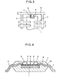
- Figs. 4 and 5 are elevational sectional views showing the structure of the pertinent part of a plastic packaged semiconductor device according to the first embodiment of the present invention.
- Fig. 4 is a drawing showing the arrangement of leads
- Fig. 5 is a drawing showing the arrangement of chip supports (only one of them is shown).
- Fig. 6 is a top view showing a plastic packaged semiconductor device according to the first embodiment in the course of its fabrication. Referring to Figs. 4 through 6, the same reference numerals as those in Figs. 1 through 3 indicate the same or corresponding members.
- the polyimide wafer coat 9 is provided on the circuit-forming surface of the semiconductor element 1.
- This semiconductor element 1 is carried by the lead frame 12 including the leads 3 and the chip supports 3.
- the leads 3 and the polyimide wafer coat 9 are just in contact and not fixed.
- the leads 3 are bent downward (toward the semiconductor element 1) outside the edge of the semiconductor 1 (at a portion indicated by reference numeral 21 in Fig. 4).
- a top surface 3a of each lead 3 (outside the bent portion 21, and disposed within the packaging material 7) and the surface of the polyimide wafer coat 9 are in substantially the same plane.
- Each chip support 10 is so disposed that its top surface 10b is substantially in the same plane as the surface of the polyimide wafer coat 9, and its end is separated by a predetermined clearance 5 from the side edge of the semiconductor element 1 (Fig. 5).
- the insulating tape 2 is adhered, bridging the top surface of the polyimide wafer coat 9 and the top surface of the chip support 10, and by means of this insulating tape 2, the polyimide wafer coat 9 and the chip support 10 are bonded and fixed.
- Fig. 6 shows a state in which the semiconductor element 1 is positioned on the lead frame 12 in this way.
- the leads 3 and the polyimide wafer coat 9 which forms the surface of the semiconductor element 1 are just in contact, and there is no material therebetween for fixing these. For this reason, the thickness of the combination of the leads 3 and the semiconductor element 1 can be reduced. The thickness of the whole device can be thereby reduced.
- the semiconductor element 1 is fixed only by means of the insulating tape 2 which is provided to bridging the polyimide wafer coat 9 and the chip support 10, the area of the tape is very small. The moisture absorption of the insulating tape 2 can be thereby reduced, and the generation of a crack during the mounting on the board can be prevented. The quality thus can be improved.
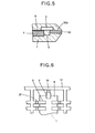
- Figs. 7 through 9 are drawings showing the structure of a plastic packaged semiconductor device according to an embodiment not of the present invention.
- Fig. 7 is a top view showing the plastic packaged semiconductor device in the course of its fabrication.
- Figs. 8 and 9 are elevational sectional views showing the structure of the pertinent part.
- Fig. 8 is a section along line A - A' in Fig. 7.
- Fig. 9 is a section alone line B - B' in Fig. 7.
- the same reference numerals as those in Figs. 1 through 6 indicate the same or corresponding members.
- the polyimide wafer coat 9 is applied to the circuit-forming surface of the semiconductor element 1.
- the chip supports 10 are attached to this polyimide wafer coat 9 by means of the insulating tape 2.
- the chip supports 10 and the leads 3 are formed in substantially the same plane.
- the chip supports 10 are bonded to the surface of the semiconductor element 1 by means of the insulating tape 2.
- gold wire platings 4 formed on the top surfaces of the leads 3 and the gold balls 5 provided on the electrodes (not shown) of the semiconductor element 1 are connected by means of the gold wires 6, whereby the leads 3 and the electrodes of the semiconductor element 1 are connected.
- the leads 3 are not bonded to the semiconductor element 1 and are kept apart. That is, the leads 3 are disposed on the semiconductor element 1 with a clearance 31 therebetween, and this clearance 31 is filled with a mold resin 7.
- the insulating tape 2 is not present in the portion below the leads 3, and the insulating tape 2 is employed only for the chip supports 10. For this reason, the amount of the insulating tape 2 used can be reduced considerably, and the moisture absorption thus can be restrained. Further, since the chip supports 10 and the leads 3 are formed in the same plane, the steps of processing the lead frame 12 such as bending can be eliminated.
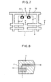
- the semiconductor element 1 to which the chip supports 10 of the lead frame 12 have been bonded by means of the insulating tape 2 is disposed within a heat block 13 as shown in Fig. 10A.
- the leads 3 and the chip supports 10 are in substantially the same plane, and the leads 3 are in the air, being apart from the semiconductor element 1 just by a thickness of the insulating tape 2 which fixes the chip supports 10 and the semiconductor element 1.
- Fig. 11 is an elevational sectional view showing the structure of the pertinent parts of a plastic packaged semiconductor device according to an embodiment not of the present invention.
- Fig. 12 shows a method of fabricating the plastic packaged semiconductor device shown in Fig. 11. Referring to Figs. 11 and 12, the same reference numerals as those in Figs. 1 through 10 indicate the same or corresponding members.
- the plastic packaged semiconductor device according to this fourth embodiment is generally the same as the plastic packaged semiconductor device in the above-mentioned third embodiment, but it is different in the following respects. That is, ends 15 of the leads 3 in the plastic packaged semiconductor device illustrated in Fig. 11 are bent upward away from the surface of the semiconductor element 1. Accordingly, when the lead clamper 14 and the heat block 13 clamp the leads 3 and the semiconductor element 1 during the fabrication process, the tips of the leads 3 do not come in direct contact with the polyimide wafer coat 9 on the semiconductor element 1, and the bottom surfaces of the ends 15 of the leads 3 which have been bent are brought into contact with the polyimide wafer coat 9. For this reason, the generation of a surface flaw on the semiconductor element 1 by the lead 3 can be prevented.
- Fig. 13 shows a method of fabricating a plastic packaged semiconductor device according to an embodiment not of the present invention.
- the same reference numerals as those in Figs. 1 through 12 indicate the same or corresponding members. It is assumed that the structure of the plastic packaged semiconductor device is the same as that of the plastic packaged semiconductor device according to the above-mentioned embodiment shown in Figs. 7 to 9,
- the gold wire platings 4 on the leads 3 and the gold balls 5 on the semiconductor element 1 are connected, using the lead clamper 16 containing an electromagnet, without bringing the leads 3 into contact with the surface of the semiconductor element 1.
- the semiconductor element 1 to which the chip supports 10 have been attached by means of the insulating tape 2 is first disposed within the heat block 13.
- the leads 3 are in the air, being apart from the semiconductor element 1 by the thickness of the insulating tape 2 which bonds the chip supports 10 to the semiconductor element 1.
- the lead clamper 16 containing the electromagnet is disposed on the top surfaces of the leads 3, and by means of a magnetic force of the lead clamper 16 containing the electromagnet, the leads 3 are fixed to the bottom surface of the lead clamper 16 containing the electromagnet, and in this state the leads 3 and the gold balls 5 on the semiconductor element 1 are subject to wire bonding by means of the gold wires 6.
- the gold balls 5 and the leads 3 By connecting the gold balls 5 and the leads 3 in this way, a surface flaw on the semiconductor element 1 and deformation of the lead 3 can be prevented.
- the fabrication method according to this embodiment may also be applied in the plastic packaged semiconductor device according to the above-mentioned embodiment shown in Figs. 11 and 12.
- Fig. 14 shows a method of fabricating a plastic packaged semiconductor device according to, an embodiment not of the present invention.
- the same reference numerals as those in Figs. 1 through 13 indicate the same or corresponding members. It is assumed that the structure of the plastic packaged semiconductor device according to this embodiment is the same as that of the plastic packaged semiconductor device according to the above-mentioned embodiment shown in Figs. 7 through 9.
- the leads 3 are brought into contact with the surface of the semiconductor element 1, using a heat block 17 containing an electromagnet.
- the semiconductor element 1 to which the chip supports 10 have been attached by means of the insulating tape 2 is first disposed within the heat block 17 containing the electromagnet.
- the heat block 17 containing the electromagnet is operated, and by means of this magnetic force, the leads 3 are pulled toward the surface of the semiconductor element 1 and brought into contact with it.
- the gold balls 5 and the leads 3 are connected by using the gold wires 6.
- the fabrication method according to this embodiment may also be applied in the plastic packaged semiconductor device according to the above-mentioned embodiment shown in Fig. 11.
- the entire semiconductor device can be made thinner.
- the generation of a crack inherent in an insulating tape for bonding can be prevented, and the quality thus can be improved.
Abstract
In a plastic packaged semiconductor device, a chip
support formed on the same lead frame as leads (3) is
disposed so as to extend over the surface of a semiconductor
element (1), the chip support is bonded and fixed to the
surface of a polyimide wafer coat (9) on the semiconductor
element (1) by means of an insulating tape, the leads (3)
are brought into contact with the polyimide wafer coat (9)
on the semiconductor element (1) without being fixed, the
leads (3) and the electrodes of the semiconductor element
(1) are connected by means of gold wires (6), and these are
packaged by a packaging material (7). Generation of crack
in the sealing material thereby prevented, and the thickness
of the plastic packaged semiconductor device is reduced.
Description
- The present invention relates to the structure of a semiconductor device, especially to the structure of a plastic packaged semiconductor device and its fabrication method.
- In recent years, in plastic packaged semiconductor devices, with an increased size of a pellet (chip), the dimension between the edge of a package and a semiconductor element tends to be increasingly smaller. This is because, although the semiconductor element has become large in size, the size of a package for housing it has been standardized and cannot be made larger. Accordingly, in order to solve such a problem, a plastic packaged semiconductor device of an LOC (Lead On Chip) structure as disclosed in Japanese Patent Kokoku Publication 6-105721 has come into use.
- The plastic packaged semiconductor device of this LOC (Lead On Chip) structure is structured such that leads are bonded to the surface of a semiconductor element via insulating tapes, gold wire platings applied to the top surfaces of the leads and gold balls on the electrodes of the semiconductor element are connected by means of gold wires, and in addition, they are sealed by a resin material.
- However, as a major problem with such conventional plastic packaged semiconductor devices, it sometimes happens, for example, that the function is impaired by a crack produced in the resin material due to the heat during the mounting on a board. If the resin becomes moist, having absorbed moisture while the semiconductor device is kept in the air, the moisture is vaporized due to the heat during the mounting on the board, and the force produced from it may bring about the crack. The insulating tape is particularly apt to absorb moisture, so that it often happens that a crack is produced from the area around the insulating tape. Further, as another problem, since there is the insulating tape, the reduction in the thickness of the semiconductor device is subject to a limitation.
- The present invention has been made in view of the above-mentioned problems. It is therefore an object of the present invention to provide a plastic packaged semiconductor device capable of preventing the generation of a crack and being made thinner, and its fabrication method.
- The present invention is characterized in that a chip support is provided besides leads, only the chip support is attached to a semiconductor element and the leads are not fixed to a semiconductor element, and the electrodes of the semiconductor element and the leads are connected.
- With this configuration, since there is no particular material between the leads and the surface of the semiconductor element for fixing them, the thickness of the combination of the leads and the semiconductor element can be reduced. The thickness of the whole device can be thereby reduced. In addition, since an insulating tape is employed solely for bonding the semiconductor element to the chip support, the area of the insulating tape to be used is very small. Generation of a crack inherent in the insulating tape can be thereby prevented, and the quality can be improved.
-
- Fig. 1 is an elevational section view showing the structure of the pertinent part of a plastic packaged semiconductor device and the arrangement of leads;
- Fig. 2 is an elevational sectional view showing the structure of the pertinent part of the plastic packaged semiconductor device of Fig. 1;
- Fig. 3 is a top view showing the plastic packaged semiconductor device of Fig. 1 in the course of its fabrication;
- Fig. 4 is an elevational sectional view showing the structure of the pertinent part of a plastic packaged semiconductor device according to a first embodiment of the present invention and the arrangement of leads;
- Fig. 5 is an elevational sectional view of the plastic packaged semiconductor device according to the first embodiment of the present invention and the arrangement of a chip support;
- Fig. 6 is a top view showing the plastic packaged semiconductor device according to the first embodiment of the present invention in the course of its fabrication;
- Fig. 7 is a top view showing a plastic packaged semiconductor device according to an embodiment not of the present invention in the course of its fabrication;
- Fig. 8 is an elevational sectional view showing the structure of the essentials of the plastic packaged semiconductor device through line A - A' in Fig. 7;
- Fig. 9 is an elevational sectional view showing the structure of the essentials of the plastic packaged semiconductor device through line B - B' in Fig. 7;
- Fig. 10A and Fig. 10B are drawings showing the process of fabrication of the plastic packaged semiconductor device according to an embodiment not of the present invention;
- Fig. 11 is an elevational sectional view showing the structure of the essentials of a plastic packaged semiconductor device according to an embodiment not of the present invention;
- Fig. 12 is a drawing showing the process of fabrication of the plastic packaged semiconductor device according to an embodiment not of the present invention;
- Fig. 13 is a drawing showing the process of fabrication of a plastic packaged semiconductor device according to an embodiment not of the present invention; and
- Fig. 14 is a drawing showing the process of fabrication of a plastic packaged semiconductor device according to an embodiment not of the present invention.
-
- Figs. 1 and 2 are elevational sectional views showing the structure of the pertinent part of a plastic packaged semiconductor device,
- Fig. 1 is a drawing showing the arrangement of leads, and Fig. 2 is a drawing showing the arrangement of chip supports (only one of them being shown). Fig. 3 is a top view showing the plastic packaged semiconductor device in the course of its fabrication.
- On the circuit-forming surface of a
semiconductor element 1, apolyimide wafer coat 9 is provided. Thissemiconductor element 1 is carried by alead frame 12 having a thickness of approximately 0.125 mm, includingleads 3 and chip supports 10. Aninsulating tape 2 having a thickness of approximately 0.15 mm is interposed between the chip supports 10 and thesemiconductor element 1, and by means of thisinsulating tape 2, the chip supports 10 and thepolyimide wafer coat 9 are bonded and fixed. The chip supports 10 are bent just by substantially the thickness (aproximately 0.15 mm) of theinsulating tape 2 outside the edge of the semiconductor element 1 (at a portion indicated byreference numeral 11 in Fig. 2). In contrast, theleads 3 and thepolyimide wafer coat 9 are just in contact with each other, and not fixed. Abottom surface 10a of the chip support 10 (outside the bent part 11) and the surface of thepolyimide wafer coat 9 are in substantially the same plane. Fig. 3 shows a state in which thesemiconductor element 1 is positioned on thelead frame 12 in this way. - Next, gold wire platings (not shown) applied to the top surfaces of the
leads 3 andgold balls 5 on thesemiconductor element 1 are connected by means ofgold wires 6. these are sealed by aresin material 7, and theleads 3 and the chip supports 10 are cut from thelead frame 12. Then, the plastic packaged semiconductor device as shown in Figs. 1 and 2 is completed. - As described above, in the structure of the plastic packaged semiconductor device
theleads 3 and thepolyimide wafer coat 9 which forms the surface of thesemiconductor element 1 are just in contact, and there is no material between them for fixing these. For this reason, the thickness of the combination of theleads 3 and thesemiconductor element 1 can be reduced. The thickness of the whole device can be thereby reduced. Thesemiconductor device 1 is fixed by means of theinsulating tape 2 alone which is adhered to the chip supports 10. Thus, the area of the tape is considerably small. The moisture absorption of theinsulating tape 2 can be thereby reduced, and the generation of a crack due to the heat which would be produced during the mounting of a board can be prevented. The quality thus can be improved. - Figs. 4 and 5 are elevational sectional views showing the structure of the pertinent part of a plastic packaged semiconductor device according to the first embodiment of the present invention. Fig. 4 is a drawing showing the arrangement of leads, and Fig. 5 is a drawing showing the arrangement of chip supports (only one of them is shown). Fig. 6 is a top view showing a plastic packaged semiconductor device according to the first embodiment in the course of its fabrication. Referring to Figs. 4 through 6, the same reference numerals as those in Figs. 1 through 3 indicate the same or corresponding members.
- On the circuit-forming surface of the
semiconductor element 1, thepolyimide wafer coat 9 is provided. Thissemiconductor element 1 is carried by thelead frame 12 including theleads 3 and the chip supports 3. Theleads 3 and thepolyimide wafer coat 9 are just in contact and not fixed. The leads 3 are bent downward (toward the semiconductor element 1) outside the edge of the semiconductor 1 (at a portion indicated byreference numeral 21 in Fig. 4). Atop surface 3a of each lead 3 (outside thebent portion 21, and disposed within the packaging material 7) and the surface of thepolyimide wafer coat 9 are in substantially the same plane. Eachchip support 10 is so disposed that itstop surface 10b is substantially in the same plane as the surface of thepolyimide wafer coat 9, and its end is separated by apredetermined clearance 5 from the side edge of the semiconductor element 1 (Fig. 5). In addition, the insulatingtape 2 is adhered, bridging the top surface of thepolyimide wafer coat 9 and the top surface of thechip support 10, and by means of this insulatingtape 2, thepolyimide wafer coat 9 and thechip support 10 are bonded and fixed. Fig. 6 shows a state in which thesemiconductor element 1 is positioned on thelead frame 12 in this way. - Next, gold wire platings applied to the top surface of the leads 3 (not shown) and the
gold balls 5 on thesemiconductor element 1 are connected by means of thegold wires 6, these are sealed by theresin material 7, and theleads 3 and the chip supports 10 are cut from thelead frame 12. Then, the plastic packaged semiconductor device as shown in Figs. 4 and 5 is completed. - As described above, in the structure of the plastic packaged semiconductor device according to the first embodiment, the
leads 3 and thepolyimide wafer coat 9 which forms the surface of thesemiconductor element 1 are just in contact, and there is no material therebetween for fixing these. For this reason, the thickness of the combination of theleads 3 and thesemiconductor element 1 can be reduced. The thickness of the whole device can be thereby reduced. In addition, since thesemiconductor element 1 is fixed only by means of the insulatingtape 2 which is provided to bridging thepolyimide wafer coat 9 and thechip support 10, the area of the tape is very small. The moisture absorption of the insulatingtape 2 can be thereby reduced, and the generation of a crack during the mounting on the board can be prevented. The quality thus can be improved. - Figs. 7 through 9 are drawings showing the structure of a plastic packaged semiconductor device according to an embodiment not of the present invention. Fig. 7 is a top view showing the plastic packaged semiconductor device in the course of its fabrication. Figs. 8 and 9 are elevational sectional views showing the structure of the pertinent part. Fig. 8 is a section along line A - A' in Fig. 7. Fig. 9 is a section alone line B - B' in Fig. 7. Referring to Figs. 7 through 9, the same reference numerals as those in Figs. 1 through 6 indicate the same or corresponding members.
- The
polyimide wafer coat 9 is applied to the circuit-forming surface of thesemiconductor element 1. The chip supports 10 are attached to thispolyimide wafer coat 9 by means of the insulatingtape 2. The chip supports 10 and theleads 3 are formed in substantially the same plane. As shown in Fig. 8, the chip supports 10 are bonded to the surface of thesemiconductor element 1 by means of the insulatingtape 2. In addition, as shown in Fig. 9,gold wire platings 4 formed on the top surfaces of theleads 3 and thegold balls 5 provided on the electrodes (not shown) of thesemiconductor element 1 are connected by means of thegold wires 6, whereby theleads 3 and the electrodes of thesemiconductor element 1 are connected. The leads 3 are not bonded to thesemiconductor element 1 and are kept apart. That is, theleads 3 are disposed on thesemiconductor element 1 with aclearance 31 therebetween, and thisclearance 31 is filled with amold resin 7. - In this way, the insulating
tape 2 is not present in the portion below theleads 3, and the insulatingtape 2 is employed only for the chip supports 10. For this reason, the amount of the insulatingtape 2 used can be reduced considerably, and the moisture absorption thus can be restrained. Further, since the chip supports 10 and theleads 3 are formed in the same plane, the steps of processing thelead frame 12 such as bending can be eliminated. - Next, a method of fabricating the plastic packaged semiconductor device shown in Figs. 7 through 9 is described with reference to Fig. 10A and Fig. 10B. First, the
semiconductor element 1 to which the chip supports 10 of thelead frame 12 have been bonded by means of the insulatingtape 2 is disposed within aheat block 13 as shown in Fig. 10A. At this time, in thelead frame 12, theleads 3 and the chip supports 10 are in substantially the same plane, and theleads 3 are in the air, being apart from thesemiconductor element 1 just by a thickness of the insulatingtape 2 which fixes the chip supports 10 and thesemiconductor element 1. - Next, as shown in Fig. 10B, by clamping the
leads 3 and thesemiconductor element 1 by means of alead clamper 14 disposed on the upper surfaces of theleads 3 and theheat block 13, theleads 3 are brought into contact with thesemiconductor element 1. Thereafter, thegold platings 4 of theleads 3 and thegold balls 5 on thesemiconductor element 1 are connected by means of wire bonding using thegold wires 6. Then, by releasing thelead clamper 14 which has been fixed, theleads 3 return to the position illustrated in Fig. 10A, and thesemiconductor element 1, leads 3,gold wires 6, and chip supports 10 are sealed by theresin material 7 in this state (refer to Figs. 8 and 9). By performing the fabrication in this way, without bending theleads 3 or the chip supports 10, a plastic packaged semiconductor device in which only the chip supports 10 have been fixed to thesemiconductor element 1 can be obtained (refer to Figs. 7 through 9). - Fig. 11 is an elevational sectional view showing the structure of the pertinent parts of a plastic packaged semiconductor device according to an embodiment not of the present invention. Fig. 12 shows a method of fabricating the plastic packaged semiconductor device shown in Fig. 11. Referring to Figs. 11 and 12, the same reference numerals as those in Figs. 1 through 10 indicate the same or corresponding members.
- The plastic packaged semiconductor device according to this fourth embodiment is generally the same as the plastic packaged semiconductor device in the above-mentioned third embodiment, but it is different in the following respects. That is, ends 15 of the
leads 3 in the plastic packaged semiconductor device illustrated in Fig. 11 are bent upward away from the surface of thesemiconductor element 1. Accordingly, when thelead clamper 14 and theheat block 13 clamp theleads 3 and thesemiconductor element 1 during the fabrication process, the tips of theleads 3 do not come in direct contact with thepolyimide wafer coat 9 on thesemiconductor element 1, and the bottom surfaces of theends 15 of theleads 3 which have been bent are brought into contact with thepolyimide wafer coat 9. For this reason, the generation of a surface flaw on thesemiconductor element 1 by thelead 3 can be prevented. - Fig. 13 shows a method of fabricating a plastic packaged semiconductor device according to an embodiment not of the present invention. Referring to Fig. 13, the same reference numerals as those in Figs. 1 through 12 indicate the same or corresponding members. It is assumed that the structure of the plastic packaged semiconductor device is the same as that of the plastic packaged semiconductor device according to the above-mentioned embodiment shown in Figs. 7 to 9,
- In the fabrication process of this plastic packaged semiconductor device according to this embodiment, the
gold wire platings 4 on theleads 3 and thegold balls 5 on thesemiconductor element 1 are connected, using thelead clamper 16 containing an electromagnet, without bringing theleads 3 into contact with the surface of thesemiconductor element 1. Referring to Fig. 13, thesemiconductor element 1 to which the chip supports 10 have been attached by means of the insulatingtape 2 is first disposed within theheat block 13. At this point in time, theleads 3 are in the air, being apart from thesemiconductor element 1 by the thickness of the insulatingtape 2 which bonds the chip supports 10 to thesemiconductor element 1. - Next, the
lead clamper 16 containing the electromagnet is disposed on the top surfaces of theleads 3, and by means of a magnetic force of thelead clamper 16 containing the electromagnet, theleads 3 are fixed to the bottom surface of thelead clamper 16 containing the electromagnet, and in this state theleads 3 and thegold balls 5 on thesemiconductor element 1 are subject to wire bonding by means of thegold wires 6. By connecting thegold balls 5 and theleads 3 in this way, a surface flaw on thesemiconductor element 1 and deformation of thelead 3 can be prevented. - The fabrication method according to this embodiment may also be applied in the plastic packaged semiconductor device according to the above-mentioned embodiment shown in Figs. 11 and 12.
- Fig. 14 shows a method of fabricating a plastic packaged semiconductor device according to, an embodiment not of the present invention. Referring to Fig. 14, the same reference numerals as those in Figs. 1 through 13 indicate the same or corresponding members. It is assumed that the structure of the plastic packaged semiconductor device according to this embodiment is the same as that of the plastic packaged semiconductor device according to the above-mentioned embodiment shown in Figs. 7 through 9.
- In the fabrication process of the plastic packaged semiconductor device according to this embodiment,the
leads 3 are brought into contact with the surface of thesemiconductor element 1, using aheat block 17 containing an electromagnet. Referring to Fig. 14, thesemiconductor element 1 to which the chip supports 10 have been attached by means of the insulatingtape 2 is first disposed within theheat block 17 containing the electromagnet. Next, theheat block 17 containing the electromagnet is operated, and by means of this magnetic force, theleads 3 are pulled toward the surface of thesemiconductor element 1 and brought into contact with it. In this state, thegold balls 5 and theleads 3 are connected by using thegold wires 6. By connecting thegold balls 5 and theleads 3 in this way, theleads 3 can be fixed stably without the use of a lead clamper. - The fabrication method according to this embodiment may also be applied in the plastic packaged semiconductor device according to the above-mentioned embodiment shown in Fig. 11.
- As described above, according to a semiconductor device and its fabrication method of the present invention, the entire semiconductor device can be made thinner. In addition, the generation of a crack inherent in an insulating tape for bonding can be prevented, and the quality thus can be improved.
Claims (3)
- A semiconductor device comprising:a semiconductor element (1) having electrodes on a surface thereof,leads connected with the electrodes;a chip support (10); an upper surface of which is disposed outside an edge of the semiconductor element to be in substantially the same plane as the surface of the semiconductor element; andan insulating tape (2) provided to bridge the chip support (10) and the semiconductor element (1) so as to attach the chip support to the semiconductor element, whereinthe leads (3) are bent toward the semiconductor element (1) outside the edge of the semiconductor element.
- The semiconductor device as set forth in claim 1, wherein the leads (3) and the electrodes are connected by wire bonding.
- The semiconductor device as set forth in claim 1 or 2, wherein a polyimide coat (9) is provided on a circuit forming surface of the semiconductor element (1).
Applications Claiming Priority (5)
| Application Number | Priority Date | Filing Date | Title |
|---|---|---|---|
| JP8114586A JPH09326463A (en) | 1996-05-09 | 1996-05-09 | Resin-sealed semiconductor device |
| JP11458696 | 1996-05-09 | ||
| JP10008397A JP3664566B2 (en) | 1997-04-17 | 1997-04-17 | Semiconductor device and manufacturing method thereof |
| JP10008397 | 1997-04-17 | ||
| EP97107671A EP0807972B1 (en) | 1996-05-09 | 1997-05-09 | Semiconductor device and method of its fabrication |
Related Parent Applications (1)
| Application Number | Title | Priority Date | Filing Date |
|---|---|---|---|
| EP97107671A Division EP0807972B1 (en) | 1996-05-09 | 1997-05-09 | Semiconductor device and method of its fabrication |
Publications (1)
| Publication Number | Publication Date |
|---|---|
| EP1381084A1 true EP1381084A1 (en) | 2004-01-14 |
Family
ID=26441172
Family Applications (2)
| Application Number | Title | Priority Date | Filing Date |
|---|---|---|---|
| EP03022551A Withdrawn EP1381084A1 (en) | 1996-05-09 | 1997-05-09 | Semiconductor device and method of its fabrication |
| EP97107671A Expired - Lifetime EP0807972B1 (en) | 1996-05-09 | 1997-05-09 | Semiconductor device and method of its fabrication |
Family Applications After (1)
| Application Number | Title | Priority Date | Filing Date |
|---|---|---|---|
| EP97107671A Expired - Lifetime EP0807972B1 (en) | 1996-05-09 | 1997-05-09 | Semiconductor device and method of its fabrication |
Country Status (4)
| Country | Link |
|---|---|
| US (2) | US5969410A (en) |
| EP (2) | EP1381084A1 (en) |
| KR (1) | KR100373891B1 (en) |
| DE (1) | DE69739619D1 (en) |
Families Citing this family (3)
| Publication number | Priority date | Publication date | Assignee | Title |
|---|---|---|---|---|
| US6975021B1 (en) * | 1999-09-03 | 2005-12-13 | Micron Technology, Inc. | Carrier for substrate film |
| KR100426330B1 (en) * | 2001-07-16 | 2004-04-08 | 삼성전자주식회사 | Ultra-Thin Semiconductor Package Device Using a Support Tape |
| KR100983882B1 (en) * | 2008-07-07 | 2010-09-27 | 주식회사 뉴인텍 | Soldering method for connecting bus bar on capacotor and products thereof |
Citations (5)
| Publication number | Priority date | Publication date | Assignee | Title |
|---|---|---|---|---|
| JPH0357255A (en) * | 1989-07-25 | 1991-03-12 | Nec Corp | Resin-sealed semiconductor device |
| US5068712A (en) * | 1988-09-20 | 1991-11-26 | Hitachi, Ltd. | Semiconductor device |
| JPH04341896A (en) * | 1991-05-20 | 1992-11-27 | Hitachi Ltd | Semiconductor device and memory card |
| US5294827A (en) * | 1992-12-14 | 1994-03-15 | Motorola, Inc. | Semiconductor device having thin package body and method for making the same |
| JPH0689947A (en) * | 1992-09-07 | 1994-03-29 | Toshiba Corp | Resin sealed type semiconductor device |
Family Cites Families (22)
| Publication number | Priority date | Publication date | Assignee | Title |
|---|---|---|---|---|
| US3887998A (en) * | 1973-11-09 | 1975-06-10 | Gen Motors Corp | Air-biased probe for semiconductor device bonding |
| US4419640A (en) * | 1979-12-17 | 1983-12-06 | Omron Tateisi Electronics Co. | Unitary contact-terminal blades integrally formed in a molded base |
| JPS60257546A (en) * | 1984-06-04 | 1985-12-19 | Mitsubishi Electric Corp | Semiconductor device and manufacture thereof |
| JPS61296730A (en) * | 1985-06-26 | 1986-12-27 | Hitachi Ltd | Wire bonder |
| JPH01134958A (en) * | 1987-11-20 | 1989-05-26 | Hitachi Ltd | Semiconductor device |
| US4935803A (en) * | 1988-09-09 | 1990-06-19 | Motorola, Inc. | Self-centering electrode for power devices |
| JP2758676B2 (en) * | 1989-12-21 | 1998-05-28 | 株式会社日立製作所 | Semiconductor device and manufacturing method thereof |
| US4989117A (en) * | 1990-02-12 | 1991-01-29 | Rogers Corporation | Molded integrated circuit package incorporating thin decoupling capacitor |
| JPH0449649A (en) * | 1990-06-18 | 1992-02-19 | Hitachi Cable Ltd | Lead frame for semiconductor device |
| US5399903A (en) * | 1990-08-15 | 1995-03-21 | Lsi Logic Corporation | Semiconductor device having an universal die size inner lead layout |
| US5146312A (en) * | 1991-02-28 | 1992-09-08 | Lim Thiam B | Insulated lead frame for semiconductor packaged devices |
| US5238174A (en) * | 1991-11-15 | 1993-08-24 | Kulicke And Soffa Investments, Inc. | Smart indexing head for universal lead frame work station |
| JPH05315526A (en) * | 1992-05-08 | 1993-11-26 | Hitachi Ltd | Semiconductor device |
| JPH0637239A (en) * | 1992-07-14 | 1994-02-10 | Hitachi Ltd | Resin-sealed semiconductor device |
| JP3128976B2 (en) * | 1992-07-31 | 2001-01-29 | ソニー株式会社 | Method for manufacturing semiconductor device |
| JP2934357B2 (en) * | 1992-10-20 | 1999-08-16 | 富士通株式会社 | Semiconductor device |
| TW270213B (en) * | 1993-12-08 | 1996-02-11 | Matsushita Electric Ind Co Ltd | |
| JPH08203945A (en) * | 1995-01-31 | 1996-08-09 | Mitsubishi Electric Corp | Wire bonding method |
| JPH08274234A (en) * | 1995-03-30 | 1996-10-18 | Hitachi Ltd | Semiconductor device, its manufacture, and semiconductor packaging module |
| US5729049A (en) * | 1996-03-19 | 1998-03-17 | Micron Technology, Inc. | Tape under frame for conventional-type IC package assembly |
| JPH09283545A (en) * | 1996-04-10 | 1997-10-31 | Oki Electric Ind Co Ltd | Resin-sealed semiconductor device and manufacture thereof |
| US6068174A (en) * | 1996-12-13 | 2000-05-30 | Micro)N Technology, Inc. | Device and method for clamping and wire-bonding the leads of a lead frame one set at a time |
-
1997
- 1997-04-29 US US08/848,286 patent/US5969410A/en not_active Expired - Lifetime
- 1997-05-08 KR KR1019970017636A patent/KR100373891B1/en not_active IP Right Cessation
- 1997-05-09 DE DE69739619T patent/DE69739619D1/en not_active Expired - Fee Related
- 1997-05-09 EP EP03022551A patent/EP1381084A1/en not_active Withdrawn
- 1997-05-09 EP EP97107671A patent/EP0807972B1/en not_active Expired - Lifetime
-
1999
- 1999-02-01 US US09/240,612 patent/US6258621B1/en not_active Expired - Fee Related
Patent Citations (5)
| Publication number | Priority date | Publication date | Assignee | Title |
|---|---|---|---|---|
| US5068712A (en) * | 1988-09-20 | 1991-11-26 | Hitachi, Ltd. | Semiconductor device |
| JPH0357255A (en) * | 1989-07-25 | 1991-03-12 | Nec Corp | Resin-sealed semiconductor device |
| JPH04341896A (en) * | 1991-05-20 | 1992-11-27 | Hitachi Ltd | Semiconductor device and memory card |
| JPH0689947A (en) * | 1992-09-07 | 1994-03-29 | Toshiba Corp | Resin sealed type semiconductor device |
| US5294827A (en) * | 1992-12-14 | 1994-03-15 | Motorola, Inc. | Semiconductor device having thin package body and method for making the same |
Non-Patent Citations (3)
| Title |
|---|
| PATENT ABSTRACTS OF JAPAN vol. 0152, no. 09 (E - 1072) 28 May 1991 (1991-05-28) * |
| PATENT ABSTRACTS OF JAPAN vol. 0171, no. 96 (M - 1397) 16 April 1993 (1993-04-16) * |
| PATENT ABSTRACTS OF JAPAN vol. 0183, no. 50 (E - 1572) 30 June 1994 (1994-06-30) * |
Also Published As
| Publication number | Publication date |
|---|---|
| KR19980079223A (en) | 1998-11-25 |
| US6258621B1 (en) | 2001-07-10 |
| EP0807972B1 (en) | 2009-10-14 |
| EP0807972A3 (en) | 2000-05-31 |
| KR100373891B1 (en) | 2003-06-18 |
| EP0807972A2 (en) | 1997-11-19 |
| US5969410A (en) | 1999-10-19 |
| DE69739619D1 (en) | 2009-11-26 |
Similar Documents
| Publication | Publication Date | Title |
|---|---|---|
| US6133068A (en) | Increasing the gap between a lead frame and a semiconductor die | |
| US5637913A (en) | Leadframe semiconductor integrated circuit device using the same and method of and process for fabricating the two | |
| US5521428A (en) | Flagless semiconductor device | |
| US5715593A (en) | Method of making plastic-packaged semiconductor integrated circuit | |
| JPH08255862A (en) | Lead frame, resin sealed semiconductor device, manufacture thereof, and molding die | |
| JPH08222681A (en) | Resin sealed semiconductor device | |
| US6127206A (en) | Semiconductor device substrate, lead frame, semiconductor device and method of making the same, circuit board, and electronic apparatus | |
| JPH0455341B2 (en) | ||
| JPH03177060A (en) | Lead frame for semiconductor device | |
| KR100366111B1 (en) | Structure of Resin Sealed Semiconductor Device | |
| JPS60167454A (en) | Semiconductor device | |
| JPH07161876A (en) | Semiconductor integrated circuit device and its manufacture, and mold used for its manufacture | |
| KR960005039B1 (en) | Semiconductor device | |
| US5969410A (en) | Semiconductor IC device having chip support element and electrodes on the same surface | |
| JPH0366152A (en) | Semiconductor integrated circuit module | |
| JPH09326463A (en) | Resin-sealed semiconductor device | |
| JP3664566B2 (en) | Semiconductor device and manufacturing method thereof | |
| JP3406147B2 (en) | Semiconductor device | |
| JPH0758273A (en) | Lead frame and semiconductor device using same | |
| JPS5930535Y2 (en) | semiconductor equipment | |
| JPH05190750A (en) | Semiconductor device | |
| JPH01206652A (en) | Semiconductor device | |
| JPH05206321A (en) | Semiconductor package | |
| JPH10107198A (en) | Ic sealing package | |
| JPH0737921A (en) | Semiconductor device |
Legal Events
| Date | Code | Title | Description |
|---|---|---|---|
| PUAI | Public reference made under article 153(3) epc to a published international application that has entered the european phase |
Free format text: ORIGINAL CODE: 0009012 |
|
| AC | Divisional application: reference to earlier application |
Ref document number: 0807972 Country of ref document: EP Kind code of ref document: P |
|
| AK | Designated contracting states |
Kind code of ref document: A1 Designated state(s): DE FR GB NL |
|
| AKX | Designation fees paid | ||
| REG | Reference to a national code |
Ref country code: DE Ref legal event code: 8566 |
|
| STAA | Information on the status of an ep patent application or granted ep patent |
Free format text: STATUS: THE APPLICATION IS DEEMED TO BE WITHDRAWN |
|
| 18D | Application deemed to be withdrawn |
Effective date: 20040715 |