EP1403921A2 - Electronic device with stacked semiconductor chips and associated manufacturing process - Google Patents
Electronic device with stacked semiconductor chips and associated manufacturing process Download PDFInfo
- Publication number
- EP1403921A2 EP1403921A2 EP03017506A EP03017506A EP1403921A2 EP 1403921 A2 EP1403921 A2 EP 1403921A2 EP 03017506 A EP03017506 A EP 03017506A EP 03017506 A EP03017506 A EP 03017506A EP 1403921 A2 EP1403921 A2 EP 1403921A2
- Authority
- EP
- European Patent Office
- Prior art keywords
- electronic component
- rewiring
- bond
- areas
- external contact
- Prior art date
- Legal status (The legal status is an assumption and is not a legal conclusion. Google has not performed a legal analysis and makes no representation as to the accuracy of the status listed.)
- Withdrawn
Links
Images


Classifications
-
- H—ELECTRICITY
- H01—ELECTRIC ELEMENTS
- H01L—SEMICONDUCTOR DEVICES NOT COVERED BY CLASS H10
- H01L25/00—Assemblies consisting of a plurality of individual semiconductor or other solid state devices ; Multistep manufacturing processes thereof
- H01L25/03—Assemblies consisting of a plurality of individual semiconductor or other solid state devices ; Multistep manufacturing processes thereof all the devices being of a type provided for in the same subgroup of groups H01L27/00 - H01L33/00, or in a single subclass of H10K, H10N, e.g. assemblies of rectifier diodes
- H01L25/04—Assemblies consisting of a plurality of individual semiconductor or other solid state devices ; Multistep manufacturing processes thereof all the devices being of a type provided for in the same subgroup of groups H01L27/00 - H01L33/00, or in a single subclass of H10K, H10N, e.g. assemblies of rectifier diodes the devices not having separate containers
- H01L25/065—Assemblies consisting of a plurality of individual semiconductor or other solid state devices ; Multistep manufacturing processes thereof all the devices being of a type provided for in the same subgroup of groups H01L27/00 - H01L33/00, or in a single subclass of H10K, H10N, e.g. assemblies of rectifier diodes the devices not having separate containers the devices being of a type provided for in group H01L27/00
- H01L25/0657—Stacked arrangements of devices
-
- H—ELECTRICITY
- H01—ELECTRIC ELEMENTS
- H01L—SEMICONDUCTOR DEVICES NOT COVERED BY CLASS H10
- H01L2224/00—Indexing scheme for arrangements for connecting or disconnecting semiconductor or solid-state bodies and methods related thereto as covered by H01L24/00
- H01L2224/01—Means for bonding being attached to, or being formed on, the surface to be connected, e.g. chip-to-package, die-attach, "first-level" interconnects; Manufacturing methods related thereto
- H01L2224/02—Bonding areas; Manufacturing methods related thereto
- H01L2224/04—Structure, shape, material or disposition of the bonding areas prior to the connecting process
- H01L2224/05—Structure, shape, material or disposition of the bonding areas prior to the connecting process of an individual bonding area
- H01L2224/0554—External layer
- H01L2224/05573—Single external layer
-
- H—ELECTRICITY
- H01—ELECTRIC ELEMENTS
- H01L—SEMICONDUCTOR DEVICES NOT COVERED BY CLASS H10
- H01L2224/00—Indexing scheme for arrangements for connecting or disconnecting semiconductor or solid-state bodies and methods related thereto as covered by H01L24/00
- H01L2224/01—Means for bonding being attached to, or being formed on, the surface to be connected, e.g. chip-to-package, die-attach, "first-level" interconnects; Manufacturing methods related thereto
- H01L2224/10—Bump connectors; Manufacturing methods related thereto
- H01L2224/15—Structure, shape, material or disposition of the bump connectors after the connecting process
- H01L2224/16—Structure, shape, material or disposition of the bump connectors after the connecting process of an individual bump connector
- H01L2224/161—Disposition
- H01L2224/16151—Disposition the bump connector connecting between a semiconductor or solid-state body and an item not being a semiconductor or solid-state body, e.g. chip-to-substrate, chip-to-passive
- H01L2224/16221—Disposition the bump connector connecting between a semiconductor or solid-state body and an item not being a semiconductor or solid-state body, e.g. chip-to-substrate, chip-to-passive the body and the item being stacked
- H01L2224/16225—Disposition the bump connector connecting between a semiconductor or solid-state body and an item not being a semiconductor or solid-state body, e.g. chip-to-substrate, chip-to-passive the body and the item being stacked the item being non-metallic, e.g. insulating substrate with or without metallisation
-
- H—ELECTRICITY
- H01—ELECTRIC ELEMENTS
- H01L—SEMICONDUCTOR DEVICES NOT COVERED BY CLASS H10
- H01L2224/00—Indexing scheme for arrangements for connecting or disconnecting semiconductor or solid-state bodies and methods related thereto as covered by H01L24/00
- H01L2224/01—Means for bonding being attached to, or being formed on, the surface to be connected, e.g. chip-to-package, die-attach, "first-level" interconnects; Manufacturing methods related thereto
- H01L2224/26—Layer connectors, e.g. plate connectors, solder or adhesive layers; Manufacturing methods related thereto
- H01L2224/31—Structure, shape, material or disposition of the layer connectors after the connecting process
- H01L2224/32—Structure, shape, material or disposition of the layer connectors after the connecting process of an individual layer connector
- H01L2224/321—Disposition
- H01L2224/32135—Disposition the layer connector connecting between different semiconductor or solid-state bodies, i.e. chip-to-chip
- H01L2224/32145—Disposition the layer connector connecting between different semiconductor or solid-state bodies, i.e. chip-to-chip the bodies being stacked
-
- H—ELECTRICITY
- H01—ELECTRIC ELEMENTS
- H01L—SEMICONDUCTOR DEVICES NOT COVERED BY CLASS H10
- H01L2224/00—Indexing scheme for arrangements for connecting or disconnecting semiconductor or solid-state bodies and methods related thereto as covered by H01L24/00
- H01L2224/01—Means for bonding being attached to, or being formed on, the surface to be connected, e.g. chip-to-package, die-attach, "first-level" interconnects; Manufacturing methods related thereto
- H01L2224/26—Layer connectors, e.g. plate connectors, solder or adhesive layers; Manufacturing methods related thereto
- H01L2224/31—Structure, shape, material or disposition of the layer connectors after the connecting process
- H01L2224/32—Structure, shape, material or disposition of the layer connectors after the connecting process of an individual layer connector
- H01L2224/321—Disposition
- H01L2224/32151—Disposition the layer connector connecting between a semiconductor or solid-state body and an item not being a semiconductor or solid-state body, e.g. chip-to-substrate, chip-to-passive
- H01L2224/32221—Disposition the layer connector connecting between a semiconductor or solid-state body and an item not being a semiconductor or solid-state body, e.g. chip-to-substrate, chip-to-passive the body and the item being stacked
- H01L2224/32225—Disposition the layer connector connecting between a semiconductor or solid-state body and an item not being a semiconductor or solid-state body, e.g. chip-to-substrate, chip-to-passive the body and the item being stacked the item being non-metallic, e.g. insulating substrate with or without metallisation
-
- H—ELECTRICITY
- H01—ELECTRIC ELEMENTS
- H01L—SEMICONDUCTOR DEVICES NOT COVERED BY CLASS H10
- H01L2224/00—Indexing scheme for arrangements for connecting or disconnecting semiconductor or solid-state bodies and methods related thereto as covered by H01L24/00
- H01L2224/01—Means for bonding being attached to, or being formed on, the surface to be connected, e.g. chip-to-package, die-attach, "first-level" interconnects; Manufacturing methods related thereto
- H01L2224/42—Wire connectors; Manufacturing methods related thereto
- H01L2224/47—Structure, shape, material or disposition of the wire connectors after the connecting process
- H01L2224/48—Structure, shape, material or disposition of the wire connectors after the connecting process of an individual wire connector
- H01L2224/4805—Shape
- H01L2224/4809—Loop shape
- H01L2224/48091—Arched
-
- H—ELECTRICITY
- H01—ELECTRIC ELEMENTS
- H01L—SEMICONDUCTOR DEVICES NOT COVERED BY CLASS H10
- H01L2224/00—Indexing scheme for arrangements for connecting or disconnecting semiconductor or solid-state bodies and methods related thereto as covered by H01L24/00
- H01L2224/01—Means for bonding being attached to, or being formed on, the surface to be connected, e.g. chip-to-package, die-attach, "first-level" interconnects; Manufacturing methods related thereto
- H01L2224/42—Wire connectors; Manufacturing methods related thereto
- H01L2224/47—Structure, shape, material or disposition of the wire connectors after the connecting process
- H01L2224/48—Structure, shape, material or disposition of the wire connectors after the connecting process of an individual wire connector
- H01L2224/481—Disposition
- H01L2224/4813—Connecting within a semiconductor or solid-state body, i.e. fly wire, bridge wire
-
- H—ELECTRICITY
- H01—ELECTRIC ELEMENTS
- H01L—SEMICONDUCTOR DEVICES NOT COVERED BY CLASS H10
- H01L2224/00—Indexing scheme for arrangements for connecting or disconnecting semiconductor or solid-state bodies and methods related thereto as covered by H01L24/00
- H01L2224/01—Means for bonding being attached to, or being formed on, the surface to be connected, e.g. chip-to-package, die-attach, "first-level" interconnects; Manufacturing methods related thereto
- H01L2224/42—Wire connectors; Manufacturing methods related thereto
- H01L2224/47—Structure, shape, material or disposition of the wire connectors after the connecting process
- H01L2224/48—Structure, shape, material or disposition of the wire connectors after the connecting process of an individual wire connector
- H01L2224/481—Disposition
- H01L2224/48151—Connecting between a semiconductor or solid-state body and an item not being a semiconductor or solid-state body, e.g. chip-to-substrate, chip-to-passive
- H01L2224/48221—Connecting between a semiconductor or solid-state body and an item not being a semiconductor or solid-state body, e.g. chip-to-substrate, chip-to-passive the body and the item being stacked
- H01L2224/48225—Connecting between a semiconductor or solid-state body and an item not being a semiconductor or solid-state body, e.g. chip-to-substrate, chip-to-passive the body and the item being stacked the item being non-metallic, e.g. insulating substrate with or without metallisation
- H01L2224/48227—Connecting between a semiconductor or solid-state body and an item not being a semiconductor or solid-state body, e.g. chip-to-substrate, chip-to-passive the body and the item being stacked the item being non-metallic, e.g. insulating substrate with or without metallisation connecting the wire to a bond pad of the item
-
- H—ELECTRICITY
- H01—ELECTRIC ELEMENTS
- H01L—SEMICONDUCTOR DEVICES NOT COVERED BY CLASS H10
- H01L2224/00—Indexing scheme for arrangements for connecting or disconnecting semiconductor or solid-state bodies and methods related thereto as covered by H01L24/00
- H01L2224/01—Means for bonding being attached to, or being formed on, the surface to be connected, e.g. chip-to-package, die-attach, "first-level" interconnects; Manufacturing methods related thereto
- H01L2224/42—Wire connectors; Manufacturing methods related thereto
- H01L2224/47—Structure, shape, material or disposition of the wire connectors after the connecting process
- H01L2224/48—Structure, shape, material or disposition of the wire connectors after the connecting process of an individual wire connector
- H01L2224/481—Disposition
- H01L2224/48151—Connecting between a semiconductor or solid-state body and an item not being a semiconductor or solid-state body, e.g. chip-to-substrate, chip-to-passive
- H01L2224/48221—Connecting between a semiconductor or solid-state body and an item not being a semiconductor or solid-state body, e.g. chip-to-substrate, chip-to-passive the body and the item being stacked
- H01L2224/48225—Connecting between a semiconductor or solid-state body and an item not being a semiconductor or solid-state body, e.g. chip-to-substrate, chip-to-passive the body and the item being stacked the item being non-metallic, e.g. insulating substrate with or without metallisation
- H01L2224/4824—Connecting between the body and an opposite side of the item with respect to the body
-
- H—ELECTRICITY
- H01—ELECTRIC ELEMENTS
- H01L—SEMICONDUCTOR DEVICES NOT COVERED BY CLASS H10
- H01L2224/00—Indexing scheme for arrangements for connecting or disconnecting semiconductor or solid-state bodies and methods related thereto as covered by H01L24/00
- H01L2224/01—Means for bonding being attached to, or being formed on, the surface to be connected, e.g. chip-to-package, die-attach, "first-level" interconnects; Manufacturing methods related thereto
- H01L2224/42—Wire connectors; Manufacturing methods related thereto
- H01L2224/47—Structure, shape, material or disposition of the wire connectors after the connecting process
- H01L2224/48—Structure, shape, material or disposition of the wire connectors after the connecting process of an individual wire connector
- H01L2224/484—Connecting portions
- H01L2224/48463—Connecting portions the connecting portion on the bonding area of the semiconductor or solid-state body being a ball bond
- H01L2224/48465—Connecting portions the connecting portion on the bonding area of the semiconductor or solid-state body being a ball bond the other connecting portion not on the bonding area being a wedge bond, i.e. ball-to-wedge, regular stitch
-
- H—ELECTRICITY
- H01—ELECTRIC ELEMENTS
- H01L—SEMICONDUCTOR DEVICES NOT COVERED BY CLASS H10
- H01L2224/00—Indexing scheme for arrangements for connecting or disconnecting semiconductor or solid-state bodies and methods related thereto as covered by H01L24/00
- H01L2224/01—Means for bonding being attached to, or being formed on, the surface to be connected, e.g. chip-to-package, die-attach, "first-level" interconnects; Manufacturing methods related thereto
- H01L2224/42—Wire connectors; Manufacturing methods related thereto
- H01L2224/47—Structure, shape, material or disposition of the wire connectors after the connecting process
- H01L2224/48—Structure, shape, material or disposition of the wire connectors after the connecting process of an individual wire connector
- H01L2224/484—Connecting portions
- H01L2224/4847—Connecting portions the connecting portion on the bonding area of the semiconductor or solid-state body being a wedge bond
- H01L2224/48471—Connecting portions the connecting portion on the bonding area of the semiconductor or solid-state body being a wedge bond the other connecting portion not on the bonding area being a ball bond, i.e. wedge-to-ball, reverse stitch
-
- H—ELECTRICITY
- H01—ELECTRIC ELEMENTS
- H01L—SEMICONDUCTOR DEVICES NOT COVERED BY CLASS H10
- H01L2224/00—Indexing scheme for arrangements for connecting or disconnecting semiconductor or solid-state bodies and methods related thereto as covered by H01L24/00
- H01L2224/73—Means for bonding being of different types provided for in two or more of groups H01L2224/10, H01L2224/18, H01L2224/26, H01L2224/34, H01L2224/42, H01L2224/50, H01L2224/63, H01L2224/71
- H01L2224/732—Location after the connecting process
- H01L2224/73201—Location after the connecting process on the same surface
- H01L2224/73203—Bump and layer connectors
- H01L2224/73204—Bump and layer connectors the bump connector being embedded into the layer connector
-
- H—ELECTRICITY
- H01—ELECTRIC ELEMENTS
- H01L—SEMICONDUCTOR DEVICES NOT COVERED BY CLASS H10
- H01L2224/00—Indexing scheme for arrangements for connecting or disconnecting semiconductor or solid-state bodies and methods related thereto as covered by H01L24/00
- H01L2224/73—Means for bonding being of different types provided for in two or more of groups H01L2224/10, H01L2224/18, H01L2224/26, H01L2224/34, H01L2224/42, H01L2224/50, H01L2224/63, H01L2224/71
- H01L2224/732—Location after the connecting process
- H01L2224/73201—Location after the connecting process on the same surface
- H01L2224/73215—Layer and wire connectors
-
- H—ELECTRICITY
- H01—ELECTRIC ELEMENTS
- H01L—SEMICONDUCTOR DEVICES NOT COVERED BY CLASS H10
- H01L2224/00—Indexing scheme for arrangements for connecting or disconnecting semiconductor or solid-state bodies and methods related thereto as covered by H01L24/00
- H01L2224/73—Means for bonding being of different types provided for in two or more of groups H01L2224/10, H01L2224/18, H01L2224/26, H01L2224/34, H01L2224/42, H01L2224/50, H01L2224/63, H01L2224/71
- H01L2224/732—Location after the connecting process
- H01L2224/73251—Location after the connecting process on different surfaces
- H01L2224/73253—Bump and layer connectors
-
- H—ELECTRICITY
- H01—ELECTRIC ELEMENTS
- H01L—SEMICONDUCTOR DEVICES NOT COVERED BY CLASS H10
- H01L2225/00—Details relating to assemblies covered by the group H01L25/00 but not provided for in its subgroups
- H01L2225/03—All the devices being of a type provided for in the same subgroup of groups H01L27/00 - H01L33/648 and H10K99/00
- H01L2225/04—All the devices being of a type provided for in the same subgroup of groups H01L27/00 - H01L33/648 and H10K99/00 the devices not having separate containers
- H01L2225/065—All the devices being of a type provided for in the same subgroup of groups H01L27/00 - H01L33/648 and H10K99/00 the devices not having separate containers the devices being of a type provided for in group H01L27/00
- H01L2225/06503—Stacked arrangements of devices
- H01L2225/0651—Wire or wire-like electrical connections from device to substrate
-
- H—ELECTRICITY
- H01—ELECTRIC ELEMENTS
- H01L—SEMICONDUCTOR DEVICES NOT COVERED BY CLASS H10
- H01L2225/00—Details relating to assemblies covered by the group H01L25/00 but not provided for in its subgroups
- H01L2225/03—All the devices being of a type provided for in the same subgroup of groups H01L27/00 - H01L33/648 and H10K99/00
- H01L2225/04—All the devices being of a type provided for in the same subgroup of groups H01L27/00 - H01L33/648 and H10K99/00 the devices not having separate containers
- H01L2225/065—All the devices being of a type provided for in the same subgroup of groups H01L27/00 - H01L33/648 and H10K99/00 the devices not having separate containers the devices being of a type provided for in group H01L27/00
- H01L2225/06503—Stacked arrangements of devices
- H01L2225/06517—Bump or bump-like direct electrical connections from device to substrate
-
- H—ELECTRICITY
- H01—ELECTRIC ELEMENTS
- H01L—SEMICONDUCTOR DEVICES NOT COVERED BY CLASS H10
- H01L2225/00—Details relating to assemblies covered by the group H01L25/00 but not provided for in its subgroups
- H01L2225/03—All the devices being of a type provided for in the same subgroup of groups H01L27/00 - H01L33/648 and H10K99/00
- H01L2225/04—All the devices being of a type provided for in the same subgroup of groups H01L27/00 - H01L33/648 and H10K99/00 the devices not having separate containers
- H01L2225/065—All the devices being of a type provided for in the same subgroup of groups H01L27/00 - H01L33/648 and H10K99/00 the devices not having separate containers the devices being of a type provided for in group H01L27/00
- H01L2225/06503—Stacked arrangements of devices
- H01L2225/06527—Special adaptation of electrical connections, e.g. rewiring, engineering changes, pressure contacts, layout
-
- H—ELECTRICITY
- H01—ELECTRIC ELEMENTS
- H01L—SEMICONDUCTOR DEVICES NOT COVERED BY CLASS H10
- H01L2225/00—Details relating to assemblies covered by the group H01L25/00 but not provided for in its subgroups
- H01L2225/03—All the devices being of a type provided for in the same subgroup of groups H01L27/00 - H01L33/648 and H10K99/00
- H01L2225/04—All the devices being of a type provided for in the same subgroup of groups H01L27/00 - H01L33/648 and H10K99/00 the devices not having separate containers
- H01L2225/065—All the devices being of a type provided for in the same subgroup of groups H01L27/00 - H01L33/648 and H10K99/00 the devices not having separate containers the devices being of a type provided for in group H01L27/00
- H01L2225/06503—Stacked arrangements of devices
- H01L2225/06555—Geometry of the stack, e.g. form of the devices, geometry to facilitate stacking
-
- H—ELECTRICITY
- H01—ELECTRIC ELEMENTS
- H01L—SEMICONDUCTOR DEVICES NOT COVERED BY CLASS H10
- H01L2225/00—Details relating to assemblies covered by the group H01L25/00 but not provided for in its subgroups
- H01L2225/03—All the devices being of a type provided for in the same subgroup of groups H01L27/00 - H01L33/648 and H10K99/00
- H01L2225/04—All the devices being of a type provided for in the same subgroup of groups H01L27/00 - H01L33/648 and H10K99/00 the devices not having separate containers
- H01L2225/065—All the devices being of a type provided for in the same subgroup of groups H01L27/00 - H01L33/648 and H10K99/00 the devices not having separate containers the devices being of a type provided for in group H01L27/00
- H01L2225/06503—Stacked arrangements of devices
- H01L2225/06582—Housing for the assembly, e.g. chip scale package [CSP]
- H01L2225/06586—Housing with external bump or bump-like connectors
-
- H—ELECTRICITY
- H01—ELECTRIC ELEMENTS
- H01L—SEMICONDUCTOR DEVICES NOT COVERED BY CLASS H10
- H01L2225/00—Details relating to assemblies covered by the group H01L25/00 but not provided for in its subgroups
- H01L2225/03—All the devices being of a type provided for in the same subgroup of groups H01L27/00 - H01L33/648 and H10K99/00
- H01L2225/04—All the devices being of a type provided for in the same subgroup of groups H01L27/00 - H01L33/648 and H10K99/00 the devices not having separate containers
- H01L2225/065—All the devices being of a type provided for in the same subgroup of groups H01L27/00 - H01L33/648 and H10K99/00 the devices not having separate containers the devices being of a type provided for in group H01L27/00
- H01L2225/06503—Stacked arrangements of devices
- H01L2225/06596—Structural arrangements for testing
-
- H—ELECTRICITY
- H01—ELECTRIC ELEMENTS
- H01L—SEMICONDUCTOR DEVICES NOT COVERED BY CLASS H10
- H01L2924/00—Indexing scheme for arrangements or methods for connecting or disconnecting semiconductor or solid-state bodies as covered by H01L24/00
- H01L2924/0001—Technical content checked by a classifier
- H01L2924/00014—Technical content checked by a classifier the subject-matter covered by the group, the symbol of which is combined with the symbol of this group, being disclosed without further technical details
-
- H—ELECTRICITY
- H01—ELECTRIC ELEMENTS
- H01L—SEMICONDUCTOR DEVICES NOT COVERED BY CLASS H10
- H01L2924/00—Indexing scheme for arrangements or methods for connecting or disconnecting semiconductor or solid-state bodies as covered by H01L24/00
- H01L2924/01—Chemical elements
- H01L2924/01068—Erbium [Er]
-
- H—ELECTRICITY
- H01—ELECTRIC ELEMENTS
- H01L—SEMICONDUCTOR DEVICES NOT COVERED BY CLASS H10
- H01L2924/00—Indexing scheme for arrangements or methods for connecting or disconnecting semiconductor or solid-state bodies as covered by H01L24/00
- H01L2924/01—Chemical elements
- H01L2924/01078—Platinum [Pt]
-
- H—ELECTRICITY
- H01—ELECTRIC ELEMENTS
- H01L—SEMICONDUCTOR DEVICES NOT COVERED BY CLASS H10
- H01L2924/00—Indexing scheme for arrangements or methods for connecting or disconnecting semiconductor or solid-state bodies as covered by H01L24/00
- H01L2924/15—Details of package parts other than the semiconductor or other solid state devices to be connected
- H01L2924/151—Die mounting substrate
- H01L2924/153—Connection portion
- H01L2924/1531—Connection portion the connection portion being formed only on the surface of the substrate opposite to the die mounting surface
- H01L2924/15311—Connection portion the connection portion being formed only on the surface of the substrate opposite to the die mounting surface being a ball array, e.g. BGA
-
- H—ELECTRICITY
- H01—ELECTRIC ELEMENTS
- H01L—SEMICONDUCTOR DEVICES NOT COVERED BY CLASS H10
- H01L2924/00—Indexing scheme for arrangements or methods for connecting or disconnecting semiconductor or solid-state bodies as covered by H01L24/00
- H01L2924/15—Details of package parts other than the semiconductor or other solid state devices to be connected
- H01L2924/181—Encapsulation
-
- H—ELECTRICITY
- H01—ELECTRIC ELEMENTS
- H01L—SEMICONDUCTOR DEVICES NOT COVERED BY CLASS H10
- H01L2924/00—Indexing scheme for arrangements or methods for connecting or disconnecting semiconductor or solid-state bodies as covered by H01L24/00
- H01L2924/19—Details of hybrid assemblies other than the semiconductor or other solid state devices to be connected
- H01L2924/191—Disposition
- H01L2924/19101—Disposition of discrete passive components
- H01L2924/19107—Disposition of discrete passive components off-chip wires
-
- H—ELECTRICITY
- H01—ELECTRIC ELEMENTS
- H01L—SEMICONDUCTOR DEVICES NOT COVERED BY CLASS H10
- H01L2924/00—Indexing scheme for arrangements or methods for connecting or disconnecting semiconductor or solid-state bodies as covered by H01L24/00
- H01L2924/30—Technical effects
- H01L2924/301—Electrical effects
- H01L2924/30107—Inductance
Definitions
- the invention relates to an electronic component with semiconductor chips in a stack and a method for producing the same.
- the invention relates to an electronic component with a stack of a logic chip in flip-chip technology and a function-tested memory chip in bond technology.
- the object of the invention is to provide a method by means of which electronic components with semiconductor chips can be produced in a stack at low cost, and the electronic components have reduced failure rates in functional tests.
- a method for producing an electronic component with semiconductor chips in a stack is created.
- a rewiring substrate is produced, the connection areas for flip-chip connections in a central area.
- the rewiring substrate has connection areas for bond connections in its edge regions.
- the rewiring substrate is thus able to electrically connect both semiconductor chips using flip-chip technology and semiconductor chips using the bonding technology of a stack to external contacts of the electronic component.
- a first electronic component in flip-chip technology designed as a semiconductor chip is next applied.
- This second electronics module is applied as the top module to the first electronics module in such a way that the passive rear sides of the first and second electronics module lie on one another.
- bond connections are made between the external contact areas of the second upper electronic component and the connection areas in the edge regions of the rewiring substrate.
- the stacked electronic components are then packaged into an electronic component by applying a plastic housing compound to the rewiring substrate.
- This method has the advantage that with the application of a rewiring structure on the active top side of the semiconductor chip of the upper electronics module, an intermediate substrate is created which gives the upper electronics module the necessary stability for handling in a test method.
- external contacts can at least temporarily act on the external contact areas of the rewiring structure be applied to test the functions of the upper electronics module independently of the stack under extreme temperature cycles. These external contacts which may be necessary for predetermined test bases can be removed again before the upper electronic component is installed in the stack in order to make the external contact surfaces available for bonding when assembling the electronic component.
- the bond connections between the edge-side external contacts of the rewiring structure of the top electronics module and the connection areas for bond connections in the edge regions of the rewiring substrate can be produced without problems and with increased reliability after the passive rear sides of the electronics modules have been brought together.
- the brittle material of the semiconductor chip of the upper component is relieved by the intermediate carrier of the rewiring structure during bonding, so that the risk of microcracks forming in the semiconductor chip during the bonding is reduced.
- the surface normals of the connection surfaces for bond connections and the surface normals of the external contact surfaces of the upper electronic module point in the same direction.
- Another possible advantage of the method is that components with a larger passive rear side than the semiconductor chips arranged below can also be used as upper electronic components to be bonded, because the stability of the upper electronic components is increased by the rewiring structure with intermediate substrate in the area of the external contact surfaces to be bonded is not bonded on the semiconductor chip, but on the intermediate substrate. This advantage is particularly noticeable when the first lower one Electronics module, a logic chip is used and a larger memory chip is used as the second upper electronics module.
- the upper electronic component Before the upper electronic component is attached to the passive rear side of the semiconductor chip of the lower electronic component, the upper electronic component can therefore be exposed to temperatures of - 50 ° C to 150 ° C if its functionality is tested.
- the module is started up electrically.
- the rewiring structure with its external contact surfaces can be adapted to the grid size of corresponding test bases.
- the above-mentioned temporary application of external contacts to the external contact areas of the rewiring structure can also provide improved contact to the test sockets. After removing the temporarily attached external contacts, the external contact areas are available again for attaching bond connections when the electronic component is being assembled.
- all signal connections of the upper electronics module can be accessed during a function test. Accordingly, a more meaningful test result is possible, especially since after the electronic component has been assembled, it is no longer possible to access all of the signal connections of the upper electronic component independently of the other electronic components in the stack. If such a function test for the upper electronic component is carried out before the electronic component is assembled, the overall yield increases and there are considerable cost advantages. This is because at least one or both of the electronic components are pre-tested, which can ensure that even electronic components with a potentially high level Failure probability such as memory chips can only be used if they have been thoroughly tested as described above. By stacking electronic components on top of each other, additional space is saved, the circuit density is increased, and costs are optimized. In addition, the electrical properties are improved since short bond connections are realized, which is associated with a reduction in parasitic inductances.
- the passive rear sides of the electronic components can be glued to one another in an advantageous manner.
- conductive adhesives can be used, for example if the back of the electronic components should have the same potential. If potential differences are provided between the backs of the electronic components, insulating adhesives can be used.
- the bond connections between the external contacts of the upper electronic component and the connection areas in the edge region of the rewiring substrate can be produced by means of thermocompression bonding.
- a bondhead is formed on one of the areas to be connected, from which the bond wire is first guided in the direction of the normal to the area before it can be bent towards the second area and is electrically connected to the second area to form a bond sheet. While the bond sheet can be attached to the second surface almost tangentially to the surface, the bond head with the bent bond wire requires a minimum height above the bonded surface.
- the bond head is first produced on the connection area for the bond connections in the edge region of the rewiring substrate, and only then is the bond bow on the external contact area of the rewiring structure of the upper electronics module is formed. This also minimizes the component height of the electronic component with semiconductor chips in a stack.
- a central bonding channel can be introduced into the rewiring structure of the upper electronic component.
- the central bond connections of this central bond channel are connected in an electrically conductive manner to the external contact areas via bond fingers and via rewiring lines.
- the external contact areas can be distributed over edge areas of the upper electronic component, whereby the bonding to the connection areas in the edge areas of the rewiring substrate is facilitated and short bond wire lengths are made possible.
- the central bond connections in the bond channel have small dimensions compared to the bond connections on the external contact surfaces, so that they are already sufficiently protected by the bond channel to such an extent that the upper electronic module with an open, unprotected bond channel can be subjected to a functional test with careful handling.
- the bond channel can advantageously be covered with a plastic protective sheath by embedding the central bond connections of the bond channel before the upper electronics module is subjected to a function test. This has the advantage that handling is facilitated both during the functional test and during subsequent assembly and damage to the central bond connections is reliably avoided.
- a circuit board metallized on both sides can be used as the rewiring substrate, the metal plating of which is structured on its top and on its underside.
- the structure of the upper side can have contact pads in a central region for flip chip connections. Connection areas for bond connections can be created in the edge regions of the upper side.
- the structured metal plating on the underside of the printed circuit board can have external contact areas which can be electrically connected to the connection areas via through contacts and via rewiring lines.
- the electronic components to be stacked have been applied to a rewiring substrate prepared in this way, the electronic components can be embedded in a filled epoxy resin using a transfer molding process.
- This packaging can be carried out simultaneously for several electronic components if the rewiring substrate used has a correspondingly large number of component positions in which electronic components are stacked and bonded. While in the transfer molding process the bond connections are heavily stressed due to the high pressure and the flow properties of the filled epoxy resin, packing the electronic components in a plastic housing by means of a dispensing process is considerably gentler.
- external contacts can be applied to the external contact areas of the rewiring substrate.
- These external contacts can have solder balls, a solder resist layer surrounding the external contact areas preventing wetting, for example, of rewiring lines by the material of the external contacts.
- the invention also relates to an electronic component with semiconductor chips in a stack, which comprises a rewiring substrate. Connection areas for flip-chip connections are provided in a central region of the rewiring substrate. In its edge areas, the rewiring substrate has connection areas for bond connections. Contact areas of a first lower electronic component designed as a semiconductor chip are connected to the connection areas in the central area of the rewiring substrate.
- a second upper electronics module has a semiconductor chip with a rewiring structure and with external contact areas. The upper electronics module is arranged on the lower electronics module in such a way that the passive rear sides of the electronics modules lie on one another. For the electrical connection of the upper electronics module to the rewiring substrate, bond connections are provided between the external contact areas of the upper electronics module and the connection areas in the edge regions of the rewiring substrate.
- the stack of at least one semiconductor chip in flip-chip technology and of an electronic component with a rewiring structure and with external contact areas is surrounded by a component housing.
- An electronic component consisting of a combination of a semiconductor chip as the first lower electronic component and a largely housed second upper electronic component has the advantage that the external contact surfaces of the upper electronic component can be used to ensure the functionality of the largely housed upper electronic component before being assembled into an electronic component to test under extreme temperature conditions so that a reliable statement can be made as to whether the stack has at least one fully functional has upper electronics module.
- Stacking reduces the space requirement and increases the circuit density. The possibility of a separate functional test of the upper electronic component results in cost optimization and reliable predictability of the final electrical properties of the electronic component.
- the lower electronics module is a logic chip and the upper electronics module is a memory chip with a rewiring structure and with external contact areas.
- Such memory chips have a relatively high failure rate in functional tests with extreme temperatures between -50 ° C and 150 ° C. This failure rate can be reduced for the electronic component with a stack of a logic chip and a memory chip if the memory chip already has a rewiring structure with external contact areas, which enables an independent, complete function test before another stack is built.
- Another advantage is that the external contact areas of the upper electronics module can be placed in the edge areas of the upper electronics module due to the wiring structure, so that extremely short bond connections from the external contact areas to the connection areas in the edge areas of the rewiring substrate are possible.
- the short bond connections ensure sufficient bond wire stability so that a highly filled epoxy resin can be used as the material for the plastic housing without taking any special precautions for protecting the bond connections.
- the rewiring structure with its intermediate substrate and the external contact areas on the upper electronic component simultaneously increases the mechanical stability of this electronic component, which increases the overall reliability of the electronic component, especially since the risk of microcracks in the semiconductor chip during bonding is reduced by the fact that it is not directly on the semiconductor chip is bonded.
- the rewiring substrate has a printed circuit board that is metallized and structured on both sides. This circuit board has through contacts as an electrical connection between the structured metal layers on the top and bottom of the circuit board.
- the underside of the circuit board has external contact areas for external contacts.
- the top of the circuit board has the connection areas for the flipchip connections in its central area and the connection areas for bond connections in its edge areas.
- the external contact areas on the underside of the printed circuit board are electrically connected to the connection areas on the top side via vias and rewiring lines.
- Such a rewiring substrate on the basis of a printed circuit board is inexpensive to produce compared to rewiring foils or rewiring substrates based on ceramics.
- An adhesive layer is arranged between the passive backs of the electronic components lying on top of one another. If the adhesive layer has a conductive adhesive, the backs of the electronic components can be at the same potential.
- An adhesive layer made of insulation adhesive can be provided, for example, between the two rear sides of the electronic components if there is a potential difference between the two electronic components on the back.
- the upper electronics module has a central bond channel with central bond connections on its active upper side. These central bond connections are connected to the external contact areas via the rewiring structure arranged on the active top side.
- This bond channel can have a protective covering for its central bond connections, as a result of which a material boundary is formed between such a protective covering and the plastic housing of the electronic component.
- Such a bond channel with central bond connections is used in particular for memory chips in order to use the relatively large active upper side of the memory chips on both sides of the bond channel for the arrangement of external contact areas.
- the bond connections between the outer contact areas and the connection areas of the outer regions of the rewiring substrate can have a bond wire which is divided into a bond head and a bond bow.
- the bonding head can be arranged on one of the connection areas of the rewiring substrate, while the bonding sheet is arranged on the corresponding external contact area of the upper electronic component.
- This embodiment of the bond connections has the advantage that a lower height is required for the bond sheet than for the bond head, so that the overall height of the electronic component can be minimized.
- an intermediate space is formed between the active top side of the semiconductor chip of the lower electronic component in the contact areas and the top side of the rewiring substrate.
- This gap is filled with an underfill that has a highly filled plastic with a fill level of 80 to 95% by weight. This high degree of filling of the underfill enables the thermal expansion behavior of the underfill to be largely adapted to the thermal expansion behavior of the semiconductor chip.
- a memory chip for example in a BOC package (board on chip package) can be used as the second upper component in an electronic component before it is glued to a logic chip using flip-chip technology with its free chip back, in its package already born or exposed to extreme temperatures and tested.
- BOC package board on chip package
- the rewiring structure with its intermediate substrate attached to the memory chip creates a very flexible housing concept with regard to design and routing or rewiring routing.
- This housing of the upper memory chip facilitates the adaptation when using memory chips from different suppliers or in the case of technology changes, since adjustments can be made via the rewiring structure without having to make changes to the rewiring substrate with the lower flip chip chip. This results in an inexpensive, flexible and adaptable structure for stacking an electronic component in flipchip technology with an electronic component in bond technology.
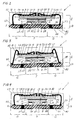
- Figure 1 shows a schematic cross section of an electronic component 1 of a first embodiment of the invention.
- the basis of this electronic component 1 is a rewiring substrate 5 with an upper side 36 and with an underside 40, which at the same time forms the underside of the electronic component 1.
- external contacts 30 are arranged in the form of contact balls, which are on external contact surfaces 27 of the rewiring substrate 5 are soldered.
- These external contact areas 27 of the rewiring substrate 5 are connected via through contacts 26 and via rewiring lines 25 of the rewiring substrate 5 to connection areas 6 and 60 on the upper side 36 of the rewiring substrate 5.
- the rewiring substrate 5 has a printed circuit board 23 as a carrier material.
- connection surfaces 6 for connecting to flip-chip contacts are arranged on the upper side 36 of the rewiring substrate 5.
- connection surfaces 60 for bond connections are arranged on the upper side 36 of the rewiring substrate 5.
- At least one logic chip 28 with its contact areas 24 is applied to the connection areas 6 of the center area 7 via the flipchip connections 8 as a first lower electronic module 9.
- the second electronic module 12 is a memory chip 39 which has a central bond channel 19 on its active upper side 32 with central bond connections 111. These central bond connections 111 of the bond channel 19 are connected via bond fingers 20 of the rewiring structure 13 to external contact areas 14 of the upper electronic component 12.
- the rewiring structure 13 has an intermediate substrate 41, on the edge regions of which the external contact areas 14 are arranged.
- the external contact areas 14 are via bond heads 33 of bond wires 18 with the connection areas 60 in the edge area 10 of the rewiring substrate 5 to form a bond sheet 34.
- a component housing 29 surrounds this stack 4 of at least one lower logic chip 28 and an upper memory chip 39 as well as the bond connections 18 between the upper memory chip 39 and the rewiring substrate 5.
- An underfill 37 which is a highly filled plastic with a degree of filling between 80 and 95% by weight. fills a gap between the active top side 35 of the logic chip 28 and the top side 36 of the rewiring substrate 5 and embeds the contact regions 24 of the logic chip 28. The high degree of filling ensures that the thermal expansion behavior of the underfill 37 is largely adapted to the thermal expansion behavior of the semiconductor material of the logic chip 28.
- a protective covering 22 covers the bonding channel 19 and protects the central bonding connections 111 of the memory chip 39. Between the protective covering 22 and the surrounding plastic housing compound 17 of the component housing 29 forms a material boundary 38.
- This electronic component 1 thus has a stack 4 made of a semiconductor chip 2 using flip-chip technology and an almost completely packaged electronic component 12.
- the functionality of this electronic component 12 has been tested under extreme temperatures between -50 and 150 ° C. before it is installed in the electronic component 1.
- This functionality test can be carried out either by connecting the external contact surfaces 14 of the upper electronic component 12 to a corresponding test socket or by temporarily applying external contacts to the external contact surfaces 14 after the test and before the installation in the electronic component 1 can be removed again.
- the underfill 37 is omitted, the gap between the active top 35 and the top 36 being filled with the plastic housing compound 17.
- FIG. 2 shows a schematic cross section of an electronic component 1 according to a second embodiment of the invention.
- Components with the same functions as in FIG. 1 are identified by the same reference symbols and are not discussed separately.
- a difference between the electronic component 1 from FIG. 1 and the electronic component 1 of the second embodiment of the invention consists in the fact that the bond wires 18 of the bond connections 11 with their bond heads 33 that stress the component height are arranged on the connection areas 60 in the edge regions 10 of the rewiring substrate 5.
- the relatively flat bond sheet 34 of such a bond connection 11 is arranged on the external contacts 14 of the upper electronic component 12. This makes it possible to limit the component height of the electronic component 1 through the protective sheath 22 of the bonding channel 19.
- the electronic component 1 thus has a lower height than the electronic component 1 from FIG. 1.
- the material boundary 38 between the plastic housing compound 17 and the plastic of the protective covering 22 of the bonding channel 19 is thus limited to the edge sides of the protective covering 22.
- FIG. 3 shows a schematic cross section of an electronic component 1 according to a third embodiment of the Invention.
- Components with the same functions as in the previous figures are identified by the same reference symbols and are not discussed separately.
- the structure of the stack of electronic components 9 and 12 is the same in the third embodiment of the invention as in the first embodiment of the invention from FIG. 1.
- the bonding channel 19 of the upper electronic component 12 is covered by the plastic housing compound 17, so that there is no material boundary 38 trained according to Figure 1.
- the method step for embedding the central bond connections 111 of the bond channel 19 in a protective sheath 22 is saved.
- the upper electronics module 12 can be tested for functionality before being installed in such an electronic component 1. It has the external contact surfaces 14 necessary for the function test.
- FIG. 4 shows a schematic cross section of an electronic component 1 of a fourth embodiment of the invention.
- Components with the same functions as in the previous figures are identified by the same reference symbols and are not discussed separately.
- This electronic component 1 of the fourth embodiment of the invention corresponds to the structure of the electronic component 1 from FIG. 2.
- the protective covering 22 of the bonding channel 19 for the upper electronic component 12 is omitted for reasons of cost savings. In this way, an electronic component 1 with a minimal component height can be implemented inexpensively.
- FIGS. 5 to 12 show schematic cross sections of intermediate products in the production of an electronic component 1 according to the first embodiment of the invention. Components with the same functions as in the previous figures are identified in FIGS. 5 to 12 with the same reference symbols and are not discussed separately.
- FIG. 5 shows a schematic cross section of a rewiring substrate 5.
- This rewiring substrate 5 is made from a printed circuit board 23 which is metallized on both sides and structured on both sides.
- the metal structure of the upper side 36 of the printed circuit board 23 is connected to the metal structure on the lower side 40 of the printed circuit board 23 via vias 26.
- the underside 40 of the printed circuit board 23 has external contact surfaces 27 which are arranged in 3 rings on the underside 40 of the printed circuit board 23.
- rewiring lines 21 are arranged, which are electrically connected to the through contacts 26.
- the rewiring lines 21 connect the through contacts 26 and thus the external contact areas 27 to connection areas 6 for the flipchip connections 8 in a central area 7 of the printed circuit board 23 and / or to connection areas 60 for the bond connections 18 in edge areas 10 of the printed circuit board 23.
- FIG. 6 shows a schematic cross section of a rewiring substrate 5 with an applied first electronic module 9.
- This electronic module 9 is connected to the connection areas 6 of the central region 7 of the rewiring substrate 5 via flip chip connections 8.
- the space between the active upper side 35 of the first lower electronic component 9 and the upper side 36 of the rewiring substrate 5 is filled with an underfill 37.
- FIG. 7 shows a schematic cross section of an electronic component 12 with an unprotected bond channel 19.
- this second electronic component 12 has a rewiring structure 13 with an intermediate substrate 41.
- this second electronic component 12 has a bond channel 19 with central bond connections 111, which are connected to external contact areas 14 of the electronic component 12 via the rewiring structure 13.
- An electronic module 12 prepared in this way is exposed to extreme temperatures between -50 and 150 ° C. before being installed in an electronic component, while its functionality is checked. This function test is also carried out without the central bond connections 111 in the bond channel 19 already being protected by a protective sheath.
- FIG. 8 shows a schematic cross section of the second electronics module 12 from FIG. 7 with a protected bonding channel 19.
- the handling of the second electronics module 12 is easier due to the protected bonding channel 19 compared to the handling of an electronics module 12 with an unprotected bonding channel 19, as shown in FIG. 7 and safer.
- the sensitive central bond connections 111 are namely embedded in the protective covering 22 and protected against mechanical damage during handling.
- FIG. 9 shows a schematic cross section through a stack 4 of a first and second electronics module 9 or 12 on the rewiring substrate 5 from FIG. 5.
- FIG. 10 shows a schematic cross section through a stack 4 from FIG. 9 after the application of bond connections 11.
- These bond connections 11 are applied to the external contact areas 14 of the rewiring structure 13 of the upper electronic module 12.
- a bond head 33 is first bonded to the external contact areas 14 and the bond wire 18 is guided downward to the connection areas 60 of the rewiring substrate 5.
- the bond wires 18 are then connected to the connection pads 60 to form a bond bow 34.
- FIG. 11 shows a schematic cross section through an electronic component 1 after the stack 4 from FIG. 10 has been packaged in a component housing 29.
- the rewiring substrate 5 with its underside 40 simultaneously forms the underside of the electronic component 1.
- a material boundary 38 is formed between the Material of the protective sheath 22 of the bond channel 19 and the plastic housing compound 17.
- FIG. 12 shows a schematic cross section through an electronic component 1 after application of external contacts 30 to the rewiring substrate 5.
- These external contacts 30 are designed here as contact balls and arranged in 3 rings.
- solderable contact balls are soldered onto the outer contact surfaces 27 on the underside 40 of the rewiring structure 5.
Abstract
Description
Elektronisches Bauteil mit Halbleiterchips in einem Stapel und Verfahren zur Herstellung desselben.Electronic component with semiconductor chips in a stack and method for producing the same.
Die Erfindung betrifft ein elektronisches Bauteil mit Halbleiterchips in einem Stapel und ein Verfahren zu Herstellung desselben. Insbesondere betrifft die Erfindung ein elektronisches Bauteil mit einem Stapel aus einem Logikchip in Flipchip-Technologie und einem funktionsgetesteten Speicherbaustein in Bondtechnologie.The invention relates to an electronic component with semiconductor chips in a stack and a method for producing the same. In particular, the invention relates to an electronic component with a stack of a logic chip in flip-chip technology and a function-tested memory chip in bond technology.
Das Bestreben immer höhere Schaltungsdichten zu erreichen, führt zu größerer Systemintegration, wobei zunehmend versucht wird, mehrere Halbleiterchips in einem Stapel anzuordnen. Dabei muß häufig ein komplettes Bauteil weggeworfen werden, nur weil der Speicherchip nicht funktioniert, obwohl der Logikchip an sich funktionsfähig ist.The desire to achieve ever higher circuit densities leads to greater system integration, with increasing efforts being made to arrange several semiconductor chips in a stack. A complete component often has to be thrown away just because the memory chip does not work, even though the logic chip itself is functional.
Aufgabe der Erfindung ist es, ein Verfahren anzugeben, mit dem elektronische Bauteile mit Halbleiterchips in einem Stapel kostengünstig hergestellt werden können, und wobei die elektronischen Bauteile in Funktionstests verminderte Ausfallraten aufweisen.The object of the invention is to provide a method by means of which electronic components with semiconductor chips can be produced in a stack at low cost, and the electronic components have reduced failure rates in functional tests.
Die Aufgabe wird mit dem Gegenstand der unabhängigen Ansprüche gelöst. Vorteilhafte Weiterbildungen der Erfindung ergeben sich aus den abhängigen Ansprüchen.The object is achieved with the subject matter of the independent claims. Advantageous developments of the invention result from the dependent claims.
Erfindungsgemäß wird ein Verfahren zur Herstellung eines elektronischen Bauteils mit Halbleiterchips in einem Stapel geschaffen. Zunächst wird dazu ein Umverdrahtungssubstrat hergestellt, das Anschlussflächen für Flipchip-Verbindungen in einem Mittenbereich aufweist. Außerdem weist das Umverdrahtungssubstrat in seinen Randbereichen Anschlussflächen für Bondverbindungen auf. Damit ist das Umverdrahtungssubstrat in der Lage, sowohl Halbleiterchips in Flipchip-Technik als auch Halbleiterchips in Bondtechnik eines Stapels mit Außenkontakten des elektronischen Bauteils elektrisch zu verbinden. Auf dieses Umverdrahtungssubstrat, das in seinem Mittenbereich Anschlussflächen für Flipchip-Verbindungen aufweist, wird als nächstes ein als Halbleiterchip ausgebildeter erster Elektronikbaustein in Flipchip-Technologie aufgebracht.According to the invention, a method for producing an electronic component with semiconductor chips in a stack is created. First of all, a rewiring substrate is produced, the connection areas for flip-chip connections in a central area. In addition, the rewiring substrate has connection areas for bond connections in its edge regions. The rewiring substrate is thus able to electrically connect both semiconductor chips using flip-chip technology and semiconductor chips using the bonding technology of a stack to external contacts of the electronic component. On this rewiring substrate, which has connection areas for flip-chip connections in its central region, a first electronic component in flip-chip technology designed as a semiconductor chip is next applied.
Parallel dazu wird wenigstens ein zweiter Elektronikbaustein hergestellt, der zusätzlich zu seinem Halbleiterchip eine Umverdrahtungsstruktur mit Außenkontaktflächen aufweist. Dieser zweite Elektronikbaustein wird als oberer Baustein auf den ersten Elektronikbaustein so aufgebracht, dass die passiven Rückseiten des ersten und des zweiten Elektronikbausteins aufeinanderliegen. Anschließend werden Bondverbindungen zwischen den Außenkontaktflächen des zweiten oberen Elektronikbausteins und den Anschlussflächen in den Randbereichen des Umverdrahtungssubstrats hergestellt. Abschließend werden dann die gestapelten Elektronikbausteine unter Aufbringen einer Kunststoffgehäusemasse auf das Umverdrahtungssubstrat zu einem elektronischen Bauteil verpackt.At the same time, at least one second electronic component is produced which, in addition to its semiconductor chip, has a rewiring structure with external contact areas. This second electronics module is applied as the top module to the first electronics module in such a way that the passive rear sides of the first and second electronics module lie on one another. Subsequently, bond connections are made between the external contact areas of the second upper electronic component and the connection areas in the edge regions of the rewiring substrate. Finally, the stacked electronic components are then packaged into an electronic component by applying a plastic housing compound to the rewiring substrate.
Dieses Verfahren hat den Vorteil, daß mit dem Aufbringen einer Umverdrahtungsstruktur auf die aktive Oberseite des Halbleiterchips des oberen Elektronikbausteins ein Zwischensubstrat geschaffen wird, das dem oberen Elektronikbaustein die nötige Stabilität für die Handhabung in einem Testverfahren verleiht. Auf die Außenkontaktflächen der Umverdrahtungsstruktur können dazu zumindest vorübergehend Außenkontakte aufgebracht werden, um die Funktionen des oberen Elektronikbausteins unabhängig von dem Stapel unter extremen Temperaturzyklen zu testen. Diese für vorgegebene Testsockel eventuell notwendigen Außenkontakte können vor dem Einbau des oberen Elektronikbausteins in den Stapel wieder entfernt werden, um die Außenkontaktflächen für ein Bonden beim Zusammenbau des elektronischen Bauteils zur Verfügung zu stellen.This method has the advantage that with the application of a rewiring structure on the active top side of the semiconductor chip of the upper electronics module, an intermediate substrate is created which gives the upper electronics module the necessary stability for handling in a test method. For this purpose, external contacts can at least temporarily act on the external contact areas of the rewiring structure be applied to test the functions of the upper electronics module independently of the stack under extreme temperature cycles. These external contacts which may be necessary for predetermined test bases can be removed again before the upper electronic component is installed in the stack in order to make the external contact surfaces available for bonding when assembling the electronic component.
Durch die erhöhte Stabilität des oberen Elektronikbausteins können die Bondverbindungen zwischen den randseitigen Außenkontakten der Umverdrahtungsstruktur des oberen Elektronikbausteins und den Anschlussflächen für Bondverbindungen in den Randbereichen des Umverdrahtungssubstrats nach dem Aufeinanderbringen der passiven Rückseiten der Elektronikbausteine unproblematisch und mit erhöhter Zuverlässigkeit hergestellt werden. Das spröde Material des Halbleiterchips des oberen Bausteins wird nämlich durch den Zwischenträger der Umverdrahtungsstruktur beim Bonden entlastet, so daß die Gefahr der Bildung von Mikrorissen in dem Halbleiterchip während des Bondens vermindert ist. Um eine Bondverbindung zu schaffen, weisen die Flächennormalen der Anschlussflächen für Bondverbindungen und die Flächennormalen der Außenkontaktflächen des oberen Elektronikbausteins in die gleiche Richtung.Due to the increased stability of the upper electronics module, the bond connections between the edge-side external contacts of the rewiring structure of the top electronics module and the connection areas for bond connections in the edge regions of the rewiring substrate can be produced without problems and with increased reliability after the passive rear sides of the electronics modules have been brought together. The brittle material of the semiconductor chip of the upper component is relieved by the intermediate carrier of the rewiring structure during bonding, so that the risk of microcracks forming in the semiconductor chip during the bonding is reduced. In order to create a bond connection, the surface normals of the connection surfaces for bond connections and the surface normals of the external contact surfaces of the upper electronic module point in the same direction.
Ein möglicher weiterer Vorteil des Verfahrens liegt darin, dass auch Bauteile mit größerer passiver Rückseite als die darunter angeordneten Halbleiterchips als zu bondende obere Elektronikbausteine eingesetzt werden können, weil die Stabilität der oberen Elektronikbausteine durch die Umverdrahtungsstruktur mit Zwischensubstrat im Bereich der zu bondenden Außenkontaktflächen erhöht ist und nicht auf dem Halbleiterchip, sondern auf dem Zwischensubstrat gebondet wird. Dieser Vorteil wirkt sich besonders aus, wenn als erster unterer Elektronikbaustein ein Logikchip eingesetzt wird und als zweiter oberer Elektronikbaustein ein flächenmäßig größerer Speicherchip verwendet wird.Another possible advantage of the method is that components with a larger passive rear side than the semiconductor chips arranged below can also be used as upper electronic components to be bonded, because the stability of the upper electronic components is increased by the rewiring structure with intermediate substrate in the area of the external contact surfaces to be bonded is not bonded on the semiconductor chip, but on the intermediate substrate. This advantage is particularly noticeable when the first lower one Electronics module, a logic chip is used and a larger memory chip is used as the second upper electronics module.
Vor einem Aufbringen des oberen Elektronikbausteins auf die passive Rückseite des Halbleiterchips des unteren Elektronikbausteins kann somit der obere Elektronikbaustein Temperaturen von - 50°C bis 150°C ausgesetzt werden, wenn seine Funktionsfähigkeit getestet wird. Dabei wird der Baustein elektrisch in Betrieb gesetzt. Dazu kann die Umverdrahtungsstruktur mit ihren Außenkontaktflächen an das Rastermaß entsprechender Testsockel angepaßt sein. Durch die oben erwähnte vorübergehende Aufbringung von Außenkontakten auf die Außenkontaktflächen der Umverdrahtungsstruktur kann darüber hinaus eine verbesserte Kontaktierung zu den Testsockeln geschaffen werden. Nach dem Entfernen der vorübergehend angebrachten Außenkontakte stehen die Außenkontaktflächen für ein Anbringen von Bondverbindungen bei dem Zusammenbau des elektronischen Bauteils wieder zur Verfügung.Before the upper electronic component is attached to the passive rear side of the semiconductor chip of the lower electronic component, the upper electronic component can therefore be exposed to temperatures of - 50 ° C to 150 ° C if its functionality is tested. The module is started up electrically. For this purpose, the rewiring structure with its external contact surfaces can be adapted to the grid size of corresponding test bases. The above-mentioned temporary application of external contacts to the external contact areas of the rewiring structure can also provide improved contact to the test sockets. After removing the temporarily attached external contacts, the external contact areas are available again for attaching bond connections when the electronic component is being assembled.
Erfindungsgemäß kann während eines Funktionstests auf sämtliche Signalanschlüsse des oberen Elektronikbausteins zugegriffen werden. Dementsprechend ist ein aussagekräftigeres Testergebnis möglich, zumal nach dem Zusammenbau des elektronischen Bauteils ein Zugriff auf alle Signalanschlüsse des oberen Elektronikbausteins unabhängig von den übrigen Elektronikbausteinen des Stapels nicht mehr möglich ist. Wird ein derartiger Funktionstest für den oberen Elektronikbaustein vor dem Zusammenbau des elektronischen Bauteils durchgeführt, so steigt die Gesamtausbeute und es ergeben sich erhebliche Kostenvorteile. Es wird nämlich mindestens einer oder beide der Elektronikbausteine vorgetestet, wodurch sichergestellt werden kann, daß auch Elektronikbausteine mit potentiell hoher Ausfallwahrscheinlichkeit wie etwa Speicherchips nur dann eingesetzt werden, wenn diese wie vorstehend beschrieben eingehend getestet wurden. Durch ein Stapeln von Elektronikbausteinen übereinander wird zusätzlich Raum eingespart, die Schaltungsdichte vergrößert, und die Kosten werden optimiert. Darüber hinaus werden die elektrischen Eigenschaften verbessert, da kurze Bondverbindungen realisiert werden, was mit einer Verminderung parasitärer Induktivitäten verbunden ist.According to the invention, all signal connections of the upper electronics module can be accessed during a function test. Accordingly, a more meaningful test result is possible, especially since after the electronic component has been assembled, it is no longer possible to access all of the signal connections of the upper electronic component independently of the other electronic components in the stack. If such a function test for the upper electronic component is carried out before the electronic component is assembled, the overall yield increases and there are considerable cost advantages. This is because at least one or both of the electronic components are pre-tested, which can ensure that even electronic components with a potentially high level Failure probability such as memory chips can only be used if they have been thoroughly tested as described above. By stacking electronic components on top of each other, additional space is saved, the circuit density is increased, and costs are optimized. In addition, the electrical properties are improved since short bond connections are realized, which is associated with a reduction in parasitic inductances.
Die passiven Rückseiten der Elektronikbausteine können in vorteilhafter Weise aufeinander geklebt werden. Dazu können Leitkleber eingesetzt werden, beispielsweise wenn die Rückseiten der Elektronikbausteine auf gleichem Potential liegen sollen. Sind Potentialdifferenzen zwischen den Rückseiten der Elektronikbausteine vorgesehen, so können isolierende Klebstoffe eingesetzt werden.The passive rear sides of the electronic components can be glued to one another in an advantageous manner. For this purpose, conductive adhesives can be used, for example if the back of the electronic components should have the same potential. If potential differences are provided between the backs of the electronic components, insulating adhesives can be used.
Die Bondverbindungen zwischen den Außenkontakten des oberen Elektronikbausteins und den Anschlussflächen im Randbereich des Umverdrahtungssubstrats können mittels Thermokompressionsbonden hergestellt werden. Dabei wird auf einer der zu verbindenden Flächen ein Bondkopf gebildet, von dem aus der Bonddraht zunächst in Richtung der Flächennormale geführt wird, bevor er zu der zweiten Fläche hin gebogen werden kann und dort unter Bildung eines Bondbogens mit der zweiten Fläche elektrisch verbunden wird. Während der Bondbogen auf der zweiten Fläche fast tangential zu der Fläche angebracht werden kann, benötigt der Bondkopf mit dem abgebogenen Bonddraht eine Mindesthöhe über der gebondeten Fläche. Deshalb ist es vorteilhaft, wenn der Bondkopf zunächst auf der Anschlussfläche für die Bondverbindungen in dem Randbereich des Umverdrahtungssubstrats hergestellt wird, und erst danach der Bondbogen auf der Außenkontaktfläche der Umverdrahtungsstruktur des oberen Elektronikbausteins gebildet wird. Dadurch wird auch die Bauteilhöhe des elektronischen Bauteils mit Halbleiterchips in einem Stapel minimiert.The bond connections between the external contacts of the upper electronic component and the connection areas in the edge region of the rewiring substrate can be produced by means of thermocompression bonding. In this case, a bondhead is formed on one of the areas to be connected, from which the bond wire is first guided in the direction of the normal to the area before it can be bent towards the second area and is electrically connected to the second area to form a bond sheet. While the bond sheet can be attached to the second surface almost tangentially to the surface, the bond head with the bent bond wire requires a minimum height above the bonded surface. It is therefore advantageous if the bond head is first produced on the connection area for the bond connections in the edge region of the rewiring substrate, and only then is the bond bow on the external contact area of the rewiring structure of the upper electronics module is formed. This also minimizes the component height of the electronic component with semiconductor chips in a stack.
In die Umverdrahtungsstruktur des oberen Elektronikbausteins kann ein zentraler Bondkanal eingebracht sein. Die zentralen Bondverbindungen dieses zentralen Bondkanals werden über Bondfinger und über Umverdrahtungsleitungen elektrisch leitend mit den Außenkontaktflächen verbunden. Die Außenkontaktflächen können auf Randbereiche des oberen Elektronikbausteins verteilt werden, wodurch das Bonden zu den Anschlussflächen in den Randbereichen des Umverdrahtungssubstrats erleichtert und kurze Bonddrähtlängen ermöglicht werden.A central bonding channel can be introduced into the rewiring structure of the upper electronic component. The central bond connections of this central bond channel are connected in an electrically conductive manner to the external contact areas via bond fingers and via rewiring lines. The external contact areas can be distributed over edge areas of the upper electronic component, whereby the bonding to the connection areas in the edge areas of the rewiring substrate is facilitated and short bond wire lengths are made possible.
Die zentralen Bondverbindungen in dem Bondkanal weisen gegenüber den Bondverbindungen auf den Außenkontaktflächen geringe Abmessungen auf, so dass sie bereits durch den Bondkanal insoweit ausreichend geschützt sind, dass der obere Elektronikbaustein mit offenem ungeschütztem Bondkanal einem Funktionstest vorsichtiger Handhabung ausgesetzt werden kann. Der Bondkanal kann jedoch in vorteilhafter Weise unter Einbetten der zentralen Bondverbindungen des Bondkanals von einer Schutzumhüllung aus Kunststoff bedeckt werden, bevor der obere Elektronikbaustein einem Funktionstest ausgesetzt wird. Dies hat den Vorteil, dass die Handhabung sowohl bei der Funktionsprüfung als auch bei dem späteren Zusammenbau erleichtert wird und eine Beschädigung der zentralen Bondverbindungen zuverlässig vermieden wird.The central bond connections in the bond channel have small dimensions compared to the bond connections on the external contact surfaces, so that they are already sufficiently protected by the bond channel to such an extent that the upper electronic module with an open, unprotected bond channel can be subjected to a functional test with careful handling. However, the bond channel can advantageously be covered with a plastic protective sheath by embedding the central bond connections of the bond channel before the upper electronics module is subjected to a function test. This has the advantage that handling is facilitated both during the functional test and during subsequent assembly and damage to the central bond connections is reliably avoided.
Als Umverdrahtungssubstrat kann eine beidseitig metallisierte Leiterplatte eingesetzt werden, deren Metallplattierungen auf ihrer Oberseite und auf ihrer Unterseite strukturiert werden. Die Struktur der Oberseite kann in einem Mittenbereich Kontaktanschlußflächen für Flipchip-Verbindungen aufweisen. In den Randbereichen der Oberseite können Anschlussflächen für Bondverbindungen geschaffen werden. Die strukturierte Metallplattierung auf der Unterseite der Leiterplatte kann Außenkontaktflächen aufweisen, die mit den Anschlussflächen über Durchkontakte und über Umverdrahtungsleitungen elektrisch verbunden werden können. Ein derartiges Umverdrahtungssubstrat auf der Basis einer beidseitig metallisierten und strukturierten Leiterplatte kann kostengünstig hergestellt werden und hat gegenüber Umverdrahtungssubstraten auf Keramikbasis einen erheblichen Preisvorteil.A circuit board metallized on both sides can be used as the rewiring substrate, the metal plating of which is structured on its top and on its underside. The structure of the upper side can have contact pads in a central region for flip chip connections. Connection areas for bond connections can be created in the edge regions of the upper side. The structured metal plating on the underside of the printed circuit board can have external contact areas which can be electrically connected to the connection areas via through contacts and via rewiring lines. Such a rewiring substrate based on a metallized and structured printed circuit board on both sides can be produced inexpensively and has a considerable price advantage over rewiring substrates based on ceramics.
Nach dem Aufbringen der zu stapelnden Elektronikbausteine auf ein derartig präpariertes Umverdrahtungssubstrat können die Elektronikbausteine mittels einem Transfermoldverfahren in ein gefülltes Epoxidharz eingebettet werden. Dieses Verpacken kann gleichzeitig für mehrere elektronische Bauteile durchgeführt werden, wenn das verwendete Umverdrahtungssubstrat entsprechend viele Bauteilpositionen aufweist, in denen Elektronikbausteine gestapelt und gebondet sind. Während beim Transfermoldverfahren die Bondverbindungen aufgrund des hohen Druckes und der Fließeigenschaften des gefüllten Epoxidharzes stark belastet werden, ist ein Verpacken der Elektronikbausteine in ein Kunststoffgehäuse mittels Dispensverfahren wesentlichen schonender.After the electronic components to be stacked have been applied to a rewiring substrate prepared in this way, the electronic components can be embedded in a filled epoxy resin using a transfer molding process. This packaging can be carried out simultaneously for several electronic components if the rewiring substrate used has a correspondingly large number of component positions in which electronic components are stacked and bonded. While in the transfer molding process the bond connections are heavily stressed due to the high pressure and the flow properties of the filled epoxy resin, packing the electronic components in a plastic housing by means of a dispensing process is considerably gentler.
Abschließend können auf die Außenkontaktflächen des Umverdrahtungssubstrats Außenkontakte aufgebracht werden. Diese Außenkontakte können Lötbälle aufweisen, wobei eine die Außenkontaktflächen umgebende Lötstopplackschicht ein Benetzen beispielsweise von Umverdrahtungsleitungen durch das Material der Außenkontakte verhindert.Finally, external contacts can be applied to the external contact areas of the rewiring substrate. These external contacts can have solder balls, a solder resist layer surrounding the external contact areas preventing wetting, for example, of rewiring lines by the material of the external contacts.
Die Erfindung betrifft auch ein elektronisches Bauteil mit Halbleiterchips in einem Stapel, das ein Umverdrahtungssubstrat umfaßt. In einem Mittenbereich des Umverdrahtungssubstrats sind Anschlussflächen für Flipchip-Verbindungen vorgesehen. In seinen Randbereichen weist das Umverdrahtungssubstrat Anschlussflächen für Bondverbindungen auf. Kontaktbereiche eines als Halbleiterchip ausgebildeten ersten unteren Elektronikbausteins sind mit den Anschlussflächen in dem Mittenbereich des Umverdrahtungssubstrats verbunden. Ein zweiter oberer Elektronikbaustein weist einen Halbleiterchip mit einer Umverdrahtungsstruktur und mit Außenkontaktflächen auf. Der obere Elektronikbausteine ist derart auf dem unteren Elektronikbaustein angeordnet, dass die passiven Rückseiten der Elektronikbausteine aufeinanderliegen. Zur elektrischen Verbindung des oberen Elektronikbausteins mit dem Umverdrahtungssubstrat sind zwischen den Außenkontaktflächen des oberen Elektronikbausteins und den Anschlussflächen in den Randbereichen des Umverdrahtungssubstrats Bondverbindungen vorgesehen.The invention also relates to an electronic component with semiconductor chips in a stack, which comprises a rewiring substrate. Connection areas for flip-chip connections are provided in a central region of the rewiring substrate. In its edge areas, the rewiring substrate has connection areas for bond connections. Contact areas of a first lower electronic component designed as a semiconductor chip are connected to the connection areas in the central area of the rewiring substrate. A second upper electronics module has a semiconductor chip with a rewiring structure and with external contact areas. The upper electronics module is arranged on the lower electronics module in such a way that the passive rear sides of the electronics modules lie on one another. For the electrical connection of the upper electronics module to the rewiring substrate, bond connections are provided between the external contact areas of the upper electronics module and the connection areas in the edge regions of the rewiring substrate.
Der Stapel aus mindestens einem Halbleiterchip in Flipchip-Technologie und aus einem Elektronikbaustein mit einer Umverdrahtungsstruktur und mit Außenkontaktflächen ist von einem Bauteilgehäuse umgeben. Ein elektronisches Bauteil aus einer Kombination aus einem Halbleiterchip als ersten unteren Elektronikbaustein und aus einem weitgehend gehäusten zweiten oberen Elektronikbaustein hat den Vorteil, dass die Außenkontaktflächen des oberen Elektronikbausteins eingesetzt werden können, um vor einem Zusammenbau zu einem elektronischen Bauteil die Funktionsfähigkeit des weitgehend gehäusten oberen Elektronikbausteins unter extremen Temperaturbedingungen zu testen, so daß eine zuverlässige Aussage darüber getätigt werden kann, ob der Stapel wenigstens einen vollständig funktionsfähigen oberen Elektronikbaustein aufweist. Durch das Stapeln wird der Platzbedarf vermindert und die Schaltungsdichte erhöht. Durch die Möglichkeit einer separaten Funktionsprüfung des oberen Elektronikbausteins ergibt sich eine Kostenoptimierung und eine zuverlässige Prognostizierbarkeit der endgültigen elektrischen Eigenschaften des elektronischen Bauteils.The stack of at least one semiconductor chip in flip-chip technology and of an electronic component with a rewiring structure and with external contact areas is surrounded by a component housing. An electronic component consisting of a combination of a semiconductor chip as the first lower electronic component and a largely housed second upper electronic component has the advantage that the external contact surfaces of the upper electronic component can be used to ensure the functionality of the largely housed upper electronic component before being assembled into an electronic component to test under extreme temperature conditions so that a reliable statement can be made as to whether the stack has at least one fully functional has upper electronics module. Stacking reduces the space requirement and increases the circuit density. The possibility of a separate functional test of the upper electronic component results in cost optimization and reliable predictability of the final electrical properties of the electronic component.
Diese Vorteile wirken sich besonders aus, wenn der untere Elektronikbaustein ein Logikchip und der obere Elektronikbaustein ein Speicherchip mit Umverdrahtungsstruktur und mit Außenkontaktflächen ist. Derartige Speicherchips weisen eine relativ hohe Ausfallrate bei Funktionstests mit extremen Temperaturen zwischen -50°C und 150°C auf. Diese Ausfallrate kann für das elektronische Bauteil mit einem Stapel aus einem Logikchip und aus einem Speicherchip vermindert werden, wenn der Speicherchip bereits eine Umverdrahtungsstruktur mit Außenkontakflächen aufweist, durch die ein unabhängiger vollständiger Funktionstest vor einem weiteren Stapelbau möglich wird.These advantages have a particular effect if the lower electronics module is a logic chip and the upper electronics module is a memory chip with a rewiring structure and with external contact areas. Such memory chips have a relatively high failure rate in functional tests with extreme temperatures between -50 ° C and 150 ° C. This failure rate can be reduced for the electronic component with a stack of a logic chip and a memory chip if the memory chip already has a rewiring structure with external contact areas, which enables an independent, complete function test before another stack is built.
Ein weiterer Vorteil besteht darin, dass die Außenkontaktflächen des oberen Elektronikbausteins auf Grund der Verdrahtungstruktur in die Randbereiche des oberen Elektronikbausteins gelegt werden können, sodass äußerst kurze Bondverbindungen von den Außerkontaktflächen zu den Anschlussflächen in den Randbereichen des Umverdrahtungssubstrats möglich werden. Durch die kurzen Bondverbindungen wird eine ausreichende Bonddrahtstabilität erreicht, sodass als Material für das Kunststoffgehäuse ein hochgefülltes Epoxidharz eingesetzt werden kann, ohne besondere Vorkehrungen für den Schutz der Bondverbindungen zu treffen.Another advantage is that the external contact areas of the upper electronics module can be placed in the edge areas of the upper electronics module due to the wiring structure, so that extremely short bond connections from the external contact areas to the connection areas in the edge areas of the rewiring substrate are possible. The short bond connections ensure sufficient bond wire stability so that a highly filled epoxy resin can be used as the material for the plastic housing without taking any special precautions for protecting the bond connections.
Die Umverdrahtungsstruktur mit ihrem Zwischensubstrat und den Außenkontaktflächen auf dem oberen Elektronikbaustein vergrößert gleichzeitig die mechanische Stabilität dieses Elektronikbausteins, wodurch die gesamte Zuverlässigkeit des elektronischen Bauteils erhöht ist, zumal die Gefahr von Mikrorissbildungen in dem Halbleiterchip beim Bonden dadurch vermindert wird, daß nicht unmittelbar auf dem Halbleiterchip gebondet wird.The rewiring structure with its intermediate substrate and the external contact areas on the upper electronic component simultaneously increases the mechanical stability of this electronic component, which increases the overall reliability of the electronic component, especially since the risk of microcracks in the semiconductor chip during bonding is reduced by the fact that it is not directly on the semiconductor chip is bonded.
Das Umverdrahtungssubstrat weist eine beidseitig metallisierte und strukturierte Leiterplatte auf. Diese Leiterplatte verfügt über Durchkontakte als elektrische Verbindung zwischen den strukturierten Metallschichten auf der Ober- und auf der Unterseite der Leiterplatte. Die Unterseite der Leiterplatte weist Außenkontaktflächen für Außenkontakte auf. Die Oberseite der Leiterplatte weist in ihrem Mittenbereich die Anschlussflächen für die Flipchip-Verbindungen und in ihren Randbereichen die Anschlussflächen für Bondverbindungen auf. Die Außenkontaktflächen auf der Unterseite der Leiterplatte sind über Durchkontakte und über Umverdrahtungsleitungen mit den Anschlussflächen auf der Oberseite elektrisch verbunden. Ein derartiges Umverdrahtungssubstrat auf der Basis einer Leiterplatte ist kostengünstig herstellbar verglichen mit Umverdrahtungsfolien oder Umverdrahtungssubstraten auf der Basis von Keramiken.The rewiring substrate has a printed circuit board that is metallized and structured on both sides. This circuit board has through contacts as an electrical connection between the structured metal layers on the top and bottom of the circuit board. The underside of the circuit board has external contact areas for external contacts. The top of the circuit board has the connection areas for the flipchip connections in its central area and the connection areas for bond connections in its edge areas. The external contact areas on the underside of the printed circuit board are electrically connected to the connection areas on the top side via vias and rewiring lines. Such a rewiring substrate on the basis of a printed circuit board is inexpensive to produce compared to rewiring foils or rewiring substrates based on ceramics.
Zwischen den aufeinanderliegenden passiven Rückseiten der Elektronikbausteine ist eine Klebstoffschicht angeordnet. Wenn die Klebstoffschicht einen Leitkleber aufweist, können die Rückseiten der Elektronikbausteine auf gleichem Potential liegen. Eine Klebstoffschicht aus Isolationsklebstoff kann beispielsweise dann zwischen beiden Rückseiten der Elektronikbausteine vorgesehen werden, wenn eine Potentialdifferenz zwischen beiden Elektronikbausteinen an den Rückseiten gewünscht ist.An adhesive layer is arranged between the passive backs of the electronic components lying on top of one another. If the adhesive layer has a conductive adhesive, the backs of the electronic components can be at the same potential. An adhesive layer made of insulation adhesive can be provided, for example, between the two rear sides of the electronic components if there is a potential difference between the two electronic components on the back.
Der obere Elektronikbaustein weist auf seiner aktiven Oberseite einen zentralen Bondkanal mit zentralen Bondverbindungen auf. Diese zentralen Bondverbindungen sind über die auf der aktiven Oberseite angeordnete Umverdrahtungsstruktur mit den Außenkontaktflächen verbunden. Dieser Bondkanal kann eine Schutzumhüllung für seine zentralen Bondverbindungen aufweisen, wodurch sich eine Materialgrenze zwischen einer derartigen Schutzumhüllung und dem Kunststoffgehäuse des elektronischen Bauteils ausbildet. Ein derartiger Bondkanal mit zentralen Bondverbindungen wird insbesondere für Speicherchips eingesetzt, um die relativ große aktive Oberseite der Speicherchips zu beiden Seiten des Bondkanals für das Anordnen von Außenkontaktflächen zu nutzen.The upper electronics module has a central bond channel with central bond connections on its active upper side. These central bond connections are connected to the external contact areas via the rewiring structure arranged on the active top side. This bond channel can have a protective covering for its central bond connections, as a result of which a material boundary is formed between such a protective covering and the plastic housing of the electronic component. Such a bond channel with central bond connections is used in particular for memory chips in order to use the relatively large active upper side of the memory chips on both sides of the bond channel for the arrangement of external contact areas.
Die Bondverbindungen zwischen den Außenkontaktflächen und den Anschlussflächen der Außenbereiche des Umverdrahtungssubstrats können einen Bonddraht aufweisen, der sich in einen Bondkopf und in einen Bondbogen gliedert. Der Bondkopf kann auf einer der Anschlussflächen des Umverdrahtungssubstrats angeordnet sein, während der Bondbogen auf der entsprechenden Außenkontaktfläche des oberen Elektronikbausteins angeordnet ist. Diese Ausführung der Bondverbindungen hat den Vorteil, dass für den Bondbogen eine geringere Höhe beansprucht wird, als für den Bondkopf, so daß die Gesamthöhe des elektronischen Bauteils minimiert werden kann.The bond connections between the outer contact areas and the connection areas of the outer regions of the rewiring substrate can have a bond wire which is divided into a bond head and a bond bow. The bonding head can be arranged on one of the connection areas of the rewiring substrate, while the bonding sheet is arranged on the corresponding external contact area of the upper electronic component. This embodiment of the bond connections has the advantage that a lower height is required for the bond sheet than for the bond head, so that the overall height of the electronic component can be minimized.
Weiterhin ist vorgesehen, dass zwischen der aktiven Oberseite des Halbleiterchips des unteren Elektronikbausteins bei den Kontaktbereichen und der Oberseite des Umverdrahtungssubstrats ein Zwischenraum ausgebildet ist. Dieser Zwischenraum ist mit einem Unterfüllstoff aufgefüllt, der einen hochgefüllten Kunststoff mit einem Füllgrad von 80 bis 95 Gew.% aufweist. Dieser hohe Füllgrad des Unterfüllstoffes ermöglicht eine weitgehende Anpassung des thermischen Ausdehnungsverhaltens des Unterfüllstoffes an das thermische Ausdehnungsverhalten des Halbleiterchips.Furthermore, it is provided that an intermediate space is formed between the active top side of the semiconductor chip of the lower electronic component in the contact areas and the top side of the rewiring substrate. This gap is filled with an underfill that has a highly filled plastic with a fill level of 80 to 95% by weight. This high degree of filling of the underfill enables the thermal expansion behavior of the underfill to be largely adapted to the thermal expansion behavior of the semiconductor chip.
Zusammenfassend ist festzustellen, dass ein Speicherchip beispielsweise in einem BOC-Gehäuse (board on chip package) als zweiter oberer Baustein in einem elektronischen Bauteil eingesetzt werden kann, bevor er mit seiner freibleibenden Chiprückseite auf einen Logikchip in Flipchip-Technik geklebt wird, in seinem Gehäuse bereits geburnt bzw. extremen Temperaturen ausgesetzt und getestet werden kann. Durch Optimieren des Bondprozesses beim Verbinden des oberen Speicherchips mit dem Umverdrahtungssubstrat kann außerdem eine raumsparende Stapelung eines Speicherchips auf einem Logikchip erreicht werden.In summary, it can be stated that a memory chip, for example in a BOC package (board on chip package), can be used as the second upper component in an electronic component before it is glued to a logic chip using flip-chip technology with its free chip back, in its package already born or exposed to extreme temperatures and tested. By optimizing the bonding process when connecting the upper memory chip to the rewiring substrate, space-saving stacking of a memory chip on a logic chip can also be achieved.
Durch die auf dem Speicherchip angebrachte Umverdrahtungsstruktur mit ihrem Zwischensubstrat entsteht bezüglich Design und Routing bzw. Umverdrahtungsführung ein sehr flexibles Gehäusekonzept. Dieses Gehäuse des oberen Speicherchips erleichtert die Anpassung beim Verwenden von Speicherbausteinen verschiedener Zulieferer oder bei Technologieänderungen, da über die Umverdrahtungsstruktur Anpassungen vorgenommen werden können, ohne dass Veränderungen des Umverdrahtungssubstrats mit dem unteren Flipchip-Baustein vorgenommen werden müssen. Somit ergibt sich ein kostengünstiger, flexibler und anpassungfähiger Aufbau zum Stapeln eines Elektronikbausteins in Flipchip-Technologie mit einem Elektronikbaustein in Bond-Technologie.The rewiring structure with its intermediate substrate attached to the memory chip creates a very flexible housing concept with regard to design and routing or rewiring routing. This housing of the upper memory chip facilitates the adaptation when using memory chips from different suppliers or in the case of technology changes, since adjustments can be made via the rewiring structure without having to make changes to the rewiring substrate with the lower flip chip chip. This results in an inexpensive, flexible and adaptable structure for stacking an electronic component in flipchip technology with an electronic component in bond technology.
Die Erfindung wird nun anhand der beigefügten Figuren näher erläutert.
- Figur 1
- zeigt einen schematischen Querschnitt eines elektronischen Bauteils gemäß einer ersten Ausführungsform der Erfindung,
Figur 2- zeigt einen schematischen Querschnitt eines elektronischen Bauteils einer zweiten Ausführungsform der Erfindung,
Figur 3- zeigt einen schematischen Querschnitt eines elektronischen Bauteils einer dritten Ausführungsform der Erfindung,
Figur 4- zeigt einen schematischen Querschnitt eines elektronischen Bauteils einer vierten Ausführungsform der Erfindung,
Figuren 5bis 11- zeigen schematische Querschnitte von Zwischenprodukten bei der Herstellung des elektronischen Bauteils gemäß der ersten Ausführungsform der Erfindung,
Figur 5- zeigt einen schematischen Querschnitt eines Umverdrahtungssubstrats,
Figur 6- zeigt einen schematischen Querschnitt eines Umverdrahtungssubstrats mit einem aufgebrachten ersten Elektronikbaustein,
Figur 7- zeigt einen schematischen Querschnitt eines zweiten Elektronikbausteins mit einem ungeschützten Bondkanal,
Figur 8- zeigt einen schematischen Querschnitt des zweiten Elektronikbausteins aus Fig.7 mit einem geschützten Bondkanal,
Figur 9- zeigt einen schematischen Querschnitt durch einen Stapel mit dem erstem Elektronikbaustein und mit dem zweitem Elektronikbaustein auf dem
Umverdrahtungssubstrat aus Figur 5, Figur 10- zeigt einen schematischen Querschnitt durch einen
Stapel aus Figur 9 nach Aufbringen von Bondverbindungen, Figur 11- zeigt einen schematischen Querschnitt durch ein elektronisches Bauteil nach Verpacken des Stapels aus Figur 10 in einem Bauteilgehäuse,
Figur 12- zeigt einen schematischen Querschnitt durch ein elektronisches Bauteil nach Aufbringen von Außenkontakten auf das Umverdrahtungssubstrat des elektronischen Bauteils.
- Figure 1
- shows a schematic cross section of an electronic component according to a first embodiment of the invention,
- Figure 2
- shows a schematic cross section of an electronic component of a second embodiment of the invention,
- Figure 3
- shows a schematic cross section of an electronic component of a third embodiment of the invention,
- Figure 4
- shows a schematic cross section of an electronic component of a fourth embodiment of the invention,
- Figures 5 to 11
- show schematic cross sections of intermediate products in the production of the electronic component according to the first embodiment of the invention,
- Figure 5
- shows a schematic cross section of a rewiring substrate,
- Figure 6
- shows a schematic cross section of a rewiring substrate with an applied first electronic module,
- Figure 7
- shows a schematic cross section of a second electronic module with an unprotected bond channel,
- Figure 8
- shows a schematic cross section of the second electronic module from FIG. 7 with a protected bond channel,
- Figure 9
- shows a schematic cross section through a stack with the first electronics module and with the second electronics module on the rewiring substrate from FIG. 5,
- Figure 10
- shows a schematic cross section through a stack from FIG. 9 after bonding connections have been applied,
- Figure 11
- 10 shows a schematic cross section through an electronic component after packaging the stack from FIG. 10 in a component housing,
- Figure 12
- shows a schematic cross section through an electronic component after applying external contacts to the rewiring substrate of the electronic component.
Figur 1 zeigt einen schematischen Querschnitt eines elektronischen Bauteils 1 einer ersten Ausführungsform der Erfindung. Die Basis dieses elektronischen Bauteils 1 bildet ein Umverdrahtungssubstrat 5 mit einer Oberseite 36 und mit einer Unterseite 40, die gleichzeitig die Unterseite des elektronischen Bauteils 1 bildet. Auf der Unterseite 40 sind Außenkontakte 30 in Form von Kontaktbällen angeordnet, die auf Außenkontaktflächen 27 des Umverdrahtungssubstrats 5 gelötet sind. Diese Außenkontaktflächen 27 des Umverdrahtungssubstrats 5 sind über Durchkontakte 26 und über Umverdrahtungsleitungen 25 des Umverdrahtungssubstrats 5 mit Anschlussflächen 6 und 60 auf der Oberseite 36 des Umverdrahtungssubstrats 5 verbunden. Das Umverdrahtungssubstrat 5 weist in dieser ersten Ausführungsform der Erfindung eine Leiterplatte 23 als Trägermaterial auf.Figure 1 shows a schematic cross section of an electronic component 1 of a first embodiment of the invention. The basis of this electronic component 1 is a
In einem Mittenbereich 7 sind auf der Oberseite 36 des Umverdrahtungssubstrats 5 Anschlussflächen 6 zum Verbinden mit Flipchip-Kontakten angeordnet. In den Randbereichen 10 sind auf der Oberseite 36 des Umverdrahtungssubstrats 5 Anschlussflächen 60 für Bondverbindungen angeordnet. Auf den Anschlussflächen 6 des Mittenbereichs 7 ist wenigstens ein Logikchip 28 mit seinen Kontaktbereichen 24 über die Flipchip-Verbindungen 8 als ein erster unterer Elektronikbaustein 9 aufgebracht. Auf der passiven Rückseite 15 dieses ersten Elektronikbausteins 9 ist eine Klebeschicht 31 angeordnet, mit der ein zweiter oberer Elektronikbaustein 12 auf dem ersten unteren Elektronikbaustein 9 angeordnet ist.In a
Bei dem zweiten Elektronikbaustein 12 handelt es sich um einen Speicherchip 39, der einen zentralen Bondkanal 19 auf seiner aktiven Oberseite 32 mit zentralen Bondverbindungen 111 aufweist. Diese zentralen Bondverbindungen 111 des Bondkanals 19 sind über Bondfinger 20 der Umverdrahtungsstruktur 13 mit Außenkontaktflächen 14 des oberen Elektronikbausteins 12 verbunden. Die Umverdrahtungsstruktur 13 weist ein Zwischensubstrat 41 auf, auf dessen Randbereichen die Außenkontaktflächen 14 angeordnet sind. Die Außenkontaktflächen 14 sind über Bondköpfe 33 von Bonddrähten 18 mit den Anschlussflächen 60 in dem Randbereich 10 des Umverdrahtungssubstrats 5 unter Ausbildung eines Bondbogens 34 verbunden.The second
Ein Bauteilgehäuse 29 umgibt diesen Stapel 4 aus mindestens einem unteren Logikchip 28 und einem oberen Speicherchips 39 sowie die Bondverbindungen 18 zwischen dem oberen Speicherchip 39 und dem Umverdrahtungssubstrat 5. Ein Unterfüllstoff 37, der einen hochgefüllten Kunststoff mit einem Füllgrad zwischen 80 und 95 Gew.% aufweist, füllt einen Zwischenraum zwischen der aktiven Oberseite 35 des Logikchips 28 und der Oberseite 36 des Umverdrahtungssubstrats 5 und bettet die Kontaktbereiche 24 des Logikchips 28 ein. Der hohe Füllgrad sorgt für eine weitgehende Anpassung des thermischen Ausdehnungsverhaltens des Unterfüllstoffes 37 an das thermische Ausdehnungsverhalten des Halbleitermaterials des Logikchips 28. Eine Schutzumhüllung 22 deckt den Bondkanal 19 ab und schützt die zentralen Bondverbindungen 111 des Speicherchips 39. Zwischen der Schutzumhüllung 22 und der umgebenden Kunststoffgehäusemasse 17 des Bauteilgehäuses 29 bildet sich eine Materialgrenze 38 aus.A
Dieses elektronische Bauteil 1 weist somit einen Stapel 4 aus einem Halbleiterchip 2 in Flipchip-Technologie und aus einem nahezu vollständig gehäusten Elektronikbaustein 12 auf. Die Funktionsfähigkeit dieses Elektronikbausteins 12 ist vor seinem Einbau in das elektronische Bauteil 1 unter extremen Temperaturen zwischen -50 und 150 °C getestet worden. Dieser Funktionsfähigkeitstest kann durchgeführt werden, indem entweder die Außenkontaktflächen 14 des oberen Elektronikbausteins 12 mit einem entsprechenden Prüfsockel verbunden werden oder indem Außenkontakte vorübergehend auf die Außenkontaktflächen 14 aufgebracht werden, die nach dem Test und vor dem Einbau in das elektronische Bauteil 1 wieder entfernt werden.This electronic component 1 thus has a
In einem hier nicht gezeigten Ausführungsbeispiel ist der Unterfüllstoff 37 weggelassen, wobei der Spalt zwischen der aktiven Oberseite 35 und der Oberseite 36 mit der Kunststoffgehäusemasse 17 aufgefüllt sind.In an exemplary embodiment not shown here, the
Figur 2 zeigt einen schematischen Querschnitt eines elektronischen Bauteils 1 gemäß einer zweiten Ausführungsform der Erfindung. Komponenten mit gleichen Funktionen wie in Figur 1 werden mit gleichen Bezugszeichen gekennzeichnet und nicht extra erörtert.FIG. 2 shows a schematic cross section of an electronic component 1 according to a second embodiment of the invention. Components with the same functions as in FIG. 1 are identified by the same reference symbols and are not discussed separately.
Ein Unterschied zwischen dem elektronischen Bauteil 1 aus Figur 1 zu dem elektronischen Bauteil 1 der zweiten Ausführungsform der Erfindung besteht darin, dass die Bonddrähte 18 der Bondverbindungen 11 mit ihren Bauteilhöhe beanspruchenden Bondköpfen 33 auf den Anschlussflächen 60 in den Randbereichen 10 des Umverdrahtungssubstrats 5 angeordnet sind. Der relativ flache Bondbogen 34 einer derartigen Bondverbindung 11 ist auf den Außenkontakten 14 des oberen Elektronikbausteins 12 angeordnet. Dadurch ist es möglich, die Bauteilhöhe des elektronischen Bauteils 1 durch die Schutzumhüllung 22 des Bondkanals 19 zu begrenzen. Das elektronische Bauteil 1 weist somit eine geringere Höhe auf als das elektronische Bauteil 1 aus Figur 1. Die Materialgrenze 38 zwischen der Kunststoffgehäusemasse 17 und dem Kunststoff der Schutzumhüllung 22 des Bondkanals 19 ist somit auf die Randseiten der Schutzumhüllung 22 begrenzt.A difference between the electronic component 1 from FIG. 1 and the electronic component 1 of the second embodiment of the invention consists in the fact that the
Figur 3 zeigt einen schematischen Querschnitt eines elektronischen Bauteils 1 gemäß einer dritten Ausführungsform der Erfindung. Komponenten mit gleichen Funktionen wie in den vorhergehenden Figuren werden mit gleichen Bezugszeichen gekennzeichnet und nicht extra erörtert.FIG. 3 shows a schematic cross section of an electronic component 1 according to a third embodiment of the Invention. Components with the same functions as in the previous figures are identified by the same reference symbols and are not discussed separately.
Der Aufbau des Stapels aus den Elektronikbausteinen 9 und 12 ist bei der dritten Ausführungsform der Erfindung der gleiche wie bei der ersten Ausführungsform der Erfindung aus Figur 1. Jedoch wird hier der Bondkanal 19 des oberen Elektronikbausteins 12 von der Kunststoffgehäusemasse 17 bedeckt, sodass sich keine Materialgrenze 38 gemäß Figur 1 ausbildet. In diesem elektronischen Bauteil 1 wird beim Zusammenbau der Verfahrensschritt zum Einbetten der zentralen Bondverbindungen 111 des Bondkanals 19 in eine Schutzumhüllung 22 eingespart. Dennoch ist der obere Elektronikbaustein 12 vor dem Einbau in ein derartiges elektronisches Bauteil 1 auf Funktionsfähigkeit testbar. Er weist die für den Funktionstest notwendigen Außenkontaktflächen 14 auf.The structure of the stack of
Figur 4 zeigt einen schematischen Querschnitt eines elektronischen Bauteils 1 einer vierten Ausführungsform der Erfindung. Komponenten mit gleichen Funktionen wie in den vorhergehenden Figuren werden mit gleichen Bezugszeichen gekennzeichnet und nicht extra erörtert.FIG. 4 shows a schematic cross section of an electronic component 1 of a fourth embodiment of the invention. Components with the same functions as in the previous figures are identified by the same reference symbols and are not discussed separately.
Der innere Aufbau dieses elektronischen Bauteils 1 der vierten Ausführungsform der Erfindung entspricht dem Aufbau des elektronischen Bauteils 1 aus Figur 2. Jedoch ist die Schutzumhüllung 22 des Bondkanals 19 für den oberen Elektronikbaustein 12 aus Gründen der Kostenersparnis weggelassen. Damit wird ein elektronisches Bauteil 1 mit einer minimalen Bauteilhöhe kostengünstig realisiert.The internal structure of this electronic component 1 of the fourth embodiment of the invention corresponds to the structure of the electronic component 1 from FIG. 2. However, the
Die Figuren 5 bis 12 zeigen schematische Querschnitte von Zwischenprodukten bei der Herstellung eines elektronischen Bauteils 1 gemäß der ersten Ausführungsform der Erfindung. Komponenten mit gleichen Funktionen wie in den vorhergehenden Figuren werden in den Figuren 5 bis 12 mit gleichen Bezugszeichen gekennzeichnet und nicht extra erörtert.FIGS. 5 to 12 show schematic cross sections of intermediate products in the production of an electronic component 1 according to the first embodiment of the invention. Components with the same functions as in the previous figures are identified in FIGS. 5 to 12 with the same reference symbols and are not discussed separately.
Figur 5 zeigt einen schematischen Querschnitt eines Umverdrahtungssubstrats 5. Dieses Umverdrahtungssubstrat 5 ist aus einer beidseitig metallisierten und beidseitig strukturierten Leiterplatte 23 gefertigt. Die Metallstruktur der Oberseite 36 der Leiterplatte 23 ist mit der Metallstruktur auf der Unterseite 40 der Leiterplatte 23 über Durchkontakte 26 verbunden. Die Unterseite 40 der Leiterplatte 23 weist Außenkontaktflächen 27 auf, die in 3 Ringen auf der Unterseite 40 der Leiterplatte 23 angeordnet sind. Auf der Oberseite 36 der Leiterplatte 23 sind Umverdrahtungsleitungen 21 angeordnet, die mit den Durchkontakten 26 elektrisch verbunden sind. Außerdem verbinden die Umverdrahtungsleitungen 21 die Durchkontakte 26 und damit die Außenkontaktflächen 27 mit Anschlussflächen 6 für die Flipchip-Verbindungen 8 in einem Mittenbereich 7 der Leiterplatte 23 und/oder mit Anschlussflächen 60 für die Bondverbindungen 18 in Randbereichen 10 der Leiterplatte 23.FIG. 5 shows a schematic cross section of a
Figur 6 zeigt einen schematischen Querschnitt eines Umverdrahtungssubstrats 5 mit einem aufgebrachten ersten Elektronikbaustein 9. Dieser Elektronikbaustein 9 ist über Flipchip-Verbindungen 8 mit den Anschlussflächen 6 des Mittenbereichs 7 des Umverdrahtungssubstrats 5 verbunden. Der Zwischenraum zwischen der aktiven Oberseite 35 des ersten unteren Elektronikbausteins 9 und der Oberseite 36 des Umverdrahtungssubstrats 5 ist mit einem Unterfüllstoff 37 aufgefüllt.FIG. 6 shows a schematic cross section of a
Figur 7 zeigt einen schematischen Querschnitt eines Elektronikbausteins 12 mit einem ungeschützten Bondkanal 19. Dieser zweite Elektronikbaustein 12 weist zusätzlich zu einem Halbleiterchip 3, der hier ein Speicherchip 39 ist, eine Umverdrahtungsstruktur 13 mit einem Zwischensubstrat 41 auf. Darüber hinaus weist dieser zweite Elektronikbaustein 12 einen Bondkanal 19 mit zentralen Bondverbindungen 111 auf, die über die Umverdrahtungsstruktur 13 mit Außenkontaktflächen 14 des Elektronikbausteins 12 verbunden sind.FIG. 7 shows a schematic cross section of an
Ein derartig vorbereiteter Elektronikbaustein 12 wird vor dem Einbau in ein elektronisches Bauteil extremen Temperaturen zwischen -50 und 150 °C ausgesetzt, während seine Funktionsfähigkeit geprüft wird. Dieser Funktionstest erfolgt auch, ohne daß die zentralen Bondverbindungen 111 in dem Bondkanal 19 bereits durch eine Schutzumhüllung geschützt sind.An
Figur 8 zeigt einen schematischen Querschnitt des zweiten Elektronikbausteins 12 aus Figur 7 mit einem geschützten Bondkanal 19. Die Handhabung des zweiten Elektronikbausteins 12 ist aufgrund des geschützten Bondkanals 19 gegenüber der Handhabung eines Elektronikbausteins 12 mit einem ungeschützten Bondkanals 19, wie ihn Figur 7 zeigt, erleichtert und sicherer. Die empfindlichen zentralen Bondverbindungen 111 sind nämlich in der Schutzumhüllung 22 eingebettet und vor mechanischer Beschädigung bei der Handhabung geschützt.FIG. 8 shows a schematic cross section of the
Figur 9 zeigt einen schematischen Querschnitt durch einen Stapel 4 eines ersten und zweiten Elektronikbausteins 9 bzw. 12 auf dem Umverdrahtungssubstrat 5 aus Figur 5. Dazu wird der in Figur 7 oder der in Figur 8 gezeigte vollständig funktionsgetestete zweite Elektronikbaustein 12 mit seiner passiven Rückseite 16 mittels einer Klebstoffschicht 31 auf die passive Rückseite 15 des Elektronikbausteins 9 geklebt.FIG. 9 shows a schematic cross section through a
Figur 10 zeigt einen schematischen Querschnitt durch einen Stapel 4 aus Figur 9 nach dem Aufbringen von Bondverbindungen 11. Diese Bondverbindungen 11 sind auf die Außenkontaktflächen 14 der Umverdrahtungsstruktur 13 des oberen Elektronikbausteins 12 aufgebracht. Dazu wird zunächst ein Bondkopf 33 auf den Außenkontaktflächen 14 gebondet und der Bonddraht 18 nach unten zu den Anschlussflächen 60 des Umverdrahtungssubstrats 5 geführt. Unter Bilden eines Bondbogens 34 werden dann die Bonddrähte 18 mit den Anschlussflächen 60 verbunden.FIG. 10 shows a schematic cross section through a
Figur 11 zeigt einen schematischen Querschnitt durch ein elektronisches Bauteil 1 nach einem Verpacken des Stapels 4 aus Figur 10 in einem Bauteilgehäuse 29. Dabei bildet das Umverdrahtungssubstrat 5 mit seiner Unterseite 40 gleichzeitig die Unterseite des elektronischen Bauteils 1. Außerdem bildet sich eine Materialgrenze 38 zwischen dem Material der Schutzumhüllung 22 des Bondkanals 19 und der Kunststoffgehäusemasse 17 aus.FIG. 11 shows a schematic cross section through an electronic component 1 after the
Figur 12 zeigt einen schematischen Querschnitt durch ein elektronisches Bauteil 1 nach Aufbringen von Außenkontakten 30 auf das Umverdrahtungssubstrat 5. Diese Außenkontakte 30 sind hier als Kontaktbälle ausgebildet und in 3 Ringen angeordnet. Dazu werden lötbare Kontaktbälle auf die Außenkontaktflächen 27 auf der Unterseite 40 der Umverdrahtungsstruktur 5 aufgelötet.FIG. 12 shows a schematic cross section through an electronic component 1 after application of
Claims (21)
dadurch gekennzeichnet, dass
der obere Elektronikbaustein (12) vor seinem Aufbringen auf die passive Rückseite (15) des Halbleiterchips (2) des unteren Elektronikbausteins (9) Prüfungen bei extremen Temperaturbedingungen, insbesondere von -50°C bis 150°C ausgesetzt wird.Method according to claim 1,
characterized in that
the upper electronics module (12) is subjected to tests at extreme temperature conditions, in particular from -50 ° C. to 150 ° C., before it is applied to the passive rear side (15) of the semiconductor chip (2) of the lower electronics module (9).
dadurch gekennzeichnet, dass
wenigstens ein Logikchip (28) als erster unterer Elektronikbaustein (9) und wenigstens ein Speicherchip (39) und mit Außenkontaktflächen (14) als zweiter oberer Elektronikbaustein (12) eingesetzt werden.Method according to claim 1 or claim 2,
characterized in that
at least one logic chip (28) as the first lower electronic component (9) and at least one memory chip (39) and with external contact surfaces (14) as the second upper electronic component (12).
dadurch gekennzeichnet, dass
der obere Elektronikbaustein (12) auf die passive Rückseite (15) des unteren Elektronikbausteins (9) geklebt wird.Method according to one of claims 1 to 3,
characterized in that
the upper electronics module (12) is glued to the passive rear side (15) of the lower electronics module (9).
dadurch gekennzeichnet, dass
die Bondverbindungen (11) zwischen den Außenkontakten (14) des oberen Elektronikbausteins (12) und den Anschlussflächen (60) des Umverdrahtungssubstrats (5) mittels Drahtbonden hergestellt werden.Method according to one of claims 1 to 4,
characterized in that
the bond connections (11) between the external contacts (14) of the upper electronic component (12) and the connection areas (60) of the rewiring substrate (5) are produced by means of wire bonding.
dadurch gekennzeichnet, dass
zum Verbinden der Anschlussflächen (60) in den Randbereichen (10) des Umverdrahtungssubstrats (5) mit den Außenkontaktflächen (14) des oberen Elektronikbausteins (12) Bonddrähte (18) zunächst auf den Anschlussflächen (60) und anschließend auf den Außenkontaktflächen (14) gebondet werden.Method according to one of claims 1 to 5,
characterized in that
for connecting the connection areas (60) in the edge areas (10) of the rewiring substrate (5) to the external contact areas (14) of the upper electronic component (12) bonding wires (18) are first bonded to the connection areas (60) and then to the external contact areas (14).
dadurch gekennzeichnet, dass
in die Umverdrahtungsstruktur (13) des oberen Elektronikbausteins (12) ein zentraler Bondkanal (19) eingebracht wird, dessen Bondverbindungen (111) über Bondfinger (20) und über Umverdrahtungsleitungen (21) mit den Außenkontaktflächen (14) elektrisch leitend verbunden werden.Method according to one of claims 1 to 6,
characterized in that
A central bonding channel (19) is introduced into the rewiring structure (13) of the upper electronic component (12), the bonding connections (111) of which are electrically conductively connected to the external contact surfaces (14) via bonding fingers (20) and via rewiring lines (21).
dadurch gekennzeichnet, dass
der Bondkanal (19) unter Einbetten der Bondverbindungen (111) von einer Schutzumhüllung (22) aus Kunststoff bedeckt wird.Method according to claim 7,
characterized in that
the bond channel (19) is covered by a protective sheath (22) made of plastic while embedding the bond connections (111).
dadurch gekennzeichnet, dass
zur Herstellung eines Umverdrahtungssubstrats (5) eine erste Metallplattierung einer beidseitig metallisierten Leiterplatte (23) mit Anschlussflächen (6) für Flipchip-Verbindungen in einem Mittenbereich (7), mit Anschlussflächen (60) für Bondverbindungen (11) in Randbereichen (10) und mit Umverdrahtungsleitungen (25) zu Durchkontakten (26) strukturiert wird, wobei die Durchkontakte (26) mit Außenkontaktflächen (27) einer strukturierten zweiten Metallplattierung der Leiterplatte (23) elektrisch verbunden werden.Method according to one of claims 1 to 8,
characterized in that
for producing a rewiring substrate (5), a first metal plating of a printed circuit board (23) metallized on both sides with connection surfaces (6) for flipchip connections in a central region (7), with connection surfaces (60) for bond connections (11) in edge regions (10) and with Rewiring lines (25) are structured to through contacts (26), the through contacts (26) being electrically connected to external contact surfaces (27) of a structured second metal plating of the printed circuit board (23).
dadurch gekennzeichnet, dass
zum Verpacken der Elektronikbausteine ein gefülltes Epoxidharz mittels Transfermoldverfahren auf das Umverdrahtungssubstrat aufgebracht wird.Method according to one of claims 1 to 9,
characterized in that
a filled epoxy resin is applied to the rewiring substrate by means of transfer molding for packaging the electronic components.
dadurch gekennzeichnet, dass
zum Verpacken der Elektronikbausteine (9, 12) eine Kunststoffgehäusemasse mittels Dispensverfahren auf das Umverdrahtungssubstrat (5) aufgebracht wird.Method according to one of claims 1 to 9,
characterized in that
for packaging the electronic components (9, 12), a plastic housing compound is applied to the rewiring substrate (5) by means of a dispensing process.
dadurch gekennzeichnet, dass
Außenkontakte (30) auf die Außenkontaktflächen (27) des Umverdrahtungssubstrats (5) aufgebracht werden.Method according to one of claims 6 to 11,
characterized in that
External contacts (30) are applied to the external contact surfaces (27) of the rewiring substrate (5).
dadurch gekennzeichnet, dass
die Schutzumhüllung (22) zu dem Material des Bauteilgehäuses (29) eine Materialgrenze (38) aufweist.Electronic component according to claim 13,
characterized in that
the protective covering (22) has a material limit (38) to the material of the component housing (29).
dadurch gekennzeichnet, dass
der untere Elektronikbaustein (9) als Logikchip (28) ausgebildet ist und dass der obere Elektronikbaustein (12) als Speicherchip (39) mit Umverdrahtungsstruktur (5) und mit Außenkontaktflächen (14) ausgebildet ist.Electronic component according to claim 13 or claim 14,
characterized in that
the lower electronics module (9) is designed as a logic chip (28) and that the upper electronics module (12) is designed as a memory chip (39) with a rewiring structure (5) and with external contact surfaces (14).
dadurch gekennzeichnet, dass
das Umverdrahtungssubstrat (5) eine beidseitig metallisierte und strukturierte Leiterplatte (23) mit Durchkontakten (26) als elektrische Verbindung zwischen den strukturierten Metallschichten auf der Oberseite und auf der Unterseite der Leiterplatte (23) aufweist, wobei die Unterseite der Leiterplatte Außenkontaktflächen (27) mit Außenkontakten (30) aufweist und wobei die Oberseite der Leiterplatte die Anschlussflächen (6) für Flipchip-Verbindungen (8) in einem Mittenbereich (7), die Anschlussflächen (60) für Bondverbindungen (11) in Randbereichen (10), sowie Umverdrahtungsleitungen (25) zwischen den Anschlussflächen (6, 60) und den Durchkontakten (26) aufweist.Electronic component according to one of Claims 13 to 15,
characterized in that
the rewiring substrate (5) has a metallized and structured printed circuit board (23) with through contacts (26) as an electrical connection between the Structured metal layers on the top and on the bottom of the circuit board (23), wherein the underside of the circuit board has external contact surfaces (27) with external contacts (30) and wherein the upper side of the circuit board has the connection surfaces (6) for flipchip connections (8) in a central area (7) which has connection areas (60) for bond connections (11) in edge areas (10), as well as rewiring lines (25) between the connection areas (6, 60) and the through contacts (26).
dadurch gekennzeichnet, dass
eine Klebstoffschicht (31) zwischen den passiven Rückseiten (15, 16) der Elektronikbausteine (9, 12) angeordnet ist.Electronic component according to one of Claims 13 to 16,
characterized in that
an adhesive layer (31) is arranged between the passive rear sides (15, 16) of the electronic components (9, 12).
dadurch gekennzeichnet, dass
der obere Elektronikbaustein (12) eine aktive Oberseite (16) mit einem zentralen Bondkanal (19) mit Bondverbindungen (111) aufweist, wobei die Bondverbindungen (111) über die auf der aktiven Oberseite (32) angeordnete Umverdrahtungsstruktur (13) mit den Außenkontaktflächen (14) verbunden sind.Electronic component according to one of Claims 13 to 17,
characterized in that
the upper electronic component (12) has an active top side (16) with a central bond channel (19) with bond connections (111), the bond connections (111) via the rewiring structure (13) arranged on the active top side (32) with the external contact areas ( 14) are connected.
dadurch gekennzeichnet, dass
der Bondkanal (19) mit seinen Bondverbindungen (111) eine Schutzumhüllung (22) aufweist.Electronic component according to claim 18,
characterized in that
the bond channel (19) with its bond connections (111) has a protective covering (22).
dadurch gekennzeichnet, dass
die Flächennormale der Anschlussflächen (60) des Umverdrahtungssubstrats (5) und die Flächennormale der Außenkontaktflächen (14) der Umverdrahtungsstruktur (13) in die gleiche Richtung weisen.Electronic component according to one of Claims 13 to 19,
characterized in that
the surface normal of the connection surfaces (60) of the rewiring substrate (5) and the surface normal of the external contact surfaces (14) of the rewiring structure (13) point in the same direction.
dadurch gekennzeichnet, dass
die Bondverbindungen (11) einen Bonddraht (18) aufweisen, der einen Bondbogen (34) ausbildet, der von einer der Anschlussflächen (60) des Umverdrahtungssubstrats (5) zu der entsprechenden Außenkontaktfläche (14) des oberen Elektronikbausteins (12) verläuft.Electronic component according to one of Claims 13 to 20,
characterized in that
the bond connections (11) have a bond wire (18) which forms a bond arc (34) which extends from one of the connection areas (60) of the rewiring substrate (5) to the corresponding external contact area (14) of the upper electronic component (12).
Applications Claiming Priority (2)
| Application Number | Priority Date | Filing Date | Title |
|---|---|---|---|
| DE10244664 | 2002-09-24 | ||
| DE10244664A DE10244664A1 (en) | 2002-09-24 | 2002-09-24 | Electronic component with semiconductor chips in a stack and method for producing the same |
Publications (2)
| Publication Number | Publication Date |
|---|---|
| EP1403921A2 true EP1403921A2 (en) | 2004-03-31 |
| EP1403921A3 EP1403921A3 (en) | 2006-02-15 |
Family
ID=31969560
Family Applications (1)
| Application Number | Title | Priority Date | Filing Date |
|---|---|---|---|
| EP03017506A Withdrawn EP1403921A3 (en) | 2002-09-24 | 2003-08-04 | Electronic device with stacked semiconductor chips and associated manufacturing process |
Country Status (3)
| Country | Link |
|---|---|
| US (1) | US7190059B2 (en) |
| EP (1) | EP1403921A3 (en) |
| DE (1) | DE10244664A1 (en) |
Families Citing this family (8)
| Publication number | Priority date | Publication date | Assignee | Title |
|---|---|---|---|---|
| CN100401515C (en) * | 2004-11-19 | 2008-07-09 | 矽品精密工业股份有限公司 | Semiconductor device with inverted chip packer coating and its production thereof |
| KR100651125B1 (en) * | 2005-03-21 | 2006-12-01 | 삼성전자주식회사 | Double molded multi chip package and manufacturing method thereof |
| DE102005025754B4 (en) * | 2005-06-02 | 2019-08-08 | Infineon Technologies Ag | Semiconductor sensor component with a sensor chip and method for producing semiconductor sensor components |
| US8022539B2 (en) * | 2008-11-17 | 2011-09-20 | Stats Chippac Ltd. | Integrated circuit packaging system with increased connectivity and method of manufacture thereof |
| KR101047139B1 (en) * | 2009-11-11 | 2011-07-07 | 삼성전기주식회사 | Single Layer Board-on-Chip Package Substrate and Manufacturing Method Thereof |
| US8850196B2 (en) * | 2010-03-29 | 2014-09-30 | Motorola Solutions, Inc. | Methods for authentication using near-field |
| US8871549B2 (en) | 2013-02-14 | 2014-10-28 | International Business Machines Corporation | Biological and chemical sensors |
| US9312198B2 (en) * | 2013-03-15 | 2016-04-12 | Intel Deutschland Gmbh | Chip package-in-package and method thereof |
Citations (4)
| Publication number | Priority date | Publication date | Assignee | Title |
|---|---|---|---|---|
| US5384689A (en) * | 1993-12-20 | 1995-01-24 | Shen; Ming-Tung | Integrated circuit chip including superimposed upper and lower printed circuit boards |
| EP1045443A2 (en) * | 1999-04-14 | 2000-10-18 | Sharp Kabushiki Kaisha | Semiconductor device and manufacturing method thereof |
| US6420789B1 (en) * | 2000-05-16 | 2002-07-16 | Micron Technology, Inc. | Ball grid array chip packages having improved testing and stacking characteristics |
| EP1317001A1 (en) * | 2001-11-30 | 2003-06-04 | Infineon Technologies AG | A semiconductor device |
Family Cites Families (17)
| Publication number | Priority date | Publication date | Assignee | Title |
|---|---|---|---|---|
| US31864A (en) * | 1861-04-02 | Improvement in sewing-machines | ||
| US31867A (en) * | 1861-04-02 | Brake eor carriages | ||
| US6784023B2 (en) * | 1996-05-20 | 2004-08-31 | Micron Technology, Inc. | Method of fabrication of stacked semiconductor devices |
| US6885092B1 (en) * | 1997-09-29 | 2005-04-26 | Hitachi, Ltd. | Semiconductor device and a memory system including a plurality of IC chips in a common package |
| US6392304B1 (en) * | 1998-11-12 | 2002-05-21 | United Memories, Inc. | Multi-chip memory apparatus and associated method |
| WO2001018864A1 (en) * | 1999-09-03 | 2001-03-15 | Seiko Epson Corporation | Semiconductor device, method of manufacture thereof, circuit board, and electronic device |
| JP2001094045A (en) * | 1999-09-22 | 2001-04-06 | Seiko Epson Corp | Semiconductor device |
| KR100379600B1 (en) * | 2000-08-14 | 2003-04-10 | 삼성전자주식회사 | Method for manufacturing dual chip package |
| DE10043450A1 (en) * | 2000-09-04 | 2002-03-14 | Orient Semiconductor Elect Ltd | Improved method for mounting chips with protuberances in manufacturing process, for use in microelectronics |
| JP2002093831A (en) * | 2000-09-14 | 2002-03-29 | Shinko Electric Ind Co Ltd | Semiconductor device and method of manufacturing the same |
| JP4571320B2 (en) * | 2001-02-02 | 2010-10-27 | Okiセミコンダクタ株式会社 | Semiconductor chip package |
| JP2002280516A (en) * | 2001-03-19 | 2002-09-27 | Toshiba Corp | Semiconductor module |
| US6441483B1 (en) * | 2001-03-30 | 2002-08-27 | Micron Technology, Inc. | Die stacking scheme |
| JP2003197856A (en) * | 2001-12-28 | 2003-07-11 | Oki Electric Ind Co Ltd | Semiconductor device |
| TW529141B (en) * | 2002-01-07 | 2003-04-21 | Advanced Semiconductor Eng | Stacking type multi-chip package and its manufacturing process |
| SG121705A1 (en) * | 2002-02-21 | 2006-05-26 | United Test & Assembly Ct Ltd | Semiconductor package |
| US6472736B1 (en) * | 2002-03-13 | 2002-10-29 | Kingpak Technology Inc. | Stacked structure for memory chips |
-
2002
- 2002-09-24 DE DE10244664A patent/DE10244664A1/en not_active Withdrawn
-
2003
- 2003-08-04 EP EP03017506A patent/EP1403921A3/en not_active Withdrawn
- 2003-09-24 US US10/669,539 patent/US7190059B2/en not_active Expired - Fee Related
Patent Citations (4)
| Publication number | Priority date | Publication date | Assignee | Title |
|---|---|---|---|---|
| US5384689A (en) * | 1993-12-20 | 1995-01-24 | Shen; Ming-Tung | Integrated circuit chip including superimposed upper and lower printed circuit boards |
| EP1045443A2 (en) * | 1999-04-14 | 2000-10-18 | Sharp Kabushiki Kaisha | Semiconductor device and manufacturing method thereof |
| US6420789B1 (en) * | 2000-05-16 | 2002-07-16 | Micron Technology, Inc. | Ball grid array chip packages having improved testing and stacking characteristics |
| EP1317001A1 (en) * | 2001-11-30 | 2003-06-04 | Infineon Technologies AG | A semiconductor device |
Also Published As
| Publication number | Publication date |
|---|---|
| US20040063304A1 (en) | 2004-04-01 |
| DE10244664A1 (en) | 2004-04-01 |
| US7190059B2 (en) | 2007-03-13 |
| DE10244664A8 (en) | 2004-07-15 |
| EP1403921A3 (en) | 2006-02-15 |
Similar Documents
| Publication | Publication Date | Title |
|---|---|---|
| DE10259221B4 (en) | Electronic component comprising a stack of semiconductor chips and method of making the same | |
| DE10333841B4 (en) | A method of producing a benefit having semiconductor device locations arranged in rows and columns and methods of making a semiconductor device | |
| DE10045043B4 (en) | Semiconductor component and method for its production | |
| DE10234951B4 (en) | Process for the production of semiconductor circuit modules | |
| DE102011053871A1 (en) | Multichip semiconductor packages and their assembly | |
| DE10142119B4 (en) | Electronic component and method for its production | |
| DE10251530A1 (en) | Stack arrangement for FBGA memory module, has encapsulation at central region of each memory chip, constituting spacer between chips, and metallization connected to carrier substrate | |
| EP1490908B1 (en) | Power module comprising at least two substrates and method for producing the same | |
| EP1614158A2 (en) | Multichip module comprising a plurality of semiconductor chips and printed circuit board comprising a plurality of components | |
| EP1060513A1 (en) | Semiconductor component with several semiconductor chips | |
| DE102010029522B4 (en) | Stress reduction when inserting a chip into a package by means of a stress compensation region formed around the chip | |
| DE10124970B4 (en) | Electronic component with a semiconductor chip on a semiconductor chip connection plate, system carrier and method for the production thereof | |
| EP1403921A2 (en) | Electronic device with stacked semiconductor chips and associated manufacturing process | |
| DE102004036909B4 (en) | A semiconductor base device with a wiring substrate and an intermediate wiring board for a semiconductor device stack, and a method of manufacturing the same | |
| DE10136655C1 (en) | Multichip module in COB design, in particular CompactFlash card with high storage capacity and method for producing the same | |
| DE10162676B4 (en) | Electronic component with a semiconductor chip and a rewiring plate and system carrier for a plurality of electronic components and method for producing the same | |
| DE102004050178B3 (en) | Flip-chip device | |
| DE19821916C2 (en) | Semiconductor device with a BGA substrate | |
| DE19702186C2 (en) | Process for packaging integrated circuits | |
| DE102007050433B4 (en) | Semiconductor module, method for manufacturing a semiconductor module and board with a semiconductor module | |
| DE102006024147B3 (en) | An electronic module including a semiconductor device package and a semiconductor chip and method of making the same | |
| DE102007002807B4 (en) | chip system | |
| DE10133571B4 (en) | Electronic component and method for its production | |
| DE10261410B4 (en) | Method for connecting an integrated circuit to a substrate and corresponding circuit arrangement | |
| DE10047135B4 (en) | Process for producing a plastic-encased component and plastic-coated component |
Legal Events
| Date | Code | Title | Description |
|---|---|---|---|
| PUAI | Public reference made under article 153(3) epc to a published international application that has entered the european phase |
Free format text: ORIGINAL CODE: 0009012 |
|
| AK | Designated contracting states |
Kind code of ref document: A2 Designated state(s): AT BE BG CH CY CZ DE DK EE ES FI FR GB GR HU IE IT LI LU MC NL PT RO SE SI SK TR |
|
| AX | Request for extension of the european patent |
Extension state: AL LT LV MK |
|
| PUAL | Search report despatched |
Free format text: ORIGINAL CODE: 0009013 |
|
| AK | Designated contracting states |
Kind code of ref document: A3 Designated state(s): AT BE BG CH CY CZ DE DK EE ES FI FR GB GR HU IE IT LI LU MC NL PT RO SE SI SK TR |
|
| AX | Request for extension of the european patent |
Extension state: AL LT LV MK |
|
| RIC1 | Information provided on ipc code assigned before grant |
Ipc: H01L 25/065 20060101ALI20051228BHEP Ipc: H01L 21/98 20060101AFI20031126BHEP |
|
| 17P | Request for examination filed |
Effective date: 20060203 |
|
| AKX | Designation fees paid |
Designated state(s): DE FR IT |
|
| 17Q | First examination report despatched |
Effective date: 20090910 |
|
| RAP1 | Party data changed (applicant data changed or rights of an application transferred) |
Owner name: INFINEON TECHNOLOGIES AG |
|
| STAA | Information on the status of an ep patent application or granted ep patent |
Free format text: STATUS: THE APPLICATION IS DEEMED TO BE WITHDRAWN |
|
| 18D | Application deemed to be withdrawn |
Effective date: 20100121 |