EP1414115A1 - Correcting for near-end crosstalk unbalance caused by deployment of crosstalk compensation on other pairs - Google Patents
Correcting for near-end crosstalk unbalance caused by deployment of crosstalk compensation on other pairs Download PDFInfo
- Publication number
- EP1414115A1 EP1414115A1 EP20030256703 EP03256703A EP1414115A1 EP 1414115 A1 EP1414115 A1 EP 1414115A1 EP 20030256703 EP20030256703 EP 20030256703 EP 03256703 A EP03256703 A EP 03256703A EP 1414115 A1 EP1414115 A1 EP 1414115A1
- Authority
- EP
- European Patent Office
- Prior art keywords
- crosstalk
- coupling device
- pair combination
- pairs
- pair
- Prior art date
- Legal status (The legal status is an assumption and is not a legal conclusion. Google has not performed a legal analysis and makes no representation as to the accuracy of the status listed.)
- Granted
Links
- 230000008878 coupling Effects 0.000 claims abstract description 51
- 238000010168 coupling process Methods 0.000 claims abstract description 51
- 238000005859 coupling reaction Methods 0.000 claims abstract description 51
- 239000004020 conductor Substances 0.000 claims abstract description 48
- 238000000034 method Methods 0.000 claims abstract description 16
- 239000003990 capacitor Substances 0.000 claims description 35
- 238000004891 communication Methods 0.000 description 7
- 230000005540 biological transmission Effects 0.000 description 2
- 230000001010 compromised effect Effects 0.000 description 2
- 230000000694 effects Effects 0.000 description 2
- 238000012986 modification Methods 0.000 description 2
- 230000004048 modification Effects 0.000 description 2
- 230000003190 augmentative effect Effects 0.000 description 1
- 230000000295 complement effect Effects 0.000 description 1
- 230000007812 deficiency Effects 0.000 description 1
- 230000005672 electromagnetic field Effects 0.000 description 1
- 230000001939 inductive effect Effects 0.000 description 1
- 230000003993 interaction Effects 0.000 description 1
- 239000002184 metal Substances 0.000 description 1
Images


Classifications
-
- H—ELECTRICITY
- H01—ELECTRIC ELEMENTS
- H01R—ELECTRICALLY-CONDUCTIVE CONNECTIONS; STRUCTURAL ASSOCIATIONS OF A PLURALITY OF MUTUALLY-INSULATED ELECTRICAL CONNECTING ELEMENTS; COUPLING DEVICES; CURRENT COLLECTORS
- H01R13/00—Details of coupling devices of the kinds covered by groups H01R12/70 or H01R24/00 - H01R33/00
- H01R13/646—Details of coupling devices of the kinds covered by groups H01R12/70 or H01R24/00 - H01R33/00 specially adapted for high-frequency, e.g. structures providing an impedance match or phase match
- H01R13/6461—Means for preventing cross-talk
- H01R13/6464—Means for preventing cross-talk by adding capacitive elements
-
- Y—GENERAL TAGGING OF NEW TECHNOLOGICAL DEVELOPMENTS; GENERAL TAGGING OF CROSS-SECTIONAL TECHNOLOGIES SPANNING OVER SEVERAL SECTIONS OF THE IPC; TECHNICAL SUBJECTS COVERED BY FORMER USPC CROSS-REFERENCE ART COLLECTIONS [XRACs] AND DIGESTS
- Y10—TECHNICAL SUBJECTS COVERED BY FORMER USPC
- Y10S—TECHNICAL SUBJECTS COVERED BY FORMER USPC CROSS-REFERENCE ART COLLECTIONS [XRACs] AND DIGESTS
- Y10S439/00—Electrical connectors
- Y10S439/941—Crosstalk suppression
Definitions
- the present invention generally relates to electrical connectors, and more particularly, to connectors designed to compensate for crosstalk induced on a conductor pair from other conductor pairs.
- a balanced signal is transmitted over a communication path composed of a pair of conductors that are not grounded.
- the balanced, or differential, signal constitutes the voltage difference between the individual conductors in the pair without regard to the absolute voltages present on each conductor.
- an electromagnetic field is often created that interferes with signals on adjacent conductors. As the frequency of the transmitted signal increases, the effects of this interference become even greater. This interference is electrical noise and is commonly referred to as crosstalk.
- Crosstalk can occur at any place where conductor pairs are in close proximity.
- a particular type of crosstalk called near-end crosstalk (NEXT) occurs at the near ends of communication or transmission paths, since the near end of a path may have eight or more wires situated close together over a very short distance.
- NEXT is the portion of a transmitted signal that is electromagnetically coupled back into the received signal. For example, NEXT occurs in telephone communication whenever a separate communication is overheard on a telephone. In the case of computer networks, NEXT occurs when a strong signal on one pair of wires is picked up by an adjacent pair of wires. Two different types of NEXT can be induced in an adjacent pair of conductors, namely, differential-mode crosstalk and common-mode crosstalk.
- Differential-mode crosstalk corresponds to a differential or balanced signal that is induced in the adjacent pair, where the currents in the two wires of that pair flow in opposite directions.
- Common-mode crosstalk corresponds to a common-mode or an unbalanced signal that is induced in the adjacent pair, where the currents in the two wires of that pair flow in the same direction.
- the actual magnitude for each crosstalk mode is influenced by a number of factors, such as the relative proximities of the individual wires of the pair carrying the signal to the individual wires of the adjacent pair experiencing the crosstalk.
- U.S. Patent No. 5,997,358, issued on December 7, 1999 discloses a multi-stage compensation scheme.
- crosstalk compensation is introduced either by creating crossovers of certain conductors within the connector, or by appropriately placing capacitors to compensate for differential-mode crosstalk.
- U.S. Pat. No. 5,967,853, issued on October 19, 1999 describes a multi-stage compensation scheme that uses capacitors between different pairs of conductors to compensate for both common-mode and differential-mode crosstalk.
- U.S. Pat. No. 6,270,381 issued on August 7, 2001, a multi-stage compensation scheme is disclosed that uses crossovers between different pairs of conductors to compensate for common-mode and differential-mode crosstalk.
- TIA Telecommunication Industry Association
- the present invention overcomes the inadequacies and deficiencies of the prior art as discussed hereinbefore.
- the present invention is directed to a system and method for correcting NEXT unbalance in a pair combination generated from a crosstalk compensation scheme on another pair combination in a connector.
- a system for balancing crosstalk in an electrical connector with the following features.
- the electrical connector has three or more pairs of conductors, wherein two pairs of conductors form a pair combination.
- the connector also has at least one compensating coupling device connected between the two pairs of conductors in a first pair combination.
- the compensating coupling device disturbs the crosstalk balance of a second pair combination.
- one embodiment of the present invention provides a system to compensate for the crosstalk disturbance in the connector caused by the compensating coupling device.
- the system includes at least one corrective coupling device connected between the two pairs of conductors in the second pair combination.
- one or more compensating coupling devices connected between the two pairs of conductors in the second pair combination are to counteract any crosstalk disturbances caused by one or more of the corrective coupling device.
- a method for balancing crosstalk in an electrical connector with the following features is provided.
- the electrical connector has three or more pairs of conductors, wherein two pairs of conductors form a pair combination.
- the connector also has at least one compensating coupling device connected between the two pairs of conductors in a first pair combination. The compensating coupling device disturbs the crosstalk balance of a second pair combination.
- an embodiment of the method can be summarized by the following steps: Adding at least one corrective coupling device between the two pairs of conductors in second pair combination, wherein the corrective coupling device compensates for crosstalk balance disturbances generated by the compensating coupling device in the first pair combination; and adjusting compensating coupling devices in the second pair combination to counteract any crosstalk disturbances caused by the corrective coupling device.
- FIG. 1 is a schematic drawing representing a known wiring scheme for a modular plug and jack under the TIA T568B specification.
- FIG. 2 is a schematic drawing representing a known differential-mode to differential-mode crosstalk compensation scheme for a modular plug/jack combination of FIG. 1.
- FIG. 3 is a schematic drawing representing an example embodiment of a system of the present invention for correcting crosstalk disturbances caused by a compensation scheme, such as the known compensation scheme of FIG. 2.
- FIG. 4 is a schematic drawing representing another example embodiment of a system of the present invention for correcting crosstalk disturbances caused by a compensation scheme, such as the compensation scheme of FIG. 2.
- FIG. 5 is a flowchart describing an embodiment of a method of the present invention for correcting crosstalk disturbances caused by a compensation scheme, such as the compensation scheme of FIG. 2.
- FIG. 1 is a schematic drawing representing the wiring scheme for a known modular plug 10 and jack 20 under the TIA T568B specification.
- pairs 1 (conductors 4 and 5) and 3 (conductors 3 and 6) in FIG. 1.
- the pair combination is originally balanced, the asymmetric placement of capacitive couplings (not shown) around pairs 1 and 3 at various stages in a multi-stage compensation scheme for pairs 1&2 and 2&3 on one side and for pairs 1&4 and 3&4 on the other side could cause the crosstalk balance of the pair combination (pairs 1 and 3) to become compromised.
- FIG. 2 is a schematic drawing representing a known differential-mode to differential-mode crosstalk compensation scheme for a modular plug/jack combination such as that of FIG. 1.
- the differential-mode to differential-mode crosstalk compensation scheme of FIG. 2 is a multistage capacitive compensation scheme implemented on a printed wiring board (PWB) that works in complement with a typically inductive lead frame first stage. Principally, compensation coupling devices are connected between conductors to form multistage compensating regions.
- PWB printed wiring board
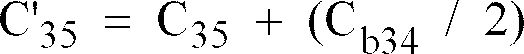
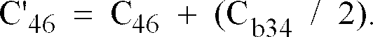
- a capacitor C 35 is connected between t3 (the tip line of pair 3) and t1 (the tip line of pair 1); capacitor C 46 is connected between r1 (the ring line of pair 1) and r3 (the ring line of pair 3); and capacitor C 25 is connected between r2 and r3.
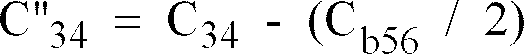
- capacitor C 34 is connected between t3 and r1; capacitor C 56 is connected between t1 and r3; capacitor C 14 is connected between t2 and r1; and capacitor C 37 is connected between t3 and t4.
- a capacitor C 48 is connected between r1 and r4; and a capacitor C 38 is connected between t3 and r4.
- the near-end crosstalk (NEXT) on pairs 1&3 is assumed to be essentially balanced in the plug and the lead-frame due to symmetry.
- the second compensation stage in FIG. 2 is the same as the second compensation stage in FIG. 3.
- C r34 is the capacitance between t3 and r1
- C r34 results in unbalancing the capacitive coupling of pair 1&3 in the third compensation stage of FIG. 2.
- a capacitor C b56 having a value equal to C r34 is added between conductors 5 and 6 in the third compensation stage. Therefore:
- the overall corrected circuit 300 based on this solution is shown in FIG. 3.
- the overall corrected circuit 400 based on this solution is shown in FIG. 4.
- capacitor C 34 is replaced with capacitor C" 34 between t3 and r1
- capacitor C 56 is replaced with capacitor C" 56 between t1 and r3
- C" 34 C 34 - (C b56 / 2)
- C" 56 C 56 - (C b56 / 2).
- the present invention also provides a method 500 for balancing crosstalk in a connector, wherein a compensation scheme in a first pair combination disturbs the crosstalk balance of a second pair combination.
- a compensation scheme in a first pair combination disturbs the crosstalk balance of a second pair combination.
- corrective capacitive devices are added to the second pair combination to compensate for the crosstalk unbalance in the second pair combination.
- Method 500 also includes the step of adjusting the compensating coupling devices in the second pair combination to compensate for crosstalk disturbances caused from the corrective coupling devices in the second pair combination, as depicted in block 520.
- the invention can be applied to any pair combination which has its crosstalk balance disturbed due to interactions from compensation schemes on other pair combinations. It also should be understood that the present invention can be implemented using any type of coupling device (e.g. either capacitors or mutual inductors or both). Furthermore, these devices may be discrete or integral parts of printed wiring boards, lead-frames, or stamped metal conductors, for example.
- coupling device e.g. either capacitors or mutual inductors or both.
- these devices may be discrete or integral parts of printed wiring boards, lead-frames, or stamped metal conductors, for example.
- One of the advantages of the present invention is the lowering of NEXT in communication connecting hardware, which is important for complying with the proposed Category 6 cabling standard by the Telecommunication Industry Association.
- a connector will have to satisfy NEXT requirements from 1 MHz to 250 MHz, whereas poor NEXT performance can cause connectors to degrade by as much as a whole category.
Abstract
Description
- The present invention generally relates to electrical connectors, and more particularly, to connectors designed to compensate for crosstalk induced on a conductor pair from other conductor pairs.
- In conventional electrical communication systems, such as these for telephony and data applications, a balanced signal is transmitted over a communication path composed of a pair of conductors that are not grounded. The balanced, or differential, signal constitutes the voltage difference between the individual conductors in the pair without regard to the absolute voltages present on each conductor. In such conductor pair transmission systems, an electromagnetic field is often created that interferes with signals on adjacent conductors. As the frequency of the transmitted signal increases, the effects of this interference become even greater. This interference is electrical noise and is commonly referred to as crosstalk.
- Crosstalk can occur at any place where conductor pairs are in close proximity. A particular type of crosstalk called near-end crosstalk (NEXT) occurs at the near ends of communication or transmission paths, since the near end of a path may have eight or more wires situated close together over a very short distance.
- NEXT is the portion of a transmitted signal that is electromagnetically coupled back into the received signal. For example, NEXT occurs in telephone communication whenever a separate communication is overheard on a telephone. In the case of computer networks, NEXT occurs when a strong signal on one pair of wires is picked up by an adjacent pair of wires. Two different types of NEXT can be induced in an adjacent pair of conductors, namely, differential-mode crosstalk and common-mode crosstalk.
- Differential-mode crosstalk corresponds to a differential or balanced signal that is induced in the adjacent pair, where the currents in the two wires of that pair flow in opposite directions. Common-mode crosstalk corresponds to a common-mode or an unbalanced signal that is induced in the adjacent pair, where the currents in the two wires of that pair flow in the same direction. When a differential-mode signal exists on one pair, it may induce both differential-mode and common-mode crosstalk on an adjacent wire pair. The actual magnitude for each crosstalk mode is influenced by a number of factors, such as the relative proximities of the individual wires of the pair carrying the signal to the individual wires of the adjacent pair experiencing the crosstalk.
- In attempts to reduce or compensate for NEXT crosstalk in communication paths, compensating signals are often introduced to counteract the effects of the crosstalk disturbances or noise. Such crosstalk compensation is achieved by connecting coupling devices, such as capacitors or capacitance-producing patterns on printed wiring boards, between different pairs of conductors of a multi-pair connector. Customarily, multiple compensation stages are needed because, at high frequencies, crosstalk compensating signals cannot be introduced that are exactly 180 degrees out of phase with the offending crosstalk through utilization of a single compensation stage.
- For example, U.S. Patent No. 5,997,358, issued on December 7, 1999, discloses a multi-stage compensation scheme. In accordance with this scheme, crosstalk compensation is introduced either by creating crossovers of certain conductors within the connector, or by appropriately placing capacitors to compensate for differential-mode crosstalk. U.S. Pat. No. 5,967,853, issued on October 19, 1999, describes a multi-stage compensation scheme that uses capacitors between different pairs of conductors to compensate for both common-mode and differential-mode crosstalk. In U.S. Pat. No. 6,270,381, issued on August 7, 2001, a multi-stage compensation scheme is disclosed that uses crossovers between different pairs of conductors to compensate for common-mode and differential-mode crosstalk.
- Existing crosstalk compensation schemes used with electrical connectors, such as those described above, are designed to compensate for crosstalk induced in a pair of conductors from an adjacent driven pair of conductors. Such existing crosstalk compensation schemes, however, may actually disturb the crosstalk balance of nearby pairs. A heretofore unaddressed need exists in the industry for a system and method that corrects NEXT crosstalk unbalance introduced by crosstalk compensation schemes.
- Accordingly, a need exists to compensate for NEXT unbalance in a pair combination caused by a NEXT compensation scheme deployed on another pair combination. A further need exists for such a compensation technique that could be employed with connectors that are designed to meet the proposed
Category 6 cabling standard set forth by the Telecommunication Industry Association (TIA) task group under TIA/EIA-568-B.2-1 (addendum No. 1 to TIA/EIA-568-B.2). - The present invention overcomes the inadequacies and deficiencies of the prior art as discussed hereinbefore. Generally, the present invention is directed to a system and method for correcting NEXT unbalance in a pair combination generated from a crosstalk compensation scheme on another pair combination in a connector.
- In accordance with one aspect of the present invention, a system for balancing crosstalk in an electrical connector with the following features is provided. The electrical connector has three or more pairs of conductors, wherein two pairs of conductors form a pair combination. The connector also has at least one compensating coupling device connected between the two pairs of conductors in a first pair combination. The compensating coupling device disturbs the crosstalk balance of a second pair combination. Thus, one embodiment of the present invention provides a system to compensate for the crosstalk disturbance in the connector caused by the compensating coupling device. The system includes at least one corrective coupling device connected between the two pairs of conductors in the second pair combination. In addition, one or more compensating coupling devices connected between the two pairs of conductors in the second pair combination are to counteract any crosstalk disturbances caused by one or more of the corrective coupling device.
- In accordance with another aspect of the present invention, a method for balancing crosstalk in an electrical connector with the following features is provided. The electrical connector has three or more pairs of conductors, wherein two pairs of conductors form a pair combination. The connector also has at least one compensating coupling device connected between the two pairs of conductors in a first pair combination. The compensating coupling device disturbs the crosstalk balance of a second pair combination. In this regard, an embodiment of the method can be summarized by the following steps: Adding at least one corrective coupling device between the two pairs of conductors in second pair combination, wherein the corrective coupling device compensates for crosstalk balance disturbances generated by the compensating coupling device in the first pair combination; and adjusting compensating coupling devices in the second pair combination to counteract any crosstalk disturbances caused by the corrective coupling device.
- Other features and advantages of the present invention will become apparent to one with skill in the art upon examination of the following drawings and detailed description.
- The invention can be better understood with reference to the following drawings. The elements of the drawings are not necessarily to scale relative to each other, emphasis instead being placed upon clearly illustrating the principles of the invention. Furthermore, like reference numerals designate corresponding parts throughout the several views.
- FIG. 1 is a schematic drawing representing a known wiring scheme for a modular plug and jack under the TIA T568B specification.
- FIG. 2 is a schematic drawing representing a known differential-mode to differential-mode crosstalk compensation scheme for a modular plug/jack combination of FIG. 1.
- FIG. 3 is a schematic drawing representing an example embodiment of a system of the present invention for correcting crosstalk disturbances caused by a compensation scheme, such as the known compensation scheme of FIG. 2.
- FIG. 4 is a schematic drawing representing another example embodiment of a system of the present invention for correcting crosstalk disturbances caused by a compensation scheme, such as the compensation scheme of FIG. 2.
- FIG. 5 is a flowchart describing an embodiment of a method of the present invention for correcting crosstalk disturbances caused by a compensation scheme, such as the compensation scheme of FIG. 2.
- The present invention provides a system and method for compensating for crosstalk balance in a pair combination whose crosstalk balance has been compromised by the deployment of compensation schemes on other pair combinations. FIG. 1 is a schematic drawing representing the wiring scheme for a known
modular plug 10 andjack 20 under the TIA T568B specification. Consider, for example, pairs 1 (conductors 4 and 5) and 3 (conductors 3 and 6) in FIG. 1. Although the pair combination is originally balanced, the asymmetric placement of capacitive couplings (not shown) aroundpairs pairs 1 and 3) to become compromised. - Now consider FIG. 2, which is a schematic drawing representing a known differential-mode to differential-mode crosstalk compensation scheme for a modular plug/jack combination such as that of FIG. 1. The differential-mode to differential-mode crosstalk compensation scheme of FIG. 2 is a multistage capacitive compensation scheme implemented on a printed wiring board (PWB) that works in complement with a typically inductive lead frame first stage. Principally, compensation coupling devices are connected between conductors to form multistage compensating regions.
- In particular, in the first compensation stage of FIG. 2, a capacitor C35 is connected between t3 (the tip line of pair 3) and t1 (the tip line of pair 1); capacitor C46 is connected between r1 (the ring line of pair 1) and r3 (the ring line of pair 3); and capacitor C25 is connected between r2 and r3. In the second compensation stage, capacitor C34 is connected between t3 and r1; capacitor C56 is connected between t1 and r3; capacitor C14 is connected between t2 and r1; and capacitor C37 is connected between t3 and t4. In the third stage, a capacitor C48 is connected between r1 and r4; and a capacitor C38 is connected between t3 and r4.
- In FIG. 2, the near-end crosstalk (NEXT) on pairs 1&3 is assumed to be essentially balanced in the plug and the lead-frame due to symmetry. The first compensation stage of pairs 1&3 is implemented on the PWB by capacitors C35 and C46 where C35 = C46. However, pairs 1&3 also experience a capacitance between its
conductors 
- Cr56 is the capacitance between t1 and r3. It results in unbalancing the capacitive coupling of pair 1&3, since there is no capacitance to counter it between t3 and r1. To reestablish balance on
pair 1 &3, it has been determined in accordance with the present invention that a capacitor Cb34 having a value equal to Cr56 can be added betweenconductors 
stage 1. This is corrected in accordance with the present invention by augmenting each of C35 and C46 by half of Cb34 so that:

pair 1 &3 that is equal in magnitude and polarity to the pre-correction unbalanced differential-mode to differential-mode compensation for the first compensation stage. - In examining the second compensation stage in FIG. 2, no capacitance appears between the conductors of pairs 1&3 from the capacitive couplings deployed between the conductors of the other pair combinations. Therefore, no correction is needed in the second compensation stage as long as:

- In the third compensation stage of FIG. 2, however, pairs 1&3 experience a capacitance between its
conductors 
- Since Cr34 is the capacitance between t3 and r1, Cr34 results in unbalancing the capacitive coupling of pair 1&3 in the third compensation stage of FIG. 2. There is no capacitance to counter Cr34 between t1 and r3 in the third compensation stage of FIG. 2. To reestablish balance on pair 1&3, a capacitor Cb56 having a value equal to Cr34 is added between
conductors 
- However the addition of Cb56 results in de-compensating the third compensation stage of pair 1&3, which can be corrected by adding capacitors C'''35 and C"'46 each equal to half of Cb56 so that:

circuit 300 based on this solution is shown in FIG. 3. - Therefore, according to one embodiment of the
present invention 300, compensating coupling devices are connected between conductors to compensate for the capacitive unbalance caused by compensation schemes: As shown by FIG. 3, the first compensation stage of FIG. 2 may be balanced by adding a capacitor Cb34 between t3 and r1, replacing capacitor C35 with capacitor C'35 between t3 and t1, and replacing capacitor C46 with capacitor C'46 between r1 and r3, where:

- Further, the second compensation stage of FIG. 3 receives no correction as long as C34 = C56. In the third compensation stage of FIG. 3, balance is achieved by adding capacitor C"'35 between t3 and t1; by adding capacitor Cb56 between t1 and r3; and by adding capacitor C'''46 between r1 and r3, where:


- Alternatively, the decompensation in the third stage of FIG. 3 can be corrected for in the second stage by reducing each of C34 and C56 by half of Cb56 such that:


circuit 400 based on this solution is shown in FIG. 4. - Therefore, according to a second example embodiment of the
present invention 400, compensating coupling devices are connected between conductors to compensate for the capacitive unbalance caused by compensation schemes: As shown by FIG. 4, the first compensation stage of FIG. 2 may be balanced by adding capacitor Cb34 between t3 and r1, replacing capacitor C35 with capacitor C'35 between t3 and t1, and replacing C46 with capacitor C'46 between r1 and r3, where:

- Correspondingly, in the second compensation stage, capacitor C34 is replaced with capacitor C"34 between t3 and r1, and capacitor C56 is replaced with capacitor C"56 between t1 and r3; and in the third compensation stage, Cb56 is added between t1 and r3, where:


- As shown in FIG. 5, the present invention also provides a
method 500 for balancing crosstalk in a connector, wherein a compensation scheme in a first pair combination disturbs the crosstalk balance of a second pair combination. Inblock 510, corrective capacitive devices are added to the second pair combination to compensate for the crosstalk unbalance in the second pair combination.Method 500 also includes the step of adjusting the compensating coupling devices in the second pair combination to compensate for crosstalk disturbances caused from the corrective coupling devices in the second pair combination, as depicted inblock 520. - Although the example above deals with pairs 1&3, the invention can be applied to any pair combination which has its crosstalk balance disturbed due to interactions from compensation schemes on other pair combinations. It also should be understood that the present invention can be implemented using any type of coupling device (e.g. either capacitors or mutual inductors or both). Furthermore, these devices may be discrete or integral parts of printed wiring boards, lead-frames, or stamped metal conductors, for example.
- One of the advantages of the present invention is the lowering of NEXT in communication connecting hardware, which is important for complying with the proposed
Category 6 cabling standard by the Telecommunication Industry Association. To meet theCategory 6 standard, a connector will have to satisfy NEXT requirements from 1 MHz to 250 MHz, whereas poor NEXT performance can cause connectors to degrade by as much as a whole category. - It should be emphasized that the above-described embodiments of the present invention are merely possible examples of implementations, merely set forth for a clear understanding of the principles of the invention. Many variations and modifications may be made to the above-described embodiments of the invention without departing substantially from the principles of the invention. For example, the invention can be applied to any conductor pair combination to balance crosstalk from a plurality of stages in a compensation scheme, using any type of capacitive coupling device, beyond the examples stated in this description. All such modifications and variations are within the scope of this disclosure and the present invention.
Claims (10)
- A system for balancing crosstalk in an electrical connector, the connector having three or more pairs of conductors, wherein two pairs of conductors form a pair combination, at least one compensating coupling device being connected between conductor pairs of a first pair combination, the compensating coupling device disturbing the crosstalk balance of a second pair combination, the system comprising:at least one corrective coupling device connected between conductor pairs of the second pair combination, wherein the corrective coupling device compensates for the crosstalk unbalance in the second pair combination generated from the compensating coupling device in the first pair combination.
- The system of claim 1, wherein the second pair combination has at least one compensating coupling device, and wherein the compensating coupling device in the second pair combination is adjusted to compensate for the crosstalk disturbances caused by the corrective coupling device in the second pair combination.
- The system of claim 1, wherein the corrective coupling device comprises a capacitor.
- The system of claim 1, wherein the corrective coupling device comprises a mutual inductor.
- A system for balancing crosstalk in an electrical connector, the connector having three or more pairs of conductors, wherein two pairs of conductors form a pair combination, at least one compensating coupling device being connected between the conductor pairs of a first pair combination, the compensating coupling device disturbing the crosstalk balance of a second pair combination, the system comprising:means for correcting crosstalk disturbance generated by the first pair combination in the second pair combination.
- A method for balancing crosstalk in a connector, the connector having three or more pairs of conductors, wherein two pairs of conductors form a pair combination, and wherein at least one compensating coupling device is connected between a first pair combination, the compensating coupling device disturbing the crosstalk balance of a second pair combination,
the method comprising the step of:correcting crosstalk disturbance generated by the first pair combination in the second pair combination. - The method of claim 13, wherein the correcting step comprises adding at least one corrective coupling device between the second pair combination, wherein the corrective coupling device compensates for crosstalk unbalance generated by the compensating coupling device in the first pair combination.
- The method of claim 14, wherein the second pair combination has at least one compensating coupling device, and wherein the correcting step further comprises:adjusting the compensating coupling device in the second pair combination to compensate for crosstalk disturbance caused by the corrective coupling device in the second pair combination.
- The method of claim 13, wherein the corrective coupling device comprises integral parts of lead frames.
- The method of claim 13, wherein the corrective coupling device comprises a capacitor.
Applications Claiming Priority (2)
| Application Number | Priority Date | Filing Date | Title |
|---|---|---|---|
| US278323 | 2002-10-23 | ||
| US10/278,323 US6866548B2 (en) | 2002-10-23 | 2002-10-23 | Correcting for near-end crosstalk unbalance caused by deployment of crosstalk compensation on other pairs |
Publications (2)
| Publication Number | Publication Date |
|---|---|
| EP1414115A1 true EP1414115A1 (en) | 2004-04-28 |
| EP1414115B1 EP1414115B1 (en) | 2007-08-01 |
Family
ID=32069327
Family Applications (1)
| Application Number | Title | Priority Date | Filing Date |
|---|---|---|---|
| EP03256703A Expired - Lifetime EP1414115B1 (en) | 2002-10-23 | 2003-10-23 | Correcting for near-end crosstalk unbalance caused by deployment of crosstalk compensation on other pairs |
Country Status (5)
| Country | Link |
|---|---|
| US (1) | US6866548B2 (en) |
| EP (1) | EP1414115B1 (en) |
| KR (1) | KR100984998B1 (en) |
| CA (1) | CA2438738C (en) |
| DE (1) | DE60315233T2 (en) |
Cited By (5)
| Publication number | Priority date | Publication date | Assignee | Title |
|---|---|---|---|---|
| WO2008048467A2 (en) | 2006-10-13 | 2008-04-24 | Adc Gmbh | Connecting hardware with multi-stage inductive and capacitive crosstalk compensation |
| DE102006056001A1 (en) * | 2006-11-24 | 2008-06-12 | Phoenix Contact Gmbh & Co. Kg | Field attachable circular connector for Ethernet |
| US7837513B2 (en) | 2004-04-19 | 2010-11-23 | Belden Cdt (Canada) Inc. | Telecommunications connector |
| WO2011056491A1 (en) * | 2009-11-03 | 2011-05-12 | Panduit Corp. | Communication connector with improved crosstalk compensation |
| CN102119472B (en) * | 2008-08-13 | 2013-10-23 | 泛达公司 | Communications connector with multi-stage compensation |
Families Citing this family (43)
| Publication number | Priority date | Publication date | Assignee | Title |
|---|---|---|---|---|
| US7052328B2 (en) * | 2002-11-27 | 2006-05-30 | Panduit Corp. | Electronic connector and method of performing electronic connection |
| US7265300B2 (en) | 2003-03-21 | 2007-09-04 | Commscope Solutions Properties, Llc | Next high frequency improvement using hybrid substrates of two materials with different dielectric constant frequency slopes |
| US20070099507A1 (en) * | 2003-09-22 | 2007-05-03 | Koji Ohnishi | Electric connector |
| CN1902785A (en) * | 2003-11-21 | 2007-01-24 | 莱维顿制造有限公司 | Patch panel with crosstalk reduction system and method |
| US10680385B2 (en) | 2004-02-20 | 2020-06-09 | Commscope Technologies Llc | Methods and systems for compensating for alien crosstalk between connectors |
| US20050221678A1 (en) | 2004-02-20 | 2005-10-06 | Hammond Bernard Jr | Methods and systems for compensating for alien crosstalk between connectors |
| US7187766B2 (en) | 2004-02-20 | 2007-03-06 | Adc Incorporated | Methods and systems for compensating for alien crosstalk between connectors |
| US7317318B2 (en) * | 2004-04-27 | 2008-01-08 | Fluke Corporation | FEXT cancellation of mated RJ45 interconnect |
| US7190594B2 (en) * | 2004-05-14 | 2007-03-13 | Commscope Solutions Properties, Llc | Next high frequency improvement by using frequency dependent effective capacitance |
| US7980900B2 (en) * | 2004-05-14 | 2011-07-19 | Commscope, Inc. Of North Carolina | Next high frequency improvement by using frequency dependent effective capacitance |
| US7038554B2 (en) * | 2004-05-17 | 2006-05-02 | Leviton Manufacturing Co., Inc. | Crosstalk compensation with balancing capacitance system and method |
| US7402085B2 (en) * | 2006-04-11 | 2008-07-22 | Adc Gmbh | Telecommunications jack with crosstalk compensation provided on a multi-layer circuit board |
| US7787615B2 (en) * | 2006-04-11 | 2010-08-31 | Adc Telecommunications, Inc. | Telecommunications jack with crosstalk compensation and arrangements for reducing return loss |
| US7381098B2 (en) | 2006-04-11 | 2008-06-03 | Adc Telecommunications, Inc. | Telecommunications jack with crosstalk multi-zone crosstalk compensation and method for designing |
| AU2007201113B2 (en) | 2007-03-14 | 2011-09-08 | Tyco Electronics Services Gmbh | Electrical Connector |
| AU2007201114B2 (en) * | 2007-03-14 | 2011-04-07 | Tyco Electronics Services Gmbh | Electrical Connector |
| AU2007201107B2 (en) | 2007-03-14 | 2011-06-23 | Tyco Electronics Services Gmbh | Electrical Connector |
| AU2007201106B9 (en) * | 2007-03-14 | 2011-06-02 | Tyco Electronics Services Gmbh | Electrical Connector |
| AU2007201109B2 (en) | 2007-03-14 | 2010-11-04 | Tyco Electronics Services Gmbh | Electrical Connector |
| AU2007201102B2 (en) * | 2007-03-14 | 2010-11-04 | Tyco Electronics Services Gmbh | Electrical Connector |
| AU2007201105B2 (en) | 2007-03-14 | 2011-08-04 | Tyco Electronics Services Gmbh | Electrical Connector |
| AU2007201108B2 (en) * | 2007-03-14 | 2012-02-09 | Tyco Electronics Services Gmbh | Electrical Connector |
| US7798857B2 (en) * | 2008-02-12 | 2010-09-21 | Adc Gmbh | Asymmetric crosstalk compensation for improved alien crosstalk performance |
| US7841909B2 (en) | 2008-02-12 | 2010-11-30 | Adc Gmbh | Multistage capacitive far end crosstalk compensation arrangement |
| CA2734133C (en) * | 2008-08-20 | 2016-01-05 | Panduit Corp. | High-speed connector with multi-stage compensation |
| KR101040580B1 (en) * | 2008-09-19 | 2011-06-13 | 대한민국 | Raising Seedings of Multistage Apparatus |
| US8145442B2 (en) * | 2009-01-30 | 2012-03-27 | Synopsys, Inc. | Fast and accurate estimation of gate output loading |
| US8016621B2 (en) | 2009-08-25 | 2011-09-13 | Tyco Electronics Corporation | Electrical connector having an electrically parallel compensation region |
| US8435082B2 (en) | 2010-08-03 | 2013-05-07 | Tyco Electronics Corporation | Electrical connectors and printed circuits having broadside-coupling regions |
| US7967644B2 (en) | 2009-08-25 | 2011-06-28 | Tyco Electronics Corporation | Electrical connector with separable contacts |
| US8128436B2 (en) * | 2009-08-25 | 2012-03-06 | Tyco Electronics Corporation | Electrical connectors with crosstalk compensation |
| US8235731B1 (en) * | 2011-03-18 | 2012-08-07 | Leviton Manufacturing Co., Ltd. | Connector module and patch panel |
| KR101105311B1 (en) * | 2011-06-09 | 2012-01-18 | 이용우 | Appratus for cultivating plant |
| CN103947055B (en) | 2011-11-23 | 2017-03-08 | 泛达公司 | Compensation network using quadrature compensation network |
| US9601847B2 (en) * | 2011-12-22 | 2017-03-21 | CommScope Connectivity Spain, S.L. | High density multichannel twisted pair communication system |
| US9136647B2 (en) | 2012-06-01 | 2015-09-15 | Panduit Corp. | Communication connector with crosstalk compensation |
| US9147977B2 (en) | 2012-07-05 | 2015-09-29 | Leviton Manufacturing Co., Inc. | High density high speed data communications connector |
| US9246463B2 (en) | 2013-03-07 | 2016-01-26 | Panduit Corp. | Compensation networks and communication connectors using said compensation networks |
| US9257792B2 (en) | 2013-03-14 | 2016-02-09 | Panduit Corp. | Connectors and systems having improved crosstalk performance |
| US9246274B2 (en) | 2013-03-15 | 2016-01-26 | Panduit Corp. | Communication connectors having crosstalk compensation networks |
| TWI611640B (en) * | 2015-05-22 | 2018-01-11 | 好慶科技企業股份有限公司 | Circuit board |
| CN107949956B (en) * | 2015-09-10 | 2020-11-03 | 泰连德国有限公司 | Contact arrangement and method for reducing crosstalk |
| US11811163B2 (en) | 2021-02-26 | 2023-11-07 | Leviton Manufacturing Co., Inc. | Mutoa and quad floating connector |
Citations (4)
| Publication number | Priority date | Publication date | Assignee | Title |
|---|---|---|---|---|
| US5700167A (en) * | 1996-09-06 | 1997-12-23 | Lucent Technologies | Connector cross-talk compensation |
| US5967853A (en) * | 1997-06-24 | 1999-10-19 | Lucent Technologies Inc. | Crosstalk compensation for electrical connectors |
| US6023200A (en) * | 1997-12-26 | 2000-02-08 | Dae Eun Electric Co., Ltd. | Apparatus for inhibiting cross talk under a difference mode |
| US6089923A (en) * | 1999-08-20 | 2000-07-18 | Adc Telecommunications, Inc. | Jack including crosstalk compensation for printed circuit board |
Family Cites Families (10)
| Publication number | Priority date | Publication date | Assignee | Title |
|---|---|---|---|---|
| CA2072380C (en) * | 1992-06-25 | 2000-08-01 | Michel Bohbot | Circuit assemblies of printed circuit boards and telecommunications connectors |
| GB2271678B (en) * | 1993-12-03 | 1994-10-12 | Itt Ind Ltd | Electrical connector |
| JP3317120B2 (en) * | 1996-01-24 | 2002-08-26 | 住友化学工業株式会社 | Application of asymmetric dioxazine compounds, intermediate compounds thereof and asymmetric dioxazine compounds |
| US5997358A (en) | 1997-09-02 | 1999-12-07 | Lucent Technologies Inc. | Electrical connector having time-delayed signal compensation |
| ES2196580T3 (en) * | 1997-07-10 | 2003-12-16 | Lk As | CONNECTOR TO REDUCE THE COUPLING OF ELECTRICAL SIGNALS AND CABLE EQUIPPED WITH SUCH CONNECTOR. |
| GB2343558B (en) * | 1998-11-04 | 2002-10-30 | Itt Mfg Enterprises Inc | Electrical connector |
| US6533618B1 (en) * | 2000-03-31 | 2003-03-18 | Ortronics, Inc. | Bi-directional balance low noise communication interface |
| US6270381B1 (en) * | 2000-07-07 | 2001-08-07 | Avaya Technology Corp. | Crosstalk compensation for electrical connectors |
| US6379157B1 (en) * | 2000-08-18 | 2002-04-30 | Leviton Manufacturing Co., Inc. | Communication connector with inductive compensation |
| EP1574990B1 (en) * | 2003-12-31 | 2017-11-01 | Dassault Systèmes | Method of editing an explanation model |
-
2002
- 2002-10-23 US US10/278,323 patent/US6866548B2/en not_active Expired - Lifetime
-
2003
- 2003-08-25 CA CA002438738A patent/CA2438738C/en not_active Expired - Fee Related
- 2003-10-23 EP EP03256703A patent/EP1414115B1/en not_active Expired - Lifetime
- 2003-10-23 KR KR1020030074170A patent/KR100984998B1/en not_active IP Right Cessation
- 2003-10-23 DE DE60315233T patent/DE60315233T2/en not_active Expired - Lifetime
Patent Citations (4)
| Publication number | Priority date | Publication date | Assignee | Title |
|---|---|---|---|---|
| US5700167A (en) * | 1996-09-06 | 1997-12-23 | Lucent Technologies | Connector cross-talk compensation |
| US5967853A (en) * | 1997-06-24 | 1999-10-19 | Lucent Technologies Inc. | Crosstalk compensation for electrical connectors |
| US6023200A (en) * | 1997-12-26 | 2000-02-08 | Dae Eun Electric Co., Ltd. | Apparatus for inhibiting cross talk under a difference mode |
| US6089923A (en) * | 1999-08-20 | 2000-07-18 | Adc Telecommunications, Inc. | Jack including crosstalk compensation for printed circuit board |
Cited By (18)
| Publication number | Priority date | Publication date | Assignee | Title |
|---|---|---|---|---|
| US7837513B2 (en) | 2004-04-19 | 2010-11-23 | Belden Cdt (Canada) Inc. | Telecommunications connector |
| US8021197B2 (en) | 2004-04-19 | 2011-09-20 | Belden Cdt (Canada) Inc. | Telecommunications connector |
| US8167656B2 (en) | 2006-10-13 | 2012-05-01 | Adc Gmbh | Connecting hardware with multi-stage inductive and capacitive crosstalk compensation |
| WO2008048467A2 (en) | 2006-10-13 | 2008-04-24 | Adc Gmbh | Connecting hardware with multi-stage inductive and capacitive crosstalk compensation |
| US7537484B2 (en) | 2006-10-13 | 2009-05-26 | Adc Gmbh | Connecting hardware with multi-stage inductive and capacitive crosstalk compensation |
| US8517767B2 (en) | 2006-10-13 | 2013-08-27 | Adc Gmbh | Connecting hardware with multi-stage inductive and capacitive crosstalk compensation |
| US7854632B2 (en) | 2006-10-13 | 2010-12-21 | Adc Gmbh | Connecting hardware with multi-stage inductive and capacitive crosstalk compensation |
| WO2008048467A3 (en) * | 2006-10-13 | 2008-06-05 | Adc Telecommunications Inc | Connecting hardware with multi-stage inductive and capacitive crosstalk compensation |
| US7938650B2 (en) | 2006-11-24 | 2011-05-10 | Phoenix Contact Gmbh & Co. Kg | Manufactured round plug connector for Ethernet |
| DE102006056001B4 (en) * | 2006-11-24 | 2008-12-04 | Phoenix Contact Gmbh & Co. Kg | Field attachable circular connector for Ethernet |
| DE102006056001A1 (en) * | 2006-11-24 | 2008-06-12 | Phoenix Contact Gmbh & Co. Kg | Field attachable circular connector for Ethernet |
| CN102119472B (en) * | 2008-08-13 | 2013-10-23 | 泛达公司 | Communications connector with multi-stage compensation |
| WO2011056491A1 (en) * | 2009-11-03 | 2011-05-12 | Panduit Corp. | Communication connector with improved crosstalk compensation |
| US7985103B2 (en) | 2009-11-03 | 2011-07-26 | Panduit Corp. | Communication connector with improved crosstalk communication |
| US8052483B1 (en) | 2009-11-03 | 2011-11-08 | Panduit Corp. | Communication connector with improved crosstalk connection |
| US8182295B2 (en) | 2009-11-03 | 2012-05-22 | Panduit Corp. | Communication connector with improved crosstalk compensation |
| US8303348B2 (en) | 2009-11-03 | 2012-11-06 | Panduit Corp. | Communication connector with improved crosstalk compensation |
| EP2978081A1 (en) * | 2009-11-03 | 2016-01-27 | Panduit Corp | Communication connector with improved crosstalk compensation |
Also Published As
| Publication number | Publication date |
|---|---|
| US20040082227A1 (en) | 2004-04-29 |
| KR20040036615A (en) | 2004-04-30 |
| DE60315233T2 (en) | 2008-04-17 |
| CA2438738A1 (en) | 2004-04-23 |
| CA2438738C (en) | 2006-01-10 |
| US6866548B2 (en) | 2005-03-15 |
| KR100984998B1 (en) | 2010-10-04 |
| DE60315233D1 (en) | 2007-09-13 |
| EP1414115B1 (en) | 2007-08-01 |
Similar Documents
| Publication | Publication Date | Title |
|---|---|---|
| EP1414115B1 (en) | Correcting for near-end crosstalk unbalance caused by deployment of crosstalk compensation on other pairs | |
| US5967853A (en) | Crosstalk compensation for electrical connectors | |
| US7201618B2 (en) | Controlled mode conversion connector for reduced alien crosstalk | |
| KR101521815B1 (en) | Method and system for reducing common mode signal generation within a plug/jack connection | |
| US6464541B1 (en) | Simultaneous near-end and far-end crosstalk compensation in a communication connector | |
| CA2347985C (en) | Crosstalk compensation for electrical connectors | |
| US7530854B2 (en) | Low noise multiport connector | |
| US9093791B2 (en) | Communications connectors having crosstalk stages that are implemented using a plurality of discrete, time-delayed capacitive and/or inductive components that may provide enhanced insertion loss and/or return loss performance | |
| EP0858684B1 (en) | Reduced cross talk electrical connector | |
| US6533618B1 (en) | Bi-directional balance low noise communication interface | |
| US7154049B2 (en) | Apparatus for crosstalk compensation in a telecommunications connector | |
| US7037140B2 (en) | Dual reactance low noise modular connector insert | |
| US8517767B2 (en) | Connecting hardware with multi-stage inductive and capacitive crosstalk compensation | |
| US20050253662A1 (en) | Crosstalk compensation with balancing capacitance system and method | |
| US20050136729A1 (en) | Patch panel with crosstalk reduction system and method | |
| US20050118881A1 (en) | Low noise communication modular connector insert | |
| KR20100015458A (en) | Plug/jack system having pcb with lattice network | |
| US6816025B2 (en) | Cross talk compensation circuit |
Legal Events
| Date | Code | Title | Description |
|---|---|---|---|
| PUAI | Public reference made under article 153(3) epc to a published international application that has entered the european phase |
Free format text: ORIGINAL CODE: 0009012 |
|
| AK | Designated contracting states |
Kind code of ref document: A1 Designated state(s): AT BE BG CH CY CZ DE DK EE ES FI FR GB GR HU IE IT LI LU MC NL PT RO SE SI SK TR |
|
| AX | Request for extension of the european patent |
Extension state: AL LT LV MK |
|
| 17P | Request for examination filed |
Effective date: 20040610 |
|
| 17Q | First examination report despatched |
Effective date: 20040805 |
|
| AKX | Designation fees paid |
Designated state(s): DE FR GB |
|
| GRAP | Despatch of communication of intention to grant a patent |
Free format text: ORIGINAL CODE: EPIDOSNIGR1 |
|
| RAP1 | Party data changed (applicant data changed or rights of an application transferred) |
Owner name: COMMSCOPE SOLUTIONS PROPERTIES, LLC |
|
| GRAS | Grant fee paid |
Free format text: ORIGINAL CODE: EPIDOSNIGR3 |
|
| GRAA | (expected) grant |
Free format text: ORIGINAL CODE: 0009210 |
|
| AK | Designated contracting states |
Kind code of ref document: B1 Designated state(s): DE FR GB |
|
| REG | Reference to a national code |
Ref country code: GB Ref legal event code: FG4D |
|
| REF | Corresponds to: |
Ref document number: 60315233 Country of ref document: DE Date of ref document: 20070913 Kind code of ref document: P |
|
| ET | Fr: translation filed | ||
| PLBE | No opposition filed within time limit |
Free format text: ORIGINAL CODE: 0009261 |
|
| STAA | Information on the status of an ep patent application or granted ep patent |
Free format text: STATUS: NO OPPOSITION FILED WITHIN TIME LIMIT |
|
| 26N | No opposition filed |
Effective date: 20080506 |
|
| REG | Reference to a national code |
Ref country code: FR Ref legal event code: PLFP Year of fee payment: 13 |
|
| REG | Reference to a national code |
Ref country code: FR Ref legal event code: PLFP Year of fee payment: 14 |
|
| REG | Reference to a national code |
Ref country code: FR Ref legal event code: PLFP Year of fee payment: 15 |
|
| PGFP | Annual fee paid to national office [announced via postgrant information from national office to epo] |
Ref country code: FR Payment date: 20171025 Year of fee payment: 15 Ref country code: DE Payment date: 20171027 Year of fee payment: 15 |
|
| PGFP | Annual fee paid to national office [announced via postgrant information from national office to epo] |
Ref country code: GB Payment date: 20171027 Year of fee payment: 15 |
|
| REG | Reference to a national code |
Ref country code: DE Ref legal event code: R119 Ref document number: 60315233 Country of ref document: DE |
|
| GBPC | Gb: european patent ceased through non-payment of renewal fee |
Effective date: 20181023 |
|
| PG25 | Lapsed in a contracting state [announced via postgrant information from national office to epo] |
Ref country code: DE Free format text: LAPSE BECAUSE OF NON-PAYMENT OF DUE FEES Effective date: 20190501 |
|
| PG25 | Lapsed in a contracting state [announced via postgrant information from national office to epo] |
Ref country code: FR Free format text: LAPSE BECAUSE OF NON-PAYMENT OF DUE FEES Effective date: 20181031 |
|
| PG25 | Lapsed in a contracting state [announced via postgrant information from national office to epo] |
Ref country code: GB Free format text: LAPSE BECAUSE OF NON-PAYMENT OF DUE FEES Effective date: 20181023 |