EP1443418A1 - Architecture for reconfigurable digital signal processor - Google Patents
Architecture for reconfigurable digital signal processor Download PDFInfo
- Publication number
- EP1443418A1 EP1443418A1 EP03425055A EP03425055A EP1443418A1 EP 1443418 A1 EP1443418 A1 EP 1443418A1 EP 03425055 A EP03425055 A EP 03425055A EP 03425055 A EP03425055 A EP 03425055A EP 1443418 A1 EP1443418 A1 EP 1443418A1
- Authority
- EP
- European Patent Office
- Prior art keywords
- array
- configurable
- architecture according
- digital
- processor
- Prior art date
- Legal status (The legal status is an assumption and is not a legal conclusion. Google has not performed a legal analysis and makes no representation as to the accuracy of the status listed.)
- Ceased
Links
Images


Classifications
-
- G—PHYSICS
- G06—COMPUTING; CALCULATING OR COUNTING
- G06F—ELECTRIC DIGITAL DATA PROCESSING
- G06F9/00—Arrangements for program control, e.g. control units
- G06F9/06—Arrangements for program control, e.g. control units using stored programs, i.e. using an internal store of processing equipment to receive or retain programs
- G06F9/30—Arrangements for executing machine instructions, e.g. instruction decode
- G06F9/38—Concurrent instruction execution, e.g. pipeline, look ahead
- G06F9/3885—Concurrent instruction execution, e.g. pipeline, look ahead using a plurality of independent parallel functional units
-
- G—PHYSICS
- G06—COMPUTING; CALCULATING OR COUNTING
- G06F—ELECTRIC DIGITAL DATA PROCESSING
- G06F15/00—Digital computers in general; Data processing equipment in general
- G06F15/76—Architectures of general purpose stored program computers
- G06F15/78—Architectures of general purpose stored program computers comprising a single central processing unit
- G06F15/7867—Architectures of general purpose stored program computers comprising a single central processing unit with reconfigurable architecture
-
- G—PHYSICS
- G06—COMPUTING; CALCULATING OR COUNTING
- G06F—ELECTRIC DIGITAL DATA PROCESSING
- G06F9/00—Arrangements for program control, e.g. control units
- G06F9/06—Arrangements for program control, e.g. control units using stored programs, i.e. using an internal store of processing equipment to receive or retain programs
- G06F9/30—Arrangements for executing machine instructions, e.g. instruction decode
- G06F9/38—Concurrent instruction execution, e.g. pipeline, look ahead
- G06F9/3877—Concurrent instruction execution, e.g. pipeline, look ahead using a slave processor, e.g. coprocessor
-
- G—PHYSICS
- G06—COMPUTING; CALCULATING OR COUNTING
- G06F—ELECTRIC DIGITAL DATA PROCESSING
- G06F9/00—Arrangements for program control, e.g. control units
- G06F9/06—Arrangements for program control, e.g. control units using stored programs, i.e. using an internal store of processing equipment to receive or retain programs
- G06F9/30—Arrangements for executing machine instructions, e.g. instruction decode
- G06F9/38—Concurrent instruction execution, e.g. pipeline, look ahead
- G06F9/3885—Concurrent instruction execution, e.g. pipeline, look ahead using a plurality of independent parallel functional units
- G06F9/3893—Concurrent instruction execution, e.g. pipeline, look ahead using a plurality of independent parallel functional units controlled in tandem, e.g. multiplier-accumulator
- G06F9/3895—Concurrent instruction execution, e.g. pipeline, look ahead using a plurality of independent parallel functional units controlled in tandem, e.g. multiplier-accumulator for complex operations, e.g. multidimensional or interleaved address generators, macros
- G06F9/3897—Concurrent instruction execution, e.g. pipeline, look ahead using a plurality of independent parallel functional units controlled in tandem, e.g. multiplier-accumulator for complex operations, e.g. multidimensional or interleaved address generators, macros with adaptable data path
Definitions
- the present invention relates to an embedded architecture including a microcontroller and a memory device suitable for digital signal processing based on reconfigurable computing.
- the invention may find application in many environments such as in multimedia applications, audio and image compression and decompression standards, security applications such as code encryption and voice/image recognition, and telecommunications protocol management such as TCP/IP and UMTS.
- a further more fine-grain solution provides for a reconfigurability at instruction-set level, also improving the ease of interfacing peripherals.
- Another solution developed by the Company Tensilica, offers a configurable processor "Xtensa” where instructions can be easily added at design time within the pipeline; see in this respect the article by R. E. Gonzales “Xtensa: a configurable and extensible processor” IEEE Micro, Volume: 20 Issue 2, March-April 2000.
- FPGA Field Programmable Gate Array
- the first group includes the GARP processor, known from the article by T. Callahan, J. Hauser, and J. Wawrzynek having title: "The Garp architecture and C compiler” IEEE Computer, 33(4) : 62-69, April 2000.
- a similar architecture is provided by the A-EPIC processor that is disclosed in the article by S. Palem and S. Talla having title: "Adaptive explicit parallel instruction computing", Proceedings of the fourth Australasian COmputer Architecture Conference (ACOAC), January 2001.
- FPGA suppliers such as Altera Corporation offer digital architectures based on the US Patent No. 5,968,161 to T.J. Southgate, "FPGA based configurable CPU additionally including second programmable section for implementation of custom hardware support".
- a relevant drawback in this approach is often the memory data access bottleneck that often forces long stalls on the FPGA device in order to fetch on the shared registers enough data to justify its activation.
- Microlen main advantage is to utilize commercially available FPGA devices to build an embedded reconfigurable architecture that couples existing processor models (Altera Nios, IBM PowerPC) with well known gate-array technology (Altera Apex 20KE, Xilinx Virtex II Pro) obtaining significant performance speed-up for a broad range of DSP algorithms.
- the technical problem of the present invention is that of providing a new kind of embedded digital architecture having functional and structural features capable to offer significant performance and energy consumption enhancements with respect to a traditional signal processing device.
- such a new architecture should provide a programmer-friendly algorithm development environment based on C language while ensuring usual compilation and software evaluation tools.
- the invention overcomes the limitations of similar preceding architectures relying on a reconfigurable device of different nature, and a new approach to processor/gate-array interface.
- the proposed architecture exploits concurrent use of hardwired computational logic and of an additional data elaboration channel comprising a pipelined array of configurable, look-up table based cells controlled by a special purpose control unit.
- the digital architecture previously indicated comprises: a processor, structured to implement a Very Long Instruction Word elaboration mode by a general purpose hardwired computational logic, and an additional data elaboration channel comprising a reconfigurable function unit based on a pipelined array of configurable look-up table based cells controlled by a special purpose control unit, thus easing the elaboration of critical kernels algorithms.
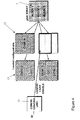
- FIG. 1 a digital embedded architecture realized according to the present invention for digital signal processing based on reconfigurable computing.
- the architecture 1 is schematically shown in Figure 1 and referred hereinafter as "XiRisc" (Extended instruction set RISC).
- the XiRisc architecture 1 comprises a processor 2 and a memory device 3 integrated into a same chip.
- the processor 2 is structured to implement a Very Long Instruction Word (VLIW) RISC architecture featuring two concurrent, pipelined data elaboration channels operating concurrently over a set of general purpose hardwired function units specifically designed to improve its performance in a signal processing application environment.
- VLIW Very Long Instruction Word
- Target applications for the architecture 1 include a relevant collection of signal processing algorithms.
- multimedia applications such as audio and image compression and decompression standards
- security applications such as code encryption and voice/image recognition
- telecommunications protocol management such as TCP/IP and UMTS.
- the present invention focuses on easing the elaboration of such critical kernels, partitioning the computational load that they introduce on two concurrent elaboration cores: the first relying on a standard software-based compilation on a standard digital processor core, and the second focused on hardware programmable logic, to be performed on the cell array.
- the processor 2 is provided with an additional run time configurable data path, capable of introducing a potentially infinite number of virtual application specific function units.
- the data path is tightly integrated in a processor core 3, receiving inputs from a register file 4 and writing results on dedicated write back channels 5, 6 over the register file 4.
- the architecture 1 is thus effectively based on three different and concurrent data elaboration flows, two of which fed each cycle by instruction fetch and one based on an independent, variable latency pipeline implemented on the configurable datapath.
- the instruction set extension is that of a reconfigurable architecture.
- the hardware extension is modeled as any other function unit of the processor 2, fully controlled by assembly instructions that are "in lined" in the source code.
- the reconfigurable function unit (PiCoGa) is not an hardware-based FPGA device but rather a configurable data-path controlled by a dedicated control unit 8.
- the PiCo-Array is a special function unit, comprising a pipelined array of lookup-based, configurable cells especially designed to virtually emulate a microprocessor data path.
- topology of elaboration inside the PiCo-Array is not symmetrical in the two directions: cells are grouped in rows, each representing a possible stage of a customized pipeline.
- the PiCo-Array structure 7 can easily be represented by a Control data flow graph, each row (or group of rows) corresponding to a different state.
- the PiCo-Array pipeline activity is controlled by a dedicated control unit 8.
- the unit 8 generates control signals for each row of the array 7: every clock cycle only the rows involved in the computation phase to be executed in that specific cycle are activated, in a dataflow fashion.
- each array row can generate a feedback signal for the control unit 8, that may represent a Boolean value from a condition check performed in the array core.
- the PiCo-Array 7 does not only support multi-cycle functions, but it is explicitly structured to handle configurable pipelines, even deep ones.
- Each reconfiguration of the array may implement a peculiar data flow, with a number of stages suitable for the functionality to be performed that could even be unknown at compilation time.
- PiCo-Array instructions latency, as well as their results may depend on internal status informations stored in some cell register by previous instructions, thus dramatically reducing the required data throughput on the register file, that was a severe limitations to previous implementations.
- the XiRisc computational model takes advantage of strong synergy between different units tightly integrated in a single core.
- FPGAs behaving as co-processing or function units need to implement entire computational kernels to achieve results that justify the communication overhead due to their inclusion.
- a specific task is composed of functions suitable to be mapped on a hardware-oriented device and operators which could not be efficiently implemented in such devices, it has either to be completely executed on the processor core leaving the FPGA unused or to be entirely re-mapped on the array stalling for long periods processor execution.
- the pipelined approach of the PiCo-Array makes the communication overhead with other function units as small as possible, thus allowing to efficiently partition the operations composing a single task to the function unit that best fit them.
- the configurable unit exploits parallelism of small portions of the task, implementing short-latency, hardware intensive application specific operators. In this way, utilization of the PiCo-Array 7 considerably increases, minimizing program flow stalls and achieving a considerable parallelism between available resources, thus justifying its cost in terms of area for a wide range of applications.
- the XiRisc 32-slots register file features four read ports, that are used to support the issue of two RISC instructions each clock cycle. Two write ports are reserved for the two hardwired pipeline channels 5, 6, while two other ports are entirely dedicated to PiCo-Array 7 results write back, avoiding introduction of dedicated logic handling competition on the register file ports.
- Each pGA-load instruction contains information about:
- a dedicated configuration handling logic 13 reads these information and control the download mechanism. Processor elaboration will be stalled only if A pGA-op operation is issued requiring the same operation that is being configured, otherwise it will continue concurrently on the two hardwired channels 5, 6 or on a different block 12 or context of the array 7.
Abstract
Description
- The present invention relates to an embedded architecture including a microcontroller and a memory device suitable for digital signal processing based on reconfigurable computing.
- The invention may find application in many environments such as in multimedia applications, audio and image compression and decompression standards, security applications such as code encryption and voice/image recognition, and telecommunications protocol management such as TCP/IP and UMTS.
- As is well known by those skilled in this specific technical field, a classic architectural solution to achieve high elaboration performance when dealing with critical algorithmic kernels is to enhance a general purpose microcontroller with application-specific signal processors and peripherals for the most time-critical functions.
- As a matter of fact, in order to achieve sufficient volumes of transactions in presence of standards with a variable level of compliance, these platforms must often be over designed to cover the worst case of all requirements.
- A further more fine-grain solution provides for a reconfigurability at instruction-set level, also improving the ease of interfacing peripherals. Another solution, developed by the Company Tensilica, offers a configurable processor "Xtensa" where instructions can be easily added at design time within the pipeline; see in this respect the article by R. E. Gonzales "Xtensa: a configurable and extensible processor" IEEE Micro, Volume: 20
Issue 2, March-April 2000. - However, the computational logic for new instructions is hardwired at design time with an ASIC-like flow, hence the processor can not be reconfigured after fabrication. This, although very successful, is still an application-specific solution with high non-recurrent engineering costs due to design and mask production.
- An appealing alternative option is that of exploiting a Field Programmable Gate Array (FPGA) technology combining standard processors with embedded FPGA devices. This further solution allows to configure into the FPGA at deployment time exactly the required peripherals, exploiting temporal re-use by dynamically reconfiguring the instruction-set at run time based on the currently executed algorithm.
- This solution is disclosed in the U.S. Patent No. 5,956,5181 to A. De Hon, E. Mirsky, J. Knight, F. Thomas, assigned to the Massachussets Institute of Technology and having title: "Intermediate-grain reconfigurable processing device".
- The existing models for designing FPGA/processor interaction can be grouped in two main categories:
- the FPGA is a co-processor communicating with the main processor through a system bus or a specific I/O channel;
- the FPGA is described as a function unit of the processor pipeline.
- The first group includes the GARP processor, known from the article by T. Callahan, J. Hauser, and J. Wawrzynek having title: "The Garp architecture and C compiler" IEEE Computer, 33(4) : 62-69, April 2000. A similar architecture is provided by the A-EPIC processor that is disclosed in the article by S. Palem and S. Talla having title: "Adaptive explicit parallel instruction computing", Proceedings of the fourth Australasian COmputer Architecture Conference (ACOAC), January 2001.
- In both cases the FPGA is addressed via dedicated instructions, moving data explicitly to and from the processor. Control hardware is kept to a minimum, since no interlocks are needed to avoid hazards, but a significant overhead in clock cycles is required to implement communication.
- Only when the number of cycles per execution of the FPGA is relatively high, the communication overhead may be considered negligible.
- In the commercial world, FPGA suppliers such as Altera Corporation offer digital architectures based on the US Patent No. 5,968,161 to T.J. Southgate, "FPGA based configurable CPU additionally including second programmable section for implementation of custom hardware support".
- Other suppliers (Xilinx, Triscend) offer chips containing a processor embedded on the same silicon IC with embedded FPGA logic. See for instance the US Patent 6,467,009 to S.P. Winegarden et al., "Configurable Processor System Unit", assigned to Triscend Corporation.
- However, those chips are generally loosely coupled by a high speed dedicated bus, performing as two separate execution units rather than being merged in a single architectural entity. In this manner the FPGA does not have direct access to the processor memory subsystem, which is one of the strengths of academic approaches outlined above.
- In the second category (FPGA as a function unit) we find some disclosed architectures known as:
- "PRISC" by R. Razdan and M. Smith "A high-performance microarchitecture with hardware-programmable functional units" Proceedings of the 27th Annual International Symposium on Microarchitecture, November 1994;
- "Chimaera" by Z.A. Ye, A. Moshovos, S. Hauck, P. Banerjee "Chimaera: A High-Performance Architecture with Tightly-Coupled Reconfigurable Functional Unit" Proceedings of the 27th International Symposium on Computer Architecture, 2000 Page(s): 225 -235;
- "ConCISe" by B. Kastrup, A. Bink, and J. Hoogerbrugge "ConCISe: A compiler-driven CPLD-based instruction set accelerator" Proceedings of the Seventh Annual IEEE Symposium on Field-Programmable Custom Computing Machines, April 1999.
- In all these models, data are read and written directly on the processor register file minimizing overhead due to communication. In most cases, to minimize control logic and hazard handling and to fit in the processor pipeline stages, the FPGA is limited to combinatorial logic only, thus severely limiting the performance boost that can be achieved.
- Later attempts, like the "OneChip" solution by R. Wittig, and P. Chow "OneChip: An FPGA Processor With Reconfigurable Logic Proceedings" disclosed in the IEEE Symposium on Field-Programmable Custom Computing Machines, pp. 126-135, Napa Valley, California, March 1996, or the processor architectures proposed in the already cited US patents Nos. 5,956,5181 and 6,026,481 address the communication problem effectively sharing registers between a processor core and an independently embedded FPGA device.
- These solutions represent a significant step toward a low-overhead interface between the two entities. Nevertheless, due to the granularity of FPGA operations and its hardware oriented structure, their approach is still very coarse-grained, reducing the possible resource usage parallelism and again including hardware issues not familiar nor friendly to software compilation tools and algorithm developers.
- Thus, a relevant drawback in this approach is often the memory data access bottleneck that often forces long stalls on the FPGA device in order to fetch on the shared registers enough data to justify its activation.
- A more recent architecture exploiting a remarkable trade-off between the models above cited is known as "Molen" processor, developed at the TUDelft; see in this respect the article: "The MOLEN rm-coded Processor", Proceedings of the 11th International Conference on Field-Programmable Logic and Applications 2001 (FPL2001), Belfast, Northern Ireland, UK, August 2001.
- "Molen" main advantage is to utilize commercially available FPGA devices to build an embedded reconfigurable architecture that couples existing processor models (Altera Nios, IBM PowerPC) with well known gate-array technology (Altera Apex 20KE, Xilinx Virtex II Pro) obtaining significant performance speed-up for a broad range of DSP algorithms.
- However, even this solution presents some drawbacks due to the fact that the extension to the processor instruction set are designed by the architecture designers, and "microcoded" in the architecture itself, rather than developed at compilation time by the user.
- Moreover, due to the coarse grain of the tasks involved in the instruction set extension, the size of the introduced reconfigurable logic can severely affect the energy consuption for a given algorithm.
- The technical problem of the present invention is that of providing a new kind of embedded digital architecture having functional and structural features capable to offer significant performance and energy consumption enhancements with respect to a traditional signal processing device.
- Moreover, such a new architecture should provide a programmer-friendly algorithm development environment based on C language while ensuring usual compilation and software evaluation tools.
- The invention overcomes the limitations of similar preceding architectures relying on a reconfigurable device of different nature, and a new approach to processor/gate-array interface. The proposed architecture exploits concurrent use of hardwired computational logic and of an additional data elaboration channel comprising a pipelined array of configurable, look-up table based cells controlled by a special purpose control unit.
- According to a first embodiment of the invention, the digital architecture previously indicated comprises: a processor, structured to implement a Very Long Instruction Word elaboration mode by a general purpose hardwired computational logic, and an additional data elaboration channel comprising a reconfigurable function unit based on a pipelined array of configurable look-up table based cells controlled by a special purpose control unit, thus easing the elaboration of critical kernels algorithms.
- The features and advantages of the digital architecture according to this invention will become apparent from the following description of a best mode for carrying out the invention given by way of non-limiting example with reference to the enclosed drawings.
-
- Figure 1 is a block diagram of a digital architecture for digital signal processing according to the present invention;
- Figure 2 is a block diagram of a hardware register locking mechanism of a register file incorporated into the architecture of Figure 1;
- Figure 3 is a schematic view of a special configuration cache added to the architecture of Figure 1;
- Figure 4 is a block diagram of a detailed view of a particular gate array structure included into the architecture of Figure 1.
-
- With reference to the drawings views, generally shown at 1 is a digital embedded architecture realized according to the present invention for digital signal processing based on reconfigurable computing.
- The
architecture 1 is schematically shown in Figure 1 and referred hereinafter as "XiRisc" (Extended instruction set RISC). - The XiRisc
architecture 1 comprises aprocessor 2 and amemory device 3 integrated into a same chip. Theprocessor 2 is structured to implement a Very Long Instruction Word (VLIW) RISC architecture featuring two concurrent, pipelined data elaboration channels operating concurrently over a set of general purpose hardwired function units specifically designed to improve its performance in a signal processing application environment. - Target applications for the
architecture 1 include a relevant collection of signal processing algorithms. For instance, the main environments where the proposedarchitecture 1 may offer valuable advantages are multimedia applications such as audio and image compression and decompression standards, security applications such as code encryption and voice/image recognition, and telecommunications protocol management such as TCP/IP and UMTS. - A detailed analysis of the cited algorithms could explain how the computational load that they require is not uniformly distributed. For instance, small and very critical kernels, that can be described by few lines with high level programming languages, often require huge portions of overall processing time and energy, while all the many others functionalities composing the algorithm, albeit critical to its completion, become negligible in terms of resource utilization.
- The present invention focuses on easing the elaboration of such critical kernels, partitioning the computational load that they introduce on two concurrent elaboration cores: the first relying on a standard software-based compilation on a standard digital processor core, and the second focused on hardware programmable logic, to be performed on the cell array.
- The
processor 2 is provided with an additional run time configurable data path, capable of introducing a potentially infinite number of virtual application specific function units. - The data path is tightly integrated in a
processor core 3, receiving inputs from aregister file 4 and writing results on dedicated write backchannels register file 4. Thearchitecture 1 is thus effectively based on three different and concurrent data elaboration flows, two of which fed each cycle by instruction fetch and one based on an independent, variable latency pipeline implemented on the configurable datapath. - The instruction set extension is that of a reconfigurable architecture. The hardware extension is modeled as any other function unit of the
processor 2, fully controlled by assembly instructions that are "in lined" in the source code. - Manual identification of the extracted computational kernels is provided too.
- The main difference between the proposed invention and others previously described architectures is that the reconfigurable function unit (PiCoGa) is not an hardware-based FPGA device but rather a configurable data-path controlled by a
dedicated control unit 8. - All the known solution including just an hardware based embedded FPGA may have two possible drawbacks:
- FPGA usage and programming involves hardware development issues not usual to compilation tools and users proficient in high level languages;
- Up to now, FPGA-based units are either hardware based devices that involve a large silicon area, a relevant energy consumption and heavy reanalysis of the target algorithms in order to be executed on the array, or small units that are not capable to handle efficiency multi cycle latency instructions, and are often limited to combinatorial elaboration only, severely restricting the possible application domains.
- However, a specific special purpose and configurable gate-
array 7 has been advantageously provided in the present invention to handle configurable pipelines of data. Hereinafter, we will make reference to this specific array as "PiCo-Array", or Pipelined-Configurable-Array. - Rather than being some kind of embedded, programmable hardware logic array, the PiCo-Array according to this invention is a special function unit, comprising a pipelined array of lookup-based, configurable cells especially designed to virtually emulate a microprocessor data path.
- More specifically, topology of elaboration inside the PiCo-Array is not symmetrical in the two directions: cells are grouped in rows, each representing a possible stage of a customized pipeline.
- The PiCo-
Array structure 7 can easily be represented by a Control data flow graph, each row (or group of rows) corresponding to a different state. - Differently from all existing configurable devices, the PiCo-Array pipeline activity is controlled by a
dedicated control unit 8. Theunit 8 generates control signals for each row of the array 7: every clock cycle only the rows involved in the computation phase to be executed in that specific cycle are activated, in a dataflow fashion. - In order to support implementation of high level language constructions such as while and for loops, each array row can generate a feedback signal for the
control unit 8, that may represent a Boolean value from a condition check performed in the array core. - For this reason, the PiCo-
Array 7 does not only support multi-cycle functions, but it is explicitly structured to handle configurable pipelines, even deep ones. - Each reconfiguration of the array may implement a peculiar data flow, with a number of stages suitable for the functionality to be performed that could even be unknown at compilation time. In fact, PiCo-Array instructions latency, as well as their results may depend on internal status informations stored in some cell register by previous instructions, thus dramatically reducing the required data throughput on the register file, that was a severe limitations to previous implementations.
- Let's now take in consideration the computational model adopted for the present invention.
- The XiRisc computational model takes advantage of strong synergy between different units tightly integrated in a single core.
- In the prior art solutions, FPGAs behaving as co-processing or function units need to implement entire computational kernels to achieve results that justify the communication overhead due to their inclusion. As a consequence, when a specific task is composed of functions suitable to be mapped on a hardware-oriented device and operators which could not be efficiently implemented in such devices, it has either to be completely executed on the processor core leaving the FPGA unused or to be entirely re-mapped on the array stalling for long periods processor execution.
- On the contrary, in the inventive model, the pipelined approach of the PiCo-Array makes the communication overhead with other function units as small as possible, thus allowing to efficiently partition the operations composing a single task to the function unit that best fit them.
- System control, memory and I/O interface, and general purpose arithmetics are performed on the two
hardwired channels - The configurable unit exploits parallelism of small portions of the task, implementing short-latency, hardware intensive application specific operators. In this way, utilization of the PiCo-
Array 7 considerably increases, minimizing program flow stalls and achieving a considerable parallelism between available resources, thus justifying its cost in terms of area for a wide range of applications. - The XiRisc 32-slots register file features four read ports, that are used to support the issue of two RISC instructions each clock cycle. Two write ports are reserved for the two
hardwired pipeline channels Array 7 results write back, avoiding introduction of dedicated logic handling competition on the register file ports. - Given the unpredictable latency of PiCo-
Array instructions 10, Read-After-Write (RAW) hazards may occur on the destination registers of such instructions. - An hardware register locking mechanism, shown in Figure 2, has been introduced as the least intrusive way to handle such hazards. When a PiCo-
Array instruction 10 is decoded its destination registers are locked, so that any following instruction trying to access them will cause a processor stall. - Normal execution is restored only when the PiCo-Array completes the write-
back operation 9, unlocking its destination registers. - For all kinds of reconfigurable architectures described so far, a very critical issue is the programming of the embedded configurable device. The reconfiguration of a
gate array 7 can take hundreds to thousands of cycles, depending on the programmed region size. - Even in cases when elaboration can in principle continue concurrently on other processor resources, the scheduling of the program flow will hardly be able to feed enough instructions to avoid stalls, that could overcome the benefits deriving from the use of the array. In the inventive digital architecture, three different approaches have been adopted to overcome these limitations.
- 1. Multi-context programming: The PiCo-
Array 7 is provided with a first level cache, storing four configurations for each logic cell. Context switch takes only one clock cycle, providing four immediately available instructions. - 2. Region partitioning: The
array 7 is structured in blocks of dynamically variable size 12 (shown in Figure 4). Ablock 12 can be reprogrammed whileother blocks 12 are under execution, so that careful scheduling of operations and reconfigurations may result in no cache miss penalties even when the number of used configurations is large. - 3. Configuration cache: In order to support complete concurrency
between
processor 2 execution and PiCo-Array 7 programming, a special configuration cache is added to thearchitecture 1, featuring a dedicated very large (192-bit) bus to the array. Compression techniques are also used to reduce both size and time of configuration. The configuration process is triggered by the issue of a pGA-load instruction (see figure 3). -
- All possible p-array operations are identified by a pGA-op code, whose length is not fixed (minimum six bits). Each pGA-load instruction contains information about:
- A) the configuration to be loaded into the array and its location in the configuration cache,
- B) the cache context (first level caching) and the block where the operation is to be downloaded. These information can be either stored in one of the processor registers 4, that is referenced by bits [25 .. 21] of the instruction, or be expressed directly in bits [25 ..20] as an immediate operand.
-
- A dedicated
configuration handling logic 13 reads these information and control the download mechanism. Processor elaboration will be stalled only if A pGA-op operation is issued requiring the same operation that is being configured, otherwise it will continue concurrently on the twohardwired channels different block 12 or context of thearray 7. - In any case, once the configuration has completed, elaboration will restart without altering program flow consistency. In case another pGA-load instruction is issued before the previous has finished its process (as introduced before, configuration lasts some hundred cycles depending on the required functionality) no stall occurs: the new pGA-load will be queued in a FIFO memory, and will be performed at the end of the current process.
- If the FIFO queue is full, elaboration is stalled. Only In case a pGA-op instructions refers to a functionality that is neither loaded nor scheduled on the queue an "illegal op-code" exception is raised.
- The advantages of the digital architecture according to the invention may be summarized in the following features:
- Performance enhancement:
- the reconfigurable unit allows for a very efficient implementation of software computational kernels, effectively decreasing the number of cycle required for the completion of a given algorithm, achieving speedup figures from 2x to 13x with respect to a standard programmable device.
-
- Energy consumption minimization:
- the mapping of computational cores on the reconfigurable unit allows for a significant minimization of the main sources of power consumption in programmable architectures, that is instruction fetch and access to the register file. Overall energy consumption figures up to 10% with respect to a standard programmable device depending on the algorithm computed.
-
- Familiar environment for high level languages programmers:
- the pipelined structure of the PiCo-Array and the assembly-level granularity of tasks that are implemented on the array maintains a friendly environment for algorithmic development that do not necessary involves hardware related skills.
-
- Portability to high level software development tools:
- the function unit model of the PiCo-Array/processor interface and the DFG-flow based pipeline control unit make the mapping of software kernels on the configurable unit straightforward for a standard C compiler, that can also take into account scheduling informations to enhance at compilation time instruction-level parallelism.
-
- Very high resource parallelism:
- the VLIW configuration, the presence of DSPspecific hardwired function units and the processor/ gate-array interface allows for a very high level of parallelism in computation. In particular, processor stalls due to interlocks and to the reconfiguration process are significantly less with respect to existing reconfigurable architectures.
-
- Better overall performances over the prior art solutions:
- in the prior art solutions no explicit pipeline handling device is embedded in the configurable device to handle data flow on a software-based fashion. On the contrary, in the invention the gate-array configuration is based on a logic synthesis approach, rather then using high-level languages constructs, that would be more familiar to the user and easier to be handled with high-level language like C.
-
Claims (14)
- A digital embedded architecture (1), including a microcontroller and a memory device, suitable for reconfigurable computing in digital signal processing and comprising: a processor (2), structured to implement a Very Long Instruction Word elaboration mode by a general purpose hardwired computational logic, and an additional data elaboration channel (5, 6) comprising a reconfigurable function unit based on a pipelined array (7) of configurable look-up table based cells controlled by a special purpose control unit (8), thus easing the elaboration of critical kernels algorithms.
- A digital embedded architecture according to claim 1, wherein said reconfigurable function unit includes a hardware-based Field Programmable Gate Array (FPGA) embedded devices.
- A digital embedded architecture according to claim 1, wherein said additional data elaboration channel is tightly integrated in a processor core (3), receiving inputs from a register file (4) and writing results on dedicated write back channels (5, 6) over the register file (4).
- A digital embedded architecture according to claim 1, wherein said pipelined array (7) of configurable lookup-table based cells implements a configurable run-time with a variable latency data path capable to emulate a potentially infinite number of virtual application specific function units.
- A digital embedded architecture according to claim 4, wherein the architecture (1) is based on three different and concurrent data elaboration flows, two of which (5, 6) feed each cycle by instruction fetch and one (7) based on an independent, variable latency pipeline implemented on the configurable data-path.
- A digital embedded architecture according to claim 2, wherein said configurable gate-array (7) is a Pipelined-Configurable-Array (PiCo-Array) comprising a pipelined array of configurable lookup-table based cells virtually emulating a microprocessor data path.
- A digital embedded architecture according to claim 6, wherein the cells of said (PiCo-Array) structure (7) are grouped in rows, each representing a possible stage of a customized pipeline, and the whole array can be represented by a Control data flow graph, each row or group of rows corresponding to a different state.
- A digital embedded architecture according to claim 3, wherein at any decoded instruction (10) of the pipelined array (7) a corresponding destination register file (4) is locked, so that any following instruction trying to access such a register will cause a processor (2) stall; normal execution being restored only when the pipelined array (7) completes the write-back operation unlocking its destination register.
- A digital embedded architecture according to claim 3, wherein said special purpose control unit (8) is a hardwired, run-time programmable Data-Flow-Graph (DFG) based control unit synchronizing the pipelined computation of the gate-array (7) cells.
- A digital embedded architecture according to claim 8, wherein the locking mechanism of said register file (4) supports the highest possible level of resource utilization parallelism allowing unpredictable latency instructions to be executed on the configurable unit without altering program flow consistency.
- A digital embedded architecture according to claim 3, wherein said register file (4) comprises four read ports, used to support the issue of two RISC instructions each clock cycle, and two write ports reserved for said two hardwired pipeline channels (5, 6); two other ports being entirely dedicated to write back results of the pipelined array (7), thus avoiding introduction of dedicated logic handling competition on the register file ports.
- A digital embedded architecture according to claim 1, wherein said pipelined array (7) is provided with a first level cache, storing four configurations for each logic cell; context switch being provided for taking only one clock cycle and providing four immediately available instructions.
- A digital embedded architecture according to claim 1, wherein a specific extension of the instruction set architecture is provided for controlling configuration and execution over the configurable array (7), said instruction set architecture including 32-bit and 64-bit instructions taking advantage of the entire VLIW instruction word.
- A digital embedded architecture according to claim 1, wherein a special purpose reconfiguration mechanism is provided for allowing very fast configuration completely concurrent with processor (2) execution, said reconfiguration mechanism including the configurable array (7) being structured in blocks (12), having at least eight rows each, each block (12) being reprogrammed while the other blocks (12) are under execution.
Priority Applications (2)
| Application Number | Priority Date | Filing Date | Title |
|---|---|---|---|
| EP03425055A EP1443418A1 (en) | 2003-01-31 | 2003-01-31 | Architecture for reconfigurable digital signal processor |
| US10/770,122 US7225319B2 (en) | 2003-01-31 | 2004-02-02 | Digital architecture for reconfigurable computing in digital signal processing |
Applications Claiming Priority (1)
| Application Number | Priority Date | Filing Date | Title |
|---|---|---|---|
| EP03425055A EP1443418A1 (en) | 2003-01-31 | 2003-01-31 | Architecture for reconfigurable digital signal processor |
Publications (1)
| Publication Number | Publication Date |
|---|---|
| EP1443418A1 true EP1443418A1 (en) | 2004-08-04 |
Family
ID=32605501
Family Applications (1)
| Application Number | Title | Priority Date | Filing Date |
|---|---|---|---|
| EP03425055A Ceased EP1443418A1 (en) | 2003-01-31 | 2003-01-31 | Architecture for reconfigurable digital signal processor |
Country Status (2)
| Country | Link |
|---|---|
| US (1) | US7225319B2 (en) |
| EP (1) | EP1443418A1 (en) |
Cited By (3)
| Publication number | Priority date | Publication date | Assignee | Title |
|---|---|---|---|---|
| WO2006092556A2 (en) * | 2005-03-03 | 2006-09-08 | Clearspeed Technology Plc | Reconfigurable logic in processors |
| ITMI20082354A1 (en) * | 2008-12-30 | 2010-06-30 | St Microelectronics Srl | DIGITAL ARCHITECTURE AND RELATED METHOD OF CALCULATION FOR RECONFIGURABLE CALCULATION IN DIGITAL SIGNAL PROCESSING |
| CN111400986A (en) * | 2020-02-19 | 2020-07-10 | 西安智多晶微电子有限公司 | Integrated circuit computing device and computing processing system |
Families Citing this family (14)
| Publication number | Priority date | Publication date | Assignee | Title |
|---|---|---|---|---|
| GB0215034D0 (en) * | 2002-06-28 | 2002-08-07 | Critical Blue Ltd | Architecture generation method |
| JP2008059066A (en) * | 2006-08-29 | 2008-03-13 | Matsushita Electric Ind Co Ltd | Compiler apparatus and semiconductor integrated circuit device |
| US8875199B2 (en) | 2006-11-13 | 2014-10-28 | Cisco Technology, Inc. | Indicating picture usefulness for playback optimization |
| US8156313B2 (en) * | 2007-09-22 | 2012-04-10 | Navosha Corporation | Chained operation of functional units in integrated circuit by writing DONE/complete value and by reading as GO/start value from same memory location |
| US8718388B2 (en) | 2007-12-11 | 2014-05-06 | Cisco Technology, Inc. | Video processing with tiered interdependencies of pictures |
| US7970790B2 (en) * | 2008-05-13 | 2011-06-28 | Microsoft Corporation | Cell-based security representation for data access |
| US8705631B2 (en) | 2008-06-17 | 2014-04-22 | Cisco Technology, Inc. | Time-shifted transport of multi-latticed video for resiliency from burst-error effects |
| US8320465B2 (en) | 2008-11-12 | 2012-11-27 | Cisco Technology, Inc. | Error concealment of plural processed representations of a single video signal received in a video program |
| CN102073481B (en) * | 2011-01-14 | 2013-07-03 | 上海交通大学 | Multi-kernel DSP reconfigurable special integrated circuit system |
| US10407831B2 (en) * | 2014-09-04 | 2019-09-10 | Kemira Oyj | Sizing composition, its use and a method for producing paper, board or the like |
| US10185699B2 (en) | 2016-03-14 | 2019-01-22 | Futurewei Technologies, Inc. | Reconfigurable data interface unit for compute systems |
| US10229470B2 (en) * | 2016-08-05 | 2019-03-12 | Intel IP Corporation | Mechanism to accelerate graphics workloads in a multi-core computing architecture |
| WO2020117346A1 (en) | 2018-12-07 | 2020-06-11 | Water Gremlin Company | Battery parts having solventless acid barriers and associated systems and methods |
| US11422812B2 (en) * | 2019-06-25 | 2022-08-23 | Advanced Micro Devices, Inc. | Method and apparatus for efficient programmable instructions in computer systems |
Citations (3)
| Publication number | Priority date | Publication date | Assignee | Title |
|---|---|---|---|---|
| US5648732A (en) * | 1995-10-04 | 1997-07-15 | Xilinx, Inc. | Field programmable pipeline array |
| US6052773A (en) * | 1995-02-10 | 2000-04-18 | Massachusetts Institute Of Technology | DPGA-coupled microprocessors |
| US20020083308A1 (en) * | 2000-12-20 | 2002-06-27 | Bernardo De Oliveira Kastrup Pereira | Data processing device with a configurable functional unit |
Family Cites Families (6)
| Publication number | Priority date | Publication date | Assignee | Title |
|---|---|---|---|---|
| WO1996034346A1 (en) | 1995-04-28 | 1996-10-31 | Xilinx, Inc. | Microprocessor with distributed registers accessible by programmable logic device |
| US5956518A (en) | 1996-04-11 | 1999-09-21 | Massachusetts Institute Of Technology | Intermediate-grain reconfigurable processing device |
| US5968161A (en) | 1996-08-29 | 1999-10-19 | Altera Corporation | FPGA based configurable CPU additionally including second programmable section for implementation of custom hardware support |
| WO1999056249A1 (en) * | 1998-04-27 | 1999-11-04 | Interactive Silicon, Inc. | Graphics system and method for rendering independent 2d and 3d objects |
| US6467009B1 (en) | 1998-10-14 | 2002-10-15 | Triscend Corporation | Configurable processor system unit |
| JP3636986B2 (en) * | 2000-12-06 | 2005-04-06 | 松下電器産業株式会社 | Semiconductor integrated circuit |
-
2003
- 2003-01-31 EP EP03425055A patent/EP1443418A1/en not_active Ceased
-
2004
- 2004-02-02 US US10/770,122 patent/US7225319B2/en active Active
Patent Citations (3)
| Publication number | Priority date | Publication date | Assignee | Title |
|---|---|---|---|---|
| US6052773A (en) * | 1995-02-10 | 2000-04-18 | Massachusetts Institute Of Technology | DPGA-coupled microprocessors |
| US5648732A (en) * | 1995-10-04 | 1997-07-15 | Xilinx, Inc. | Field programmable pipeline array |
| US20020083308A1 (en) * | 2000-12-20 | 2002-06-27 | Bernardo De Oliveira Kastrup Pereira | Data processing device with a configurable functional unit |
Non-Patent Citations (1)
| Title |
|---|
| SCHMIT H: "Incremental reconfiguration for pipelined applications", FIELD-PROGRAMMABLE CUSTOM COMPUTING MACHINES, 1997. PROCEEDINGS., THE 5TH ANNUAL IEEE SYMPOSIUM ON NAPA VALLEY, CA, USA 16-18 APRIL 1997, LOS ALAMITOS, CA, USA,IEEE COMPUT. SOC, US, 16 April 1997 (1997-04-16), pages 47 - 55, XP010247467, ISBN: 0-8186-8159-4 * |
Cited By (5)
| Publication number | Priority date | Publication date | Assignee | Title |
|---|---|---|---|---|
| WO2006092556A2 (en) * | 2005-03-03 | 2006-09-08 | Clearspeed Technology Plc | Reconfigurable logic in processors |
| WO2006092556A3 (en) * | 2005-03-03 | 2006-12-21 | Clearspeed Technology Plc | Reconfigurable logic in processors |
| ITMI20082354A1 (en) * | 2008-12-30 | 2010-06-30 | St Microelectronics Srl | DIGITAL ARCHITECTURE AND RELATED METHOD OF CALCULATION FOR RECONFIGURABLE CALCULATION IN DIGITAL SIGNAL PROCESSING |
| CN111400986A (en) * | 2020-02-19 | 2020-07-10 | 西安智多晶微电子有限公司 | Integrated circuit computing device and computing processing system |
| CN111400986B (en) * | 2020-02-19 | 2024-03-19 | 西安智多晶微电子有限公司 | Integrated circuit computing equipment and computing processing system |
Also Published As
| Publication number | Publication date |
|---|---|
| US20050015573A1 (en) | 2005-01-20 |
| US7225319B2 (en) | 2007-05-29 |
Similar Documents
| Publication | Publication Date | Title |
|---|---|---|
| EP3449357B1 (en) | Scheduler for out-of-order block isa processors | |
| US7225319B2 (en) | Digital architecture for reconfigurable computing in digital signal processing | |
| EP1877927B1 (en) | Reconfigurable instruction cell array | |
| US7840777B2 (en) | Method and apparatus for directing a computational array to execute a plurality of successive computational array instructions at runtime | |
| Lodi et al. | A VLIW processor with reconfigurable instruction set for embedded applications | |
| US6052773A (en) | DPGA-coupled microprocessors | |
| US20190004878A1 (en) | Processors, methods, and systems for a configurable spatial accelerator with security, power reduction, and performace features | |
| Kastrup et al. | ConCISe: A compiler-driven CPLD-based instruction set accelerator | |
| KR101713815B1 (en) | A tile-based processor architecture model for high efficiency embedded homogeneous multicore platforms | |
| Khawam et al. | The reconfigurable instruction cell array | |
| Glossner et al. | The sandbridge sb3011 platform | |
| US20220100680A1 (en) | Apparatuses, methods, and systems for a configurable accelerator having dataflow execution circuits | |
| Li et al. | Time-multiplexed FPGA overlay architectures: A survey | |
| GB2423840A (en) | Reconfigurable logic in processors | |
| Pasha et al. | System-level synthesis for wireless sensor node controllers: A complete design flow | |
| Nowatzki et al. | Heterogeneous von Neumann/dataflow microprocessors | |
| Rutzig et al. | A transparent and energy aware reconfigurable multiprocessor platform for simultaneous ILP and TLP exploitation | |
| GB2382175A (en) | Reconfigurable processor | |
| Koenig et al. | A scalable microarchitecture design that enables dynamic code execution for variable-issue clustered processors | |
| Fl et al. | Dynamic Reconfigurable Architectures and Transparent Optimization Techniques: Automatic Acceleration of Software Execution | |
| Sangireddy et al. | Low-power high-performance reconfigurable computing cache architectures | |
| Danek et al. | Increasing the level of abstraction in FPGA-based designs | |
| Ackland et al. | A new generation of DSP architectures | |
| Ebeling | The general RaPiD architecture description | |
| Iqbal et al. | Run-time reconfigurable instruction set processor design: Rt-risp |
Legal Events
| Date | Code | Title | Description |
|---|---|---|---|
| PUAI | Public reference made under article 153(3) epc to a published international application that has entered the european phase |
Free format text: ORIGINAL CODE: 0009012 |
|
| AK | Designated contracting states |
Kind code of ref document: A1 Designated state(s): AT BE BG CH CY CZ DE DK EE ES FI FR GB GR HU IE IT LI LU MC NL PT SE SI SK TR |
|
| AX | Request for extension of the european patent |
Extension state: AL LT LV MK RO |
|
| 17P | Request for examination filed |
Effective date: 20050126 |
|
| AKX | Designation fees paid |
Designated state(s): DE FR GB IT |
|
| RBV | Designated contracting states (corrected) |
Designated state(s): DE FR GB IT |
|
| 17Q | First examination report despatched |
Effective date: 20050929 |
|
| RAP1 | Party data changed (applicant data changed or rights of an application transferred) |
Owner name: STMICROELECTRONICS SRL |
|
| STAA | Information on the status of an ep patent application or granted ep patent |
Free format text: STATUS: THE APPLICATION HAS BEEN REFUSED |
|
| 18R | Application refused |
Effective date: 20100906 |