Technical Field
-
This invention relates to a package resin (hereinafter
also referred to as light emitting diode or LED) with a light
emitting element (hereinafter also referred to as LED chip)
installed therein, and an LED light (hereinafter also referred
to as light emitting unit) that the LED is used as a light source,
and a lamp that is composed using the LED light and can be
applied as an automobile tail lamp or stop lamp etc.
Background Art
-
Along with the development of high-brightness light
emitting element, an LED light using LED as a light source is
progressively used for an automobile rear lamp etc. LED offers
a good visibility due to its sharp spectrum. Also, it has a
high signaling speed to a following vehicle since the response
speed is high, and it has a significant effect in reducing the
braking distance in the case of high-speed driving. Further,
since LED itself is a monochromatic light source, it is not
necessary to cut light color other than desired color by using
a filter as is the case with an electrical light bulb. Thus,
it can be a monochromatic light source with high efficiency
and can save energy.
-
FIG.103 shows an example of the LED light. As shown in
FIG.103, a LED light 1000 uses, as a light source, a lens-type
LED 1010 that a light emitting element 1020 is sealed with
transparent epoxy resin 1050 while being formed of a convex
lens. The lens-type LED 1010 is fabricated such that the light
emitting element 1020 is mounted on a lead 1030a of a pair of
leads 1030a, 1030b, the light emitting element 1020 is bonded
to the lead 1030b through a wire 104, and the entire LED is
sealed with transparent resin 1050 while being formed of a
convex lens. A reflection mirror 1060 with paraboloid is
disposed around the lens type LED 1010, and a Fresnel lens 1070
is disposed over the LED 1010. In the above composition, light
to be radiated from the lens type LED 1010 is reflected by the
reflection mirror 1060 or converged by the Fresnel lens 1070,
and is all radiated upward nearly in parallel. Then, light
is transmitted through a resin lens 1090 while being diffused
by an uneven interface that is formed on the bottom surface
of resin lens 1090, and is externally radiated having a
diffusion angle of about 20 degrees to meet the regulation for
vehicle rear lamp.
-
On the other hand, as the output of light emitting element
is further enhanced, it is desired to cover a predetermined
emission area by using a reduced number of light emitting
element. This aims to reduce the number of parts and to save
labor in mounting parts.
-
However, in the LED light 1000 described above, if it
is tried to use one light emitting element to cover a large
area, its dimension increases at a homothetic ratio both in
the width direction and in the depth direction. Further, if
it is tried to forcedly make it low-profile, its appearance
is spoiled. Therefore, there is a problem that it is difficult
to provide a low-profile light source which is a characteristic
of LED. In addition, light not heading from the light emitting
element 1020 to the reflection mirror 1060 or Fresnel lens 1070
cannot be optically controlled and cannot be, therefore,
externally radiated. Thus, there is a further problem in
external radiation efficiency.
-
To solve these problems, Japanese patent application
laid-open No.2001-93312 discloses an LED light.
-
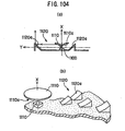
FIG.104 shows the LED light disclosed therein. FIG.104
(a) is a cross sectional view showing the LED light with a light
source centered. FIG.104 (b) is a perspective view showing
part of the LED light. The LED light is composed of: the light
source 1100; a first reflection surface 1110 that is disposed
at a position on the center axis of light source 1100 while
being opposite to the light source 1100 and that has a parabolic
reflection surface 1110a to allow light radiated from the light
source 1100 to be reflected in the Y direction nearly orthogonal
to the center axis X of light source 1100; and a second
reflection surface 1120 that is disposed around the first
reflection surface 1110 and that has a plurality of reflection
facets 1120a to allow light reflected by the first reflection
surface 1110 to be reflected in the direction of center axis
X. In this composition, light to be radiated from the light
source 1100 is reflected in the Y direction by the parabolic
reflection surface 1110a of first reflection surface 1110, and
then the reflected light is reflected in the direction of center
axis X by the reflection facets 1120a of second reflection
surface 1120. Thus, vehicle signaling light with a
predetermined radiation angle can be radiated over a
predetermined area.
-
However, in the LED light, there is a problem that light
directly radiated from the light source 1100 cannot be taken
out in the perpendicular direction because of being blocked
by the first reflection surface 1110 disposed over the light
source 1100 and, therefore, a dark portion is generated at the
center.
-
To solve this problem, International Publication
No.99/09349 discloses an LED light.
-
FIG.105 shows the LED light disclosed therein. FIG.105
(a) is a cross sectional view showing the LED light with a light
source centered. FIG.105 (b) is a cross sectional view cut
along the line K-K in FIG.105 (a). The LED light is composed
of: a light source 1620 that has a light emitting element 1600,
light emitting source, a dome section 1610 and a base section
1610A; a lens element 1740 that has an incident surface 1630,
a first reflection region 1640, a first reflection surface
1640A, a direct transmitting region 1650, a second reflection
region 1660, a radiation surface 1670, an edge 168, and posts
1720, 1730; and an optical element 1750 that pillow lenses 1750A
are arrayed. The second reflection region 1660 of lens element
1740 has pairs of an extraction surface 1660A and a step down
1660B that are formed 360 degrees around the first reflection
region 1640. Further, as shown in FIG.105 (b), the light
source 1620 is composed such that the dome section 1610 is
positioned at the center of first reflection region 1640 by
fitting the posts 1720, 1730 of lens element 1740 into recesses
1620A, 1620B of the base section 1610A.
-
In this composition, light to be radiated from the light
source 1620 is reflected by the first reflection surface 1640A
in a direction orthogonal to the center axis of light source
1620. Then, reflected light is further reflected by the
extraction surface 1660A in the center axis direction to be
radiated as light A from the radiation surface 1670. On the
other hand, light B from the light source 1620 is directly
transmitted though the direct transmitting region 1650 to be
radiated in the center axis direction. Thus, light with an
enlarged radiation area is entered into the optical element
1750.
-
However, in the above LED light, there is a problem that
the entire thickness must be increased since there is provided
the dome section 1610 to converge light radiated from the light
source 1620 to the center axis.
-
Further, it is difficult to perfectly align the center
axis of lens element 1740 with the center axis of light source
1620 in fabrication and, therefore, a deviation in position
may occur and uniformity in brightness is difficult to obtain
over all directions. Namely, the light source 1620 and lens
element 1740 are separately prepared and then aligned with each
other in fabrication. If a precision in alignment of the
center axis of light source 1620 with the first reflection
region 1640 of lens element 1740 lowers, the amount of reflected
light in all reflection directions given by the first
reflection region 1640 becomes uneven and unevenness
(difference) in brightness will occur on the surface of LED
light. Especially in the case of optical system with such a
high light focusing characteristic that most of light radiated
from the light source 1620 is radiated upward, there occurs
a significant difference in brightness due to unevenness in
the light distribution of light source 1620 itself or due to
unevenness in optical characteristics thereof caused by a
deviation in position in a direction perpendicular to the
center axis between the lens element 1740 and the light source
1620. Namely, in the above LED light, since light form the
light emitting element 1600 is radiated being focused by the
dome section 1610, there may occur a significant difference
in the distribution of light to be radiated from the dome
section 1610 even when a slight deviation in position is
generated between the center axis of light source 1600 and the
center axis of dome section 1610. As described above, it has
a potential problem that the structure of light source 1620
itself may cause a difference in light distribution
characteristic. In addition, due to a deviation in position
in mounting the lens element 1740 separately prepared, there
occurs a problem that the amount of reflected light in all
reflection directions given by the first reflection region
1640 becomes uneven.
-
Further, there are problems that the light utilization
efficiency lowers due to sideward light not enabled to be
focused on the center axis by the dome section 1610 and that
the radiation area cannot be therefore enlarged. Namely,
light to be radiated from the light source 1620 in the
horizontal direction (X direction) is reflected by the second
reflection region 1660. Further, light not enabled to be
reflected by neither the first reflection region 1640 nor the
second reflection region 1660 is not radiated in the Z direction.
Thus, the light utilization efficiency lowers.
-
Further, since the light source 1620 and the lens element
1740 are prepared separately, light from the light source 1620
is transmitted through air layer before entering into the
incident surface 1630 of lens element 1740. Therefore, loss
of light is generated in that air layer or at the interface.
If a stain exists at the interface of the light source 1620
and lens element 1740, further loss of light is generated.
Still further, due to the separate preparation, a deviation
in position may occur when being subjected to a physical shock.
Therefore, it is difficult to design an optical system that
the light emitting element and reflection mirror is close to
each other. Further, there are problems that the number of
parts or fabrication steps increases and that variation of
precision in fabrication increases.
-
These problems described above are also included in the
LED light disclosed in Japanese patent application laid-open
No.2001-93312.
-
Accordingly, even when a lamp such as an automobile brake
lamp-integrated tail lamp is manufactured by using such LED
lights, the proper brightness of light source cannot be
utilized due to the above problems. Because of this, the lamp
appears dark as a whole and lacks a degree of freedom in
appearance.
-
An object of the invention is to provide a light emitting
diode and an LED light that have a good appearance based on
the low-profile property of LED, an enlarged radiation area
while using one light emitting element, and an even brightness
in all directions and high external radiation efficiency, and
to provide a high-brightness lamp that is enabled to
efficiently use light radiated from a light source.
-
Another object of the invention is to provide a light
emitting unit that is low-profile, highly efficient and that
can be applied to an irregular shape without reducing the
efficiency and that can be disposed along a slope while having
high external radiation efficiency.
-
A further object of the invention is to provide a lamp
using a light emitting unit that is enabled to radiate light
with an angle widened as much as possible while preventing the
proper brightness of a light source.
-
A still further object of the invention is to provide
a lamp that is low-profile, highly efficient, and that has a
large degree of freedom in appearance and an even brightness
on the entire surface and that offers a natural feel with
glitter.
Disclosure of Invention
-
To solve the abovementioned problems, a light emitting
diode (LED) of the invention comprises:
- a light emitting element mounted on a power source supply
means;
- a sealing means of a transparent material to seal the
light emitting element;
- a reflection surface that is opposite to an emission
surface of the light emitting element and reflects light
emitted from the light emitting element in a direction
orthogonal to the center axis of the light emitting element
or in a direction at a large angle to the center axis; and
- a side radiation surface that sideward radiates light
reflected by the reflection surface in a direction orthogonal
to the center axis of the light emitting element or in a
direction at a large angle to the center axis.
-
-
The LED may have a central radiation surface that is
disposed at the center of the reflection surface and radiates
light emitted from the light emitting element in a direction
nearly parallel to the center axis of the light emitting
element.
-
It is desirable that the central radiation surface has
an area smaller than the emission area of the light emitting
element. For example, when the central radiation surface is
formed circular, it is more desirable that it is 0.1 mm or more
and less than the diagonal length of emission surface of the
light emitting element. This is because, in the case of less
than 0.1 mm, the radiation effect of central radiation surface
cannot be expected so much and, in the case of exceeding the
diagonal length of emission surface, light cannot be
efficiently radiated in the horizontal direction and, when a
reflection mirror is provided around the light emitting
element, the reflection intensity by reflection mirror is
unbalanced to the radiation intensity from central radiation
surface. The central radiation surface may be formed planar,
curved, concave or convex, or into its combination.
-
The side radiation surface may radiate, in addition to
light reflected by the reflection surface, light directly
irradiated from the light emitting element in a direction
orthogonal to the center axis or in a direction at a large angle
to the center axis.
-
The central radiation surface and the reflection surface
may be close to the light emitting element. It is preferable
that the distance between central radiation surface and light
emitting element is, for example, in the range of 0.1 mm to
1.5 mm from the element emission surface. It is more
preferable that, when a wire-bonding type light emitting
element is used, the central radiation surface is formed in
the range of 0.3 mm to 1.0 mm from the element emission surface
in the center axis direction of light emitting element. This
is because, in the case of using a wire-bonding type light
emitting element, the wire is upward drawn out and bent and,
therefore, if bent excessively, its disconnection may be
generated, and because at least a space of 0.3 mm is needed
since the wire is also sealed with the transparent resin. In
the case of exceeding 1.0 mm, as described later in embodiment
1, in the wire-bonding type light emitting element, the
increment in solid angle of the reflection surface decreases
and, therefore, its difference decreases as compared to the
case of not forming the central radiation surface.
-
It is preferable that the outer diameter of the sealing
means of transparent material is 5 to 15 mm. This is because,
in the case of less than 5 mm, the reflection efficiency of
reflection surface cannot be expected sufficiently and, in the
case of exceeding 15 mm, the damage to light emitting element
due to resin stress become significant.
-
Further, to solve the abovementioned problems, a light
emitting diode (LED) of the invention comprises:
- a light emitting element mounted on a power source supply
means; and
- a sealing means of a transparent material to seal the
light emitting element;
wherein the sealing means comprises: a reflection
surface that reflects light emitted from the light emitting
element in a direction orthogonal to the center axis of the
light emitting element or in a direction at a large angle to
the center axis; and a side radiation surface that sideward
radiates light reflected by the reflection surface; and the
reflection surface has a shortest distance from the light
emitting element of less than 1/2 a radius R of the reflection
surface so as to form a proximity optical system.-
-
Further, a light emitting diode (LED) of the invention
comprises:
- a light emitting element mounted on a power source supply
means; and
- a sealing means of a transparent material to seal the
light emitting element;
wherein the sealing means comprises: a reflection
surface that reflects light emitted from the light emitting
element in a direction orthogonal to the center axis of the
light emitting element or in a direction at a large angle to
the center axis; and a side radiation surface that sideward
radiates light reflected by the reflection surface; and the
reflection surface is formed such that its radius R is greater
than a height H from the emission surface of the light emitting
element to an edge of the reflection surface in the center axis
direction of the light emitting element so as to form a
proximity optical system.-
-
It is desirable that, in the LED, the light emitting
element has a radiation intensity I () represented by:
I()=k · cos + (1-k) · sin at an emission angle of emitted
light to the center axis direction, where k is a constant to
be determined by a radiation intensity according to the
emission angle of the light emitting element, and k≦0.8 is
satisfied.
-
It is preferable that, in the LED, the light emitting
element comprises a transparent substrate to have a light
transmitting property to light emitted therefrom.
-
It is desirable that, in the LED, the sealing means
comprises a light diffusing material to cover the light
emitting element.
-
In the LED, the light diffusing material may be a
phosphor.
-
Further, to solve the abovementioned problems, a light
emitting diode (LED) of the invention comprises:
- a light emitting element that is mounted on a power source
supply means and sealed with a sealing member of a transparent
material; and
- the sealing member that comprises a reflection surface
and a side reflection surface formed thereon, the reflection
surface reflecting light radiated from an emission surface of
the light emitting element and the side radiation surface
radiating reflected light from the reflection surface and
direct light form the light emitting element;
wherein the reflection surface has a solid angle of 2
π{1-cosc} or greater to the light emitting element, where
c is a critical angle of the transparent material, and the
side radiation surface is formed such that an incident angle
of reflected light from the reflection surface and an incident
angle of direct light from the light emitting element are
smaller than c so as to externally radiate light emitted from
the light emitting element.-
-
The reflection surface may have a shape to be formed by
rotating, around the center axis of the light emitting element,
part of a line represented by Z=f (X) in a plane formed between
the center axis (Z-axis) of the light emitting element and an
X-axis orthogonal to the Z-axis, and the Z=f(X) satisfies
{d2f(X)/dX2}<0. If the Z=f(X) satisfies {d2f(X)/dX2}<0, even
when a large solid angle to the light emitting element is taken
in the case of the reflection surface having the same diameter,
then an incident angle to the side radiation surface can be
small.
-
The reflection surface may have a shape to be formed by
rotating, around the center axis of the light emitting element,
part of ellipse, parabola or hyperbola with a focal point at
the light emitting element or its vicinity. These are typical
forms, practically available, of curves represented by
{d2f(X)/dX2}<0.
-
The side radiation surface may have a slope to be inclined
to the light emitting element.
-
The side radiation surface may compose part of a
spherical surface centered at the light emitting element.
-
Further, to solve the abovementioned problems, a light
emitting diode (LED) of the invention comprises:
- the lead frame that is protruded out of the transparent
resin while being bent under its mount surface from the vicinity
of a mount position of the light emitting element so as to reduce
part of the lead frame sealed with the transparent resin as
much as possible.
-
-
The LED may comprise the lead frame that comprises part
sealed with the transparent resin that has a wide area
sufficient to widely conduct and disperse heat generated from
the light emitting element.
The lead frame may be of a material with a high thermal
conductivity. It is desirable that it is of a conductive
material with a thermal conductivity of 300W/m · k or more.
-
Further, a light emitting diode of the invention may
comprise:
- a light emitting element to emit light;
- a lead frame to supply electric power to the light
emitting element mounted thereon; and
- a transparent resin to seal the light emitting element
and the lead frame;
wherein the transparent resin comprises: a first
transparent resin to seal the light emitting element and part
of the lead frame; and a second transparent resin disposed in
contact with and around the side of the first transparent resin.-
-
Further, to solve the abovementioned problems, a light
emitting diode (LED) of the invention comprises:
- an light emitting section that comprises a
two-dimensional direction reflection surface to reflect light
emitted from a light emitting element embedded in a transparent
material at least in a two-dimensional direction; and
- a reflector section that is optically connected at least
around in the two-dimensional direction of the light emitting
section and comprises a reflection surface formed extending
from the two-dimensional direction reflection surface.
-
-
The reflector section may be formed low-profile and
additionally reflect light reaching a surface opposite to the
reflection surface of light radiated from the light emitting
section.
-
The reflector may comprise a stepwise reflection surface
that is opposite to the reflection surface and, in a direction
perpendicular to the two-dimensional direction, reflects
light being reflected by the two-dimensional direction
reflection surface and the reflection surface in the
two-dimensional direction.
-
The two-dimensional direction reflection surface of the
light emitting section may have a shape to be formed by rotating,
around a perpendicular axis passing through the center of an
emission surface of the light emitting element, part of ellipse,
parabola, hyperbola or its approximated curve with a focal
point at the light emitting element or its vicinity.
-
A light emitting diode of the invention may comprise:
- a light source section that comprises a circular cone
portion that is opposite to an emission surface of a light
emitting element embedded and is formed protruding outside;
and
- a reflection section that comprises a two-dimensional
direction reflection surface that is connected at least to the
circular cone portion and reflects light radiated from the
light source section at least in a two-dimensional plane
direction.
-
-
Further, to solve the abovementioned problems, an LED
light of the invention comprises:
- an LED; and
- a reflection mirror disposed around the LED;
wherein the LED comprises: a light emitting element
mounted on a power source supply means; a sealing means of a
transparent material to seal the light emitting element; a
reflection surface that is opposite to an emission surface of
the light emitting element and reflects light emitted from the
light emitting element in a direction orthogonal to the center
axis of the light emitting element or in a direction at a large
angle to the center axis; and a side radiation surface that
sideward radiates light reflected by the reflection surface
in a direction orthogonal to the center axis of the light
emitting element or in a direction at a large angle to the center
axis.-
-
It is desirable that the LED further comprises a central
radiation surface that is disposed at the center of the
reflection surface and radiates light emitted from the light
emitting element in a direction nearly parallel to the center
axis of the light emitting element.
-
An LED light of the invention may comprise:
- an LED that comprises: a light emitting element mounted
on a power source supply means; and a sealing means of a
transparent material to seal the light emitting element;
wherein the sealing means comprises: a reflection surface that
reflects light emitted from the light emitting element in a
direction orthogonal to the center axis of the light emitting
element or in a direction at a large angle to the center axis;
and a side radiation surface that sideward radiates light
reflected by the reflection surface; and the reflection
surface has a shortest distance from the light emitting element
of less than 1/2 a radius R of the reflection surface so as
to form a proximity optical system; and
- a reflection mirror that reflects light radiated from
the LED.
-
-
The light emitting element may have a radiation intensity
I() represented by: I() =k · cos + (1-k) · sin at an emission
angle of emitted light to the center axis direction, where
k is a constant to be determined by a radiation intensity
according to the emission angle of the light emitting
element, and k≦0.8 is satisfied.
-
An LED light of the invention may comprise:
- an LED that comprises: a light emitting element that is
mounted on a power source supply means and sealed with a sealing
member of a transparent material; and the sealing member that
comprises a reflection surface and a side reflection surface
formed thereon, the reflection surface reflecting light
radiated from an emission surface of the light emitting element
and the side radiation surface radiating reflected light from
the reflection surface and direct light form the light emitting
element; wherein the reflection surface has a solid angle of
2π{1-cos c} or greater to the light emitting element, where
c is a critical angle of the transparent material, and the
side radiation surface is formed such that an incident angle
of reflected light from the reflection surface and an incident
angle of direct light from the light emitting element are
smaller than c so as to externally radiate light emitted from
the light emitting element; and
- a reflection mirror that reflects light radiated from
the LED.
-
-
An LED light of the invention may comprise:
- an LED that comprises: a light emitting element to emit
light; a lead frame to supply electric power to the light
emitting element mounted thereon; and a transparent resin to
seal the light emitting element and the lead frame; wherein
the lead frame is protruded out of the transparent resin while
being bent under its mount surface from the vicinity of a mount
position of the light emitting element; and
- a reflection mirror that reflects light radiated from
the LED.
-
-
An LED light of the invention may comprise:
- an LED that comprises: a light emitting element to emit
light; a lead frame to supply electric power to the light
emitting element mounted thereon; and a transparent resin to
seal the light emitting element and the lead frame; wherein
the lead frame comprises part sealed with the transparent resin
that has a wide area sufficient to widely conduct and disperse
heat generated from the light emitting element; and
- a reflection mirror that reflects light radiated from
the LED.
-
-
An LED light of the invention may comprise:
- a light emitting element;
- a first reflection mirror that is formed on the light
emitting element and reflects light emitted from the light
emitting element in the side direction; and
- a second reflection mirror that upward reflects light
from the first reflection mirror.
-
-
A third reflection mirror may be disposed inside the
second reflection mirror and upward reflects light sideward
emitted from the light emitting element.
-
The first reflection mirror and the second reflection
mirror may be formed into one optical member.
-
The second reflection mirror may be in the shape of a
polygon or its similar form when viewed from upward.
-
The light emitting element may be mounted on a circuit
board on a metal plate.
-
Further, to solve the abovementioned problems, a light
emitting unit of the invention comprises:
- a light source that comprises: a light emitting element
mounted on a power source supply means; a sealing means of a
transparent material to seal the light emitting element; a
first reflection surface that is opposite to an emission
surface of the light emitting element and reflects light
emitted from the light emitting element in a direction
orthogonal to the center axis of the light emitting element
or in a direction at a large angle to the center axis; and a
side radiation surface that sideward radiates light reflected
by the first reflection surface in a direction orthogonal to
the center axis of the light emitting element or in a direction
at a large angle to the center axis; and
- a reflector that comprises a plurality of second
reflection surfaces to reflect the light radiated from the side
radiation surface in a predetermined radiation direction.
-
-
It is preferable that, in the light emitting unit, the
light source further comprises a central radiation surface
that is disposed at the center of the first reflection surface
and radiates light emitted from the light emitting element in
a direction nearly parallel to the center axis of the light
emitting element.
-
It is preferable that, in the light emitting unit, the
first reflection surface is formed close to the light emitting
unit so as to increase a light receiving angle (solid angle)
of the upper reflection surface.
-
It is preferable that, in the light emitting unit, the
light source is displaced from the center and the position of
optical control surfaces neighboring in the circumference
direction is different from each other in the radius direction.
-
In the light emitting unit, the reflector may reflect
the light, as the predetermined radiation direction, in a
direction with a predetermined inclination to the center axis
of the light emitting element by the plurality of second
reflection surfaces.
-
In the light emitting unit, the reflector may be mounted
on an inclined section.
-
In the light emitting unit, the plurality of second
reflection surfaces each may have an optical control surface
that its angle and direction are set to allow reflected light
to be reflected in a same direction.
-
Further, to solve the abovementioned problems, a lamp
of the invention comprises:
- a plurality of light emitting units each of which
comprises: a light source that comprises an optical system to
radiate light emitted from a light emitting element in a
direction orthogonal to the center axis of the light emitting
element or in a direction at a large angle to the center axis;
and a reflector that comprises a plurality of second reflection
surfaces to, in a predetermined direction, reflect the light
radiated from the light source in the direction orthogonal to
the center axis of the light emitting element or in the
direction at the large angle to the center axis;
wherein the plurality of light emitting units are
disposed in a predetermined arrangement.-
-
In the lamp, the light source may have a lead frame fixed
on a board disposed on the back side of a housing, and its fixing
position corresponds to a penetration hole of the reflection
mirror.
-
In the lamp, the board may be, at the fixing position,
provided with a concave member into which the lead frame is
inserted.
-
In the lamp, the light source may comprise: a light
emitting element mounted on a power source supply means; a
sealing means of a transparent material to seal the light
emitting element; a first reflection surface that is opposite
to an emission surface of the light emitting element and
reflects light emitted from the light emitting element in a
direction orthogonal to the center axis of the light emitting
element or in a direction at a large angle to the center axis;
and a side radiation surface that sideward radiates light
reflected by the first reflection surface in a direction
orthogonal to the center axis of the light emitting element
or in a direction at a large angle to the center axis.
-
In the lamp, the light source may comprise a plurality
of LED's that are arranged radially such that an intersection
point of the center axes of the plurality of LED's is a point
on a same plane.
-
In the lamp, the plurality of light emitting units may
be disposed such that part of the reflector of the neighboring
light emitting units is overlapped.
-
In the lamp, the plurality of light emitting units may
include a plurality of light emitting units that are arranged
at multiple stages or in multiple rows, and the light emitting
units at each stage include a plurality of light emitting units
arranged linearly.
-
In the lamp, the plurality of light emitting units may
be arranged through a partition plate to separate the plurality
of light emitting units arranged linearly.
-
In the lamp, the plurality of light emitting units may
have a light reflection finish on at least part of the
circumference of the light emitting unit or the partition
plate.
-
In the lamp, the plurality of light emitting units may
be disposed such that the neighboring light emitting units are
arranged at different stages in the center axis direction.
-
In the lamp, the plurality of light emitting units may
be composed such that a plurality of reflection surfaces are
concentric disposed around the light source.
-
In the lamp, the plurality of reflection surfaces may
be formed nearly planar.
-
Herein, "angle" means an angle of the light source to
the light radiation surface and "direction" means an angle of
the light source to the light radiation direction.
Brief Description of Drawings
-
- FIG.1 is a cross sectional view showing a light emitting
diode in embodiment 1A of the invention.
- FIG.2 is an enlarged cross sectional view showing part
of the light emitting diode in embodiment 1A of the invention.
- FIG.3 is graphs showing the relationship between a
distance h from the upper surface of a light emitting element
to a central radiation surface and an increment of solid angle
in the light emitting diode shown in FIG. 2, wherein (a) is the
case of a diameter in transparent resin of 5 mm, (b) of 7.5
mm and (c) of 15 mm.
- FIG.4 is cross sectional views showing shape examples
of the central radiation surface of the light emitting diode
in embodiment 1A of the invention, wherein (a) is planar, (b)
is curved only at the boundary of central radiation surface
and upper reflection surface, (c) is curved on the entire
central radiation surface, (d) is concaved and (e) is convexed.
- FIG.5 is a graph illustrating another example of upper
reflection surface of the light emitting diode in embodiment
1A of the invention.
- FIG.6 is a cross sectional view showing another example
of the light emitting diode in embodiment 1A of the invention.
- FIG.7 is a cross sectional view showing another example
of the light emitting diode in embodiment 1A of the invention.
- FIG.8 is a cross sectional view showing another example
of the light emitting diode in embodiment 1A of the invention.
- FIG.9 is a cross sectional view showing a method
(transfer molding) of making the light emitting diode in
embodiment 1A of the invention.
- FIG.10 is a cross sectional view showing a method
(casting mold) of making the light emitting diode in embodiment
1A of the invention.
- FIG.11 (a) is a plain view showing an LED light in
embodiment 1B of the invention, (b) is a cross sectional view
cut along the line A-A in (a), and (c) is an enlarged cross
sectional view showing part P in (b).
- FIG. 12 is a cross sectional view showing an LED as a light
source of the LED light in embodiment 1B of the invention.
- FIG.13 is a plain view showing an integrated LED light
to cover a predetermined area, wherein a plurality of the LED
lights in embodiment 1B of the invention are cut into
rectangular form.
- FIG.14 is a cross sectional view showing a first
modification of LED as a light source of the LED light in
embodiment 1B of the invention.
- FIG.15 is a cross sectional view showing a second
modification of LED as a light source of the LED light in
embodiment 1B of the invention.
- FIG.16 is a cross sectional view showing a third
modification of LED as a light source of the LED light in
embodiment 1B of the invention.
- FIG.17 is a cross sectional view showing a fourth
modification of LED as a light source of the LED light in
embodiment 1B of the invention.
- FIG.18 (a) is a plain view showing a fifth modification
of the LED light in embodiment 1B of the invention, (b) is a
cross sectional view cut along the line B-B in (a), (c) is a
cross sectional view cut along the line C-C in (a), and (d)
is a cross sectional view cut along the line D-D in (a).
- FIG.19 (a) is a plain view showing a sixth modification
of the LED light in embodiment 1B of the invention, (b) is a
cross sectional view cut along the line E-E in (a), and (c)
is a cross sectional view cut along the line F-F in (a).
- FIG.20 is a cross sectional view showing an LED used for
an LED light in embodiment 1C of the invention.
- FIG.21 is a cross sectional view showing an LED light
in embodiment 1D of the invention.
- FIG.22 is a cross sectional view showing an LED light
in embodiment 1E of the invention.
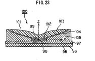
- FIG.23 is a cross sectional view showing an LED light
in embodiment 1F of the invention.
- FIG.24 (a) is a plain view showing an LED light in
embodiment 1G of the invention, and (b) is a cross sectional
view cut along the line G-G in (a).
- FIG.25 (a) is a plain view showing an LED light using
an LED in embodiment 2A of the invention, (b) is a cross
sectional view cut along the line A-A in (a), and (c) is an
enlarged cross sectional view showing part P of (b).
- FIG. 26 (a) is a cross sectional view showing an LED used
for the LED light in embodiment 2A of the invention, (b) is
a plain view thereof, and (c) is a side view showing the size
of LED.
- FIG.27 is a side view showing a light emitting element
in embodiment 2A of the invention.
- FIG.28 is an illustration showing light radiated from
an upper surface and a side surface of the light emitting
element in embodiment 2A of the invention.
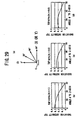
- FIG.29 shows light distribution characteristic curves
in embodiment 2A of the invention, wherein (a) is an
illustration showing an angle to Z-axis of light emitting
element, (b) is a characteristic diagram showing a change in
radiation intensity in case of k=1, (c) is a characteristic
diagram showing a change in radiation intensity in case of k=0. 8,
and (d) is a characteristic diagram showing a change in
radiation intensity in case of k=0.6.
- FIG.30 is a graph showing a relationship between
effective radiation efficiency ratio and a deviation in X-axis
direction in embodiment 2A of the invention.
- FIG. 31 (a) and (b) are illustrations showing observation
conditions of light amount radiated from LED.
- FIG.32 shows a deviation in total light amount in
effective radiation range of LED in embodiment 2A of the
invention, wherein (a) is a characteristic diagram showing a
deviation in total light amount in effective radiation range
of LED using a light emitting element with a top light
distribution characteristic of 100%, and (b) is a
characteristic diagram showing a deviation in total light
amount in effective radiation range of LED using a light
emitting element with a top light distribution characteristic
of 80%.
- FIG.33 (a) is a plain view showing an LED light using
an LED in embodiment 2B of the invention, and (b) is a cross
sectional view showing the vicinity of a light emitting element
in (a).
- FIG.34 (a) is a characteristic diagram showing a
deviation in total light amount in effective radiation range
of LED using a light emitting element with a top light
distribution characteristic of 60% (k=0.6) in embodiment 2B
of the invention.
- FIG.35 (a) is a plain view showing an LED light using
an LED in embodiment 2C of the invention, and (b) is a cross
sectional view showing the vicinity of a light emitting element
in (a).
- FIG.36 is a cross sectional view showing an LED light
using an LED in embodiment 2D of the invention.
- FIG.37 shows an LED in embodiment 3A of the invention,
wherein (a) is a cross sectional view thereof, and (b) is a
plain view thereof.
- FIG. 38 is a graph showing a relationship between incident
angle and transmittance in LED.
- FIG. 39 is a cross sectional view showing a light emitting
element used for the LED in embodiment 3A of the invention.
- FIG.40 (a), (b) and (c) are characteristic diagrams
showing a light intensity distribution, a light flux
distribution, and a light flux integration in a standard light
emitting element (in case of 20 mil and 14 mil).
- FIG.41 is a cross sectional view showing another
reflection surface formed on the LED in embodiment 3A of the
invention.
- FIG.42 (a) is a plain view showing a first modification
of the LED in embodiment 3A of the invention, and (b) is a cross
sectional view thereof.
- FIG.43 is a plain view showing a second modification of
the LED in embodiment 3A of the invention.
- FIG.44 is a plain view showing a third modification of
the LED in embodiment 3A of the invention.
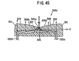
- FIG.45 is a plain view showing a fourth modification of
the LED in embodiment 3A of the invention.
- FIG.46 is a plain view showing a seventh modification
of the LED in embodiment 3A of the invention.
- FIG.47 (a) is a plain view showing an LED light using
an LED in embodiment 3B of the invention, (b) is a cross
sectional view cut along the line A-A in (a), and (c) is an
enlarged cross sectional view showing part P in (b).
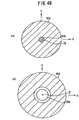
- FIG.48 shows a dimensional relationship between LED and
second reflection mirror in an LED light using the LED in
embodiment 3B of the invention, wherein (a) is the case of using
LED with a small diameter and (b) is the case of using LED with
a large diameter.
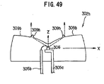
- FIG.49 is a cross sectional view showing an LED used for
a first modification of the LED light in embodiment 3B of the
invention.
- FIG.50 is a cross sectional view showing a second
modification of the LED light in embodiment 3B of the invention.
- FIG.51 is a diagram showing a light distribution
characteristic of LED used for the second modification of LED
light.
- FIG.52 (a) is a plain view showing an LED light using
an LED in embodiment 4A of the invention, (b) is a cross
sectional view cut along the line A-A in (a), and (c) is an
enlarged cross sectional view showing part P in (b).
- FIG.53 is a cross sectional view showing the LED as a
light source of the LED light in embodiment 4A of the invention.
- FIG.54 is a plain view showing the LED in embodiment 4A
of the invention.
- FIG. 55 is a cross sectional view showing a light emitting
element used for the LED in embodiment 4A of the invention.
- FIG.56 is a cross sectional view showing the LED with
lead frames projecting in horizontal direction.
- FIG.57 (a) is a plain view showing the LED with lead
frames of wide area, (b) is a cross sectional view of (a) , and
(c) is a cross sectional view in the case of having fins in
(b).
- FIG. 58 is a cross sectional view showing an LED as a light
source of an LED light in embodiment 5A of the invention.
- FIG. 59 is a plain view showing the LED in embodiment 5A
of the invention.
- FIG.60 is a cross sectional view showing a modification
of LED as a light source of the LED light in embodiment 5A of
the invention.
- FIG.61 (a) is a plain view showing an LED in embodiment
6A of the invention, and (b) is a cross sectional view thereof.
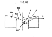
- FIG.62 is an illustration showing a two-dimensional
radiation characteristic of the LED in embodiment 6A of the
invention.
- FIG.63 is a cross sectional view showing a lamp using
the LED in embodiment 6A of the invention.
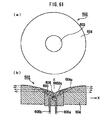
- FIG.64 is a cross sectional view showing an LED in
embodiment 6B of the invention.
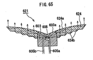
- FIG.65 is a cross sectional view showing an LED in
embodiment 6C of the invention.
- FIG.66 (a) is a plain view showing an LED in embodiment
6D of the invention, and (b) is a cross sectional view thereof.
- FIG.67 is a cross sectional view showing an LED in
embodiment 6E of the invention.
- FIG.68 is a plain view showing a light emitting unit in
embodiment 7A of the invention.
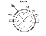
- FIG.69 is a plain view showing an LED as a light source
of the light emitting unit in embodiment 7A of the invention.
- FIG.70 is a cross sectional view showing the LED as a
light source of the light emitting unit in embodiment 7A of
the invention.
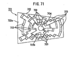
- FIG.71 is a plain view showing a light emitting unit in
embodiment 7B of the invention.
- FIG.72 is a plain view showing a light emitting unit in
embodiment 7C of the invention and a distribution of light
emitting points in the light emitting unit.
- FIG.73 is a cross sectional view showing the light
emitting unit in embodiment 7C to be cut along the line A-A
in FIG.72.
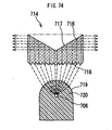
- FIG.74 is a cross sectional view showing a light source
of a light emitting unit in embodiment 7D of the invention.
- FIG.75 is a cross sectional view showing a light source
of a light emitting unit in embodiment 7E of the invention.
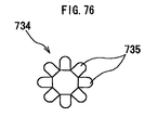
- FIG.76 is a plain view showing a light source of a light
emitting unit in embodiment 7F of the invention.
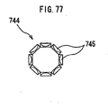
- FIG.77 is a plain view showing a light source of a light
emitting unit in embodiment 7G of the invention.
- FIG.78 is a perspective view showing a lamp in embodiment
7H of the invention.
- FIG.79 is an enlarged perspective view showing part of
a reflection surface of a light emitting unit in embodiment
71 of the invention.
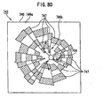
- FIG.80 is a plain view showing the light emitting unit
in embodiment 7I of the invention.
- FIG. 81 is a cross sectional view showing a light emitting
unit in embodiment 7J of the invention.
- FIG.82 (a) is a plain view showing an LED used as a light
source of the light emitting unit in embodiment 7J of the
invention, and (b) is a cross sectional view thereof.
- FIG.83 is a cross sectional view showing the light
emitting unit in embodiment 7J of the invention to be attached
to a car body.
- FIG. 84 is a cross sectional view showing a light emitting
unit in embodiment 7K of the invention.
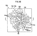
- FIG.85 is a plain view showing the light emitting unit
in embodiment 7L of the invention.
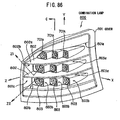
- FIG.86 is a perspective view showing an automobile
combination lamp in embodiment 7M of the invention.
- FIG.87 is a cross sectional view cut along the line C-C
in FIG.86.
- FIG.88 is a perspective view showing an LED mounting
board of the combination lamp in FIG.87.
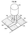
- FIG.89 is an enlarged perspective view showing an LED
mounting part of the LED mounting board in FIG.88.
- FIG.90 is a front view showing an automobile combination
lamp in embodiment 7N of the invention.
- FIG.91 is a cross sectional view cut along the line J-J
in FIG.90.
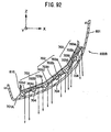
- FIG.92 is a cross sectional view showing an automobile
combination lamp in embodiment 7P of the invention.
- FIG.93 (a) is a plain view showing a lamp in embodiment
8A of the invention, and (b) is a cross sectional view thereof.
- FIG.94 (a) is a cross sectional view cut along the line
A-A to show a segment of the lamp in embodiment 8A of the
invention, and (b) is a cross sectional view cut along the line
B-B.
- FIG.95 (a) is a cross sectional view cut along the line
A-A to show a segment of a modification of the lamp in embodiment
8A of the invention, and (b) is a cross sectional view cut along
the line B-B.
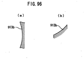
- FIG.96 (a) is a cross sectional view cut along the line
A-A to show a segment of another modification of the lamp in
embodiment 8A of the invention, and (b) is a cross sectional
view cut along the line B-B.
- FIG.97 is a plain view showing a lamp in embodiment 8B
of the invention.
- FIG.98 is a plain view showing a lamp in embodiment 8C
of the invention.
- FIG.99 is a plain view showing a lamp in embodiment 8D
of the invention.
- FIG.100 is a cross sectional view showing a lamp in
embodiment 8E of the invention.
- FIG.101 (a) is a plain view showing a radiation light
source used for a lamp in embodiment 8F of the invention, (b)
is a plain view showing a lens type LED to compose the radiation
light source, (c) is a side view thereof, and (d) is a front
view thereof.
- FIG.102 (a) is a plain view showing a radiation light
source used for a lamp in embodiment 8G of the invention, (b)
is a plain view showing a reflection type LED to compose the
radiation light source, and (c) is a cross sectional view
thereof.
- FIG. 103 is a cross sectional view showing an example of
the conventional LED light.
- FIG.104 shows another example of the conventional LED
light, wherein (a) is a cross sectional view showing the LED
light with a light source centered, and (b) is a perspective
view showing part of the LED light.
- FIG.105 shows another example of the conventional LED
light, wherein (a) is a cross sectional view showing the LED
light with a light source centered, and (b) is a cross sectional
view cut along the line K-K in (a).
-
Best Modes for Carrying Out the Invention
-
The embodiments of the invention will be explained below
with reference to the drawings.
[Embodiment 1A]
-
At first, a light emitting diode in embodiment 1A of the
invention will be explained with reference to FIG.1 and FIG.2.
As shown in FIG.1, the light emitting diode 10 has a light
emitting element 1 that has dimensions of 400x400 µm and is
mounted through Ag paste (not shown) on a lead frame 2a. The
light emitting element 1 has an electrode, which has a diameter
of 0.1 mm and is formed on the center of emission surface, and
a gold wire ball (not shown) formed thereon that are
electrically connected through a wire 3 with a diameter of 30
µm to a lead 2b with an opposite polarity. These are sealed
with transparent resin 4 and the optical surface is molded.
-
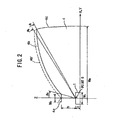
As shown in FIG.2, the optical surface is composed of
a central radiation surface 4a, an upper reflection surface
4b and a side radiation surface 4c. The central radiation
surface 4a is h=0. 5 mm above the upper surface of light emitting
element 1 and is in the shape of a cylinder with a diameter
of Wc=0.3 mm. The upper reflection surface 4b is formed by,
around a z-axis, rotating a parabola that has a focal point
at the center of upper surface of light emitting element 1,
passing through the end of central radiation surface 4a, and
having a symmetry axis perpendicular to the z-axis. The side
radiation surface 4c is formed as a cylindrical surface that
is nearly perpendicular to the z-axis and is slightly tapered
to facilitate the release from a die. The transparent resin
4 composed of the central radiation surface 4a, upper
reflection surface 4b and side radiation surface 4c has an outer
diameter of Wm=7.5 mm.
-
In order to have a larger sold angle when the transparent
resin 4 is set to be a predetermined outer diameter, the upper
reflection surface may have a shape to be formed by rotating
a parabola with the same focal position and a smaller homothetic
ratio (for example, 4b' to 4b). However, in the case of a wire
bonding type light emitting element, a wire space is needed
over the light emitting element 1 as shown in FIG.1. Namely,
the light emitting element 1 has an electrode (n-electrode or
p-electrode) on its upper surface and the wire 3 is bonded
thereto. A space of at least 0.3 mm (0.2 mm for wire and 0.1
mm for seal) is required since the wire 3 to be drawn upward
and bent in installation may be broken when being extremely
bent and it has to be sealed with transparent resin. Therefore,
the optical surface is provided with the upper reflection
surface 4b with a homothetic ratio smaller than a virtual upper
reflection surface 4b' indicated by a dotted curve and with
the central radiation surface 4a.
-
Due to the optical surface thus composed, light heading
to the Z-axis direction can be radiated from the center of LED
package and the reflection efficiency in a direction
perpendicular to the Z-axis can be enhanced. Namely, in FIG.2,
provided that the center of emission surface of light emitting
element 1 is point 0 (zero), an angle to the Z-axis of a
direction from the point 0 edge to the edge of upper reflection
surface is 0=60 degrees in the case of dotted curve 4b' and
1=65 degrees in the case of solid curve 4b. These angles
correspond to, as solid angle, A0=3.1 strad and A1=3.6 strad
to the point 0 (in both cases, the upper reflection surface
has a shape to be formed by rotating, around the Z-axis, a
parabola with a symmetry axis perpendicular to the Z-axis).
On the other hand, an angle 2 to the Z-axis of a direction
from the point 0 to the edge of central radiation surface is
17 degrees and a solid angle to the point 0 is A2=0.25 strad.
Namely, by providing the optical surface indicated by the solid
curve, although at part of the central radiation surface the
solid angle is decreased by A2=0.25 strad since reflection to
a direction nearly perpendicular to the Z-axis is not obtained,
an increment of solid angle becomes A1-A0=0.5 by changing 4b'
into 4b. Thus, an increment of solid angle is eventually
(A1-A0)-A2=0.25 when the decrement is subtracted. A
solid-angle increment ratio of upper reflection surface to
light source is 0.25/π, i.e., increased by about 10 %.
Accordingly, the radiation efficiency to a direction
perpendicular to the Z-axis can be enhanced.
-
Although in embodiment 1A the light emitting diode 10
is exemplified that the central radiation surface with a
diameter of 0.3 mm is provided the light emitting element 1
of 400 µm square, the other dimensions may be used other than
the above. However, if the central radiation surface 4a is
extremely expanded, more light will be radiated from the upper
surface and the radiation efficiency to a direction
perpendicular to the Z-axis will lower. Thereby, the original
concept will be spoiled. Therefore, it is desired that the
central radiation surface 4a is limited to about the dimensions
of emission surface of light emitting element or smaller.
Further, although in embodiment 1A the distance h between the
upper emission surface of light emitting element 1 and the
central radiation surface is 0.5 mm and the diameter of
transparent resin 4 is 7.5 mm, suitable values other than the
above may be used in the range the effect can be obtained.
-
FIG.3 (a), (b) and (c) show, as a function of h, a
solid-angle increment of upper reflection surface to point 0
in the case of forming a central radiation surface (4a and 4b)
in comparison with the case of not forming a central radiation
surface (4b' in FIG.2) while setting the diameter of
transparent resin to be 5mm, 7.5 mm and 15 mm, respectively.
Referring to FIG.3 (b), in the case of transparent resin with
a diameter of 7.5 mm, the solid-angle increment can be maximum
at h=0.6 mm as compared to the case of not forming the central
radiation surface. If h increases greater than this, a
difference to the case of not forming the central radiation
surface decreases and the solid-angle increment of upper
reflection surface lowers. On the other hand, if h decreases,
the solid-angle increment of upper reflection surface lowers
since a solid angle occupied by the central radiation surface
increases. Even when the diameter of transparent resin is
changed, the same tendency is observed. Such a tendency is
significant in the case of transparent resin with a small
diameter rather than in the case of transparent resin with a
large diameter. However, if the diameter is less than 15 mm,
the advantageous effect in solid-angle increment can be
obtained by providing the central radiation surface. In view
of the above results, it is desirable to have h=0.3 to 1.0 mm
and a diameter of transparent resin of 5 to 15 mm.
-
In FIG.2 and FIG.3, when the central radiation surface
4a is closed to the emission surface of light emitting element
1 like the case of transparent resin with a diameter of 15 mm
and h=0.3 mm, the edge angle (2) of central radiation surface
4a and its solid angle (A2) are increased theoretically.
Therefore, the solid-angle increment (A1-A0)-A2) of upper
reflection surface 4b to point 0 in the case of forming a central
radiation surface in comparison with the case of not forming
a central radiation surface becomes negative as shown in FIG. 3
(c) . However, in fact, since the light emitting element under
the central radiation surface 4a is provided with the electrode
with a diameter of 0.1 mm formed on the center of its emission
surface and with the gold wire ball which are all non-emission
parts, the amount of light to be externally radiated from the
central radiation surface does not increase. Therefore, the
influence of negative solid-angle increment caused by A2 is
exactly weak and the radiation efficiency to a direction nearly
perpendicular to the Z-axis can be enhanced due to an increment
(A1-A0).
-
The central radiation surface 4a is not limited to planar
as shown in FIG.4 (a) and may be curved only at the boundary
of central radiation surface 4a and upper reflection surface
4b as shown in FIG.4 (b), curved over the entire central
radiation surface 4a as shown in FIG.4 (c), concave as shown
in FIG.(d), or convex as shown in FIG.4 (d).
-
The upper reflection surface 4b may have a shape to be
formed not only by rotating a parabola with a focal point at
the center of upper surface of light emitting element and with
a symmetry axis on the X-axis but also by rotating a parabola
that has a symmetry axis in a direction inclined from the X-axis
as shown in FIG.5. Further, it may have a shape to be formed
by rotating an ellipse with long focus or hyperbola or the like
other than parabolas.
-
The light emitting element may be provided with the
electrode formed at the periphery of upper surface other than
at the center of upper surface. In this case, the limitation
of dimension h as described above does not occur in view of
wire space. However, if disposed too close, the solid angle
(to he light emitting element) of the central radiation surface
4a becomes significantly large at the upper reflection surface
4b. In the resin sealing, if the gap is narrow, the resin may
be not filled therein and the light emitting element may be
subjected to an unnatural stress even after the sealing.
Therefore, it is desirable that a predetermined space is
provided between the upper emission surface of light emitting
element 1 and the central radiation surface.
-
The package form is not limited to that shown in FIG.1
and may be such that copper-foil patterns 5a, 5b are formed
on a metal board 7 through an insulation layer 6 and the light
emitting element 1 is formed thereon as shown in FIG.6 or such
that leads 8a, 8b are drawn below as shown in FIG.7.
-
The light emitting element may be coated with phosphor.
In this case, as shown in FIG.8, a light source 9 can be such
that the light emitting element 1 is sealed with a coat
including phosphor 12.
-
The light emitting diode 10 in embodiment 1A can be
fabricated by using, e.g., the transfer molding. The transfer
molding will be explained below referring to FIG.9. At first,
the light emitting element 1 is face-up bonded to the lead frame
2a being formed by pressing. Then, an A1 bonding pad of the
light emitting element 1 is electrically connected through a
wire 3 to the lead frame 2b. Then, the lead frame 2a, 2b with
the light emitting element 1 mounted is positioned on a die
20B, and sandwiched by a descending die 20A to keep the position
of lead frames and die. Then, transparent epoxy 4 including
a release agent is injected into the die. Then, the
transparent epoxy 4 is cured under the conditions of 160°C
and 5 min. Then, the dies 20A, 20B are separated vertically
and the light emitting diode 10 with transparent epoxy cured
is taken out. In thus fabricating the light emitting diode
10 by the transfer molding, the transparent resin 4 is injected
into interiors 20C, 20D of the die while sandwiching the lead
frames 2a, 2b. Therefore, the positioning between the light
emitting element 1 and optical surface can be performed at a
high precision of ±0.1 mm. Thereby, dispersion in light
distribution characteristic due to an individual difference
of the light emitting diode 10 using the proximity optical
system can be prevented.
-
The light emitting diode 10 can be also fabricated by
the casting mold. The casting mold will be explained below
referring to FIG.10. At first, lead frames 21a, 21b are
punched out by pressing. At that time, the lead frames 21a,
21b are kept connected with a lead at its multiple ends without
being separated. Then, the lead-connected ends are secured
by a supporting member. Then, the light emitting element 1
is face-up bonded to the tip of lead frame 21b. Then, an A1
bonding pad of the light emitting element 1 is electrically
connected through a wire 3 to the lead frame 21a. Then, the
lead frames 21a, 21b are moved above a casting 20F for molding.
Then, resin 4 is injected into the casting 20F. Then, the lead
frames 21a, 21b are soaked in the casting 20F with resin 4
injected. Then, a space 20E with the casting 20F and lead
frames 21a, 21b disposed is vacuumed to deaerate the resin 4.
Then, the resin 4 is cured under the conditions of 120 °C and
60 min. Then, the light emitting diode 4 with resin 4 cured
is taken out from the casting 20F. In the casting mold, since
the tip (free end) of lead frames 21a, 21b is not restrained
by the casting, precision in positioning between the light
emitting element 1 and optical surface lowers to ± 0.2 mm as
compared to that in the transfer molding. However, by curing
the transparent resin 4 for long hours, unevenness in thermal
stress is reduced and the lead frames 21a, 21b are not likely
to be released from the transparent resin 4. Meanwhile, by
choosing the fabrication process management and the light
distribution characteristic of light emitting element 1, the
light distribution characteristic can be stabilized.
[Embodiment 1B]
-
Embodiment 1B of the invention will be explained with
reference to FIG.11 to FIG.19.
-
As shown in FIG.11, an LED light 31 in embodiment 1B of
the invention is constructed such that the light emitting diode
(LED) in embodiment 1A is, as a light source, mounted at the
center of a circular body and is surrounded by a reflection
mirror 33, as a second reflection mirror, which is formed
concentric and stepwise. Herein, the center axis of light
emitting element is defined as a Z-axis, and its origin is at
the upper surface of light emitting element and an X-axis and
a Y-axis intersect at right angles at the origin. These
definitions are applied to modifications and embodiments
described below as well.
-
As shown in FIG. 11 (c), a reflection surface 33a of the
reflection mirror 33 is about 45 degrees inclined to the X-Y
plane. The reflection mirror 33 is made by molding acrylic
resin and then being formed of the reflection surface by
aluminum evaporation.
-
Then, the LED 32 will be explained below with reference
to FIG.12. As shown in FIG.12, a light emitting element 36
is mounted on the tip of a lead plate 35a with larger area of
a pair of lead plates 35a, 35b. The upper-surface electrode
of light emitting element 36 is electrically connected to the
tip of lead frame 35b through a wire 37. The tip portion of
lead plates 35a, 35b, light emitting element 36 and wire 37
as electric system are set in a die for resin mold, and they
are sealed with transparent epoxy resin 38 to have a cross
section as shown. The LED 32 has a central radiation surface
39a at the center of its upper surface 39 and, subsequently
to the central radiation surface 39a, an upper reflection
surface 39b with an umbrella-like shape to be formed by rotating,
around the Z-axis, part of a parabola with a symmetry axis on
the X-axis in the range of 60 degrees or more to the Z-axis
from the origin (i.e. , it is not a paraboloid of revolution).
A side radiation surface 40 of LED 32 composes part of spherical
surface centered at the light emitting element 36. The LED
32 thus composed is fixed at the center of the circular LED
light 31.
-
The radiation principle of the LED light 31 thus composed
will be explained with reference to FIG.11 and FIG.12. When
a voltage is applied to the lead plates 35a, 35b of LED 32,
the light emitting element 36 emits light. Of light emitted
from the light emitting element 36, a light component heading
to the Z-axis direction, i.e., upward is radiated out of the
transparent resin 38 from the central radiation surface 39a,
and is externally radiated passing through a transparent front
plate (not shown) disposed covering the LED light 31. Further,
of light emitted from the light emitting element 36, a light
component in the range of 60 degrees or more to the Z-axis
reaches the upper surface 39 as the first reflection mirror,
being all subjected to total reflection due to a large incident
angle to the upper surface 39, then heading to the side
radiation surface 40. Since the upper reflection surface 39b
has a shape to be formed by rotating part of a parabola with
a symmetry axis on the X-axis and with a focal point at the
light emitting element 36 around the Z-axis, all of light
reflected by the upper surface 39 proceeds parallel to the X-Y
plane, directly passing nearly in parallel through the side
radiation surface 40 which composes part of spherical surface
centered at the light emitting element 36, then being
externally radiated forming nearly a plane in directions of
360 degrees around the Z-axis. Further, light directly
heading to the side radiation surface 40 from the light emitting
element 36 goes straight without refraction since the side
radiation surface 40 composes part of spherical surface
centered at the light emitting element 36, then being radiated
externally.
-
The stepwise reflection mirror 33 as the second
reflection mirror lies ahead. It has the reflection surface
33a with an inclination of about 45 degrees, and each light
being reflected by the reflection surface 33a proceeds upward
nearly vertically since light being reflected by the upper
surface 39 nearly in parallel with the X-Y plane and light being
directly radiated from the side radiation surface 40 proceeds
in parallel with the X-Y plane. It is externally radiated
passing through a transparent plate (not shown) at least in
the range of 20 degrees from the Z-axis. Although even light
represented as "parallel" in the above explanation is not
perfectly parallel since the light emitting element 36 has a
size, any light thereof is radiated nearly in parallel and is
surely included at least in the range of 20 degrees from the
Z-axis.
-
As described, the LED light 31 in embodiment 1B can be
low-profile and can radiate light in a large area by using one
light emitting element while taking advantage, low-profile,
of LED, and it can offer a high external radiation efficiency.
-
An application of the LED light 31 in embodiment 1B is
shown in FIG.13. The circular LED light 31 is cut to form a
square or a shape including part of square, and six segments
41a, 41b, 41c, 41d, 41e and 41f thus cut can be combined, as
shown, to form an integrated LED light 41 with multiple light
emitting elements to cover a predetermined area.
[Modification 1]
-
As shown in FIG.14, the first modification of the LED
light 31 in embodiment 1B may be composed such that a pair of
lead plates 42a, 42b are caved only around the light emitting
element 36 to provide a third reflection mirror. Thereby,
although in the basic form in FIG.12 light is radiated directly
upward only from directly over the light emitting element 36,
light can be also radiated upward from around the light emitting
element 36 in LED. Thus, it further appears the entire portion
emits light and, thereby, the appearance can be enhanced.
[Modification 2]
-
As shown in FIG.15, the second modification of the LED
light 31 in embodiment 1B may be composed such that a pair of
lead plates 43a, 43b are provided with a pattern by half etching
or stamping pattern to reflect light to be radiated obliquely
downward from the light emitting element 36 to radiate it upward.
By forming multiple concentric reflection mirrors, like
modification 1, it further appears the entire portion emits
light and, thereby, the appearance can be enhanced. In this
case, an adhesion area between transparent resin 38 and lead
plates 43a, 43b increases and, thereby, release failure can
be reduced because of having an adhesion form other than a plane.
Especially, it will be effective for a large current type with
much heat generation.
[Modification 3]
-
As shown in FIG.16, the third modification of the LED
light 31 in embodiment 1B may be composed such that the sealing
member of transparent epoxy resin 38 in LED has another side
shape. In the basic example the side surface 40 composes part
of spherical surface centered at the light emitting element
36 and light emitted from the light emitting element 36 is thus
entered nearly perpendicularly into the side surface 40 then
directly going straight. However, in modification 3, since
a side 44 composes part of ellipsoid surface that has one focal
point at the light emitting element 36, light emitted from the
light emitting element 36 is refracted slightly downward to
the straight direction in the side 44. Therefore, even when
the stepwise reflection mirror 33 around LED is placed further
low, the LED light can offer high external radiation efficiency.
Thus, the LED light can be further low-profile.
[Modification 4]
-
As shown in FIG.17, the fourth modification of the LED
light 31 in embodiment 1B may be composed such that a metal
reflection film 45 is formed on the upper surface 39 by plating
or evaporation to conduct reflection in the side direction at
the upper surface 39 as the first reflection mirror without
using total reflection at the boundary of transparent resin
38 and air. In this case, if a plane is formed directly over
the light emitting element 36, light to be radiated directly
upward cannot be externally radiated. Therefore, it is needed
that, also at the center of upper surface 39, the upper surface
39 has a shape to be formed by rotating, around the Z-axis,
part of a parabola with a focal point located at the light
emitting element 36.
[Modification 5]
-
The fifth modification (51) of the LED light 31 in
embodiment 1B may be composed such that emission points are
dotted whereas in the basic example the entire portion emits
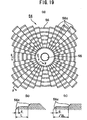
light nearly evenly. Namely, as shown in FIG.18 (a), a
circular reflection mirror 53 as the second reflection mirror
is divided into fan-shaped sections and a distance from LED
52 to reflection surface 53a is differentiated as shown in
FIG.18 (b), (c) and (d). Therefore, viewing from the top,
positions to reflect light are scattered in the circle and,
thereby, an effect that it appears glittering can be obtained.
Further, since LED 52 is provided with a small central radiation
surface 4a, its appearance becomes better. Namely, the
brightness of light to be externally radiated from the central
radiation surface 4a and the reflection surfaces 53a can be
equalized and luminescent spots can be arranged in good balance.
The brightness can be equalized by reducing the amount of light
to be externally radiated from the central radiation surface
4a to a small ratio such as less than 1/10 to that to be
externally radiated reflected by the circular reflection
mirror 53 after being radiated to the periphery of LED 52, i.e.,
by controlling most of light to be radiated to the periphery
of LED 52. Further, in detail, as the circular reflection
mirror 53 becomes bigger, the ratio of light to be externally
radiated from the central radiation surface 4a may be reduced.
Although the glittering effect can be obtained when the
reflection surface 53a is nearly planar or convex, the ratio
of light to be externally radiated from the central radiation
surface 4a may be reduced according as the curvature of convex
surface becomes larger. In modification 5, since light from
LED 52 is to be all reflected by the single-stage reflection
surface 53a at each fan-shaped section, it is desired that,
as shown in FIG. 18 (b), (c) and (d), the height of reflection
surface 53a is the same as the total height h of circular
stepwise reflection mirror 33 in the basic example as shown
in FIG.11 (b). Although the brightness is equalized in the
above example, the brightness may be accented such that it
becomes high toward the periphery or the other way around.
[Modification 6]
-
As shown in FIG.19, the sixth modification (54) of the
LED light 31 in embodiment 1B may be composed such that a
reflection mirror 56 as the second reflection mirror is divided
into fan-shaped sections with different lengths to allow the
shape of reflection mirror 56 to be close to a square as one
of polygons. Namely, as shown in FIG.19 (b) and (c), provided
that, in the shortest fan-shaped section, L is a length from
reflection surface 56a to the next reflection surface 56a, the
longest fan-shaped section separated 45 degrees from that
section is made to have a length of 2 L from reflection surface
56a to the next reflection surface 56a. Thereby, as shown in
FIG.13, when combining multiple square LED lights 41a, ..., it
is not necessary to cut a circular LED light into a square.
Therefore, reduction in external radiation efficiency can be
prevented and a combined light can be offered with higher
brightness. Further, when a nearly square LED is used as a
light source instead of a nearly cylindrical LED 55, there is
an advantage that a distance between the side of LED and
reflection mirror 56 becomes nearly equal over the
circumference.
[Embodiment 1C]
-
Embodiment 1C of the invention will be explained below
with reference to FIG.20.
-
As shown in FIG.20, LED 61 in embodiment 1C of the
invention is composed such that, of a pair of lead plates 63a,
63b, the lead plate 63a has a light emitting element 64 mounted
on its tip, and an upper electrode of light emitting element
64 is electrically connected through a wire 65 to the tip of
lead plate 63b. The tip portion of lead plates 63a, 63b, light
emitting element 64 and wire 65 as electric system are sealed
with transparent epoxy resin 66 as a light-transmitting
material. The transparent epoxy resin 66 is shaped such that
an upper portion of semisphere centered at the light emitting
element 64 is cut off like a circular cone. In this case,
although light radiated from the light emitting element 64 is
subjected to total reflection at upper surface 62 as the first
reflection mirror, its reflected light corresponds to
radiation light from a mirroring point of light emitting
element 64 to the upper surface and, therefore, it is not
converged and radiated from its side 67 while having a
divergence angle. Thus, it is needed that a circular stepwise
reflection mirror as the second reflection mirror for
reflecting light upward has a height in the Z-axis direction
greater than that for LED 32 in embodiment 1B.
-
In the case that a relatively wide light distribution
is allowed in LED light or a very low-profile shape is not
required in LED light, such the simple circular cone reflection
surface 62 can be used.
[Embodiment 1D]
-
Embodiment 1D of the invention will be explained below
with reference to FIG.21.
-
As shown in FIG.21, LED 70 in embodiment 1D of the
invention is composed such that, of a pair of lead plates 63a,
63b, the lead plate 63a has a light emitting element 64 mounted
on its tip, and an upper electrode of light emitting element
64 is electrically connected through a wire 65 to the tip of
lead plate 63b. The tip portion of lead plates 63a, 63b, light
emitting element 64 and wire 65 as electric system are sealed
with transparent epoxy resin 66. The transparent epoxy resin
66 is shaped like a regular cylinder and therefore the upper
surface of transparent epoxy resin 66 does not serve as the
first reflection mirror. Instead, an optical member 68 like
an umbrella molded with transparent acrylic resin is attached
through a light-transmitting material 67 onto the upper
surface of transparent epoxy resin 66. The optical member 68
has an upper surface 69 with a shape to be formed by rotating,
around the Z-axis, part of a parabola with a focal point at
the light emitting element 64 and with a symmetry axis on the
X-axis.
-
A lower surface 71 of the optical member 68 is formed
circular and stepwise with steps of about 45 degrees to replace
the circular stepwise reflection mirror in embodiment 2 (1B)
as the second reflection mirror. The lower surface 71 is
provided with aluminum evaporation 72 on which an overcoat (not
shown) is formed thereon to protect the aluminum evaporation
film. In the present embodiment 4 (1D), a degree of freedom
in overcoat after forming the evaporation mirror surface can
be increased. Namely, the overcoat may be colored and its
thickness is not limited.
-
The LED light 70 thus composed is operated such that a
predetermined voltage is applied to the pair of lead plates
63a, 63b, the light emitting element 64 emits light, light
heading upward directly goes straight because of not being
blocked, being externally radiated passing through a
transparent front plate (not shown). On the other hand, light
radiated between obliquely upward and sideward is entered into
the optical member 68 while passing through the
light-transmitting material 67. Light being irradiated to the
upper surface 69 as the first reflection mirror is subjected
to total reflection and is all reflected sideward nearly in
parallel with the X-Y plane since the upper surface 69 has a
shape to be formed by rotating, around the Z-axis, part of a
parabola with a focal point at the light emitting element 64.
Then, it is reflected upward nearly in parallel with the Z-axis
by the lower surface (circular stepwise reflection mirror) 71
as the second reflection mirror, being externally radiated
passing through the upper surface 69 and the front plate. In
like manner, light being directly irradiated to the lower
surface (circular stepwise reflection mirror) 71 is radiated
upward.
-
As described, the LED light in embodiment 1D can be
low-profile and can radiate light in a large area by using one
light emitting element while taking advantage, low-profile,
of LED, even when using a regular cylindrical LED and it can
offer high external radiation efficiency.
[Embodiment 1E]
-
Embodiment 1E of the invention will be explained below
with reference to FIG.22.
-
As shown in FIG. 22, an LED light 80 in embodiment 1E is
formed on an aluminum base 81 as a metal board. A circuit
pattern 83 is formed on the aluminum base 81 to sandwich an
insulation layer 82 and a light emitting element 84 is mounted
thereon while having electrical connection through a wire 85.
An optical member 87 like an umbrella concaved by a semisphere
91 molded with transparent acrylic resin is mounted on the
circuit pattern 83, light emitting element 84 and wire 85 as
electric system. In this case, transparent silicon resin as
light-transmitting material is filled in the semisphere 91 and
thereby the circuit pattern 83, light emitting element 84 and
wire 85 are sealed. In the state of being thus fixed, the
optical member 87 has an upper surface 88 with a shape to be
formed by rotating, around the Z-axis, part of a parabola with
a focal point at the light emitting element 84.
-
A lower surface 89 of the optical member 88 is formed
circular and stepwise with steps of about 45 degrees to serve
as the second reflection mirror. The lower surface 89 is
provided with aluminum evaporation 90 on which an overcoat (not
shown) is formed thereon to protect the aluminum evaporation
film. Also in the present embodiment 1E, a degree of freedom
in overcoat after forming the evaporation mirror surface can
be increased. Namely, the overcoat may be colored and its
thickness is not limited.
-
The LED light 80 thus composed is operated such that the
light emitting element 84 emits light, light heading upward
directly goes straight because of not being blocked, being
externally radiated passing through a transparent front plate
(not shown). On the other hand, light radiated between
obliquely upward and sideward is entered into the optical
member 87 while passing through the light-transmitting
material 86. Light being irradiated to the upper surface 88
as the first reflection mirror is subjected to total reflection
and is all reflected sideward nearly in parallel with the X-Y
plane since the upper surface 88 has a shape to be formed by
rotating, around the Z-axis, part of a parabola with a focal
point at the light emitting element 84. Then, it is reflected
upward nearly in parallel with the Z-axis by the circular
stepwise reflection mirror 89 as the second reflection mirror,
being externally radiated passing through the upper surface
88 and the front plate. In like manner, light being directly
irradiated to the circular stepwise reflection mirror 89 is
radiated upward.
-
The LED light 80 in the present embodiment 1E is mounted
on the aluminum base 81 with a good thermal conductivity and
thereby the heat radiation property can be significantly
enhanced. Thus, even when large current is flown through the
light emitting element 84, heat saturation does not occur.
Therefore, a large optical output can be obtained.
-
As described, the LED light in embodiment 1E can be
low-profile, with high brightness and can radiate light in a
large area as well as having an enhanced heat radiation property
and offering a large optical output without being affected by
heat saturation.
[Embodiment 1F]
-
Embodiment 1F of the invention will be explained below
with reference to FIG.23.
-
As shown in FIG.23, an LED light 100 in embodiment 1F
is also formed on an aluminum base 95 as a metal board. A
circuit pattern 97 is formed on the aluminum base 95 to sandwich
an insulation layer 96 and a light emitting element 98 is
mounted thereon while having electrical connection through a
wire 99. The circuit pattern 97, light emitting element 98
and wire 99 as electric system are sealed with transparent epoxy
resin 102 as a light-transmitting material. An optical member
101 molded with circular transparent acrylic resin is mounted
thereon. In the state of being thus fixed, the optical member
101 has an upper surface 103 with a shape to be formed by
rotating, around the Z-axis, part of a parabola with a focal
point at the light emitting element 98, and it serves as the
first reflection mirror.
-
A lower surface 104 of the optical member 101 is formed
circular and stepwise with steps of about 45 degrees to serve
as the second reflection mirror. In the LED light 100 of the
present embodiment 1F, the lower surface 104 is not provided
with metal evaporation. Namely, light from the light emitting
element 98 to be reflected sideward by the upper surface 103
of optical member 101 as the first reflection mirror is
reflected upward due to total reflection at the lower surface
104 of optical member 101 as the second reflection mirror.
Thus, even without metal evaporation formed on the lower
surface 104 of optical member 101, most of light can be
reflected upward only by the total reflection at the lower
surface 104. In order to reflect light that passes through
the lower surface 104 without being subjected to the total
reflection, a supplemental reflection member 105 is mounted
on the circuit board 97 while providing an air layer under the
lower surface of optical member 101. The supplemental
reflection member 105 has an upper surface with a reflection
surface formed thereon by plating and serves to upwardly
reflect light passing through the lower surface 104.
-
In the LED light 100 of the present embodiment 1F, it
is not necessary to provide the metal evaporation with the lower
surface 104 of optical member 104 that serves both as the first
reflection mirror and as the second reflection mirror, and the
supplemental reflection member 105 with coating formed by
simple plating only has to be provided to allow almost all of
light emitted from the light emitting element 98 to be upwardly
radiated. Thus, the high external radiation efficiency can
be obtained.
-
The LED light 100 in the present embodiment 1F is also
mounted on the aluminum base 95 with a good thermal conductivity
and thereby the heat radiation property can be significantly
enhanced. Thus, even when large current is flown through the
light emitting element 98, heat saturation does not occur.
Therefore, a large optical output can be obtained.
-
As described, the LED light in embodiment 1F be
low-profile, with high brightness and can have the high
external radiation efficiency by using the simple process as
well as having an enhanced heat radiation property and offering
a large optical output without being affected by heat
saturation.
[Embodiment 1G]
-
Embodiment 1G of the invention will be explained below
with reference to FIG.24.
-
As shown in FIG.24, an LED light 110 in embodiment 1G
is composed of: an optical member 111 that is molded with
transparent acrylic resin and has a lower surface 113 which
is a stepwise reflection surface to serve as the second
reflection mirror and a cylindrical space 114 formed at the
center; and LED 32, like the LED light 31 in embodiment 1B,
that is fixed in the space 114 at the center. Namely, the LED
32 is composed such that a light emitting element 115 etc. are
sealed with transparent epoxy resin and has a paraboloid 116
at the upper surface as the first reflection mirror. Light
to be radiated from the light emitting element 115 and sideward
reflected by the upper surface 116 is upwardly reflected by
the lower surface 113 of optical member 111 and then externally
radiated passing through a front plate (not shown).
-
In the LED light 31 of embodiment 2 (1B), light to be
directly (without being reflected by the upper surface 116)
radiated from upper portion of the side surface 117 of LED 32
is not utilized without being upwardly reflected while
proceeding along a path indicated by a two-dotted line.
However, in the LED light 110 of the present embodiment 1G,
it can be utilized such that it is, as indicated by a dotted
line, reflected by the horizontal upper surface 112 of optical
member 111 and then reflected upwardly by the lower surface
113. Thus, the LED light can be low-profile and with further
enhanced external radiation efficiency. Further, light to be
entered into the space 114 is refracted in a direction to give
a large angle to the Z-axis and thereby the brightness at the
periphery in viewing from the top in FIG. 24 (a) can be enhanced.
-
In the above embodiments, transparent acrylic resin is
used for the optical member that serves as the second reflection
mirror or both as the first reflection mirror and as the second
reflection mirror. However, the other material such as
another transparent synthetic resin may be used for that.
-
Although the above embodiments explain that the central
radiation surface is provided to take out light radiated from
the center of LED, light radiated from the center of LED may
be taken out without the central radiation surface by using
a large size light emitting element or placing the upper surface
optical system just nearby to make an incident angle from the
light emitting element to the upper surface optical system to
be within a critical angle.
-
Alternatively, when using a light emitting element with
a narrow light distribution, a sufficient lateral radiation
can be obtained without always placing the upper surface
optical system nearby.
-
The composition, shape, number, material, dimensions,
connection form etc. of the other part in the LED light are
not limited to those described in the above embodiments.
[Embodiment 2A]
-
FIG.25 (a) is a plain view showing an LED light 201 in
embodiment 2A of the invention, (b) is a cross sectional view
cut along the line A-A in (a), and (c) is an enlarged cross
sectional view showing part P of (b). The LED light 201 is
composed of: an LED 202 that has a light emitting element 206
with a predetermined light distribution characteristic at the
center of a disk-shaped body; and a reflection mirror 203 that
has a concentric and stepwise reflection surface 203a around
the LED 202.
-
The reflection mirror 203 is molded of transparent
acrylic resin and, after molding, the reflection surface 203a
is formed by providing aluminum evaporation thereon to
mirror-finish it. The reflection surface 203a is, as shown
in FIG. 25 (a) , inclined about 45 degrees to the X-Y plane such
that light to be entered from the X(Y) direction is reflected
to the Z-axis direction.
-
FIG.26 (a) is a cross sectional view showing the LED 202,
(b) is a plain view thereof, and (c) is a side view thereof.
The LED 202 is composed of: lead frames 205a, 205b; a light
emitting element 206; a bonding wire 207 to provide electrical
connection between the lead frame 205b and light emitting
element 206; transparent epoxy resin 208 that is with an optical
surface while integrally sealing the lead frames 205a, 205b
and light emitting element 206; a reflection mirror 209 that
has a central radiation surface 209a and a reflection surface
209b; and a radiation surface 210 that composes part of a sphere
centered at the light emitting element 206 to radiate light
in the X-Y direction.
-
The lead frames 205a, 205b are of copper alloy and
disposed having a gap for insulation on the X-Y plane, and the
lead frame 205a with a large area has the light emitting element
206 mounted on an origin position thereof.
-
The light emitting element 206 is formed cubic, face-up
bonded to the lead frame 205a and provided with an emission
surface on its top. It is of large current type (high output
type) in order to keep the emission intensity of LED 202 at
a predetermined value while reducing the number of elements
used as much as possible. The light emitting element 206 may
be flip-chip mounted on the lead frame 205a.
-
The transparent epoxy resin 208 is of epoxy resin with
a refractive index of 1.55 and has the central radiation surface
209a at the center (directly over the light emitting element
206) of upper surface thereof. The reflection mirror 209 is
constructed such that the reflection surface 209b is formed
continuously with the central radiation surface 209a. A
proximity optical system is formed by disposing the light
emitting element 206 close to the reflection mirror 209 and
then integrally molding with resin.
-
The reflection mirror 209 is composed of the central
radiation surface 209a to radiate directly upwardly light
radiated from the light emitting element 206, and the
reflection surface 209 b that has a circular reflection shape
to be formed by rotating, around the center axis Z, part of
a parabola with a focal point at the center of emission surface
of light emitting element 206 as the coordinate origin in FIG. 26
and with a symmetry axis on the X-axis. Alternatively,
according to use, the reflection mirror 209 may be not provided
with the central radiation surface 209a.
-
The reflection mirror 209 is the first reflection mirror
to reflect light radiated from the light emitting element 206.
As shown in FIG. 26 (c) , the radius R of reflection surface 209b
is given such that almost all of light being radiated with a
large sold angle to the light emitting element 206 can be
effectively radiated sideward. In this example, where a
height from the emission surface of light emitting element 206
to the edge of reflection mirror 209 in the Z-axis direction,
H=2.0 mm and R=3.5 mm are given, the relationship between the
edge height H of reflection mirror 209 and radius R is H<R.
Further, in order to form a proximity optical system to provide
a relatively large solid angle, the distance (thickness of
transparent epoxy resin 208) h between the light emitting
element 206 and the central radiation surface 209a is set to
be 0.5 mm.
-
FIG.27 shows the composition of light emitting element
206. In the order of the bottom layer to the top layer, n-GaAs
substrate 221, n-AlInGaP cladding layer 222, a layer 223
including a light emitting layer, p-AlInGaP cladding layer 224
and p-GaP window layer 225 are formed. On the p-GaP window
layer 225, Al bonding pad (positive electrode) 227 is formed
through AuZn contact layer 226 for the ohmic contact with the
window layer 225. Further, under the n-GaAs substrate 221,
Au alloy electrodes (negative electrodes) 228 are formed. The
n-GaAs 221 substrate is not transparent to a wavelength of light
emitted from the light emitting layer. The n-AlInGaP cladding
layer 222 and p-AlInGaP cladding layer 224 are transparent
thereto.
-
FIG.28 is an illustration showing a light distribution
characteristic of the light emitting element 206. A radiation
intensity to be radiated from the top surface 206a and side
surfaces 206b (four side surfaces) of light emitting element
206 is the sum of radiation intensity to be radiated from the
top surface 206a and radiation intensity to be radiated from
the four side surfaces 206b. The light distribution
characteristic I () is represented by the next formula (1) :
I()=k · cos + (1-k) · sin
where k·cos indicates radiation intensity to be radiated from
the top surface 206a and (1-k) · sin indicates radiation
intensity to be radiated from the side surface 206b. is an
angle to the Z-axis in light emitting element 206. As k is
changed, the distribution of light to be radiated from the top
surface 206a and light to be radiated from the side surface
206b is changed.
-
FIG.29 shows a change in radiation intensity (in the
Z-axis direction) when is changed in light emitting element
206 with different light distribution characteristics based
on the above formula (1). FIG.29 (a) shows a definition of
angle to the light emitting element 206. FIG.29 (b) shows the
state (top 100%) of light of 100% being radiated from the top
surface 206a at k=1. FIG.29 (c) shows the state (top 80%) of
light of 80% being radiated from the top surface 206a at k=0.8
and light of 20% being radiated from the side surface 206b.
FIG.29 (d) shows the state (top 60%) of light of 60% being
radiated from the top surface 206a at k=0.6 and light of 40%
being radiated from the side surface 206b.
-
The light emitting element 206 has a characteristic at
about k=0.8 that the ratio of light radiated from the top
surface to light emitted from the layer 223 including light
emitting layer becomes big since n-GaAs substrate 221 is a black
absorbing material to emission color. Namely, light of 80%
is radiated from the top surface 206a and light of 5% is radiated
from each side surface 206b. In order to have a desired light
distribution characteristic, the thickness of epitaxial layer
or the shape of light emitting element 206 is controlled.
-
The light emitting element 206 with a light distribution
characteristic as shown in FIG.29 (b) is characterized such
that light is radiated from the top surface 206a, the radiation
intensity lowers as increases and it becomes nearly zero
at =90 degrees. The light emitting element 206 with a light
distribution characteristic as shown in FIG.29 (c) is
characterized such that light is also radiated from the side
surface 206b, radiation intensity at =0 is smaller than that
of the light emitting element in FIG.29 (b) and it however does
not become zero even at 90 degrees and therefore light is
radiated in the X-Y direction. The light emitting element 206
with a light distribution characteristic as shown in FIG.29
(d) is characterized such that the amount of light radiated
from the side surface 206b is greater than that in FIG.29 (c)
and, therefore, radiation intensity at =0 is smaller and,
however, a reduction in radiation intensity along with a change
of is smaller than that in FIG.29 (b) and (c), and it does
not become zero even at 90 degrees and therefore light is
radiated in the X-Y direction.
-
The light distribution characteristic of LED 202 depends
on the light distribution characteristic of light emitting
element 206, a position precision of optical surface in the
light emitting element 206, central radiation surface 209a,
reflection surface 209b and radiation surface 210, a mounting
position precision of the light emitting element 206 to the
lead frame 205a, and a setting position precision of the lead
frame 205a and above optical surface to a die in molding
integrally with resin. In order not to cause an unevenness
in light distribution in direction as shown in FIG.26 (b),
evenness in light to be radiated in the circumference direction
(360 degrees) of radiation surface 210 centered at the Z-axis
is required. If a displacement exists between the light
emitting element 206 and optical surface, unevenness In Light
Distribution in direction is generated according to the
amount of displacement. Especially, the proximity optical
system of LED 202 in the invention has such a compositional
characteristic that it is likely to generate unevenness in
light distribution due to a slight displacement.
-
FIG.30 shows a change in light amount of light radiated
directly upward from the LED 202 and light irradiated to the
reflection surface 203a, caused by a change in light
distribution characteristic generated when, in the LED 202,
the center axis of light emitting element 206 is displaced in
the X-axis direction to the optical surface. In the case of
light emitting element 206 with GaAs substrate, the effective
radiation efficiency ratio lowers when a displacement is
generated in the X-axis direction in manufacture. In FIG. 30,
it significantly lowers, particularly, more than 0.3 mm.
-
FIG.31 (a) and (b) show observation conditions of light
amount radiated from LED 202, where the entire circumference
of LED 202 is divided into ij to represent 32 regions. As
shown in FIG.31 (a) , its circumference of 360 degrees centered
at the Z-axis is divided into eight sections (j=1 to 8). FIG.31
(b) shows an angle range of 0 to 20 degrees (i=1) to the Z-axis,
an angle range of 20 to 60 degrees (i=2), an angle range of
60 to 100 degrees (i=3) , and an angle range of 100 to 180 degrees
(i=4). The amount of light radiated from LED 202 to theses
regions will be explained below. Herein, it is assumed that
a region in angle range of 0 to 20 degrees to the Z-axis
corresponds to light to be directly externally radiated near
the Z-axis from LED 202 and a region in angle range of 60 to
100 degrees to the Z-axis corresponds to light to be radiated
from LED 202 to the reflection mirror 203 then reflected in
a direction near the Z-axis by the reflection mirror 203 to
be radiated externally.
-
FIG.32 shows a deviation in total light amount of LED
202 in using the light emitting element 206 with a top light
distribution characteristic of 100% under the observation
conditions as shown in FIG.31. The deviation of total light
amount is calculated under conditions that six displacements
of 0.0 to 0.5 mm in the X-axis direction are generated, and
the deviation of total light amount in each direction is shown
connected with lines. As the amount of displacement increases,
the deviation of total light amount increases. FIG.32 (b)
shows a deviation in total light amount of LED 202 in using
the light emitting element 206 with a top light distribution
characteristic of 80%. Since the light emitting element 206
has a structure to radiate light from the side surface 206b,
the deviation of total light amount is improved.
-
As described above, as the amount of light radiated
laterally from the light emitting element 206 increases, the
deviation of total light amount in effective radiation range
due to a displacement between the light emitting element 206
and optical surface is reduced. Therefore, when using a light
emitting element 206 with a light distribution characteristic
of less than k=0.8, the deviation of total light amount in
effective radiation range is almost removed and no visual
influence is generated. This is because, even when the
position of a light emitting element 206 mounted on the lead
frame 205a is deviated within 0.1 mm in the X-axis (Y-axis)
direction from the Z-axis, its influence can be compensated
by the light distribution characteristic of light emitting
element 206.
-
The LED 202 may be fabricated by, e.g. , transfer molding
as explained referring to FIG.9.
-
The operation of LED light 201 will be explained below.
-
When an operator turns on a power switch (not shown) of
LED light 201, power source section (not shown) applies a
voltage to the lead frames 205a, 205b. The light emitting
element 206 emits light based on the applying of voltage.
Light emitted directly upward along the Z-axis from the light
emitting element 206 is externally radiated out of the
transparent epoxy resin 208 from the central radiation surface
209a. 50 to 60% of light to be emitted from the light emitting
element 206 is irradiated to the reflection surface 209b with
a solid angle of about 2.7 strad to the light emitting element
206. Light to be emitted in a direction nearly horizontal from
the light emitting element 206 is directly irradiated to the
radiation surface 210, directly radiated externally in a
direction nearly parallel to the X-Y plane from the radiation
surface 210.
-
Light to be radiated nearly parallel to the X-Y plane
from the LED 202 is reflected nearly in the Z-axis direction
by the reflection surface 203a of reflection mirror 203, then
radiated externally.
-
As described above, the LED light 201 in embodiment 2A
described above is composed such that the light emitting
element 206 of LED 202 composing a proximity optical system
has a light distribution characteristic of less than k=0.8 in
I() = k · cos + (1-k) · sin and the light emitting element 206
and optical surface are integrally formed by transfer molding.
Light in the X-axis direction to be radiated from the LED 202
and irradiated to the reflection mirror 203 has little
deviation of total light amount in effective radiation range
and can be radiated almost evenly in the Z-axis direction by
the reflection mirror 203. Thereby, a low-profile lamp with
a good appearance can be offered while having a large area of
reflection mirror and no difference in surface brightness.
When it is applied to a tail lamp or a brake lamp of automobile,
visibility of light can be enhanced not only in the back
direction of automobile but also in the lateral direction
thereof.
-
Although the above LED light 201 is exemplified such that
the LED 202 uses the light emitting element 206 with a light
distribution characteristic of k=0.8, if it uses a light
emitting element 206 with a light distribution characteristic
of less than k=0.8, then the deviation of total light amount
in effective radiation range due to a displacement between the
light emitting element 206 and optical surface can be reduced
to a level causing no problem practically.
-
In the manufacture by transfer molding, transparent
epoxy resin 208 is injected into a die while sandwiching the
lead frames 205a, 205b by the die. Therefore, the positioning
between the light emitting element 206 and optical surface can
be performed at a high precision of ±0.1 mm. Thereby, even
when using the proximity optical system composed of a light
emitting element 206 with k=0.8, the LED light 201 with a
stabilized quality can be offered while preventing a
dispersion in light distribution characteristic due to an
individual difference of the LED 202.
-
Although in the above explanation transparent epoxy
resin 208 is used as the transparent material to seal the light
emitting element 206, another transparent material having
about the same transparency and the other optical
characteristics may be used. Further, although transparent
acrylic resin is used for the reflection mirror 203, the other
material such as another transparent synthetic resin may be
used for that.
-
The composition, shape, number, material, dimensions,
connection form etc. of the other part in the LED light are
not limited to those described in the above embodiments.
-
Although the reflection surface 209b is provided to offer
the total reflection of resin without being mirror fished, it
may be alternatively mirror finished by metal evaporation etc.
[Embodiment 2B]
-
FIG.33 (a) is a plain view showing an LED 202a in
embodiment 2B of the invention in viewing from the Z-axis
direction, and (b) is a cross sectional view showing the
vicinity of a light emitting element 206 in (a). The LED 202a
is composed of: the light emitting element 206 that is of GaP
substrate AlInGaP using a n-GaP substrate with a transparency
and has a light distribution characteristic of top 60% (k=0.6);
and lead frames 205b, 205c that are of copper alloy and folded
at its resin-sealed region. The light emitting element 206
is mounted on the tip of lead frame 205c. Like parts are
indicated by the same numerals used in embodiment 2A and the
explanations thereof are omitted here.
-
FIG.34 shows a deviation in total light amount of LED
202a using a light emitting element 206 with a light
distribution characteristic of k=0.6. As shown, even when
X=0.4, the deviation in light distribution characteristic is
kept within ±20% since the amount of light to be radiated from
the side surface 206b of light emitting element 206 is increased,
as compared to the light emitting element 206 with a light
distribution characteristic of k=0.8. Thus, the deviation in
total light amount is improved. The light emitting element
206 with k=0.6 may be formed using a substrate material that
offers a light transparency to emission color of GaP etc. in
order to increase the radiation amount from the side surface
206b based on a reflection in of the light emitting element
206.
-
LED 202a may be fabricated by, e.g., casting mold as
explained referring to FIG.10.
-
Since the LED 202a in embodiment 2B has the light emitting
element 206 using the n-GaP substrate with a transparency and
it has a light distribution characteristic of k=0.6, it can
have a wider light distribution characteristic than LED 202
with the light emitting element 206 using the n-GaAs substrate.
Thereby, even if a small displacement is generated between the
light emitting element 206 and optical surface, the deviation
of total light amount in effective radiation range can be
reduced to a level causing no problem practically.
-
In the casting mold, since the tip (free and) of lead
frames 205b, 205c is not restrained by the casting, precision
in positioning between the light emitting element 206 and
optical surface lowers to ± 0.2 mm as compared to that in the
transfer molding. Especially, when the light emitting element
206 is mounted on the tip thick portion of planar lead frame,
it is difficult to obtain a high precision in positioning.
However, since the tolerance of precision in positioning is
increased, the productivity can be enhanced and therefore it
has an excellent mass production property. By curing the
transparent epoxy resin 208 for long hours, unevenness in
thermal stress is reduced and the lead frames 205b, 205c are
not likely to be released from the transparent epoxy resin 208.
Meanwhile, by choosing the fabrication process management and
the light distribution characteristic of light emitting
element 206, the light distribution characteristic can be
stabilized.
[Embodiment 2C]
-
FIG.35 (a) is a plain view showing an LED 202b in
embodiment 2C of the invention in viewing from the Z-axis
direction, and (b) is a cross sectional view showing the
vicinity of a light emitting element 206 in (a). The LED 202b
is composed of: the light emitting element 206 that is of GaP
substrate AlInGaP using a n-GaP substrate with a transparency
and has a light distribution characteristic of top 40% (k=0.4) ;
and lead frames 205b, 205d that are of copper alloy. Like parts
are indicated by the same numerals used in embodiments 2A, 2B
and the explanations thereof are omitted here.
-
The light emitting element 206 with k=0.4 has dimensions
(e.g., 0.3 mm square) smaller than the light emitting element
206 with k=0.6, and thereby the radiation amount from the side
surface 206b is further increased since the absorption loss
in light emitting element is reduced.
-
The light emitting element 206 is mounted on the tip of
lead frame 205c punched out by pressing.
-
Since the LED 202b in embodiment 2C has the light emitting
element 206 mounted on the tip of lead frame 205c, it can have
a reduced contact area between the lead frames 205b, 205d and
transparent epoxy resin 208, thereby preventing the releasing,
as well as having an excellent mass production property while
reducing the deviation in total light amount in effective
radiation range. Further, the process of folding the lead
frames 205b, 205d is not needed and therefore the productivity
can be enhanced.
-
Further, since the LED 202b in embodiment 2C has the light
emitting element 206 using the n-GaP substrate with a
transparency, it can have a wider light distribution
characteristic than LED 202 with the light emitting element
206 using the n-GaAs substrate, like embodiment 2B. Thereby,
even if a small displacement is generated between the light
emitting element 206 and optical surface, the deviation of
total light amount in effective radiation range can be reduced
to a level causing no problem practically.
[Embodiment 2D]
-
FIG.36 shows an LED 202c in embodiment 2D of the invention.
The LED 202C is composed of: a light emitting element 206 of
Al2O3 substrate GaN; lead frames 205b, 205d that are of copper
alloy and folded at its resin-sealed region; and transparent
epoxy resin 208 with an optical surface. The light emitting
element 206 is mounted on the tip of lead frame 205d. The light
emitting element 206 is sealed with sealing resin 208s
including phosphor. In FIG.36, the transparent epoxy resin
208 is shown as transparent member. Like parts are indicated
by the same numerals used in embodiment 2A, 2B, 2C and the
explanations thereof are omitted here.
-
Since the LED 202c in embodiment 2D has the light emitting
element 206 that is mounted on the tip of lead frame 205d and
sealed with sealing resin 208s in the shape of a semisphere,
even when the light emitting element 206 does not have a wide
light distribution characteristic, excitation light to be
radiated from phosphor can be diffused. Thereby, its light
distribution characteristic can be made to be suitable for the
proximity optical system of the invention.
-
The phosphor available is Ce:YAG (yttrium aluminum
garnet) etc. In order to enhance the light distribution
characteristic, a light diffusion material for diffusing light
may be mixed into the sealing resin 208s instead of the phosphor.
Thereby, the same effect can be obtained. The light diffusion
material may be, e.g., titanium oxide, alumina, SiO2.
-
Although in the above embodiments 2A to 2D the light
emitting element 206 uses a GaAs system substrate, it may use
a GaP substrate AlInGaP system or GaN system according to the
light distribution characteristic. Further, it may
selectively use a substrate with a transparency or
non-transparency to emission wavelength. If applicable to the
LED light 201, the light emitting element 206 is not limited
to specific composition.
-
Although the light emitting diode is formed by molding
the reflection surface and side reflection surface while
sealing the light emitting element, it may be formed by sealing
the light emitting element with a light-transmitting material
while mounting a mold with reflection surface and side
reflection surface being separately formed using transparent
resin thereon. Thus, a proximity optical system to the light
emitting element can be formed.
-
In the above embodiments 2A to 2D, the reflection mirror
209 has a circular reflection shape to be formed by rotating,
around the Z-axis, part of a parabola with a focal point at
the origin of light emitting element 206 and with a symmetry
axis on the X-axis, and the radiation surface 210 has a shape
to compose part of a spherical surface centered at the light
emitting element 206. However, they are not specifically
limited thereto if they are formed to radiate light being
emitted from the light emitting element 206 in the side surface
direction. Especially, in the shape of transparent epoxy
resin 208 in the above embodiments or when the relationship
of H<R is established, the reflection mirror 209 is placed close
to the light emitting element 206 and thereby the same effect
can be obtained in aspect of stabilization of light
distribution characteristic in LED based on the positional
precision of optical system. Even when the relationship of
H<R is not satisfied, if h<1 mm, the same effect can be obtained.
[Embodiment 3A]
-
FIG.37 shows an LED in embodiment 3A of the invention,
wherein (a) is a cross sectional view thereof, and (b) is a
plain view thereof.
-
As shown in FIG.37, the LED 302 in embodiment 3A has an
integrated structure that a light emitting element 306 as a
light source is sealed with transparent epoxy resin 308 while
forming optical surface. In the explanation below, the center
axis of light emitting element 306 is a Z-axis, a point on the
top surface of light emitting element and on the Z-axis is an
origin, and a coordinate system with an X-axis and a Y-axis
orthogonal to the Z-axis at the origin is defined. Meanwhile,
the Z-axis is also called center axis Z.
-
The LED 302 is composed such that the light emitting
element 306 is, at the origin, mounted through Ag paste on a
lead frame 305a of a pair of lead frames 305a, 305b that are
of copper alloy and disposed through a gap for insulation on
the X-Y plane, the upper surface electrode of light emitting
element 306 is bonded through a gold wire 307 to the tip of
lead frame 305b, and part of lead frames 305a, 305b, light
emitting element 306 and wire 307 are sealed with transparent
epoxy resin 308 (refractive index 1.55) while molding the
optical surface.
-
The main feature of LED 302 is the shape of transparent
epoxy resin 308. Namely, the transparent epoxy resin 308 has
a central radiation surface 309a at the center of its upper
surface (directly over the light emitting element 306) and a
reflection surface 309b formed subsequently to the central
radiation surface 309a to compose a reflection mirror 309.
-
The reflection surface 309b has a circular reflection
shape to be formed by rotating, around the Z-axis, part of a
parabola with a focal point at the origin and with a symmetry
axis on the X-axis. The central radiation surface 309a is an
optical surface to radiate light to be emitted from the light
emitting element 306 in the Z-axis direction and may be formed
concave or convex. According to use, the central radiation
surface 309a may be not formed.
-
The reflection surface 309b has a solid angle of 2π
{1-cosc} or greater, where c is a critical angle of the
abovementioned transparent material. Alternatively, an
angle 1 of an oblique line L1 to connect between the focal
point of light emitting element 306 and the edge of reflection
surface 309b to the Z-axis is set to be greater than (90 degrees
-c).
-
A diameter W of the reflection surface 309b is preferably
less than 10 mm. This is because, when the transparent epoxy
resin 308 has a large size, though it is advantageous in optical
design, a crack may be generated due to a thermal shock by
remaining stress in resin curing and therefore the transparent
epoxy resin 308 preferably has a small size.
-
The transparent epoxy resin 308 has a side radiation
surface 310 to compose part of a spherical surface centered
at the origin. A height H to vertically connect between the
edge of reflection surface 309b at the reflection surface 310
and the X-axis to be horizontally extended from the focal point
of light emitting element 306 is set such that an angle 2
to the X-axis of the oblique line L1 connecting between the
focal point of light emitting element 306 and the edge of
reflection surface 309b is less than the critical angle
c. The angle 2 is preferably less than (c -5 degrees).
This is because, even when an incident angle does not reach
c, the interface reflection is likely to occur near c as
shown in FIG.38.
-
Although the abovementioned (90 degrees - c) or 2π
{1-cos c} means having a large solid angle to the light
emitting element 306, it also means a range that the interface
reflection of light being directly irradiated from the light
emitting element 306 to the side radiation surface 310 can be
prevented in order not to be stray light. Even if the side
radiation surface 310 is a vertical surface with no taper, when
1 is greater than (90 degrees -c), 1 becomes less than
c and thereby no stray light due to total reflection is
generated.
-
The LED 302 has such dimensions that the diameter is 10
mm, the diameter W of reflection surface 309b is 9 mm, the height
H of outer edge in the Z-axis direction, and the angle 1
to the Z-axis of the line from the top surface of light emitting
element 306 to the edge of reflection surface 309b is 70
degrees.
-
The lead frame 305a with the light emitting element 306
mounted thereon is composed such that part of the lead frame
305a embedded in transparent epoxy resin 308 is reduced as much
as possible to the extent that the wire 307 is not exposed,
by drawing it out of transparent epoxy resin 308 under the mount
surface from the vicinity of the mount position of light
emitting element 306. The lead frame 305b is also in the shape
of a strip-like plate and is disposed parallel to part of the
lead frame 305a being drawn out of the resin.
-
Since the LED 302 of a type to radiate light in a direction
perpendicular to the Z-axis, called side radiation type,
requires a wide radiation range and sufficient radiation
intensity, the light emitting element 306 used is of large
current type (high-output type).
-
For example, as shown in FIG.39, it is composed of
n-AlInGaP cladding layer 312, layer 313 including a light
emitting layer, AlInGaP cladding layer 314 and p-GaP window
layer 315 that are sequentially formed on n-GaP substrate 311.
Further, an Al bonding pad (positive electrode) 317 is formed
through AuZn contact 316 for the ohmic contact with the window
layer 315 on the p-GaP window layer 315. Further, Au alloy
electrodes (negative electrodes) 228 are formed under the
n-GaP substrate 311.
-
The light emitting element 306 with the negative
electrodes 318 is mounted on the lead frame 305a, and the
positive electrode 317 thereof is bonded through the wire 307
to the tip of lead frame 305b. By applying a predetermined
voltage between the electrodes 317 and 318, the light emitting
element 306 emits light. The emission of light is generated
such that carriers (electron and hole) are confined in the layer
313 including the light emitting layer by the cladding layers
312, 314 and the carriers are recombined in the layer 313
including the light emitting layer.
-
The light emitting element 306 has a large heat release
value since it is of large current type. In embodiment 3A,
the lead frames 305a, 305b where to mount the light emitting
element 306 are of a copper alloy material with a high thermal
conductivity (300 W/m · k or higher) and the heat radiation
property is enhanced by reducing the embedded portion as much
as possible as shown in FIG.37. Thus, by reducing heat to be
accumulated in the light emitting element 306 and lead frame
305a as much as possible, the temperature rise of light emitting
element 306 can be suppressed and the reduction of light output
in LED 302, which has a negative light output dependency to
temperature, can be prevented. Therefore, the LED 302 can
offer a high light output by setting a large supply current.
For example, a large amount of light can be obtained by
supplying a large current of more than 100 mA.
-
The emission operation of LED 302 thus composed will be
explained below.
-
When a voltage is applied to the lead frames 305a, 305b
of LED 302, the light emitting element 306 emits light. Of
light to be emitted from the light emitting element 306, light
emitted directly upward along the Z-axis from the light
emitting element 306 is externally radiated from the central
radiation surface 309a while being directly transmitted
through the transparent epoxy resin 308. Further, of light
to be emitted from the light emitting element 306, light to
reach the reflection surface 309b is all subjected to total
reflection due to its large incident angle to the reflection
surface 309b, then heading to the side radiation surface 310.
Since the reflection surface 309b has the reflection shape
described earlier, light being reflected by the reflection
surface 309b is all radiated nearly in parallel with the X-Y
plane. Since the side radiation surface 310 composes part of
spherical surface centered at the light emitting element 306,
the light being radiated nearly in parallel is radiated forming
nearly a plane in directions of 360 degrees around the Z-axis
though it is slightly refracted by the side radiation surface
310.
-
FIG.40 (a), (b) and (c) are characteristic diagrams
showing a light intensity distribution, a light flux
distribution, and a light flux integration in a standard light
emitting element. The lateral axis indicates an angle to the
center axis, and the vertical axes indicate light intensity
ratio, light flux ratio and light flux ratio, respectively.
Since 1 of the outer edge to the Z-axis is 70 degrees, about
80% of light to be emitted from the light emitting element is
reflected reaching the reflection surface 309b, then radiated
forming nearly a plane from the side radiation surface 310.
The remaining part of about 20% is radiated in a direction of
70 degrees to the Z-axis without being refracted by the side
radiation surface 310.
-
As described above, in the LED 302 of embodiment 3A, light
to be emitted from the light emitting element 306 can be
laterally radiated at an ideal efficiency because: the light
emitting element as a light source is sealed with transparent
epoxy resin 308; the central radiation surface 309a,
reflection surface 309b and side radiation surface 310 as
optical surfaces are molded; and the reflection surface 309b
has a shape to be formed by rotating, around the center axis
Z, part of a parabola with a focal point at the origin of light
emitting element 306 and with a symmetry axis on the x-axis.
-
Further, since the side radiation surface 310 of
transparent epoxy resin is formed composing part of spherical
surface centered at the light emitting element 306, light being
reflected by the reflection surface 309b and radiated nearly
in parallel proceeds directly through the side radiation
surface 310 and then externally radiated forming nearly a plane
in directions of 360 degrees around the Z-axis, and light
directly heading to the side radiation surface 310 from the
light emitting element 306 is externally radiated directly
without being refracted by the side radiation surface 310.
Thus, since no light to be radiated in the range of a small
angle to the Z-axis exists, the radiation efficiency of light
to be externally radiated in the lateral direction while being
controlled as primary light from the side radiation surface
310 can be significantly enhanced.
-
Further, since the side radiation surface 310 of
transparent epoxy resin 308 composes part of spherical surface
centered at the light emitting element 306, the side radiation
surface 310 is in the shape of a taper. Therefore, the release
from a die in potting mold or casting mold can be facilitated
without breaking the transparent epoxy resin 308. In the case
of an inverted taper or vertical wall, the release from a die
cannot be facilitated and the transparent epoxy resin 308 may
be broken. Thus, it can be made by using a manufacturing method
and resin material generally available, and thereby its mass
production property and stability in characteristic can be
enhanced.
-
The side radiation surface 310 may be formed by using
part of circular cone surface that is slightly inclined (e.g.,
a slope of about 4 degrees) to the center of a cylinder, other
than the spherical surface. Also in this shape, the release
from a die can be facilitated without breaking the transparent
epoxy resin 308. Another shape to facilitate the release from
a die may be also used.
-
The LED 302 can be formed further low-profile by
providing the central radiation surface 309a at the center of
reflection surface 309b, i.e., directly over the light
emitting element 306 and by curving the reflection surface 309b
from the circumference edge of central radiation surface 309a.
If curved without forming the directly over plane, it is
necessary to increase the distance between the light emitting
element 306 and the directly over plane and therefore the
thickness increases that much. Such a disadvantage can be
avoided by forming the directly over plane. The central
radiation surface 309a may be convex or concave other than
planar.
-
Since the central radiation surface 309a is formed
directly over the light emitting element 306, light (vertical
light) heading directly upward of light to be emitted from the
light emitting element 306 can be externally radiated from the
central radiation surface 309a. Thus, light can be radiated
from the entire radiation surface composed of the central
radiation surface 309a and the side radiation surface 310 in
LED 302.
-
Since the diameter W of reflection surface 309b is
reduced to less than 10 mm, a crack due to a thermal shock
by remaining stress in resin curing to be generated when the
transparent epoxy resin 308 has a large size can be eliminated.
-
According to use, the LED 302 may be not provided with
the central radiation surface 309a. In this case, although
light is not radiated in the Z-axis direction, light to be
emitted from the light emitting element 306 can be, like the
above manner, reflected in the direction of side radiation
surface 310 by the reflection surface 309b.
-
Although the reflection surface 309b has the circular
reflection shape to be formed by rotating, around the center
axis Z, part of a parabola with a focal point at the origin
and with a symmetry axis on the x-axis, it may have a circular
reflection shape to be formed by rotating, around the center
axis Z, part of a parabola with a symmetry axis of less than
90 degrees to the Z-axis. With such a reflection surface,
light will be also reflected obliquely upward. The use of LED
with this reflection surface is explained a modification in
embodiment 3B as described later.
-
Further, the reflection surface 309b may have a shape
to be formed by rotating, around the center axis Z of light
emitting element 306, part of an ellipse, a parabola or a
hyperbola with a focal point at the light emitting element 306
or in its vicinity. Still further, as shown by L2 in FIG.41,
it may have a shape to be formed by rotating, around the center
axis Z, part of lines to connect multiple points on a parabola.
Further, it may be formed elliptic in viewing from the center
axis Z, other than a shape to be formed by rotating around the
center axis Z. Alternatively, a non axially-symmetrical shape
may be used if it can effectively laterally radiate light to
be emitted from the light emitting element 306.
-
Although the lead frames 305a, 305b are of copper alloy
(thermal conductivity of 300 W/m · k or more), it may be of
another material with a high thermal conductivity, which is
not limited to 300 W/m · k or more. When the light emitting
element 306 is not of large current type, it may be of iron
alloy etc.
-
FIG.42 (a) is a plain view showing an LED 302a as a first
modification of the LED 302, and (b) is a cross sectional view
thereof. As shown, the LED 302a may be composed such that,
of a pair of lead frames 322a, 322b, the lead frame 322a with
the light emitting element 306 mounted thereon has a large area
to enabled to widely diffuse heat of the light emitting element
306 to prevent a crack at the boundary between the lead frame
and transparent epoxy resin 308, and that a strip-like plate
is extended from an edge of the wide area portion and drawn
out of the transparent epoxy resin 308 while being downward
folded at the edge portion to reduce the embedded portion in
transparent epoxy resin 308 as much as possible. Although in
FIG.42 the wide area portion forms a circle with the counterpart,
it may have any shape if it has a wide area to diffuse heat.
-
In the LED 302a thus composed, since part of the lead
frame 322a that is sealed with transparent epoxy resin 308 and
on which the light emitting element 306 is mounted has the wide
area to widely diffuse heat of the light emitting element 306,
even when the light emitting element 306 is of large current
type to have a large heat release value, heat to be directly
conducted from the light emitting element 306 to the
transparent epoxy resin 308 and heat to be conducted from the
light emitting element 306 through the lead frame 322a to the
transparent epoxy resin 308 can be diffused over the entire
wide area lead frame 322a.
-
Further, the mount surface of lead frame 322a where to
mount the light emitting element 306 can be used as a reflection
surface to reflect light to be emitted downward from the light
emitting element 306. It is optically advantageous.
-
FIG.43 is a plain view showing an LED 302b as a second
modification of the LED 302.
-
As shown, the LED 302b may be sealed with transparent
epoxy resin 308 after sealing the light emitting element 306
with transparent silicon resin 308s in the shape of a small
mold. In this case, since the light emitting element 306 is
first sealed with transparent silicon resin 308s in the shape
of a small mold, the remaining stress can be further relaxed
and the lifetime can be prolonged. The transparent silicon
resin 308s may have phosphor mixed therein and may be replaced
by another transparent material.
-
Third to sixth modifications of the LED 302 may be
composed as shown in FIG.44, FIG.45, FIG.16 and FIG.17,
respectively.
-
FIG.46 is a plain view showing an LED 302g as a seventh
modification of the LED 302.
-
The LED 302g is composed such that a reflection mirror
309f is formed by disposing a separate circular reflection
mirror 309e around a nearly cylindrical reflection mirror 309d
with a diameter smaller than that of the basic reflection mirror
309. In making the reflection mirror 309f, for example, a pair
of the lead frames 305a, 305b (or lead frames 322a, 322b) with
the light emitting element 306 mounted thereon as described
earlier is set in a first resin sealing die, and then
transparent epoxy resin 308a is injected thereinto and cured.
Then, the reflection mirror 309d formed by the curing is set
in a second resin sealing die, and then transparent epoxy resin
308b is injected thereinto and cured. Thereby, the
ring-shaped reflection mirror 309e is formed. Alternatively,
the nearly cylindrical reflection mirror 309d and the
ring-shaped reflection mirror 309e may be formed separately,
and the nearly cylindrical reflection mirror 309d may be fitted
in the ring-shaped reflection mirror 309e.
-
The shape of the reflection mirror 309f thus formed is
about the same as that of the basic reflection mirror 309.
Therefore, like the basic reflection mirror 309, the outer side
surface of ring-shaped reflection mirror 309e composes part
of a spherical surface centered at the light emitting element
306. Although the boundary between the nearly cylindrical
reflection mirror 309d and the ring-shaped reflection mirror
309e is vertical as shown in this modification, it may be formed
to compose part of a spherical surface centered at the light
emitting element 306, like the basic reflection mirror 309.
-
In the LED 302g, the transparent epoxy resin to seal the
light emitting element 306, bonding wire 307 and a pair of lead
frames 305a, 305b is divided into the first and second
transparent epoxy resins 308a and 308b. Thereby, the volume
of resin 308a and 308b becomes smaller than that of the basic
transparent epoxy resin 308 and therefore each remaining
stress thereof can be reduced. Namely, even when heat is
conducted from the light emitting element 306 or from the light
emitting element 306 through the lead frame 305a to the
transparent epoxy resin 308a, 308b, the thermal expansion due
to a remaining stress caused by heat can be reduced because
each remaining stress is small and separate. Thus, a crack
at the boundary between the light emitting element 306 and the
lead frame 305a or transparent epoxy resin 308a can be
prevented.
-
Further, when the seventh modification that the
reflection mirror is composed of divided transparent epoxy
resins is applied to the LED as shown in FIG.44, FIG.45, FIG.16
and FIG.17, such a crack can be prevented as well.
[Embodiment 3B]
-
FIG.47 (a) is a plain view showing an LED light using
the LED in embodiment 3B of the invention, (b) is a cross
sectional view cut along the line A-A in (a), and (c) is an
enlarged cross sectional view showing part P in (b).
-
As shown in FIG.47, the LED light 301 is composed such
that the LED 302 as shown in FIG.37 is disposed at the center
of a disk-like main body and a reflection mirror 303 with a
concentric and stepwise reflection surface 303a formed thereon
is formed around the LED 302. Hereinafter, the reflection
mirror 309 of LED 302 is called first reflection mirror 309
and the above reflection mirror 303 is called second reflection
mirror 303.
-
The second reflection mirror 303 has the reflection
surface 303a that is made by molding transparent acrylic resin
and then by applying aluminum evaporation thereon. The
reflection surface 303a is, as shown in FIG.47 (c), inclined
about 45 degrees to the X-Y plane.
-
The emission operation of LED light 301 using the LED
302 thus composed will be explained with reference to FIG.47.
When a voltage is applied to the lead frames 305a, 305b of LED
302, the light emitting element 306 emits light. Of light
emitted from the light emitting element 306, light heading to
the Z-direction, i.e., directly upward is radiated out of the
transparent epoxy resin 308 from the central radiation surface,
then transmitted through a transparent front plate (not shown)
disposed on the LED light 301 to the outside. Of light emitted
from the light emitting element 306, light in the range of 60
degrees or more to the Z-axis is irradiated to the top surface
as the first reflection surface, thereby subjected to total
reflection due to its large incident angle to the top surface,
then heading to the side radiation surface. The top reflection
surface has a shape to be formed by rotating, around the Z-axis,
part of a parabola with a focal point at the light emitting
element 306 and with a symmetry axis on the X-axis. Therefore,
light to be reflected by the top reflection surface all proceeds
parallel to the X-Y plane. Since the side radiation surface
composes part of a spherical surface centered at the light
emitting element 306, this light directly proceeds in parallel
and is externally radiated in directions of 360 degrees around
the Z-axis while forming about a plane. Further, light being
directly irradiated to the side radiation surface from the
light emitting element 306 proceeds straight without being
refracted thereby since the side radiation surface composes
part of a spherical surface centered at the light emitting
element 306, then radiated externally. Light to be radiated
in parallel with the X-Y plane from the LED 302 is reflected
nearly in the Z-axis direction by the reflection surface 303a
with an inclination of about 45 degrees on the second 303, then
radiated externally.
-
Thus, the large-area and low-profile LED light 301 is
composed by combining the LED 302 and the second reflection
mirror 303. Further, instead of the LED 302, any of LED's 302
in the first to seventh modifications may be used and the same
effect can be obtained thereby.
-
In the LED light 301, it is preferable that the LED 302
is small as compared to the second reflection mirror 303, though
a comparative example is shown in FIG.48 (a) and (b). This
is because in the LED 302 only the center portion is apt to
appear to be emission point o. As shown in FIG.48 (a), in
the case of the second reflection mirror 303 with a small inner
diameter, nearly the entire radiation surface appears to
radiate light. As shown in FIG.48 (b), in the case of the second
reflection mirror 303 with a large inner diameter, radiated
light appears to be thinned out.
-
By using the LED 302 with a small diameter, the LED light
301 can be composed having the relationship between the LED
302 and the second reflection mirror 303 as shown in FIG.48
(a). Therefore, nearly the entire radiation surface can be
made to appear to radiate light.
-
If the second reflection mirror 303 with a large inner
diameter as shown in FIG.48 (b) is used, nearly the entire
radiation surface can be made to appear to radiate light by
using the LED 302c in FIG.44 or the LED 302d in FIG.45.
-
A first modification, LED 302h, of the LED light 301 is
composed such that, as shown in FIG.49, a ring-shaped lends
309h is formed on the reflection mirror 309b to allow part of
light emitted from the light emitting element 306 to be radiated
upward other than the central radiation surface 309a. The LED
302h may be used for the composition in FIG.48 (b).
-
A second modification of the LED light 301 is an LED light
301a as shown in FIG.50. The difference of an LED 302i used
in the LED light 301a from the LED 302 is that its reflection
surface 309b has a circular reflection shape to be formed,
around the center axis Z, part of a parabola with a focal point
not centered at the light emitting element 306. Thereby,
although in the LED 302 light to be emitted from the light
emitting element 306 is reflected nearly in parallel, the LED
302i allows light to be diffused. In this case, like the LED
302, light is externally radiated from the side radiation
surface 310 while being controlled as primary light and as a
result a light distribution as shown in FIG. 51 can be obtained.
Meanwhile, it is necessary to have a second reflection mirror
303c with a height h1 greater than h in FIG.47 (b). However,
in the LED 302i, the reflection surface may have a small size
to the light emitting element 306 unless total reflection or
large interface reflection at the side surface is generated.
-
FIG.38 shows a transmittance to an incident angle at the
side radiation surface 310. Near at 40 degrees as the critical
angle c, the total reflection is generated and the
transmittance becomes 0%. Even at (c -5 degrees) or more,
the influence of interface reflection is strong though the
total reflection is avoided. Therefore, the incident angle
to side radiation surface 310 is further desirably (c -5
degrees).
-
In the LED light 301a thus composed, light from the LED
302h is efficiently radiated in the horizontal and oblique
directions and reflected by the reflection surface 303a of
reflection mirror 303c. Therefore, the LED light 301a can be
a lamp with depth effect. Also in this case, by setting (90
degrees - c), an effective external radiation without stray
light loss is considered.
-
As a modification of the LED light 301, the second
reflection mirror 303 may be composed such that the emission
points are scattered as shown in FIG.18 or may be divided into
fan-shaped sections with different lengths to form a polygon
as shown in FIG.19. Further, as shown in FIG.13, a circular
LED light is cut to form a square or a shape including part
of square, and segments thus cut can be combined to form an
integrated LED light. Further, by using the LED light as shown
in FIG.19, a vehicle lamp such as an automobile tail lamp or
brake lamp as shown in FIG.78 and FIG.90 may be formed.
[Embodiment 4A]
-
FIG.52 (a) is a plain view showing an LED light using
an LED in embodiment 4A of the invention, (b) is a cross
sectional view cut along the line A-A in (a), and (c) is an
enlarged cross sectional view showing part P in (b).
-
As shown in FIG. 52 (a) , the LED light 401 of embodiment
4A is composed such that the LED 402 with a light emitting
element 406 as a light source mounted therein is disposed at
the center of a disk-like main body and a reflection mirror
403 with a concentric and stepwise reflection surface 403a
formed thereon is formed around the LED 402.
-
In the explanation below, the center axis of light
emitting element 406 is a Z-axis, a point on the top surface
of light emitting element 406 to intersect with the Z-axis is
an origin, and an X-axis and a Y-axis in the horizontal
direction are orthogonal to the Z-axis at the origin.
-
The LED 402 integrally includes a first reflection mirror
to reflect light emitted from the light emitting element 406,
as described later. The reflection mirror 403 is called second
reflection mirror 403.
-
The second reflection mirror 403 has the reflection
surface 403a that is made by molding transparent acrylic resin
and then by applying aluminum evaporation thereon. The
reflection surface 403a is, as shown in FIG.52 (c), inclined
about 45 degrees to the X-Y plane.
-
The composition of LED 402 will be explained below with
reference to FIG.53 and FIG.54.
-
As shown in FIG.53 and FIG.54, the LED 402 is composed
such that the light emitting element 406 is, at the origin,
mounted on a lead frame 405a with a strip-like plate bent into
L-shape of a pair of lead frames 405a, 405b that are disposed
through a gap for insulation on the X-Y plane, the upper surface
electrode of light emitting element 406 is bonded through a
wire 407 to the tip of lead frame 405b, and part of lead frames
405a, 405b, light emitting element 406 and wire 407 are sealed
with transparent epoxy resin 408 to be formed planar and nearly
cylindrical.
-
The feature of LED 402 is that: the light emitting element
406 is sealed with transparent epoxy resin 408 (hereinafter
simply called resin 408) to form the first reflection mirror
as described later and thereby the light emitting element 406
and the first reflection mirror are integrated; and the lead
frame 405a with the light emitting element 406 mounted thereon
is composed such that part of the lead frame 405a embedded in
transparent epoxy resin 408 is reduced as much as possible by
drawing it out of transparent epoxy resin 408 while being bent
under the mount surface from the vicinity of the mount position
of light emitting element 406. The lead frame 405b is in the
shape of a strip-like plate and is disposed parallel to part
of the lead frame 405a being drawn out of the resin.
-
The light emitting element 406 is of large current type
(high-output type) as shown in FIG. 55 so as to keep the emission
intensity of LED 402 at a predetermined value while reducing
the number as much as possible and to increase an area to be
visually recognized by radiation of each LED 402 to enhance
the design quality. This type is about the same as that
descried in embodiment 3A referring to FIG.39 and its
explanation is omitted here.
-
The light emitting element 406 has a large heat release
value since it is of large current type. Therefore, if the
LED 402 is made by transfer molding that the pair of lead frames
420a, 420b in the form of a strip-like plate are, as shown in
FIG.56, horizontally opposed to each other in transparent
epoxy resin 408 and drawn out therefrom, the length of embedded
part from the mount position to mount the light emitting element
406 to the position where the transparent epoxy resin 408 is
drawn out increases. As the embedded part of strip-like plate
increases, heat generated from the light emitting element 406
is difficult to radiate out of the resin 408, and the light
emitting element 406 is subjected to high temperatures. Thus,
the brightness lowers. Further, since the resin 408 has a
coefficient of thermal expansion different from the lead
frames 420a, 420b, as the length of embedded part increases,
the releasing of the resin 408 from the lead frames 420a, 420b,
a crack in the resin 408 or the breaking of wire is likely to
be generated when subjected to a heat shock.
-
In embodiment 4A, as shown in FIG. 53, the lead frame 405a
with the light emitting element 406 mounted thereon is bent
downward in the vicinity of the mount position of light emitting
element 406 to shorten the embedded part. Thereby, the heat
radiation property can be enhanced, and the releasing of the
resin 408 from the lead frames 405a, 405b, a crack in the resin
408 or the breaking of wire when subjected to a heat shock can
be prevented. Further, in order to enhance the heat radiation
property, the lead frames 405a, 405b are of a material with
a high thermal conductivity such as copper alloy.
-
The LED 402 is, as shown in FIG.53 and FIG.54, formed
planar and nearly cylindrical, which is the shape of
transparent epoxy resin 408. A central radiation surface 409a
is formed at the center (portion directly over the light
emitting element 406) of top surface of the LED 402, and a first
reflection mirror 409 is formed subsequently to the central
radiation surface 409a and has an umbrella-like reflection
shape to be formed by rotating, around the Z-axis, part of a
parabola with a focal point at the origin of light emitting
element 406 (thus, it is not a paraboloid). Hereinafter, the
shape of reflection surface in the first reflection surface
409 is called reflection shape.
-
The first reflection mirror 409 is made to have a diameter
to allow most of light emitted from the light emitting element
406 to be subjected to total reflection in the horizontal
direction. In this embodiment, it has such a diameter that
light of 20 degrees or more to the Z-axis of emitted light can
reach the top surface 409b. A side surface 410 of the LED 402
composes part of a spherical surface centered at the light
emitting element 406. The LED 402 thus composed is fixed at
the center of circular LED light 401.
-
The emission operation of the LED light 401 is about the
same as that described in embodiment 3A and its explanation
is omitted here.
-
In the LED 402, the lead frame 405a with the light
emitting element 406 mounted thereon is bent downward in the
vicinity of the mount position of light emitting element 406
and drawn out of the transparent epoxy resin 408 to shorten
the embedded part in the resin 408 as much as possible. By
thus bending downward the lead frame 405a while drawing it out
of the resin 408, the embedded part is significantly reduced
as compared to that in being protruded in the horizontal
direction (X) of resin 408 since the lower part of a horizontal
plane formed extending the mount surface of light emitting
element 406 in resin 408 is considerably thinner than the upper
part of the horizontal plane. Thereby, the heat radiation
property can be enhanced, and the releasing of the resin 408
from the lead frames 405a, 405b, a crack in the resin 408 or
the breaking of wire when subjected to a heat shock can be
prevented by shortening the embedded part of lead frame 405.
-
Further, in order to enhance the heat radiation property,
the lead frames 405a, 405b are of a material with a high thermal
conductivity. Thereby, heat can be radiated more efficiently.
Therefore, even when large current is supplied to the light
emitting element 406, a large optical output can be obtained
without being affected by heat saturation. Further, in this
embodiment, light being laterally radiated is reflected
frontward by the reflection mirror. Thus, the low-profile LED
light with an enlarged radiation area can be obtained. Since
the LED has the large light output, sufficient brightness can
be maintained even when the radiation area is enlarged.
-
Alternatively, as shown in FIG.57 (a) and (b), an LED
402a is composed such that, of a pair of lead frames 432a, 432b,
the lead frame 432a with the light emitting element 406 mounted
thereon has a wide area to allow heat of the light emitting
element 406 to be diffused widely, and that a strip-like plate
to connect the edge of wide area portion is formed and the
strip-like plate is bent downward at the edge and drawn out
of the resin 408 to reduced the embedded part in the resin 408
as much as possible. Although in FIG. 57 the wide area portion
forms a circle with the counterpart, it may have any shape,
such as rectangular and triangle, if it has a wide area to
diffuse heat. However, since a sharp edge may cause a crack,
it is desired that it is processed to be smoothed.
-
In the LED 402a thus composed, part of the lead frame
402a with the light emitting element 406 mounted thereon being
sealed with the transparent epoxy resin 408 has a wide area
to allow heat of the light emitting element 406 to be diffused
widely. Therefore, even when the light emitting element is
of large current type and has a large heat release value, heat
to be conducted from the light emitting element 406 directly
to transparent epoxy resin 408 and heat to be conducted from
the light emitting element 406 through the lead frame 432a to
the transparent epoxy resin 408 can be diffused over the entire
lead frame 432a with the wide area. In addition to this, by
shortening the embedded part of lead frame, the releasing of
the resin 408 from the lead frames 432a, 432b, a crack in the
resin 408 or the breaking of wire when subjected to a heat shock
due to the difference in coefficient of thermal expansion
between the transparent epoxy resin 408 and the lead frames
432a, 432b can be prevented in the vicinity of the mount portion
of light emitting element 406.
-
Further, as shown in FIG.57 (c), part of the lead frame
432a being drawn out of the transparent epoxy resin 408 may
be provided with multiple fins 432c to promote the external
radiation of heat.
-
Modifications of the LED light 401 are as follows. The
LED may be altered to that shown in FIG.44, FIG.45, FIG. 16 and
FIG. 17 . The second reflection mirror may be composed such that
the emission points are scattered as shown in FIG.18 or that
it is divided into fan-shaped sections with different lengths
to form a polygon as shown in FIG.19. As shown in FIG.13, a
circular LED light may be cut to form a square or a shape
including part of square, and segments thus cut can be combined
to form an integrated LED light. Further, by using the LED
light as shown in FIG. 19, a vehicle lamp such as an automobile
tail lamp or brake lamp as shown in FIG.78 and FIG.90 may be
formed.
[Embodiment 5A]
-
FIG.58 and FIG.59 show the composition of an LED 502 in
embodiment 5A of the invention. The light emitting element
506 has a large heat release value since it is of large current
type. Therefore, if the lead frame 505a with the light
emitting element 506 mounted thereon is thin like a typical
one, then the light emitting element 506 and lead frame 505a
are heated by thermal accumulation and a crack may be generated
at the boundary between there and the transparent epoxy resin
508.
-
In embodiment 5A, in order to prevent the crack at the
boundary between there and the transparent epoxy resin 508,
the lead frame 505a with the light emitting element 506 mounted
thereon has a such wide area that heat of the light emitting
element 506 can be widely diffused and part of the lead frame
to be protruded from the transparent epoxy resin 508 has such
a wide area that heat can be radiated as much as possible. The
lead frames 505a, 505b are of a material with a high thermal
conductivity such as copper alloy. Although, in embodiment
5A, the lead frames 505a, 505b form a circle to be combined
with the counterpart, it may have any shape, such as rectangular
and triangle, if it has a wide area to diffuse heat to prevent
a crack. However, since a sharp edge may cause a crack, it
is desired that it is processed to be smoothed.
-
In the LED 502 thus composed, part of the lead frame 505a
with the light emitting element 506 mounted thereon being
sealed with the transparent epoxy resin 508 has a wide area
to allow heat of the light emitting element 506 to be diffused
widely. Therefore, even when the light emitting element 506
is of large current type and has a large heat release value,
heat to be conducted from the light emitting element 506
directly to transparent epoxy resin 508 and heat to be conducted
from the light emitting element 506 through the lead frame 505a
to the transparent epoxy resin 508 can be diffused over the
entire lead frame 505a with the wide area. The object of
providing the lead frame 505a with the wide area is to rapidly
radiate heat remaining in the transparent epoxy resin 508 while
dispersing the influence of such heat. This is because heat
generated at the light emitting element 506 is mainly radiated
from a radiation plate extended out of the transparent epoxy
resin 508. Therefore, it is desired that part of the lead frame
505a being protruded from the transparent epoxy resin 508 has
a wide area.
-
In other words, part of the lead frame 505a being
protruded from the transparent epoxy resin 508 is made to have
an area enabled to externally conduct heat as far as possible
and, thereby, heat can be efficiently radiated out of the resin
to promote the heat radiation.
-
Further, in order to enhance the heat radiation property,
the lead frame 405a is of a material with a high thermal
conductivity. Thereby, heat can be radiated more efficiently.
Therefore, even when large current is supplied to the light
emitting element 506, a large optical output can be obtained
without being affected by heat saturation.
[Modification]
-
FIG.60 shows a modification of the LED 502.
-
An LED 502e is, as shown in FIG.60, composed such that
transparent epoxy resin with which the light emitting element
506, bonding wire 507 and a pair of lead frames 505a, 505b are
sealed is divided into first and second transparent epoxy
resins 508a, 508b. Thereby, the volume of resin 508a and 508b
becomes smaller than that of the basic transparent epoxy resin
508 and therefore each remaining stress thereof can be reduced.
Namely, even when heat is conducted from the light emitting
element 506 or from the light emitting element 506 through the
lead frame 505a to the transparent epoxy resin 508a, 508b, the
thermal expansion due to a remaining stress caused by heat can
be reduced because each remaining stress is small and separate.
Thus, a crack at the boundary between the light emitting element
506 and the lead frame 505a or transparent epoxy resin 508 can
be prevented.
-
Further, when the above modification that the first
reflection mirror is composed of divided transparent epoxy
resins is applied to the LED as shown in FIG.14 to FIG. 17, such
a crack can be prevented as well.
-
Further, the second reflection mirror may be composed
such that the emission points are scattered as shown in FIG.18
or may be divided into fan-shaped sections with different
lengths to form a polygon as shown in FIG. 19. Further, as shown
in FIG.13, a circular LED light is cut to form a square or a
shape including part of square, and segments thus cut can be
combined to form an integrated LED light. Further, by using
the LED light as shown in FIG.19, a vehicle lamp such as an
automobile tail lamp or brake lamp as shown in FIG. 78 and FIG. 90
may be formed.
[Embodiment 6A]
-
An LED in embodiment 6A of the invention will be explained
below with reference to FIG.61 to FIG.63.
-
At first, the composition of LED 602 in embodiment 6A
is explained with reference to FIG.61.
-
As shown in FIG.61, the LED 602 is made by attaching a
reflector 604 to an emission section 603. The emission section
603 is composed such that, of a pair of vertically disposed
leads 605a, 605b, the lead 605a has a light emitting element
608 mounted thereon, and the light emitting element 608 is
electrically connected through a wire (not shown) with the
lead 605b. The tip portion of leads 605a, 605b, the light
emitting element 608 and the wire are set in a die for resin
sealing and then sealed with transparent epoxy resin while
being formed into a cross section as shown in FIG.61 (b).
-
A small plane is formed at the center of the upper surface
603a of emission section 603. The reflection surface 603a as
two-dimensional radiation surface is formed subsequently to
the center plane and has an umbrella-like shape to be formed
by rotating, around the Z-axis, part of a parabola with a focal
point nearly at the center of an emission surface of light
emitting element 608 and asymmetry axis on the X-axis. The
side surface of emission section 603 composes part of a
spherical surface centered at the light emitting element 608.
The diameter of LED 602 is 5 mm. Light to be emitted upward
from the light emitting element 608 is reflected nearly in the
horizontal direction by the reflection surface 603a, radiated
360 degrees in a two-dimensional direction. Further, light
to be emitted sideward from the light emitting element 608 is
radiated from the side surface, which composes part of
spherical surface, to a two-dimensional direction.
-
The emission section 603 with the small diameter and
two-dimensional radiation has a good mass productivity and a
high reliability, but it is optically disadvantageous. So,
the ring-shaped reflector 604 is attached to the outer face
of emission section 603. The reflector 604 is of acrylic resin
with about the same refractive index as the emission section
603 and is physically and optically bonded thereto by an optical
binder. However, the physical bonding is not always needed.
Since a gap between the emission section 603 and the reflector
604 is small and both interfaces are nearly in parallel, even
if the optical binder is not used, the optical loss is small.
Therefore, optical binder is not always needed.
-
Since the emission section 603 has the reflection surface
603a while sealing the light emitting element 608, the
reflection surface 603a can be disposed close to the light
emitting element 608. For example, it can be disposed 0.3 mm
like a height of wire. By disposing close thereto, a large
solid angle can be taken geometrically. Thus, it is optically
advantageous as compared to the case that the reflection
surface 603a is made of the other material.
-
The reflector 604 has the upper surface 604a that is a
curved surface formed subsequently to the upper surface 603a
of emission surface 603. Light to be emitted from the light
emitting element 608 and then reflected by the upper surface
604a of reflector 604 is radiated nearly in the horizontal
direction and 360 degrees in a two-dimensional direction. The
outer diameter of emission section 603 is 5 and the outer
diameter of reflector is 20. The optical advantage of
reflector 604 attached is explained with reference to FIG. 62.
As shown in FIG.62, in the case of emission section 603 only,
only light at an angle of less than 1 from a vertical line
passing through the center of light emitting element 608 is
radiated in the two-dimensional direction. However, by
attaching the reflector 604, light at an angle of up to 2
from the vertical line can be also radiated in the
two-dimensional direction. Thus, light to be radiated at an
angle of 1 to 2 can be also effectively in the
two-dimensional direction.
-
Although a two-dimensional system in cross section is
shown in FIG.62, light with a solid angle of 1 to 2 is
exactly radiated and a significant effect can be obtained
thereby.
-
A lamp using the LED 602 in embodiment 6A of the invention
will be explained with reference to FIG.63. As shown in FIG.63,
the lamp 601 using the LED 602 in embodiment 6A is composed
such that the LED 602 as a two-dimensional radiation light
source with a light emitting element built therein is disposed
at the center, and that about 45 degrees obliquely formed
portions 606a of stepwise surface of a reflection member 606
disposed around the LED 602 compose a reflection surface. A
front cover lens 607 covering these parts is provided. When
power is supplied through leads 605 to the LED 602, light from
the light emitting element is radiated 360 degrees in the
two-dimensional direction from the side surface of reflector
604 being attached to around the emission section 603. The
light is reflected by the reflection surface 606a of reflection
member 606 nearly in the vertical direction and then externally
radiated through the front cover lens 607.
-
Herein, the two-dimensional direction means a direction
from the LED 602 to the reflection surface 606a of reflection
member 606 disposed around the LED 602. It is not strictly
a planar direction perpendicular to the Z-axis from the LED
602 and means a direction that light from the LED 602 can be
efficiently radiated to the reflection surface disposed around
the LED 602.
-
Thus, the lamp 601 using the LED 602 in embodiment 6A
is highly low-file, and most of light to be radiated from the
LED 602 can be effectively utilized and efficiently radiated
externally through the front cover lens 607.
[Embodiment 6B]
-
An LED in embodiment 6B of the invention will be explained
below with reference to FIG.64.
-
As shown in FIG. 64, the LED 612 in embodiment 6B has about
the same emission section 603 as that in embodiment 6A.
However, a reflector 614 thereof has a bottom surface 614b that
is upward moved close to the mount surface level of light
emitting element 608 and the reflector 614 is thus low-profile.
Thereby, in addition to light to be upward radiated from the
light emitting element 608, light to be downward radiated from
the side surface of light emitting element 608 is radiated in
the two-dimensional direction from the side surface of
reflector 614 while being subjected to total reflection by the
bottom surface 614b of reflector 614 since its incident angle
to the bottom surface 614b of reflector 614 increases exceeding
the critical angle.
-
Although light may be downward reflected by the upper
surface 614a of reflector 614 without being reflected in the
horizontal direction as shown in FIG.64 since the light
emitting element 608 has a size, such light can be also radiated
from the side surface of reflector 614 in the two-dimensional
direction while being subjected to total reflection by the
bottom surface 614b of reflector 614.
-
Therefore, the amount of light to be radiated from the
LED 612 in the two-dimensional direction increases, and the
two-dimensional radiation LED with good radiation efficiency
can be obtained.
[Embodiment 6C]
-
An LED in embodiment 6C of the invention will be explained
below with reference to FIG.65.
-
As shown in FIG.65, the LED 621 in embodiment 6C has about
the same emission section 603 as that in embodiment 6A.
However, a reflector 624 thereof has a stepwise bottom surface
that includes a reflection surface 624b at its oblique portion,
and light to be radiated from the upper surface 603a, 624a in
the two-dimensional direction is upward reflected by the
reflection surface 624b. Light being upward reflected is
subjected to refraction by the upper surface 624a when it is
externally radiated through the upper surface 624a of
reflector 624. Thus, the reflection direction of reflection
surface 624a is controlled to allow light after refraction to
be externally radiated nearly in the vertical direction. If
the angle of reflection surface 624b to the two-dimensional
radiation light becomes an angle not causing total reflection,
then the reflection surface 624b needs to be externally
mirror-finished by metal evaporation etc. to secure a high
reflectivity.
-
Thus, by forming the reflection surface 624b to reflect
the two-dimensional radiation light nearly in the vertical
direction, the LED 621 serves as a small lamp.
[Embodiment 6D]
-
An LED in embodiment 6D of the invention will be explained
below with reference to FIG.66.
-
As shown in FIG. 66, the LED 631 in embodiment 6D has about
the same emission section 603 as that in embodiment 6A.
However, a reflector 634 thereof is elliptic while that of the
above embodiments is circular. The reflector 634 has, like
embodiment 6C, a stepwise bottom surface that includes a
reflection surface 634b at its oblique portion, and light to
be radiated from the upper surface 603a, 634a in the
two-dimensional direction is upward reflected by the
reflection surface 634b. Light being upward reflected is
subjected to refraction by the upper surface 634a when it is
externally radiated through the upper surface 634a of
reflector 634. Thus, the reflection direction of reflection
surface 634a is controlled to allow light after refraction to
be externally radiated nearly in the vertical direction. If
the angle of reflection surface 634b to the two-dimensional
radiation light becomes an angle not causing total reflection,
then the reflection surface 634b needs to be externally
mirror-finished by metal evaporation etc. to secure a high
reflectivity.
-
Further, as shown in FIG.66 (a), the bottom surface of
reflector 634 is divided into eight segments between
neighboring segments of which the reflection surface 634b is
formed alternately. Each reflection surface 634b has a
curvature according to a radiation density from the emission
section 603 and, thereby, the entire LED 631 can have even
brightness. As a result, in viewing from the top, the LED 631
can have an even brightness on the entire surface and can offer
a natural feel with glitter. Further, the LED 631 can reflect
external light even when it is turned off and thereby can offer
a good appearance with glitter evenly on the entire surface.
[Embodiment 6E]
-
An LED in embodiment 6E of the invention will be explained
below with reference to FIG.67.
-
As shown in FIG.67, the LED 651 in embodiment 6E has a
light source section 653 and a reflection section 654 different
from the above embodiments. The light source section 653 is
composed such that, of a pair of vertically disposed leads 655a,
655b, the lead 655a has a light emitting element 608 mounted
thereon, and the light emitting element 608 is electrically
connected through a wire (not shown) with the lead 655b. The
tip portion of leads 655a, 655b, the light emitting element
608 and the wire are set in a die for resin sealing and then
sealed with transparent epoxy resin while being formed into
an integrated shape of circular cone and cylinder as shown in
FIG.67. The reflection section 654 is of acrylic resin with
about the same refractive index as transparent epoxy resin and
is, at the center, provided with a recess corresponding to the
cone portion of light source section 653. It is, at the cone
portion, physically and optically bonded thereto by an optical
binder. However, the physical bonding is not always needed.
Since a gap between the light source section 653 and the
reflection section 654 is small and both interfaces are nearly
in parallel, even if the optical binder is not used, the optical
loss is small. Therefore, optical binder is not always needed.
-
The reflection section 654 has an upper surface 654a to
serve as a two-dimensional reflection surface that light to
be emitted from the light emitting element 608 is reflected
nearly in the two-dimensional parallel direction. Thus, when
power is supplied through the pair of leads 655a, 655b and the
light emitting element 608 emits light, light to be upward
emitted therefrom and then reflected by the upper surface 654a
is reflected nearly horizontally 360 degrees in the
two-dimensional direction, then externally radiated from the
side surface of reflection section 654.
-
Thus, even without using the combination of emission
section and reflector that have a two-dimensional reflection
surface to reflect light in a two-dimensional plane direction,
the LED can radiate light at high radiation efficiency in the
two-dimensional direction. The reflection section 654 is not
always limited to one being formed combined only to the cone
portion of light source section 653 and may be formed also
combined to the cylindrical portion of light source section
653 extended below.
-
Although the LED in the above embodiments 6A to 6E uses
a red light emitting element, whatever color light emitting
element it may use. Although the transparent material to seal
the light emitting element etc. in the emission section or light
source section is transparent epoxy resin, the other material
such as transparent silicon resin may be used.
-
The flat surface at the center of upper surface of
emission section may be concave or convex, or the reflection
surface may be formed at the center. The reflection surface
is not limited to a shape to be formed by rotating, around the
Z-axis, part of a parabola with a symmetry axis on the X-axis.
Even when it has a shape to be formed by rotating, around the
Z-axis, part of an ellipse, a parabola, a hyperbola or its
approximated curve with a focal point at the light emitting
element or in its vicinity, light can be radiated in the
predetermined range.
-
Although in the above embodiments the reflector and
reflection section is circular or elliptic, they may have the
other shape. Further, although the reflector and reflection
section is of acrylic resin, whatever material they may use
if it has about the same refractive index as the sealing
material of emission section.
-
The composition, shape, number, material, dimensions,
connection form etc. of the other part in the LED are not limited
to those described in the above embodiments.
[Embodiment 7A]
-
A light emitting unit in embodiment 7A of the invention
will be explained below with reference to FIG.68 and FIG.70.
-
As shown in FIG.68, the light emitting unit 701 in
embodiment 7A has a reflection plate 702, which composes its
main body, that a reflection surface (optical control surface)
703 with different shapes is formed with an angle of about 45
degrees declined to the center and its center portion is at
a bottom section 702b with a level lower than a periphery 702a
of the reflection plate 702. An LED 704 as a light source to
radiate light in a plane direction is located at the center
of bottom section 702b. Light to be radiated 360 degrees in
the plane direction from the LED 704 is reflected by each
reflection surface 703 and then radiated toward over the sheet
surface of FIG.68.
-
The composition and radiation principle of LED 704 as
shown in FIG.70 are about the same as those in embodiment 2
as shown in FIG.26 (a), (b) and its explanation is omitted here.
-
The light emitting unit 701 in embodiment 7A is
low-profile, highly efficient and can be applied to an
odd-shaped lamp etc. As shown in FIG.68, light to be radiated
360 degrees in the plane direction from the LED 704 and then
reflected has different angle ranges depending on a
circumference direction in light radiation. Namely, the
optical control surface 703 to light radiated from the LED 704
has wide and narrow widths. Therefore, even when asymmetrical
in height and width, the control of light distribution can be
conducted simply by using the reflection plate 702. Further,
since the LED 704 as a light source has a reflection surface
709 being opposite to a light emitting element 706 to radiate
light in the side direction of light emitting element 706, it
can radiate light in the plane direction by using the single
package. By dividing the optical control surface in
circumference direction, radiation direction etc. from the
light source, the reflection surface can be disposed at an
arbitrary position. Thereby, the optical design can be made
based on reflected light and the design property can be
enhanced.
[Embodiment 7B]
-
A light emitting unit in embodiment 7B of the invention
will be explained below with reference to FIG.71.
-
As shown in FIG.71, the light emitting unit 721 in
embodiment 7B is an example asymmetrical in height and width.
Namely, its reflection plate 722 has a trapezoidal shape that
its left side is long and its short right side is short. Like
embodiment 7A, the reflection plate 722 has a reflection
surface (optical control surface) 723 with different shapes
to be formed with an angle of about 45 degrees declined to the
center and its center portion is at a bottom section 722b with
a level lower than a periphery 722a of the reflection plate
722. An LED 704 as a light source to radiate light in a plane
direction is located at the center of bottom section 722b.
Light to be radiated 360 degrees in the plane direction from
the LED 704 is reflected by each reflection surface 723 and
then radiated nearly perpendicularly toward over the sheet
surface of FIG.71.
-
Even when the reflection plate 722 has such a shape,
multiple optical control surfaces can be provided stepwise in
one direction and the reflection surface can have a wide or
narrow width depending on the direction. Thus, on the right
side with a narrow width of reflection plate 722, the number
of reflection surfaces in one direction is increased by
increasing the step number and the width of reflection surface
is narrowed to increase the density of reflection surface.
Thereby, the amount of reflected light per unit area on the
right side increases and can be balanced with the amount of
reflected light on the left side.
-
Hence, in the light emitting unit 721 of embodiment 7B,
even when the reflection plate 722 is asymmetrical in height
and width, light can be radiated disposing the emission surface
at a desired position.
[Embodiment 7C]
-
A light emitting unit in embodiment 7C of the invention
will be explained below with reference to FIG.72 and FIG.73.
-
As shown in FIG.72 and FIG.73, the light emitting unit
711 in embodiment 7C, like embodiment 7A, has a reflection plate
712, which composes its main body, that a reflection surface
(optical control surface) 713 with different shapes is formed
with an angle of about 45 degrees declined to the center and
its center portion is at a bottom section 712b with a level
lower than a periphery 712a of the reflection plate 712. An
LED 704 as a light source to radiate light in a plane direction
is located at the center of bottom section 712b. Light to be
radiated 360 degrees in the plane direction from the LED 704
is reflected by each reflection surface 713 and then radiated
nearly perpendicularly toward over the sheet surface of
FIG.72.
-
Different from embodiment 7A, as shown in FIG.72, the
reflection surface 713 is provided two or three steps around
the LED 704 in each direction. Thus, the optical control
surface 713 is provided at multiple positions to a radiation
direction from the light source.
-
Thereby, as shown in FIG.72, the density of emission
point 715A can be increased significantly. The density of
emission point 715A can be kept even when the area of reflection
plate is increased.
-
Thus, the light emitting unit 711 in embodiment 7C is
low-profile, highly efficient and can be applied to an
odd-shaped lamp without lowering the efficiency. Further,
since the optical control surface is provided at multiple
positions to a radiation direction from the light source, it
can be also applied to a shape with a large aspect ratio and
the density of emission point can be increased. Further, since
light can be also externally radiated from the central
radiation surface 709a formed at the center of LED 704, the
center of LED 704 also becomes emission point and, therefore,
the center of reflection plate can be avoided from being a dark
point. Thus, the light emitting unit can offer a good balance
in distribution of emission point 715A.
[Embodiment 7D]
-
A light emitting unit in embodiment 7D of the invention
will be explained below with reference to FIG.74.
-
A light source 714 of light emitting unit in embodiment
7D is disposed at the bottom section of a reflection plate like
that shown in embodiments 7A to 7C. As shown in FIG.74, the
light source 714 is composed of a lamp-type LED 719 that a light
emitting element 706 is sealed with transparent epoxy resin
720, and a reflection mirror 716 of light-transmitting
material disposed above that. The reflection mirror 716 is
provided with a Fresnel lens 718 at the bottom.
-
The light source 714 thus composed is operated such that
light to be emitted from the emission surface of light emitting
element 706 is radiated from the LED 719 while being converged
by the convex lens type transparent epoxy resin 720 and is then
irradiated to the Fresnel lens 718 at the bottom of reflection
mirror 716. Light to be converged nearly vertically by the
Fresnel lens 718 is subjected to total reflection by a
reflection surface 717 at the upper surface of reflection
mirror 716 being concaved in the shape of a circular cone, then
radiated 360 degrees nearly in the horizontal direction. The
reason why the Fresnel lens 718 is provided at the bottom of
reflection mirror 716 is that, since the radiation efficiency
lowers when the lens-type LED has a high light convergence
characteristic, the Fresnel lens is used together in order to
increase the effective light amount without increasing the
light convergence characteristic of LED 719.
-
Thus, the light source 714 in embodiment 7D can radiate
planar light and thereby it can be used as a light source of
light emitting unit, like the LED 704 in embodiments 7A to 7C.
[Embodiment 7E]
-
A light emitting unit in embodiment 7E of the invention
will be explained below with reference to FIG.75.
-
A light source 724 of light emitting unit in embodiment
7E is disposed at the bottom section of a reflection plate like
that shown in embodiments 7A to 7C. As shown in FIG.75, the
light source 724 is composed of a reflection-type LED 728 that
a light emitting element 706 and a cup-shaped reflection mirror
729 are sealed with transparent epoxy resin 730, and a
reflection mirror 726 of light-transmitting material disposed
above that. The reflection mirror 729 of reflection-type LED
728 is in the shaped of a paraboloid with a focal point at the
light emitting element 706.
-
The light source 724 thus composed is operated such that
light to be emitted from the emission surface (bottom surface)
of light emitting element 706 is nearly vertically upward
reflected by the paraboloid reflection mirror 729, then
radiated from the LED 728 and irradiated to the reflection
mirror 726. Light to be nearly vertically entered thereto is
subjected to total reflection by a reflection surface 727 at
the upper surface of reflection mirror 726 being concaved in
the shape of a circular cone, then radiated 360 degrees nearly
in the horizontal direction. In this case, since the radiation
efficiency is kept high even when the light convergence
characteristic is enhanced to convert radiation light of LED
728 into nearly parallel light, the effective light amount can
be kept high without providing a Fresnel lens at the bottom
of reflection mirror 726. Further, the reflection mirror 726
may be bonded to the LED 728 through an optical binder so as
not to generate the interface reflection between the
reflection surface of LED 728 and the incident surface of
reflection mirror 726. The LED 728 and the reflection mirror
726 may be integrally formed.
-
Thus, the light source 724 in embodiment 7E can radiate
planar light and thereby it can be used as a light source of
light emitting unit, like the LED 704 in embodiments 7A to 7C.
[Embodiment 7F]
-
A light emitting unit in embodiment 7F of the invention
will be explained below with reference to FIG.76.
-
A light source 734 of light emitting unit in embodiment
7F is disposed at the bottom section of a reflection plate like
that shown in embodiments 7A to 7C. As shown in FIG.76, the
light source 734 is composed of eight small lamp-type LED's
735 that are similar to that in the lamp-type LED 719 in
embodiment 7D and that are arrayed circularly while having its
light radiation surface toward outside. The small lamp-type
735 is sealed to be formed thin and elliptic in cross section
in a direction perpendicular to the sheet surface of FIG.76.
Therefore, the light source is operated such that light is not
diffused in the direction perpendicular to the sheet surface
of FIG.76 and that planar light is radiated 360 degrees.
-
Thus, the light source 734 in embodiment 7F allows planar
light to be radiated by the simple composition that the flat
lamp-type LED's 735 are arrayed circularly and thereby it can
be used as a light source of light emitting unit, like the LED
704 in embodiments 7A to 7C.
[Embodiment 7G]
-
A light emitting unit in embodiment 7G of the invention
will be explained below with reference to FIG.77.
-
A light source 744 of light emitting unit in embodiment
7G is disposed at the bottom section of a reflection plate like
that shown in embodiments 7A to 7C. As shown in FIG.77, the
light source 744 is composed of eight small reflection-type
LED's 745 that are similar to that in the reflection-type LED
728 in embodiment 7E and that are arrayed circularly while
having its light radiation surface toward outside. The small
reflection-type 745 is formed thin and flat in a direction
perpendicular to the sheet surface of FIG.77. Therefore, the
light source is operated such that light is not diffused in
the direction perpendicular to the sheet surface of FIG. 77 and
that planar light is radiated 360 degrees.
-
Thus, the light source 744 in embodiment 7G allows planar
light to be radiated by the simple composition that the flat
reflection-type LED's 745 are arrayed circularly and thereby
it can be used as a light source of light emitting unit, like
the LED 704 in embodiments 7A to 7C.
[Embodiment 7H]
-
A lamp in embodiment 7H of the invention will be explained
below with reference to FIG.78.
-
As shown in FIG.78, the lamp 741 in embodiment 7H is
composed of the six light emitting units in embodiment 7A. The
six light emitting units are disposed two wide, three high in
a lamp housing such that they are at different stages from each
other and further in the back from the bottom toward the top.
The top surface 701a and side surface 701b of each light
emitting unit 701, and the inner wall 742 of housing of the
lamp 741 are provided with smooth aluminum coating with a high
reflectivity formed thereon.
-
Of light to be radiated from the light source of each
light emitting unit, light inclined to some extent in the
horizontal direction is irradiated to the top surface 701a or
side surface 701b of light emitting unit 701 or to the inner
wall 742 of lamp 741 while being not reflected by its optical
control surface. These surfaces have the aluminum coating
with a high reflectivity formed thereon and therefore most of
light irradiated can be reflected thereby and radiated out of
the lamp 741. Therefore, light of the lamp 741 can be visually
recognized even from outside the radiation range of lamp 741.
Thus, the lamp 741 with a wide recognition range of light can
be offered.
[Embodiment 7I]
-
A light emitting unit in embodiment 7I of the invention
will be explained below with reference to FIG.79 and FIG.80.
-
As shown in FIG.79, the light emitting unit 743 in
embodiment 7I has such a reflection surface that the position
of an optical control surface 747 neighboring in the
circumference direction is different from each other. Thereby,
an oblique reflection surface 748 is formed since part of the
side surface of optical control surface 747 is exposed.
-
As shown in FIG. 80, using such a reflection surface, the
position of a light source 704 is displaced from the center.
Thus, by displacing the light source 704 from the center, light
can be, as shown by arrows in FIG.80, irradiated not only to
the optical control surface 747 with hatched lines but also
to the oblique reflection surface 748 on the side surface
thereof. Therefore, when looking at the light emitting unit
743 from outside the reflection direction of optical control
surface 747, the reflection of light can be visually recognized
at the oblique reflection surface 748 that the position of
optical control surface 747 neighboring in the circumference
direction is different from each other. Thus, the light
emitting unit with a large visual recognition angle can be
offered.
-
Although the LED in the above embodiments uses a red light
emitting element, whatever color light emitting element it may
use. Although the transparent material to seal the light
emitting element etc. in LED is transparent epoxy resin, the
other material such as transparent silicon resin may be used.
-
The composition, shape, number, material, dimensions,
connection form etc. of the other part in the light emitting
unit are not limited to those described in the above
embodiments.
[Embodiment 7J]
-
A light emitting unit in embodiment 7J of the invention
will be explained below with reference to FIG.81 to FIG.83.
-
As shown in FIG.81, the light emitting unit 751 in
embodiment 7J is composed such that a reflection plate 752 as
a main body has a first reflection surface 753 where reflection
surfaces (optical control surfaces) 753a, 753b, 753c, 753d,
... are formed that its angles vary gradually such that a
direction vector perpendicular to the optical control surface
753a at the lowest position has the largest angle to the Z-axis
and a direction vector perpendicular to the optical control
surface 753d at the highest position has the smallest angle
to the Z-axis, and that the reflection plate 752 has a center
portion at its bottom section 752b one stage down its
circumference 752a. An LED 754 as a light source to radiate
planar light is disposed at the center of bottom section 752b.
In operation, light to be radiated 360 degrees in a plane
direction from the LED 754 is reflected by the first reflection
surface 753, and then radiated in a direction oblique to the
center axis (Z-axis) of light emitting element in the LED 754.
-
The composition and operation of LED 754 as shown in
FIG.82 are about the same as those in LED of embodiment 2 as
shown in FIG.26, and its explanation is omitted here.
-
An application of the light emitting unit 751 to
automobile rear lamp will be explained below with reference
to FIG. 83. As shown in FIG. 83, even when the automobile rear
lamp 763 is disposed at an inclined section 764 with a curvature
in the backward and forward direction, it can be disposed close
to the inclined section 764 since the light emitting unit 751
is low-profile and operable to radiate nearly parallel light
in the oblique direction. Thereby, as compared to
conventional rear lamps, its mount space can be significantly
saved and high external radiation efficiency can be offered.
-
Thus, the light emitting unit 751 in embodiment 7J is
low-profile, and capable of being disposed along an inclined
section and offering high external radiation efficiency.
[Embodiment 7K]
-
A light emitting unit in embodiment 7K of the invention
will be explained below with reference to FIG.84.
-
As shown in FIG.84, the light emitting unit 771 in
embodiment 7K is, like embodiment 7J, composed such that an
LED 754 as a light source to radiate planar light is disposed
at the center of a board 772A as a main body. A transparent
umbrella-shaped disk-like optical member 775 is disposed
around the LED 754 on the board 772A. The optical member 775
has, at its bottom, reflection surfaces (optical control
surfaces) 773a, 773b, 773c, 773d, ... that its angles vary
gradually such that a direction vector perpendicular to the
optical control surface 773a at the lowest position has the
largest angle to the Z-axis and a direction vector
perpendicular to the optical control surface 773d at the
highest position has the smallest angle to the Z-axis . Further,
the optical member 775 has a stepwise top surface, and a
staircase surface 775a in the horizontal direction is nearly
perpendicularly to the radiation direction of light from the
LED 754 to be reflected on the reflection surfaces 773a, 773b,
773c, 773d, ....
-
The light emitting unit 771 thus composed is operated
such that light to be radiated 360 degrees nearly in parallel
with the X-axis direction from the LED 754 is entered to the
optical member 775 and reflected by the first reflection
surface 773 upward in the vertical direction. Since the
horizontal surface of stepwise top surface is nearly
perpendicular to the vertical direction in FIG.84, reflected
light is directly radiated in the vertical direction in FIG. 84
with high external radiation efficiency, without being
refracted by the optical member 775.
-
Thus, the light emitting unit 771 in embodiment 7K is
low-profile, and capable of being disposed along an inclined
section and offering high external radiation efficiency.
Although in embodiment 7K the first reflection surface of
optical member 775 gives total reflection, the first
reflection surface 773 may have metal plating, metal
evaporation etc. formed thereon.
[Embodiment 7L]
-
A light emitting unit in embodiment 7L of the invention
will be explained below with reference to FIG.85.
-
As shown in FIG.85, the light emitting unit 781A in
embodiment 7L is composed such that a reflection plate 782A
has a first reflection surface 783A that is an integration of
multiple optical control surfaces. An LED 754 similar to that
in embodiments 7J, 7K is disposed at the center of a bottom
surface 782a of the reflection plate 782A. The light emitting
unit 781A in embodiment 7L is composed such that the angle and
direction of each optical control surface is set to allow light
reflected by the multiple optical control surfaces to head to
the same direction. Herein, "angle" means an angle of planar
light from the LED 754 as a light source to the light radiation
surface and "direction" means an angle to the light radiation
direction of LED 754.
-
For example, as shown in FIG.85, even when the "angle"
of optical control surface is 45 degrees, if the "direction"
thereof is not perpendicular to the radius direction of LED
754 but inclined α degrees, then the direction of reflected
light is slanted not directly over (toward over the sheet
surface of FIG.85). As a matter of course, the direction of
reflected light can be freely changed by changing the "angle"
of optical control surface. By suitably setting the "angle"
and "direction" of each optical control surface, light can be
uniformly reflected in a slanted direction. Thereby, the
mount of light in that direction increases a great deal and,
therefore, the external radiation efficiency increases.
-
Although the LED in the above embodiments uses a red light
emitting element, whatever color light emitting element it may
use. Although the transparent material to seal the light
emitting element etc. in LED is transparent epoxy resin, the
other material such as transparent silicon resin may be used.
-
The composition, shape, number, material, dimensions,
connection form etc. of the other part in the light emitting
unit are not limited to those described in the above
embodiments.
[Embodiment 7M]
-
An automobile combination lamp in embodiment 7M of the
invention will be explained below with reference to FIG.86.
-
As shown in FIG.86, the combination lamp 800 is composed
such that, in a cover 801 that is open from a front surface
in a direction shown by an arrow Z to a side surface in a
direction shown by an arrow X and has a hollow interior, two
partition plates 802 are disposed horizontally and in parallel
to divide the interior into three levels at equal intervals,
and three bases 803 are laterally arrayed at each level, and
an LE light 701A is attached to the front side of each base
803. Aluminum evaporation is formed on the ceiling surface
801a, bottom surface 801b and side surface 801c in the interior
wall of cover 801, on the top surface 802a and bottom surface
802b of partition plate 802, and on the top surface 803a and
side surface 803b of base 803. In other words, the interior
of cover 801 is all formed of aluminum evaporation.
-
As shown in FIG.87, which is a cross sectional view cut
along the line C-C in FIG.86, each LED light 701A is composed
of a combination of LED 704 and reflection mirror 703. The
LED 704 is attached to an LED attachment board 810. The LED
attachment board 810 is, as shown in FIG.88 as a perspective
view, such composed that it has a shape corresponding to the
back side of bases 803 that are arrayed three-levels,
three-rows in the cover 801, and that two separate wiring
patterns 811a, 811b formed by evaporation of aluminum, copper
etc. are formed in parallel at each level. A pair of lead frames
705a, 705b is welded to the wiring patterns 811a, 811b. The
LED attachment board 810 with the wiring patterns 811a, 811b
formed thereon has a symmetrical structure.
-
The lead frames 705a, 705b are attached positioned
corresponding to the LED 704 to be protruded through a
penetration hole at the center of each reflection mirror 703
as shown in FIG.87. They are fixed as shown in FIG. 89. Namely,
a cranked LED attachment 813 of insulating material is fixed
at a predetermined position in the LED attachment board 810,
and the lead frames 705a, 705b can be positioned corresponding
to the penetration hole of reflection mirror 703 by fitting
them in the concave portion of LED attachment 813. After the
fixing, the lead frames 705a, 705b are welded to the wiring
patterns 811a, 811b.
-
Then, the LED attachment board 810 thus made by welding
is, as shown in FIG.87, placed at the back side of cover 801
and moved forward while positioning the LED 704 at the
penetration hole of each reflection mirror 703. Thereby, the
attachment is completed. Thus, the attachment can be
conducted easily.
-
The composition and radiation principle of LED light 701A
are about the same as those in embodiment 4 as shown in FIG. 52
and its explanation is omitted here.
-
In this embodiment, light directly radiated from the
light source (LED 704) is radiated without being blocked on
the way as in the conventional one and, further, radiated light
is efficiently reflected by all the inner surface of cover 801.
Therefore, the combination lamp 800 can have an increased
brightness, and the visibility of light not only in the back
direction of automobile but also in the vertical and lateral
directions thereof can be enhanced.
[Embodiment 7N]
-
An automobile rear combination lamp 800A in embodiment
7N of the invention will be explained below with reference to
FIG.90. Like components are indicated by the same numerals
used in embodiment 7M and its explanation is omitted.
-
The combination lamp 800A is composed such that three
LED lights 701A, each of which is formed elliptic and has a
second reflection mirror 703 as a peripheral reflector and LED
704, are laterally disposed into an array and three arrays are
vertically disposed while being fixed to a base 803. The rear
combination lamp has a cover 801 of transparent resin on the
front side. The cover 801 has a light reflection surface
formed by aluminum evaporation at the interior.
-
FIG.91 is a cross sectional view cut along the line J-J
in FIG.90. The LED light 701A is disposed such that its part
is overlapped in its depth direction (Z direction) , and an LED
light 701A on the left is disposed forward of an LED light on
the right.
-
The second reflection mirror 703 is composed such that
multiple reflection surfaces are concentric disposed around
the LED 704.
-
The LED 704 is electrically connected to an attachment
board disposed behind and is disposed at a predetermined
position to the second reflection mirror 703.
-
In embodiment 7N, since the multiple elliptic LED lights
701A are disposed overlapped in the depth direction in the cover
801, a novel visual appearance can be obtained based on the
reflection pattern when the LED light 701A is turned on. Even
when the LED light 701A is not turned on (e.g., at noon) , light
to be entered through the cover 801 from outside is reflected
by the light reflection surface including the second
reflection mirror 703 of rear combination lamp and, thereby,
a novel visual appearance with a depth feel can be offered.
Meanwhile, the number and arrangement of LED light 701A are
not limited to those as shown. The same is equally true of
the disposition thereof. For example, an LED light 701A at
the center of an array may be disposed forward or backward of
the two neighboring LED lights 701A.
-
Since the light distribution characteristic of lamp can
be secured by the optical control based on reflection of the
second reflection mirror 703 without using another optical
part such as a lens, the cover 801 can have a plain structure
and therefore light with a transparent feel can be radiated
in operation. Even when not in operation, the interior of
cover 801 can be seen and therefore a novel visual appearance
can be obtained based on the shape of the second reflection
mirror 703. The cover 801 may be colorless, or colored, e.g.
in red, yellow, orange etc.
-
Alternatively, the light distribution characteristic of
lamp may be controlled by using another optical part such as
a lens. For example, the cover 801 may have a lens formed at
its transparent portion.
[Embodiment 7P]
-
FIG.92 is a cross sectional view showing an automobile
rear combination lamp 800B in embodiment 7P of the invention.
-
The LED light 701A is, like embodiment 7J, composed that
a second reflection mirror 703 with reflection surfaces 703a,
703b, 703c and 703d formed to radiate light with an inclination
to the center axis direction of a light emitting element (not
shown) in LED 704 is disposed along the inner surface of a cover
801. Although in FIG. 92 the second reflection mirrors 703 of
LED light 701A are integrally formed, these may be separately
formed along the inner surface of cover 801. The other
composition is about the same as that in embodiment 7J, and
like components are indicated by the same numerals used in
embodiment 7J and its explanation is omitted.
-
In embodiment 7P, since the LED light 701A is disposed
along the inner surface of cover 801, the low-profile rear
combination lamp 800B can be offered while reducing the amount
of protrusion to the body side.
[Embodiment 8A]
-
A lamp in embodiment 8A of the invention will be explained
with reference to FIG.93 to FIG.96.
-
As shown in FIG.93, the lamp 901 of embodiment 8A is
composed such that an LED 903 as a light source with a light
emitting element built therein is disposed at the center, and
a reflector main body 904 is composed of reflectors 904a, 904b
that are each composed of a plurality of segments 905a, 905b
as shown by hatched regions. As shown in FIG.93 (b), the
reflectors 904a, 904b have the segments 905a, 905b with a slope
of about 45 degrees, and they upward reflect light being
reflected in the two-dimensional direction by an optical
surface 909b opposite to the emission surface of light emitting
element 902 in LED 903.
-
Herein, two-dimensional direction means a direction
from the LED 903 to the reflection surface of reflectors 904a,
904b with the segments 905a, 905b disposed around the LED 903.
It is not strictly a planar direction perpendicular to the
Z-axis from the LED 903 and means a direction that light from
the LED 903 can be efficiently radiated to the reflection
surface disposed around the LED 903.
-
The reflector 904a at the inner circumference is close
to the LED 903, the segments 905a of reflector 904a are all
formed planar, and the eight segments 905a form a regular
octagon. In contrast, the segments 905b of reflector 904b at
the outer circumference are, as shown in FIG.94, formed
slightly concave in an A-A cross section thereof.
-
The composition and radiation principle of LED 903 are
about the same as those of LED in embodiment 1A as shown in
FIG.12 or in embodiment 2A as shown in FIG.26, and its
explanation is omitted here.
-
Since the reflector 904a with a slope of about 45 degrees
is around the LED 903, light reflected by the top surface 909b
is nearly in parallel with the X-Y plane and light directly
radiated from the side surface 910 is about in parallel with
the X-Y plane, light reflected by the reflector 904a proceeds
upward nearly vertically and is externally radiated at least
in the range of 20 degrees from the Z-axis. Although even light
represented as "parallel" in the above explanation is not
perfectly parallel since the light emitting element 902 has
a size, any light thereof is radiated nearly in parallel and
is surely included at least in the range of 20 degrees from
the Z-axis.
-
On the other hand, although light radiated in the
two-dimensional direction from the LED 903 is also reflected
by the reflector 904b at the outer circumference, since the
reflector 904b is concaved in the longitudinal direction as
described above, such light is upward reflected while being
converged and enhanced in brightness. Thereby, although the
intensity of light is attenuated in reverse proportion to the
square of a distance from the light source, reflected light
of the reflector 904a with a small attenuation ratio due to
being not distant from the light-source LED 903 is upward
reflected without being converged by the plane reflector 904a.
In contrast, reflected light of the reflector 904b with a large
attenuation ratio due to being distant from the light-source
LED 903 is upward reflected while being converged by the concave
reflector 904b. Meanwhile, light externally radiated in the
Z-axis direction from the central radiation surface 909a at
the center of LED 903 is directly radiated externally without
being irradiated to the reflector 904 disposed around the LED
903.
-
Since the light emitting element is LED to covert
electric energy directly into optical energy, no part thereof
becomes hot like a filament of bulb. Further, since the size
of light emitting element is very small, the optical control
efficiency can be enhanced. Further, since the LED itself has
the reflection mirror to radiate light from the light emitting
element in the two-dimensional direction and this reflection
mirror is molded sealing the light emitting element with
transparent epoxy resin, the number of parts is decreased as
compared to conventional LED's. It is made easier to conduct
the positioning between the light emitting element and the
reflection mirror to radiate light in the two-dimensional
direction. Thus, a high precision in positioning can be
obtained easily.
-
As a result, in viewing from the top (from a distant
position in the Z-axis direction), direct light from the LED
903 and radiated light from the segments being controlled of
convergence allow the entire lamp 901 to have an even brightness
and a natural feel with glitter. Further, the lamp 901 can
reflect external light even when it is turned off and thereby
can offer a good appearance with glitter evenly on the entire
surface.
-
Modifications of the lamp 901 in embodiment 8A will be
explained below with reference to FIG.95 and FIG.96. One
modification in FIG.95 is composed such that the segment 905b
of reflector 904 does not have a concave surface in A-A
direction and has a concave surface in B-B direction. Another
modification in FIG.96 is composed such that the segment has
a concave surface in both directions. Both modifications need
a convergence characteristic at the outer reflector 904b.
-
Alternatively, the inner segment 905a may be formed
convex and the outer segment 905b may be formed planar, thereby
allowing the inner reflected light to be diffused to equalize
the entire brightness. This modification is suitable for the
case that a wider light distribution than the lamp 901 of
embodiment 8A is needed or the case that the solid angle of
reflector segment to the light source is small. Further
modifications are that three ring-like reflectors are provided
as a convergence reflection surface or a diffusion reflection
surface while changing the curvature according to a radiation
density from the light source to each segment, and that the
number of segments in the outer reflector is greater than that
in the inner reflector. For example, the outer reflector 904b
may have a higher brightness than the reflector close to the
LED 903.
-
Thus, the lamp of this embodiment can be low-profile,
highly efficient, and can have a large degree of freedom in
appearance, an even brightness on the entire surface and a
natural feel with glitter.
[Embodiment 8B]
-
A lamp in embodiment 8B of the invention will be explained
with reference to FIG.97.
-
As shown in FIG.97, the lamp 911 of embodiment 8B is
composed such that the distance from the center is
differentiated between laterally neighboring segments.
Namely, around the LED 903 as a light source like that in
embodiment 8A, segments 915a disposed at the nearest position,
segments 915b alternately disposed at the next position,
segments 915c alternately disposed at the next position, and
segments 915d alternately disposed at the next position, thus,
being step by step distant from the LED 903. By thus disposing
the segments 915a, 915b, 915c and 915d of reflector, the
luminescent point of lamp 911 can be further dispersed.
Further, by allowing the segments 915a, 915b, 915c and 915d
to have a curvature according to the radiation density from
the LED 903, the entire lamp 911 can have an even brightness.
-
The neighboring segments need not to be perfectly
alternately disposed as descried above, they may be displaced
each other to some extent (e.g., about half the width of
segment). Even in this case, the luminescent point of lamp
911 can be dispersed to some extent.
[Embodiment 8C]
-
A lamp in embodiment 8C of the invention will be explained
with reference to FIG.98.
-
As shown in FIG.98, the lamp 921 of embodiment 8C is
composed such that a nearly elliptic radiation surface is
formed by reflector segments 922 arrayed at two stages. The
LED 903 as a light source like that in embodiment 8A is disposed
at the center, and the segments 922 are arrayed at two stages
around the LED 903 to form an ellipse. Further, by allowing
the segments 922 to have a curvature according to the radiation
density from the LED 903, the entire lamp 921 can have an even
brightness.
-
Thus, the lamp of this embodiment can be low-profile,
highly efficient, and can have a large degree of freedom in
appearance, and can be applied to an irregular shape such as
ellipse without reducing the efficiency.
[Embodiment 8D]
-
A lamp in embodiment 8D of the invention will be explained
with reference to FIG.99.
-
As shown in FIG.99, the lamp 931 of embodiment 8D is
composed such that an ellipse is formed by segments 932 but
the position of LED 903 as a light source is displaced from
the center. Thereby, although the position of each segment
is also various, the entire lamp 931 can have an even
brightness by allowing the segments 932 to have a curvature
according to the radiation density from the LED 903. If an
even radiation is given in the two-dimensional direction, the
radiation density to each segment is in reverse proportion to
the square of a distance from the light source to each segment.
As described in earlier embodiment, in this embodiment 8D, the
ratio in distance between a segment close to the light source
and a segment distant therefrom is large and, therefore, a big
difference between the radiation densities is generated.
However, by making the segment convex, and by sequentially
decreasing the curvature according to the distance and making
the most distant segment planar, the brightness can be
equalized.
-
Although in the above embodiments the brightness is
equalized on the entire lamp by providing the segment with a
curvature, the brightness may be not only equalized but also
changed according to position. In brief, it is important that
the brightness of lamp can be controlled by providing the
segment with a curvature.
[Embodiment 8E]
-
A lamp in embodiment 8E of the invention will be explained
with reference to FIG.100.
-
As shown in FIG.100, the lamp 941 of embodiment 8E is
composed such that a disk-like transparent member 944 is
disposed around an LED 943. The LED 943 is, different from
the LED 903 in the above embodiments, composed such that a light
emitting element 942 is mounted on the top surface of a lead
946a of a pair of leads 946a, 946b vertically disposed, the
light emitting element 946 is electrically connected through
a wire to the lead 946b, and these components are resin sealed
into a shape like that of the LED 903. Also in the above
embodiments, the LED 943 may be used instead of the LED 903.
-
Reflectors 945 are formed at three stages on the bottom
surface of transparent member 944. The reflectors 945 are
operated such that light being radiated in the two-dimensional
direction from the LED 943 and then transmitted through the
transparent member 944 is upward reflected by its total
reflection. Each stage thereof is divided into eight segments,
a segment with a high radiation density from the LED 943 being
located nearby is set to have a low convergence characteristic,
and a segment with a low radiation density from the LED 943
being located far is set to have a high convergence
characteristic. Thereby, the lamp can have a balanced
brightness and an even light radiation on the entire reflector.
[Embodiment 8F]
-
A lamp in embodiment 8F of the invention will be explained
with reference to FIG.101.
-
As shown in FIG.101 (a), the lamp of embodiment 8F is
composed such that, instead of the integrated type LED 903,
943, a radiation light source 962 is used that eight lens-type
LED's 963 as a light source are disposed in the shape of an
octagon while facing its radiation surface in the
two-dimensional direction. As shown in FIG.101 (b), (c) and
(d), the lens type LED 963 has a sealing resin lens 964 that
is wide in β direction and narrow in γ direction
perpendicular thereto. The radiation light source 962 is
composed such that the eight lens-type LED's 963 are arranged
allowing its α - β plane to be located in the two-dimensional
direction.
-
The lens-type LED 963 generate slightly diffused
radiation light in β direction and nearly parallel radiation
light in α direction. Thus, the radiation light source 962
can radiate light 360 degrees without interruption in the
two-dimensional direction. If there is a big difference in
distance to each reflector segment to be disposed around the
radiation light source 962, the same effect as the above
embodiments can be obtained.
[Embodiment 8G]
-
A lamp in embodiment 8G of the invention will be explained
with reference to FIG.102.
-
As shown in FIG.102 (a), the lamp of embodiment 8G is
composed such that, instead of the integrated type LED 903,
943, a radiation light source 952 is used that eight
reflection-type LED's 953 as a light source are disposed in
the shape of an octagon while facing its radiation surface in
the two-dimensional direction. As shown in FIG.102 (b) and
(c) , the reflection type LED 953 is composed such that a light
emitting element 942 is mounted on the tip back surface of a
lead 954a of a pair of leads 954a, 954b, the light emitting
element 942 is, at its top terminal, electrically connected
through a wire to the lead 954b, a reflection mirror 955 with
a shape of paraboloid is disposed facing the emission surface
of light emitting element 942, and these components are resin
sealed with transparent epoxy resin 956. In operation, light
emitted from the light emitting element 942 is reflected nearly
in parallel with the perpendicular axis direction by the
reflection mirror 955 with the shape of paraboloid, then
externally radiated from a radiation surface 957. Thus, by
using the reflection type structure, light emitted from the
light emitting element can be more efficiently radiated in the
two-dimensional direction.
-
When light of light emitting element 942 is reflected
accurately in the perpendicular axis direction by the
reflection mirror 955, portion with no radiated light may be
generated between neighboring reflection type LED's 953 in the
radiation light source 952. However, since, in fact, light
externally radiated in an oblique direction due to the size
etc. of the light emitting element 942 is generated, the
radiation light source 952 can radiate light 360 degrees
without interruption in the two-dimensional direction. If
there is a big difference in distance to each reflector segment
to be disposed around the radiation light source 962, the same
effect as the above embodiments can be obtained. Although the
light source is not low-profile, downsized as compared to that
in the above embodiments, such a light source may be used
practically.
-
Although the LED in the above embodiments uses a red light
emitting element, whatever color light emitting element it may
use. Although the transparent material to seal the light
emitting element etc. in LED is transparent epoxy resin, the
other material such as transparent silicon resin may be used.
-
The composition, shape, number, material, dimensions,
connection form etc. of the other part in the lamp are not
limited to those described in the above embodiments.
Industrial Applicability
-
As described above, a light emitting diode (LED) of the
invention comprises:
- a light emitting element mounted on a power source supply
means;
- a sealing means of a transparent material to seal the
light emitting element;
- a reflection surface that is opposite to an emission
surface of the light emitting element and reflects light
emitted from the light emitting element in a direction
orthogonal to the center axis of the light emitting element
or in a direction at a large angle to the center axis; and
- a side radiation surface that sideward radiates light
reflected by the reflection surface in a direction orthogonal
to the center axis of the light emitting element or in a
direction at a large angle to the center axis.
-
-
Thus, by the transparent material, the center axis of
reflection surface and side radiation surface as optical
surfaces can be precisely formed while being coincided with
the center axis of light emitting unit. Therefore, the
potential problem of conventional LED light, where the
reflection mirror is provided outside the LED with the dome
section to converge light, can be solved that the structure
of light source itself may cause a difference in light
distribution characteristic and, in addition, a difference in
light distribution characteristic may be generated due to a
deviation in position between the LED and the reflection mirror
provided outside the LED.
-
Since the light emitting unit is integrally sealed by
the transparent material, a deviation in position does not
occur even when being subjected to a physical shock after the
manufacture. Since no interface exists between the light
emitting element and reflection surface, a stain etc. does not
invade and, therefore, loss of light is not generated due to
the interface and stain etc. Further, since the light emitting
element is directly sealed in the transparent material, the
entire thickness can be decreased and the feature of LED,
low-profile, can be utilized to the utmost.
-
By providing a central radiation surface at the center
of the reflection surface to radiate light emitted from the
light emitting element in a direction nearly parallel to the
center axis of the light emitting element, light upward
radiated from the light emitting element can be directly taken
out. Therefore, the appearance can be enhanced since the
center of light emission is not blacked out.
-
By composing such that the central radiation surface is
formed in the range of 0. 3 mm to 1.0 mm from the element emission
surface in the center axis direction of light emitting element,
the solid angle of reflection surface can be increased to
enhance the optical characteristic. In addition, even when
the reflection surface is close to due to the central radiation
surface, the bonding space in wire bonding and the space for
resin mold can be secured.
-
By composing such that the central radiation surface has
an area smaller than the emission area of the light emitting
element, when a reflection mirror is provided around the light
emitting element, the reflection intensity by reflection
mirror can be balanced to the radiation intensity from central
radiation surface. Thus, the appearance can be enhanced.
-
Further, a light emitting diode (LED) of the invention
comprises:
- a light emitting element mounted on a power source supply
means; and
- a sealing means of a transparent material to seal the
light emitting element;
wherein the sealing means comprises: a reflection
surface that reflects light emitted from the light emitting
element in a direction orthogonal to the center axis of the
light emitting element or in a direction at a large angle to
the center axis; and a side radiation surface that sideward
radiates light reflected by the reflection surface; and the
reflection surface has a shortest distance from the light
emitting element of less than 1/2 a radius R of the reflection
surface so as to form a proximity optical system.-
-
In this composition, light from the light emitting
element can be radiated not only in the center axis direction
but also in the direction orthogonal to the center axis while
making the LED low-profile, and, since the radiation to the
direction orthogonal to the center axis increases according
as the reflection surface comes close to the light emitting
element, a light distribution characteristic with a wide
radiation range can be obtained. Further, even when using a
light source with a deviation in light distribution
characteristic of light emitting element, no difference in
brightness on the surface of LED light occurs since light is
radiated in a wide radiation range.
-
Further, a light emitting diode (LED) of the invention
comprises:
- a light emitting element mounted on a power source supply
means; and
- a sealing means of a transparent material to seal the
light emitting element;
wherein the sealing means comprises: a reflection
surface that reflects light emitted from the light emitting
element in a direction orthogonal to the center axis of the
light emitting element or in a direction at a large angle to
the center axis; and a side radiation surface that sideward
radiates light reflected by the reflection surface; and the
reflection surface is formed such that its radius R is greater
than a height H from the emission surface of the light emitting
element to an edge of the reflection surface in the center axis
direction of the light emitting element so as to form a
proximity optical system.-
-
In this composition, light from the light emitting
element can be radiated not only in the center axis direction
but also in the direction orthogonal to the center axis while
making the LED low-profile. Thus, a light distribution
characteristic with a wide radiation range can be obtained.
-
By composing such that, in the LED, the light emitting
element has a radiation intensity I () represented by:
I()= k · cos + (1-k) · sin at an emission angle of emitted
light to the center axis direction, where k is a constant to
be determined by a radiation intensity according to the
emission angle of the light emitting element, and k≦0.8 is
satisfied, light from the light emitting element can be
radiated not only in the center axis direction but also in the
direction orthogonal to the center axis while making the LED
low-profile. Thus, a light distribution characteristic with
a wide radiation range can be obtained.
-
By composing such that, in the LED, the light
emitting element comprises a transparent substrate to have a
light transmitting property to light emitted therefrom,
reflected light in the light emitting element can be externally
radiated. Thus, the radiation efficiency can be enhanced.
-
By composing such that, in the LED, the sealing
means comprises a light diffusing material to cover the light
emitting element, light emitted from the light emitting
element can be widely radiated due to the diffusion effect of
light diffusing material.
-
By composing such that, in the LED, the light diffusing
material may be a phosphor, the phosphor is excited by light
emitted from the light emitting element and thereby excited
light can be widely radiated.
-
Further, a light emitting diode (LED) of the invention
comprises:
- a light emitting element that is mounted on a power source
supply means and sealed with a sealing member of a transparent
material; and
- the sealing member that comprises a reflection surface
and a side reflection surface formed thereon, the reflection
surface reflecting light radiated from an emission surface of
the light emitting element and the side radiation surface
radiating reflected light from the reflection surface and
direct light form the light emitting element;
wherein the reflection surface has a solid angle of 2
π{1-cos c} or greater to the light emitting element, where
c is a critical angle of the transparent material, and the
side radiation surface is formed such that an incident angle
of reflected light from the reflection surface and an incident
angle of direct light from the light emitting element are
smaller than c so as to externally radiate light emitted from
the light emitting element.-
-
In this composition, light reflected by the reflection
surface and then proceeding nearly in parallel is passed
directly through the side radiation surface and externally
radiated 360 degrees around the center axis of light emitting
element nearly in a planar direction. Light directly heading
to the side radiation surface is externally radiated directly
without being refracted by the side radiation surface. Thus,
since no light to be radiated in the range of a small angle
to the center axis exists, the radiation efficiency of light
to be externally radiated while being controlled as primary
light from the side radiation surface can be significantly
enhanced.
-
Further, a light emitting diode (LED) of the invention
comprises:
- the lead frame that is protruded out of the transparent
resin while being bent under its mount surface from the vicinity
of a mount position of the light emitting element so as to reduce
part of the lead frame sealed with the transparent resin as
much as possible.
-
-
By thus bending downward the lead frame while drawing
it out of the transparent resin, the embedded part is
significantly reduced as compared to that in being protruded
in the horizontal direction of resin since the lower part of
a horizontal plane formed extending the mount surface of light
emitting element in transparent resin is considerably thinner
than the upper part of the horizontal plane. Thereby, since
heat of light emitting element is externally radiated in a
short distance, heat is not accumulated in the light emitting
element and lead frame. Also, since the contact area between
the lead frame and the resin decreases, a crack at the boundary
of the lead frame and the resin can be prevented.
-
Further, the LED may comprise the lead frame that
comprises part sealed with the transparent resin that has a
wide area sufficient to widely conduct and disperse heat
generated from the light emitting element.
-
Thus, heat to be conducted from the light emitting
element directly to the transparent resin and heat to be
conducted from the light emitting element through the lead
frame to the transparent resin can be diffused over the entire
lead frame with the wide area. Thereby, a crack at the boundary
of the light emitting element and the lead frame and the
transparent resin can be prevented that may be caused by the
thermal expansion by a remaining stress of transparent resin
caused by heat to be accumulated in the transparent resin.
-
Further, a light emitting diode (LED) of the invention
comprises:
- an light emitting section that comprises a
two-dimensional direction reflection surface to reflect light
emitted from a light emitting element embedded in a transparent
material at least in a two-dimensional direction; and
- a reflector section that is optically connected at least
around in the two-dimensional direction of the light emitting
section and comprises a reflection surface formed extending
from the two-dimensional direction reflection surface.
-
-
Thus, the LED has the light emitting section with a
two-dimensional direction reflection surface and the
reflector section being optically connected at least around
there, and the reflector section has a reflection surface
formed extending from the two-dimensional direction
reflection surface. Therefore, the LED is about the same as
the two-dimensional direction reflection LED with a size of
the reflector. Since a large solid angle can be formed to the
light emitting element, the LED can have high radiation
efficiency. Further, since the light emitting section is in
multiple arrays formed on the lead frame but can be downsized,
its interval is no more than the package diameter as compared
to the case of forming the same sold angle by light emitting
element sealing resin and therefore the number of yield can
be increased. Since the curing time of LED sealing resin is
generally one hour or more, the LED can have a good mass
productivity. Further, since the inner stress of LED sealing
resin can be reduced as compared to the case of forming the
same sold angle by light emitting element sealing resin, no
stress damage to the light emitting element and no crack in
the package occurs. Thus, the reliability can be enhanced.
So, the two-dimensional direction radiation type LED can be
obtained that has a high radiation efficiency, a good mass
productivity and a high reliability.
-
The reflector section may be formed low-profile and
additionally reflect light reaching a surface opposite to the
reflection surface of light radiated from the light emitting
section. Thereby, in addition to light reflected by the
reflection surface and radiated in the two-dimensional
direction, light radiated from the light emitting section can
be radiated in the two-dimensional direction based on total
reflection at the surface opposite to the reflection surface
as well. The LED can have a further enhanced high radiation
efficiency. Thus, the two-dimensional direction radiation
type LED can be obtained that has a higher radiation efficiency,
a good mass productivity and a high reliability.
-
The reflector may comprise a stepwise reflection surface
that is opposite to the reflection surface and, in a direction
perpendicular to the two-dimensional direction, reflects
light being reflected by the two-dimensional direction
reflection surface and the reflection surface in the
two-dimensional direction. Thereby, without the reflection
member around the LED, the reflector section serves as a
reflection member to reflect light in the direction
perpendicular to the two-dimensional direction. Therefore,
the LED can be used for a downsized lamp with a high radiation
efficiency. Further, the LED can have a good mass productivity
and a high reliability.
-
The two-dimensional direction reflection surface of the
light emitting section may have a shape to be formed by rotating,
around a perpendicular axis passing through the center of an
emission surface of the light emitting element, part of ellipse,
parabola, hyperbola or its approximated curve with a focal
point at the light emitting element or its vicinity. Thereby,
light reflected by the optical surface is all directed in
parallel with the horizontal plane and radiated in the
two-dimensional direction. Further, since the upper surface
of reflector section has a shape to follow that of the optical
surface, light reflected by the reflector's upper surface is
all directed in parallel with the horizontal plane and radiated
in the two-dimensional direction. Thus, the LED can have a
high radiation efficiency in the two-dimensional direction,
a good mass productivity and a high reliability.
-
Further, a light emitting diode of the invention may
comprise:
- a light source section that comprises a circular cone
portion that is opposite to an emission surface of a light
emitting element embedded and is formed protruding outside;
and
- a reflection section that comprises a two-dimensional
direction reflection surface that is connected at least to the
circular cone portion and reflects light radiated from the
light source section at least in a two-dimensional plane
direction.
-
-
Thereby, light radiated from the light source section
and reflected by the reflection section is radiated at least
in the two-dimensional plane direction, and the entire LED
serves as a two-dimensional direction radiation light source.
Thus, even without the combination of light emitting section
and reflector section with a two-dimensional direction
reflection surface to reflect light at least in the
two-dimensional plane direction, the LED can radiate light in
the two-dimensional direction at a high radiation efficiency.
Thus, the LED can have a high radiation efficiency in the
two-dimensional direction, a good mass productivity and a high
reliability.
-
Further, an LED light of the invention comprises:
- an LED; and
- a reflection mirror disposed around the LED;
wherein the LED comprises: a light emitting element
mounted on a power source supply means; a sealing means of a
transparent material to seal the light emitting element; a
reflection surface that is opposite to an emission surface of
the light emitting element and reflects light emitted from the
light emitting element in a direction orthogonal to the center
axis of the light emitting element or in a direction at a large
angle to the center axis; and a side radiation surface that
sideward radiates light reflected by the reflection surface
in a direction orthogonal to the center axis of the light
emitting element or in a direction at a large angle to the center
axis.-
-
Thus, since light emitted from the light emitting element
is evenly reflected by the reflection surface of LED and then
evenly radiated in the direction nearly orthogonal to the
center axis of the light emitting element, the brightness of
radiated light becomes uniform without depending on position.
By further reflecting light evenly emitted from the LED by the
reflection mirror disposed around the LED, external radiation
light with a large area can be obtained.
-
By providing a central radiation surface that is disposed
at the center of the reflection surface and radiates light
emitted from the light emitting element in a direction nearly
parallel to the center axis of the light emitting element, light
upward radiated from the light emitting element can be directly
taken out. Therefore, the appearance can be enhanced since
the center of light emission is not blacked out and uniform
light is given.
-
Further, an LED light of the invention may comprise:
- an LED that comprises: a light emitting element mounted
on a power source supply means; and a sealing means of a
transparent material to seal the light emitting element;
wherein the sealing means comprises: a reflection surface that
reflects light emitted from the light emitting element in a
direction orthogonal to the center axis of the light emitting
element or in a direction at a large angle to the center axis;
and a side radiation surface that sideward radiates light
reflected by the reflection surface; and the reflection
surface has a shortest distance from the light emitting element
of less than 1/2 a radius R of the reflection surface so as
to form a proximity optical system; and
- a reflection mirror that reflects light radiated from
the LED.
-
-
In this composition, since light emitted from the light
emitting element can be radiated not only in the center axis
direction but also in the direction orthogonal to the center
axis, and, since the radiation to the direction orthogonal to
the center axis increases according as the reflection surface
comes close to the light emitting element, the LED light can
have a light distribution characteristic with a wide radiation
range as well as a good visibility and a novel appearance.
-
Further, an LED light of the invention may comprise:
- an LED that comprises: a light emitting element mounted
on a power source supply means; and a sealing means of a
transparent material to seal the light emitting element;
wherein the sealing means comprises: a reflection surface that
reflects light emitted from the light emitting element in a
direction orthogonal to the center axis of the light emitting
element or in a direction at a large angle to the center axis;
and a side radiation surface that sideward radiates light
reflected by the reflection surface; and the reflection
surface is formed such that its radius R is greater than a height
H from the emission surface of the light emitting element to
an edge of the reflection surface in the center axis direction
of the light emitting element so as to form a proximity optical
system; and
- a reflection mirror that reflects light radiated from
the LED.
-
-
In this composition, since light emitted from the light
emitting element can be radiated not only in the center axis
direction but also in the direction orthogonal to the center
axis, the LED light can have a light distribution
characteristic with a wide radiation range.
-
The light emitting element may have a radiation intensity
I() represented by: I() = k · cos + (1-k) · sin at an emission
angle of emitted light to the center axis direction, where
k is a constant to be determined by a radiation intensity
according to the emission angle of the light emitting
element, and k≦0.8 is satisfied.
-
Thereby, since light emitted from the light emitting
element can be radiated not only in the center axis direction
but also in the direction orthogonal to the center axis, the
LED light can have a light distribution characteristic with
a wide radiation range.
-
Further, an LED light of the invention may comprise:
-
An LED light of the invention may comprise:
- an LED that comprises: a light emitting element that is
mounted on a power source supply means and sealed with a sealing
member of a transparent material; and the sealing member that
comprises a reflection surface and a side reflection surface
formed thereon, the reflection surface reflecting light
radiated from an emission surface of the light emitting element
and the side radiation surface radiating reflected light from
the reflection surface and direct light form the light emitting
element; wherein the reflection surface has a solid angle of
2π {1-cos c} or greater to the light emitting element, where
c is a critical angle of the transparent material, and the
side radiation surface is formed such that an incident angle
of reflected light from the reflection surface and an incident
angle of direct light from the light emitting element are
smaller than c so as to externally radiate light emitted from
the light emitting element; and
- a reflection mirror that reflects light radiated from
the LED.
-
-
In this composition, since light with a high radiation
efficiency of light to be externally radiated from the side
radiation surface while being controlled as primary light is
reflected by the reflection mirror, the radiation efficiency
can be significantly enhanced due to the reflection.
-
Further, an LED light of the invention may comprise:
- a light emitting element;
- a first reflection mirror that is formed on the light
emitting element and reflects light emitted from the light
emitting element in the side direction; and
- a second reflection mirror that upward reflects light
from the first reflection mirror.
-
-
In this composition, only by providing the first
reflection mirror to reflect light emitted from the light
emitting element in the side direction directly over the light
emitting element, external radiation light with a large area
can be obtained as the second reflection mirror to upward
reflect this light is separated from the first reflection
mirror. Also, since light reflected in the side direction is
all optically controlled to be upward reflected and externally
radiated, a high radiation efficiency can be obtained. Thus,
the LED light can have a high radiation efficiency as well as
a large radiation area by single light emitting element while
utilizing the feature of LED, low-profile.
-
By providing a third reflection mirror that is disposed
around the light emitting element and upward reflects light
sideward emitted from the light emitting element, light can
be also upward radiated from the periphery of light emitting
element whereas, in the LED light without the third reflection
mirror, light is upward radiated only directly over the light
emitting element. Therefore, the appearance can be enhanced
since the entire LED light further appears to radiate light.
-
By composing such that the first reflection mirror and
the second reflection mirror is formed into one optical member,
the structure can be simplified and a displacement between the
first and second reflection mirrors can be prevented. The LED
light can securely have a high radiation efficiency.
-
By composing such that the second reflection mirror is
in the shape of a polygon or its similar form when viewed from
upward, a region with a certain shape can be lighted based on
a combination of multiple same polygons without reducing the
external radiation efficiency. Therefore, it can be applied
to a vehicle light etc.
-
By composing such that the light emitting element is
mounted on a circuit board on a metal plate, the radiation
property can be significantly enhanced since the light
emitting element is mounted on the metal plate with a good
thermal conductivity. Even when large current is flown
through the light emitting element, heat saturation does not
occur. Therefore, a large optical output can be obtained.
Thus, the LED light can be low-profile, with high brightness
and can radiate light in a large area as well as having an
enhanced heat radiation property and offering a large optical
output without being affected by heat saturation.
-
Further, a light emitting unit of the invention may
comprise:
- a light source that comprises: a light emitting element
mounted on a power source supply means; a sealing means of a
transparent material to seal the light emitting element; a
first reflection surface that is opposite to an emission
surface of the light emitting element and reflects light
emitted from the light emitting element in a direction
orthogonal to the center axis of the light emitting element
or in a direction at a large angle to the center axis; and a
side radiation surface that sideward radiates light reflected
by the first reflection surface in a direction orthogonal to
the center axis of the light emitting element or in a direction
at a large angle to the center axis; and
- a reflector that comprises a plurality of second
reflection surfaces to reflect the light radiated from the side
radiation surface in a predetermined radiation direction.
-
-
In this composition, since the position precision is
secured by integrally forming the light emitting element and
the upper reflection surface, the positioning precision
between the light source and the reflector only has to be
controlled. Therefore, the trouble in assembling can be
reduced and thereby the productivity can be enhanced, and a
light radiation characteristic required can be easily
obtained.
-
By composing such that, in the light emitting unit, the
light source further comprises a central radiation surface
that is disposed at the center of the first reflection surface
and radiates light emitted from the light emitting element in
a direction nearly parallel to the center axis of the light
emitting element, light upward radiated from the light
emitting element can be directly taken out. Therefore, the
appearance can be enhanced since the center of light emission
is not blacked out.
-
By composing such that, in the light emitting unit, the
first reflection surface is formed close to the light emitting
unit so as to increase a light receiving angle (solid angle)
of the upper reflection surface, the optical property can be
enhanced based on the increased solid angle of upper reflection
surface and the bonding space in wire bonding and the space
for resin mold can be secured.
-
By composing such that, in the light emitting unit, the
light source is displaced from the center and the position of
optical control surfaces neighboring in the circumference
direction is different from each other in the radius direction,
light can be also irradiated to the oblique reflection surface
at the side surface of optical control surface. Therefore,
when viewing the light emitting unit from outside the direction
to be subjected to the reflection by the optical control surface,
reflected light can be confirmed at the oblique reflection
surface to be formed by that the position of optical control
surfaces neighboring in the circumference direction is
different from each other in the radius direction. Thus, the
light emitting unit can have a large visual recognition angle.
-
By composing such that, in the light emitting unit, the
reflector reflects the light, as the predetermined radiation
direction, in a direction with a predetermined inclination to
the center axis of the light emitting element by the plurality
of second reflection surfaces, uniform light can be radiated
in a direction with a predetermined inclination to the center
axis of the light emitting element. The degree of freedom in
positioning the light emitting unit can be enhanced, and the
appearance can be enhanced.
-
By composing such that, in the light emitting unit, the
reflector is mounted on an inclined section, the light emitting
unit can be low-profile and disposed along the inclination
while offering a high external radiation efficiency.
-
By composing such that, in the light emitting unit, the
plurality of second reflection surfaces each has an optical
control surface that its angle and direction are set to allow
reflected light to be reflected in a same direction, light can
be reflected concentrated in a predetermined oblique direction
and the amount of light in this direction can be increased.
Thus, the light emitting unit can be low-profile and disposed
along the inclination while offering a high external radiation
efficiency.
-
Further, a lamp of the invention comprises:
- a plurality of light emitting units each of which
comprises: a light source that comprises an optical system to
radiate light emitted from a light emitting element in a
direction orthogonal to the center axis of the light emitting
element or in a direction at a large angle to the center axis;
and a reflector that comprises a plurality of second reflection
surfaces to, in a predetermined direction, reflect the light
radiated from the light source in the direction orthogonal to
the center axis of the light emitting element or in the
direction at the large angle to the center axis;
wherein the plurality of light emitting units are
disposed in a predetermined arrangement.-
-
In this composition, since light can be sufficiently
irradiated to the reflector, the lamp can offer a high light
utilization efficiency and a novel visual effect based on the
arrangement of LED lights.
-
By composing such that, in the lamp, the light source
has a lead frame fixed on a board disposed on the back side
of a housing, and its fixing position corresponds to a
penetration hole of the reflection mirror, the LED can be fixed
at a certain position precision to the penetration hole by
attaching the board at a certain position precision.
-
By composing such that, in the lamp, the board is, at
the fixing position, provided with a concave member into which
the lead frame is inserted, the workability in assembling can
be enhanced since the electrical connection and positioning
of LED can be conducted simultaneously.
-
In the lamp, the light source may comprise: a light
emitting element mounted on a power source supply means; a
sealing means of a transparent material to seal the light
emitting element; a first reflection surface that is opposite
to an emission surface of the light emitting element and
reflects light emitted from the light emitting element in a
direction orthogonal to the center axis of the light emitting
element or in a direction at a large angle to the center axis;
and a side radiation surface that sideward radiates light
reflected by the first reflection surface in a direction
orthogonal to the center axis of the light emitting element
or in a direction at a large angle to the center axis.
-
Thereby, the deviation of light radiation property in
multiple light emitting units can be further reduced, and the
visual effect in operation can be enhanced.
-
In the lamp, the light source may comprise a plurality
of LED's that are arranged radially such that an intersection
point of the center axes of the plurality of LED's is a point
on a same plane.
-
Thereby, the light utilization efficiency can be
enhanced since light emitted from the light emitting element
is radiated along on the plane while having directivity.
-
In the lamp, the plurality of light emitting units may
be disposed such that part of the reflector of the neighboring
light emitting units is overlapped.
-
Thereby, a novel visual effect can be offer based on the
combination of multiple light emitting units.
-
In the lamp, the plurality of light emitting units may
include a plurality of light emitting units that are arranged
at multiple stages or in multiple rows, and the light emitting
units at each stage include a plurality of light emitting units
arranged linearly.
-
Thereby, a novel visual effect can be offer based on the
combination of multiple light emitting units, and a visual
recognition property and a light radiation property as a lamp
can be enhanced.
-
In the lamp, the plurality of light emitting units may
be arranged through a partition plate to separate the plurality
of light emitting units arranged linearly.
-
Thereby, light radiated from the light emitting unit in
operation can be efficiently irradiated to the radiation
region.
-
In the lamp, the plurality of light emitting units may
have a light reflection finish on at least part of the
circumference of the light emitting unit or the partition
plate.
-
Thereby, even when not in operation, a visual effect by
external light can be obtained. Therefore, the lamp can offer
an enhanced appearance, a high light utilization efficiency
and a novel visual effect.
-
In the lamp, the plurality of light emitting units may
be disposed such that the neighboring light emitting units are
arranged at different stages in the center axis direction.
-
Thereby, a visual effect with a depth feel can be offered
regardless of in operation or not.
-
In the lamp, the plurality of light emitting units may
be composed such that a plurality of reflection surfaces are
concentric disposed around the light source.
-
Thereby, light to be radiated in a direction nearly
orthogonal to the center axis can be efficiently reflected and
radiated in a direction along the center axis.
-
In the lamp, the plurality of reflection surfaces may
be formed nearly planar.
-
Thereby, the lamp can be low-profile without lowering
the light radiation property.