EP1486775A1 - Nanopore with resonant tunneling electrodes - Google Patents
Nanopore with resonant tunneling electrodes Download PDFInfo
- Publication number
- EP1486775A1 EP1486775A1 EP04010944A EP04010944A EP1486775A1 EP 1486775 A1 EP1486775 A1 EP 1486775A1 EP 04010944 A EP04010944 A EP 04010944A EP 04010944 A EP04010944 A EP 04010944A EP 1486775 A1 EP1486775 A1 EP 1486775A1
- Authority
- EP
- European Patent Office
- Prior art keywords
- nanopore
- electrode
- insulator
- recited
- edge
- Prior art date
- Legal status (The legal status is an assumption and is not a legal conclusion. Google has not performed a legal analysis and makes no representation as to the accuracy of the status listed.)
- Withdrawn
Links
Images


Classifications
-
- G—PHYSICS
- G01—MEASURING; TESTING
- G01N—INVESTIGATING OR ANALYSING MATERIALS BY DETERMINING THEIR CHEMICAL OR PHYSICAL PROPERTIES
- G01N33/00—Investigating or analysing materials by specific methods not covered by groups G01N1/00 - G01N31/00
- G01N33/48—Biological material, e.g. blood, urine; Haemocytometers
- G01N33/483—Physical analysis of biological material
- G01N33/487—Physical analysis of biological material of liquid biological material
- G01N33/48707—Physical analysis of biological material of liquid biological material by electrical means
- G01N33/48721—Investigating individual macromolecules, e.g. by translocation through nanopores
-
- B—PERFORMING OPERATIONS; TRANSPORTING
- B82—NANOTECHNOLOGY
- B82Y—SPECIFIC USES OR APPLICATIONS OF NANOSTRUCTURES; MEASUREMENT OR ANALYSIS OF NANOSTRUCTURES; MANUFACTURE OR TREATMENT OF NANOSTRUCTURES
- B82Y10/00—Nanotechnology for information processing, storage or transmission, e.g. quantum computing or single electron logic
-
- B—PERFORMING OPERATIONS; TRANSPORTING
- B82—NANOTECHNOLOGY
- B82Y—SPECIFIC USES OR APPLICATIONS OF NANOSTRUCTURES; MEASUREMENT OR ANALYSIS OF NANOSTRUCTURES; MANUFACTURE OR TREATMENT OF NANOSTRUCTURES
- B82Y15/00—Nanotechnology for interacting, sensing or actuating, e.g. quantum dots as markers in protein assays or molecular motors
-
- B—PERFORMING OPERATIONS; TRANSPORTING
- B82—NANOTECHNOLOGY
- B82Y—SPECIFIC USES OR APPLICATIONS OF NANOSTRUCTURES; MEASUREMENT OR ANALYSIS OF NANOSTRUCTURES; MANUFACTURE OR TREATMENT OF NANOSTRUCTURES
- B82Y5/00—Nanobiotechnology or nanomedicine, e.g. protein engineering or drug delivery
Definitions
- the invention relates generally to the field of biopolymers and more particularly to an apparatus and method for characterizing biopolymer molecules.
- Nanoscale Techniques for manipulating matter at the nanometer scale are important for many electronic, chemical and biological purposes (See Li et al., "Ion beam sculpting at nanometer length scales", Nature, 412 : 166-169, 2001). Among such purposes are the desire to more quickly sequence biopolymers such as DNA. Nanopores, both naturally occurring and artificially fabricated, have recently attracted the interest to molecular biologists and biochemists for the purpose of DNA sequencing.
- a voltage gradient can drive a biopolymer such as single-stranded DNA (ssDNA) in an aqueous ionic solution through a naturally-occurring transsubstrate channel, or "nanopore,” such as an ⁇ -hemolysin pore in a edgeid bilayer.
- ssDNA single-stranded DNA
- nanopore such as an ⁇ -hemolysin pore in a edgeid bilayer.
- the extended biopolymer molecule blocks a substantial portion of the otherwise open nanopore channel. This blockage decreases the ionic electrical current flow occurring through the nanopore in the ionic solution.
- the passage of a single biopolymer molecule can therefore be monitored by recording the translocation duration and the decrease in current. Many such events occurring sequentially through a single nanopore provide data that can be plotted to yield useful information concerning the structure of the biopolymer molecule. For example, given uniformly controlled translocation conditions, the length of the individual biopolymer can be estimated from the translocation time.
- dsDNA Doublestranded DNA
- a second approach has been suggested for detecting a biopolymer translocating a nanopore in a rigid substrate material such as Si 3 N 4 .
- This approach entails placing two tunneling electrodes at the periphery of one end of the nanopore and monitoring tunneling current from one electrode, across the biopolymer, to the other electrode.
- the tunneling current has an exponential dependence upon the height and width of the quantum mechanical potential barrier to the tunneling process. This dependence implies an extreme sensitivity to the precise location in the nanopore of the translocating molecule.
- Both steric attributes and physical proximity to the tunneling electrode could cause changes in the magnitude of the tunneling current which would be far in excess of the innate differences expected between different monomers under ideal conditions. For this reason, it is difficult to expect this simple tunneling configuration to provide the specificity required to perform biopolymer sequencing.
- U.S. Patent 5,504,347, Javanovic, et al. discloses a lateral tunneling diode having gated electrodes aligned with a tunneling barrier.
- the band structures for a resonant tunneling diode are described wherein a quantum dot is situated between two conductors, with symmetrical quantum barriers on either side of the quantum dot.
- the resonant tunneling diode may be biased at a voltage level whereby an energy level in the quantum dot matches the conduction band energy in one of the conductors. In this situation the tunneling current between the two conductors versus applied voltage is at a local maximum.
- no energy level in the quantum dot matches the conduction band energy in either of the conductors and the current versus applied voltage is at a local minimum.
- the resonant tunneling diode structure can thus be used to sense the band structure of energy levels within the quantum dot via the method of applying different voltage biases and sensing the resulting current levels at each of the different voltage biases.
- the different applied voltage biases can form a continuous sweep of voltage levels, and the sensed resulting current levels can form a continuous sweep of current levels.
- the slope of the current versus voltage can in some cases be negative.
- a resonant tunneling electrode arrangement can be associated with a nanopore so as to sense the presence, and energy band properties of, a biopolymer molecule extending through the nanopore.
- This resonant tunneling electrode arrangement provides hope of not only sensing or characterizing a biopolymer, but of identifying the constituents of the polymer and meeting the goal of rapid and efficient DNA sequencing.
- the invention provides an apparatus and method for improved detection and characterization of a nanoscale moiety such as a biopolymer.
- the invention provides a nanopore structure for sensing a nanoscale moiety.
- the nanopore structure comprises a first electrode, a first insulator and a second electrode.
- the first electrode has a first portion of a nanopore extending there through and exposing a first electrode edge.
- a first insulator is adjacent to the first electrode and has a second portion of the nanopore there through and defines a first insulator edge.
- the first electrode edge overhangs the first insulator edge.
- a second electrode is adjacent to the first insulator.
- the second electrode has a third portion of the nanopore there through and defines a second electrode edge.
- the first insulator edge overhangs the second electrode edge and the first electrode and second electrode may be electrically ramped for sensing the nanoscale moiety.
- the invention also provides a method of fabricating a nanopore structure with nanopore for sensing a portion of a nanoscale moiety.
- the method of fabrication comprises providing an electrode having a portion of a nanopore there through, the portion of the nanopore defining an electrode edge, depositing an insulator on the electrode adjacent to the nanopore, the insulator having a portion of the nanopore there through and defining an insulator edge, the insulator edge overhanging the electrode edge and depositing an electrode on the insulator adjacent to the nanopore, the electrode having a portion of the nanopore there through and defining an electrode edge, the electrode edge overhanging the insulator edge to define the nanopore structure, wherein the electrodes may be electrically ramped to sense a portion of a nanoscale moiety.
- Biopolymer is a polymer of one or more types of repeating units. Biopolymers are typically found in biological systems and particularly include polysaccharides (such as carbohydrates), peptides (which term is used to include polypeptides and proteins), glycans, proteoglycans, edgeids, sphingoedgeids, known biologicals materials such as antibodies, etc., and polynucleotides as well as their analogs such as those compounds composed of or containing amino acid analogs or non-amino acid groups, or nucleotide analogs or non-nucleotide groups.
- polysaccharides such as carbohydrates
- peptides which term is used to include polypeptides and proteins
- glycans proteoglycans
- edgeids glycans
- sphingoedgeids known biologicals materials
- known biologicals materials such as antibodies, etc.
- polynucleotides as well as their analogs such as those compounds composed of or
- polynucleotides in which the conventional backbone has been replaced with a non-naturally occurring or synthetic backbone, and nucleic acids (or synthetic or naturally occurring analogs) in which one or more of the conventional bases has been replaced with a group (natural or synthetic) capable of participating in hydrogen bonding interactions, such as Watson-Crick type, Wobble type and the like.
- Polynucleotides include single or multiple stranded configurations, where one or more of the strands may or may not be completely aligned with another.
- nucleotide refers to a sub-unit of a nucleic acid and has a phosphate group, a 5 carbon sugar and a nitrogen containing base, as well as functional analogs (whether synthetic or naturally occurring) of such sub-units which in the polymer form (as a polynucleotide) can hybridize with naturally occurring polynucleotides in a sequence specific manner analogous to that of two naturally occurring polynucleotides.
- Biopolymers include DNA (including cDNA), RNA, oligonucleotides, and PNA and other polynucleotides as described in U.S. Patent No.
- oligonucleotide generally refers to a nucleotide multimer of about 10 to 100 nucleotides in length, while a “polynucleotide” includes a nucleotide multimer having any number of nucleotides.
- a "biomonomer” references a single unit, which can be linked with the same or other biomonomers to form a biopolymer (e.g., a single amino acid or nucleotide with two linking groups one or both of which may have removable protecting groups).
- a “substrate” refers to any surface that may or may not be solid and which is capable of holding, embedding, attaching or which may comprise the whole or portions of an electrode.
- Hybridizing “Hybridizing”, “annealing” and “binding”, with respect to polynucleotides, are used interchangeably.
- Binding efficiency refers to the productivity of a binding reaction, measured as either the absolute or relative yield of binding product formed under a given set of conditions in a given amount of time.
- Hybridization efficiency is a particular sub-class of binding efficiency, and refers to binding efficiency in the case where the binding components are polynucleotides.
- tunneling refers to the change of a particle from a first position in space to a second position in space across an energy barrier region via quantum mechanical tunneling.
- the particle may be an electron, and the magnitude of the energy barrier may be defined as the integral of barrier height across a barrier distance.
- resonance and resonant tunneling refer to a quantum mechanical tunneling effect wherein the energy barriers between each of two current-carrying electrodes and a central potential well are substantially equal in magnitude. This arrangement provides for increased conductivity as compared to non-resonant tunneling across a single energy barrier of the same magnitude as either of the two energy barriers in the resonant tunneling configuration.
- the term “in” refers to being “within” and/or a portion that may also be exterior to.
- a biopolymer "in” a nanopore may mean that the whole biopolymer is within the opening of the nanopore or only a small portion of the biopolymer is located near the nanopore with a substantial portion protruding exterior to the nanopore.
- nanopore refers to a pore or hole having a minimum diameter on the order of nanometers and extending through a thin substrate. Nanopores can vary in size and can range from 1 nm to around 300 nm in diameter. Most effective nanopores have been roughly around 1.5nm to 30 nm in diameter. The thickness of the substrate through which the nanopore extends can range from 1 nm to around 700 nm.
- translocation and “translocate” refer to movement through a nanopore from one side of the substrate to the other, the movement occurring in a defined direction.
- portion and ''portion of a biopolymer refer to a part, subunit, monomeric unit, portion of a monomeric unit, atom, portion of an atom, cluster of atoms, charge or charged unit.
- time-varying potential refers to an applied voltage that varies with time.
- the time-varying potential is produced by the "voltage source”.
- voltage difference refers to an electrical potential difference between any two electrodes.
- adjacent refers to anything that is near, next to or adjoining.
- a nanopore referred to as “adjacent to an electrode” may be near an electrode, it may be next to the electrode, it may pass through an electrode or it may be adjoining the electrode.
- Adjacent can refer to spacing in linear, two-dimensional and three-dimensional space.
- FIG. 1 illustrates a schematic embodiment 100 of the present invention.
- Nanopore 102 extends through a section of optional substrate 104.
- Substrate 104 has a first surface 106 and a second surface 108.
- First electrode edge 110 of nanopore 102 is coincident with first surface 106
- second electrode edge 112 is coincident with second surface 112.
- the interior wall 114 of nanopore 102 extends through the substrate 104.
- First electrode 116 is adjacent nanopore 102
- second electrode 118 is adjacent nanopore 102.
- the interior diameters of first electrode 116 and second electrode 118 are greater than the interior diameter of wall 114 of nanopore 102, but this need not be the case, and the interior diameter of either electrode 116 or 118, or both, may be coincident with wall 114.
- Electric circuit 120 makes contact to first electrode 116 and second electrode 118.
- Electric circuit 120 includes time-varying voltage source 122 and current sensing means 124 to sense the resulting current 126.
- a nanoscale moiety such as a biopolymer molecule 128 is schematically depicted as a string of beads with distinct properties threaded through nanopore 102.
- the biopolymer molecule 128 typically resides in an ionic solvent such as aqueous potassium chloride, not shown, which also extends through nanopore 102. It should be appreciated that, due to Brownian motion if nothing else, biopolymer molecule 128 is always in motion, and such motion will result in a time-varying position of each bead within the nanopore 102.
- biopolymer 128 will typically be biased in one direction or another through the pore by providing an external driving force, for example by establishing an electric field through the pore from first electrode edge 110 to second electrode edge 112 in the ionic solvent by external means, not shown.
- Bead 130 located near the mid-plane between first electrode edge 110 and second electrode edge 112, may be in a position wherein the magnitude of the quantum mechanical tunneling barrier from itself to first electrode 116 is equal to the magnitude of the quantum mechanical tunneling barrier from itself to second electrode 118. If it is not in such a favorable position at one instant, the combination of Brownian motion and biased motion will ensure that it has been in such a favorable position immediately beforehand, or that it will be in such a favorable position immediately afterward. In addition, at the instant when bead 130 is in the desired favorable position, the two beads adjacent to bead 130 will not be in the desired favorable position.
- the biopolymer 128 may comprise a variety of shapes, sizes and materials. The shape or size of the molecule is not important, but it must be capable of translocation through the nanopore 102. For instance, both single stranded and double stranded RNA and DNA may be used as a biopolymer 128. In addition, the biopolymer 128 may contain groups or functional groups that are charged. Furthermore, metals or materials may be added, doped or intercalated within the biopolymer 128 to provide a net dipole, to provide a net charge, to provide conductivity through the biomolecule or to provide some combination of the above properties.
- the first electrode 116 may comprise a variety of electrically conductive materials. Such materials include electrically conductive metals and alloys of platinum, iridium, rhodium, gold, tin, copper, zinc, iron, magnesium, cobalt, nickel, and vanadium. Other materials well known in the art that provide for electrical conduction may also be employed.
- the first electrode 116 When the first electrode 116 is deposited on or comprises a portion of the substrate 104, it may be positioned in any location relative to the second electrode 118 such that a potential can be established between the first electrode 116 and the second electrode 118.
- the bipolymer 128 must be positioned sufficiently close so that a portion of it may be sensed or characterized.
- the first electrode 116, the second electrode 118, and the nanopore 102 must be spaced and positioned in such a way that the biopolymer 128 may be sensed or characterized.
- the electrodes 116 and 118 may be designed in a variety of shapes and sizes. Other electrode shapes well known in the art may be employed. In addition, parts or curved parts of rings or other shapes may be used with the invention.
- the electrodes may also be designed in broken format or spaced from each other.
- the design must be capable of establishing a potential difference between the first electrode 116, and the second electrode 118 in such a manner that a portion of biopolymer 128 in the process of translocating through pore 102 finds itself in the favorable position wherein resonant tunneling can occur.
- the second electrode 118 may comprise the same or similar materials as described above for the first electrode 116. As discussed above, its shape, size and positioning may be altered relative to the first electrode 116 and the nanopore 3.
- the optional substrate 104 may comprise a variety of materials known in the art for designing substrates and nanopores.
- Substrate 104 may comprise one or more layers of one or more materials including, but not limited to, membranes, edgeids, silicon nitride, silicon dioxide, platinum or other metals, silicon oxynitride, silicon rich nitride, organic polymers, and other insulating layers, carbon based materials, plastics, metals, or other materials known in the art for etching or fabricating semiconductor or electrically conducting materials.
- Substrate 104 need not be of uniform thickness.
- Substrate 104 may or may not be a solid material, and for example may comprise in part or in whole a edgeid bilayer, a mesh, wire, or other material in which a nanopore may be constructed. Substrate 104 may comprise various shapes and sizes. However, it must be large enough and of sufficient width to be capable of forming the nanopore 102 through it.
- the nanopore 102 may be positioned anywhere on/through the substrate 104.
- the nanopore 102 may also be established by the spacing between the first electrode 116 and the second electrode 118 (in a planar or non planar arrangement).
- the nanopore 102 may range in size from 1 nm to as large as 300 nm. In most cases, effective nanopores for sensing or characterizing biopolymers would be in the range of around 2-20 nm. These size nanopores are just large enough to allow for translocation of a biopolymer.
- the nanopore 102 may be established using any methods well known in the art.
- the nanopore 102 may be sculpted in the substrate 104 by means of low-energy argon ion beam sculpting of an initially larger hole formed by etching or focused ion beam machining, or by sputtering, etching, photolithography, or other methods and techniques well known in the art.
- the voltage source 122 may be positioned anywhere relative to the substrate 104, the nanopore 102, the first electrode 116 and the second electrode 118.
- the voltage source 122 should be capable of establishing a time-varying voltage difference between the first electrode 116 and the second electrode 118.
- a variety of voltage sources 122 may be employed consistent with the present invention. A number of these voltage sources are known in the art.
- FIG. 2 illustrates a schematic embodiment 200 of the present invention. All of the features numbered in FIG. 2 correspond to the features in FIG. 1, except that each label is incremented by one hundred (100) in comparison to the labels in FIG. 1.
- the drawing presents a cutaway view of the nanopore.
- Embodiment 200 is different from embodiment 100 in that electrodes 216 and 218 are both situated within the interior wall 214 of nanopore 202, and there is no second electrode situated on second surface 208 of substrate 204.
- Bead 230 may be in a favorable position between electrodes 216 and 218 for resonant tunneling to occur.
- embodiment 200 offers the possibility of better sensing of the properties of biopolymer molecule 228 than embodiment 100 offers for molecule 128.
- FIG. 1 and FIG. 2 each show a pair of electrodes, the invention should not be interpreted to be limited to only this two-electrode configuration. Various electrodes of varying shapes or sizes may be employed. Furthermore, it is anticipated that the invention comprises a number of similar or different electrodes capable of tunneling in a variety of directions and space (i.e. one, two and three dimensional space).
- FIG. 3 illustrates a cross-sectional detail of an embodiment 300 of the present invention.
- Embodiment 300 is an embodiment in which the desired advantageous ring-shaped electrode structures of embodiment 200 are implemented.
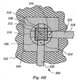
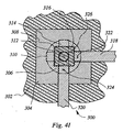
- the fabrication process for embodiment 300 is illustrated in FIGS. 4A-4I, and the feature numbering in FIG. 3 corresponds to the feature numbering in FIGS. 4A-4I.
- the hatching patterns of the various layers in FIG. 3 correspond to the hatching patterns of the various layers in FIGS. 4A-4I.
- embodiment 300 comprises a nanopore 308 that is wide near its second end and narrow near its first end.
- Substrate 306 comprises a region of a material such as silicon dioxide
- the second ring-shaped electrode 310 comprises a conductor such as platinum.
- Second electrode 310 is formed adjacent to the nanopore 308 in a manner that surrounds the perimeter of nanopore 308.
- a first insulator 312 is formed adjacent to the nanopore 308 in a manner that surrounds the perimeter of nanopore 308 and leaves exposed a perimeter portion 330 of second electrode 310.
- a first electrode 314 is formed adjacent to the nanopore 308 in a manner that surrounds the perimeter of nanopore 308.
- first electrode 314 On top of first electrode 314 is optional insulator 316.
- Optional insulator 316 is formed adjacent to the nanopore 308 and is placed in a manner that surrounds the perimeter of nanopore 308 and leaves exposed a perimeter portion 332 of first electrode 314.
- Hole 326 in primary insulator 328 provides access to the first end of the nanopore for a biopolymer molecule 334 represented schematically as a string of beads.
- a voltage source applies a time-varying potential difference between electrodes 310 and 314, via a circuit, not shown, similar to that used for embodiment 100, and the resulting time-varying current is measured by a current measuring means, not shown, similar to that shown in embodiment 100, in order to characterize that portion of biopolymer molecule 334 which happens to be in the favorable position for resonant tunneling to occur.
- FIG. 3 is drawn to scale except for the width of hole 326 and the thickness of layer 328, both of which are drawn to a greatly reduced scale in order to fit them into the drawing.
- FIGS. 4A-4I are drawn to scale except that the diameter of the nanopore 308 is greatly exaggerated to make it visible at the drawing scale.
- FIGS. 5A-5D are not drawn to scale.
- Fabrication begins by forming in a substrate 302 a composite window 304 comprising a layer of silicon nitride typically 200 nm thick on top of a layer of silicon dioxide typically 500 nm thick, both layers forming a cladding layer on the exterior surfaces of a silicon wafer.
- the fabrication of this window 304 is accomplished by the well-known steps of photolithography and etching of a hole in a silicon nitride layer on the bottom side of a substrate 302 such as a wafer of silicon, followed by etching of the substrate 302 in a hot aqueous caustic solution such as tetramethyl ammonium hydroxide (TMAH) in water.
- TMAH tetramethyl ammonium hydroxide
- the caustic etching process removes the silicon beneath the window 304 but leaves the silicon dioxide and silicon nitride layers, resulting in the layout structure illustrated in FIG. 4A.
- Window 304 as drawn is 40 micrometers ( ⁇ m) on a side, but may be larger or smaller.
- a photolithography step is performed to open a window in photoresist, and the silicon nitride layer is etched away to leave silicon dioxide window 306 as illustrated in FIG. 4B.
- This etching step is performed using well-known plasma etching techniques employing carbon tetrafluoride (CF 4 ), oxygen, and nitrogen to achieve a much faster etch rate for silicon nitride than for silicon dioxide.
- CF 4 carbon tetrafluoride
- the technique of fabricating a silicon dioxide window region within a larger window region of silicon nitride on silicon dioxide is a separate invention, useful for obtaining a small, well-supported region of silicon dioxide with advantageous wetting properties as compared to silicon nitride.
- FIB focused ion beam
- This FIB drilling process is followed by a published process of ion beam sculpting using a low energy beam of argon ions which acts to reduce the diameter of the edge of the nanoscale hole near proximate to the ion beam.
- This process is monitored by monitoring current of argon ions through the nanoscale hole, and is terminated when it has resulted in a nanopore 308 with a nominal diameter of 12 nm, as illustrated in FIG. 4C.
- FIG. 5A depicts an example of substrate 302 supporting multiple instances of oxide window 306 surrounding multiple instances of nanopore 308.
- Substrate 302 is tilted at an angle 502 so that its surface is, for example, 45 degrees from horizontal, and is rotated in a direction 504.
- Deposition source 506 a typically a vacuum evaporation source or a molecular beam epitaxy source or a sputtering source, and deposition stream 508 has some angular dispersion 510 as it travels along an average deposition path length 512.
- the result of the tilt and the rotation is that the deposited layer resulting from deposition stream 508 overhangs the edge of nanopore 308 at region 332 shown in FIG. 3.
- the thickness of the layer deposited as shown in FIG. 5A is typically 2 nm, and the deposited material is typically platinum.
- a lithography step is performed, and etching is performed in a dilute solution of aqua regia, comprising a mixture of hydrochloric acid and nitric acid, to define the lateral extent of the second electrode 310 as illustrated in FIG. 4D.
- the electrode 310 is 5 ⁇ m wide.
- a second angled line-of-sight deposition is performed as illustrated in FIG. 5B to form an insulating layer that will comprise optional insulator 312.
- Angle 514 is less than angle 502, for example 35 degrees
- source 516 is typically a molecular beam epitaxy source or a sputtering source.
- the result of the deposition step of FIG. 5B is an insulator layer, typically silicon dioxide, typically 2 nm thick, which overhangs the edge of nanopore 308 but which, as illustrated in FIG. 3, does not occlude the overhanging perimeter 330 of second electrode 310 because perimeter 330 is shadowed from the deposition stream during the line-of-sight deposition.
- a lithography step is performed and etching is performed in a dilute solution of buffered hydrofluouric acid called "buffered oxide etch" or "B.O.E,” to define the lateral extent of optional insulator 312 as shown in FIG. 4E.
- buffered hydrofluouric acid called "buffered oxide etch" or "B.O.E”
- first electrode 314 is similar to the fabrication of second electrode 310.
- a conducting layer typically comprising a 2 nm thickness of platinum, is formed by angled deposition as illustrated in FIG. 5C. Angle 518 is less than angle 514, for example 25 degrees, and source 520 is typically a vacuum evaporation source or a molecular beam epitaxy source or a sputtering source.
- the result of this deposition step is a layer typically 2 nm thick, typically platinum, which overhangs the edge of nanopore 308 at region 332 as illustrated in FIG. 3.
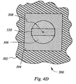
- Lithography and etching define the lateral extent of first electrode 314 as illustrated in FIG. 4F.
- first insulator 316 is similar to fabrication of optional insulator 312.
- An insulating layer is formed by angled deposition as illustrated in FIG. 5D. Angle 522 is less than angle 518, for example 15 degrees.
- Source 524 is typically a molecular beam epitaxy source or a sputtering source. The result of this deposition process is a layer typically 2 nm thick, typically platinum, which overhangs the edge of nanopore 308 but which, as illustrated in FIG. 3, does not occlude overhanging perimeter 332 of first electrode 314 because perimeter 332 is shadowed from the deposition stream during the line-of-sight deposition.
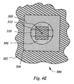
- the lateral extent of first insulator is defined by lithography and etching as illustrated in FIG. 4G.
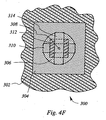
- electrical lead regions 318 and 320 are contacted to the second and first electrode regions 310 and 314 at contact regions 322 and 324.
- Leads 318 and 320 are formed by standard IC techniques of metal deposition and lithography, for example by electron beam deposition of an aluminum layer followed by lithography and etching. Leads 318 and 320 may extend to contact pads, not shown, which provide for electrical contact to a circuit, not shown, similar to the circuit depicted for embodiment 100.
- a insulator layer 328 is formed, for example by spinning on a layer of a polyimide precursor and curing that precursor to form layer of polyimide insulator, in order to provide electrical insulation over leads 318 and 320 and over the ends of electrodes 310 and 314.
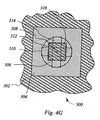
- lithography is performed to open hole 326 depicted in FIG. 3 and FIG. 4I, and to open contact regions over electrical contact pads, not shown.
- the substrate 302 can then be diced by sawing to form individual nanopore chips, not shown, the nanopore chips can be connected to a fluidic apparatus to wet the first and second surfaces of the nanopore, and electrical connection of these chips to an electrical circuit can be performed.
- the above fabrication process produces a series of edges of nanopore 308 defining a portion of the nanopore with successively smaller diameters.
- Each edge has an overhanging region, which can also be called a cornice, the bottom side of which is shadowed from a subsequent line-of-sight deposition so that it remains free of deposits, or nearly so.
- the nanopore 308 when first formed in window 306 has a fourth edge with a fourth portion of the nanopore 308 extending there through.
- the second electrode 310 overhangs the fourth edge, forming a third edge with a third portion of the nanopore 308 extending there through.
- the third portion of the nanopore is smaller than the fourth portion of the nanopore.
- the first insulator 312 overhangs the third edge, forming a first insulator edge with a second portion of the nanopore extending there through.
- the second portion of the nanopore is smaller than the third portion of the nanopore.
- the first electrode 314 overhangs the first insulator edge, forming a first electrode edge with a first portion of the nanopore being smaller than the second portion of the nanopore.
- the optional first insulator 316 overhangs the first electrode edge, forming a insulator edge with a portion of the nanopore smaller than the first portion of the nanopore.
- the initial diameter of the nanopore at window 306 is roughly 12 nm
- the final diameter of the nanopore at first insulator 316 is 2 nm. It will be appreciated that these dimensions are representative only by way of example, and that larger and smaller nanopores can be formed by varying the diameter of the edges, the thickness and number of deposited layers, and the angles of the successive depositions.
- FIG. 3 can equally well be taken to represent a cross section through two adjacent linear edges extending into the plane of the drawing, and the fabrication method discussed above can be used to create two closely spaced line electrodes on each of the two linear edges.
- the left or the right linear edge could be absent from such a structure, leaving two closely spaced line electrodes on a single edge.
- Such closely spaced electrodes can have utility in a number of applications known to those skilled in various arts.
- the means of line-of sight deposition chosen for any of the steps described above, in which case there may be some undesired deposition of insulator material onto electrode region 330 or 332 or both.
- known techniques for removal include, but are not limited to, chemical etching, ion beam milling, sputtering, plasma etching, and reactive ion etching.
- FIG. 6 illustrates an embodiment 600 of the present invention. All of the features numbered in FIG. 6 correspond to the features in FIG. 1, except that each label is incremented by five hundred (500) in comparison to the labels in FIG. 1.
- Embodiment 600 is different from embodiment 100 in that electrodes 616 and 618 are both situated on the first surface of substrate 604, and there is no second electrode situated on second surface 608 of substrate 604. Bead 630 may be in a favorable position between electrodes 616 and 618 for resonant tunneling to occur. However, because embodiment 600 does not have the advantageous ring electrode structure 116 and 118 of embodiment 100, it is less likely that the favorable conditions for resonant tunneling will occur, Thus ring electrode structure similar to those of embodiments 110, 200, and 300 are preferred.
Abstract
Description
- This Nonprovisional Application for Patent is a Continuation-in-Part of U.S. Nonprovisional Application Serial No. 10/352,675, which was filed on January 27, 2003. U.S. Nonprovisional Application for Patent Serial No. 10/352,675 is also hereby incorporated by reference in its entirety.
- The invention relates generally to the field of biopolymers and more particularly to an apparatus and method for characterizing biopolymer molecules.
- Techniques for manipulating matter at the nanometer scale ("nanoscale") are important for many electronic, chemical and biological purposes (See Li et al., "Ion beam sculpting at nanometer length scales", Nature, 412: 166-169, 2001). Among such purposes are the desire to more quickly sequence biopolymers such as DNA. Nanopores, both naturally occurring and artificially fabricated, have recently attracted the interest to molecular biologists and biochemists for the purpose of DNA sequencing.
- It has been demonstrated that a voltage gradient can drive a biopolymer such as single-stranded DNA (ssDNA) in an aqueous ionic solution through a naturally-occurring transsubstrate channel, or "nanopore," such as an α-hemolysin pore in a edgeid bilayer. (See Kasianowicz et al., "Characterization of individual polynucleotide molecules using a substrate channel", Proc. Natl. Acad. Sci. USA, 93: 13770-13773, 1996). The process in which the DNA molecule goes through the pore has been dubbed ''translocation''. During the translocation process, the extended biopolymer molecule blocks a substantial portion of the otherwise open nanopore channel. This blockage decreases the ionic electrical current flow occurring through the nanopore in the ionic solution. The passage of a single biopolymer molecule can therefore be monitored by recording the translocation duration and the decrease in current. Many such events occurring sequentially through a single nanopore provide data that can be plotted to yield useful information concerning the structure of the biopolymer molecule. For example, given uniformly controlled translocation conditions, the length of the individual biopolymer can be estimated from the translocation time.
- One desire of scientists is that the individual monomers of the biopolymer strand might be identified via the characteristics of the blockage current, but this hope may be unrealized because of first-principle signal-to-noise limitations and because the naturally occurring nanopore is thick enough that several monomers of the biopolymer are present in the nanopore simultaneously.
- More recent research has focused on fabricating artificial nanopores. Ion beam sculpting using a diffuse beam of low-energy argon ions has been used to fabricate nanopores in thin insulating substrates of materials such as silicon nitride (See Li et al., "Ion beam sculpting at nanometer length scales", Nature, 412: 166-169,2001). Doublestranded DNA (dsDNA) has been passed through these artificial nanopores in a manner similar to that used to pass ssDNA through naturally occurring nanopores. Current blockage data obtained with dsDNA is reminiscent of ionic current blockages observed when ssDNA is translocated through the channel formed by α-hemolysin in a edgeid bilayer. The duration of these blockages is been on the millisecond scale and current reductions have been to 88% of the open-pore value. This is commensurate with translocation of a rod-like molecule whose cross-sectional area is 3-4 nm2 (See Li et al., "Ion beam sculpting at nanometer length scales", Nature, 412: 166-169,2001). However, as is the case with single-stranded biopolymers passing through naturally occurring nanopores, first-principle signal-to-noise considerations make it difficult or impossible to obtain information on the individual monomers in the biopolymer.
- A second approach has been suggested for detecting a biopolymer translocating a nanopore in a rigid substrate material such as Si3N4. This approach entails placing two tunneling electrodes at the periphery of one end of the nanopore and monitoring tunneling current from one electrode, across the biopolymer, to the other electrode. However, it is well known that the tunneling current has an exponential dependence upon the height and width of the quantum mechanical potential barrier to the tunneling process. This dependence implies an extreme sensitivity to the precise location in the nanopore of the translocating molecule. Both steric attributes and physical proximity to the tunneling electrode could cause changes in the magnitude of the tunneling current which would be far in excess of the innate differences expected between different monomers under ideal conditions. For this reason, it is difficult to expect this simple tunneling configuration to provide the specificity required to perform biopolymer sequencing.
- Resonant tunneling effects have been employed in various semiconductor devices including diodes and transistors. For instance, U.S. Patent 5,504,347, Javanovic, et al., discloses a lateral tunneling diode having gated electrodes aligned with a tunneling barrier. The band structures for a resonant tunneling diode are described wherein a quantum dot is situated between two conductors, with symmetrical quantum barriers on either side of the quantum dot. The resonant tunneling diode may be biased at a voltage level whereby an energy level in the quantum dot matches the conduction band energy in one of the conductors. In this situation the tunneling current between the two conductors versus applied voltage is at a local maximum. At some other bias voltage level, no energy level in the quantum dot matches the conduction band energy in either of the conductors and the current versus applied voltage is at a local minimum. The resonant tunneling diode structure can thus be used to sense the band structure of energy levels within the quantum dot via the method of applying different voltage biases and sensing the resulting current levels at each of the different voltage biases. The different applied voltage biases can form a continuous sweep of voltage levels, and the sensed resulting current levels can form a continuous sweep of current levels. The slope of the current versus voltage can in some cases be negative. Conceptually, it is also possible to inject a known current between the conductors and measure the resulting voltage, but this approach can fail if the characteristic current versus voltage has a negative slope region. For this reason, applying a known voltage bias and sensing the resultant current is usually the preferred method.
- As discussed in Nonprovisional Application Serial No. 10/352,675 referenced above, a resonant tunneling electrode arrangement can be associated with a nanopore so as to sense the presence, and energy band properties of, a biopolymer molecule extending through the nanopore. This resonant tunneling electrode arrangement provides hope of not only sensing or characterizing a biopolymer, but of identifying the constituents of the polymer and meeting the goal of rapid and efficient DNA sequencing.
- Thus there is a need for specific resonant tunneling electrode structures to be associated in such an arrangement with the nanopore in order to characterize biopolymers such as DNA, a method of using such resonant tunneling electrode structures to characterize biopolymers, and methods of building such resonant tunneling electrode structures. The references cited in this application infra and supra, are hereby incorporated in this application by reference. However, cited references or art are not admitted to be prior art to this application.
- The invention provides an apparatus and method for improved detection and characterization of a nanoscale moiety such as a biopolymer. The invention provides a nanopore structure for sensing a nanoscale moiety. The nanopore structure comprises a first electrode, a first insulator and a second electrode. The first electrode has a first portion of a nanopore extending there through and exposing a first electrode edge. A first insulator is adjacent to the first electrode and has a second portion of the nanopore there through and defines a first insulator edge. The first electrode edge overhangs the first insulator edge. A second electrode is adjacent to the first insulator. The second electrode has a third portion of the nanopore there through and defines a second electrode edge. The first insulator edge overhangs the second electrode edge and the first electrode and second electrode may be electrically ramped for sensing the nanoscale moiety. The invention also provides a method of fabricating a nanopore structure with nanopore for sensing a portion of a nanoscale moiety.
- The method of fabrication comprises providing an electrode having a portion of a nanopore there through, the portion of the nanopore defining an electrode edge, depositing an insulator on the electrode adjacent to the nanopore, the insulator having a portion of the nanopore there through and defining an insulator edge, the insulator edge overhanging the electrode edge and depositing an electrode on the insulator adjacent to the nanopore, the electrode having a portion of the nanopore there through and defining an electrode edge, the electrode edge overhanging the insulator edge to define the nanopore structure, wherein the electrodes may be electrically ramped to sense a portion of a nanoscale moiety.
- The invention is described in detail below with reference to the following figures:
- FIG. 1 illustrates a schematic representation of an
embodiment 100 of the present invention. - FIG. 2 illustrates a schematic representation of an
embodiment 200 of the present invention. - FIG. 3 illustrates a cross-sectional detail of an
embodiment 300 of the present invention. - FIGS. 4A-4I illustrate sequential steps of a method of construction of
embodiment 300. - FIGS. 5A-5D illustrate the method of sequential angled line-of sight layer
deposition used in constructing
embodiment 300. - FIG. 6 illustrates an
embodiment 600 of the present invention. -
- This invention is not limited to specific compositions, methods, steps, or equipment, as such may vary. The terminology used herein is for the purpose of describing particular embodiments only, and is not intended to be limiting. Methods recited herein may be carried out in any order of the recited events that is logically possible, as well as the recited order of events. Furthermore, where a range of values is provided, it is understood that every intervening value, between the first and second limit of that range and any other stated or intervening value in that stated range is encompassed within the invention. Also, it is contemplated that any optional feature of the inventive variations described may be set forth and claimed independently, or in combination with any one or more of the features described herein.
- Unless defined otherwise below, all technical and scientific terms used herein have the same meaning as commonly understood by one of ordinary skill in the art to which this invention belongs. Still, certain elements are defined herein for the sake of clarity. In the event that terms in this application are in conflict with the usage of ordinary skill in the art, the usage herein shall be controlling.
- Where a range of values is provided, it is understood that each intervening value, to the tenth of the unit of the second limit unless the context clearly dictates otherwise, between the first and second limit of that range, and any other stated or intervening value in that stated range, is encompassed within the invention. The first and second limits of these smaller ranges may independently be included in the smaller ranges, and are also encompassed within the invention, subject to any specifically excluded limit in the stated range. Where the stated range includes one or both of the limits, ranges excluding either or both of those included limits are also included in the invention.
- As used in this specification and the appended claims, the singular forms "a", "an" and "the" include plural referents unless the context clearly dictates otherwise. Thus, for example, reference to "a biopolymer" includes more than one biopolymer, and reference to "a voltage source " includes a plurality of voltage sources and the like. In describing and claiming the present invention, the following terminology will be used in accordance with the definitions set out below.
- A "biopolymer" is a polymer of one or more types of repeating units. Biopolymers are typically found in biological systems and particularly include polysaccharides (such as carbohydrates), peptides (which term is used to include polypeptides and proteins), glycans, proteoglycans, edgeids, sphingoedgeids, known biologicals materials such as antibodies, etc., and polynucleotides as well as their analogs such as those compounds composed of or containing amino acid analogs or non-amino acid groups, or nucleotide analogs or non-nucleotide groups. This includes polynucleotides in which the conventional backbone has been replaced with a non-naturally occurring or synthetic backbone, and nucleic acids (or synthetic or naturally occurring analogs) in which one or more of the conventional bases has been replaced with a group (natural or synthetic) capable of participating in hydrogen bonding interactions, such as Watson-Crick type, Wobble type and the like. Polynucleotides include single or multiple stranded configurations, where one or more of the strands may or may not be completely aligned with another. A "nucleotide" refers to a sub-unit of a nucleic acid and has a phosphate group, a 5 carbon sugar and a nitrogen containing base, as well as functional analogs (whether synthetic or naturally occurring) of such sub-units which in the polymer form (as a polynucleotide) can hybridize with naturally occurring polynucleotides in a sequence specific manner analogous to that of two naturally occurring polynucleotides. Biopolymers include DNA (including cDNA), RNA, oligonucleotides, and PNA and other polynucleotides as described in U.S. Patent No. 5,948,902 and references cited therein (all of which are also incorporated herein by reference), regardless of the source. An "oligonucleotide" generally refers to a nucleotide multimer of about 10 to 100 nucleotides in length, while a "polynucleotide" includes a nucleotide multimer having any number of nucleotides. A "biomonomer" references a single unit, which can be linked with the same or other biomonomers to form a biopolymer (e.g., a single amino acid or nucleotide with two linking groups one or both of which may have removable protecting groups).
- A "substrate" refers to any surface that may or may not be solid and which is capable of holding, embedding, attaching or which may comprise the whole or portions of an electrode.
- "Hybridizing", "annealing" and "binding", with respect to polynucleotides, are used interchangeably. "Binding efficiency" refers to the productivity of a binding reaction, measured as either the absolute or relative yield of binding product formed under a given set of conditions in a given amount of time. "Hybridization efficiency" is a particular sub-class of binding efficiency, and refers to binding efficiency in the case where the binding components are polynucleotides.
- It will also be appreciated that throughout the present application, that words such as "first", "second" are used in a relative sense only. A "set" may have one type of member or multiple different types. "Fluid" is used herein to reference a liquid.
- The term "tunneling" refers to the change of a particle from a first position in space to a second position in space across an energy barrier region via quantum mechanical tunneling. Typically, the particle may be an electron, and the magnitude of the energy barrier may be defined as the integral of barrier height across a barrier distance.
- The terms "resonance" and "resonant tunneling" refer to a quantum mechanical tunneling effect wherein the energy barriers between each of two current-carrying electrodes and a central potential well are substantially equal in magnitude. This arrangement provides for increased conductivity as compared to non-resonant tunneling across a single energy barrier of the same magnitude as either of the two energy barriers in the resonant tunneling configuration.
- As regards the translocation of a biopolymer through a nanopore, the term "in" refers to being "within" and/or a portion that may also be exterior to. For instance, a biopolymer "in" a nanopore may mean that the whole biopolymer is within the opening of the nanopore or only a small portion of the biopolymer is located near the nanopore with a substantial portion protruding exterior to the nanopore.
- The terms "symmetric" and "symmetrized' refer to the situation in which the tunneling barriers from each electrode to the biopolymer are substantially equal in magnitude.
- The term "nanopore" refers to a pore or hole having a minimum diameter on the order of nanometers and extending through a thin substrate. Nanopores can vary in size and can range from 1 nm to around 300 nm in diameter. Most effective nanopores have been roughly around 1.5nm to 30 nm in diameter. The thickness of the substrate through which the nanopore extends can range from 1 nm to around 700 nm.
- The terms "translocation" and "translocate" refer to movement through a nanopore from one side of the substrate to the other, the movement occurring in a defined direction.
- The terms "portion" and ''portion of a biopolymer" refer to a part, subunit, monomeric unit, portion of a monomeric unit, atom, portion of an atom, cluster of atoms, charge or charged unit.
- The term " time-varying potential" refers to an applied voltage that varies with time. The time-varying potential is produced by the "voltage source".
- The term "voltage difference" refers to an electrical potential difference between any two electrodes.
- The term "adjacent " refers to anything that is near, next to or adjoining. For instance, a nanopore referred to as "adjacent to an electrode" may be near an electrode, it may be next to the electrode, it may pass through an electrode or it may be adjoining the electrode. "Adjacent" can refer to spacing in linear, two-dimensional and three-dimensional space.
- FIG. 1 illustrates a
schematic embodiment 100 of the present invention.Nanopore 102 extends through a section ofoptional substrate 104.Substrate 104 has afirst surface 106 and asecond surface 108.First electrode edge 110 ofnanopore 102 is coincident withfirst surface 106, andsecond electrode edge 112 is coincident withsecond surface 112. Theinterior wall 114 ofnanopore 102 extends through thesubstrate 104. -
First electrode 116 isadjacent nanopore 102, andsecond electrode 118 isadjacent nanopore 102. As illustrated, the interior diameters offirst electrode 116 andsecond electrode 118 are greater than the interior diameter ofwall 114 ofnanopore 102, but this need not be the case, and the interior diameter of eitherelectrode wall 114. -
Electric circuit 120 makes contact tofirst electrode 116 andsecond electrode 118.Electric circuit 120 includes time-varyingvoltage source 122 and current sensing means 124 to sense the resulting current 126. - A nanoscale moiety such as a
biopolymer molecule 128 is schematically depicted as a string of beads with distinct properties threaded throughnanopore 102. Thebiopolymer molecule 128 typically resides in an ionic solvent such as aqueous potassium chloride, not shown, which also extends throughnanopore 102. It should be appreciated that, due to Brownian motion if nothing else,biopolymer molecule 128 is always in motion, and such motion will result in a time-varying position of each bead within thenanopore 102. The motion ofbiopolymer 128 will typically be biased in one direction or another through the pore by providing an external driving force, for example by establishing an electric field through the pore fromfirst electrode edge 110 tosecond electrode edge 112 in the ionic solvent by external means, not shown. -
Bead 130, located near the mid-plane betweenfirst electrode edge 110 andsecond electrode edge 112, may be in a position wherein the magnitude of the quantum mechanical tunneling barrier from itself tofirst electrode 116 is equal to the magnitude of the quantum mechanical tunneling barrier from itself tosecond electrode 118. If it is not in such a favorable position at one instant, the combination of Brownian motion and biased motion will ensure that it has been in such a favorable position immediately beforehand, or that it will be in such a favorable position immediately afterward. In addition, at the instant whenbead 130 is in the desired favorable position, the two beads adjacent to bead 130 will not be in the desired favorable position. Thus, for the instant whenbead 130 is in the favorable position, rapidly varying thevoltage 122 with time and measuring the resulting current 126 provides a measure of the electronic band structure ofbead 130, and of equal importance, does not provide a measure of the electronic band structure of the two beads adjacent to bead 130. Thus the electronic energy band structure ofbead 128 alone can be elucidated for that instant in time. - The use of additional electrodes associated with
nanopore 102 is within the scope of the invention. - The
biopolymer 128 may comprise a variety of shapes, sizes and materials. The shape or size of the molecule is not important, but it must be capable of translocation through thenanopore 102. For instance, both single stranded and double stranded RNA and DNA may be used as abiopolymer 128. In addition, thebiopolymer 128 may contain groups or functional groups that are charged. Furthermore, metals or materials may be added, doped or intercalated within thebiopolymer 128 to provide a net dipole, to provide a net charge, to provide conductivity through the biomolecule or to provide some combination of the above properties. - The
first electrode 116 may comprise a variety of electrically conductive materials. Such materials include electrically conductive metals and alloys of platinum, iridium, rhodium, gold, tin, copper, zinc, iron, magnesium, cobalt, nickel, and vanadium. Other materials well known in the art that provide for electrical conduction may also be employed. When thefirst electrode 116 is deposited on or comprises a portion of thesubstrate 104, it may be positioned in any location relative to thesecond electrode 118 such that a potential can be established between thefirst electrode 116 and thesecond electrode 118. In addition, thebipolymer 128 must be positioned sufficiently close so that a portion of it may be sensed or characterized. In other words, thefirst electrode 116, thesecond electrode 118, and thenanopore 102 must be spaced and positioned in such a way that thebiopolymer 128 may be sensed or characterized. This should not be interpreted to mean that theschematic embodiment 100 shown in Figure 1 in any way limits the scope of the spatial orientation and positioning of each of the components of the invention. Theelectrodes first electrode 116, and thesecond electrode 118 in such a manner that a portion ofbiopolymer 128 in the process of translocating throughpore 102 finds itself in the favorable position wherein resonant tunneling can occur. - The
second electrode 118 may comprise the same or similar materials as described above for thefirst electrode 116. As discussed above, its shape, size and positioning may be altered relative to thefirst electrode 116 and the nanopore 3. - The
optional substrate 104 may comprise a variety of materials known in the art for designing substrates and nanopores.Substrate 104 may comprise one or more layers of one or more materials including, but not limited to, membranes, edgeids, silicon nitride, silicon dioxide, platinum or other metals, silicon oxynitride, silicon rich nitride, organic polymers, and other insulating layers, carbon based materials, plastics, metals, or other materials known in the art for etching or fabricating semiconductor or electrically conducting materials.Substrate 104 need not be of uniform thickness.Substrate 104 may or may not be a solid material, and for example may comprise in part or in whole a edgeid bilayer, a mesh, wire, or other material in which a nanopore may be constructed.Substrate 104 may comprise various shapes and sizes. However, it must be large enough and of sufficient width to be capable of forming thenanopore 102 through it. - The
nanopore 102 may be positioned anywhere on/through thesubstrate 104. Thenanopore 102 may also be established by the spacing between thefirst electrode 116 and the second electrode 118 (in a planar or non planar arrangement). Thenanopore 102 may range in size from 1 nm to as large as 300 nm. In most cases, effective nanopores for sensing or characterizing biopolymers would be in the range of around 2-20 nm. These size nanopores are just large enough to allow for translocation of a biopolymer. Thenanopore 102 may be established using any methods well known in the art. For instance, thenanopore 102 may be sculpted in thesubstrate 104 by means of low-energy argon ion beam sculpting of an initially larger hole formed by etching or focused ion beam machining, or by sputtering, etching, photolithography, or other methods and techniques well known in the art. - The
voltage source 122 may be positioned anywhere relative to thesubstrate 104, thenanopore 102, thefirst electrode 116 and thesecond electrode 118. Thevoltage source 122 should be capable of establishing a time-varying voltage difference between thefirst electrode 116 and thesecond electrode 118. A variety ofvoltage sources 122 may be employed consistent with the present invention. A number of these voltage sources are known in the art. - FIG. 2 illustrates a
schematic embodiment 200 of the present invention. All of the features numbered in FIG. 2 correspond to the features in FIG. 1, except that each label is incremented by one hundred (100) in comparison to the labels in FIG. 1. The drawing presents a cutaway view of the nanopore.Embodiment 200 is different fromembodiment 100 in thatelectrodes interior wall 214 ofnanopore 202, and there is no second electrode situated onsecond surface 208 ofsubstrate 204.Bead 230 may be in a favorable position betweenelectrodes electrodes electrodes electrodes electrodes embodiment 200 offers the possibility of better sensing of the properties ofbiopolymer molecule 228 thanembodiment 100 offers formolecule 128. - Although FIG. 1 and FIG. 2 each show a pair of electrodes, the invention should not be interpreted to be limited to only this two-electrode configuration. Various electrodes of varying shapes or sizes may be employed. Furthermore, it is anticipated that the invention comprises a number of similar or different electrodes capable of tunneling in a variety of directions and space (i.e. one, two and three dimensional space).
- FIG. 3 illustrates a cross-sectional detail of an
embodiment 300 of the present invention.Embodiment 300 is an embodiment in which the desired advantageous ring-shaped electrode structures ofembodiment 200 are implemented. The fabrication process forembodiment 300 is illustrated in FIGS. 4A-4I, and the feature numbering in FIG. 3 corresponds to the feature numbering in FIGS. 4A-4I. In addition, the hatching patterns of the various layers in FIG. 3 correspond to the hatching patterns of the various layers in FIGS. 4A-4I. - As seen in FIG. 3,
embodiment 300 comprises ananopore 308 that is wide near its second end and narrow near its first end.Substrate 306 comprises a region of a material such as silicon dioxide, and the second ring-shapedelectrode 310 comprises a conductor such as platinum.Second electrode 310 is formed adjacent to thenanopore 308 in a manner that surrounds the perimeter ofnanopore 308. On top of second electrode 310 afirst insulator 312 is formed adjacent to thenanopore 308 in a manner that surrounds the perimeter ofnanopore 308 and leaves exposed aperimeter portion 330 ofsecond electrode 310. On top offirst insulator 312, afirst electrode 314 is formed adjacent to thenanopore 308 in a manner that surrounds the perimeter ofnanopore 308. On top offirst electrode 314 isoptional insulator 316.Optional insulator 316 is formed adjacent to thenanopore 308 and is placed in a manner that surrounds the perimeter ofnanopore 308 and leaves exposed aperimeter portion 332 offirst electrode 314.Hole 326 inprimary insulator 328 provides access to the first end of the nanopore for abiopolymer molecule 334 represented schematically as a string of beads. - One particular point along the
biopolymer 334 represented asbead 336 is shown in a favorable position for resonant tunneling to occur. A voltage source, not shown, applies a time-varying potential difference betweenelectrodes embodiment 100, and the resulting time-varying current is measured by a current measuring means, not shown, similar to that shown inembodiment 100, in order to characterize that portion ofbiopolymer molecule 334 which happens to be in the favorable position for resonant tunneling to occur. - The method of fabrication of
embodiment 300 is described as follows with reference to FIGS. 3, 4A-4I, and 5A-5D. FIG. 3 is drawn to scale except for the width ofhole 326 and the thickness oflayer 328, both of which are drawn to a greatly reduced scale in order to fit them into the drawing. FIGS. 4A-4I are drawn to scale except that the diameter of thenanopore 308 is greatly exaggerated to make it visible at the drawing scale. FIGS. 5A-5D are not drawn to scale. - Fabrication begins by forming in a substrate 302 a
composite window 304 comprising a layer of silicon nitride typically 200 nm thick on top of a layer of silicon dioxide typically 500 nm thick, both layers forming a cladding layer on the exterior surfaces of a silicon wafer. The fabrication of thiswindow 304 is accomplished by the well-known steps of photolithography and etching of a hole in a silicon nitride layer on the bottom side of asubstrate 302 such as a wafer of silicon, followed by etching of thesubstrate 302 in a hot aqueous caustic solution such as tetramethyl ammonium hydroxide (TMAH) in water. The caustic etching process removes the silicon beneath thewindow 304 but leaves the silicon dioxide and silicon nitride layers, resulting in the layout structure illustrated in FIG. 4A.Window 304 as drawn is 40 micrometers (µm) on a side, but may be larger or smaller. - Next a photolithography step is performed to open a window in photoresist, and the silicon nitride layer is etched away to leave
silicon dioxide window 306 as illustrated in FIG. 4B. This etching step is performed using well-known plasma etching techniques employing carbon tetrafluoride (CF4), oxygen, and nitrogen to achieve a much faster etch rate for silicon nitride than for silicon dioxide. The technique of fabricating a silicon dioxide window region within a larger window region of silicon nitride on silicon dioxide is a separate invention, useful for obtaining a small, well-supported region of silicon dioxide with advantageous wetting properties as compared to silicon nitride. - Next, drilling is performed in the center of
window 306 using a focused ion beam (FIB) of gallium ions, resulting in a nanoscale hole with a diameter on the order of 50-100 nm extending through the thickness of the silicon dioxide layer. This FIB drilling process is followed by a published process of ion beam sculpting using a low energy beam of argon ions which acts to reduce the diameter of the edge of the nanoscale hole near proximate to the ion beam. This process is monitored by monitoring current of argon ions through the nanoscale hole, and is terminated when it has resulted in ananopore 308 with a nominal diameter of 12 nm, as illustrated in FIG. 4C. - Next, a process of angled line-of-sight deposition as illustrated in FIG. 5A is used to deposit a layer of material used to form
second electrode 310. FIG. 5A depicts an example ofsubstrate 302 supporting multiple instances ofoxide window 306 surrounding multiple instances ofnanopore 308.Substrate 302 is tilted at anangle 502 so that its surface is, for example, 45 degrees from horizontal, and is rotated in adirection 504. Deposition source 506 a typically a vacuum evaporation source or a molecular beam epitaxy source or a sputtering source, anddeposition stream 508 has someangular dispersion 510 as it travels along an averagedeposition path length 512. The result of the tilt and the rotation is that the deposited layer resulting fromdeposition stream 508 overhangs the edge ofnanopore 308 atregion 332 shown in FIG. 3. The thickness of the layer deposited as shown in FIG. 5A is typically 2 nm, and the deposited material is typically platinum. - Next, a lithography step is performed, and etching is performed in a dilute solution of aqua regia, comprising a mixture of hydrochloric acid and nitric acid, to define the lateral extent of the
second electrode 310 as illustrated in FIG. 4D. As drawn theelectrode 310 is 5 µm wide. - Next, a second angled line-of-sight deposition is performed as illustrated in FIG. 5B to form an insulating layer that will comprise
optional insulator 312.Angle 514 is less thanangle 502, for example 35 degrees, andsource 516 is typically a molecular beam epitaxy source or a sputtering source. The result of the deposition step of FIG. 5B is an insulator layer, typically silicon dioxide, typically 2 nm thick, which overhangs the edge ofnanopore 308 but which, as illustrated in FIG. 3, does not occlude the overhangingperimeter 330 ofsecond electrode 310 becauseperimeter 330 is shadowed from the deposition stream during the line-of-sight deposition. - Next, a lithography step is performed and etching is performed in a dilute solution of buffered hydrofluouric acid called "buffered oxide etch" or "B.O.E," to define the lateral extent of
optional insulator 312 as shown in FIG. 4E. - Fabrication of
first electrode 314 is similar to the fabrication ofsecond electrode 310. A conducting layer, typically comprising a 2 nm thickness of platinum, is formed by angled deposition as illustrated in FIG. 5C.Angle 518 is less thanangle 514, for example 25 degrees, andsource 520 is typically a vacuum evaporation source or a molecular beam epitaxy source or a sputtering source. The result of this deposition step is a layer typically 2 nm thick, typically platinum, which overhangs the edge ofnanopore 308 atregion 332 as illustrated in FIG. 3. Lithography and etching define the lateral extent offirst electrode 314 as illustrated in FIG. 4F. - Fabrication of
first insulator 316 is similar to fabrication ofoptional insulator 312. An insulating layer is formed by angled deposition as illustrated in FIG. 5D.Angle 522 is less thanangle 518, for example 15 degrees.Source 524 is typically a molecular beam epitaxy source or a sputtering source. The result of this deposition process is a layer typically 2 nm thick, typically platinum, which overhangs the edge ofnanopore 308 but which, as illustrated in FIG. 3, does not occlude overhangingperimeter 332 offirst electrode 314 becauseperimeter 332 is shadowed from the deposition stream during the line-of-sight deposition. The lateral extent of first insulator is defined by lithography and etching as illustrated in FIG. 4G. - Next, as illustrated in FIG. 4H,
electrical lead regions first electrode regions contact regions Leads Leads embodiment 100. - Next a
insulator layer 328 is formed, for example by spinning on a layer of a polyimide precursor and curing that precursor to form layer of polyimide insulator, in order to provide electrical insulation over leads 318 and 320 and over the ends ofelectrodes nanopore 328, lithography is performed to openhole 326 depicted in FIG. 3 and FIG. 4I, and to open contact regions over electrical contact pads, not shown. - The
substrate 302 can then be diced by sawing to form individual nanopore chips, not shown, the nanopore chips can be connected to a fluidic apparatus to wet the first and second surfaces of the nanopore, and electrical connection of these chips to an electrical circuit can be performed. - It will be appreciated that the above fabrication process produces a series of edges of
nanopore 308 defining a portion of the nanopore with successively smaller diameters. Each edge has an overhanging region, which can also be called a cornice, the bottom side of which is shadowed from a subsequent line-of-sight deposition so that it remains free of deposits, or nearly so. Thus, thenanopore 308 when first formed inwindow 306 has a fourth edge with a fourth portion of thenanopore 308 extending there through. Thesecond electrode 310 overhangs the fourth edge, forming a third edge with a third portion of thenanopore 308 extending there through. The third portion of the nanopore is smaller than the fourth portion of the nanopore. Thefirst insulator 312 overhangs the third edge, forming a first insulator edge with a second portion of the nanopore extending there through. The second portion of the nanopore is smaller than the third portion of the nanopore. Thefirst electrode 314 overhangs the first insulator edge, forming a first electrode edge with a first portion of the nanopore being smaller than the second portion of the nanopore. The optionalfirst insulator 316 overhangs the first electrode edge, forming a insulator edge with a portion of the nanopore smaller than the first portion of the nanopore. Thus, beginning with a nanopore of initially large diameter and using the techniques of successive angled line-of-sight depositions, it is possible to end with a nanopore of small diameter. As drawn in FIG. 3, the initial diameter of the nanopore atwindow 306 is roughly 12 nm, and the final diameter of the nanopore atfirst insulator 316 is 2 nm. It will be appreciated that these dimensions are representative only by way of example, and that larger and smaller nanopores can be formed by varying the diameter of the edges, the thickness and number of deposited layers, and the angles of the successive depositions. - It will be appreciated that the particular details of the above structures and fabrication processes are representative only by way of example, and are in no way intended to be limiting. Many variations in structures and materials will occur to those skilled in the art without departing from the scope and spirit of the present invention. Additional layers may be added to the nanopore structure by the obvious extension of the techniques presented herein without departing from the scope and spirit of the present invention.
- It will be appreciated that the utility of the structures and processes described herein has been discussed with respect to the theory of resonant tunneling, but that the utility of these structures and processes is in no way limited to resonant tunneling, but instead applies also to other physical phenomena useful for measurement and manipulation of small object including biopolymers, including but not limited to non-resonant tunneling, electrostatic attraction and repulsion, fluidic field effect transistors, electrolysis, and the like. Either one or both of
electrodes insulator 312 betweenelectrodes - It will be appreciated that the electrode structures and fabrication techniques described herein have been presented with reference to the nanoscale, but that they may also possess utility at the larger microscale wherein the thicknesses of various layers are in the range of 100 nm to 25 µm.
- It will be appreciated that the method of fabrication discussed above has been discussed with reference to a nanopore having a cross section similar to that in FIG. 3. However, the fabrication process is not restricted to nanopores. FIG. 3 can equally well be taken to represent a cross section through two adjacent linear edges extending into the plane of the drawing, and the fabrication method discussed above can be used to create two closely spaced line electrodes on each of the two linear edges. Likewise, either the left or the right linear edge could be absent from such a structure, leaving two closely spaced line electrodes on a single edge. Such closely spaced electrodes can have utility in a number of applications known to those skilled in various arts.
- It will be appreciated that the means of line-of sight deposition chosen for any of the steps described above, in which case there may be some undesired deposition of insulator material onto
electrode region - FIG. 6 illustrates an
embodiment 600 of the present invention. All of the features numbered in FIG. 6 correspond to the features in FIG. 1, except that each label is incremented by five hundred (500) in comparison to the labels in FIG. 1.Embodiment 600 is different fromembodiment 100 in thatelectrodes second surface 608 of substrate 604.Bead 630 may be in a favorable position betweenelectrodes embodiment 600 does not have the advantageousring electrode structure embodiment 100, it is less likely that the favorable conditions for resonant tunneling will occur, Thus ring electrode structure similar to those ofembodiments
Claims (32)
- A nanopore structure with nanopore (102; 202; 308) for sensing a nonscale moiety, comprising:wherein the first electrode (116; 216; 314) and the second electrode (118; 218; 310) may be electrically ramped for sensing the nanoscale moiety.(a) a first electrode (116; 216; 314) having a first portion of the nanopore (102; 202; 308) extending there through and exposing a first electrode edge;(b) a first insulator adjacent to the first electrode (116; 216; 314), the first insulator having a second portion of the nanopore (102; 202; 308) there through and defining a first insulator edge, the first electrode edge overhanging the first insulator edge;(c) a second electrode (118; 218; 310) adjacent to the first insulator, the second electrode (118; 218; 310) having a third portion of the nanopore (102; 202; 308) there through and defining a second electrode edge, the first insulator edge overhanging the second electrode edge;
- A nanopore structure as recited in claim 1, further comprising a substrate (104; 204; 306) adjacent to the second electrode.
- A nanopore structure as recited in claim 1 or 2, wherein the first electrode edge defines a first diameter portion of the nanopore, and the first insulator edge defines a second diameter portion of the nanopore, the first diameter portion of the nanopore being smaller than the second diameter portion of the nanopore.
- A nanopore structure as recited in any of claims 1 to 3, further comprising an optional insulator (316) contacting the first electrode (314) and being adjacent to the nanopore (308), the optional insulator (316) having a portion of the nanopore there through and defining an insulator edge, the edge overhanging the first electrode edge (314).
- A nanopore structure as recited in claim 4, wherein the edge of the optional insulator (316) defines a diameter portion of the nanopore (308), the diameter portion of the nanopore being smaller than the first diameter portion of the nanopore.
- A nanopore structure as recited in any of claims 1 to 5, wherein the first electrode (116; 216; 314) comprises a ring structure.
- A nanopore structure as recited in any of claims 1 to 6, wherein the second electrode ( 118; 218; 310) comprises a ring structure.
- A nanopore structure as recited in any of claims 1 to 7, wherein both the first electrode (116; 216; 314) and the second electrode (118; 218; 310) comprise a ring structure.
- A nanopore structure (100; 200; 300) as recited in any of claims 1 to 8, further comprising an electric circuit (120; 220).
- A nanopore structure as recited in claim 9, wherein the electric circuit (120; 220) further comprises a voltage source (122; 222) for electrically connecting the first electrode with the second electrode and generating a potential between the first electrode and the second electrode for sensing a nanoscale moiety in the nanopore.
- A nanopore structure as recited in claim 10, wherein the voltage source (122; 222) comprises a time varying voltage source.
- A nanopore structure as recited in any of claims 9 to 11, where the electric circuit (120; 220) further comprises a current sensor (124, 224) for sensing a resulting current.
- A nanopore structure (100; 200; 300) as recited in any of claims 1 to 12, wherein the nanoscale moiety is selected from the group consisting of an ion, a monomer, an atom, a metal, a halide, an amino acid, nucleotide, a simple sugar, a quantum dot, and a nanosphere.
- A nanopore structure as recited in any of claims 1 to 13, wherein the nanoscale moiety comprises a biopolymer (128; 228; 334).
- A nanopore structure as recited in claim 14, wherein the biopolymer is selected from the group consisting of a polypeptide, a polynucleotide, a synthetic polymer, a non synthetic polymer and a polysaccharide.
- A nanopore structure as recited in claim 15, wherein the polynucleotide is selected from the group consisting of deoxyribonucleic acid (DNA), ribonucleic acid (RNA), single stranded DNA, single stranded RNA, double stranded RNA, double stranded DNA, DNA complexed to RNA, DNA bound to protein, RNA bound to protein, transfer RNA (tRNA), and messenger RNA (mRNA).
- A nonopore structure as recited in any of claims 1 to 16, where the first electrode (116; 216; 314) comprises a material selected from the group consisting of platinum iridium, palladium, rhodium, gold, tin, copper, zinc, iron, magnesium, cobalt, nickel, vanadium and their alloys.
- A nanopore structure as recited in any of claims 1 to 17, wherein the second electrode (118; 218; 310) comprises a material selected from the group consisting of platinum, iridium, gold, tin, copper, zinc, iron, magnesium, cobalt, nickel, vanadium and their alloys.
- A nanopore structure as recited in any of claims 1 to 18, wherein the nanopore (102; 202; 308) is from 1 nanometer to 300 nanometers.
- A nanopore structure as recited in any of claims 1 to 19, wherein the first insulator comprises a material selected from the group consisting of silicon dioxide, silicon nitride, oxynitride, platinum oxide, and aluminium oxide.
- A nanopore structure as recited in any of claims 4 to 20, wherein the optional insulator (316) comprises a material selected from the group consisting of silicon dioxide, silicon nitride, oxynitride, platinum oxide, and aluminium oxide.
- A method of fabricating a nanopore structure with nanopore (102; 202; 308) for sensing a portion of a nanoscale moiety, comprising:(a) providing an electrode (116; 216; 314) having a portion of a nanopore (102; 202; 308) there through, the portion of the nanopore defining an electrode edge;(b) depositing an insulator on the electrode (116; 216; 314) adjacent to the nanopore, (102; 202; 308), the insulator having a portion of the nanopore there through and defining an insulator edge, the insulator edge overhanging the electrode edge; and(c) depositing a second electrode (118; 218; 310) on the insulator adjacent to the nanopore (102; 202; 308), the electrode having a portion of the nanopore there through and defining an electrode edge, the electrode edge overhanging the insulator edge to define the nanopore structure;
- A method of fabricating a nanopore structure as recited in claim 22, wherein at least one deposition step is performed by angled line of sight deposition.
- A method of fabricating a nanopore structure as recited in claim 22 or 23, wherein each step is performed by angled line of sight deposition.
- A method for sensing a nanoscale moiety, comprising:(a) providing a nanopore with layered sidewall comprising a conductive region;(b) introducing a nanoscale moiety into the nanopore;(c) sensing the nanoscale moiety by ramping an electric potential at the conductive region.
- A method of making a layered nanopore structure, comprising:(a) providing a substrate (302) with a surface and a portion of a nanopore (308) there through;(b) tilting the substrate surface to an angle (502) defined between horizontal and the substrate surface;(c) rotating the substrate (302) at the tilted angle;(d) depositing a second electrode (310) on the substrate surface adjacent to the nanopore (308) to define a second electrode edge;(e) tilting the substrate surface to an angle (514) defined between the horizontal and the substrate surface;(f) rotating the substrate (302) and second electrode (310) at the tilted angle;(g) depositing a first insulator (312) on the second electrode (310) adjacent to the nanopore (308) to define a first insulator edge;(h) tilting the substrate surface at an angle (518) defined between horizontal and the substrate surface;(i) rotating the substrate (302) at the tilted angle;(j) depositing a first electrode (314) on the substrate surface adjacent to the nanopore (308) to define a first electrode edge wherein the first electrode edge, the first insulator edge and the second electrode edges define a layered nanopore structure.
- A method as recited in claim 26, wherein the angle defined in step (b) is greater than the angle defined in step (e).
- A method as recited in claim 26 or 27, wherein the angle defined in step (e) is greater than the angle defined in step (h).
- A method as recited in any of claims 26 to 28, wherein the angle (502) defined in step (b) is 45 degrees.
- A method as recited in any of claims 26 to 29, wherein the angle (514) defined in step (e) is 35 degrees.
- A method as recited in any of claims 26 to 30, wherein the angle (518) defined in step (h) is 25 degrees.
- A method of making a layered nanopore structure, comprising:(a) etching a silicon substrate (302) to form a window (304) of silicon nitride on silicon dioxide;(b) etching the silicon nitride to form a window (306) of silicon dioxide;(c) forming a nanopore (308) using focused ion beam drilling followed by argon ion beam sculpting;(d) depositing a second electrode (310) on the substrate (302) adjacent to the nanopore (308) and defining the second electrode (310) by photolithography;(e) depositing a first insulator (312) on the second electrode (310) adjacent to the nanopore and defining the first insulator layer by photolithography;(f) depositing a first electrode (314) on the first insulator (312) adjacent to the nanopore (308) and defining the first electrode (314) by photolithography;(g) depositing an optional insulator (316) on the second electrode (314) adjacent to the nanopore (308) and defining the optional insulator (316) by photolithography;(h) depositing an aluminium interconnect layer (318, 320) on the optional insulator (316) and defining the aluminium interconnect layer (318, 320) by photolithography; and(i) depositing an insulator substrate (328) on the aluminium interconnect layer (318, 320) and defining the insulator substrate layer (328) by photolithography.
Applications Claiming Priority (2)
| Application Number | Priority Date | Filing Date | Title |
|---|---|---|---|
| US10/462,216 US7250115B2 (en) | 2003-06-12 | 2003-06-12 | Nanopore with resonant tunneling electrodes |
| US462216 | 2003-06-12 |
Publications (1)
| Publication Number | Publication Date |
|---|---|
| EP1486775A1 true EP1486775A1 (en) | 2004-12-15 |
Family
ID=33299921
Family Applications (1)
| Application Number | Title | Priority Date | Filing Date |
|---|---|---|---|
| EP04010944A Withdrawn EP1486775A1 (en) | 2003-06-12 | 2004-05-07 | Nanopore with resonant tunneling electrodes |
Country Status (2)
| Country | Link |
|---|---|
| US (1) | US7250115B2 (en) |
| EP (1) | EP1486775A1 (en) |
Cited By (37)
| Publication number | Priority date | Publication date | Assignee | Title |
|---|---|---|---|---|
| EP1712893A1 (en) * | 2005-04-14 | 2006-10-18 | Agilent Technologies, Inc., A Delaware Corporation | Planar resonant tunneling sensor and method of fabricating and using same |
| EP1712891A2 (en) * | 2005-04-15 | 2006-10-18 | Agilent Technologies, Inc., A Delaware Corporation | Molecular resonant tunneling sensor and methods of fabricating and using the same |
| US7297041B2 (en) * | 2004-10-04 | 2007-11-20 | The Board Of Trustees Of The University Of Illinois | Method of manufacturing microdischarge devices with encapsulated electrodes |
| US7477017B2 (en) | 2005-01-25 | 2009-01-13 | The Board Of Trustees Of The University Of Illinois | AC-excited microcavity discharge device and method |
| WO2009035647A1 (en) * | 2007-09-12 | 2009-03-19 | President And Fellows Of Harvard College | High-resolution molecular graphene sensor comprising an aperture in the graphene layer |
| WO2010111605A3 (en) * | 2009-03-27 | 2010-11-11 | Nabsys, Inc. | Devices and methods for analyzing biomolecules and probes bound thereto |
| US20100310421A1 (en) * | 2009-05-28 | 2010-12-09 | Nabsys, Inc. | Devices and methods for analyzing biomolecules and probes bound thereto |
| US8221179B2 (en) | 2001-10-26 | 2012-07-17 | The Board Of Trustees Of The University Of Illinois | Method of making arrays of thin sheet microdischarge devices |
| US8262879B2 (en) | 2008-09-03 | 2012-09-11 | Nabsys, Inc. | Devices and methods for determining the length of biopolymers and distances between probes bound thereto |
| US8278047B2 (en) | 2007-10-01 | 2012-10-02 | Nabsys, Inc. | Biopolymer sequencing by hybridization of probes to form ternary complexes and variable range alignment |
| US8455260B2 (en) | 2009-03-27 | 2013-06-04 | Massachusetts Institute Of Technology | Tagged-fragment map assembly |
| US8497631B2 (en) | 2006-01-23 | 2013-07-30 | The Board Of Trustees Of The University Of Illinois | Polymer microcavity and microchannel devices and fabrication method |
| US8603303B2 (en) | 2010-03-15 | 2013-12-10 | International Business Machines Corporation | Nanopore based device for cutting long DNA molecules into fragments |
| AU2008236694B2 (en) * | 2007-04-04 | 2014-01-23 | The Regents Of The University Of California | Compositions, devices, systems, and methods for using a nanopore |
| US8669124B2 (en) | 2008-08-20 | 2014-03-11 | Nxp, B.V. | Apparatus and method for molecule detection using nanopores |
| US8715933B2 (en) | 2010-09-27 | 2014-05-06 | Nabsys, Inc. | Assay methods using nicking endonucleases |
| US8764968B2 (en) | 2011-01-28 | 2014-07-01 | International Business Machines Corporation | DNA sequencing using multiple metal layer structure with organic coatings forming transient bonding to DNA bases |
| US8794054B2 (en) | 2009-04-03 | 2014-08-05 | Nxp, B.V. | Sensor device and a method of manufacturing the same |
| US8852407B2 (en) | 2011-01-28 | 2014-10-07 | International Business Machines Corporation | Electron beam sculpting of tunneling junction for nanopore DNA sequencing |
| US8859201B2 (en) | 2010-11-16 | 2014-10-14 | Nabsys, Inc. | Methods for sequencing a biomolecule by detecting relative positions of hybridized probes |
| US8882980B2 (en) | 2008-09-03 | 2014-11-11 | Nabsys, Inc. | Use of longitudinally displaced nanoscale electrodes for voltage sensing of biomolecules and other analytes in fluidic channels |
| US8968668B2 (en) | 2011-06-24 | 2015-03-03 | The Board Of Trustees Of The University Of Illinois | Arrays of metal and metal oxide microplasma devices with defect free oxide |
| US8986524B2 (en) | 2011-01-28 | 2015-03-24 | International Business Machines Corporation | DNA sequence using multiple metal layer structure with different organic coatings forming different transient bondings to DNA |
| US9034637B2 (en) | 2007-04-25 | 2015-05-19 | Nxp, B.V. | Apparatus and method for molecule detection using nanopores |
| US9046511B2 (en) | 2013-04-18 | 2015-06-02 | International Business Machines Corporation | Fabrication of tunneling junction for nanopore DNA sequencing |
| US9097698B2 (en) | 2013-06-19 | 2015-08-04 | International Business Machines Corporation | Nanogap device with capped nanowire structures |
| US9128078B2 (en) | 2013-06-19 | 2015-09-08 | International Business Machines Corporation | Manufacturable sub-3 nanometer palladium gap devices for fixed electrode tunneling recognition |
| US9377437B2 (en) | 2010-02-08 | 2016-06-28 | Genia Technologies, Inc. | Systems and methods for characterizing a molecule |
| US9650668B2 (en) | 2008-09-03 | 2017-05-16 | Nabsys 2.0 Llc | Use of longitudinally displaced nanoscale electrodes for voltage sensing of biomolecules and other analytes in fluidic channels |
| US9914966B1 (en) | 2012-12-20 | 2018-03-13 | Nabsys 2.0 Llc | Apparatus and methods for analysis of biomolecules using high frequency alternating current excitation |
| US10029915B2 (en) | 2012-04-04 | 2018-07-24 | International Business Machines Corporation | Functionally switchable self-assembled coating compound for controlling translocation of molecule through nanopores |
| CN109358106A (en) * | 2018-11-05 | 2019-02-19 | 中国科学院重庆绿色智能技术研究院 | A kind of polysaccharide single molecule structure analytic method based on solid nano hole technology |
| US10294516B2 (en) | 2013-01-18 | 2019-05-21 | Nabsys 2.0 Llc | Enhanced probe binding |
| KR20200042894A (en) * | 2017-06-21 | 2020-04-24 | 온테라 인크. | Dual Pore-Control and Sensing Devices |
| CN113899803A (en) * | 2021-11-09 | 2022-01-07 | 北京航空航天大学 | ISFETs sensing structure with 3D pore channel |
| US11274341B2 (en) | 2011-02-11 | 2022-03-15 | NABsys, 2.0 LLC | Assay methods using DNA binding proteins |
| US11970738B2 (en) | 2020-11-13 | 2024-04-30 | The Regents Of The University Of California | Compositions, devices, systems, and methods for using a nanopore |
Families Citing this family (75)
| Publication number | Priority date | Publication date | Assignee | Title |
|---|---|---|---|---|
| US7692219B1 (en) | 2004-06-25 | 2010-04-06 | University Of Hawaii | Ultrasensitive biosensors |
| JP4608697B2 (en) * | 2004-08-27 | 2011-01-12 | 独立行政法人物質・材料研究機構 | DNA base sequence analysis method and base sequence analysis apparatus using field effect device |
| US20060210995A1 (en) * | 2005-03-15 | 2006-09-21 | Joyce Timothy H | Nanopore analysis systems and methods of using nanopore devices |
| WO2007041621A2 (en) * | 2005-10-03 | 2007-04-12 | Xingsheng Sean Ling | Hybridization assisted nanopore sequencing |
| US7638034B2 (en) | 2006-09-21 | 2009-12-29 | Los Alamos National Security, Llc | Electrochemical detection of single molecules using abiotic nanopores having electrically tunable dimensions |
| US9632073B2 (en) | 2012-04-02 | 2017-04-25 | Lux Bio Group, Inc. | Apparatus and method for molecular separation, purification, and sensing |
| US8592225B2 (en) * | 2006-09-28 | 2013-11-26 | The Board Of Trustees Of The Leland Stanford Junior University | Array-based bioactivated nanopore devices |
| CN101669026B (en) | 2006-12-14 | 2014-05-07 | 生命技术公司 | Methods and apparatus for measuring analytes using large scale FET arrays |
| US8349167B2 (en) | 2006-12-14 | 2013-01-08 | Life Technologies Corporation | Methods and apparatus for detecting molecular interactions using FET arrays |
| US11339430B2 (en) | 2007-07-10 | 2022-05-24 | Life Technologies Corporation | Methods and apparatus for measuring analytes using large scale FET arrays |
| US8262900B2 (en) | 2006-12-14 | 2012-09-11 | Life Technologies Corporation | Methods and apparatus for measuring analytes using large scale FET arrays |
| EP2158476B8 (en) | 2007-05-08 | 2019-10-09 | Trustees of Boston University | Chemical functionalization of solid-state nanopores and nanopore arrays and applications thereof |
| US8349546B2 (en) * | 2007-06-28 | 2013-01-08 | Ming-Nung Lin | Fabricating method of nano-ring structure by nano-lithography |
| CN101595381B (en) * | 2007-07-20 | 2012-11-14 | 松下电器产业株式会社 | Electrode plate for electrochemical measurement, electrochemical measuring apparatus having the electrode plate, and method for determining target substance by using the electrode plate |
| US8470164B2 (en) | 2008-06-25 | 2013-06-25 | Life Technologies Corporation | Methods and apparatus for measuring analytes using large scale FET arrays |
| US20100301398A1 (en) | 2009-05-29 | 2010-12-02 | Ion Torrent Systems Incorporated | Methods and apparatus for measuring analytes |
| US20100137143A1 (en) | 2008-10-22 | 2010-06-03 | Ion Torrent Systems Incorporated | Methods and apparatus for measuring analytes |
| US8776573B2 (en) | 2009-05-29 | 2014-07-15 | Life Technologies Corporation | Methods and apparatus for measuring analytes |
| US20120261274A1 (en) | 2009-05-29 | 2012-10-18 | Life Technologies Corporation | Methods and apparatus for measuring analytes |
| US8673627B2 (en) | 2009-05-29 | 2014-03-18 | Life Technologies Corporation | Apparatus and methods for performing electrochemical reactions |
| AU2010301128B2 (en) | 2009-09-30 | 2014-09-18 | Quantapore, Inc. | Ultrafast sequencing of biological polymers using a labeled nanopore |
| US8084319B2 (en) * | 2010-02-12 | 2011-12-27 | International Business Machines Corporation | Precisely tuning feature sizes on hard masks via plasma treatment |
| US8039250B2 (en) * | 2010-03-15 | 2011-10-18 | International Business Machines Corporation | Piezoelectric-based nanopore device for the active control of the motion of polymers through the same |
| US8828138B2 (en) * | 2010-05-17 | 2014-09-09 | International Business Machines Corporation | FET nanopore sensor |
| US8858782B2 (en) | 2010-06-30 | 2014-10-14 | Life Technologies Corporation | Ion-sensing charge-accumulation circuits and methods |
| CN109449171A (en) | 2010-06-30 | 2019-03-08 | 生命科技公司 | For detecting and measuring the transistor circuit of chemical reaction and compound |
| JP5952813B2 (en) | 2010-06-30 | 2016-07-13 | ライフ テクノロジーズ コーポレーション | Method and apparatus for testing ISFET arrays |
| US11307166B2 (en) | 2010-07-01 | 2022-04-19 | Life Technologies Corporation | Column ADC |
| WO2012006222A1 (en) | 2010-07-03 | 2012-01-12 | Life Technologies Corporation | Chemically sensitive sensor with lightly doped drains |
| WO2012036679A1 (en) | 2010-09-15 | 2012-03-22 | Life Technologies Corporation | Methods and apparatus for measuring analytes |
| US8796036B2 (en) | 2010-09-24 | 2014-08-05 | Life Technologies Corporation | Method and system for delta double sampling |
| GB201020503D0 (en) * | 2010-12-03 | 2011-01-19 | Imp Innovations Ltd | Nanopore devices |
| US8518829B2 (en) | 2011-04-22 | 2013-08-27 | International Business Machines Corporation | Self-sealed fluidic channels for nanopore array |
| JP5670278B2 (en) * | 2011-08-09 | 2015-02-18 | 株式会社日立ハイテクノロジーズ | Nanopore analyzer |
| DE102011083052B4 (en) * | 2011-09-20 | 2016-03-10 | Hauni Maschinenbau Ag | Capacitive HF strand measuring device and stranding machine |
| US9970984B2 (en) | 2011-12-01 | 2018-05-15 | Life Technologies Corporation | Method and apparatus for identifying defects in a chemical sensor array |
| US8821798B2 (en) | 2012-01-19 | 2014-09-02 | Life Technologies Corporation | Titanium nitride as sensing layer for microwell structure |
| US8747748B2 (en) | 2012-01-19 | 2014-06-10 | Life Technologies Corporation | Chemical sensor with conductive cup-shaped sensor surface |
| CN109061128A (en) | 2012-04-02 | 2018-12-21 | 力士生物集团公司 | Device and method for molecule separation, purifying and detection |
| US9732384B2 (en) | 2012-04-02 | 2017-08-15 | Lux Bio Group, Inc. | Apparatus and method for molecular separation, purification, and sensing |
| US8786331B2 (en) | 2012-05-29 | 2014-07-22 | Life Technologies Corporation | System for reducing noise in a chemical sensor array |
| US9274430B2 (en) * | 2012-10-10 | 2016-03-01 | Arizona Board Of Regents On Behalf Of Arizona State University | Systems and devices for molecule sensing and method of manufacturing thereof |
| US9651539B2 (en) | 2012-10-28 | 2017-05-16 | Quantapore, Inc. | Reducing background fluorescence in MEMS materials by low energy ion beam treatment |
| US9791453B2 (en) | 2012-12-26 | 2017-10-17 | International Business Machines Corporation | Methods for determining binding capability of target ligands with G protein-coupled receptors using translocation through nanochannels |
| US9080968B2 (en) | 2013-01-04 | 2015-07-14 | Life Technologies Corporation | Methods and systems for point of use removal of sacrificial material |
| US9841398B2 (en) | 2013-01-08 | 2017-12-12 | Life Technologies Corporation | Methods for manufacturing well structures for low-noise chemical sensors |
| US8963216B2 (en) | 2013-03-13 | 2015-02-24 | Life Technologies Corporation | Chemical sensor with sidewall spacer sensor surface |
| US9322820B2 (en) * | 2013-03-14 | 2016-04-26 | Wisconsin Alumni Research Foundation | System and apparatus for nanopore sequencing |
| US9835585B2 (en) | 2013-03-15 | 2017-12-05 | Life Technologies Corporation | Chemical sensor with protruded sensor surface |
| WO2014149779A1 (en) | 2013-03-15 | 2014-09-25 | Life Technologies Corporation | Chemical device with thin conductive element |
| US20140264472A1 (en) | 2013-03-15 | 2014-09-18 | Life Technologies Corporation | Chemical sensor with consistent sensor surface areas |
| US20140336063A1 (en) | 2013-05-09 | 2014-11-13 | Life Technologies Corporation | Windowed Sequencing |
| AU2014268322B2 (en) | 2013-05-24 | 2019-01-24 | Quantapore, Inc. | Nanopore-based nucleic acid analysis with mixed FRET detection |
| US10458942B2 (en) | 2013-06-10 | 2019-10-29 | Life Technologies Corporation | Chemical sensor array having multiple sensors per well |
| US9255321B2 (en) * | 2013-10-15 | 2016-02-09 | Globalfoundries Inc. | Directed surface functionalization on selected surface areas of topographical features with nanometer resolution |
| US10024851B2 (en) | 2013-10-15 | 2018-07-17 | International Business Machines Corporation | Use of disulfide bonds to form a reversible and reusable coating for nanofluidic devices |
| US9303310B2 (en) | 2013-10-15 | 2016-04-05 | International Business Machines Corporation | Nanofluidic sensor comprising spatially separated functional sensing components |
| US10344324B2 (en) * | 2014-03-26 | 2019-07-09 | International Business Machines Corporation | Electrical trapping and stretching of charged biomolecules by single electrode gating structure |
| US9921181B2 (en) | 2014-06-26 | 2018-03-20 | International Business Machines Corporation | Detection of translocation events using graphene-based nanopore assemblies |
| ES2789000T3 (en) | 2014-10-10 | 2020-10-23 | Quantapore Inc | Nanopore-based polynucleotide analysis with mutually inactivating fluorescent labels |
| WO2016065339A1 (en) | 2014-10-24 | 2016-04-28 | Quantapore, Inc. | Efficient optical analysis of polymers using arrays of nanostructures |
| US10077472B2 (en) | 2014-12-18 | 2018-09-18 | Life Technologies Corporation | High data rate integrated circuit with power management |
| KR101666725B1 (en) * | 2014-12-18 | 2016-10-17 | 고려대학교 산학협력단 | Nanopore device and method of manufacturing the same |
| WO2016100486A1 (en) | 2014-12-18 | 2016-06-23 | Life Technologies Corporation | High data rate integrated circuit with transmitter configuration |
| CN111505087A (en) | 2014-12-18 | 2020-08-07 | 生命科技公司 | Method and apparatus for measuring analytes using large scale FET arrays |
| US9449891B1 (en) | 2015-02-25 | 2016-09-20 | The United States Of America As Represented By The Secretary Of The Navy | Proximity switch fabrication method using angled deposition |
| CN105838592B (en) * | 2016-05-13 | 2018-04-10 | 北京交通大学 | DNA sequencing device and preparation method |
| CN105820947B (en) * | 2016-05-13 | 2018-04-10 | 北京交通大学 | DNA sequencing device and application method |
| CN109477813A (en) | 2016-07-05 | 2019-03-15 | 昆塔波尔公司 | Based on optical nano-pore sequencing |
| US11143618B2 (en) * | 2018-04-09 | 2021-10-12 | Roche Sequencing Solutions, Inc. | Fabrication of tunneling junctions with nanopores for molecular recognition |
| WO2019243421A1 (en) | 2018-06-21 | 2019-12-26 | F. Hoffmann-La Roche Ag | Tunneling junctions for sequencing |
| JP7058579B2 (en) * | 2018-09-19 | 2022-04-22 | 株式会社アドバンテスト | Pore device and particle measurement system |
| CN111085280B (en) * | 2018-10-23 | 2021-04-30 | 京东方科技集团股份有限公司 | Biological detection device, preparation method thereof, chip and detection method of biological molecules |
| US20200326325A1 (en) | 2019-04-12 | 2020-10-15 | Lisa Diamond | Nanosensor chip with compound nanopores |
| IT202100015821A1 (en) * | 2021-06-17 | 2022-12-17 | Elements S R L | Device for detecting nano particles in a fluid. |
Citations (3)
| Publication number | Priority date | Publication date | Assignee | Title |
|---|---|---|---|---|
| WO2000079257A1 (en) * | 1999-06-22 | 2000-12-28 | President And Fellows Of Harvard College | Molecular and atomic scale evaluation of biopolymers |
| US20020118027A1 (en) * | 2000-10-24 | 2002-08-29 | Dmitri Routkevitch | Nanostructured ceramic platform for micromachined devices and device arrays |
| WO2002084272A2 (en) * | 2001-04-17 | 2002-10-24 | NMI Naturwissenschaftliches und Medizinisches Institut an der Universität Tübingen | Pair of measuring electrodes, biosensor comprising such a pair of measuring electrodes and method for the production thereof |
Family Cites Families (3)
| Publication number | Priority date | Publication date | Assignee | Title |
|---|---|---|---|---|
| US6413792B1 (en) | 2000-04-24 | 2002-07-02 | Eagle Research Development, Llc | Ultra-fast nucleic acid sequencing device and a method for making and using the same |
| JP4719906B2 (en) | 2000-04-24 | 2011-07-06 | ライフ テクノロジーズ コーポレーション | Field effect transistor device for ultrafast nucleic acid sequencing |
| US7033476B2 (en) * | 2002-12-31 | 2006-04-25 | Ut-Battelle, Llc | Separation and counting of single molecules through nanofluidics, programmable electrophoresis, and nanoelectrode-gated tunneling and dielectric detection |
-
2003
- 2003-06-12 US US10/462,216 patent/US7250115B2/en not_active Expired - Fee Related
-
2004
- 2004-05-07 EP EP04010944A patent/EP1486775A1/en not_active Withdrawn
Patent Citations (3)
| Publication number | Priority date | Publication date | Assignee | Title |
|---|---|---|---|---|
| WO2000079257A1 (en) * | 1999-06-22 | 2000-12-28 | President And Fellows Of Harvard College | Molecular and atomic scale evaluation of biopolymers |
| US20020118027A1 (en) * | 2000-10-24 | 2002-08-29 | Dmitri Routkevitch | Nanostructured ceramic platform for micromachined devices and device arrays |
| WO2002084272A2 (en) * | 2001-04-17 | 2002-10-24 | NMI Naturwissenschaftliches und Medizinisches Institut an der Universität Tübingen | Pair of measuring electrodes, biosensor comprising such a pair of measuring electrodes and method for the production thereof |
Cited By (68)
| Publication number | Priority date | Publication date | Assignee | Title |
|---|---|---|---|---|
| US8221179B2 (en) | 2001-10-26 | 2012-07-17 | The Board Of Trustees Of The University Of Illinois | Method of making arrays of thin sheet microdischarge devices |
| US7297041B2 (en) * | 2004-10-04 | 2007-11-20 | The Board Of Trustees Of The University Of Illinois | Method of manufacturing microdischarge devices with encapsulated electrodes |
| US7477017B2 (en) | 2005-01-25 | 2009-01-13 | The Board Of Trustees Of The University Of Illinois | AC-excited microcavity discharge device and method |
| EP1712893A1 (en) * | 2005-04-14 | 2006-10-18 | Agilent Technologies, Inc., A Delaware Corporation | Planar resonant tunneling sensor and method of fabricating and using same |
| EP1712891A2 (en) * | 2005-04-15 | 2006-10-18 | Agilent Technologies, Inc., A Delaware Corporation | Molecular resonant tunneling sensor and methods of fabricating and using the same |
| EP1712891A3 (en) * | 2005-04-15 | 2006-12-06 | Agilent Technologies, Inc., A Delaware Corporation | Molecular resonant tunneling sensor and methods of fabricating and using the same |
| US8497631B2 (en) | 2006-01-23 | 2013-07-30 | The Board Of Trustees Of The University Of Illinois | Polymer microcavity and microchannel devices and fabrication method |
| US8864542B2 (en) | 2006-01-23 | 2014-10-21 | The Board Of Trustees Of The University Of Illinois | Polymer microcavity and microchannel device and array fabrication method |
| US10202645B2 (en) | 2007-04-04 | 2019-02-12 | The Regents Of The University Of California | Compositions, devices, systems, and methods for using a nanopore |
| US10059988B2 (en) | 2007-04-04 | 2018-08-28 | The Regents Of The University Of California | Methods for using a nanopore |
| US10208342B2 (en) | 2007-04-04 | 2019-02-19 | The Regents Of The University Of California | Compositions, devices, systems, and methods for using a nanopore |
| US9481908B2 (en) | 2007-04-04 | 2016-11-01 | The Regents Of The University Of California | Compositions, devices, systems, and methods for using a nanopore |
| US9797013B2 (en) | 2007-04-04 | 2017-10-24 | The Regents Of The University Of California | Compositions, devices, systems, and methods for using a nanopore |
| EP3798317A1 (en) * | 2007-04-04 | 2021-03-31 | The Regents of the University of California | Compositions, devices, systems, and methods for using a nanopore |
| US10196688B2 (en) | 2007-04-04 | 2019-02-05 | The Regents Of The University Of California | Compositions, devices, systems, and methods for using a nanopore |
| AU2008236694B2 (en) * | 2007-04-04 | 2014-01-23 | The Regents Of The University Of California | Compositions, devices, systems, and methods for using a nanopore |
| US10344327B2 (en) | 2007-04-04 | 2019-07-09 | The Regents Of The University Of California | Compositions, devices, systems, and methods for using a nanopore |
| US10081835B2 (en) | 2007-04-04 | 2018-09-25 | The Regents Of The University Of California | Nucleotide sequencing using an array of independently addressable nanopores |
| US8679747B2 (en) | 2007-04-04 | 2014-03-25 | The Regents Of The University Of California | Compositions, devices, systems, for using a nanopore |
| US9034637B2 (en) | 2007-04-25 | 2015-05-19 | Nxp, B.V. | Apparatus and method for molecule detection using nanopores |
| US8698481B2 (en) | 2007-09-12 | 2014-04-15 | President And Fellows Of Harvard College | High-resolution molecular sensor |
| WO2009035647A1 (en) * | 2007-09-12 | 2009-03-19 | President And Fellows Of Harvard College | High-resolution molecular graphene sensor comprising an aperture in the graphene layer |
| US10119955B2 (en) | 2007-09-12 | 2018-11-06 | President And Fellows Of Harvard College | High-resolution molecular sensor |
| EP3540436A1 (en) * | 2007-09-12 | 2019-09-18 | President And Fellows Of Harvard College | High-resolution molecular sensor |
| US8278047B2 (en) | 2007-10-01 | 2012-10-02 | Nabsys, Inc. | Biopolymer sequencing by hybridization of probes to form ternary complexes and variable range alignment |
| US9051609B2 (en) | 2007-10-01 | 2015-06-09 | Nabsys, Inc. | Biopolymer Sequencing By Hybridization of probes to form ternary complexes and variable range alignment |
| US8669124B2 (en) | 2008-08-20 | 2014-03-11 | Nxp, B.V. | Apparatus and method for molecule detection using nanopores |
| US8926813B2 (en) | 2008-09-03 | 2015-01-06 | Nabsys, Inc. | Devices and methods for determining the length of biopolymers and distances between probes bound thereto |
| US9650668B2 (en) | 2008-09-03 | 2017-05-16 | Nabsys 2.0 Llc | Use of longitudinally displaced nanoscale electrodes for voltage sensing of biomolecules and other analytes in fluidic channels |
| US9719980B2 (en) | 2008-09-03 | 2017-08-01 | Nabsys 2.0 Llc | Devices and methods for determining the length of biopolymers and distances between probes bound thereto |
| US8882980B2 (en) | 2008-09-03 | 2014-11-11 | Nabsys, Inc. | Use of longitudinally displaced nanoscale electrodes for voltage sensing of biomolecules and other analytes in fluidic channels |
| US8262879B2 (en) | 2008-09-03 | 2012-09-11 | Nabsys, Inc. | Devices and methods for determining the length of biopolymers and distances between probes bound thereto |
| US8455260B2 (en) | 2009-03-27 | 2013-06-04 | Massachusetts Institute Of Technology | Tagged-fragment map assembly |
| WO2010111605A3 (en) * | 2009-03-27 | 2010-11-11 | Nabsys, Inc. | Devices and methods for analyzing biomolecules and probes bound thereto |
| US8794054B2 (en) | 2009-04-03 | 2014-08-05 | Nxp, B.V. | Sensor device and a method of manufacturing the same |
| US8246799B2 (en) * | 2009-05-28 | 2012-08-21 | Nabsys, Inc. | Devices and methods for analyzing biomolecules and probes bound thereto |
| US20100310421A1 (en) * | 2009-05-28 | 2010-12-09 | Nabsys, Inc. | Devices and methods for analyzing biomolecules and probes bound thereto |
| US9377437B2 (en) | 2010-02-08 | 2016-06-28 | Genia Technologies, Inc. | Systems and methods for characterizing a molecule |
| US8603303B2 (en) | 2010-03-15 | 2013-12-10 | International Business Machines Corporation | Nanopore based device for cutting long DNA molecules into fragments |
| US8641877B2 (en) | 2010-03-15 | 2014-02-04 | International Business Machines Corporation | Nanopore based device for cutting long DNA molecules into fragments |
| US9434981B2 (en) | 2010-09-27 | 2016-09-06 | Nabsys 2.0 Llc | Assay methods using nicking endonucleases |
| US8715933B2 (en) | 2010-09-27 | 2014-05-06 | Nabsys, Inc. | Assay methods using nicking endonucleases |
| US8859201B2 (en) | 2010-11-16 | 2014-10-14 | Nabsys, Inc. | Methods for sequencing a biomolecule by detecting relative positions of hybridized probes |
| US9702003B2 (en) | 2010-11-16 | 2017-07-11 | Nabsys 2.0 Llc | Methods for sequencing a biomolecule by detecting relative positions of hybridized probes |
| US10267784B2 (en) | 2011-01-28 | 2019-04-23 | International Business Machines Corporation | DNA sequencing using multiple metal layer structure with different organic coatings forming different transient bondings to DNA |
| US8986524B2 (en) | 2011-01-28 | 2015-03-24 | International Business Machines Corporation | DNA sequence using multiple metal layer structure with different organic coatings forming different transient bondings to DNA |
| US9513277B2 (en) | 2011-01-28 | 2016-12-06 | International Business Machines Corporation | DNA sequencing using multiple metal layer structure with different organic coatings forming different transient bondings to DNA |
| US8858764B2 (en) | 2011-01-28 | 2014-10-14 | International Business Machines Corporation | Electron beam sculpting of tunneling junction for nanopore DNA sequencing |
| US9285339B2 (en) | 2011-01-28 | 2016-03-15 | International Business Machines Corporation | DNA sequencing using multiple metal layer structure with different organic coatings forming different transient bondings to DNA |
| US8852407B2 (en) | 2011-01-28 | 2014-10-07 | International Business Machines Corporation | Electron beam sculpting of tunneling junction for nanopore DNA sequencing |
| US8764968B2 (en) | 2011-01-28 | 2014-07-01 | International Business Machines Corporation | DNA sequencing using multiple metal layer structure with organic coatings forming transient bonding to DNA bases |
| US11274341B2 (en) | 2011-02-11 | 2022-03-15 | NABsys, 2.0 LLC | Assay methods using DNA binding proteins |
| US8968668B2 (en) | 2011-06-24 | 2015-03-03 | The Board Of Trustees Of The University Of Illinois | Arrays of metal and metal oxide microplasma devices with defect free oxide |
| US9579624B2 (en) | 2011-06-24 | 2017-02-28 | The Board Of Trustees Of The University Of Illinois | Gas reactor devices with microplasma arrays encapsulated in defect free oxide |
| US10029915B2 (en) | 2012-04-04 | 2018-07-24 | International Business Machines Corporation | Functionally switchable self-assembled coating compound for controlling translocation of molecule through nanopores |
| US10040682B2 (en) | 2012-04-04 | 2018-08-07 | International Business Machines Corporation | Functionally switchable self-assembled coating compound for controlling translocation of molecule through nanopores |
| US9914966B1 (en) | 2012-12-20 | 2018-03-13 | Nabsys 2.0 Llc | Apparatus and methods for analysis of biomolecules using high frequency alternating current excitation |
| US10294516B2 (en) | 2013-01-18 | 2019-05-21 | Nabsys 2.0 Llc | Enhanced probe binding |
| US9046511B2 (en) | 2013-04-18 | 2015-06-02 | International Business Machines Corporation | Fabrication of tunneling junction for nanopore DNA sequencing |
| US9097698B2 (en) | 2013-06-19 | 2015-08-04 | International Business Machines Corporation | Nanogap device with capped nanowire structures |
| US9128078B2 (en) | 2013-06-19 | 2015-09-08 | International Business Machines Corporation | Manufacturable sub-3 nanometer palladium gap devices for fixed electrode tunneling recognition |
| US9182369B2 (en) | 2013-06-19 | 2015-11-10 | Globalfoundries Inc. | Manufacturable sub-3 nanometer palladium gap devices for fixed electrode tunneling recognition |
| KR20200042894A (en) * | 2017-06-21 | 2020-04-24 | 온테라 인크. | Dual Pore-Control and Sensing Devices |
| KR20210129726A (en) * | 2017-06-21 | 2021-10-28 | 온테라 인크. | Dual pore-control and sensor device |
| CN109358106A (en) * | 2018-11-05 | 2019-02-19 | 中国科学院重庆绿色智能技术研究院 | A kind of polysaccharide single molecule structure analytic method based on solid nano hole technology |
| US11970738B2 (en) | 2020-11-13 | 2024-04-30 | The Regents Of The University Of California | Compositions, devices, systems, and methods for using a nanopore |
| CN113899803A (en) * | 2021-11-09 | 2022-01-07 | 北京航空航天大学 | ISFETs sensing structure with 3D pore channel |
| CN113899803B (en) * | 2021-11-09 | 2022-12-30 | 北京航空航天大学 | ISFETs sensing structure with 3D pore channel |
Also Published As
| Publication number | Publication date |
|---|---|
| US20070138132A1 (en) | 2007-06-21 |
| US7250115B2 (en) | 2007-07-31 |
Similar Documents
| Publication | Publication Date | Title |
|---|---|---|
| US7250115B2 (en) | Nanopore with resonant tunneling electrodes | |
| EP1712891A2 (en) | Molecular resonant tunneling sensor and methods of fabricating and using the same | |
| EP1441213A1 (en) | Apparatus and method for biopolymer identification during translocation through a nanopore | |
| EP1433744B1 (en) | System with nano-scale conductor and nano-opening | |
| US10596523B2 (en) | Methods and apparatus for forming apertures in a solid state membrane using dielectric breakdown | |
| JP6124982B2 (en) | System and method for forming nanopores | |
| JP6517826B2 (en) | Nanogap electrode and method of manufacturing the same | |
| EP1811524B1 (en) | Nanometric device for the measurement of the conductivity and quantum effects of individual molecules and methods for the manufacture and use thereof | |
| EP2156179B1 (en) | Methods for using a nanopore | |
| EP2383776B1 (en) | Solid state nanopore device for evaluating biopolymers | |
| US7553730B2 (en) | Methods of fabrication employing nanoscale mandrels | |
| US8557567B2 (en) | Method for fabricating nanogap and nanogap sensor | |
| CN109328301A (en) | Large-scale parallel DNA sequencing device | |
| US20070218471A1 (en) | Method and device for detecting dna using surface-treated nanopore | |
| EP2348300A2 (en) | Molecular characterization with carbon nanotube control | |
| EP1643235A1 (en) | Biopolymer resonant tunneling with a gate voltage source | |
| EP1643234A1 (en) | Biopolymer resonant tunneling with a gate voltage source | |
| US20100258443A1 (en) | Methods of fabricating nanowires and electrodes having nanogaps | |
| CN109196117B (en) | Methods and systems for nucleic acid sequencing by tunneling recognition | |
| EP3332248B1 (en) | Use of titanium nitride as an electrode in non-faradaic electrochemical cell | |
| CN117065932A (en) | Dielectric material | |
| Chang et al. | Palladium electrodes for molecular tunnel junctions | |
| US20050202446A1 (en) | Methods for biopolymer sequencing using metal inclusions | |
| EP2473849B1 (en) | Nanopored silicon nitride chip for the analysis of gene expression profiles | |
| EP3365273A1 (en) | Use of fluoropolymers as a hydrophobic layer to support lipid bilayer formation for nanopore |
Legal Events
| Date | Code | Title | Description |
|---|---|---|---|
| PUAI | Public reference made under article 153(3) epc to a published international application that has entered the european phase |
Free format text: ORIGINAL CODE: 0009012 |
|
| AK | Designated contracting states |
Kind code of ref document: A1 Designated state(s): AT BE BG CH CY CZ DE DK EE ES FI FR GB GR HU IE IT LI LU MC NL PL PT RO SE SI SK TR |
|
| AX | Request for extension of the european patent |
Extension state: AL HR LT LV MK |
|
| 17P | Request for examination filed |
Effective date: 20050615 |
|
| AKX | Designation fees paid |
Designated state(s): DE FR GB |
|
| RAP1 | Party data changed (applicant data changed or rights of an application transferred) |
Owner name: AGILENT TECHNOLOGIES, INC. |
|
| STAA | Information on the status of an ep patent application or granted ep patent |
Free format text: STATUS: THE APPLICATION IS DEEMED TO BE WITHDRAWN |
|
| 18D | Application deemed to be withdrawn |
Effective date: 20081202 |