EP1501284A2 - Apparatus, system and methods for providing television functionality on a chip - Google Patents
Apparatus, system and methods for providing television functionality on a chip Download PDFInfo
- Publication number
- EP1501284A2 EP1501284A2 EP04005181A EP04005181A EP1501284A2 EP 1501284 A2 EP1501284 A2 EP 1501284A2 EP 04005181 A EP04005181 A EP 04005181A EP 04005181 A EP04005181 A EP 04005181A EP 1501284 A2 EP1501284 A2 EP 1501284A2
- Authority
- EP
- European Patent Office
- Prior art keywords
- video
- digital
- audio
- signals
- analog
- Prior art date
- Legal status (The legal status is an assumption and is not a legal conclusion. Google has not performed a legal analysis and makes no representation as to the accuracy of the status listed.)
- Withdrawn
Links
Images

Classifications
-
- H—ELECTRICITY
- H04—ELECTRIC COMMUNICATION TECHNIQUE
- H04N—PICTORIAL COMMUNICATION, e.g. TELEVISION
- H04N21/00—Selective content distribution, e.g. interactive television or video on demand [VOD]
- H04N21/40—Client devices specifically adapted for the reception of or interaction with content, e.g. set-top-box [STB]; Operations thereof
- H04N21/41—Structure of client; Structure of client peripherals
- H04N21/426—Internal components of the client ; Characteristics thereof
- H04N21/42607—Internal components of the client ; Characteristics thereof for processing the incoming bitstream
- H04N21/4263—Internal components of the client ; Characteristics thereof for processing the incoming bitstream involving specific tuning arrangements, e.g. two tuners
-
- H—ELECTRICITY
- H04—ELECTRIC COMMUNICATION TECHNIQUE
- H04N—PICTORIAL COMMUNICATION, e.g. TELEVISION
- H04N21/00—Selective content distribution, e.g. interactive television or video on demand [VOD]
- H04N21/40—Client devices specifically adapted for the reception of or interaction with content, e.g. set-top-box [STB]; Operations thereof
- H04N21/43—Processing of content or additional data, e.g. demultiplexing additional data from a digital video stream; Elementary client operations, e.g. monitoring of home network or synchronising decoder's clock; Client middleware
- H04N21/4302—Content synchronisation processes, e.g. decoder synchronisation
- H04N21/4305—Synchronising client clock from received content stream, e.g. locking decoder clock with encoder clock, extraction of the PCR packets
-
- H—ELECTRICITY
- H04—ELECTRIC COMMUNICATION TECHNIQUE
- H04N—PICTORIAL COMMUNICATION, e.g. TELEVISION
- H04N5/00—Details of television systems
- H04N5/44—Receiver circuitry for the reception of television signals according to analogue transmission standards
- H04N5/445—Receiver circuitry for the reception of television signals according to analogue transmission standards for displaying additional information
- H04N5/44504—Circuit details of the additional information generator, e.g. details of the character or graphics signal generator, overlay mixing circuits
-
- H—ELECTRICITY
- H04—ELECTRIC COMMUNICATION TECHNIQUE
- H04N—PICTORIAL COMMUNICATION, e.g. TELEVISION
- H04N5/00—Details of television systems
- H04N5/44—Receiver circuitry for the reception of television signals according to analogue transmission standards
- H04N5/46—Receiver circuitry for the reception of television signals according to analogue transmission standards for receiving on more than one standard at will
-
- H—ELECTRICITY
- H04—ELECTRIC COMMUNICATION TECHNIQUE
- H04N—PICTORIAL COMMUNICATION, e.g. TELEVISION
- H04N7/00—Television systems
- H04N7/025—Systems for the transmission of digital non-picture data, e.g. of text during the active part of a television frame
- H04N7/035—Circuits for the digital non-picture data signal, e.g. for slicing of the data signal, for regeneration of the data-clock signal, for error detection or correction of the data signal
-
- H—ELECTRICITY
- H04—ELECTRIC COMMUNICATION TECHNIQUE
- H04N—PICTORIAL COMMUNICATION, e.g. TELEVISION
- H04N5/00—Details of television systems
- H04N5/76—Television signal recording
- H04N5/91—Television signal processing therefor
- H04N5/913—Television signal processing therefor for scrambling ; for copy protection
- H04N2005/91357—Television signal processing therefor for scrambling ; for copy protection by modifying the video signal
- H04N2005/91364—Television signal processing therefor for scrambling ; for copy protection by modifying the video signal the video signal being scrambled
Definitions
- the present invention relates to television technology, and more particularly to providing television functionality on a single integrated circuit chip.
- What is needed is a system for providing television functionality and ancillary functionality on a single integrated chip to reduce costs and support the continued miniaturization of electronics for televisions.
- the present invention provides a cost effective approach for implementing television functionality on a single integrated circuit chip (referred to herein as "TV on a Chip” or TVOC).
- a TVOC includes functionality to receive and display television signals in a variety of input and output formats.
- a TVOC can be used in set-top boxes for cable and satellite television, or directly within a television. All or substantially all functionality provided can be provided on a single integrated circuit TVOC includes one or more of a data transport module, an IF demodulator, a digital audio engine, an analog audio engine, a digital video engine, and an analog video engine.
- the TVOC also includes three sets of interfaces including output interfaces, control interfaces and ancillary interfaces.
- the present invention addresses the conflicting consumer demands of television system miniaturization and reducing the cost of televisions.
- an integrated circuit for providing television functionality comprises: a data transport module for receiving digital video and audio data and performing preprocessing of the data; an IF demodulation module for receiving and preprocessing analog television signals; a digital audio engine for processing digital audio signals; an analog audio engine for processing analog audio signals; a digital video engine for processing digital video signals; and a analog video engine for processing analog video signals, wherein said data transport module, said IF demoduation module, said digital audio engine, said analog audio engine, said digital video engine and said analog video engine are coupled through a system controller.
- an integrated circuit for providing television functionality comprises: a plurality of input elements; video and graphics processing elements; audio processing elements; output interfaces; and a control element, wherein said plurality of input elements, said video and graphics processing elements, said audio processing elements, and said output interfaces are coupled through a system controller.
- said plurality of input elements comprise: an IF demodulator; and a data transport module.
- said IF demodulator comprises a digital EF demodulator.
- said data transport module includes a video data stream front end processor.
- said data transport module includes a packet substitution module.
- said data transport module includes a media processing system.
- said video and graphics processing elements comprise: an analog video decoder; a digital video decoder; a video and graphics processing module coupled to said analog video decoder and said digital video decoder; and a video encoder coupled to said video and graphics processing module.
- said analog video decoder includes a 2D adaptive comb filter.
- said digital video decoder includes an artificial time stamp module that generates pseudo MPEG information from received DV25 or DV50 digital video information.
- said digital video decoder includes a 2D adaptive comb filter.
- said video and graphics processing elements further comprise a 2D engine.
- said video and graphics processing elements further comprise a 3D engine.
- said video and graphics processing elements further comprise a combined color look-up and gamma correction system.
- said video encoder includes a timing generator.
- said digital video decoder includes a teletext decoder system
- said video encoder includes a MPAA HDTV copy protection filter system.
- said audio processing elements comprise: an audio decoder; and an audio processor.
- the integrated circuit further comprises an audio decoder digital interface coupled between a IF demodulator and said audio decoder, wherein said audio decoder digital interface provides an all digital interface and reduces signal mismatch.
- said audio decoder includes a signal mode detection system, wherein said, signal mode detection system determines a transmission mode of a broadcast signal.
- the broadcast signal is a Japanese Broadcast Televison System Committee broadcast signal.
- said audio decoder includes a JBTSC signal separation processor configured to receive JBTSC signals and configured to process a main chance, a sub channel and a control channel of the JBTSC signals.
- said audio decoder includes a digital signal processor (DSP) decoder having an execution unit, an address generator and an instruction set to decode input signals, wherein said digital signal processor decoder is reprogrammable and updateable.
- DSP digital signal processor
- said output interfaces includes one or more of: an S-Video composite interface; a 656 interface; a RF modulation interface; a digital audio port; and an analog audio port.
- the integrated circuit further comprises control interfaces.
- control interfaces include one or more of: a DDR-DRAM controller; an EJTAG module; peripheral interfaces; and an EBI interface,
- the integrated circuit further comprises ancillary interfaces.
- said ancillary interfaces include one or more of: a USB 2.0 interface; an Ethernet interface; a V.90 interface; and a SATA interface.
- the integrated circuit further comprises a reset synchronization system.
- the integrated, circuit further comprises an I/O multiplexing system.
- the integrated circuit further comprises an adaptable strapping system.
- the integrated circuit further comprises a multi-channel audio interconnect system.
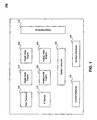
- FIG. 1 is a functional block diagram of a television on a chip, according to an embodiment of the invention.
- FIG. 2 is a detailed functional block diagram of a television on a chip, according to an embodiment of the invention.
- FIG. 1 provides a functional block diagram of television on a chip (TVOC) 100, according to an embodiment of the invention.
- a TVOC includes the functionality necessary to receive and display television signals in a variety of input and output formats.
- a TVOC can be used in set-top boxes for cable and satellite television, or directly within a television. All functionality provided can be provided on a single integrated circuit.
- TVOC 100 includes data transport 105, IF demodulator 110, digital audio engine 115, analog audio engine 120, digital video engine 125, analog video engine 130, output interfaces 135, control interfaces 140, ancillary interfaces 145, and system controller 150.
- Data transport 105 can receive digital video data and performs preprocessing of the data for use throughout other TVOC 100 components.
- IF demodulator 110 contains functionality to receive analog television signals and perform processing to produce digital and analog video and audio signals for use within the other components of TVOC 100.
- Digital audio engine 115 can process digital audio signals, while analog audio engine 120 can process analog audio signals.
- digital video engine 125 can process digital video signals, while analog video engine 130 can process analog video signals.
- Digital video engine 125 and analog video engine 130 also have the capability to process graphics, and integrate those graphics within the video and audio outputs.
- Output interfaces 135 can output various types of analog and digital audio and video signals.
- Control interfaces 140 can provide a means for external control of TVOC 100.
- Ancillary interfaces 145 can provide access to various types of ancillary input and output devices, such as access to establish an Ethernet connection with the TVOC 100.
- System controller 150 can control overall operation of the circuitry within TVOC 100.
- FIG. 2 provides a detailed functional block diagram of TVOC 200, according to an embodiment of the invention.
- TVOC implementations will vary depending on the particular environment in which a TVOC will be used. For example, depending on the country of use, a TVOC may be required to support different types of video or audio standards. Additionally, a TVOC may be required to support standard definition, high definition or both types of television signal broadcasts. Increasingly, cable set top box and television set manufacturers require that chips and chip sets support a wide range of standards and uses.
- TVOC 200 provides an embodiment of a TVOC that provides a set of functionalities that meets this need.
- TVOC 200 is provided to illustrate one embodiment of a TVOC, and is not intended to be limiting. Based on the teachings herein, individuals skilled in the relevant arts will be able to ascertain alternative embodiments to TVOC 200. It is intended that these embodiments are within the scope of the invention.
- TVOC 200 includes input elements, video and graphics processing elements, audio processing elements, control elements, control interfaces, output interfaces and ancillary interfaces. Additionally, TVOC 200 includes elements that further facilitate the integration of television functionality on a single integrated circuit.
- the input elements of TVOC 200 include intermediate frequency (IF) demodulator 202 and data transport module 204.
- IF demodulator 202 operates on an analog television signal to produce a digital baseband composite video broadcasting signal (CVBS) and a digital audio signal, such as a monaural or Broadcast Television System Committee (BTSC) baseband multiplex signal.
- the analog input signals can include, among others, National TV System Committee (NTSC), Phase Alternation Line Rate (PAL), and Sequential Couleur Avec Memoire (SECAM) television signals.
- NTSC National TV System Committee
- PAL Phase Alternation Line Rate
- SECAM Sequential Couleur Avec Memoire
- IF demodulator 202 is optionally a digital IF demodulator that receives and demodulates an analog IF input signal to produce a digital audio signal and a digital video signal.
- analog IF input signal is a television signal or channel that has been down-converted from RF
- IF demodulator 110 includes an A/D converter, a first digital complex mixer, a second digital complex mixer, and various digital filters.
- the A/D converter receives the analog IF input signal and converts it to digital.
- the first digital complex mixer receives the output of the A/D converter and down-converts the output of the A/D converter to baseband.
- a picture carrier is recovered from the output of the first digital complex mixer, and fed back to a direct digital synthesizer to control the tuning accuracy of the first digital complex mixer. More specifically, a feedback loop is configured so that the picture carrier is down-converted to DC so as to control the tuning accuracy of the first digital complex mixer.
- the complex output of the first complex mixer is further processed using Nyquist filtering and other filtering to recover the digital video signal. Such filtering may be accomplished using digital signal processing techniques.
- the digital audio signal is recovered by further processing the output of the first digital complex mixer.
- a digital IF demodulator embodiment of IF demodulator 202 is further taught in copending application, U.S. Patent Application No. 10/448,062, filed May 30, 2003, which is incorporated herein by reference in its entirety.
- a secondary audio program (SAP) signal received must be processed in order to generate a pulse code modulated signal (PCM) output signal.
- PCM pulse code modulated signal
- a SAP signal is band pass filtered, FM demodulated, and processed using a variable de-emphasis algorithm to produce the PCM.
- the optional FM demodulation system described above addresses this problem by approximating the denominator during demodulation of an FM signal.
- the FM demodulation system receives a prior estimated value of 1/x(n) and a present value of x(n).
- the FM demodulation system also adjusts the prior estimated value of 1/x(n) to compensate for an error between the prior estimated value of 1/x(n) and the present value of 1/x(n).
- the FM demodulation system outputs an adjusted prior estimated value of 1/x(n) as the present value of 1/x(n).
- Data transport module 204 receives compressed video data, normally in the form of MPEG or DIRECTTV transport streams. Data transport module 204 parses the streams and performs preprocessing. Data transport module 204 can optionally support personal video recording.
- data transport module 204 can optionally include a video data stream front end processor.
- PID program identification
- data packets within a video data stream that are associated with a particular program are allocated within particular time slots of a data frame.
- a distribution device such as a cable system headend, organizes data packets into frames with packets for a particular program channel located in specific time slots within the frames.
- This approach is referred to herein as a time division multiplexing approach.
- An example of this approach is transport stream multiplexing format (TSMF), which has been recently developed by a consortium of television manufacturers for use in Japan.
- TSMF transport stream multiplexing format
- packets will contain a PID.
- the video data stream front end processor provides an efficient way to demultiplex video signals that use both a PID and are multiplexed using a time division multiplexing approach.
- the video data stream front end processor includes syncronizers, parsers, demultiplexers, and an input buffer. Each demultiplexer within the system includes a header detect module, a slot map module, a frame sync module and a packet accept module. The video data stream front end processor analyzes the PID and slot location for each packet received in a data stream, and based on the PID and slot location a packet is either accepted or rejected.
- the video data stream front end processor is further taught in co-pending application, U.S. Patent Application No. 10/640,684, filed Aug. 14, 2003, which is herein incorporated by reference in its entirety.
- data transport module 204 can optionally include a packet substitution module for substituting packets into a data stream.
- packet substitution module for substituting packets into a data stream.
- program channels are transmitted to customer premise devices, such as a television or cable set top box
- data packets for program channels are typically multiplexed together into a video data stream.
- the customer premise device When the video data stream is received by a customer premise device, the customer premise device typically parses the incoming stream to retain only those packets that pertain to the channel of interest to be viewed or recorded.
- the parsing process can create gaps in the data stream where packets associated with channels other than the channel of interest were located.
- the parsing of the stream potentially leaves time gaps where packets were removed.
- system and management information associated with a data stream is likely to change as a result of adjustment in encryption or organization of packets within a data stream, for example.
- different types of information may need to be inserted into a data stream, and the different types of information may have different timing requirements. Different types of information can include, for example, system information for video control, system information for audio control, overall system management information, or customer specific application information.
- the packet substitution module provides a system for efficiently substituting data packets into a data stream.
- the packet substitution module includes a set of packet buffers that buffer packets to be substituted into the data stream.
- the packet substitution module also includes a multiplexer that obtains packets from the set ofpacket buffers and substitutes packets into the data stream. The operation of the multiplexer is controlled by a packet substitution controller.
- a direct memory access engine provides packets for insertion to the packet buffers based on a link list buffer control that is coupled the direct memory access engine.
- the packet substitution module is further taught in co-pending application, U.S. Patent Application No.: 10/640,684, filed Aug. 14, 2003, which is herein incorporated by reference in its entirety.
- data transport module 204 can optionally include a media processing system for processing multiple program channels containing one or more data packets.
- TVOC 200 may use a system time clock that is independent of the system time clock of a transmitting system. Because these system time clocks are asynchronous, the receiver clock may run at a slightly different rate than the transmitter clock. For example, when the receiver clock runs slower than the transmitter clock, data packets arrive faster than the receiver processes them causing the input buffer to overflow.
- the lack ofprecise timing between the transmitter and receiver creates deleterious effects on video display such as lack of synchronization between video and audio.
- a common technique to minimize the impact of these timing errors is to synchronize the system time clock of the receiver to the system time clock of the transmitting device. This clock "locking" technique reduces timing errors associated with data packets from the transmitter on which the receiver clock is locked.
- the media processing system includes a processor, a set of timestamp insertion modules coupled to the processor.
- the number of timestamp insertion modules would be equal to the number of program channels being processed.
- Each timestamp insertion module would include a local program reference clock, a synchronizer that synchronized the local program reference clock to a clock of a device transmitting the program being processed, a local program timestamp generator and an input buffer coupled to the timestamp insertion modules.
- the video processing elements of the TVOC 200 include analog video decoder 210, digital video decoder 212, video and graphics processing module 214, 3D engine 215, 2D engine 216 and video encoder 218.
- Analog video decoder 210 supports high quality decoding of a standard definition composite video broadcasting signal (CVBS) and S-Video signal.
- Digital video decoder 212 decodes video signals that comply with the International Telecommunications Union (ITU) standard ITU-R-656 at varying resolutions including 525i, 625i and 240p.
- ITU International Telecommunications Union
- analog video decoder 210 and/or digital video decoder 212 can optionally include a 2-D adaptive comb filter.
- a composite video signal is the sum of a luminance (brightness) signal and a chrominance (color) signal. These signals are also referred to as luma and chroma signals, respectively.
- the frequency ranges of the luma and chroma signals are designed to overlap. A problem created by overlapping the luma and chroma frequency spectra is that it is difficult to separate them completely.
- 2-D adaptive comb filter addresses this challenge.
- 2-D adaptive comb filter filters the video information both horizontally along the scan lines and vertically between the horizontal scan lines.
- a low-pass or bandpass filter is used.
- a combing procedure is used.
- Adaptive logic solves the problem of combing at a vertical color transition point. The logic examines three successive horizontal scan lines simultaneously. At a vertical transition between two colors, either the top two or bottom two scan lines will usually be the same. Initially, for example, the top two of three scan lines will be the same color. The logic directs those lines to a digital version of the comb filter. When the scan moves down another line, the scan line triplet includes a new bottom line. The bottom two scan lines of the new triplet will have the new color, and the bottom lines will be directed to the comb filter. In this manner, two lines with different colors are not input to the comb filter at a transition boundary.
- the 2D adaptive comb filter includes a band limiting filter, a decision stage, a blending stage, and a processor.
- a composite video signal including luma and chroma subcarriers enters the band limiting filter after passing through an analog-to-digital converter. After band limiting filter, the original signal is split among three different paths.
- the first path is a decision stage.
- the decision stage includes a wide bandpass filter, interpolator, and chroma decision logic.
- the second path is the blending stage.
- the blending stage includes a narrow bandpass filter, a chroma comb filter, and a blending module.
- the third path leads directly to the processor.
- the 2D adaptive comb filter is further taught in co-pending application, U.S. Patent Application No. 10/641,160, filed Aug. 15, 2003, which is herein incorporated by reference in its entirety.
- digital video decoder 212 can optionally include an artificial time stamp module that generates pseudo MPEG information from received digital video information, such as DV25 and DV50 information generated by digital video cameras. This DV25 and DV50 information lacks timestamps used by MPEG signal processors. An artificial time stamp module generates timestamps that are inserted into the DV25 or DV50 information, thereby facilitating decoding by an MPEG signal processor. An artificial time stamp module is further taught in co-pending application, U.S. Patent Application No. 10/640,648, filed Aug. 14, 2003, which is herein incorporated by reference in its entirety.
- digital video decoder 212 can optionally include a teletext decoder system for processing teletext message sequences.
- the teletext decoder provides a system for efficiently decoding and detecting valid teletext message sequences.
- the teletext decoder system includes a correlator, a sine wave generator, two time window generators, a phase detector, a framing code search engine, and a match filter.
- the teletext decoder system determines the phase of the run-in burst of a teletext message sequence, identifies the framing code location, decides whether the teletext sequence is valid and decodes the teletext data for display.
- the teletext decoder system is further taught in copending applications, U.S.
- Video and graphics processing module 214 includes a variety of functions for processing video and graphics, and for integrating video and graphics.
- video and graphics processing module 214 can optionally include MPEG, graphics and video feeders; video scalers; capture blocks; and/or video compositors for combining video and graphics.
- 3D engine 215 provides low bandwidth three dimensional (3D) graphics rendering for set-top boxes and television displays without sacrificing the performance needed for Internet e-commerce 3D applications and games.
- video and graphics processing module 214 can optionally include a combined color look-up and gamma correction system.
- Color look-up table and gamma correction routines are used to improve video graphics displayed on a television.
- the combined color look-up and gamma correction system includes a memory having color look up table (CLUT) parameters and gamma correction parameters stored therein.
- CLUT color look up table
- the combined color look-up and gamma correction system includes an input matrix configured to receive first and second type pixel data. Memory is coupled to the input matrix and configured to associate one of the first and second type pixel data with the stored CLUT parameters and associate the other of the first and second type pixel data with the stored gamma correction parameters.
- the pixel contains all the color component information (e.g., YUV422 or ARGB8888).
- the pixel contains an index (e.g., CLUT format).
- CLUT format In order to support CLUT format and Gamma-correction function, conventionally two separate RAMs were needed. In the combined color look-up and gamma correction system, however, the CLUT function is combined with the gamma-correction function by applying a gamma-correction equation on the color look-up-table.
- the combined color look-up and gamma correction system provides one RAM for sharing both CLUT and gamma correction functions. More specifically, one RAM arrangement is integrated such that the same RAM can be used for CLUT + Gamma-Correction (for CLUT format) or just Gamma-Correction (for other formats). This RAM arrangement provides economies in terms of space savings on the integrated TVOC 200 circuit, by providing for a more efficient process to implement CLUT and gamma correction functions. Additionally, the combined color look-up and gamma correction system provides a more efficient software setup that does not require special arrangements or address swapping. Combined color look-up and gamma correction system is further taught in co-pending application, U.S. Patent Application No. 10/640,666, filed Aug. 14, 2003, which is incorporated herein by reference in its entirety.
- Video encoder 218 encodes processed video signals for output to a display.
- Video encoder 218 can optionally support both standard and high definition video signals.
- Video encoder 218 supports a variety of analog video standards (e.g., NTSC, PAL, SECAM, 480i, 480p, 720p, and 1080i), as well as digital video standards (e.g., ITU-R-656 and support for digital video interface (DVI) encoding). Additionally, video encoder 218 can receive video blanking interval (VBI) signals.
- VBI video blanking interval
- Video encoder 218 combines these VBI signals with appropriate lines of video to support arrangements, such as closed captioning and teletext.
- video encoder 218 can optionally include a timing generator that generates time-dependent control signals for video signals.
- control signals support outputting video signals in different formats and to implement a variety of value added features including, for example, copy protection features, such as those contained within MACROVISION copy protection process standards.
- MACROVISION is a trademark of Macrovision Corporation.
- the timing generator includes a set of microsequencers, a programmable combinational logic (PCL) module, shared memory, an arbiter for sharing of memory by the microsequencers, stacks containing registers for microsequencer control, and a control interface.
- the timing generator can provide control signals for video signals, implement the MACROVISION copy protection process, and provide other value added features.
- Flags generated by the microsequencers are processed to generate one or more control signals used to support the outputting of video signals including those requiring MACROVISION copy protection.
- the generation of control signals is software controlled, thereby allowing the system to be reconfigured in real time, and permitting modifications to reflect changes in the MACROVISION copy protection process and other value added features for video signals.
- the invention provides an efficient way to flexibly produce time-dependent control signals for video signals.
- the timing generator is further taught in co-pending application, U.S. Patent Application No. 10/640,627, filed Aug. 14, 2003, which is hereby incorporated in its entirety.
- video encoder 218 can optionally include an MPAA (Motion Picture Association of America) HDTV (High Definition Television) copy protection filter system.
- MPAA Motion Picture Association of America
- HDTV High Definition Television
- the MPAA HDTV copy protection filter system provides an efficient system to reduce the resolution of a digital video signal to comply with the MPAA copy protection standards by integrating copy protection filters with elements of video encoder 218.
- the copy-protection filter is a low-pass horizontal filter.
- the copy-protection filter is a low-pass vertical filter.
- a combination horizontal and vertical filter are used. For each filter, any number of taps may be used.
- the copy-protection filter may be placed in an analog data path in the video encoder before the signal is converted to an analog signal.
- a digital data path is coupled to the analog data path.
- the copy-protection filter can be placed on the analog data path after the connection between the analog and digital data paths.
- a second copy-protection filter can be placed in the digital data path.
- the second copy-protection filter may be operated independently of the first copy-protection filter.
- the copy-protection filter may be combined with other filters in the system.
- the copy-protection filter may be combined with a video scaler before the initial video data stream enters the compositor.
- the audio processing elements of TVOC 200 include audio decoder 220 and audio processor 222.
- Audio decoder 220 can receive a baseband analog BTSC composite signal that was extracted by IF demodulator 202 and process the received signal to recover the main, stereo and SAP channels contained within the original signal.
- Audio decoder 220 can support BTSC and CPZ503 (used in Japan) standards for composite signals.
- an optional digital interface is coupled between IF demodulator 202 and a digital signal processor (DSP) within audio decoder 220.
- DSP digital signal processor
- a potentiometer or implementation of an automatic gain control (AGC) algorithm in a digital signal processor within audio decoder 202 can be used to adjust the signal levels of right and left stereo signals.
- AGC automatic gain control
- IF demodulator 202 has an output that is scalable to ensure compatibility with different down-stream DSP devices.
- the output of the IF demodulator 202 is a digital signal, including composite BTSC samples that are compatible with multi-channel television sound (MTS) standards. Because the output includes digital composite samples, the digital interface can provide signals to the DSP in the digital domain.
- MTS multi-channel television sound
- audio decoder 220 can optionally include a signal mode detection system.
- the signal mode detection system can be used, for example, to distinguish mono, dual mono and stereo modes in an audio transmission.
- the signal mode detection system can include a first bandpass filter, a first envelope tracker coupled to the first bandpass filter, a second bandpass filter, a second envelope tracker coupled to the second bandpass filter, and a decision circuit coupled to both the first and second envelope trackers.
- the decision circuit is configured to process decision logic to determine whether an audio transmission is in mono, dual mono, or stereo mode.
- the signal mode detection system is particularly useful for processing Japanese Broadcast Television Systems Committee (JBTSC) standard audio broadcast signals, which have three modes of transmission.
- JBTSC Japanese Broadcast Television Systems Committee
- audio decoder 220 can optionally include a JBTSC signal separation processor.
- the main channel includes the audio signal.
- the sub channel includes the difference between a right and left channel stereo signal contained in the main channel.
- the control signal includes information indicating the mode of transmission.
- the JBTSC signal separation processor supports the processing of all three channels.
- the JBTSC signal separation processor includes a sub path, a main path and a separator.
- the sub path includes a bandpass filter, a first filter path, a second filter path, an FM demodulator, a lowpass filter and a de-emphasis circuit.
- the JBTSC signal separation processor provides optimal separation of left and right stereo signals within a JBTSC.
- the JBTSC signal separation processor is further taught in co-pending application, U.S. Patent Application No. 10/641,161, filed Aug. 15, 2003, which is incorporated herein by reference in its entirety.
- audio decoder 220 can optionally include a digital signal processor (DSP) decoder having an execution unit, an address generator and an instruction set that can be used to decode input signals.
- DSP digital signal processor
- the programmable address generator enables the execution unit to perform register addressing, indirect addressing and immediate addressing.
- An advantage of a DSP is that is reprogrammable and updateable.
- a DSP decoder can also be used within digital video decoder 212 and analog video decoder 210.
- the DSP decoder is further taught in co-pending application, U.S. Patent Application No.: 10/641,295, filed Aug. 15, 2003, which is incorporated herein by reference in its entirety.
- a sampled signal can be converted to a higher data rate signal.
- sampled signals often need to be converted to higher or lower sample rates.
- Conventional sample rate converters suffer from a variety of drawbacks.
- conventional SRCs typically interpolate between existing sample points to obtain new sample points. The interpolation is typically performed using known, pre-determined, fixed ratios between the lower data rate and the higher data rate. Results are then clocked out at the higher data rate. Such an interpolation is not performed in real time.
- the higher data rate clock is affected by jitter or small/large frequency variations, for example, the higher data rate output does not necessarily track the lower data rate data.
- the method to convert a sampled signal to a higher data rate involves receiving conversion pulses having a conversion rate that is higher than a sample rate of the sampled signal. Next, two sample points on either side of a conversion pulse are reconstructed in real time from the sample signal. An amplitude between the two reconstructed sample points is then interpolated. The output of the interpolated amplitude is output in real time. This process is repeated on subsequent conversion pulses, such that the outputted interpolated amplitudes form the higher data rate signal having a data rate equal to the conversion rate.
- This sample rate conversion method is further taught in co-pending application, U.S. Patent Application No.: 10/641,034, filed Aug. 15, 2003, which is incorporated herein by reference in its entirety.
- Audio processor 222 analyzes and processes audio signals in a variety of formats including Dolby digital and MPEG audio. Audio processor 222 delivers processed audio signals to audio outputs, including digital audio port 258 and analog audio port 259.
- the control interfaces can include DDR ⁇ DRAM controller 240, EJTAG module 242, peripheral interfaces 244, and EBI interface 246.
- DDR-DRAM controller 240 supports the use of external DDR-DRAM.
- EJTAG module 242 supports advanced debugging features, including software debug of user and kernel code.
- Peripheral interfaces 244 provide a range of interfaces to support smart card usage, and the like.
- EBI (external bus interface) interface 246 supports the connection of external SRAMs, flash memories, EPROMs, and interfaces with additional external peripherals.
- the output interfaces can include S-Video composite interface 250, DVI interface 252, 656 Interface 254, RF Mod interface 256, digital audio port 258 and analog audio port 259.
- the S-Video composite interface 250 can output video signals in a variety of formats including SCART1, S-Video, and composite video (CVBS) outputs.
- DVI interface 252 provides an output interface for DVI signals.
- 656 Interface 254 provides an output interface for analog video signals that comply with the ITU-R-656 standard.
- RF Mod interface 256 provides an output interface for an analog composite television signal which is suitable for demodulation by a television demodulator.
- Digital audio port 258 and analog audio port 259 provide interfaces for digital and analog audio signals, respectively.
- the ancillary interfaces can include V.90 interface 260, USB 2.0 interface 262, Ethernet interface 264, and SATA interface 266.
- V.90 interface 260 provides an interface to modems using the V.90 standard.
- USB 2.0 interface 262 provides an interface to devices using a USB 2.0 standard.
- Ethernet interface 264 provides an interface to connect TVOC 200 to an Ethernet or provide Internet connectivity.
- SATA interface 266 provides an interface for use with external hard drives.
- System controller 270 provides overall control for TVOC 200.
- Additional optional elements within TVOC 200 that further facilitate the integration of television functionality on a single integrated circuit can include a reset synchronization system.
- the reset synchronization system synchronizes a reset signal with a local clock within TVOC 200. Proper synchronization of a reset signal with a local clock is important to ensure seamless operation of TVOC 200 during a reset.
- the reset synchronization system includes a local clock terminal, a reset terminal, a synchronized reset output terminal, and synchronizing circuitry coupled between the clock terminal, the reset terminal, and the synchronized reset output terminal.
- the synchronizing circuitry synchronizes a received reset signal to the local clock signal and outputs a synchronized reset signal on the synchronized reset output terminal.
- a reset synchronization system is further taught is co-pending application, U.S. Patent Application No.: 10/640,632, filed Aug. 14, 2003, which is incorporated herein by reference in its entirety.
- Optional elements within TVOC 200 that further facilitate the integration of television functionality on a single integrated circuit further include an I/O (input/output) multiplexing system.
- Integrated circuits, such as TVOC 200 communicate with other chips through I/O devices (e.g., pins or pads).
- I/O devices e.g., pins or pads.
- function blocks are becoming smaller, and the chips denser, there is limited area on the chip for the I/O devices.
- groups or sets of the function blocks share the I/O devices.
- a controlling system e.g., a multiplexer
- the I/O multiplexing system addresses the need to conserve space on TVOC 200 while also ensuring proper timing.
- the I/O multiplexing system includes an input/output device including a bidirectional pad, function blocks coupled to the I/O device and an I/O multiplexing module that controls transmission of the signals between the function blocks and the I/O device using a controller.
- the I/O multiplexing module can include a data I/O multiplexer and an enable I/O multiplexer coupled to the controller.
- the I/O multiplexing module can include a data re-clocking device coupled to the I/O device, the function blocks, and the data I/O multiplexer.
- the re-clocking device synchronizes one or more of the signals with a system clock before the one or more signals enter the data I/O multiplexer.
- the I/O multiplexing module also includes an enable re-clocking device coupled to the I/O device, the function blocks, and the enable I/O multiplexer.
- the re-clocking device synchronizes one or more of the signals with a system clock before the one or more signals enter the enable I/O multiplexer.
- Optional elements within TVOC 200 that further facilitate the integration of television functionality on a single integrated circuit can further include an adaptable strapping system.
- TVOC 200 can have numerous selectable functions, for example, selectable video encoding standards.
- a mode or state can be selected for TVOC 200 based on the product it is incorporated within.
- the mode or state can be selected using a strapping system (e.g., mode or state setting system) in a variety of ways, including using a dedicated pin, a register control block controlled by software running in the product, or the like.
- a function of the device can be set using a signal that designates a mode or state.
- the adaptable strapping system of the present invention allows TVOC 200 to use alternate functions after packaging in real time.
- the adaptable strapping system includes a control system that controls a mode of TVOC 200, an initialization system that transmits a signal to the control system to initialize TVOC 200, an internal strapping system that transmits a signal to the control system that can be sued to place TVOC 200 in a first state, and an override system that transmits a second signal to the control system to place TVOC 200 in a second state.
- the adaptable strapping system is further taught in co-pending application, U.S. Patent Application No. 10/641,103, filed Aug. 15, 2003, which is incorporated by reference herein in its entirety.
- Optional elements within TVOC 200 that further facilitate the integration of television functionality on a single integrated circuit can further include a system for multi-channel audio interconnects.
- Traditional processing of audio signals transferred between audio modules, such as analog-to-digital converters, error correction devices and digital filters, within a printed circuit board or an IC typically requires conversion of the related audio signals to an inter-IC sound (I 2 S) standard or a similar format.
- I 2 S is one technique intended to standardize the format of audio data transferred between these internal components.
- Components implementing the widely accepted I 2 S standard convert incoming audio data signals into the I 2 S format.
- the system for multi-channel audio interconnects provides a data bus that can be used to transfer audio data that minimizes the complexities and amount of hardware required for transferring audio data between modules.
- a suite of protocols support this bus to more efficiently transfer data between the modules, ultimately reducing the number of chip pins.
- a multi-channel audio interconnect system includes data paths that are configured for transferring audio data between a transmitting module and one or more receiving modules.
- the multi-channel audio interconnect system includes an encoder positioned within the transmitting module and configured to convert audio data requiring transmission into two-line audio information segments.
- the audio information segments include a format portion identifying the audio format and a data portion for carrying the audio data.
- a data line and a synchronization line exist between audio modules.
- the data line carries the audio information segments, while the synchronization line transmits a number of sync pulses that indicate a start of one of the audio information segments.
- a decoder is included in a receiving module that interprets the audio information segments and sync pulses.
- Optional elements within TVOC 200 that further facilitate the integration of television functionality on a single integrated circuit can include circuits and methods to enhance scan testing.
- Scan testing provides an effective means to test the structural integrity of devices, such as flip-flops, within a complex integrated circuit, such as TVOC 200.
- features may be enabled or disabled depending upon TV manufacturer preferences. This flexibility can make scan testing more complex. Circuits to support scan testing and reduce this complexity can be provided.
Abstract
Description
Claims (10)
- An integrated circuit for providing television functionality, comprising:a data transport module for receiving digital video and audio data and performing preprocessing of the data;an IF demodulation module for receiving and preprocessing analog television signals;a digital audio engine for processing digital audio signals;an analog audio engine for processing analog audio signals;a digital video engine for processing digital video signals; and aanalog video engine for processing analog video signals, wherein said data transport module, said IF demoduation module, said digital audio engine, said analog audio engine, said digital video engine and said analog video engine are coupled through a system controller.
- An integrated circuit for providing television functionality, comprising:a plurality of input elements;video and graphics processing elements;audio processing elements;output interfaces; anda control element, wherein said plurality of input elements, said video and graphics processing elements, said audio processing elements, and said output interfaces are coupled through a system controller.
- The integrated circuit of claim 2, wherein said plurality of input elements comprise:an IF demodulator; anda data transport module.
- The integrated circuit of claim 3, wherein said IF demodulator comprises a digital IF demodulator.
- The integrated circuit of claim 3, wherein said IF demodulator includes an FM demodulation system for approximating y(n)=1/x(n) in FM demodulation, where x(n)=I2(n)+Q2(n).
- The integrated circuit of claim 3, wherein said data transport module includes a video data stream front end processor.
- The integrated circuit of claim 3, wherein said data transport module includes a packet substitution module.
- The integrated circuit of claim 3, wherein said data transport module includes a media processing system.
- The integrated circuit of claim 2, wherein said video and graphics processing elements comprise:an analog video decoder;a digital video decoder;a video and graphics processing module coupled to said analog video decoder and said digital video decoder; anda video encoder coupled to said video and graphics processing module.
- An integrated circuit, comprising:a digital IF demodulator for receiving and demodulating analog television signals;an FM modulation system for approximating y(n)=1/x(n) in FM demodulation, where x(n)=I2(n)+Q2(n);a video data stream front end processor for demultiplexing video signals that us both a program identifier and are multiplexed using a time division multiplexing approach;a packet substitution module for substituting packets into a video data stream;a media processing system for processing multiple program channels containing one or more data packets;a 2D adaptive comb filter for separating luma and chroma signals within a compositie video signal;an artificial time stamp module that generates pseudo MPEG information from received DV25 or DV50 digital video information;a 2D engine that provides two dimensional graphics processing;a 3D engine that provides three dimensional graphics processing;a combined color look-up and gamma correction system that improves video graphics;a timing generator for generating time-dependent control signals for video signals;a teletext decoder system for processing teletext sequences;a MPAA HDTV copy protection filter system for providing MPAA HDTV copy protection;an audio decoder digital interface coupled between a IF demodulator and an audio decoder the provides and all digital interface and reduces signal mismatch;signal mode detection system that determine a transmission mode of a broadcast signal; anda digital signal processor within an audio decoder, wherein said digital signal processor is reprogrammable and updateable.
Applications Claiming Priority (54)
| Application Number | Priority Date | Filing Date | Title |
|---|---|---|---|
| US640648 | 1984-08-14 | ||
| US640632 | 1984-08-14 | ||
| US641160 | 1984-08-16 | ||
| US629781 | 1990-12-17 | ||
| US641031 | 1991-01-14 | ||
| US641103 | 1996-04-29 | ||
| US629797 | 2000-07-31 | ||
| US641034 | 2000-08-16 | ||
| US640686 | 2000-08-18 | ||
| US45126503P | 2003-03-04 | 2003-03-04 | |
| US451265P | 2003-03-04 | ||
| US46757403P | 2003-05-05 | 2003-05-05 | |
| US467574P | 2003-05-05 | ||
| US10/448,062 US7239357B2 (en) | 2000-12-15 | 2003-05-30 | Digital IF demodulator with carrier recovery |
| US448062 | 2003-05-30 | ||
| US10/629,781 US7102689B2 (en) | 2003-05-05 | 2003-07-30 | Systems and methods for decoding teletext messages |
| US10/629,797 US20050027771A1 (en) | 2003-07-30 | 2003-07-30 | System and method for approximating division |
| US10/640,682 US7450617B2 (en) | 2003-08-14 | 2003-08-14 | System and method for demultiplexing video signals |
| US10/640,686 US7089471B2 (en) | 2003-08-14 | 2003-08-14 | Scan testing mode control of gated clock signals for flip-flops |
| US640649 | 2003-08-14 | ||
| US10/640,649 US7532648B2 (en) | 2003-08-14 | 2003-08-14 | System and method using an I/O multiplexer module |
| US640687 | 2003-08-14 | ||
| US640684 | 2003-08-14 | ||
| US640682 | 2003-08-14 | ||
| US10/640,666 US7535476B2 (en) | 2003-08-14 | 2003-08-14 | Method and system color look-up table (CLUT) random access memory arrangement for CLUT and gamma correction application |
| US10/640,632 US7260166B2 (en) | 2003-08-14 | 2003-08-14 | Systems for synchronizing resets in multi-clock frequency applications |
| US10/640,627 US7555125B2 (en) | 2003-08-14 | 2003-08-14 | Systems and methods for generation of time-dependent control signals for video signals |
| US10/640,684 US7561597B2 (en) | 2003-08-14 | 2003-08-14 | System and method for data packet substitution |
| US10/640,659 US7058868B2 (en) | 2003-08-14 | 2003-08-14 | Scan testing mode control of gated clock signals for memory devices |
| US10/640,648 US7715482B2 (en) | 2003-08-14 | 2003-08-14 | System and method for generating pseudo MPEG information from digital video information |
| US640627 | 2003-08-14 | ||
| US640659 | 2003-08-14 | ||
| US10/640,687 US7131045B2 (en) | 2003-08-14 | 2003-08-14 | Systems and methods for scan test access using bond pad test access circuits |
| US640666 | 2003-08-14 | ||
| US49512703P | 2003-08-15 | 2003-08-15 | |
| US49512903P | 2003-08-15 | 2003-08-15 | |
| US49512103P | 2003-08-15 | 2003-08-15 | |
| US10/641,161 US20050036626A1 (en) | 2003-08-15 | 2003-08-15 | Method and system for processing a Japanese BTSC signal |
| US641295 | 2003-08-15 | ||
| US10/641,103 US7263627B2 (en) | 2003-08-15 | 2003-08-15 | System and method having strapping with override functions |
| US10/641,034 US7409339B2 (en) | 2003-08-15 | 2003-08-15 | Methods and systems for sample rate conversion |
| US10/641,295 US20050036357A1 (en) | 2003-08-15 | 2003-08-15 | Digital signal processor having a programmable address generator, and applications thereof |
| US10/641,160 US7688387B2 (en) | 2003-08-15 | 2003-08-15 | 2-D combing in a video decoder |
| US10/641,031 US7679629B2 (en) | 2003-08-15 | 2003-08-15 | Methods and systems for constraining a video signal |
| US10/641,004 US7457420B2 (en) | 2003-08-15 | 2003-08-15 | Method and system for detecting signal modes in a broadcast audio transmission |
| US641004 | 2003-08-15 | ||
| US495121P | 2003-08-15 | ||
| US641161 | 2003-08-15 | ||
| US495127P | 2003-08-15 | ||
| US495129P | 2003-08-15 | ||
| US646721 | 2003-08-25 | ||
| US10/646,833 US7764671B2 (en) | 2003-08-15 | 2003-08-25 | Method and system for a multi-channel audio interconnect bus |
| US646833 | 2003-08-25 | ||
| US10/646,721 US20050036074A1 (en) | 2003-08-15 | 2003-08-25 | Method and system for a digital interface for TV stereo audio decoding |
Publications (2)
| Publication Number | Publication Date |
|---|---|
| EP1501284A2 true EP1501284A2 (en) | 2005-01-26 |
| EP1501284A3 EP1501284A3 (en) | 2012-02-15 |
Family
ID=33494451
Family Applications (1)
| Application Number | Title | Priority Date | Filing Date |
|---|---|---|---|
| EP04005181A Withdrawn EP1501284A3 (en) | 2003-03-04 | 2004-03-04 | Apparatus, system and methods for providing television functionality on a chip |
Country Status (2)
| Country | Link |
|---|---|
| US (3) | US7489362B2 (en) |
| EP (1) | EP1501284A3 (en) |
Cited By (6)
| Publication number | Priority date | Publication date | Assignee | Title |
|---|---|---|---|---|
| US7610013B2 (en) | 2005-04-18 | 2009-10-27 | Marvell World Trade Ltd. | Wireless audio for entertainment systems |
| CN102685416A (en) * | 2011-01-06 | 2012-09-19 | 硅实验室股份有限公司 | Receiver and method of receiving analog and digital television signals |
| CN103618892A (en) * | 2013-12-02 | 2014-03-05 | 广州创维平面显示科技有限公司 | Method for detecting television and television |
| CN105933073A (en) * | 2016-06-28 | 2016-09-07 | 成都育芽科技有限公司 | Ultrasonic coding and decoding system based on wireless acoustic signals and computing method |
| CN109581861A (en) * | 2017-09-29 | 2019-04-05 | 上海微电子装备(集团)股份有限公司 | Move bench control system, sports platform system and exposure device |
| CN110445993A (en) * | 2019-08-23 | 2019-11-12 | 中国航空无线电电子研究所 | A kind of video acquisition system of no phase-locked loop clock |
Families Citing this family (20)
| Publication number | Priority date | Publication date | Assignee | Title |
|---|---|---|---|---|
| US7847864B1 (en) * | 2002-03-01 | 2010-12-07 | Broadcom Corporation | All digital radio frequency modulator |
| US7489362B2 (en) * | 2003-03-04 | 2009-02-10 | Broadcom Corporation | Television functionality on a chip |
| KR100662902B1 (en) * | 2004-03-09 | 2007-01-02 | 삼성전자주식회사 | Optical reproducing apparatus capable of generating DVI digital signal and reproducing method thereof |
| US7639308B2 (en) | 2004-04-19 | 2009-12-29 | Broadcom Corporation | Television channel selection canvas |
| US20050235329A1 (en) * | 2004-04-19 | 2005-10-20 | Broadcom Corporation | Systems and methods for integrated control within a home entertainment system |
| US8065707B1 (en) * | 2005-01-03 | 2011-11-22 | Matrox Electronic Systems Ltd. | HDTV set-top box/PC client/server secure video system |
| US20070113260A1 (en) * | 2005-11-16 | 2007-05-17 | Phison Electronics Corp. | [storage media with receiving digital television signal function] |
| US20070169153A1 (en) * | 2006-01-18 | 2007-07-19 | Realfine (Shenzhen) Electronics Co., Ltd. | Embeded USB interface circuit in AV device for recording programs |
| WO2010098134A1 (en) * | 2009-02-27 | 2010-09-02 | パナソニック株式会社 | Recording medium, reproduction device, and integrated circuit |
| WO2010100875A1 (en) * | 2009-03-02 | 2010-09-10 | パナソニック株式会社 | Recording medium, reproduction device, and integrated circuit |
| JP5508819B2 (en) * | 2009-11-13 | 2014-06-04 | オリンパス株式会社 | Receiver |
| JP2011176801A (en) * | 2010-01-26 | 2011-09-08 | Panasonic Corp | Electronic device |
| TWI406561B (en) * | 2010-07-27 | 2013-08-21 | 私立中原大學 | Video processor and its automatic selection filter of the video filter driver |
| JP2012039476A (en) * | 2010-08-09 | 2012-02-23 | Sony Corp | Transmitter-receiver and transmission/reception method |
| US8718806B2 (en) * | 2011-09-02 | 2014-05-06 | Apple Inc. | Slave mode transmit with zero delay for audio interface |
| JP6683598B2 (en) * | 2013-03-15 | 2020-04-22 | マックスサイト インコーポレーティッド | Methods and compositions for producing stable transfected cells |
| CN105120184B (en) * | 2015-10-09 | 2018-06-19 | 深圳市捷视飞通科技有限公司 | A kind of HD video based on FPGA is seamless matrix system |
| FR3095310B1 (en) * | 2019-04-16 | 2021-04-30 | Transdev Group | Electronic device for transmitting a video stream, vehicle, electronic monitoring system and associated method |
| TWI743800B (en) * | 2020-05-22 | 2021-10-21 | 瑞昱半導體股份有限公司 | Circuitry and method for detecting audio standard of sound intermediate frequency signal |
| CN113747144A (en) * | 2020-05-28 | 2021-12-03 | 瑞昱半导体股份有限公司 | Circuit and method for detecting system of sound intermediate frequency signal |
Citations (2)
| Publication number | Priority date | Publication date | Assignee | Title |
|---|---|---|---|---|
| US20030086695A1 (en) * | 2001-11-08 | 2003-05-08 | Hitachi, Ltd. | Video information outputting apparatus, video information receiving apparatus, video information outputting method and video information transmitting method |
| US6570990B1 (en) * | 1998-11-13 | 2003-05-27 | Lsi Logic Corporation | Method of protecting high definition video signal |
Family Cites Families (258)
| Publication number | Priority date | Publication date | Assignee | Title |
|---|---|---|---|---|
| JPS5596773A (en) | 1979-01-19 | 1980-07-23 | Hitachi Ltd | Discrimination unit |
| US4300207A (en) | 1979-09-25 | 1981-11-10 | Grumman Aerospace Corporation | Multiple matrix switching system |
| US4521858A (en) | 1980-05-20 | 1985-06-04 | Technology Marketing, Inc. | Flexible addressing and sequencing system for operand memory and control store using dedicated micro-address registers loaded solely from alu |
| US4419746A (en) | 1980-10-14 | 1983-12-06 | Texas Instruments Incorporated | Multiple pointer memory system |
| US4534054A (en) | 1980-11-28 | 1985-08-06 | Maisel Douglas A | Signaling system for FM transmission systems |
| US4532587A (en) | 1981-08-26 | 1985-07-30 | Texas Instruments Incorporated | Single chip processor connected to an external memory chip |
| DE3274936D1 (en) * | 1981-09-26 | 1987-02-05 | Bosch Gmbh Robert | Digital demodulator for frequency-modulated signals |
| US4399329A (en) | 1981-11-25 | 1983-08-16 | Rca Corporation | Stereophonic bilingual signal processor |
| JPS58121473U (en) | 1982-02-09 | 1983-08-18 | ソニー株式会社 | audio multiplex receiver |
| US4502078A (en) | 1982-02-22 | 1985-02-26 | Rca Corporation | Digital television receivers |
| US4493077A (en) | 1982-09-09 | 1985-01-08 | At&T Laboratories | Scan testable integrated circuit |
| US4623926A (en) | 1982-11-12 | 1986-11-18 | Matsushita Electric Industrial Co., Ltd. | Television synchronous receiver |
| US4577157A (en) | 1983-12-12 | 1986-03-18 | International Telephone And Telegraph Corporation | Zero IF receiver AM/FM/PM demodulator using sampling techniques |
| US4716589A (en) | 1984-11-26 | 1987-12-29 | Nec Corporation | Multivoice signal switching circuit |
| US4628539A (en) | 1985-02-25 | 1986-12-09 | Rca Corporation | Muting circuit |
| US4893316A (en) | 1985-04-04 | 1990-01-09 | Motorola, Inc. | Digital radio frequency receiver |
| GB2176356A (en) * | 1985-06-12 | 1986-12-17 | Philips Electronic Associated | Method of, and demodulator for, digitally demodulating an ssb signal |
| JPS6220488A (en) | 1985-07-19 | 1987-01-29 | Toshiba Corp | Teletext broadcasting receiver |
| US4656651A (en) | 1985-09-09 | 1987-04-07 | Itt Corporation | System for providing remote services |
| US5522082A (en) | 1986-01-23 | 1996-05-28 | Texas Instruments Incorporated | Graphics display processor, a graphics display system and a method of processing graphics data with control signals connected to a central processing unit and graphics circuits |
| US5134691A (en) | 1986-04-01 | 1992-07-28 | Westinghouse Electric Corp. | Bidirectional communication and control network with programmable microcontroller interfacing digital ICs transmitting in serial format to controlled product |
| US4747140A (en) | 1986-12-24 | 1988-05-24 | Rca Corporation | Low distortion filters for separating frequency or phase modulated signals from composite signals |
| US5283903A (en) | 1986-12-25 | 1994-02-01 | Nec Corporation | Priority selector |
| US6539497B2 (en) | 1987-06-02 | 2003-03-25 | Texas Instruments Incorporated | IC with selectively applied functional and test clocks |
| US6760866B2 (en) * | 1987-06-02 | 2004-07-06 | Texas Instruments Incorporated | Process of operating a processor with domains and clocks |
| JPS6448504A (en) | 1987-08-18 | 1989-02-23 | Mitsubishi Electric Corp | Fm demodulator |
| US5287511A (en) | 1988-07-11 | 1994-02-15 | Star Semiconductor Corporation | Architectures and methods for dividing processing tasks into tasks for a programmable real time signal processor and tasks for a decision making microprocessor interfacing therewith |
| US4918531A (en) * | 1988-10-25 | 1990-04-17 | Thomson Consumer Electronics, Inc. | Commercial message timer |
| US4996597A (en) * | 1989-04-20 | 1991-02-26 | Rca Licensing Corporation | User programmable switching arrangement |
| US5031233A (en) | 1989-07-11 | 1991-07-09 | At&E Corporation | Single chip radio receiver with one off-chip filter |
| US5227863A (en) | 1989-11-14 | 1993-07-13 | Intelligent Resources Integrated Systems, Inc. | Programmable digital video processing system |
| US5396635A (en) * | 1990-06-01 | 1995-03-07 | Vadem Corporation | Power conservation apparatus having multiple power reduction levels dependent upon the activity of the computer system |
| KR970000147B1 (en) | 1991-01-31 | 1997-01-04 | 삼성전자 주식회사 | Multi-channel sound recording and reproducing system |
| US5235600A (en) | 1991-03-21 | 1993-08-10 | Amdahl Corporation | Scannable system with addressable clock suppress elements |
| KR100272622B1 (en) | 1991-05-08 | 2000-11-15 | 가나이 쓰도무 | Data processing device |
| US5151926A (en) | 1991-05-21 | 1992-09-29 | General Electric Company | Sample timing and carrier frequency estimation circuit for sine-cosine detectors |
| US5271023A (en) | 1991-06-03 | 1993-12-14 | Motorola, Inc. | Uninterruptable fault tolerant data processor |
| JP3063334B2 (en) | 1991-12-19 | 2000-07-12 | 日本電気株式会社 | Highly reliable information processing equipment |
| US5294982A (en) | 1991-12-24 | 1994-03-15 | National Captioning Institute, Inc. | Method and apparatus for providing dual language captioning of a television program |
| US5475628A (en) | 1992-09-30 | 1995-12-12 | Analog Devices, Inc. | Asynchronous digital sample rate converter |
| US5428404A (en) | 1993-01-29 | 1995-06-27 | Scientific-Atlanta, Inc. | Apparatus for method for selectively demodulating and remodulating alternate channels of a television broadcast |
| JPH0744432B2 (en) | 1993-02-24 | 1995-05-15 | 日本電気株式会社 | Clock generator |
| US5694588A (en) | 1993-05-07 | 1997-12-02 | Texas Instruments Incorporated | Apparatus and method for synchronizing data transfers in a single instruction multiple data processor |
| JPH06324669A (en) | 1993-05-14 | 1994-11-25 | Mitsubishi Electric Corp | Device and method for composite display control |
| US5404405A (en) * | 1993-08-05 | 1995-04-04 | Hughes Aircraft Company | FM stereo decoder and method using digital signal processing |
| JPH0774749A (en) * | 1993-09-01 | 1995-03-17 | Hitachi Ltd | Switching system |
| KR0132872B1 (en) | 1993-09-08 | 1998-04-21 | 김광호 | Digital modem |
| US5644677A (en) | 1993-09-13 | 1997-07-01 | Motorola, Inc. | Signal processing system for performing real-time pitch shifting and method therefor |
| US5467342A (en) | 1994-01-12 | 1995-11-14 | Scientific-Atlanta, Inc. | Methods and apparatus for time stamp correction in an asynchronous transfer mode network |
| US5841670A (en) | 1994-03-09 | 1998-11-24 | Texas Instruments Incorporated | Emulation devices, systems and methods with distributed control of clock domains |
| US5621651A (en) | 1994-03-09 | 1997-04-15 | Texas Instruments Incorporated | Emulation devices, systems and methods with distributed control of test interfaces in clock domains |
| US5715012A (en) | 1996-03-13 | 1998-02-03 | Samsung Electronics Co., Ltd. | Radio receivers for receiving both VSB and QAM digital HDTV signals |
| US6512555B1 (en) * | 1994-05-04 | 2003-01-28 | Samsung Electronics Co., Ltd. | Radio receiver for vestigal-sideband amplitude-modulation digital television signals |
| US6545728B1 (en) | 1994-05-04 | 2003-04-08 | Samsung Electronics Co., Ltd. | Digital television receivers that digitize final I-F signals resulting from triple-conversion |
| DE4417724A1 (en) | 1994-05-20 | 1995-11-23 | Ant Nachrichtentech | Device for digitally demodulating the picture and sound components of a television signal |
| EP0684719A1 (en) | 1994-05-25 | 1995-11-29 | International Business Machines Corporation | Method and apparatus for transmission of high priority traffic on low speed communication links |
| US5635979A (en) | 1994-05-27 | 1997-06-03 | Bell Atlantic | Dynamically programmable digital entertainment terminal using downloaded software to control broadband data operations |
| JP2630257B2 (en) | 1994-06-03 | 1997-07-16 | 日本電気株式会社 | Method for manufacturing semiconductor device |
| US5781774A (en) | 1994-06-29 | 1998-07-14 | Intel Corporation | Processor having operating modes for an upgradeable multiprocessor computer system |
| US5491787A (en) | 1994-08-25 | 1996-02-13 | Unisys Corporation | Fault tolerant digital computer system having two processors which periodically alternate as master and slave |
| IT1268196B1 (en) | 1994-12-23 | 1997-02-21 | Sip | DEVICE FOR TRANSCEIVING AND DECODING COMPRESSED AUDIOVISUAL SEQUENCES. |
| KR0152040B1 (en) * | 1994-12-27 | 1998-10-15 | 김광호 | Hdtv/ntsc common receiving method and apparatus with symbol timing recovery and synchronizing signal detection |
| US5737035A (en) | 1995-04-21 | 1998-04-07 | Microtune, Inc. | Highly integrated television tuner on a single microcircuit |
| US6177964B1 (en) | 1997-08-01 | 2001-01-23 | Microtune, Inc. | Broadband integrated television tuner |
| US5708961A (en) | 1995-05-01 | 1998-01-13 | Bell Atlantic Network Services, Inc. | Wireless on-premises video distribution using digital multiplexing |
| GB9508931D0 (en) | 1995-05-02 | 1995-06-21 | Xilinx Inc | Programmable switch for FPGA input/output signals |
| US5748860A (en) | 1995-06-06 | 1998-05-05 | R.R. Donnelley & Sons Company | Image processing during page description language interpretation |
| US5732107A (en) | 1995-08-31 | 1998-03-24 | Northrop Grumman Corporation | Fir interpolator with zero order hold and fir-spline interpolation combination |
| JPH09130148A (en) * | 1995-10-27 | 1997-05-16 | Icom Inc | Digital demodulator |
| GB2307128B (en) | 1995-11-09 | 2000-01-26 | Sony Uk Ltd | Controlling video down-conversion |
| US5826072A (en) | 1995-11-13 | 1998-10-20 | Oasis Design, Inc. | Pipelined digital signal processor and signal processing system employing same |
| US5640388A (en) | 1995-12-21 | 1997-06-17 | Scientific-Atlanta, Inc. | Method and apparatus for removing jitter and correcting timestamps in a packet stream |
| JPH09224260A (en) | 1996-02-19 | 1997-08-26 | Matsushita Electric Ind Co Ltd | Y/c separator |
| JP3449106B2 (en) | 1996-03-06 | 2003-09-22 | ソニー株式会社 | Video signal processing apparatus, video signal processing method, and video signal recording / reproducing apparatus |
| US5896454A (en) * | 1996-03-08 | 1999-04-20 | Time Warner Entertainment Co., L.P. | System and method for controlling copying and playing of digital programs |
| US5956494A (en) | 1996-03-21 | 1999-09-21 | Motorola Inc. | Method, apparatus, and computer instruction for enabling gain control in a digital signal processor |
| JP3773585B2 (en) | 1996-03-29 | 2006-05-10 | 富士通株式会社 | Image encoding device |
| BR9708361A (en) | 1996-04-01 | 1999-08-03 | Macrovision Corp | Process for controlling copy protection on digital video networks |
| US5869979A (en) | 1996-04-05 | 1999-02-09 | Altera Corporation | Technique for preconditioning I/Os during reconfiguration |
| JP3225837B2 (en) | 1996-04-19 | 2001-11-05 | 松下電器産業株式会社 | High frequency signal receiver |
| US6542725B2 (en) * | 1996-05-15 | 2003-04-01 | Thomson Licensing S.A. | Amplifier circuit arrangement for alternatively processing a digital or an analog signal |
| JP3582230B2 (en) | 1996-06-04 | 2004-10-27 | 三菱電機株式会社 | Control system |
| KR100200589B1 (en) | 1996-06-12 | 1999-06-15 | 윤종용 | Digital encoding circuit and method of high resolution tv receiver |
| US5790873A (en) | 1996-07-23 | 1998-08-04 | Standard Microsystems Corporation | Method and apparatus for power supply switching with logic integrity protection |
| US5909369A (en) | 1996-07-24 | 1999-06-01 | Network Machines, Inc. | Coordinating the states of a distributed finite state machine |
| US5949821A (en) | 1996-08-05 | 1999-09-07 | Motorola, Inc. | Method and apparatus for correcting phase and gain imbalance between in-phase (I) and quadrature (Q) components of a received signal based on a determination of peak amplitudes |
| JPH1056487A (en) | 1996-08-09 | 1998-02-24 | Nec Corp | Quadrature demodulation circuit |
| JPH1093653A (en) | 1996-09-19 | 1998-04-10 | Fujitsu Ltd | Carrier reproducing circuit |
| US6005640A (en) | 1996-09-27 | 1999-12-21 | Sarnoff Corporation | Multiple modulation format television signal receiver system |
| FI963870A (en) * | 1996-09-27 | 1998-03-28 | Nokia Oy Ab | Masking errors in a digital audio receiver |
| US5889820A (en) | 1996-10-08 | 1999-03-30 | Analog Devices, Inc. | SPDIF-AES/EBU digital audio data recovery |
| JP3206458B2 (en) | 1996-10-18 | 2001-09-10 | 日本電気株式会社 | DMA transfer method |
| US5812562A (en) | 1996-11-15 | 1998-09-22 | Samsung Electronics Company, Ltd. | Low cost emulation scheme implemented via clock control using JTAG controller in a scan environment |
| US5859442A (en) | 1996-12-03 | 1999-01-12 | Micron Technology, Inc. | Circuit and method for configuring a redundant bond pad for probing a semiconductor |
| US5968140A (en) | 1997-01-02 | 1999-10-19 | Intel Corporation | System for configuring a device where stored configuration information is asserted at a first time and external operational data is asserted at a second time |
| US6101319A (en) | 1997-01-02 | 2000-08-08 | Intel Corporation | Method and apparatus for the automatic configuration of strapping options on a circuit board assembly |
| US6037993A (en) * | 1997-03-17 | 2000-03-14 | Antec Corporation | Digital BTSC compander system |
| US6199182B1 (en) | 1997-03-27 | 2001-03-06 | Texas Instruments Incorporated | Probeless testing of pad buffers on wafer |
| US6154483A (en) | 1997-04-07 | 2000-11-28 | Golden Bridge Technology, Inc. | Coherent detection using matched filter enhanced spread spectrum demodulation |
| US5931934A (en) * | 1997-05-02 | 1999-08-03 | Texas Instruments Incorporated | Method and apparatus for providing fast interrupt response using a ghost instruction |
| US5936968A (en) | 1997-05-28 | 1999-08-10 | Sarnoff Corporation | Method and apparatus for multiplexing complete MPEG transport streams from multiple sources using a PLL coupled to both the PCR and the transport encoder clock |
| JP3844844B2 (en) | 1997-06-06 | 2006-11-15 | 富士通株式会社 | Moving picture coding apparatus and moving picture coding method |
| US6065112A (en) | 1997-06-18 | 2000-05-16 | Matsushita Electric Industrial Co., Ltd. | Microprocessor with arithmetic processing units and arithmetic execution unit |
| KR100217361B1 (en) | 1997-06-30 | 1999-09-01 | 김영환 | Vsb digital demodulator |
| US5878264A (en) | 1997-07-17 | 1999-03-02 | Sun Microsystems, Inc. | Power sequence controller with wakeup logic for enabling a wakeup interrupt handler procedure |
| US6163684A (en) | 1997-08-01 | 2000-12-19 | Microtune, Inc. | Broadband frequency synthesizer |
| US5847612A (en) | 1997-08-01 | 1998-12-08 | Microtune, Inc. | Interference-free broadband television tuner |
| KR100750520B1 (en) | 1997-09-25 | 2007-08-21 | 소니 가부시끼 가이샤 | Encoded stream generating device and method, data transmission system and method, and editing system and method |
| US6275507B1 (en) | 1997-09-26 | 2001-08-14 | International Business Machines Corporation | Transport demultiplexor for an MPEG-2 compliant data stream |
| US6071314A (en) | 1997-09-29 | 2000-06-06 | Xilinx, Inc. | Programmable I/O cell with dual boundary scan |
| US6233295B1 (en) | 1998-08-26 | 2001-05-15 | Thomson Licensing S.A. | Segment sync recovery network for an HDTV receiver |
| US6356598B1 (en) * | 1998-08-26 | 2002-03-12 | Thomson Licensing S.A. | Demodulator for an HDTV receiver |
| US6362015B1 (en) | 1998-10-30 | 2002-03-26 | Texas Instruments Incorporated | Process of making an integrated circuit using parallel scan paths |
| US6002726A (en) | 1997-11-21 | 1999-12-14 | Lucent Technologies Inc. | FM discriminator with automatic gain control for digital signal processors |
| JPH11177646A (en) | 1997-12-12 | 1999-07-02 | Matsushita Electric Ind Co Ltd | Demodulator |
| US7778418B1 (en) | 1998-01-08 | 2010-08-17 | Samsung Electronics Co., Ltd. | System and method for copy protection for digital signals |
| US6351474B1 (en) | 1998-01-14 | 2002-02-26 | Skystream Networks Inc. | Network distributed remultiplexer for video program bearing transport streams |
| US6064676A (en) | 1998-01-14 | 2000-05-16 | Skystream Corporation | Remultipelxer cache architecture and memory organization for storing video program bearing transport packets and descriptors |
| US6292490B1 (en) | 1998-01-14 | 2001-09-18 | Skystream Corporation | Receipts and dispatch timing of transport packets in a video program bearing stream remultiplexer |
| KR100470737B1 (en) * | 1998-02-06 | 2005-03-07 | 제니스 일렉트로닉스 코포레이션 | Vsb encoder and rf modulator for digital television receiver |
| US6378093B1 (en) | 1998-02-10 | 2002-04-23 | Texas Instruments Incorporated | Controller for scan distributor and controller architecture |
| US6147713A (en) | 1998-03-09 | 2000-11-14 | General Instrument Corporation | Digital signal processor for multistandard television reception |
| US6205223B1 (en) | 1998-03-13 | 2001-03-20 | Cirrus Logic, Inc. | Input data format autodetection systems and methods |
| JP4169393B2 (en) | 1998-06-16 | 2008-10-22 | アイコム株式会社 | Angle demodulator |
| JP3738134B2 (en) | 1998-06-19 | 2006-01-25 | 三洋電機株式会社 | Digital signal processor |
| US6334026B1 (en) | 1998-06-26 | 2001-12-25 | Lsi Logic Corporation | On-screen display format reduces memory bandwidth for time-constrained on-screen display systems |
| US6112170A (en) | 1998-06-26 | 2000-08-29 | Lsi Logic Corporation | Method for decompressing linear PCM and AC3 encoded audio gain value |
| US6195392B1 (en) | 1998-06-30 | 2001-02-27 | U.S. Philips Corporation | Method and arrangement for generating program clock reference values (PCRS) in MPEG bitstreams |
| US6373530B1 (en) | 1998-07-31 | 2002-04-16 | Sarnoff Corporation | Logo insertion based on constrained encoding |
| US6879340B1 (en) | 1998-08-19 | 2005-04-12 | Micron Technology Inc. | CMOS imager with integrated non-volatile memory |
| EP0986248A1 (en) * | 1998-09-07 | 2000-03-15 | Deutsche Thomson-Brandt Gmbh | Method and apparatus for timestamping a bitstream to be recorded |
| US6738098B1 (en) * | 1998-09-30 | 2004-05-18 | Thomson Licensing S.A. | Video amplifier with integrated DC level shifting |
| US6476878B1 (en) | 1998-10-21 | 2002-11-05 | Scientific-Atlanta, Inc. | Method and apparatus for audio signal processing |
| US7039941B1 (en) | 1998-10-30 | 2006-05-02 | General Instrument Corporation | Low distortion passthrough circuit arrangement for cable television set top converter terminals |
| ATE412289T1 (en) | 1998-10-30 | 2008-11-15 | Broadcom Corp | CABLE MODEM SYSTEM |
| US6842495B1 (en) | 1998-11-03 | 2005-01-11 | Broadcom Corporation | Dual mode QAM/VSB receiver |
| US6636222B1 (en) | 1999-11-09 | 2003-10-21 | Broadcom Corporation | Video and graphics system with an MPEG video decoder for concurrent multi-row decoding |
| US6700588B1 (en) | 1998-11-09 | 2004-03-02 | Broadcom Corporation | Apparatus and method for blending graphics and video surfaces |
| GB2343815B (en) | 1998-11-12 | 2003-10-22 | Sony Uk Ltd | Digital receiver |
| EP1006437A1 (en) | 1998-11-30 | 2000-06-07 | TELEFONAKTIEBOLAGET L M ERICSSON (publ) | Digital value processor for estimating the square of a digital value |
| US7397850B2 (en) | 1999-02-18 | 2008-07-08 | Easley Mathew F | Reciprocal index lookup for BTSC compatible coefficients |
| US6337878B1 (en) | 1999-03-03 | 2002-01-08 | Nxt Wave Communications | Adaptive equalizer with decision directed constant modulus algorithm |
| US6314504B1 (en) | 1999-03-09 | 2001-11-06 | Ericsson, Inc. | Multi-mode memory addressing using variable-length |
| KR100565730B1 (en) | 1999-03-19 | 2006-03-29 | 엘지전자 주식회사 | video/graphics processor using set-top box in digital TV |
| US8270479B2 (en) * | 1999-04-06 | 2012-09-18 | Broadcom Corporation | System and method for video and audio encoding on a single chip |
| US6445726B1 (en) | 1999-04-30 | 2002-09-03 | Texas Instruments Incorporated | Direct conversion radio receiver using combined down-converting and energy spreading mixing signal |
| EP1050810A1 (en) * | 1999-05-03 | 2000-11-08 | STMicroelectronics SA | A computer system comprising multiple functional units |
| CA2371026C (en) | 1999-05-11 | 2007-11-06 | British Telecommunications Public Limited Company | A node and method for processing high priority transit packets in an optical communications network |
| US6369857B1 (en) * | 1999-05-13 | 2002-04-09 | Sarnoff Corporation | Receiver for analog and digital television signals |
| KR100670568B1 (en) | 1999-05-14 | 2007-01-18 | 코닌클리케 필립스 일렉트로닉스 엔.브이. | Method of converting a packetized stream of information signals into a stream of information signals with time stamps and vice versa |
| US6772022B1 (en) | 1999-06-17 | 2004-08-03 | Agere Systems, Inc. | Methods and apparatus for providing sample rate conversion between CD and DAT |
| US6281813B1 (en) | 1999-07-09 | 2001-08-28 | Micronas Gmbh | Circuit for decoding an analog audio signal |
| US6680955B1 (en) * | 1999-08-20 | 2004-01-20 | Nokia Networks Oy | Technique for compressing a header field in a data packet |
| WO2001020784A1 (en) | 1999-09-15 | 2001-03-22 | Thomson Licensing S.A. | Multi-clock integrated circuit with clock generator and bi-directional clock pin arrangement |
| US6789183B1 (en) | 1999-09-28 | 2004-09-07 | Texas Instruments Incorporated | Apparatus and method for activation of a digital signal processor in an idle mode for interprocessor transfer of signal groups in a digital signal processing unit |
| EP1148727A1 (en) | 2000-04-05 | 2001-10-24 | THOMSON multimedia | Method and device for decoding a digital video stream in a digital video system using dummy header insertion |
| US6707861B1 (en) * | 1999-10-26 | 2004-03-16 | Thomson Licensing S.A. | Demodulator for an HDTV receiver |
| US6370191B1 (en) | 1999-11-01 | 2002-04-09 | Texas Instruments Incorporated | Efficient implementation of error approximation in blind equalization of data communications |
| JP2001135028A (en) | 1999-11-05 | 2001-05-18 | Sony Corp | Information processor, information processing method and recording medium |
| US6452435B1 (en) | 1999-11-08 | 2002-09-17 | International Business Machines Corporation | Method and apparatus for scanning and clocking chips with a high-speed free running clock in a manufacturing test environment |
| US6538656B1 (en) | 1999-11-09 | 2003-03-25 | Broadcom Corporation | Video and graphics system with a data transport processor |
| US6975324B1 (en) | 1999-11-09 | 2005-12-13 | Broadcom Corporation | Video and graphics system with a video transport processor |
| US7106388B2 (en) | 1999-12-15 | 2006-09-12 | Broadcom Corporation | Digital IF demodulator for video applications |
| US7298959B1 (en) * | 1999-12-16 | 2007-11-20 | Sharp Laboratories Of America, Inc. | Method and apparatus for storing MPEG-2 transport streams using a conventional digital video recorder |
| JP2001197398A (en) | 2000-01-07 | 2001-07-19 | Sony Corp | Device and method for multiplexing/demodulating sound |
| US7366961B1 (en) | 2000-01-24 | 2008-04-29 | Ati Technologies, Inc. | Method and system for handling errors |
| US6999424B1 (en) | 2000-01-24 | 2006-02-14 | Ati Technologies, Inc. | Method for displaying data |
| US7133407B2 (en) | 2000-01-25 | 2006-11-07 | Fujitsu Limited | Data communications system |
| JP2001224040A (en) * | 2000-02-08 | 2001-08-17 | Oki Electric Ind Co Ltd | Luminance and color difference separator circuit |
| US6665802B1 (en) | 2000-02-29 | 2003-12-16 | Infineon Technologies North America Corp. | Power management and control for a microcontroller |
| US6697382B1 (en) * | 2000-03-07 | 2004-02-24 | Cisco Technology Inc. | Distributing and synchronizing a representation of time between components of a packet switching system |
| US6700894B1 (en) * | 2000-03-15 | 2004-03-02 | Broadcom Corporation | Method and apparatus for shared buffer packet switching |
| CA2302004A1 (en) | 2000-03-22 | 2001-09-22 | Vajira N. S. Samarasooriya | Method and system for achieving carrier frequency synchronization in a high speed receiver |
| US6826352B1 (en) | 2000-03-29 | 2004-11-30 | Macrovision Corporation | Dynamic video copy protection system |
| JP3540242B2 (en) | 2000-03-30 | 2004-07-07 | 松下電器産業株式会社 | Multi-system receiver |
| US6438368B1 (en) | 2000-03-30 | 2002-08-20 | Ikadega, Inc. | Information distribution system and method |
| US7031306B2 (en) * | 2000-04-07 | 2006-04-18 | Artel Video Systems, Inc. | Transmitting MPEG data packets received from a non-constant delay network |
| US6584560B1 (en) * | 2000-04-19 | 2003-06-24 | Dell Usa, L.P. | Method and system for booting a multiprocessor computer |
| JP4340825B2 (en) * | 2000-04-28 | 2009-10-07 | ソニー株式会社 | Front-end circuit |
| US6771707B1 (en) | 2000-05-11 | 2004-08-03 | Limberg Allen Leroy | Digital television receiver converting vestigial-sideband signals to double-sideband AM signals before demodulation |
| KR100360622B1 (en) | 2000-06-12 | 2002-11-13 | 주식회사 문화방송 | MPEG Data frame structure and transmitting and receiving system using the same |
| JP4481444B2 (en) * | 2000-06-30 | 2010-06-16 | 株式会社東芝 | Image encoding device |
| GB0022951D0 (en) | 2000-09-19 | 2000-11-01 | Sgs Thomson Microelectronics | Data injection |
| US6879647B1 (en) * | 2000-09-29 | 2005-04-12 | Northrop Grumman Corporation | Radio receiver AM-MSK processing techniques |
| US7490344B2 (en) | 2000-09-29 | 2009-02-10 | Visible World, Inc. | System and method for seamless switching |
| US6944226B1 (en) | 2000-10-03 | 2005-09-13 | Matsushita Electric Corporation Of America | System and associated method for transcoding discrete cosine transform coded signals |
| JP4484355B2 (en) * | 2000-11-22 | 2010-06-16 | 富士通マイクロエレクトロニクス株式会社 | Demodulator, broadcast system and broadcast receiver |
| JP4626737B2 (en) | 2000-12-05 | 2011-02-09 | 船井電機株式会社 | Digital / analog television signal receiver |
| US6760076B2 (en) | 2000-12-08 | 2004-07-06 | Koninklijke Philips Electronics N.V. | System and method of synchronization recovery in the presence of pilot carrier phase rotation for an ATSC-HDTV receiver |
| US6636270B2 (en) | 2000-12-14 | 2003-10-21 | Microsoft Corporation | Clock slaving methods and arrangements |
| US7352411B2 (en) * | 2000-12-15 | 2008-04-01 | Broadcom Corporation | Digital IF demodulator |
| US7239357B2 (en) | 2000-12-15 | 2007-07-03 | Broadcom Corporation | Digital IF demodulator with carrier recovery |
| US7477326B2 (en) * | 2000-12-15 | 2009-01-13 | Broadcom Corporation | HDTV chip with a single IF strip for handling analog and digital reception |
| KR100396920B1 (en) * | 2000-12-27 | 2003-09-02 | 한국전자통신연구원 | Modular Type Home Gateway System Including ADSL Controller And HomePNA Controller |
| JP2002215606A (en) | 2001-01-24 | 2002-08-02 | Mitsubishi Electric Corp | Data processor |
| US7057627B2 (en) * | 2001-03-05 | 2006-06-06 | Broadcom Corporation | Video and graphics system with square graphics pixels |
| EP1244007A3 (en) | 2001-03-21 | 2007-05-23 | Broadcom Corporation | Dynamic microcode patching |
| US6738097B2 (en) * | 2001-04-11 | 2004-05-18 | Oki Electric Industry Co, Ltd. | Composite video signal decoder having stripe component judging section |
| KR100893421B1 (en) * | 2001-04-16 | 2009-04-17 | 톰슨 라이센싱 | Demodulator for high definition television receiver |
| US6980567B1 (en) * | 2001-05-10 | 2005-12-27 | Cisco Technology, Inc. | Method of encoding a data packet |
| US6601160B2 (en) * | 2001-06-01 | 2003-07-29 | Microchip Technology Incorporated | Dynamically reconfigurable data space |
| JP3753954B2 (en) | 2001-06-11 | 2006-03-08 | 株式会社メガチップス | Image processing apparatus and image processing system |
| US20030058887A1 (en) | 2001-09-27 | 2003-03-27 | Dworkin David R. | Method and apparatus for ineterleaving DOCSIS data with an MPEG video stream |
| EP1300956A1 (en) | 2001-10-02 | 2003-04-09 | Matsushita Electric Industrial Co., Ltd. | Receiving apparatus |
| US6999130B2 (en) * | 2001-10-12 | 2006-02-14 | Matsushita Electric Industrial Co., Ltd. | Luminance signal/chrominance signal separation device, and luminance signal/chrominance signal separation method |
| CA2410268A1 (en) * | 2001-11-01 | 2003-05-01 | Robert S. Trimbee | Tuneable secondary audio program receiver |
| AU2002353058A1 (en) | 2001-12-03 | 2003-06-17 | Nnovia, Inc. | Apparatus and method for storing and retrieving digital real time signals in their native format |
| TW543328B (en) | 2001-12-10 | 2003-07-21 | Silicon Integrated Sys Corp | TV decoder |
| US7088398B1 (en) | 2001-12-24 | 2006-08-08 | Silicon Image, Inc. | Method and apparatus for regenerating a clock for auxiliary data transmitted over a serial link with video data |
| US6967951B2 (en) | 2002-01-11 | 2005-11-22 | Internet Machines Corp. | System for reordering sequenced based packets in a switching network |
| US7299303B2 (en) | 2002-01-16 | 2007-11-20 | Microsoft Corporation | System and method for pendant bus for serially chaining multiple portable pendant peripherals |
| AU2002356362A1 (en) | 2002-01-18 | 2003-07-30 | Koninklijke Philips Electronics N.V. | System for transferring and filtering video content data |
| US6832078B2 (en) | 2002-02-26 | 2004-12-14 | Broadcom Corporation | Scaling adjustment using pilot signal |
| US7006806B2 (en) * | 2002-02-26 | 2006-02-28 | Broadcom Corporation | System and method for SAP FM demodulation |
| US7253753B2 (en) | 2002-02-26 | 2007-08-07 | Broadcom Corporation | Method and apparatus of performing sample rate conversion of a multi-channel audio signal |
| US7079657B2 (en) | 2002-02-26 | 2006-07-18 | Broadcom Corporation | System and method of performing digital multi-channel audio signal decoding |
| US6859238B2 (en) * | 2002-02-26 | 2005-02-22 | Broadcom Corporation | Scaling adjustment to enhance stereo separation |
| US7809241B2 (en) | 2002-03-01 | 2010-10-05 | Thomson Licensing | Audio frequency scaling during video trick modes utilizing digital signal processing |
| US6819331B2 (en) | 2002-03-01 | 2004-11-16 | Broadcom Corporation | Method and apparatus for updating a color look-up table |
| US6861867B2 (en) * | 2002-03-07 | 2005-03-01 | Lightspeed Semiconductor Corporation | Method and apparatus for built-in self-test of logic circuits with multiple clock domains |
| JP3874179B2 (en) | 2002-03-14 | 2007-01-31 | Kddi株式会社 | Encoded video converter |
| US7151945B2 (en) * | 2002-03-29 | 2006-12-19 | Cisco Systems Wireless Networking (Australia) Pty Limited | Method and apparatus for clock synchronization in a wireless network |
| US6791995B1 (en) | 2002-06-13 | 2004-09-14 | Terayon Communications Systems, Inc. | Multichannel, multimode DOCSIS headend receiver |
| US7010665B1 (en) * | 2002-06-27 | 2006-03-07 | Intel Corporation | Method and apparatus for decompressing relative addresses |
| US7397822B2 (en) | 2002-08-26 | 2008-07-08 | Bigband Network Inc. | Method and system for compensating for timing violations of a multiplex of at least two media packet streams |
| JP2004096491A (en) | 2002-08-30 | 2004-03-25 | Fujitsu Ltd | Coding/decoding device |
| US7230987B2 (en) * | 2002-09-30 | 2007-06-12 | Broadcom Corporation | Multiple time-base clock for processing multiple satellite signals |
| KR100487328B1 (en) | 2002-10-01 | 2005-05-03 | 엘지전자 주식회사 | Apparatus for recovering carrier |
| JP3999640B2 (en) | 2002-11-26 | 2007-10-31 | 沖電気工業株式会社 | Frequency control device |
| US7200767B2 (en) * | 2002-12-27 | 2007-04-03 | Texas Instruments Incorporated | Maintaining synchronization of multiple data channels with a common clock signal |
| US7298741B2 (en) | 2003-02-27 | 2007-11-20 | Sharp Laboratories Of America, Inc. | Robust MPEG-2 multiplexing system and method using an adjustable time stamp |
| US7102689B2 (en) | 2003-05-05 | 2006-09-05 | Broadcom Corporation | Systems and methods for decoding teletext messages |
| US7532648B2 (en) * | 2003-08-14 | 2009-05-12 | Broadcom Corporation | System and method using an I/O multiplexer module |
| US7715482B2 (en) | 2003-08-14 | 2010-05-11 | Broadcom Corporation | System and method for generating pseudo MPEG information from digital video information |
| US7058868B2 (en) * | 2003-08-14 | 2006-06-06 | Broadcom Corporation | Scan testing mode control of gated clock signals for memory devices |
| US7535476B2 (en) * | 2003-08-14 | 2009-05-19 | Broadcom Corporation | Method and system color look-up table (CLUT) random access memory arrangement for CLUT and gamma correction application |
| US7679629B2 (en) * | 2003-08-15 | 2010-03-16 | Broadcom Corporation | Methods and systems for constraining a video signal |
| US7260166B2 (en) | 2003-08-14 | 2007-08-21 | Broadcom Corporation | Systems for synchronizing resets in multi-clock frequency applications |
| US20050036074A1 (en) * | 2003-08-15 | 2005-02-17 | Broadcom Corporation | Method and system for a digital interface for TV stereo audio decoding |
| US7131045B2 (en) | 2003-08-14 | 2006-10-31 | Broadcom Corporation | Systems and methods for scan test access using bond pad test access circuits |
| US7555125B2 (en) * | 2003-08-14 | 2009-06-30 | Broadcom Corporation | Systems and methods for generation of time-dependent control signals for video signals |
| US7457420B2 (en) * | 2003-08-15 | 2008-11-25 | Broadcom Corporation | Method and system for detecting signal modes in a broadcast audio transmission |
| US7764671B2 (en) * | 2003-08-15 | 2010-07-27 | Broadcom Corporation | Method and system for a multi-channel audio interconnect bus |
| US7489362B2 (en) * | 2003-03-04 | 2009-02-10 | Broadcom Corporation | Television functionality on a chip |
| US7688387B2 (en) * | 2003-08-15 | 2010-03-30 | Broadcom Corporation | 2-D combing in a video decoder |
| US20050036626A1 (en) * | 2003-08-15 | 2005-02-17 | Hoang Nhu | Method and system for processing a Japanese BTSC signal |
| US7561597B2 (en) | 2003-08-14 | 2009-07-14 | Broadcom Corporation | System and method for data packet substitution |
| US20050027771A1 (en) * | 2003-07-30 | 2005-02-03 | Broadcom Corporation | System and method for approximating division |
| US20050036357A1 (en) * | 2003-08-15 | 2005-02-17 | Broadcom Corporation | Digital signal processor having a programmable address generator, and applications thereof |
| US7263627B2 (en) | 2003-08-15 | 2007-08-28 | Broadcom Corporation | System and method having strapping with override functions |
| US7089471B2 (en) | 2003-08-14 | 2006-08-08 | Broadcom Corporation | Scan testing mode control of gated clock signals for flip-flops |
| US7450617B2 (en) * | 2003-08-14 | 2008-11-11 | Broadcom Corporation | System and method for demultiplexing video signals |
| US7409339B2 (en) * | 2003-08-15 | 2008-08-05 | Broadcom Corporation | Methods and systems for sample rate conversion |
| US7227587B2 (en) * | 2003-03-05 | 2007-06-05 | Broadcom Corporation | System and method for three dimensional comb filtering |
| US7304688B1 (en) | 2003-05-20 | 2007-12-04 | Pixelworks, Inc. | Adaptive Y/C separator |
| US7307667B1 (en) * | 2003-06-27 | 2007-12-11 | Zoran Corporation | Method and apparatus for an integrated high definition television controller |
| BRPI0412572A (en) | 2003-07-21 | 2006-09-19 | Thomson Licensing | discontinuity indicator scanning for trick mode operation |
| US7461282B2 (en) * | 2003-08-15 | 2008-12-02 | Broadcom Corporation | System and method for generating multiple independent, synchronized local timestamps |
-
2004
- 2004-03-03 US US10/791,686 patent/US7489362B2/en active Active
- 2004-03-04 EP EP04005181A patent/EP1501284A3/en not_active Withdrawn
-
2009
- 2009-02-06 US US12/367,425 patent/US7961255B2/en not_active Expired - Fee Related
-
2011
- 2011-06-14 US US13/160,461 patent/US8854545B2/en not_active Expired - Fee Related
Patent Citations (2)
| Publication number | Priority date | Publication date | Assignee | Title |
|---|---|---|---|---|
| US6570990B1 (en) * | 1998-11-13 | 2003-05-27 | Lsi Logic Corporation | Method of protecting high definition video signal |
| US20030086695A1 (en) * | 2001-11-08 | 2003-05-08 | Hitachi, Ltd. | Video information outputting apparatus, video information receiving apparatus, video information outputting method and video information transmitting method |
Cited By (11)
| Publication number | Priority date | Publication date | Assignee | Title |
|---|---|---|---|---|
| US7610013B2 (en) | 2005-04-18 | 2009-10-27 | Marvell World Trade Ltd. | Wireless audio for entertainment systems |
| TWI422237B (en) * | 2005-04-18 | 2014-01-01 | Marvell World Trade Ltd | Wireless audio for entertainment systems |
| CN102685416A (en) * | 2011-01-06 | 2012-09-19 | 硅实验室股份有限公司 | Receiver and method of receiving analog and digital television signals |
| US9036091B2 (en) | 2011-01-06 | 2015-05-19 | Silicon Laboratories Inc. | Receiver and method of receiving analog and digital television signals |
| CN103618892A (en) * | 2013-12-02 | 2014-03-05 | 广州创维平面显示科技有限公司 | Method for detecting television and television |
| CN105933073A (en) * | 2016-06-28 | 2016-09-07 | 成都育芽科技有限公司 | Ultrasonic coding and decoding system based on wireless acoustic signals and computing method |
| CN105933073B (en) * | 2016-06-28 | 2018-10-09 | 财富文化产业集团(深圳)有限公司 | A kind of ultrasonic wave coding/decoding system and computational methods based on wireless acoustic signals |
| CN109581861A (en) * | 2017-09-29 | 2019-04-05 | 上海微电子装备(集团)股份有限公司 | Move bench control system, sports platform system and exposure device |
| CN109581861B (en) * | 2017-09-29 | 2022-02-15 | 上海微电子装备(集团)股份有限公司 | Motion stage control system, motion stage system, and exposure apparatus |
| CN110445993A (en) * | 2019-08-23 | 2019-11-12 | 中国航空无线电电子研究所 | A kind of video acquisition system of no phase-locked loop clock |
| CN110445993B (en) * | 2019-08-23 | 2022-03-08 | 中国航空无线电电子研究所 | Video acquisition system of non-phase-locked loop clock |
Also Published As
| Publication number | Publication date |
|---|---|
| US7961255B2 (en) | 2011-06-14 |
| US7489362B2 (en) | 2009-02-10 |
| US20120147974A1 (en) | 2012-06-14 |
| US20050028220A1 (en) | 2005-02-03 |
| EP1501284A3 (en) | 2012-02-15 |
| US8854545B2 (en) | 2014-10-07 |
| US20090190656A1 (en) | 2009-07-30 |
Similar Documents
| Publication | Publication Date | Title |
|---|---|---|
| US7961255B2 (en) | Television functionality on a chip | |
| US6310654B1 (en) | Decoder device and receiver using the same | |
| US7061509B2 (en) | Method and apparatus for keying of secondary video into primary video | |
| CA2065461C (en) | System and method for combining multiple composite video signals | |
| US8451385B2 (en) | Signal transmitter and signal receiver | |
| EP1681873A1 (en) | A single integrated high definition television (HDTV) chip for analog and digital reception | |
| JP3499302B2 (en) | Television receiver | |
| WO1997035436A1 (en) | Analog video encoder with metered closed caption data on digital video input interface | |
| JPH0372796A (en) | Television signal processing unit | |
| WO1997035437A1 (en) | Video decoder with closed caption data on video output | |
| FI109166B (en) | Method and arrangement for synchronizing on-screen functions during analog reception | |
| JP2002125207A (en) | Signal transmitter and signal receiver | |
| JP4677159B2 (en) | Digitization / processing device for digital television signals and analog television signals | |
| US8159612B1 (en) | Apparatus, system, and method for processing digital audio/video signals | |
| EP0804025A2 (en) | Converter and method for use with an interlaced line scanning signal | |
| KR101544342B1 (en) | Method and apparatus for generating digital video signal | |
| US7492415B2 (en) | Method and system for data compression for storage of 3D comb filter data | |
| JPH0210988A (en) | Television receiver | |
| Crepaldi et al. | A multistandard digital HD/SD audio multiplexer with modular ancillary packet substitution | |
| CN100373928C (en) | Video apparatus | |
| JP2638948B2 (en) | Motion detection circuit | |
| JP2822366B2 (en) | MUSE signal processing circuit | |
| JPH11289520A (en) | Decoder device and receiver using the same | |
| JPS62173892A (en) | Television signal processor | |
| JPH01189295A (en) | Method for regenerating subcarrier |
Legal Events
| Date | Code | Title | Description |
|---|---|---|---|
| PUAI | Public reference made under article 153(3) epc to a published international application that has entered the european phase |
Free format text: ORIGINAL CODE: 0009012 |
|
| AK | Designated contracting states |
Kind code of ref document: A2 Designated state(s): AT BE BG CH CY CZ DE DK EE ES FI FR GB GR HU IE IT LI LU MC NL PL PT RO SE SI SK TR |
|
| AX | Request for extension of the european patent |
Extension state: AL LT LV MK |
|
| RAP1 | Party data changed (applicant data changed or rights of an application transferred) |
Owner name: BROADCOM CORPORATION |
|
| PUAL | Search report despatched |
Free format text: ORIGINAL CODE: 0009013 |
|
| AK | Designated contracting states |
Kind code of ref document: A3 Designated state(s): AT BE BG CH CY CZ DE DK EE ES FI FR GB GR HU IE IT LI LU MC NL PL PT RO SE SI SK TR |
|
| AX | Request for extension of the european patent |
Extension state: AL LT LV MK |
|
| RIC1 | Information provided on ipc code assigned before grant |
Ipc: H04N 5/00 20110101AFI20120109BHEP |
|
| 17P | Request for examination filed |
Effective date: 20120705 |
|
| 17Q | First examination report despatched |
Effective date: 20120918 |
|
| AKX | Designation fees paid |
Designated state(s): DE FR GB |
|
| STAA | Information on the status of an ep patent application or granted ep patent |
Free format text: STATUS: THE APPLICATION IS DEEMED TO BE WITHDRAWN |
|
| 18D | Application deemed to be withdrawn |
Effective date: 20160706 |