EP1510871B1 - Lithographic apparatus and device manufacturing method - Google Patents
Lithographic apparatus and device manufacturing method Download PDFInfo
- Publication number
- EP1510871B1 EP1510871B1 EP04254940A EP04254940A EP1510871B1 EP 1510871 B1 EP1510871 B1 EP 1510871B1 EP 04254940 A EP04254940 A EP 04254940A EP 04254940 A EP04254940 A EP 04254940A EP 1510871 B1 EP1510871 B1 EP 1510871B1
- Authority
- EP
- European Patent Office
- Prior art keywords
- substrate
- final element
- liquid
- projection system
- fused silica
- Prior art date
- Legal status (The legal status is an assumption and is not a legal conclusion. Google has not performed a legal analysis and makes no representation as to the accuracy of the status listed.)
- Not-in-force
Links
Images

Classifications
-
- G—PHYSICS
- G03—PHOTOGRAPHY; CINEMATOGRAPHY; ANALOGOUS TECHNIQUES USING WAVES OTHER THAN OPTICAL WAVES; ELECTROGRAPHY; HOLOGRAPHY
- G03F—PHOTOMECHANICAL PRODUCTION OF TEXTURED OR PATTERNED SURFACES, e.g. FOR PRINTING, FOR PROCESSING OF SEMICONDUCTOR DEVICES; MATERIALS THEREFOR; ORIGINALS THEREFOR; APPARATUS SPECIALLY ADAPTED THEREFOR
- G03F7/00—Photomechanical, e.g. photolithographic, production of textured or patterned surfaces, e.g. printing surfaces; Materials therefor, e.g. comprising photoresists; Apparatus specially adapted therefor
- G03F7/70—Microphotolithographic exposure; Apparatus therefor
- G03F7/708—Construction of apparatus, e.g. environment aspects, hygiene aspects or materials
- G03F7/7095—Materials, e.g. materials for housing, stage or other support having particular properties, e.g. weight, strength, conductivity, thermal expansion coefficient
- G03F7/70958—Optical materials or coatings, e.g. with particular transmittance, reflectance or anti-reflection properties
- G03F7/70966—Birefringence
-
- G—PHYSICS
- G03—PHOTOGRAPHY; CINEMATOGRAPHY; ANALOGOUS TECHNIQUES USING WAVES OTHER THAN OPTICAL WAVES; ELECTROGRAPHY; HOLOGRAPHY
- G03F—PHOTOMECHANICAL PRODUCTION OF TEXTURED OR PATTERNED SURFACES, e.g. FOR PRINTING, FOR PROCESSING OF SEMICONDUCTOR DEVICES; MATERIALS THEREFOR; ORIGINALS THEREFOR; APPARATUS SPECIALLY ADAPTED THEREFOR
- G03F7/00—Photomechanical, e.g. photolithographic, production of textured or patterned surfaces, e.g. printing surfaces; Materials therefor, e.g. comprising photoresists; Apparatus specially adapted therefor
- G03F7/70—Microphotolithographic exposure; Apparatus therefor
- G03F7/70216—Mask projection systems
- G03F7/70341—Details of immersion lithography aspects, e.g. exposure media or control of immersion liquid supply
-
- G—PHYSICS
- G03—PHOTOGRAPHY; CINEMATOGRAPHY; ANALOGOUS TECHNIQUES USING WAVES OTHER THAN OPTICAL WAVES; ELECTROGRAPHY; HOLOGRAPHY
- G03F—PHOTOMECHANICAL PRODUCTION OF TEXTURED OR PATTERNED SURFACES, e.g. FOR PRINTING, FOR PROCESSING OF SEMICONDUCTOR DEVICES; MATERIALS THEREFOR; ORIGINALS THEREFOR; APPARATUS SPECIALLY ADAPTED THEREFOR
- G03F7/00—Photomechanical, e.g. photolithographic, production of textured or patterned surfaces, e.g. printing surfaces; Materials therefor, e.g. comprising photoresists; Apparatus specially adapted therefor
- G03F7/70—Microphotolithographic exposure; Apparatus therefor
- G03F7/708—Construction of apparatus, e.g. environment aspects, hygiene aspects or materials
- G03F7/7095—Materials, e.g. materials for housing, stage or other support having particular properties, e.g. weight, strength, conductivity, thermal expansion coefficient
- G03F7/70958—Optical materials or coatings, e.g. with particular transmittance, reflectance or anti-reflection properties
-
- G—PHYSICS
- G03—PHOTOGRAPHY; CINEMATOGRAPHY; ANALOGOUS TECHNIQUES USING WAVES OTHER THAN OPTICAL WAVES; ELECTROGRAPHY; HOLOGRAPHY
- G03F—PHOTOMECHANICAL PRODUCTION OF TEXTURED OR PATTERNED SURFACES, e.g. FOR PRINTING, FOR PROCESSING OF SEMICONDUCTOR DEVICES; MATERIALS THEREFOR; ORIGINALS THEREFOR; APPARATUS SPECIALLY ADAPTED THEREFOR
- G03F7/00—Photomechanical, e.g. photolithographic, production of textured or patterned surfaces, e.g. printing surfaces; Materials therefor, e.g. comprising photoresists; Apparatus specially adapted therefor
- G03F7/70—Microphotolithographic exposure; Apparatus therefor
- G03F7/708—Construction of apparatus, e.g. environment aspects, hygiene aspects or materials
- G03F7/70983—Optical system protection, e.g. pellicles or removable covers for protection of mask
-
- Y—GENERAL TAGGING OF NEW TECHNOLOGICAL DEVELOPMENTS; GENERAL TAGGING OF CROSS-SECTIONAL TECHNOLOGIES SPANNING OVER SEVERAL SECTIONS OF THE IPC; TECHNICAL SUBJECTS COVERED BY FORMER USPC CROSS-REFERENCE ART COLLECTIONS [XRACs] AND DIGESTS
- Y10—TECHNICAL SUBJECTS COVERED BY FORMER USPC
- Y10S—TECHNICAL SUBJECTS COVERED BY FORMER USPC CROSS-REFERENCE ART COLLECTIONS [XRACs] AND DIGESTS
- Y10S430/00—Radiation imagery chemistry: process, composition, or product thereof
- Y10S430/162—Protective or antiabrasion layer
Definitions
- the present invention relates to a lithographic apparatus and a method for manufacturing a device.
- a lithographic apparatus is a machine that applies a desired pattern onto a substrate, usually onto a target portion of the substrate.
- a lithographic apparatus can be used, for example, in the manufacture of integrated circuits (ICs).
- a patterning device which is alternatively referred to as a mask or a reticle, may be used to generate a circuit pattern to be formed on an individual layer of the IC.
- This pattern can be transferred onto a target portion (e.g. comprising part of, one, or several dies) on a substrate (e.g. a silicon wafer). Transfer of the pattern is typically via imaging onto a layer of radiation-sensitive material (resist) provided on the substrate.
- resist radiation-sensitive material
- a single substrate will contain a network of adjacent target portions that are successively patterned.
- lithographic apparatus include so-called steppers, in which each target portion is irradiated by exposing an entire pattern onto the target portion at one time, and so-called scanners, in which each target portion is irradiated by scanning the pattern through a radiation beam in a given direction (the "scanning"-direction) while synchronously scanning the substrate parallel or anti-parallel to this direction. It is also possible to transfer the pattern from the patterning device to the substrate by imprinting the pattern onto the substrate.
- liquid supply system to provide liquid on only a localized area of the substrate and in between the final element of the projection system and the substrate using a liquid confinement system (the substrate generally has a larger surface area than the final element of the projection system).
- a liquid confinement system the substrate generally has a larger surface area than the final element of the projection system.
- liquid is supplied by at least one inlet IN onto the substrate, preferably along the direction of movement of the substrate relative to the final element, and is removed by at least one outlet OUT after having passed under the projection system. That is, as the substrate is scanned beneath the element in a -X direction, liquid is supplied at the +X side of the element and taken up at the -X side.
- Figure 2 shows the arrangement schematically in which liquid is supplied via inlet IN and is taken up on the other side of the element by outlet OUT which is connected to a low pressure source.
- the liquid is supplied along the direction of movement of the substrate relative to the final element, though this does not need to be the case.
- Figure 3 shows the arrangement schematically in which liquid is supplied via inlet IN and is taken up on the other side of the element by outlet OUT which is connected to a low pressure source.
- FIG. 4 Another solution which has been proposed is to provide the liquid supply system with a seal member which extends along at least a part of a boundary of the space between the final element of the projection system and the substrate table.
- the seal member is substantially stationary relative to the projection system in the XY plane though there may be some relative movement in the Z direction (in the direction of the optical axis).
- a seal is formed between the seal member and the surface of the substrate.
- the seal is a contactless seal such as a gas seal.
- Such as system with a gas seal is disclosed in European Patent Application No. 03252955.4 .
- EP-A1-0,605,103 discloses an immersion lithographic apparatus in which a plane parallel plate is covered in a material with a high affinity to the immersion liquid to reduce the chances of bubbles forming on the plate.
- WO 2004/053956 says that the final element may be coated in a hydrophilic or hydrophobic material, dependant on desired function.
- WO 03/077034 discloses an organic coating for a CaF 2 lens.
- immersion liquid in the space between the final element of the projection system and the substrate means that the final element of the projection system (e.g. an 'ab gleichplatte' which seals the projection system, or the final optical element of the projection system) and substrate table are in contact with the immersion liquid. This can lead to problems with reaction or dissolution in the immersion liquid of the components of the projection system or substrate table.
- EP-A2-1,429,190 discloses an immersion lithographic apparatus wherein the final element of the projection system has a protective material or a surface in contact with the immersion liquid.
- WO 2004/053959 discloses an immersion lithographic apparatus wherein the final element of the projection system has a SiO 2 layer or its surface in contact with said immersion liquid.
- EP 1670038 which belongs to the prior art according to Article 54(3) EPC discloses an immersion lithographic apparatus wherein the final element of the projection system has a fused silica thin plate attached to the final element by contact bonding without glue.
- a lithographic projection apparatus according to claim 1.
- the final element of the projection system may be made of a material which is selected due to superior optical properties and considerations regarding the activity between the material of the element and the immersion liquid do not need to be taken into count.
- Figure 1 schematically depicts a lithographic apparatus.
- the apparatus comprises:
- the illumination system may include various types of optical components, such as refractive, reflective, magnetic, electromagnetic, electrostatic or other types of optical components, or any combination thereof, for directing, shaping, or controlling radiation.
- optical components such as refractive, reflective, magnetic, electromagnetic, electrostatic or other types of optical components, or any combination thereof, for directing, shaping, or controlling radiation.
- the support structure supports, i.e. bears the weight of, the patterning device. It holds the patterning device in a manner that depends on the orientation of the patterning device, the design of the lithographic apparatus, and other conditions, such as for example whether or not the patterning device is held in a vacuum environment.
- the support structure can use mechanical, vacuum, electrostatic or other clamping techniques to hold the patterning device.
- the support structure may be a frame or a table, for example, which may be fixed or movable as required.
- the support structure may ensure that the patterning device is at a desired position, for example with respect to the projection system. Any use of the terms "reticle” or “mask” herein may be considered synonymous with the more general term "patterning device.”
- patterning device used herein should be broadly interpreted as referring to any device that can be used to impart a radiation beam with a pattern in its cross-section such as to create a pattern in a target portion of the substrate. It should be noted that the pattern imparted to the radiation beam may not exactly correspond to the desired pattern in the target portion of the substrate, for example if the pattern includes phase-shifting features or so called assist features. Generally, the pattern imparted to the radiation beam will correspond to a particular functional layer in a device being created in the target portion, such as an integrated circuit.
- the patterning device may be transmissive or reflective.
- Examples of patterning devices include masks, programmable mirror arrays, and programmable LCD panels.
- Masks are well known in lithography, and include mask types such as binary, alternating phase-shift, and attenuated phase-shift, as well as various hybrid mask types.
- An example of a programmable mirror array employs a matrix arrangement of small mirrors, each of which can be individually tilted so as to reflect an incoming radiation beam in different directions. The tilted mirrors impart a pattern in a radiation beam which is reflected by the mirror matrix.
- projection system used herein should be broadly interpreted as encompassing any type of projection system, including refractive, reflective, catadioptric, magnetic, electromagnetic and electrostatic optical systems, or any combination thereof, as appropriate for the exposure radiation being used, or for other factors such as the use of an immersion liquid or the use of a vacuum. Any use of the term “projection lens” herein may be considered as synonymous with the more general term “projection system”.
- the apparatus is of a transmissive type (e.g. employing a transmissive mask).
- the apparatus may be of a reflective type (e.g. employing a programmable mirror array of a type as referred to above, or employing a reflective mask).
- the lithographic apparatus may be of a type having two (dual stage) or more substrate tables (and/or two or more mask tables). In such "multiple stage” machines the additional tables may be used in parallel, or preparatory steps may be carried out on one or more tables while one or more other tables are being used for exposure.
- the illuminator IL receives a radiation beam from a radiation source SO.
- the source and the lithographic apparatus may be separate entities, for example when the source is an excimer laser. In such cases, the source is not considered to form part of the lithographic apparatus and the radiation beam is passed from the source SO to the illuminator IL with the aid of a beam delivery system BD comprising, for example, suitable directing mirrors and/or a beam expander. In other cases the source may be an integral part of the lithographic apparatus, for example when the source is a mercury lamp.
- the source SO and the illuminator IL, together with the beam delivery system BD if required, may be referred to as a radiation system.
- the illuminator IL may comprise an adjuster AD for adjusting the angular intensity distribution of the radiation beam.
- an adjuster AD for adjusting the angular intensity distribution of the radiation beam.
- the illuminator IL may comprise various other components, such as an integrator IN and a condenser CO.
- the illuminator may be used to condition the radiation beam, to have a desired uniformity and intensity distribution in its cross-section.
- the radiation beam B is incident on the patterning device (e.g., mask MA), which is held on the support structure (e.g., mask table MT), and is patterned by the patterning device. Having traversed the mask MA, the radiation beam B passes through the projection system PS, which focuses the beam onto a target portion C of the substrate W.
- the substrate table WT can be moved accurately, e.g. so as to position different target portions C in the path of the radiation beam B.
- the first positioner PM and another position sensor can be used to accurately position the mask MA with respect to the path of the radiation beam B, e.g. after mechanical retrieval from a mask library, or during a scan.
- movement of the mask table MT may be realized with the aid of a long-stroke module (coarse positioning) and a short-stroke module (fine positioning), which form part of the first positioner PM.
- movement of the substrate table WT may be realized using a long-stroke module and a short-stroke module, which form part of the second positioner PW.
- the mask table MT may be connected to a short-stroke actuator only, or may be fixed.
- Mask MA and substrate W may be aligned using mask alignment marks M1, M2 and substrate alignment marks P1, P2.
- the substrate alignment marks as illustrated occupy dedicated target portions, they may be located in spaces between target portions (these are known as scribe-lane alignment marks).
- the mask alignment marks may be located between the dies.
- the depicted apparatus could be used in at least one of the following modes:
- Figure 5 shows a liquid reservoir 10 between the projection system PL and a substrate W which is positioned on the substrate stage WT.
- the liquid reservoir 10 is filled with a liquid 11 having a relatively high refractive index, e.g. water, provided via inlet/outlet ducts 13.
- the liquid has the effect that the radiation of the projection beam is a shorter wavelength in the liquid than in air or in a vacuum, allowing smaller features to be resolved.
- the resolution limit of a projection system is determined, inter alia, by the wavelength of the projection beam and the numerical aperture of the system.
- the presence of the liquid may also be regarded as increasing the effective numerical aperture.
- the liquid is effective to increase the depth of field.
- the reservoir 10 forms a preferably contactless seal to the substrate W around the image field of the projection lens PL so that the liquid is confined to fill the space between the substrate's primary surface, which faces the projection system PL, and the final element (e.g. an 'ab gleichplatte' which seals the projection system, or the final optical element of the projection system) of the projection system PL.
- the reservoir is formed by a seal member 12 positioned below and surrounding the final element of the projection lens PL.
- the liquid containment system LCS provides liquid on only a localized area of the substrate.
- the seal member 12 forms part of the liquid containment system LCS for filling the space between the final element of the projection system and the sensor 10 (or substrate W) with a liquid.
- the seal member 12 extends a little above the bottom element of the projection lens and the liquid rises above the final element so that a buffer of liquid is provided.
- the seal member 12 has an inner periphery that at the upper end closely conforms to the shape of the projection system or the final element thereof and may, e.g. be round. At the bottom the inner periphery forms an aperture which closely conforms to the shape of the image field, e.g. rectangular, though this is not necessarily so. The projection beam passes through this aperture.
- the seal device is a contactless seal, i.e. a gas seal.
- the gas seal is formed by gas, e.g. air or synthetic air, provided under pressure via inlet 15 to the gap between seal member 12 and substrate W and extracted by first outlet 14.
- the over pressure on the gas inlet 15, vacuum level on the first outlet 14 and the geometry of the gap are arranged so that there is a high-velocity air flow inwards towards the optical axis of the apparatus that confines the liquid 11.
- some liquid is likely to escape, for example up the first outlet 14.
- Figures 2 and 3 also depict a liquid reservoir defined by inlet(s) IN, outlet(s) OUT, the substrate W and the final element of projection lens PL.
- the liquid containment system illustrated in Figures 2 and 3 comprising inlet(s) IN and outlet(s) OUT, supplies liquid to a space between the final element of the projection system and a localized area of the primary surface of the substrate.
- Figure 6 illustrates in detail the final element 20 of the projection system PL.
- the final element is a final optical element 20 which comprises a first component 25 and a second component 27.
- the final element 20 of the projection system PL is comprised of first and second components 25, 27 so that the element may be made of a material which exhibits birefringence.
- a preferred material for irradiation at 157 nm is CaF2 which is transmissive but exhibits birefringence properties at this wavelength. Quartz is barely transmissive at 157nm. CaF2 is also preferred for 193nm although quartz can also be used at this wavelength. However, quartz lenses suffer from compaction at these wavelengths which can cause radiation to be focused on to small bits of the lens which discolor (go dark) and absorb more heat and so a channel can get cut.
- the birefringence exhibited by CaF2 at 157 nm can be compensated for by ensuring that the crystal orientations of the first and second components are aligned such that the intrinsic birefringence exhibited by the first component 25 is cancelled by the intrinsic birefringence exhibited by the second component 27.
- the projection PB which passes first through the first component 25 and then through the second component 27 exits the second component 27 substantially free of birefringence phenomena.
- the remaining optical elements of the projection system PL may be comprised of materials other than CaF2.
- the intensity of the projection beam is highest at the last element which is also the smallest so that it is this element which is most likely to suffer from compaction if made of quartz.
- the final element 20 of the projection system PL is substantially hemispherical in shape.
- the second component 27 is in the shape of a hemisphere and is positioned in a recess of the first component 25 which has an outer surface of the shape of a hemisphere with a recess in its non-curved surface.
- CaF2 may dissolve or react with immersion liquid 11 used in an immersion liquid lithographic projection apparatus.
- immersion liquid is envisaged as comprising substantially water for 248 and 193nm.
- perfluouro-hydrocarbons are envisaged.
- One way of protecting the final element 20 of the projection system from attack by the immersion liquid 11 is to provide a protective coating 40 on a surface of the final element 20 which is in contact with the immersion liquid.
- the material of the protective coating 40 is preferably inert in the immersion liquid 11 and does not dissolve.
- the protective coating 40 is attached to the bottom (as illustrated) surface of the second component 27 of the projection system PL.
- the protective coating is preferably between 5 and 500 nm thick, more preferably between 10 and 200 nm thick.
- material of the protective coating 40 is a metal, a metal oxide or nitride or SiO2 with a low contact angle with the immersion fluid to limit bubble inclusion.
- the layer may be deposited on the element 20 by e.g. evaporation, sputtering etc.
- a protective coating 40 is not limited to the case where the final element 20 of the projection system PL is comprised of CaF2.
- the final element is comprised of quartz (as typically in the case of an abQueryplatte being the final element)
- a protective layer 40 may also be required.
- the protective coating 40 should be as thin as possible to minimize transmission losses.
- the refractive index of the protective coating 40 can be partially varied by the deposition process and the deposition parameters. Experience gained in the deposition of EUV coatings might be usefully harnessed to optimize this process.
- the final element 20 of the projection system is protected by a fused silica plate 45.
- This plate has a thickness in the range of from 50 ⁇ m to 5mm and is contact bonded to the final element 20. In contact bonding, no glue is used - the bonding surfaces are made smooth and clean enough to directly bond together.
- the fused silica plate may be ground and polished to the desired thickness, avoiding difficulties inherent in handling a very thin plate.
- a liquid-tight seal 46 may be provided around the perimeter of the join.
- a seal 46 around the join of the final element and the fused silica protective plate is especially desirable where the final element and fused silica plate are contact bonded together.
- this form of bonding can provide an exceptionally strong bond, where dissimilar materials, such as CaF and fused silica, are bonded temperature changes and thermal gradients can cause the bond to "breathe" - differential thermal expansion or contraction of the two materials causes them to separate until the stress is relieved.
- the bond usually reforms very quickly in the case of thermal separation, if this occurs when the final element is in contact with a liquid, e.g. during polishing or grinding of the protective layer or use of the apparatus, liquid can be drawn into the gap.
- seal is a layer of SiO formed by applying a suitable precursor (such as silicone fluids (i.e. comprising Si-O chains of various lengths with various hydrocarbon side-chains), tetraethyl orthosilicate, decamethyl tetrasiloxane and tetrabutyl orthosilicate) and irradiating it with DUV light to photo-convert the precursor to SiO.
- a suitable precursor such as silicone fluids (i.e. comprising Si-O chains of various lengths with various hydrocarbon side-chains), tetraethyl orthosilicate, decamethyl tetrasiloxane and tetrabutyl orthosilicate) and irradiating it with DUV light to photo-convert the precursor to SiO.
- a suitable precursor such as silicone fluids (i.e. comprising Si-O chains of various lengths with various hydrocarbon side-chains), tetraethyl orthosilicate, decamethyl tetrasi
- seals that is useful are a silicon caulk provided over a layer of titanium oxide.
- the titanium oxide is applied by painting a precursor onto the seal and photo-converting it to titanium oxide and acts to protect the silicone caulk from UV light during operation of the apparatus.
- a further form of seal is formed by painting tetraethyl orthosilicate around the join, which then decomposes at room temperature to form a thin layer of fused silica which forms a seal. This seal is however rather brittle so that careful handling is required.
- a liquid 47 such as oil, is provided between the last lens element 20 and the protective plate 45.
- the liquid 47 preferably has a refractive index as close as possible to that of the immersion fluid 11, which may be water, but is not damaging to the material of the final lens element 20, which may be CaF 2 .
- This enables the protective plate to be interchangeable by substantially reducing the requirements on the accuracy with which the protective plate 45 must be positioned as the fluids above and below it have similar refractive indexes.
- a further variant, shown in Figure 9 uses a two layer protective coating, made up of inner layer 48 and outer layer 49. It can be very difficult to form a layer of protective coating, without pinholes. Even the smallest pinhole in a protective coating applied to a CaF body allows dissolution of the CaF body when immersed in water, causing cavitation which is extremely deleterious to the optical properties of the element.
- a two layer protective coating it can be arranged that the pinholes in one layer do not match up with the pinholes in the other layer so that there is no through path in the protective layer. It can best be ensured that the pinholes of the two layers do not match up by applying the two protective layers by different methods.
- a first layer 48 of SiO is applied by sputtering and a second layer 49 is applied by spin coating a precursor and photo-converting the precursor to SiO.
- This method has been found to be more effective than sputtering two layers of SiO since the pinholes in the second sputtered layer have a tendency to line up with those in the first layer.
- the spin coating and photo-conversion method provides a layer of bulk SiO rather than porous SiO.
- a layer formed by spin-coating a precursor and then photo-converting it to SiO may also be used on its own as a seal layer.
- the precursor used to form protective layer 49 may be any suitable fluid of, or containing, organo-silicon compounds. Suitable examples are silicone fluids (i.e. comprising Si-O chains of various lengths with various hydrocarbon side-chains), tetraethyl orthosilicate, decamethyl tetrasiloxane and tetrabutyl orthosilicate.
- the material may be chosen to have a desired viscosity to enable a suitably even layer to be provided by spin coating. Solvents, preferably volatile organic solvents, may be used to adjust the viscosity if necessary.
- Photo-conversion of the precursor to SiO can be achieved with irradiation by DUV light of various wavelengths, e.g. 184nm or 172nm, at a rate determined to avoid any deleterious effects that might be induced by thermal gradients in the element.
- Each of the two layers of the protective coating may have a thickness in the range of 50 to 200nm.
- lithographic apparatus in the manufacture of ICs
- the lithographic apparatus described herein may have other applications, such as the manufacture of integrated optical systems, guidance and detection patterns for magnetic domain memories, flat-panel displays, liquid-crystal displays (LCDs), thin-film magnetic heads, etc.
- LCDs liquid-crystal displays
- any use of the terms “wafer” or “die” herein may be considered as synonymous with the more general terms “substrate” or "target portion”, respectively.
- the substrate referred to herein may be processed, before or after exposure, in for example a track (a tool that typically applies a layer of resist to a substrate and develops the exposed resist), a metrology tool and/or an inspection tool. Where applicable, the disclosure herein may be applied to such and other substrate processing tools. Further, the substrate may be processed more than once, for example in order to create a multi-layer IC, so that the term substrate used herein may also refer to a substrate that already contains multiple processed layers.
- UV radiation e.g. having a wavelength of or about 365, 248, 193, 157 or 126 nm.
- lens may refer to any one or combination of various types of optical components, including refractive and reflective optical components.
- the present invention can be applied to any immersion lithography apparatus, in particular, but not exclusively, those types mentioned above.
Description
- The present invention relates to a lithographic apparatus and a method for manufacturing a device.
- A lithographic apparatus is a machine that applies a desired pattern onto a substrate, usually onto a target portion of the substrate. A lithographic apparatus can be used, for example, in the manufacture of integrated circuits (ICs). In that instance, a patterning device, which is alternatively referred to as a mask or a reticle, may be used to generate a circuit pattern to be formed on an individual layer of the IC. This pattern can be transferred onto a target portion (e.g. comprising part of, one, or several dies) on a substrate (e.g. a silicon wafer). Transfer of the pattern is typically via imaging onto a layer of radiation-sensitive material (resist) provided on the substrate. In general, a single substrate will contain a network of adjacent target portions that are successively patterned. Known lithographic apparatus include so-called steppers, in which each target portion is irradiated by exposing an entire pattern onto the target portion at one time, and so-called scanners, in which each target portion is irradiated by scanning the pattern through a radiation beam in a given direction (the "scanning"-direction) while synchronously scanning the substrate parallel or anti-parallel to this direction. It is also possible to transfer the pattern from the patterning device to the substrate by imprinting the pattern onto the substrate.
- It has been proposed to immerse the substrate in the lithographic projection apparatus in a liquid having a relatively high refractive index, e.g. water, so as to fill a space between the final element of the projection system and the substrate. The point of this is to enable imaging of smaller features since the exposure radiation will have a shorter wavelength in the liquid. (The effect of the liquid may also be regarded as increasing the effective NA of the system and also increasing the depth of focus.) Other immersion liquids have been proposed, including water with solid particles (e.g. quartz) suspended therein.
- However, submersing the substrate or substrate and substrate table in a bath of liquid (see for example
US 4,509,852 ) means that there is a large body of liquid that must be accelerated during a scanning exposure. This requires additional or more powerful motors and turbulence in the liquid may lead to undesirable and unpredictable effects. - One of the solutions proposed is for a liquid supply system to provide liquid on only a localized area of the substrate and in between the final element of the projection system and the substrate using a liquid confinement system (the substrate generally has a larger surface area than the final element of the projection system). One way which has been proposed to arrange for this is disclosed in
WO 99/49504 Figures 2 and 3 , liquid is supplied by at least one inlet IN onto the substrate, preferably along the direction of movement of the substrate relative to the final element, and is removed by at least one outlet OUT after having passed under the projection system. That is, as the substrate is scanned beneath the element in a -X direction, liquid is supplied at the +X side of the element and taken up at the -X side.Figure 2 shows the arrangement schematically in which liquid is supplied via inlet IN and is taken up on the other side of the element by outlet OUT which is connected to a low pressure source. In the illustration ofFigure 2 the liquid is supplied along the direction of movement of the substrate relative to the final element, though this does not need to be the case. Various orientations and numbers of in- and out-lets positioned around the final element are possible, one example is illustrated inFigure 3 in which four sets of an inlet with an outlet on either side are provided in a regular pattern around the final element. - Another solution which has been proposed is to provide the liquid supply system with a seal member which extends along at least a part of a boundary of the space between the final element of the projection system and the substrate table. Such a solution is illustrated in
Figure 4 . The seal member is substantially stationary relative to the projection system in the XY plane though there may be some relative movement in the Z direction (in the direction of the optical axis). A seal is formed between the seal member and the surface of the substrate. Preferably the seal is a contactless seal such as a gas seal. Such as system with a gas seal is disclosed inEuropean Patent Application No. 03252955.4 - In
European Patent Application EP1420300 the idea of a twin or dual stage immersion lithography apparatus is disclosed. Such an apparatus is provided with two stages for supporting the substrate. Leveling measurements are carried out with a stage at a first position, without immersion liquid, and exposure is carried out with a stage at a second position, where immersion liquid is present. Alternatively, the apparatus has only one stage. -
EP-A1-0,605,103 discloses an immersion lithographic apparatus in which a plane parallel plate is covered in a material with a high affinity to the immersion liquid to reduce the chances of bubbles forming on the plate.WO 2004/053956 says that the final element may be coated in a hydrophilic or hydrophobic material, dependant on desired function.WO 03/077034 - The use of immersion liquid in the space between the final element of the projection system and the substrate means that the final element of the projection system (e.g. an 'abschlussplatte' which seals the projection system, or the final optical element of the projection system) and substrate table are in contact with the immersion liquid. This can lead to problems with reaction or dissolution in the immersion liquid of the components of the projection system or substrate table.
-
EP-A2-1,429,190 discloses an immersion lithographic apparatus wherein the final element of the projection system has a protective material or a surface in contact with the immersion liquid. -
WO 2004/053959 discloses an immersion lithographic apparatus wherein the final element of the projection system has a SiO2 layer or its surface in contact with said immersion liquid. -
EP 1670038 which belongs to the prior art according to Article 54(3) EPC discloses an immersion lithographic apparatus wherein the final element of the projection system has a fused silica thin plate attached to the final element by contact bonding without glue. - It is desirable to provide a lithographic projection apparatus in which degradation of components, because of contact with immersion liquid, is reduced.
- According to an aspect of the invention, there is provided a lithographic projection apparatus according to claim 1.
- In this way the final element of the projection system may be made of a material which is selected due to superior optical properties and considerations regarding the activity between the material of the element and the immersion liquid do not need to be taken into count.
- According to an aspect of the invention, there is provided a device manufacturing method according to claim 5.
- Embodiments of the invention will now be described, by way of example only, with reference to the accompanying schematic drawings in which corresponding reference symbols indicate corresponding parts, and in which:
- -
Figure 1 depicts a lithographic apparatus; - -
Figures 2 and 3 depict a liquid supply system used in a prior art lithographic projection apparatus; - -
Figure 4 depicts a liquid supply system according to another prior art lithographic projection apparatus; - -
Figure 5 depicts another liquid containment system; -
Figure 6 depicts a final element of the projection system with a protective coating; -
Figure 7 depicts a protective plate applied to the final element of a projection system according to the invention; -
Figure 8 depicts a protective plate and liquid layer applied to the final element of a projection system; and -
Figure 9 depicts a two layer protective coating applied to the final element of a projection system. -
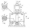
Figure 1 schematically depicts a lithographic apparatus. The apparatus comprises: - an illumination system (illuminator) IL configured to condition a radiation beam B (e.g. UV radiation or DUV radiation).
- a support structure (e.g. a mask table) MT constructed to support a patterning device (e.g. a mask) MA and connected to a first positioner PM configured to accurately position the patterning device in accordance with certain parameters;
- a substrate table (e.g. a wafer table) WT constructed to hold a substrate (e.g. a resist-coated wafer) W and connected to a second positioner PW configured to accurately position the substrate in accordance with certain parameters; and
- a projection system (e.g. a refractive projection lens system) PS configured to project a pattern imparted to the radiation beam B by patterning device MA onto a target portion C (e.g. comprising one or more dies) of the substrate W.
- The illumination system may include various types of optical components, such as refractive, reflective, magnetic, electromagnetic, electrostatic or other types of optical components, or any combination thereof, for directing, shaping, or controlling radiation.
- The support structure supports, i.e. bears the weight of, the patterning device. It holds the patterning device in a manner that depends on the orientation of the patterning device, the design of the lithographic apparatus, and other conditions, such as for example whether or not the patterning device is held in a vacuum environment. The support structure can use mechanical, vacuum, electrostatic or other clamping techniques to hold the patterning device. The support structure may be a frame or a table, for example, which may be fixed or movable as required. The support structure may ensure that the patterning device is at a desired position, for example with respect to the projection system. Any use of the terms "reticle" or "mask" herein may be considered synonymous with the more general term "patterning device."
- The term "patterning device" used herein should be broadly interpreted as referring to any device that can be used to impart a radiation beam with a pattern in its cross-section such as to create a pattern in a target portion of the substrate. It should be noted that the pattern imparted to the radiation beam may not exactly correspond to the desired pattern in the target portion of the substrate, for example if the pattern includes phase-shifting features or so called assist features. Generally, the pattern imparted to the radiation beam will correspond to a particular functional layer in a device being created in the target portion, such as an integrated circuit.
- The patterning device may be transmissive or reflective. Examples of patterning devices include masks, programmable mirror arrays, and programmable LCD panels. Masks are well known in lithography, and include mask types such as binary, alternating phase-shift, and attenuated phase-shift, as well as various hybrid mask types. An example of a programmable mirror array employs a matrix arrangement of small mirrors, each of which can be individually tilted so as to reflect an incoming radiation beam in different directions. The tilted mirrors impart a pattern in a radiation beam which is reflected by the mirror matrix.
- The term "projection system" used herein should be broadly interpreted as encompassing any type of projection system, including refractive, reflective, catadioptric, magnetic, electromagnetic and electrostatic optical systems, or any combination thereof, as appropriate for the exposure radiation being used, or for other factors such as the use of an immersion liquid or the use of a vacuum. Any use of the term "projection lens" herein may be considered as synonymous with the more general term "projection system".
- As here depicted, the apparatus is of a transmissive type (e.g. employing a transmissive mask). Alternatively, the apparatus may be of a reflective type (e.g. employing a programmable mirror array of a type as referred to above, or employing a reflective mask).
- The lithographic apparatus may be of a type having two (dual stage) or more substrate tables (and/or two or more mask tables). In such "multiple stage" machines the additional tables may be used in parallel, or preparatory steps may be carried out on one or more tables while one or more other tables are being used for exposure.
- Referring to
Figure 1 , the illuminator IL receives a radiation beam from a radiation source SO. The source and the lithographic apparatus may be separate entities, for example when the source is an excimer laser. In such cases, the source is not considered to form part of the lithographic apparatus and the radiation beam is passed from the source SO to the illuminator IL with the aid of a beam delivery system BD comprising, for example, suitable directing mirrors and/or a beam expander. In other cases the source may be an integral part of the lithographic apparatus, for example when the source is a mercury lamp. The source SO and the illuminator IL, together with the beam delivery system BD if required, may be referred to as a radiation system. - The illuminator IL may comprise an adjuster AD for adjusting the angular intensity distribution of the radiation beam. Generally, at least the outer and/or inner radial extent (commonly referred to as σ-outer and σ-inner, respectively) of the intensity distribution in a pupil plane of the illuminator can be adjusted. In addition, the illuminator IL may comprise various other components, such as an integrator IN and a condenser CO. The illuminator may be used to condition the radiation beam, to have a desired uniformity and intensity distribution in its cross-section.
- The radiation beam B is incident on the patterning device (e.g., mask MA), which is held on the support structure (e.g., mask table MT), and is patterned by the patterning device. Having traversed the mask MA, the radiation beam B passes through the projection system PS, which focuses the beam onto a target portion C of the substrate W. With the aid of the second positioner PW and position sensor IF (e.g. an interferometric device, linear encoder or capacitive sensor), the substrate table WT can be moved accurately, e.g. so as to position different target portions C in the path of the radiation beam B. Similarly, the first positioner PM and another position sensor (which is not explicitly depicted in
Figure 1 ) can be used to accurately position the mask MA with respect to the path of the radiation beam B, e.g. after mechanical retrieval from a mask library, or during a scan. In general, movement of the mask table MT may be realized with the aid of a long-stroke module (coarse positioning) and a short-stroke module (fine positioning), which form part of the first positioner PM. Similarly, movement of the substrate table WT may be realized using a long-stroke module and a short-stroke module, which form part of the second positioner PW. In the case of a stepper (as opposed to a scanner) the mask table MT may be connected to a short-stroke actuator only, or may be fixed. Mask MA and substrate W may be aligned using mask alignment marks M1, M2 and substrate alignment marks P1, P2. Although the substrate alignment marks as illustrated occupy dedicated target portions, they may be located in spaces between target portions (these are known as scribe-lane alignment marks). Similarly, in situations in which more than one die is provided on the mask MA, the mask alignment marks may be located between the dies. - The depicted apparatus could be used in at least one of the following modes:
- 1. In step mode, the mask table MT and the substrate table WT are kept essentially stationary, while an entire pattern imparted to the radiation beam is projected onto a target portion C at one time (i.e. a single static exposure). The substrate table WT is then shifted in the X and/or Y direction so that a different target portion C can be exposed. In step mode, the maximum size of the exposure field limits the size of the target portion C imaged in a single static exposure.
- 2. In scan mode, the mask table MT and the substrate table WT are scanned synchronously while a pattern imparted to the radiation beam is projected onto a target portion C (i.e. a single dynamic exposure). The velocity and direction of the substrate table WT relative to the mask table MT may be determined by the (de-)magnification and image reversal characteristics of the projection system PS. In scan mode, the maximum size of the exposure field limits the width (in the non-scanning direction) of the target portion in a single dynamic exposure, whereas the length of the scanning motion determines the height (in the scanning direction) of the target portion.
- 3. In another mode, the mask table MT is kept essentially stationary holding a programmable patterning device, and the substrate table WT is moved or scanned while a pattern imparted to the radiation beam is projected onto a target portion C. In this mode, generally a pulsed radiation source is employed and the programmable patterning device is updated as required after each movement of the substrate table WT or in between successive radiation pulses during a scan. This mode of operation can be readily applied to maskless lithography that utilizes programmable patterning device, such as a programmable mirror array of a type as referred to above.
- Combinations and/or variations on the above described modes of use or entirely different modes of use may also be employed.
-
Figure 5 shows aliquid reservoir 10 between the projection system PL and a substrate W which is positioned on the substrate stage WT. Theliquid reservoir 10 is filled with a liquid 11 having a relatively high refractive index, e.g. water, provided via inlet/outlet ducts 13. The liquid has the effect that the radiation of the projection beam is a shorter wavelength in the liquid than in air or in a vacuum, allowing smaller features to be resolved. It is well known that the resolution limit of a projection system is determined, inter alia, by the wavelength of the projection beam and the numerical aperture of the system. The presence of the liquid may also be regarded as increasing the effective numerical aperture. Furthermore, at fixed numerical aperture, the liquid is effective to increase the depth of field. - The
reservoir 10 forms a preferably contactless seal to the substrate W around the image field of the projection lens PL so that the liquid is confined to fill the space between the substrate's primary surface, which faces the projection system PL, and the final element (e.g. an 'abschlussplatte' which seals the projection system, or the final optical element of the projection system) of the projection system PL. The reservoir is formed by aseal member 12 positioned below and surrounding the final element of the projection lens PL. Thus, the liquid containment system LCS provides liquid on only a localized area of the substrate. Theseal member 12 forms part of the liquid containment system LCS for filling the space between the final element of the projection system and the sensor 10 (or substrate W) with a liquid. This liquid is brought into the space below the projection lens and within theseal member 12. Theseal member 12 extends a little above the bottom element of the projection lens and the liquid rises above the final element so that a buffer of liquid is provided. Theseal member 12 has an inner periphery that at the upper end closely conforms to the shape of the projection system or the final element thereof and may, e.g. be round. At the bottom the inner periphery forms an aperture which closely conforms to the shape of the image field, e.g. rectangular, though this is not necessarily so. The projection beam passes through this aperture. - The liquid 11 is confined in the
reservoir 10 by aseal device 16. As illustrated inFigure 5 , the seal device is a contactless seal, i.e. a gas seal. The gas seal is formed by gas, e.g. air or synthetic air, provided under pressure viainlet 15 to the gap betweenseal member 12 and substrate W and extracted byfirst outlet 14. The over pressure on thegas inlet 15, vacuum level on thefirst outlet 14 and the geometry of the gap are arranged so that there is a high-velocity air flow inwards towards the optical axis of the apparatus that confines the liquid 11. As with any seal, some liquid is likely to escape, for example up thefirst outlet 14. -
Figures 2 and 3 also depict a liquid reservoir defined by inlet(s) IN, outlet(s) OUT, the substrate W and the final element of projection lens PL. Like the liquid containment system ofFigure 5 the liquid containment system illustrated inFigures 2 and 3 , comprising inlet(s) IN and outlet(s) OUT, supplies liquid to a space between the final element of the projection system and a localized area of the primary surface of the substrate. - Both of the liquid containment systems LCS of
Figures 2 & 3 and Figure 4 as well as other solutions, such as a bath in which the substrate W or whole substrate table WT is immersed, can be used with the present invention described below. -
Figure 6 illustrates in detail thefinal element 20 of the projection system PL. In the example illustrated inFigure 6 the final element is a finaloptical element 20 which comprises afirst component 25 and asecond component 27. Thefinal element 20 of the projection system PL is comprised of first andsecond components - By providing the
final element 20 as first and second components or parts, the birefringence exhibited by CaF2 at 157 nm can be compensated for by ensuring that the crystal orientations of the first and second components are aligned such that the intrinsic birefringence exhibited by thefirst component 25 is cancelled by the intrinsic birefringence exhibited by thesecond component 27. In this way, the projection PB which passes first through thefirst component 25 and then through thesecond component 27 exits thesecond component 27 substantially free of birefringence phenomena. - The remaining optical elements of the projection system PL may be comprised of materials other than CaF2. The intensity of the projection beam is highest at the last element which is also the smallest so that it is this element which is most likely to suffer from compaction if made of quartz.
- As illustrated in
Figure 6 , thefinal element 20 of the projection system PL is substantially hemispherical in shape. Thus, thesecond component 27 is in the shape of a hemisphere and is positioned in a recess of thefirst component 25 which has an outer surface of the shape of a hemisphere with a recess in its non-curved surface. - It is has been found that CaF2 may dissolve or react with
immersion liquid 11 used in an immersion liquid lithographic projection apparatus. Presently the immersion liquid is envisaged as comprising substantially water for 248 and 193nm. For 157nm, perfluouro-hydrocarbons are envisaged. - One way of protecting the
final element 20 of the projection system from attack by the immersion liquid 11 (which is not in accordance with the present invention) is to provide aprotective coating 40 on a surface of thefinal element 20 which is in contact with the immersion liquid. The material of theprotective coating 40 is preferably inert in theimmersion liquid 11 and does not dissolve. As is illustrated inFigure 6 , theprotective coating 40 is attached to the bottom (as illustrated) surface of thesecond component 27 of the projection system PL. - It is preferable to make the protective layer as thin as possible while still providing protection to the final
optical element 20 of the projection system PL. The protective coating is preferably between 5 and 500 nm thick, more preferably between 10 and 200 nm thick. Preferably material of theprotective coating 40 is a metal, a metal oxide or nitride or SiO2 with a low contact angle with the immersion fluid to limit bubble inclusion. The layer may be deposited on theelement 20 by e.g. evaporation, sputtering etc. - The use of a
protective coating 40 is not limited to the case where thefinal element 20 of the projection system PL is comprised of CaF2. For example, if the final element is comprised of quartz (as typically in the case of an abschlussplatte being the final element), there may also be problems due to the dissolution or reaction of quartz with theimmersion liquid 11. In this case aprotective layer 40 may also be required. - The
protective coating 40 should be as thin as possible to minimize transmission losses. The refractive index of theprotective coating 40 can be partially varied by the deposition process and the deposition parameters. Experience gained in the deposition of EUV coatings might be usefully harnessed to optimize this process. - In an embodiment of the invention, shown in
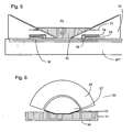
Figure 7 , thefinal element 20 of the projection system is protected by a fusedsilica plate 45. This plate has a thickness in the range of from 50µm to 5mm and is contact bonded to thefinal element 20. In contact bonding, no glue is used - the bonding surfaces are made smooth and clean enough to directly bond together. After bonding to the final element, the fused silica plate may be ground and polished to the desired thickness, avoiding difficulties inherent in handling a very thin plate. A liquid-tight seal 46 may be provided around the perimeter of the join. - A
seal 46 around the join of the final element and the fused silica protective plate is especially desirable where the final element and fused silica plate are contact bonded together. Although this form of bonding can provide an exceptionally strong bond, where dissimilar materials, such as CaF and fused silica, are bonded temperature changes and thermal gradients can cause the bond to "breathe" - differential thermal expansion or contraction of the two materials causes them to separate until the stress is relieved. Although the bond usually reforms very quickly in the case of thermal separation, if this occurs when the final element is in contact with a liquid, e.g. during polishing or grinding of the protective layer or use of the apparatus, liquid can be drawn into the gap. - One form of seal that may be used is a layer of SiO formed by applying a suitable precursor (such as silicone fluids (i.e. comprising Si-O chains of various lengths with various hydrocarbon side-chains), tetraethyl orthosilicate, decamethyl tetrasiloxane and tetrabutyl orthosilicate) and irradiating it with DUV light to photo-convert the precursor to SiO. This form of seal has the advantage that it has a similar hardness to the fused silica plate and so polishes at a similar rate.
- Another form of seal that is useful is a silicon caulk provided over a layer of titanium oxide. The titanium oxide is applied by painting a precursor onto the seal and photo-converting it to titanium oxide and acts to protect the silicone caulk from UV light during operation of the apparatus.
- A further form of seal is formed by painting tetraethyl orthosilicate around the join, which then decomposes at room temperature to form a thin layer of fused silica which forms a seal. This seal is however rather brittle so that careful handling is required.
- In a variant of the
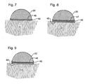
Figure 7 arrangement shown inFigure 8 , a liquid 47, such as oil, is provided between thelast lens element 20 and theprotective plate 45. The liquid 47 preferably has a refractive index as close as possible to that of theimmersion fluid 11, which may be water, but is not damaging to the material of thefinal lens element 20, which may be CaF2. This enables the protective plate to be interchangeable by substantially reducing the requirements on the accuracy with which theprotective plate 45 must be positioned as the fluids above and below it have similar refractive indexes. - A further variant, shown in
Figure 9 , uses a two layer protective coating, made up ofinner layer 48 andouter layer 49. It can be very difficult to form a layer of protective coating, without pinholes. Even the smallest pinhole in a protective coating applied to a CaF body allows dissolution of the CaF body when immersed in water, causing cavitation which is extremely deleterious to the optical properties of the element. By the use of a two layer protective coating, it can be arranged that the pinholes in one layer do not match up with the pinholes in the other layer so that there is no through path in the protective layer. It can best be ensured that the pinholes of the two layers do not match up by applying the two protective layers by different methods. - In an example a
first layer 48 of SiO is applied by sputtering and asecond layer 49 is applied by spin coating a precursor and photo-converting the precursor to SiO. This method has been found to be more effective than sputtering two layers of SiO since the pinholes in the second sputtered layer have a tendency to line up with those in the first layer. Surprisingly, it has been found that the spin coating and photo-conversion method provides a layer of bulk SiO rather than porous SiO. A layer formed by spin-coating a precursor and then photo-converting it to SiO may also be used on its own as a seal layer. - The precursor used to form
protective layer 49 may be any suitable fluid of, or containing, organo-silicon compounds. Suitable examples are silicone fluids (i.e. comprising Si-O chains of various lengths with various hydrocarbon side-chains), tetraethyl orthosilicate, decamethyl tetrasiloxane and tetrabutyl orthosilicate. The material may be chosen to have a desired viscosity to enable a suitably even layer to be provided by spin coating. Solvents, preferably volatile organic solvents, may be used to adjust the viscosity if necessary. - Photo-conversion of the precursor to SiO can be achieved with irradiation by DUV light of various wavelengths, e.g. 184nm or 172nm, at a rate determined to avoid any deleterious effects that might be induced by thermal gradients in the element.
- Each of the two layers of the protective coating may have a thickness in the range of 50 to 200nm.
- Although specific reference may be made in this text to the use of lithographic apparatus in the manufacture of ICs, it should be understood that the lithographic apparatus described herein may have other applications, such as the manufacture of integrated optical systems, guidance and detection patterns for magnetic domain memories, flat-panel displays, liquid-crystal displays (LCDs), thin-film magnetic heads, etc. The skilled artisan will appreciate that, in the context of such alternative applications, any use of the terms "wafer" or "die" herein may be considered as synonymous with the more general terms "substrate" or "target portion", respectively. The substrate referred to herein may be processed, before or after exposure, in for example a track (a tool that typically applies a layer of resist to a substrate and develops the exposed resist), a metrology tool and/or an inspection tool. Where applicable, the disclosure herein may be applied to such and other substrate processing tools. Further, the substrate may be processed more than once, for example in order to create a multi-layer IC, so that the term substrate used herein may also refer to a substrate that already contains multiple processed layers.
- The terms "radiation" and "beam" used herein encompass all types of electromagnetic radiation, including ultraviolet (UV) radiation (e.g. having a wavelength of or about 365, 248, 193, 157 or 126 nm).
- The term "lens", where the context allows, may refer to any one or combination of various types of optical components, including refractive and reflective optical components.
- While specific embodiments of the invention have been described above, it will be appreciated that the invention may be practiced otherwise than as described.
- The present invention can be applied to any immersion lithography apparatus, in particular, but not exclusively, those types mentioned above.
- The descriptions above are intended to be illustrative, not limiting. Thus, it will be apparent to one skilled in the art that modifications may be made to the invention as described without departing from the scope of the claims set out below which define the invention.
Claims (5)
- A lithographic projection apparatus comprising:a projection system (PL) arranged to project a pattern from a patterning device (MA) onto a substrate (W); anda liquid supply system for at least partly filling a space between a final element (20) of said projection system (PL) and said substrate (W) with an immersion liquid (11),wherein said final element (20) has, on a surface in contact with said immersion liquid (11), a protective material which is substantially insoluble in said immersion liquid (11),wherein said protective material is a fused silica plate (45), said fused silica plate (45) is attached to said final element (20) by contact bonding without glue, wherein said fused silica plate (45) has a thickness in the range of from 50µm to 5mm.
- A lithographic projection apparatus according to claim 1, wherein the lithographic projection apparatus is provided with a liquid tight seal (46) around the perimeter of a join between the final element (20) and the fused silica plate (45).
- A lithographic projection apparatus according to any one of the preceding claims, wherein said final element (20) is comprised of CaF2.
- A lithographic projection apparatus according to claim 3, wherein said final element(20) is comprised of a first and a second component (25,27), both components (25,27) being of CaF2, wherein said projection beam passes through said first component (25) before passing through said second component (27).
- A device manufacturing method comprising projecting a patterned beam of radiation onto a substrate (W) through an immersion liquid (11) provided in a space between a final element (20) of a projection system (PL) and said substrate (W), wherein a protective fused silica plate (45) which is substantially insoluble in said immersion liquid (11) is provided on said final element (20) on a surface thereof in contact with said immersion liquid (11),
wherein said fused silica plate (45) is attached to said final element (20) by contact bonding without glue, wherein said fused silica plate (45) has a thickness in the range of from 50µm to 5mm.
Priority Applications (2)
| Application Number | Priority Date | Filing Date | Title |
|---|---|---|---|
| EP10179586.2A EP2261740B1 (en) | 2003-08-29 | 2004-08-17 | Lithographic apparatus |
| EP04254940A EP1510871B1 (en) | 2003-08-29 | 2004-08-17 | Lithographic apparatus and device manufacturing method |
Applications Claiming Priority (4)
| Application Number | Priority Date | Filing Date | Title |
|---|---|---|---|
| EP03255377 | 2003-08-29 | ||
| EP03255377 | 2003-08-29 | ||
| US10/698,012 US6954256B2 (en) | 2003-08-29 | 2003-10-31 | Gradient immersion lithography |
| EP04254940A EP1510871B1 (en) | 2003-08-29 | 2004-08-17 | Lithographic apparatus and device manufacturing method |
Related Child Applications (2)
| Application Number | Title | Priority Date | Filing Date |
|---|---|---|---|
| EP10179586.2A Division EP2261740B1 (en) | 2003-08-29 | 2004-08-17 | Lithographic apparatus |
| EP10179586.2 Division-Into | 2010-09-24 |
Publications (3)
| Publication Number | Publication Date |
|---|---|
| EP1510871A2 EP1510871A2 (en) | 2005-03-02 |
| EP1510871A3 EP1510871A3 (en) | 2005-04-06 |
| EP1510871B1 true EP1510871B1 (en) | 2012-04-04 |
Family
ID=34424773
Family Applications (1)
| Application Number | Title | Priority Date | Filing Date |
|---|---|---|---|
| EP04254940A Not-in-force EP1510871B1 (en) | 2003-08-29 | 2004-08-17 | Lithographic apparatus and device manufacturing method |
Country Status (5)
| Country | Link |
|---|---|
| US (2) | US6954256B2 (en) |
| EP (1) | EP1510871B1 (en) |
| JP (3) | JP3946212B2 (en) |
| CN (1) | CN100495213C (en) |
| SG (1) | SG109610A1 (en) |
Families Citing this family (248)
| Publication number | Priority date | Publication date | Assignee | Title |
|---|---|---|---|---|
| JP2005536775A (en) * | 2002-08-23 | 2005-12-02 | 株式会社ニコン | Projection optical system, photolithography method and exposure apparatus, and method using exposure apparatus |
| US7081278B2 (en) * | 2002-09-25 | 2006-07-25 | Asml Holdings N.V. | Method for protection of adhesives used to secure optics from ultra-violet light |
| SG121822A1 (en) * | 2002-11-12 | 2006-05-26 | Asml Netherlands Bv | Lithographic apparatus and device manufacturing method |
| CN100470367C (en) | 2002-11-12 | 2009-03-18 | Asml荷兰有限公司 | Lithographic apparatus and device manufacturing method |
| US9482966B2 (en) | 2002-11-12 | 2016-11-01 | Asml Netherlands B.V. | Lithographic apparatus and device manufacturing method |
| US10503084B2 (en) | 2002-11-12 | 2019-12-10 | Asml Netherlands B.V. | Lithographic apparatus and device manufacturing method |
| US7110081B2 (en) | 2002-11-12 | 2006-09-19 | Asml Netherlands B.V. | Lithographic apparatus and device manufacturing method |
| JP3953460B2 (en) | 2002-11-12 | 2007-08-08 | エーエスエムエル ネザーランズ ビー.ブイ. | Lithographic projection apparatus |
| US7372541B2 (en) * | 2002-11-12 | 2008-05-13 | Asml Netherlands B.V. | Lithographic apparatus and device manufacturing method |
| DE60335595D1 (en) | 2002-11-12 | 2011-02-17 | Asml Netherlands Bv | Immersion lithographic apparatus and method of making a device |
| KR20050085235A (en) * | 2002-12-10 | 2005-08-29 | 가부시키가이샤 니콘 | Exposure system and device producing method |
| SG171468A1 (en) * | 2002-12-10 | 2011-06-29 | Nikon Corp | Exposure apparatus and method for producing device |
| CN1723541B (en) | 2002-12-10 | 2010-06-02 | 株式会社尼康 | Exposure apparatus and method for producing device |
| JP4352874B2 (en) * | 2002-12-10 | 2009-10-28 | 株式会社ニコン | Exposure apparatus and device manufacturing method |
| US7242455B2 (en) * | 2002-12-10 | 2007-07-10 | Nikon Corporation | Exposure apparatus and method for producing device |
| KR20050085026A (en) | 2002-12-10 | 2005-08-29 | 가부시키가이샤 니콘 | Optical device and projection exposure apparatus using such optical device |
| KR101101737B1 (en) * | 2002-12-10 | 2012-01-05 | 가부시키가이샤 니콘 | Exposure apparatus, exposure method and method for manufacturing device |
| US7948604B2 (en) * | 2002-12-10 | 2011-05-24 | Nikon Corporation | Exposure apparatus and method for producing device |
| EP1579435B1 (en) | 2002-12-19 | 2007-06-27 | Koninklijke Philips Electronics N.V. | Method and device for irradiating spots on a layer |
| DE10261775A1 (en) * | 2002-12-20 | 2004-07-01 | Carl Zeiss Smt Ag | Device for the optical measurement of an imaging system |
| KR101562447B1 (en) | 2003-02-26 | 2015-10-21 | 가부시키가이샤 니콘 | Exposure apparatus and method, and method of producing apparatus |
| WO2004086470A1 (en) | 2003-03-25 | 2004-10-07 | Nikon Corporation | Exposure system and device production method |
| EP1612850B1 (en) | 2003-04-07 | 2009-03-25 | Nikon Corporation | Exposure apparatus and method for manufacturing a device |
| KR20110104084A (en) * | 2003-04-09 | 2011-09-21 | 가부시키가이샤 니콘 | Immersion lithography fluid control system |
| SG141426A1 (en) | 2003-04-10 | 2008-04-28 | Nikon Corp | Environmental system including vacuum scavange for an immersion lithography apparatus |
| EP3352015A1 (en) | 2003-04-10 | 2018-07-25 | Nikon Corporation | Environmental system including a transport region for an immersion lithography apparatus |
| WO2004090633A2 (en) * | 2003-04-10 | 2004-10-21 | Nikon Corporation | An electro-osmotic element for an immersion lithography apparatus |
| JP4488005B2 (en) * | 2003-04-10 | 2010-06-23 | 株式会社ニコン | Outflow passage for collecting liquid for an immersion lithographic apparatus |
| SG2014015135A (en) * | 2003-04-11 | 2015-06-29 | Nippon Kogaku Kk | Cleanup method for optics in immersion lithography |
| CN101980087B (en) | 2003-04-11 | 2013-03-27 | 株式会社尼康 | Immersion exposure appratus and method |
| WO2004092830A2 (en) | 2003-04-11 | 2004-10-28 | Nikon Corporation | Liquid jet and recovery system for immersion lithography |
| JP2006523958A (en) | 2003-04-17 | 2006-10-19 | 株式会社ニコン | Optical structure of an autofocus element for use in immersion lithography |
| KR101516142B1 (en) | 2003-05-06 | 2015-05-04 | 가부시키가이샤 니콘 | Projection optical system, and exposure apparatus and exposure method |
| US7348575B2 (en) | 2003-05-06 | 2008-03-25 | Nikon Corporation | Projection optical system, exposure apparatus, and exposure method |
| TWI295414B (en) | 2003-05-13 | 2008-04-01 | Asml Netherlands Bv | Lithographic apparatus and device manufacturing method |
| JP4552853B2 (en) * | 2003-05-15 | 2010-09-29 | 株式会社ニコン | Exposure apparatus and device manufacturing method |
| TW201515064A (en) | 2003-05-23 | 2015-04-16 | 尼康股份有限公司 | Exposure device, exposure method, and device manufacturing method |
| TWI612556B (en) * | 2003-05-23 | 2018-01-21 | Nikon Corp | Exposure apparatus, exposure method, and component manufacturing method |
| CN100541717C (en) * | 2003-05-28 | 2009-09-16 | 株式会社尼康 | Exposure method, exposure device and device making method |
| TWI347741B (en) * | 2003-05-30 | 2011-08-21 | Asml Netherlands Bv | Lithographic apparatus and device manufacturing method |
| US7213963B2 (en) | 2003-06-09 | 2007-05-08 | Asml Netherlands B.V. | Lithographic apparatus and device manufacturing method |
| US7317504B2 (en) * | 2004-04-08 | 2008-01-08 | Asml Netherlands B.V. | Lithographic apparatus and device manufacturing method |
| US7684008B2 (en) | 2003-06-11 | 2010-03-23 | Asml Netherlands B.V. | Lithographic apparatus and device manufacturing method |
| TW201818451A (en) | 2003-06-13 | 2018-05-16 | 日商尼康股份有限公司 | Substrate stage, exposure device |
| KR101674329B1 (en) | 2003-06-19 | 2016-11-08 | 가부시키가이샤 니콘 | Exposure device and device producing method |
| US7236232B2 (en) * | 2003-07-01 | 2007-06-26 | Nikon Corporation | Using isotopically specified fluids as optical elements |
| EP2466382B1 (en) * | 2003-07-08 | 2014-11-26 | Nikon Corporation | Wafer table for immersion lithography |
| WO2005006418A1 (en) * | 2003-07-09 | 2005-01-20 | Nikon Corporation | Exposure apparatus and method for manufacturing device |
| EP2264532B1 (en) * | 2003-07-09 | 2012-10-31 | Nikon Corporation | Exposure apparatus and device manufacturing method |
| KR20060026883A (en) * | 2003-07-09 | 2006-03-24 | 가부시키가이샤 니콘 | Linking unit, exposure apparatus and method for manufacturing device |
| US7738074B2 (en) | 2003-07-16 | 2010-06-15 | Asml Netherlands B.V. | Lithographic apparatus and device manufacturing method |
| EP1500982A1 (en) | 2003-07-24 | 2005-01-26 | ASML Netherlands B.V. | Lithographic apparatus and device manufacturing method |
| WO2005010960A1 (en) * | 2003-07-25 | 2005-02-03 | Nikon Corporation | Inspection method and inspection device for projection optical system, and production method for projection optical system |
| EP1503244A1 (en) | 2003-07-28 | 2005-02-02 | ASML Netherlands B.V. | Lithographic projection apparatus and device manufacturing method |
| CN102043350B (en) | 2003-07-28 | 2014-01-29 | 株式会社尼康 | Exposure apparatus, device manufacturing method, and control method of exposure apparatus |
| US7175968B2 (en) * | 2003-07-28 | 2007-02-13 | Asml Netherlands B.V. | Lithographic apparatus, device manufacturing method and a substrate |
| US7326522B2 (en) | 2004-02-11 | 2008-02-05 | Asml Netherlands B.V. | Device manufacturing method and a substrate |
| US7779781B2 (en) | 2003-07-31 | 2010-08-24 | Asml Netherlands B.V. | Lithographic apparatus and device manufacturing method |
| US8149381B2 (en) * | 2003-08-26 | 2012-04-03 | Nikon Corporation | Optical element and exposure apparatus |
| SG133590A1 (en) * | 2003-08-26 | 2007-07-30 | Nikon Corp | Optical element and exposure device |
| EP2804048A1 (en) * | 2003-08-29 | 2014-11-19 | Nikon Corporation | Exposure apparatus and device fabricating method |
| TWI245163B (en) | 2003-08-29 | 2005-12-11 | Asml Netherlands Bv | Lithographic apparatus and device manufacturing method |
| EP2261740B1 (en) | 2003-08-29 | 2014-07-09 | ASML Netherlands BV | Lithographic apparatus |
| US6954256B2 (en) | 2003-08-29 | 2005-10-11 | Asml Netherlands B.V. | Gradient immersion lithography |
| TWI263859B (en) | 2003-08-29 | 2006-10-11 | Asml Netherlands Bv | Lithographic apparatus and device manufacturing method |
| KR101238114B1 (en) | 2003-09-03 | 2013-02-27 | 가부시키가이샤 니콘 | Apparatus and method for providing fluid for immersion lithography |
| WO2005029559A1 (en) * | 2003-09-19 | 2005-03-31 | Nikon Corporation | Exposure apparatus and device producing method |
| EP1670042A4 (en) * | 2003-09-29 | 2008-01-30 | Nikon Corp | Liquid immersion type lens system and projection aligner, device production method |
| TW200518187A (en) | 2003-09-29 | 2005-06-01 | Nikon Corp | Exposure apparatus, exposure method, and device manufacturing method |
| US7369217B2 (en) * | 2003-10-03 | 2008-05-06 | Micronic Laser Systems Ab | Method and device for immersion lithography |
| EP1672681B8 (en) | 2003-10-08 | 2011-09-21 | Miyagi Nikon Precision Co., Ltd. | Exposure apparatus, substrate carrying method, exposure method, and method for producing device |
| JP2005136364A (en) * | 2003-10-08 | 2005-05-26 | Zao Nikon Co Ltd | Substrate carrying device, exposure device and device manufacturing method |
| EP1672682A4 (en) | 2003-10-08 | 2008-10-15 | Zao Nikon Co Ltd | Substrate transporting apparatus and method, exposure apparatus and method, and device producing method |
| TW201738932A (en) * | 2003-10-09 | 2017-11-01 | Nippon Kogaku Kk | Exposure apparatus, exposure method, and device producing method |
| EP1524558A1 (en) * | 2003-10-15 | 2005-04-20 | ASML Netherlands B.V. | Lithographic apparatus and device manufacturing method |
| EP1524557A1 (en) * | 2003-10-15 | 2005-04-20 | ASML Netherlands B.V. | Lithographic apparatus and device manufacturing method |
| US7352433B2 (en) | 2003-10-28 | 2008-04-01 | Asml Netherlands B.V. | Lithographic apparatus and device manufacturing method |
| US7411653B2 (en) * | 2003-10-28 | 2008-08-12 | Asml Netherlands B.V. | Lithographic apparatus |
| US7924397B2 (en) * | 2003-11-06 | 2011-04-12 | Taiwan Semiconductor Manufacturing Company, Ltd. | Anti-corrosion layer on objective lens for liquid immersion lithography applications |
| JP4295712B2 (en) | 2003-11-14 | 2009-07-15 | エーエスエムエル ネザーランズ ビー.ブイ. | Lithographic apparatus and apparatus manufacturing method |
| US7545481B2 (en) | 2003-11-24 | 2009-06-09 | Asml Netherlands B.V. | Lithographic apparatus and device manufacturing method |
| KR101394764B1 (en) | 2003-12-03 | 2014-05-27 | 가부시키가이샤 니콘 | Exposure apparatus, exposure method, device producing method, and optical component |
| JP2005175034A (en) * | 2003-12-09 | 2005-06-30 | Canon Inc | Aligner |
| CN100487860C (en) * | 2003-12-15 | 2009-05-13 | 株式会社尼康 | Stage system, exposure apparatus and exposure method |
| US20070081133A1 (en) * | 2004-12-14 | 2007-04-12 | Niikon Corporation | Projection exposure apparatus and stage unit, and exposure method |
| JP2005189850A (en) * | 2003-12-15 | 2005-07-14 | Carl Zeiss Smt Ag | Refractive projection objective lens for immersion lithography |
| WO2005057635A1 (en) * | 2003-12-15 | 2005-06-23 | Nikon Corporation | Projection exposure apparatus, stage apparatus, and exposure method |
| JP4907596B2 (en) * | 2003-12-15 | 2012-03-28 | カール・ツァイス・エスエムティー・ゲーエムベーハー | Refractive projection objective |
| US7460206B2 (en) * | 2003-12-19 | 2008-12-02 | Carl Zeiss Smt Ag | Projection objective for immersion lithography |
| US7589818B2 (en) * | 2003-12-23 | 2009-09-15 | Asml Netherlands B.V. | Lithographic apparatus, alignment apparatus, device manufacturing method, and a method of converting an apparatus |
| US7394521B2 (en) * | 2003-12-23 | 2008-07-01 | Asml Netherlands B.V. | Lithographic apparatus and device manufacturing method |
| JP2005191394A (en) * | 2003-12-26 | 2005-07-14 | Canon Inc | Exposing method and equipment |
| JP2005195878A (en) * | 2004-01-07 | 2005-07-21 | Olympus Corp | Objective lens, optical analyzer, method of operating the optical analyzer, and microscope |
| ATE459898T1 (en) | 2004-01-20 | 2010-03-15 | Zeiss Carl Smt Ag | EXPOSURE DEVICE AND MEASURING DEVICE FOR A PROJECTION LENS |
| US20050161644A1 (en) * | 2004-01-23 | 2005-07-28 | Peng Zhang | Immersion lithography fluids |
| TWI259319B (en) * | 2004-01-23 | 2006-08-01 | Air Prod & Chem | Immersion lithography fluids |
| US7589822B2 (en) | 2004-02-02 | 2009-09-15 | Nikon Corporation | Stage drive method and stage unit, exposure apparatus, and device manufacturing method |
| KR101227211B1 (en) | 2004-02-03 | 2013-01-28 | 가부시키가이샤 니콘 | Exposure apparatus and method of producing device |
| US7050146B2 (en) | 2004-02-09 | 2006-05-23 | Asml Netherlands B.V. | Lithographic apparatus and device manufacturing method |
| JP4370992B2 (en) * | 2004-02-18 | 2009-11-25 | 株式会社ニコン | Optical element and exposure apparatus |
| TWI395069B (en) * | 2004-02-18 | 2013-05-01 | 尼康股份有限公司 | Projection optical system, exposure device and exposure method |
| JP4974049B2 (en) * | 2004-02-20 | 2012-07-11 | 株式会社ニコン | Exposure method, exposure apparatus, and device manufacturing method |
| KR101441777B1 (en) | 2004-03-25 | 2014-09-22 | 가부시키가이샤 니콘 | Exposure apparatus and method for manufacturing device |
| JP4510494B2 (en) * | 2004-03-29 | 2010-07-21 | キヤノン株式会社 | Exposure equipment |
| US7034917B2 (en) * | 2004-04-01 | 2006-04-25 | Asml Netherlands B.V. | Lithographic apparatus, device manufacturing method and device manufactured thereby |
| US7898642B2 (en) * | 2004-04-14 | 2011-03-01 | Asml Netherlands B.V. | Lithographic apparatus and device manufacturing method |
| US20050231695A1 (en) * | 2004-04-15 | 2005-10-20 | Taiwan Semiconductor Manufacturing Company, Ltd. | Method and system for immersion lithography using high PH immersion fluid |
| US7271878B2 (en) * | 2004-04-22 | 2007-09-18 | International Business Machines Corporation | Wafer cell for immersion lithography |
| EP1747499A2 (en) | 2004-05-04 | 2007-01-31 | Nikon Corporation | Apparatus and method for providing fluid for immersion lithography |
| US20060244938A1 (en) * | 2004-05-04 | 2006-11-02 | Karl-Heinz Schuster | Microlitographic projection exposure apparatus and immersion liquid therefore |
| US7616383B2 (en) * | 2004-05-18 | 2009-11-10 | Asml Netherlands B.V. | Lithographic apparatus and device manufacturing method |
| US7486381B2 (en) * | 2004-05-21 | 2009-02-03 | Asml Netherlands B.V. | Lithographic apparatus and device manufacturing method |
| US20070103661A1 (en) * | 2004-06-04 | 2007-05-10 | Nikon Corporation | Exposure apparatus, exposure method, and method for producing device |
| EP1768169B9 (en) * | 2004-06-04 | 2013-03-06 | Nikon Corporation | Exposure apparatus, exposure method, and device producing method |
| CN101833247B (en) | 2004-06-04 | 2013-11-06 | 卡尔蔡司Smt有限责任公司 | Measuring system for the optical measurement of projecting object lens of micro-lithography projection exposure system |
| JP4655763B2 (en) * | 2004-06-04 | 2011-03-23 | 株式会社ニコン | Exposure apparatus, exposure method, and device manufacturing method |
| KR101512884B1 (en) * | 2004-06-09 | 2015-04-16 | 가부시키가이샤 니콘 | Exposure system and device production method |
| US20070222959A1 (en) * | 2004-06-10 | 2007-09-27 | Nikon Corporation | Exposure apparatus, exposure method, and method for producing device |
| KR101700546B1 (en) | 2004-06-10 | 2017-01-26 | 가부시키가이샤 니콘 | Exposure apparatus, exposure method, and device producing method |
| US7481867B2 (en) | 2004-06-16 | 2009-01-27 | Edwards Limited | Vacuum system for immersion photolithography |
| US7180572B2 (en) * | 2004-06-23 | 2007-02-20 | Taiwan Semiconductor Manufacturing Company, Ltd. | Immersion optical projection system |
| US7463330B2 (en) | 2004-07-07 | 2008-12-09 | Asml Netherlands B.V. | Lithographic apparatus and device manufacturing method |
| ATE441937T1 (en) | 2004-07-12 | 2009-09-15 | Nikon Corp | EXPOSURE DEVICE AND COMPONENT PRODUCTION METHOD |
| US7304715B2 (en) | 2004-08-13 | 2007-12-04 | Asml Netherlands B.V. | Lithographic apparatus and device manufacturing method |
| KR20070048164A (en) * | 2004-08-18 | 2007-05-08 | 가부시키가이샤 니콘 | Exposure apparatus and device manufacturing method |
| US7701550B2 (en) | 2004-08-19 | 2010-04-20 | Asml Netherlands B.V. | Lithographic apparatus and device manufacturing method |
| US7522261B2 (en) * | 2004-09-24 | 2009-04-21 | Asml Netherlands B.V. | Lithographic apparatus and device manufacturing method |
| US7355674B2 (en) * | 2004-09-28 | 2008-04-08 | Asml Netherlands B.V. | Lithographic apparatus, device manufacturing method and computer program product |
| US7894040B2 (en) * | 2004-10-05 | 2011-02-22 | Asml Netherlands B.V. | Lithographic apparatus and device manufacturing method |
| US7379155B2 (en) * | 2004-10-18 | 2008-05-27 | Asml Netherlands B.V. | Lithographic apparatus and device manufacturing method |
| US7414699B2 (en) * | 2004-11-12 | 2008-08-19 | Asml Netherlands B.V. | Lithographic apparatus and device manufacturing method |
| US7423720B2 (en) | 2004-11-12 | 2008-09-09 | Asml Netherlands B.V. | Lithographic apparatus and device manufacturing method |
| US7583357B2 (en) * | 2004-11-12 | 2009-09-01 | Asml Netherlands B.V. | Lithographic apparatus and device manufacturing method |
| US7411657B2 (en) * | 2004-11-17 | 2008-08-12 | Asml Netherlands B.V. | Lithographic apparatus and device manufacturing method |
| US20070285634A1 (en) * | 2004-11-19 | 2007-12-13 | Nikon Corporation | Maintenance Method, Exposure Method, Exposure Apparatus, And Method For Producing Device |
| US7256121B2 (en) * | 2004-12-02 | 2007-08-14 | Texas Instruments Incorporated | Contact resistance reduction by new barrier stack process |
| US7161654B2 (en) * | 2004-12-02 | 2007-01-09 | Asml Netherlands B.V. | Lithographic apparatus and device manufacturing method |
| US7446850B2 (en) * | 2004-12-03 | 2008-11-04 | Asml Netherlands B.V. | Lithographic apparatus and device manufacturing method |
| US7196770B2 (en) * | 2004-12-07 | 2007-03-27 | Asml Netherlands B.V. | Prewetting of substrate before immersion exposure |
| US7397533B2 (en) | 2004-12-07 | 2008-07-08 | Asml Netherlands B.V. | Lithographic apparatus and device manufacturing method |
| US7365827B2 (en) | 2004-12-08 | 2008-04-29 | Asml Netherlands B.V. | Lithographic apparatus and device manufacturing method |
| US7352440B2 (en) | 2004-12-10 | 2008-04-01 | Asml Netherlands B.V. | Substrate placement in immersion lithography |
| US7403261B2 (en) * | 2004-12-15 | 2008-07-22 | Asml Netherlands B.V. | Lithographic apparatus and device manufacturing method |
| US7528931B2 (en) | 2004-12-20 | 2009-05-05 | Asml Netherlands B.V. | Lithographic apparatus and device manufacturing method |
| US7880860B2 (en) * | 2004-12-20 | 2011-02-01 | Asml Netherlands B.V. | Lithographic apparatus and device manufacturing method |
| US7491661B2 (en) * | 2004-12-28 | 2009-02-17 | Asml Netherlands B.V. | Device manufacturing method, top coat material and substrate |
| US7405805B2 (en) * | 2004-12-28 | 2008-07-29 | Asml Netherlands B.V. | Lithographic apparatus and device manufacturing method |
| US20060147821A1 (en) | 2004-12-30 | 2006-07-06 | Asml Netherlands B.V. | Lithographic apparatus and device manufacturing method |
| US7450217B2 (en) * | 2005-01-12 | 2008-11-11 | Asml Netherlands B.V. | Exposure apparatus, coatings for exposure apparatus, lithographic apparatus, device manufacturing method, and device manufactured thereby |
| SG124351A1 (en) | 2005-01-14 | 2006-08-30 | Asml Netherlands Bv | Lithographic apparatus and device manufacturing method |
| SG124359A1 (en) | 2005-01-14 | 2006-08-30 | Asml Netherlands Bv | Lithographic apparatus and device manufacturing method |
| US8692973B2 (en) * | 2005-01-31 | 2014-04-08 | Nikon Corporation | Exposure apparatus and method for producing device |
| EP3079164A1 (en) * | 2005-01-31 | 2016-10-12 | Nikon Corporation | Exposure apparatus and method for producing device |
| JP2006222222A (en) * | 2005-02-09 | 2006-08-24 | Canon Inc | Projection optical system and exposure apparatus having the same |
| CN101128775B (en) | 2005-02-10 | 2012-07-25 | Asml荷兰有限公司 | Immersion liquid, exposure apparatus, and exposure process |
| US7378025B2 (en) * | 2005-02-22 | 2008-05-27 | Asml Netherlands B.V. | Fluid filtration method, fluid filtered thereby, lithographic apparatus and device manufacturing method |
| US7224431B2 (en) * | 2005-02-22 | 2007-05-29 | Asml Netherlands B.V. | Lithographic apparatus and device manufacturing method |
| US8018573B2 (en) | 2005-02-22 | 2011-09-13 | Asml Netherlands B.V. | Lithographic apparatus and device manufacturing method |
| US7428038B2 (en) | 2005-02-28 | 2008-09-23 | Asml Netherlands B.V. | Lithographic apparatus, device manufacturing method and apparatus for de-gassing a liquid |
| US7282701B2 (en) | 2005-02-28 | 2007-10-16 | Asml Netherlands B.V. | Sensor for use in a lithographic apparatus |
| US7324185B2 (en) | 2005-03-04 | 2008-01-29 | Asml Netherlands B.V. | Lithographic apparatus and device manufacturing method |
| US7684010B2 (en) * | 2005-03-09 | 2010-03-23 | Asml Netherlands B.V. | Lithographic apparatus, device manufacturing method, seal structure, method of removing an object and a method of sealing |
| JP2006261606A (en) * | 2005-03-18 | 2006-09-28 | Canon Inc | Exposure device, exposure method and device manufacturing method |
| US7330238B2 (en) * | 2005-03-28 | 2008-02-12 | Asml Netherlands, B.V. | Lithographic apparatus, immersion projection apparatus and device manufacturing method |
| US7411654B2 (en) | 2005-04-05 | 2008-08-12 | Asml Netherlands B.V. | Lithographic apparatus and device manufacturing method |
| US7291850B2 (en) * | 2005-04-08 | 2007-11-06 | Asml Netherlands B.V. | Lithographic apparatus and device manufacturing method |
| USRE43576E1 (en) | 2005-04-08 | 2012-08-14 | Asml Netherlands B.V. | Dual stage lithographic apparatus and device manufacturing method |
| US20090135382A1 (en) * | 2005-04-28 | 2009-05-28 | Nikon Corporation | Exposure method, exposure apparatus, and method for producing device |
| US7317507B2 (en) * | 2005-05-03 | 2008-01-08 | Asml Netherlands B.V. | Lithographic apparatus and device manufacturing method |
| US7433016B2 (en) | 2005-05-03 | 2008-10-07 | Asml Netherlands B.V. | Lithographic apparatus and device manufacturing method |
| US8248577B2 (en) * | 2005-05-03 | 2012-08-21 | Asml Netherlands B.V. | Lithographic apparatus and device manufacturing method |
| DE102005024163A1 (en) * | 2005-05-23 | 2006-11-30 | Carl Zeiss Smt Ag | Optical system e.g. projection objective, for microlithography projection exposure system, has module insertable and removable as unit into system, and concave curved optical surface for capping cavity during operation of exposure system |
| EP1895570A4 (en) * | 2005-05-24 | 2011-03-09 | Nikon Corp | Exposure method, exposure apparatus and device manufacturing method |
| DE102006021161A1 (en) * | 2005-05-25 | 2006-11-30 | Carl Zeiss Smt Ag | Projection lens e.g. refractive projection lens, for microlithography, has lens part in image side with free space that is filled with different liquids relative to refractive index during different modes of operation of projection lens |
| DE102005024682A1 (en) * | 2005-05-30 | 2006-12-14 | Schott Ag | Optical material e.g. glasses, for UV microlithography, has earth alkali metal fluoride doped with bivalent metal ions that possess ion radius, which is similar to that of alkali ions, so that bivalent ions are integrated in crystal lattice |
| KR100638107B1 (en) * | 2005-06-09 | 2006-10-24 | 연세대학교 산학협력단 | Light-modulating nano/micro scale aperture array device having immersion layer and high speed nano scale pattern recording system using the same |
| US7385673B2 (en) * | 2005-06-10 | 2008-06-10 | International Business Machines Corporation | Immersion lithography with equalized pressure on at least projection optics component and wafer |
| US7751027B2 (en) | 2005-06-21 | 2010-07-06 | Asml Netherlands B.V. | Lithographic apparatus and device manufacturing method |
| US7652746B2 (en) * | 2005-06-21 | 2010-01-26 | Asml Netherlands B.V. | Lithographic apparatus and device manufacturing method |
| US7474379B2 (en) | 2005-06-28 | 2009-01-06 | Asml Netherlands B.V. | Lithographic apparatus and device manufacturing method |
| US7834974B2 (en) | 2005-06-28 | 2010-11-16 | Asml Netherlands B.V. | Lithographic apparatus and device manufacturing method |
| US7468779B2 (en) * | 2005-06-28 | 2008-12-23 | Asml Netherlands B.V. | Lithographic apparatus and device manufacturing method |
| US7242843B2 (en) * | 2005-06-30 | 2007-07-10 | Corning Incorporated | Extended lifetime excimer laser optics |
| US7351348B2 (en) * | 2005-08-10 | 2008-04-01 | International Business Machines Corporation | Evaporation control using coating |
| US7535644B2 (en) * | 2005-08-12 | 2009-05-19 | Asml Netherlands B.V. | Lens element, lithographic apparatus, device manufacturing method, and device manufactured thereby |
| US8054445B2 (en) * | 2005-08-16 | 2011-11-08 | Asml Netherlands B.V. | Lithographic apparatus and device manufacturing method |
| JP4923480B2 (en) * | 2005-08-23 | 2012-04-25 | 株式会社ニコン | Exposure apparatus, device manufacturing method, and measurement member |
| US20070058263A1 (en) * | 2005-09-13 | 2007-03-15 | Taiwan Semiconductor Manufacturing Company, Ltd. | Apparatus and methods for immersion lithography |
| US20070070323A1 (en) * | 2005-09-21 | 2007-03-29 | Nikon Corporation | Exposure apparatus, exposure method, and device fabricating method |
| US7357768B2 (en) * | 2005-09-22 | 2008-04-15 | William Marshall | Recliner exerciser |
| US7495743B2 (en) * | 2005-09-30 | 2009-02-24 | International Business Machines Corporation | Immersion optical lithography system having protective optical coating |
| US7411658B2 (en) * | 2005-10-06 | 2008-08-12 | Asml Netherlands B.V. | Lithographic apparatus and device manufacturing method |
| GB2431670A (en) * | 2005-10-25 | 2007-05-02 | Zeiss Carl Smt Ag | Protective coating with windows for protection of optical element that is soluble in immersion liquid. |
| US20070127135A1 (en) * | 2005-11-01 | 2007-06-07 | Nikon Corporation | Exposure apparatus, exposure method and device manufacturing method |
| US7804577B2 (en) | 2005-11-16 | 2010-09-28 | Asml Netherlands B.V. | Lithographic apparatus |
| US7864292B2 (en) | 2005-11-16 | 2011-01-04 | Asml Netherlands B.V. | Lithographic apparatus and device manufacturing method |
| US7656501B2 (en) * | 2005-11-16 | 2010-02-02 | Asml Netherlands B.V. | Lithographic apparatus |
| US7633073B2 (en) * | 2005-11-23 | 2009-12-15 | Asml Netherlands B.V. | Lithographic apparatus and device manufacturing method |
| US7773195B2 (en) * | 2005-11-29 | 2010-08-10 | Asml Holding N.V. | System and method to increase surface tension and contact angle in immersion lithography |
| US20070124987A1 (en) * | 2005-12-05 | 2007-06-07 | Brown Jeffrey K | Electronic pest control apparatus |
| KR100768849B1 (en) * | 2005-12-06 | 2007-10-22 | 엘지전자 주식회사 | Power supply apparatus and method for line conection type fuel cell system |
| US7948607B2 (en) * | 2005-12-22 | 2011-05-24 | Freescale Semiconductor, Inc. | Immersion lithography apparatus and method of performing immersion lithography |
| US7420194B2 (en) | 2005-12-27 | 2008-09-02 | Asml Netherlands B.V. | Lithographic apparatus and substrate edge seal |
| US7839483B2 (en) * | 2005-12-28 | 2010-11-23 | Asml Netherlands B.V. | Lithographic apparatus, device manufacturing method and a control system |
| US7649611B2 (en) | 2005-12-30 | 2010-01-19 | Asml Netherlands B.V. | Lithographic apparatus and device manufacturing method |
| US8045134B2 (en) * | 2006-03-13 | 2011-10-25 | Asml Netherlands B.V. | Lithographic apparatus, control system and device manufacturing method |
| CN100590173C (en) * | 2006-03-24 | 2010-02-17 | 北京有色金属研究总院 | Fluorescent powder and manufacturing method and electric light source produced thereby |
| US9477158B2 (en) * | 2006-04-14 | 2016-10-25 | Asml Netherlands B.V. | Lithographic apparatus and device manufacturing method |
| DE102006021797A1 (en) * | 2006-05-09 | 2007-11-15 | Carl Zeiss Smt Ag | Optical imaging device with thermal damping |
| US7969548B2 (en) * | 2006-05-22 | 2011-06-28 | Asml Netherlands B.V. | Lithographic apparatus and lithographic apparatus cleaning method |
| DE102006027609A1 (en) * | 2006-06-13 | 2007-12-20 | Carl Zeiss Smt Ag | imaging device |
| JP2008042004A (en) * | 2006-08-08 | 2008-02-21 | Tokyo Electron Ltd | Patterning method and device |
| US7567338B2 (en) * | 2006-08-30 | 2009-07-28 | Asml Netherlands B.V. | Lithographic apparatus and device manufacturing method |
| US7964522B2 (en) * | 2006-08-31 | 2011-06-21 | Corning Incorporated | F-doped silica glass and process of making same |
| CN102540766A (en) * | 2006-09-12 | 2012-07-04 | 卡尔蔡司Smt有限责任公司 | Optical arrangement for immersion lithography with a hydrophobic coating and projection exposure apparatus comprising the same |
| US8045135B2 (en) * | 2006-11-22 | 2011-10-25 | Asml Netherlands B.V. | Lithographic apparatus with a fluid combining unit and related device manufacturing method |
| US20080138631A1 (en) * | 2006-12-06 | 2008-06-12 | International Business Machines Corporation | Method to reduce mechanical wear of immersion lithography apparatus |
| US8634053B2 (en) | 2006-12-07 | 2014-01-21 | Asml Netherlands B.V. | Lithographic apparatus and device manufacturing method |
| US9632425B2 (en) * | 2006-12-07 | 2017-04-25 | Asml Holding N.V. | Lithographic apparatus, a dryer and a method of removing liquid from a surface |
| US7791709B2 (en) * | 2006-12-08 | 2010-09-07 | Asml Netherlands B.V. | Substrate support and lithographic process |
| US8817226B2 (en) | 2007-02-15 | 2014-08-26 | Asml Holding N.V. | Systems and methods for insitu lens cleaning using ozone in immersion lithography |
| US8654305B2 (en) * | 2007-02-15 | 2014-02-18 | Asml Holding N.V. | Systems and methods for insitu lens cleaning in immersion lithography |
| JP2008218653A (en) * | 2007-03-02 | 2008-09-18 | Canon Inc | Exposure apparatus and device manufacturing method |
| US8237911B2 (en) * | 2007-03-15 | 2012-08-07 | Nikon Corporation | Apparatus and methods for keeping immersion fluid adjacent to an optical assembly during wafer exchange in an immersion lithography machine |
| US7969555B2 (en) * | 2007-03-16 | 2011-06-28 | Industry-Academic Cooperation Foundation, Yonsei University | Lens structure, optical system having the same, and lithography method using the optical system |
| US8947629B2 (en) | 2007-05-04 | 2015-02-03 | Asml Netherlands B.V. | Cleaning device, a lithographic apparatus and a lithographic apparatus cleaning method |
| US7866330B2 (en) * | 2007-05-04 | 2011-01-11 | Asml Netherlands B.V. | Cleaning device, a lithographic apparatus and a lithographic apparatus cleaning method |
| US8011377B2 (en) | 2007-05-04 | 2011-09-06 | Asml Netherlands B.V. | Cleaning device and a lithographic apparatus cleaning method |
| US9013672B2 (en) * | 2007-05-04 | 2015-04-21 | Asml Netherlands B.V. | Cleaning device, a lithographic apparatus and a lithographic apparatus cleaning method |
| US7561250B2 (en) * | 2007-06-19 | 2009-07-14 | Asml Netherlands B.V. | Lithographic apparatus having parts with a coated film adhered thereto |
| TWI389551B (en) * | 2007-08-09 | 2013-03-11 | Mstar Semiconductor Inc | Gamma correction apparatus |
| NL1036579A1 (en) * | 2008-02-19 | 2009-08-20 | Asml Netherlands Bv | Lithographic apparatus and methods. |
| KR101448152B1 (en) * | 2008-03-26 | 2014-10-07 | 삼성전자주식회사 | Distance measuring sensor having vertical photogate and three dimensional color image sensor having the same |
| US8654306B2 (en) * | 2008-04-14 | 2014-02-18 | Nikon Corporation | Exposure apparatus, cleaning method, and device fabricating method |
| US9176393B2 (en) * | 2008-05-28 | 2015-11-03 | Asml Netherlands B.V. | Lithographic apparatus and a method of operating the apparatus |
| NL2003392A (en) * | 2008-09-17 | 2010-03-18 | Asml Netherlands Bv | Lithographic apparatus and a method of operating the apparatus. |
| NL2004497A (en) | 2009-05-01 | 2010-11-02 | Asml Netherlands Bv | Lithographic apparatus and a method of operating the apparatus. |
| EP2264528A1 (en) * | 2009-06-19 | 2010-12-22 | ASML Netherlands B.V. | Sensor and lithographic apparatus |
| NL2004888A (en) * | 2009-06-29 | 2010-12-30 | Asml Netherlands Bv | Deposition method and apparatus. |
| NL2005207A (en) * | 2009-09-28 | 2011-03-29 | Asml Netherlands Bv | Heat pipe, lithographic apparatus and device manufacturing method. |
| MX2012007581A (en) * | 2009-12-28 | 2012-07-30 | Pioneer Hi Bred Int | Sorghum fertility restorer genotypes and methods of marker-assisted selection. |
| DE102010007728A1 (en) * | 2010-02-12 | 2011-09-29 | Leica Microsystems Cms Gmbh | Device and method for scanning an object and microscope |
| US20110222030A1 (en) * | 2010-03-09 | 2011-09-15 | Nanya Technology Corporation | Immersion lithographic apparatuses |
| EP2381310B1 (en) | 2010-04-22 | 2015-05-06 | ASML Netherlands BV | Fluid handling structure and lithographic apparatus |
| US8910089B1 (en) * | 2013-06-19 | 2014-12-09 | International Business Machines Corporation | Printing process calibration and correction |
| CN105022239B (en) * | 2014-04-25 | 2018-03-02 | 上海微电子装备(集团)股份有限公司 | Backside alignment device and alignment methods |
| JP6384252B2 (en) * | 2014-10-07 | 2018-09-05 | 株式会社ニコン | Pattern exposure equipment |
| DE102019108611B3 (en) * | 2019-04-02 | 2020-08-06 | Leica Microsystems Cms Gmbh | Device and method for feeding an immersion medium and objective with a feeding device |
Citations (2)
| Publication number | Priority date | Publication date | Assignee | Title |
|---|---|---|---|---|
| EP1571700A1 (en) * | 2002-12-10 | 2005-09-07 | Nikon Corporation | Optical device and projection exposure apparatus using such optical device |
| EP1670038A1 (en) * | 2003-08-26 | 2006-06-14 | Nikon Corporation | Optical element and exposure device |
Family Cites Families (119)
| Publication number | Priority date | Publication date | Assignee | Title |
|---|---|---|---|---|
| DE224448C (en) | ||||
| DE242880C (en) | ||||
| GB1242527A (en) * | 1967-10-20 | 1971-08-11 | Kodak Ltd | Optical instruments |
| US3573975A (en) | 1968-07-10 | 1971-04-06 | Ibm | Photochemical fabrication process |
| GB1292717A (en) | 1970-02-04 | 1972-10-11 | Rank Organisation Ltd | Improvements relating to anti-reflection coatings |
| ATE1462T1 (en) | 1979-07-27 | 1982-08-15 | Werner W. Dr. Tabarelli | OPTICAL LITHOGRAPHY PROCESS AND DEVICE FOR COPYING A PATTERN ONTO A SEMICONDUCTOR DISC. |
| FR2474708B1 (en) | 1980-01-24 | 1987-02-20 | Dme | HIGH-RESOLUTION MICROPHOTOLITHOGRAPHY PROCESS |
| DE3028044C1 (en) | 1980-07-24 | 1981-10-08 | Vdo Adolf Schindling Ag, 6000 Frankfurt | Solderable layer system |
| JPS5754317A (en) | 1980-09-19 | 1982-03-31 | Hitachi Ltd | Method and device for forming pattern |
| US4509852A (en) | 1980-10-06 | 1985-04-09 | Werner Tabarelli | Apparatus for the photolithographic manufacture of integrated circuit elements |
| US4346164A (en) | 1980-10-06 | 1982-08-24 | Werner Tabarelli | Photolithographic method for the manufacture of integrated circuits |
| US4390273A (en) | 1981-02-17 | 1983-06-28 | Censor Patent-Und Versuchsanstalt | Projection mask as well as a method and apparatus for the embedding thereof and projection printing system |
| JPS57153433A (en) | 1981-03-18 | 1982-09-22 | Hitachi Ltd | Manufacturing device for semiconductor |
| JPS58202448A (en) | 1982-05-21 | 1983-11-25 | Hitachi Ltd | Exposing device |
| DD206607A1 (en) | 1982-06-16 | 1984-02-01 | Mikroelektronik Zt Forsch Tech | METHOD AND DEVICE FOR ELIMINATING INTERFERENCE EFFECTS |
| JPS5919912A (en) | 1982-07-26 | 1984-02-01 | Hitachi Ltd | Immersion distance holding device |
| DD242880A1 (en) | 1983-01-31 | 1987-02-11 | Kuch Karl Heinz | DEVICE FOR PHOTOLITHOGRAPHIC STRUCTURAL TRANSMISSION |
| NL8301824A (en) | 1983-05-24 | 1984-12-17 | Philips Nv | OPTICAL ELEMENT COMPRISING A TRANSPARENT SUBSTRATE AND ANTI-REFLECTIVE CLOTHING FOR THE WAVE LENGTH AREA IN THE NEAR INFRARED. |
| DD221563A1 (en) | 1983-09-14 | 1985-04-24 | Mikroelektronik Zt Forsch Tech | IMMERSIONS OBJECTIVE FOR THE STEP-BY-STEP PROJECTION IMAGING OF A MASK STRUCTURE |
| DD224448A1 (en) * | 1984-03-01 | 1985-07-03 | Zeiss Jena Veb Carl | DEVICE FOR PHOTOLITHOGRAPHIC STRUCTURAL TRANSMISSION |
| JPS6265326A (en) | 1985-09-18 | 1987-03-24 | Hitachi Ltd | Exposure device |
| JPS62121417A (en) | 1985-11-22 | 1987-06-02 | Hitachi Ltd | Liquid-immersion objective lens device |
| JPS63157419A (en) | 1986-12-22 | 1988-06-30 | Toshiba Corp | Fine pattern transfer apparatus |
| US5040020A (en) | 1988-03-31 | 1991-08-13 | Cornell Research Foundation, Inc. | Self-aligned, high resolution resonant dielectric lithography |
| JP2506924B2 (en) * | 1988-04-20 | 1996-06-12 | 日本パーカライジング株式会社 | Aluminum heat exchanger |
| JPH03209479A (en) | 1989-09-06 | 1991-09-12 | Sanee Giken Kk | Exposure method |
| US5067781A (en) | 1989-11-21 | 1991-11-26 | Raytheon Company | Optical elements and method of manufacture |
| US5121256A (en) | 1991-03-14 | 1992-06-09 | The Board Of Trustees Of The Leland Stanford Junior University | Lithography system employing a solid immersion lens |
| JPH04305917A (en) | 1991-04-02 | 1992-10-28 | Nikon Corp | Adhesion type exposure device |
| JPH04305915A (en) | 1991-04-02 | 1992-10-28 | Nikon Corp | Adhesion type exposure device |
| JPH0562877A (en) | 1991-09-02 | 1993-03-12 | Yasuko Shinohara | Optical system for lsi manufacturing contraction projection aligner by light |
| US5139879A (en) | 1991-09-20 | 1992-08-18 | Allied-Signal Inc. | Fluoropolymer blend anti-reflection coatings and coated articles |
| US5494743A (en) | 1992-08-20 | 1996-02-27 | Southwall Technologies Inc. | Antireflection coatings |
| JPH06124873A (en) | 1992-10-09 | 1994-05-06 | Canon Inc | Liquid-soaking type projection exposure apparatus |
| US5648860A (en) | 1992-10-09 | 1997-07-15 | Ag Technology Co., Ltd. | Projection type color liquid crystal optical apparatus |
| JP2753930B2 (en) | 1992-11-27 | 1998-05-20 | キヤノン株式会社 | Immersion type projection exposure equipment |
| JP2520833B2 (en) | 1992-12-21 | 1996-07-31 | 東京エレクトロン株式会社 | Immersion type liquid treatment device |
| US5882773A (en) | 1993-10-13 | 1999-03-16 | The Regents Of The University Of California | Optical coatings of variable refractive index and high laser-resistance from physical-vapor-deposited perfluorinated amorphous polymer |
| JPH07220990A (en) | 1994-01-28 | 1995-08-18 | Hitachi Ltd | Pattern forming method and exposure apparatus therefor |
| JPH08316125A (en) | 1995-05-19 | 1996-11-29 | Hitachi Ltd | Method and apparatus for projection exposing |
| JPH08316124A (en) | 1995-05-19 | 1996-11-29 | Hitachi Ltd | Method and apparatus for projection exposing |
| US5661092A (en) | 1995-09-01 | 1997-08-26 | The University Of Connecticut | Ultra thin silicon oxide and metal oxide films and a method for the preparation thereof |
| US6104687A (en) | 1996-08-26 | 2000-08-15 | Digital Papyrus Corporation | Method and apparatus for coupling an optical lens to a disk through a coupling medium having a relatively high index of refraction |
| US5825043A (en) | 1996-10-07 | 1998-10-20 | Nikon Precision Inc. | Focusing and tilting adjustment system for lithography aligner, manufacturing apparatus or inspection apparatus |
| JP4029182B2 (en) | 1996-11-28 | 2008-01-09 | 株式会社ニコン | Exposure method |
| JP4029183B2 (en) | 1996-11-28 | 2008-01-09 | 株式会社ニコン | Projection exposure apparatus and projection exposure method |
| KR100512450B1 (en) | 1996-12-24 | 2006-01-27 | 에이에스엠엘 네델란즈 비.브이. | Two-dimensionally stabilized positioning device with two object holders and lithographic device with such positioning device |
| JP3612920B2 (en) | 1997-02-14 | 2005-01-26 | ソニー株式会社 | Exposure apparatus for producing an optical recording medium master |
| JPH10255319A (en) | 1997-03-12 | 1998-09-25 | Hitachi Maxell Ltd | Master disk exposure device and method therefor |
| JP3747566B2 (en) | 1997-04-23 | 2006-02-22 | 株式会社ニコン | Immersion exposure equipment |
| US5993898A (en) | 1997-05-19 | 1999-11-30 | Nikon Corporation | Fabrication method and structure for multilayer optical anti-reflection coating, and optical component and optical system using multilayer optical anti-reflection coating |
| JP3817836B2 (en) | 1997-06-10 | 2006-09-06 | 株式会社ニコン | EXPOSURE APPARATUS, ITS MANUFACTURING METHOD, EXPOSURE METHOD, AND DEVICE MANUFACTURING METHOD |
| US5900354A (en) | 1997-07-03 | 1999-05-04 | Batchelder; John Samuel | Method for optical inspection and lithography |
| JPH11176727A (en) | 1997-12-11 | 1999-07-02 | Nikon Corp | Projection aligner |
| EP1039511A4 (en) | 1997-12-12 | 2005-03-02 | Nikon Corp | Projection exposure method and projection aligner |
| WO1999035644A1 (en) | 1998-01-12 | 1999-07-15 | Hitachi Maxell, Ltd. | Method and apparatus for magnetooptic reproduction |
| JPH11264903A (en) | 1998-03-17 | 1999-09-28 | Canon Inc | Antireflection film and its production |
| AU2747999A (en) | 1998-03-26 | 1999-10-18 | Nikon Corporation | Projection exposure method and system |
| US6084846A (en) | 1998-06-03 | 2000-07-04 | Seagate Technology, Inc. | Liquid immersion lens for optical data storage |
| EP0962789B1 (en) | 1998-06-05 | 2008-02-06 | FUJIFILM Corporation | Anti-reflection film and display device having the same |
| JP2000058436A (en) | 1998-08-11 | 2000-02-25 | Nikon Corp | Projection aligner and exposure method |
| JP2000131503A (en) | 1998-10-22 | 2000-05-12 | Nikon Corp | Optical member |
| TWI242111B (en) | 1999-04-19 | 2005-10-21 | Asml Netherlands Bv | Gas bearings for use in vacuum chambers and their application in lithographic projection apparatus |
| JP4504479B2 (en) | 1999-09-21 | 2010-07-14 | オリンパス株式会社 | Immersion objective lens for microscope |
| US6574039B1 (en) | 1999-09-30 | 2003-06-03 | Nikon Corporation | Optical element with multilayer thin film and exposure apparatus with the element |
| US7187503B2 (en) | 1999-12-29 | 2007-03-06 | Carl Zeiss Smt Ag | Refractive projection objective for immersion lithography |
| JP2001272604A (en) | 2000-03-27 | 2001-10-05 | Olympus Optical Co Ltd | Immersion objective lens and optical device using the same |
| US6466365B1 (en) * | 2000-04-07 | 2002-10-15 | Corning Incorporated | Film coated optical lithography elements and method of making |
| US20020005990A1 (en) | 2000-07-11 | 2002-01-17 | Nikon Corporation | Optical element formed with optical thin film and exposure apparatus |
| TW591653B (en) | 2000-08-08 | 2004-06-11 | Koninkl Philips Electronics Nv | Method of manufacturing an optically scannable information carrier |
| KR100866818B1 (en) | 2000-12-11 | 2008-11-04 | 가부시키가이샤 니콘 | Projection optical system and exposure apparatus comprising the same |
| JP2002244035A (en) | 2000-12-11 | 2002-08-28 | Nikon Corp | Projection optical system and exposure device provided with it |
| JP2002323652A (en) | 2001-02-23 | 2002-11-08 | Nikon Corp | Projection optical system, projection exposure apparatus provided with the same, and projection exposure method |
| US20020163629A1 (en) | 2001-05-07 | 2002-11-07 | Michael Switkes | Methods and apparatus employing an index matching medium |
| KR20040015251A (en) * | 2001-05-15 | 2004-02-18 | 칼 짜이스 에스엠티 아게 | Objective with fluoride crystal lenses |
| JP2003015046A (en) * | 2001-06-28 | 2003-01-15 | Nikon Corp | Immersion system microscope objective |
| DE10133841A1 (en) * | 2001-07-18 | 2003-02-06 | Zeiss Carl | Lens with crystal lenses |
| US6600547B2 (en) | 2001-09-24 | 2003-07-29 | Nikon Corporation | Sliding seal |
| CN1791839A (en) | 2001-11-07 | 2006-06-21 | 应用材料有限公司 | Optical spot grid array printer |
| JP4006226B2 (en) * | 2001-11-26 | 2007-11-14 | キヤノン株式会社 | Optical element manufacturing method, optical element, exposure apparatus, device manufacturing method, and device |
| WO2003046753A1 (en) * | 2001-11-28 | 2003-06-05 | Leica Microsystems Wetzlar Gmbh | Method for guided blind deconvolution of microscopic images and software |
| EP1480929A2 (en) * | 2002-03-06 | 2004-12-01 | E.I. du Pont de Nemours and Company | Fluorine-containing compounds with high transparency in the vacuum ultraviolet |
| DE10210899A1 (en) | 2002-03-08 | 2003-09-18 | Zeiss Carl Smt Ag | Refractive projection lens for immersion lithography |
| DE10229818A1 (en) | 2002-06-28 | 2004-01-15 | Carl Zeiss Smt Ag | Focus detection method and imaging system with focus detection system |
| JP2005536775A (en) | 2002-08-23 | 2005-12-02 | 株式会社ニコン | Projection optical system, photolithography method and exposure apparatus, and method using exposure apparatus |
| US6788477B2 (en) | 2002-10-22 | 2004-09-07 | Taiwan Semiconductor Manufacturing Co., Ltd. | Apparatus for method for immersion lithography |
| EP1420302A1 (en) * | 2002-11-18 | 2004-05-19 | ASML Netherlands B.V. | Lithographic apparatus and device manufacturing method |
| SG131766A1 (en) * | 2002-11-18 | 2007-05-28 | Asml Netherlands Bv | Lithographic apparatus and device manufacturing method |
| AU2003297669A1 (en) * | 2002-12-06 | 2004-06-30 | Newport Corporation | High resolution objective lens assembly |
| DE10258718A1 (en) | 2002-12-09 | 2004-06-24 | Carl Zeiss Smt Ag | Projection lens, in particular for microlithography, and method for tuning a projection lens |
| JP4595320B2 (en) | 2002-12-10 | 2010-12-08 | 株式会社ニコン | Exposure apparatus and device manufacturing method |
| JP4232449B2 (en) | 2002-12-10 | 2009-03-04 | 株式会社ニコン | Exposure method, exposure apparatus, and device manufacturing method |
| EP1429190B1 (en) * | 2002-12-10 | 2012-05-09 | Canon Kabushiki Kaisha | Exposure apparatus and method |
| SG165169A1 (en) | 2002-12-10 | 2010-10-28 | Nikon Corp | Liquid immersion exposure apparatus |
| AU2003302831A1 (en) | 2002-12-10 | 2004-06-30 | Nikon Corporation | Exposure method, exposure apparatus and method for manufacturing device |
| KR101101737B1 (en) * | 2002-12-10 | 2012-01-05 | 가부시키가이샤 니콘 | Exposure apparatus, exposure method and method for manufacturing device |
| JP4352874B2 (en) | 2002-12-10 | 2009-10-28 | 株式会社ニコン | Exposure apparatus and device manufacturing method |
| CN1723541B (en) | 2002-12-10 | 2010-06-02 | 株式会社尼康 | Exposure apparatus and method for producing device |
| EP1571701A4 (en) | 2002-12-10 | 2008-04-09 | Nikon Corp | Exposure apparatus and method for manufacturing device |
| SG171468A1 (en) | 2002-12-10 | 2011-06-29 | Nikon Corp | Exposure apparatus and method for producing device |
| AU2003289272A1 (en) | 2002-12-10 | 2004-06-30 | Nikon Corporation | Surface position detection apparatus, exposure method, and device porducing method |
| DE10257766A1 (en) | 2002-12-10 | 2004-07-15 | Carl Zeiss Smt Ag | Method for setting a desired optical property of a projection lens and microlithographic projection exposure system |
| KR20050085235A (en) | 2002-12-10 | 2005-08-29 | 가부시키가이샤 니콘 | Exposure system and device producing method |
| US7358507B2 (en) | 2002-12-13 | 2008-04-15 | Koninklijke Philips Electronics N.V. | Liquid removal in a method and device for irradiating spots on a layer |
| EP1579435B1 (en) | 2002-12-19 | 2007-06-27 | Koninklijke Philips Electronics N.V. | Method and device for irradiating spots on a layer |
| ATE335272T1 (en) | 2002-12-19 | 2006-08-15 | Koninkl Philips Electronics Nv | METHOD AND ARRANGEMENT FOR IRRADIATION OF A LAYER USING A LIGHT POINT |
| US6781670B2 (en) | 2002-12-30 | 2004-08-24 | Intel Corporation | Immersion lithography |
| JP4604452B2 (en) | 2003-02-26 | 2011-01-05 | 株式会社ニコン | Exposure apparatus, exposure method, and device manufacturing method |
| DE10324477A1 (en) | 2003-05-30 | 2004-12-30 | Carl Zeiss Smt Ag | Microlithographic projection exposure system |
| US6809794B1 (en) * | 2003-06-27 | 2004-10-26 | Asml Holding N.V. | Immersion photolithography system and method using inverted wafer-projection optics interface |
| US7932020B2 (en) | 2003-07-10 | 2011-04-26 | Takumi Technology Corporation | Contact or proximity printing using a magnified mask image |
| US7393469B2 (en) * | 2003-07-31 | 2008-07-01 | Ramazan Benrashid | High performance sol-gel spin-on glass materials |
| US8149381B2 (en) | 2003-08-26 | 2012-04-03 | Nikon Corporation | Optical element and exposure apparatus |
| US6954256B2 (en) | 2003-08-29 | 2005-10-11 | Asml Netherlands B.V. | Gradient immersion lithography |
| US7924397B2 (en) | 2003-11-06 | 2011-04-12 | Taiwan Semiconductor Manufacturing Company, Ltd. | Anti-corrosion layer on objective lens for liquid immersion lithography applications |
| JP2005189850A (en) | 2003-12-15 | 2005-07-14 | Carl Zeiss Smt Ag | Refractive projection objective lens for immersion lithography |
| US7460206B2 (en) | 2003-12-19 | 2008-12-02 | Carl Zeiss Smt Ag | Projection objective for immersion lithography |
| JP4370992B2 (en) | 2004-02-18 | 2009-11-25 | 株式会社ニコン | Optical element and exposure apparatus |
| JP4510494B2 (en) | 2004-03-29 | 2010-07-21 | キヤノン株式会社 | Exposure equipment |
-
2003
- 2003-10-31 US US10/698,012 patent/US6954256B2/en not_active Expired - Fee Related
-
2004
- 2004-08-17 EP EP04254940A patent/EP1510871B1/en not_active Not-in-force
- 2004-08-23 SG SG200405050A patent/SG109610A1/en unknown
- 2004-08-27 US US10/927,531 patent/US8208123B2/en active Active
- 2004-08-27 JP JP2004247632A patent/JP3946212B2/en active Active
- 2004-08-27 JP JP2004247771A patent/JP2005079589A/en active Pending
- 2004-08-30 CN CNB2004100748555A patent/CN100495213C/en active Active
-
2008
- 2008-10-03 JP JP2008258276A patent/JP2009016871A/en active Pending
Patent Citations (2)
| Publication number | Priority date | Publication date | Assignee | Title |
|---|---|---|---|---|
| EP1571700A1 (en) * | 2002-12-10 | 2005-09-07 | Nikon Corporation | Optical device and projection exposure apparatus using such optical device |
| EP1670038A1 (en) * | 2003-08-26 | 2006-06-14 | Nikon Corporation | Optical element and exposure device |
Also Published As
| Publication number | Publication date |
|---|---|
| SG109610A1 (en) | 2005-03-30 |
| JP2005079589A (en) | 2005-03-24 |
| CN1591197A (en) | 2005-03-09 |
| JP2005093997A (en) | 2005-04-07 |
| JP3946212B2 (en) | 2007-07-18 |
| CN100495213C (en) | 2009-06-03 |
| EP1510871A2 (en) | 2005-03-02 |
| US6954256B2 (en) | 2005-10-11 |
| US20050094116A1 (en) | 2005-05-05 |
| US8208123B2 (en) | 2012-06-26 |
| EP1510871A3 (en) | 2005-04-06 |
| JP2009016871A (en) | 2009-01-22 |
| US20050094119A1 (en) | 2005-05-05 |
Similar Documents
| Publication | Publication Date | Title |
|---|---|---|
| EP1510871B1 (en) | Lithographic apparatus and device manufacturing method | |
| US10146142B2 (en) | Lithographic apparatus and device manufacturing method | |
| US20190369502A1 (en) | Lithographic apparatus and device manufacturing method | |
| US8013978B2 (en) | Lithographic apparatus and device manufacturing method | |
| US8456611B2 (en) | System and method to increase surface tension and contact angle in immersion lithography | |
| EP1645911A1 (en) | Lithographic apparatus and device manufacturing method |
Legal Events
| Date | Code | Title | Description |
|---|---|---|---|
| PUAI | Public reference made under article 153(3) epc to a published international application that has entered the european phase |
Free format text: ORIGINAL CODE: 0009012 |
|
| PUAL | Search report despatched |
Free format text: ORIGINAL CODE: 0009013 |
|
| AK | Designated contracting states |
Kind code of ref document: A2 Designated state(s): AT BE BG CH CY CZ DE DK EE ES FI FR GB GR HU IE IT LI LU MC NL PL PT RO SE SI SK TR |
|
| AX | Request for extension of the european patent |
Extension state: AL HR LT LV MK |
|
| AK | Designated contracting states |
Kind code of ref document: A3 Designated state(s): AT BE BG CH CY CZ DE DK EE ES FI FR GB GR HU IE IT LI LU MC NL PL PT RO SE SI SK TR |
|
| AX | Request for extension of the european patent |
Extension state: AL HR LT LV MK |
|
| 17P | Request for examination filed |
Effective date: 20050909 |
|
| AKX | Designation fees paid |
Designated state(s): DE FR GB IT NL |
|
| GRAP | Despatch of communication of intention to grant a patent |
Free format text: ORIGINAL CODE: EPIDOSNIGR1 |
|
| GRAS | Grant fee paid |
Free format text: ORIGINAL CODE: EPIDOSNIGR3 |
|
| GRAA | (expected) grant |
Free format text: ORIGINAL CODE: 0009210 |
|
| AK | Designated contracting states |
Kind code of ref document: B1 Designated state(s): DE FR GB IT NL |
|
| REG | Reference to a national code |
Ref country code: GB Ref legal event code: FG4D |
|
| REG | Reference to a national code |
Ref country code: DE Ref legal event code: R096 Ref document number: 602004037164 Country of ref document: DE Effective date: 20120531 |
|
| REG | Reference to a national code |
Ref country code: NL Ref legal event code: VDEP Effective date: 20120404 |
|
| PG25 | Lapsed in a contracting state [announced via postgrant information from national office to epo] |
Ref country code: NL Free format text: LAPSE BECAUSE OF FAILURE TO SUBMIT A TRANSLATION OF THE DESCRIPTION OR TO PAY THE FEE WITHIN THE PRESCRIBED TIME-LIMIT Effective date: 20120404 |
|
| PLBE | No opposition filed within time limit |
Free format text: ORIGINAL CODE: 0009261 |
|
| STAA | Information on the status of an ep patent application or granted ep patent |
Free format text: STATUS: NO OPPOSITION FILED WITHIN TIME LIMIT |
|
| PG25 | Lapsed in a contracting state [announced via postgrant information from national office to epo] |
Ref country code: IT Free format text: LAPSE BECAUSE OF FAILURE TO SUBMIT A TRANSLATION OF THE DESCRIPTION OR TO PAY THE FEE WITHIN THE PRESCRIBED TIME-LIMIT Effective date: 20120404 |
|
| 26N | No opposition filed |
Effective date: 20130107 |
|
| GBPC | Gb: european patent ceased through non-payment of renewal fee |
Effective date: 20120817 |
|
| REG | Reference to a national code |
Ref country code: DE Ref legal event code: R097 Ref document number: 602004037164 Country of ref document: DE Effective date: 20130107 |
|
| PG25 | Lapsed in a contracting state [announced via postgrant information from national office to epo] |
Ref country code: GB Free format text: LAPSE BECAUSE OF NON-PAYMENT OF DUE FEES Effective date: 20120817 |
|
| REG | Reference to a national code |
Ref country code: FR Ref legal event code: PLFP Year of fee payment: 13 |
|
| REG | Reference to a national code |
Ref country code: FR Ref legal event code: PLFP Year of fee payment: 14 |
|
| REG | Reference to a national code |
Ref country code: FR Ref legal event code: PLFP Year of fee payment: 15 |
|
| PGFP | Annual fee paid to national office [announced via postgrant information from national office to epo] |
Ref country code: DE Payment date: 20180823 Year of fee payment: 15 Ref country code: FR Payment date: 20180827 Year of fee payment: 15 |
|
| REG | Reference to a national code |
Ref country code: DE Ref legal event code: R119 Ref document number: 602004037164 Country of ref document: DE |
|
| PG25 | Lapsed in a contracting state [announced via postgrant information from national office to epo] |
Ref country code: FR Free format text: LAPSE BECAUSE OF NON-PAYMENT OF DUE FEES Effective date: 20190831 Ref country code: DE Free format text: LAPSE BECAUSE OF NON-PAYMENT OF DUE FEES Effective date: 20200303 |