EP1521512A2 - Circuit card - Google Patents
Circuit card Download PDFInfo
- Publication number
- EP1521512A2 EP1521512A2 EP04255880A EP04255880A EP1521512A2 EP 1521512 A2 EP1521512 A2 EP 1521512A2 EP 04255880 A EP04255880 A EP 04255880A EP 04255880 A EP04255880 A EP 04255880A EP 1521512 A2 EP1521512 A2 EP 1521512A2
- Authority
- EP
- European Patent Office
- Prior art keywords
- circuit card
- connector
- card
- storage device
- housing
- Prior art date
- Legal status (The legal status is an assumption and is not a legal conclusion. Google has not performed a legal analysis and makes no representation as to the accuracy of the status listed.)
- Granted
Links
Images


Classifications
-
- H—ELECTRICITY
- H01—ELECTRIC ELEMENTS
- H01R—ELECTRICALLY-CONDUCTIVE CONNECTIONS; STRUCTURAL ASSOCIATIONS OF A PLURALITY OF MUTUALLY-INSULATED ELECTRICAL CONNECTING ELEMENTS; COUPLING DEVICES; CURRENT COLLECTORS
- H01R13/00—Details of coupling devices of the kinds covered by groups H01R12/70 or H01R24/00 - H01R33/00
- H01R13/62—Means for facilitating engagement or disengagement of coupling parts or for holding them in engagement
- H01R13/629—Additional means for facilitating engagement or disengagement of coupling parts, e.g. aligning or guiding means, levers, gas pressure electrical locking indicators, manufacturing tolerances
- H01R13/62933—Comprising exclusively pivoting lever
-
- H—ELECTRICITY
- H05—ELECTRIC TECHNIQUES NOT OTHERWISE PROVIDED FOR
- H05K—PRINTED CIRCUITS; CASINGS OR CONSTRUCTIONAL DETAILS OF ELECTRIC APPARATUS; MANUFACTURE OF ASSEMBLAGES OF ELECTRICAL COMPONENTS
- H05K1/00—Printed circuits
- H05K1/02—Details
- H05K1/11—Printed elements for providing electric connections to or between printed circuits
- H05K1/117—Pads along the edge of rigid circuit boards, e.g. for pluggable connectors
-
- H—ELECTRICITY
- H05—ELECTRIC TECHNIQUES NOT OTHERWISE PROVIDED FOR
- H05K—PRINTED CIRCUITS; CASINGS OR CONSTRUCTIONAL DETAILS OF ELECTRIC APPARATUS; MANUFACTURE OF ASSEMBLAGES OF ELECTRICAL COMPONENTS
- H05K5/00—Casings, cabinets or drawers for electric apparatus
- H05K5/0021—Side-by-side or stacked arrangements
-
- H—ELECTRICITY
- H05—ELECTRIC TECHNIQUES NOT OTHERWISE PROVIDED FOR
- H05K—PRINTED CIRCUITS; CASINGS OR CONSTRUCTIONAL DETAILS OF ELECTRIC APPARATUS; MANUFACTURE OF ASSEMBLAGES OF ELECTRICAL COMPONENTS
- H05K1/00—Printed circuits
- H05K1/02—Details
- H05K1/0286—Programmable, customizable or modifiable circuits
- H05K1/0295—Programmable, customizable or modifiable circuits adapted for choosing between different types or different locations of mounted components
-
- H—ELECTRICITY
- H05—ELECTRIC TECHNIQUES NOT OTHERWISE PROVIDED FOR
- H05K—PRINTED CIRCUITS; CASINGS OR CONSTRUCTIONAL DETAILS OF ELECTRIC APPARATUS; MANUFACTURE OF ASSEMBLAGES OF ELECTRICAL COMPONENTS
- H05K1/00—Printed circuits
- H05K1/02—Details
- H05K1/14—Structural association of two or more printed circuits
- H05K1/147—Structural association of two or more printed circuits at least one of the printed circuits being bent or folded, e.g. by using a flexible printed circuit
-
- H—ELECTRICITY
- H05—ELECTRIC TECHNIQUES NOT OTHERWISE PROVIDED FOR
- H05K—PRINTED CIRCUITS; CASINGS OR CONSTRUCTIONAL DETAILS OF ELECTRIC APPARATUS; MANUFACTURE OF ASSEMBLAGES OF ELECTRICAL COMPONENTS
- H05K2201/00—Indexing scheme relating to printed circuits covered by H05K1/00
- H05K2201/09—Shape and layout
- H05K2201/09818—Shape or layout details not covered by a single group of H05K2201/09009 - H05K2201/09809
- H05K2201/09954—More mounting possibilities, e.g. on same place of PCB, or by using different sets of edge pads
-
- H—ELECTRICITY
- H05—ELECTRIC TECHNIQUES NOT OTHERWISE PROVIDED FOR
- H05K—PRINTED CIRCUITS; CASINGS OR CONSTRUCTIONAL DETAILS OF ELECTRIC APPARATUS; MANUFACTURE OF ASSEMBLAGES OF ELECTRICAL COMPONENTS
- H05K2201/00—Indexing scheme relating to printed circuits covered by H05K1/00
- H05K2201/10—Details of components or other objects attached to or integrated in a printed circuit board
- H05K2201/10007—Types of components
- H05K2201/10189—Non-printed connector
Definitions
- Modular storage devices such as tape libraries
- One method that has been used to connect two storage devices is to include a circuit card in the second storage device to act as a slave to a control card of the base device.
- the devices are also connected with a cable that takes up one of the card slots on each of the devices.
- at least two card slots in the second device, one for the slave card and one for the cable are used to connect the base device to the second storage device.
- Two card slots are also utilized in each additional device added to the configuration. Additionally, the pins on the connectors can become damaged during manual insertion of the cable connecting the devices together.
- a circuit card with a movable connector comprises a first connector to connect the circuit card to a first mating connector. Additionally, the circuit card includes a second connector that is movable between first and second positions. The second connector may be used to connect the circuit card to a second mating connector. The circuit card also includes a mechanism to move the second connector between the first and second positions along a defined path.
- FIG. 1A illustrates a first exemplary embodiment of a circuit card having a second connector in a first position
- FIG. 1B illustrates the circuit card of FIG. 1A with the second connector in a second position
- FIG. 2 illustrates a perspective of a storage device housing that may be used to hold the circuit card of FIGs 1A and 1B;
- FIG. 3 illustrates a side view of a first device coupled to a second device with a circuit card such as that shown in FIGs. 1A and 1B;
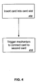
- FIG. 4 illustrates a method of coupling circuit cards together
- FIG. 5 illustrates a perspective view of a first tape library coupled to a second tape library using a circuit card such as that shown in FIGs. 1A and 1B.
- the circuit card 100 includes a first connector 132.
- the first connector 132 may be used to connect the card 100 to a first mating connector.
- the first mating connector may be a backplane of a storage device (e.g., tape library or disk device) or a server.
- the first connector may be any type of connector appropriate for making the connection to the first mating connector.
- the first connector may be an edge connector, a male connector, or a female connector. It should be appreciated that the type of connector may vary depending upon the configuration in which circuit card 100 is used.
- the circuit card 100 further includes a second connector 114.
- the second connector 114 is movable between first and second positions.
- FIG. 1A illustrates the second connector 114 in a first position
- FIG. 1B illustrates the second connector 114 in the second position.
- the second connector 114 may be used to connect the circuit card 100 to a second mating connector.
- the second mating connector may be a second circuit card coupled to a second storage device (e.g., tape library or disk device) or server.
- the second circuit card may be configured similarly or differently from circuit card 100.
- FIGs. 1A and 1B illustrate the second connector 114 moving down along a longitudal axis of the circuit card from the first position to the second position, other paths are also contemplated.
- second connector 114 may be moved upwards or along a latitudal axis of the circuit card to connect with second mating connector.
- Circuit card 100 additionally includes a mechanism 120 to move the second connector 114 between the first and second positions along a defined path.
- the mechanism 120 may be any type of mechanism that can cause the second connector 114 to move from a first position to a second position.
- the mechanism 120 may be triggered mechanically (e.g., a user moving the mechanism 120 from a first position to a second position) or electrically.
- the mechanism 120 may include a lever mechanism 122 pivotally connected to circuit card 100 with pivot 124.
- the second connector 114 may be moved between first and second positions by moving the lever mechanism 122 between a first and second position.
- moving the lever mechanism 122 downward from a first position to a second position may cause the second connector 114 to move downward and connect with second mating connector.
- Other configurations between mechanism 120, second connector 114, and circuit, card 100 are also contemptated.
- a button, switch, or sliding mechanism could be used to mechanically move or actuate the second connector 114 between the first and second positions.
- Mechanism 120 may further include a movable rigid material 116 coupled to second connector 114.
- Movable rigid material 116 may be a printed circuit board and may include circuitry that connects with circuitry on circuit card 100.
- Lever mechanism 120 is coupled to the rigid material with a pin 128 inserted into a channel 126 of the lever mechanism 120.
- movable rigid material 116 may be coupled between second connector 114 and circuitry on the circuit card 100 by a flexible connector 118 such as a ribbon cable. It should be appreciated that other configurations may also be used to connect second connector 114 with circuitry on the circuit card 100.
- second connector 114 may be directly connected to the circuit card with a flexible connector, such as a ribbon cable.
- circuit card 100 may be used to connect to a third mating connector.
- circuit card 100 may optionally include a third connector 130 to connect the circuit card 100 to a third mating connector.
- the third mating connector may be a third circuit card connected to a third storage device.
- the third storage device may be vertically stacked on a second storage device that is coupled to circuit card 100 via first connector 132.
- One or more additional storage devices may be stacked on top of third, storage device in a similar configuration as that between second and third storage devices.
- third connector 130 may share a common axis with second mating connector 114. Other configurations between second connector 114 and third connector 130 are also contemplated.
- circuit card 100 to connect two devices, only one card slot is required for the connection as the circuit card 100 may provide both a mechanical and electrical connection between the two devices. Additionally, by using mechanism 120 to move the second connector 114 along a defined path, the pins of the connectors may be less likely to become damaged than if a manual connection process is used to connect connector 114 to second mating connector.
- FIG. 2 illustrates an exemplary configuration in which circuit card 100 may be used.
- FIG. 2 illustrates a housing 200, such as a storage device housing.
- the housing 200 may include one or more slots 202-208 to receive circuit cards.
- a variety of different types of devices, such as storage devices (tape libraries, disk devices) or servers, may be inserted into storage device housing.
- the backplane 210 of a device inserted into storage device housing 200 may include a plurality of mating connectors 212-218 aligned with card slots 202-208.
- Housing 200 may further include card positioning rails 232, 234.
- Card positioning rails may be positioned on either or both the top and bottom of one or more card slots 202-208. The card positioning rails may be used to correctly align cards inserted into card slots 202-208 with the backplane connectors 212-218.
- housing 200 includes a slot 220 vertically aligned with a slot 230.
- Slot 230 may allow a movable connector 114 on a circuit card 100 to move downward to mate with a second circuit card inserted into a second housing stacked below housing 200.
- the second housing may be configured similar to housing 200 and a slot similar to slot 220 allows the second mating connector 114 to pass through the second storage device housing to mate with a connector on the second circuit card.
- slot 220 may be used to allow a movable connector from a third circuit card inserted into a third storage housing stacked above housing 200 to pass through storage device housing to mate with a connector 130 of a circuit card inserted into card slot 202.
- slots 220/230 may be horizontally aligned. Additionally, slots 220/230 may be positioned over any of the card slots 202-208.
- FIG. 3 illustrates: a device 350 (e.g., storage device or server) vertically stacked on a device 300.
- the devices 300, 350 may be connected by inserting a circuit card 360 into a slot of a housing holding storage device 350. Inserting circuit card 360 may cause a first connector 372 of the circuit card to connect with a mating connector on a backplane 380 of device 350.
- circuit card 310 is coupled to backplane 330 of device 300.
- circuit card 310 may be a control card, such as a library control card
- circuit card 360 may be a slave card.
- the mechanism triggered to connect circuit cards 310, 360 may include a lever mechanism that moves a movable connector 364 from a first position to a second position along a defined path, causing the movable connector 364 to mate with a mating connector on circuit card 310.
- the mechanism may further include a printed circuit board 366 that connects circuitry on the circuit card 310 to circuitry on circuit card 360 via ribbon cable 368.
- the devices 300, 350 may be disconnected by moving the lever mechanism from the second position back to the first position causing the movable connector 364 to become disconnected from circuit card 310.
- FIG. 5 illustrates an exemplary embodiment of two tape libraries 500, 550 coupled together.
- Tape library 500 includes tape drives 530, 532 and power supply 540.
- the housing of tape library 500 includes a plurality of card slots 502-508. Inserted into one of the slots is a circuit card 520, such as a library contcol card or a slave card. Circuit card 520 is connected to the backplane 510 of tape library 500.
- Tape library 550 includes tape drives 580, 582 and power supply 590.
- the housing of tape library 550 indudes a plurality of card slots 552-558. Inserted into one of the card slots 552 is a circuit card 100, such as that described with reference to FIGs. 1A and 1B.
- Circuit card 100 is coupled to a backplane 560 of tape library 550. As described elsewhere in this application, mechanism 120 has been triggered to cause circuit card 100 to become coupled to circuit card 520.
- circuit card 100 may act as a slave card to circuit card 520.
- Each tape library 500, 550 housing includes a slot to allow movable connector 114 to pass through the housing. Additionally, housing of tape library 500 includes a bottom slot 512 and housing of tape library 562 includes a top slot sharing a common axis with movable connector 114. These slots 512, 562 may allow additional libraries to be added to the configuration. It should be appreciated that alternate embodiments may not indude slots 512, 562.
Abstract
Description
- Modular storage devices, such as tape libraries, can be expanded by stacking devices together. One method that has been used to connect two storage devices is to include a circuit card in the second storage device to act as a slave to a control card of the base device. The devices are also connected with a cable that takes up one of the card slots on each of the devices. Thus, at least two card slots in the second device, one for the slave card and one for the cable, are used to connect the base device to the second storage device. Two card slots are also utilized in each additional device added to the configuration. Additionally, the pins on the connectors can become damaged during manual insertion of the cable connecting the devices together.
- In one embodiment, a circuit card with a movable connector is disclosed. The circuit card comprises a first connector to connect the circuit card to a first mating connector. Additionally, the circuit card includes a second connector that is movable between first and second positions. The second connector may be used to connect the circuit card to a second mating connector. The circuit card also includes a mechanism to move the second connector between the first and second positions along a defined path.
- Illustrative embodiments of the invention are illustrated in the drawings in which:
- FIG. 1A illustrates a first exemplary embodiment of a circuit card having a second connector in a first position;
- FIG. 1B illustrates the circuit card of FIG. 1A with the second connector in a second position;
- FIG. 2 illustrates a perspective of a storage device housing that may be used to hold the circuit card of FIGs 1A and 1B;
- FIG. 3 illustrates a side view of a first device coupled to a second device with a circuit card such as that shown in FIGs. 1A and 1B;
- FIG. 4 illustrates a method of coupling circuit cards together; and
- FIG. 5 illustrates a perspective view of a first tape library coupled to a second tape library using a circuit card such as that shown in FIGs. 1A and 1B.
- An exemplary circuit card with a movable connector is illustrated in FIGs. 1A and 1B. As shown in FIG. 1A, the
circuit card 100 includes afirst connector 132. Thefirst connector 132 may be used to connect thecard 100 to a first mating connector. In one embodiment, the first mating connector may be a backplane of a storage device (e.g., tape library or disk device) or a server. The first connector may be any type of connector appropriate for making the connection to the first mating connector. By way of example, the first connector may be an edge connector, a male connector, or a female connector. It should be appreciated that the type of connector may vary depending upon the configuration in whichcircuit card 100 is used. - The
circuit card 100 further includes asecond connector 114. Thesecond connector 114 is movable between first and second positions. FIG. 1A illustrates thesecond connector 114 in a first position, and FIG. 1B illustrates thesecond connector 114 in the second position. When in the second position, thesecond connector 114 may be used to connect thecircuit card 100 to a second mating connector. In one embodiment, the second mating connector may be a second circuit card coupled to a second storage device (e.g., tape library or disk device) or server. The second circuit card may be configured similarly or differently fromcircuit card 100. Although FIGs. 1A and 1B illustrate thesecond connector 114 moving down along a longitudal axis of the circuit card from the first position to the second position, other paths are also contemplated. For example,second connector 114 may be moved upwards or along a latitudal axis of the circuit card to connect with second mating connector. -
Circuit card 100 additionally includes amechanism 120 to move thesecond connector 114 between the first and second positions along a defined path. It should be appreciated that themechanism 120 may be any type of mechanism that can cause thesecond connector 114 to move from a first position to a second position. Themechanism 120 may be triggered mechanically (e.g., a user moving themechanism 120 from a first position to a second position) or electrically. - In one embodiment, the
mechanism 120 may include alever mechanism 122 pivotally connected tocircuit card 100 withpivot 124. Thesecond connector 114 may be moved between first and second positions by moving thelever mechanism 122 between a first and second position. By way of example, moving thelever mechanism 122 downward from a first position to a second position may cause thesecond connector 114 to move downward and connect with second mating connector. Other configurations betweenmechanism 120,second connector 114, and circuit,card 100 are also contemptated. For example, a button, switch, or sliding mechanism could be used to mechanically move or actuate thesecond connector 114 between the first and second positions. -
Mechanism 120 may further include a movablerigid material 116 coupled tosecond connector 114. Movablerigid material 116 may be a printed circuit board and may include circuitry that connects with circuitry oncircuit card 100.Lever mechanism 120 is coupled to the rigid material with apin 128 inserted into achannel 126 of thelever mechanism 120. In one embodiment, movablerigid material 116 may be coupled betweensecond connector 114 and circuitry on thecircuit card 100 by aflexible connector 118 such as a ribbon cable. It should be appreciated that other configurations may also be used to connectsecond connector 114 with circuitry on thecircuit card 100. By way of example,second connector 114 may be directly connected to the circuit card with a flexible connector, such as a ribbon cable. - In some embodiments,
circuit card 100 may be used to connect to a third mating connector. Thus,circuit card 100 may optionally include athird connector 130 to connect thecircuit card 100 to a third mating connector. In one embodiment, the third mating connector may be a third circuit card connected to a third storage device. The third storage device may be vertically stacked on a second storage device that is coupled tocircuit card 100 viafirst connector 132. One or more additional storage devices may be stacked on top of third, storage device in a similar configuration as that between second and third storage devices. To facilitate multiple device stacking,third connector 130 may share a common axis withsecond mating connector 114. Other configurations betweensecond connector 114 andthird connector 130 are also contemplated. - It should be appreciated that by using a
circuit card 100 to connect two devices, only one card slot is required for the connection as thecircuit card 100 may provide both a mechanical and electrical connection between the two devices. Additionally, by usingmechanism 120 to move thesecond connector 114 along a defined path, the pins of the connectors may be less likely to become damaged than if a manual connection process is used to connectconnector 114 to second mating connector. - FIG. 2 illustrates an exemplary configuration in which
circuit card 100 may be used. FIG. 2 illustrates ahousing 200, such as a storage device housing. Thehousing 200 may include one or more slots 202-208 to receive circuit cards. A variety of different types of devices, such as storage devices (tape libraries, disk devices) or servers, may be inserted into storage device housing. Thebackplane 210 of a device inserted intostorage device housing 200 may include a plurality of mating connectors 212-218 aligned with card slots 202-208. -
Housing 200 may further include card positioning rails 232, 234. Card positioning rails may be positioned on either or both the top and bottom of one or more card slots 202-208. The card positioning rails may be used to correctly align cards inserted into card slots 202-208 with the backplane connectors 212-218. - Additionally,
housing 200 includes aslot 220 vertically aligned with aslot 230.Slot 230 may allow amovable connector 114 on acircuit card 100 to move downward to mate with a second circuit card inserted into a second housing stacked belowhousing 200. In one embodiment, the second housing may be configured similar tohousing 200 and a slot similar to slot 220 allows thesecond mating connector 114 to pass through the second storage device housing to mate with a connector on the second circuit card. Similarly, slot 220 may be used to allow a movable connector from a third circuit card inserted into a third storage housing stacked abovehousing 200 to pass through storage device housing to mate with aconnector 130 of a circuit card inserted intocard slot 202. - It should be appreciated that configurations other than that depicted in FIG. 2 are also contemplated. By way of example,
slots 220/230 may be horizontally aligned. Additionally,slots 220/230 may be positioned over any of the card slots 202-208. - FIG. 3 illustrates: a device 350 (e.g., storage device or server) vertically stacked on a
device 300. As illustrated by FIG. 4, thedevices circuit card 360 into a slot of a housing holdingstorage device 350. Insertingcircuit card 360 may cause afirst connector 372 of the circuit card to connect with a mating connector on abackplane 380 ofdevice 350. - Next, a
mechanism 362 is triggered 410 to connectcircuit card 360 tocircuit card 310.Circuit card 310 is coupled tobackplane 330 ofdevice 300. By way of example,circuit card 310 may be a control card, such as a library control card, andcircuit card 360 may be a slave card. In one embodiment, the mechanism triggered to connectcircuit cards movable connector 364 from a first position to a second position along a defined path, causing themovable connector 364 to mate with a mating connector oncircuit card 310. The mechanism may further include a printedcircuit board 366 that connects circuitry on thecircuit card 310 to circuitry oncircuit card 360 viaribbon cable 368. Thedevices movable connector 364 to become disconnected fromcircuit card 310. - FIG. 5 illustrates an exemplary embodiment of two
tape libraries Tape library 500 includes tape drives 530, 532 andpower supply 540. The housing oftape library 500 includes a plurality of card slots 502-508. Inserted into one of the slots is acircuit card 520, such as a library contcol card or a slave card.Circuit card 520 is connected to thebackplane 510 oftape library 500. -
Tape library 550 includes tape drives 580, 582 andpower supply 590. The housing oftape library 550 indudes a plurality of card slots 552-558. Inserted into one of thecard slots 552 is acircuit card 100, such as that described with reference to FIGs. 1A and1B. Circuit card 100 is coupled to abackplane 560 oftape library 550. As described elsewhere in this application,mechanism 120 has been triggered to causecircuit card 100 to become coupled tocircuit card 520. In one embodiment,circuit card 100 may act as a slave card tocircuit card 520. - Each
tape library movable connector 114 to pass through the housing. Additionally, housing oftape library 500 includes abottom slot 512 and housing oftape library 562 includes a top slot sharing a common axis withmovable connector 114. Theseslots indude slots
Claims (10)
- A circuit card (100) comprising:a first connector (132) to connect the circuit card to a first mating connector;a second connector (114), movable between first and second positions, to connect the circuit card to a second mating connector; anda mechanism (120) to move the second connector between the first and second positions along a defined path.
- The circuit card of claim 1, wherein the first mating connector comprises a backplane (380) of a first storage device (350).
- The circuit card of claim 2, wherein the second mating connector comprises a second circuit card (310), the second circuit card coupled to a second storage device (300).
- The circuit card of claim 3, further comprising a third connector (130) sharing a common axis with the second position of the second connector, the third connector to connect the circuit card to a third circuit card coupled to a third storage device.
- The circuit card of any of claims 1-4, wherein the mechanism includes a lever mechanism (122) pivotally coupled to the circuit card.
- A method comprising:inserting (400) a first circuit card into a card slot of a first housing; andconnecting the first circuit card to a second circuit card in a second housing by triggering (410) a mechanism on the first circuit card.
- The method of claim 6, wherein inserting a first circuit card comprises connecting the first circuit card to a backplane of a first storage device in the first housing.
- The method of claims 6 or 7, wherein the first circuit card comprises a movable connector and triggering a mechanism comprises causing the movable connector to move from a first position to a second position.
- A system comprising:a first storage device housing (200) including a first card slot (202);a first storage device (300) inserted into the first storage device housing;a first circuit card (310) inserted into the first card slot, the first circuit card connected to a backplane (330) of the first storage device;a second storage device housing vertically stacked on the first storage device housing, the second storage device housing including a second card slot;a second storage device (350) inserted into the second storage device housing; anda second circuit card (360) inserted into the second card slot, the second circuit card including:a first connector (372) to connect the circuit card to a backplane (380) of the second storage device;a second connector (364), movable between first and second positions, when in the second position to connect the second circuit card to the first circuit card; anda mechanism (120) to move the second connector between the first and second positions.
- The system of claim 9, wherein the mechanism includes a lever mechanism (362) pivotally coupled to the circuit card and a printed circuit board (366) coupled to the second connector and the lever mechanism.
Applications Claiming Priority (2)
| Application Number | Priority Date | Filing Date | Title |
|---|---|---|---|
| US678867 | 2003-10-03 | ||
| US10/678,867 US6926548B2 (en) | 2003-10-03 | 2003-10-03 | Circuit card |
Publications (3)
| Publication Number | Publication Date |
|---|---|
| EP1521512A2 true EP1521512A2 (en) | 2005-04-06 |
| EP1521512A3 EP1521512A3 (en) | 2006-09-13 |
| EP1521512B1 EP1521512B1 (en) | 2008-07-30 |
Family
ID=34314081
Family Applications (1)
| Application Number | Title | Priority Date | Filing Date |
|---|---|---|---|
| EP04255880A Expired - Fee Related EP1521512B1 (en) | 2003-10-03 | 2004-09-27 | Circuit card |
Country Status (4)
| Country | Link |
|---|---|
| US (1) | US6926548B2 (en) |
| EP (1) | EP1521512B1 (en) |
| JP (1) | JP3950131B2 (en) |
| DE (1) | DE602004015387D1 (en) |
Cited By (1)
| Publication number | Priority date | Publication date | Assignee | Title |
|---|---|---|---|---|
| ITRN20100046A1 (en) * | 2010-08-05 | 2012-02-06 | Indesit Co Spa | APPLIANCE |
Families Citing this family (10)
| Publication number | Priority date | Publication date | Assignee | Title |
|---|---|---|---|---|
| US7378836B2 (en) | 2006-01-10 | 2008-05-27 | Spansion, Llc | Automated loading/unloading of devices for burn-in testing |
| US7291032B1 (en) * | 2006-07-05 | 2007-11-06 | International Business Machines Corporation | Connector for adjacent devices |
| US7654844B1 (en) * | 2008-08-22 | 2010-02-02 | International Business Machines Corporation | Telescopic power connector |
| IT1390947B1 (en) * | 2008-08-27 | 2011-10-27 | Esaote Spa | MULTIPOLAR CONNECTION DEVICE |
| CN102043442B (en) * | 2009-10-26 | 2014-04-23 | 鸿富锦精密工业(深圳)有限公司 | Server system and serve cabinet |
| JP5614250B2 (en) * | 2010-11-09 | 2014-10-29 | 富士通株式会社 | Electrical connection device between electronic devices |
| US20130189863A1 (en) * | 2012-01-19 | 2013-07-25 | International Business Machines Corporation | Connector system |
| US9383786B2 (en) * | 2012-12-14 | 2016-07-05 | Dell Products L.P. | Telescoping enclosure for information handling system component |
| US9360899B2 (en) | 2014-02-03 | 2016-06-07 | Adtran, Inc. | Communication module having a rotatable connector assembly for multiple connection orientations |
| CN111613956B (en) * | 2019-02-26 | 2024-02-06 | 纬联电子科技(中山)有限公司 | Plug assembly |
Citations (4)
| Publication number | Priority date | Publication date | Assignee | Title |
|---|---|---|---|---|
| EP0104982A1 (en) * | 1982-09-17 | 1984-04-04 | Thomson-Brandt | Read-write apparatus and computer, especially a microcumputer, comprising such an apparatus |
| EP1076283A2 (en) * | 1999-08-12 | 2001-02-14 | Hewlett-Packard Company | System for enabling stacking of autochanger modules |
| US6275385B1 (en) * | 1998-12-18 | 2001-08-14 | Denso Corporation | Electronic control device and jig device therefor having casing inclination compensating part |
| EP1275993A1 (en) * | 2001-07-11 | 2003-01-15 | Lucent Technologies Inc. | Optical fibre connector mechanism |
Family Cites Families (3)
| Publication number | Priority date | Publication date | Assignee | Title |
|---|---|---|---|---|
| US6640235B1 (en) * | 1992-08-20 | 2003-10-28 | Intel Corporation | Expandable mass disk drive storage system |
| US6148352A (en) * | 1997-12-24 | 2000-11-14 | International Business Machines Corporation | Scalable modular data storage system |
| US6272573B1 (en) * | 1997-12-24 | 2001-08-07 | International Business Machines Corporation | Scalable modular data storage system |
-
2003
- 2003-10-03 US US10/678,867 patent/US6926548B2/en not_active Expired - Fee Related
-
2004
- 2004-09-22 JP JP2004274608A patent/JP3950131B2/en not_active Expired - Fee Related
- 2004-09-27 DE DE602004015387T patent/DE602004015387D1/en active Active
- 2004-09-27 EP EP04255880A patent/EP1521512B1/en not_active Expired - Fee Related
Patent Citations (4)
| Publication number | Priority date | Publication date | Assignee | Title |
|---|---|---|---|---|
| EP0104982A1 (en) * | 1982-09-17 | 1984-04-04 | Thomson-Brandt | Read-write apparatus and computer, especially a microcumputer, comprising such an apparatus |
| US6275385B1 (en) * | 1998-12-18 | 2001-08-14 | Denso Corporation | Electronic control device and jig device therefor having casing inclination compensating part |
| EP1076283A2 (en) * | 1999-08-12 | 2001-02-14 | Hewlett-Packard Company | System for enabling stacking of autochanger modules |
| EP1275993A1 (en) * | 2001-07-11 | 2003-01-15 | Lucent Technologies Inc. | Optical fibre connector mechanism |
Cited By (2)
| Publication number | Priority date | Publication date | Assignee | Title |
|---|---|---|---|---|
| ITRN20100046A1 (en) * | 2010-08-05 | 2012-02-06 | Indesit Co Spa | APPLIANCE |
| EP2416631A1 (en) * | 2010-08-05 | 2012-02-08 | Indesit Company S.p.A. | Electrical household appliance comprising means for displaying an item of information |
Also Published As
| Publication number | Publication date |
|---|---|
| US6926548B2 (en) | 2005-08-09 |
| EP1521512A3 (en) | 2006-09-13 |
| US20050074994A1 (en) | 2005-04-07 |
| EP1521512B1 (en) | 2008-07-30 |
| JP2005115935A (en) | 2005-04-28 |
| JP3950131B2 (en) | 2007-07-25 |
| DE602004015387D1 (en) | 2008-09-11 |
Similar Documents
| Publication | Publication Date | Title |
|---|---|---|
| JP3527812B2 (en) | IC card connector | |
| US4445740A (en) | Circuit board assembly | |
| US6935873B2 (en) | Electrical connector | |
| KR0151755B1 (en) | Connector apparatus for ic packs | |
| US5330363A (en) | IC pack connector apparatus with switch means | |
| US5299089A (en) | Connector device having two storage decks and three contact arrays for one hard disk drive package or two memory cards | |
| US7445494B2 (en) | Electrical connector with retaining member | |
| TWI544695B (en) | Connector assemblies and daughter card assemblies configured to engage each other along a side interface | |
| WO1980001022A1 (en) | Connector device for printed circuit boards | |
| US8113851B2 (en) | Connector assemblies and systems including flexible circuits | |
| US6926548B2 (en) | Circuit card | |
| JPS6014776A (en) | Zero inserting input connector | |
| US20060105621A1 (en) | Connector for flexible printed circuit | |
| US8282290B2 (en) | Connectors and assemblies having a plurality of moveable mating arrays | |
| US5860828A (en) | PCMCIA card connector that minimizes bent contact pins | |
| US6663440B2 (en) | Printed circuit board for pin array connection | |
| US6174186B1 (en) | Card connector | |
| US8215964B2 (en) | Connectors and assemblies having a plurality of moveable mating arrays | |
| US6776664B1 (en) | Electrical connector with retention and guiding means | |
| US6921278B2 (en) | Method and apparatus for electrically connecting two objects | |
| US4594490A (en) | Terminal pin shorting switch apparatus | |
| US6533597B1 (en) | Electrical connector having improved housing structure | |
| US7048560B2 (en) | System and method for ejecting a high extraction force electromechanical connector | |
| US5513079A (en) | Mass termination of signals from electronic systems to devices under test | |
| US20020137379A1 (en) | Electrical connector having associated card-ejecting means |
Legal Events
| Date | Code | Title | Description |
|---|---|---|---|
| PUAI | Public reference made under article 153(3) epc to a published international application that has entered the european phase |
Free format text: ORIGINAL CODE: 0009012 |
|
| AK | Designated contracting states |
Kind code of ref document: A2 Designated state(s): AT BE BG CH CY CZ DE DK EE ES FI FR GB GR HU IE IT LI LU MC NL PL PT RO SE SI SK TR |
|
| AX | Request for extension of the european patent |
Extension state: AL HR LT LV MK |
|
| RIN1 | Information on inventor provided before grant (corrected) |
Inventor name: REASONER, KELLY J. Inventor name: JONES, DAVID P. Inventor name: EHRLICH, RONALD L. |
|
| PUAL | Search report despatched |
Free format text: ORIGINAL CODE: 0009013 |
|
| AK | Designated contracting states |
Kind code of ref document: A3 Designated state(s): AT BE BG CH CY CZ DE DK EE ES FI FR GB GR HU IE IT LI LU MC NL PL PT RO SE SI SK TR |
|
| AX | Request for extension of the european patent |
Extension state: AL HR LT LV MK |
|
| 17P | Request for examination filed |
Effective date: 20070223 |
|
| AKX | Designation fees paid |
Designated state(s): DE FR GB |
|
| 17Q | First examination report despatched |
Effective date: 20070705 |
|
| GRAP | Despatch of communication of intention to grant a patent |
Free format text: ORIGINAL CODE: EPIDOSNIGR1 |
|
| GRAS | Grant fee paid |
Free format text: ORIGINAL CODE: EPIDOSNIGR3 |
|
| GRAA | (expected) grant |
Free format text: ORIGINAL CODE: 0009210 |
|
| AK | Designated contracting states |
Kind code of ref document: B1 Designated state(s): DE FR GB |
|
| REG | Reference to a national code |
Ref country code: GB Ref legal event code: FG4D |
|
| REF | Corresponds to: |
Ref document number: 602004015387 Country of ref document: DE Date of ref document: 20080911 Kind code of ref document: P |
|
| PLBE | No opposition filed within time limit |
Free format text: ORIGINAL CODE: 0009261 |
|
| STAA | Information on the status of an ep patent application or granted ep patent |
Free format text: STATUS: NO OPPOSITION FILED WITHIN TIME LIMIT |
|
| REG | Reference to a national code |
Ref country code: FR Ref legal event code: ST Effective date: 20090529 |
|
| 26N | No opposition filed |
Effective date: 20090506 |
|
| PG25 | Lapsed in a contracting state [announced via postgrant information from national office to epo] |
Ref country code: FR Free format text: LAPSE BECAUSE OF NON-PAYMENT OF DUE FEES Effective date: 20080930 |
|
| PGFP | Annual fee paid to national office [announced via postgrant information from national office to epo] |
Ref country code: DE Payment date: 20130820 Year of fee payment: 10 |
|
| PGFP | Annual fee paid to national office [announced via postgrant information from national office to epo] |
Ref country code: GB Payment date: 20130823 Year of fee payment: 10 |
|
| REG | Reference to a national code |
Ref country code: DE Ref legal event code: R119 Ref document number: 602004015387 Country of ref document: DE |
|
| GBPC | Gb: european patent ceased through non-payment of renewal fee |
Effective date: 20140927 |
|
| REG | Reference to a national code |
Ref country code: DE Ref legal event code: R119 Ref document number: 602004015387 Country of ref document: DE Effective date: 20150401 |
|
| PG25 | Lapsed in a contracting state [announced via postgrant information from national office to epo] |
Ref country code: DE Free format text: LAPSE BECAUSE OF NON-PAYMENT OF DUE FEES Effective date: 20150401 Ref country code: GB Free format text: LAPSE BECAUSE OF NON-PAYMENT OF DUE FEES Effective date: 20140927 |