EP1533848A2 - Electroluminescence display - Google Patents
Electroluminescence display Download PDFInfo
- Publication number
- EP1533848A2 EP1533848A2 EP04090447A EP04090447A EP1533848A2 EP 1533848 A2 EP1533848 A2 EP 1533848A2 EP 04090447 A EP04090447 A EP 04090447A EP 04090447 A EP04090447 A EP 04090447A EP 1533848 A2 EP1533848 A2 EP 1533848A2
- Authority
- EP
- European Patent Office
- Prior art keywords
- power supply
- supply voltage
- line
- electro luminescence
- luminescence display
- Prior art date
- Legal status (The legal status is an assumption and is not a legal conclusion. Google has not performed a legal analysis and makes no representation as to the accuracy of the status listed.)
- Granted
Links
- 238000005401 electroluminescence Methods 0.000 title claims abstract description 43
- DTTPWCNKTMQMTE-TYNNPWLESA-N [(1R,2S,3S,4S,5R,6S,8R,12S,13S,16R,19S,20R,21S)-14-ethyl-2-hydroxy-4,6,19-trimethoxy-16-methyl-9,11-dioxa-14-azaheptacyclo[10.7.2.12,5.01,13.03,8.08,12.016,20]docosan-21-yl] acetate Chemical group CCN1C[C@]2(C)CC[C@H](OC)[C@]34[C@@H]2[C@H](OC(C)=O)[C@@]2(OCO[C@@]22C[C@H](OC)[C@H]5C[C@]3(O)[C@@H]2[C@H]5OC)[C@@H]14 DTTPWCNKTMQMTE-TYNNPWLESA-N 0.000 claims abstract description 7
- 230000005684 electric field Effects 0.000 claims abstract description 3
- 239000002184 metal Substances 0.000 claims description 32
- 239000011159 matrix material Substances 0.000 description 5
- 239000000969 carrier Substances 0.000 description 1
- 239000004973 liquid crystal related substance Substances 0.000 description 1
- 239000000463 material Substances 0.000 description 1
- 238000012986 modification Methods 0.000 description 1
- 230000004048 modification Effects 0.000 description 1
- 238000011160 research Methods 0.000 description 1
Images


Classifications
-
- H—ELECTRICITY
- H10—SEMICONDUCTOR DEVICES; ELECTRIC SOLID-STATE DEVICES NOT OTHERWISE PROVIDED FOR
- H10K—ORGANIC ELECTRIC SOLID-STATE DEVICES
- H10K59/00—Integrated devices, or assemblies of multiple devices, comprising at least one organic light-emitting element covered by group H10K50/00
- H10K59/10—OLED displays
- H10K59/12—Active-matrix OLED [AMOLED] displays
- H10K59/131—Interconnections, e.g. wiring lines or terminals
-
- G—PHYSICS
- G09—EDUCATION; CRYPTOGRAPHY; DISPLAY; ADVERTISING; SEALS
- G09G—ARRANGEMENTS OR CIRCUITS FOR CONTROL OF INDICATING DEVICES USING STATIC MEANS TO PRESENT VARIABLE INFORMATION
- G09G3/00—Control arrangements or circuits, of interest only in connection with visual indicators other than cathode-ray tubes
- G09G3/20—Control arrangements or circuits, of interest only in connection with visual indicators other than cathode-ray tubes for presentation of an assembly of a number of characters, e.g. a page, by composing the assembly by combination of individual elements arranged in a matrix no fixed position being assigned to or needed to be assigned to the individual characters or partial characters
-
- H—ELECTRICITY
- H01—ELECTRIC ELEMENTS
- H01L—SEMICONDUCTOR DEVICES NOT COVERED BY CLASS H10
- H01L27/00—Devices consisting of a plurality of semiconductor or other solid-state components formed in or on a common substrate
- H01L27/02—Devices consisting of a plurality of semiconductor or other solid-state components formed in or on a common substrate including semiconductor components specially adapted for rectifying, oscillating, amplifying or switching and having at least one potential-jump barrier or surface barrier; including integrated passive circuit elements with at least one potential-jump barrier or surface barrier
- H01L27/0203—Particular design considerations for integrated circuits
- H01L27/0207—Geometrical layout of the components, e.g. computer aided design; custom LSI, semi-custom LSI, standard cell technique
Definitions
- the present invention relates to an electro luminescence display and, more particularly, to an electro luminescence display in which an electromagnetic interference (EMI) shielding means capable of shielding the EMI by having a shielding means in a first power supply voltage line is contained to prevent noise or the like of the power supply voltage due to an internal or external EMI from occurring.
- EMI electromagnetic interference
- Such a flat panel display includes a liquid crystal display, a field emission display, a plasma display panel, an electro luminescence display, and the like.
- the electro luminescence display uses carriers such as electrons and holes to excite a fluorescent material to display image or video so that it may be driven by a low direct voltage and has a faster response speed.
- the electro luminescence display has been in the spotlight as the next generation display and researches on new products have accelerated in recent years.
- This electro luminescence display may be mainly classified into a passive matrix type and an active matrix type, and the active matrix electro luminescence display has an active switching device arranged in each pixel and has a voltage or current in response to the image data of the pixel applied to drive each emitting device.
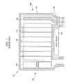
- Such an active matrix type electro luminescence display is shown in FIG. 1.
- FIG. 1 is a plan view of a conventional active matrix type electro luminescence display.
- Numerical reference 100 indicates an electro luminescence display
- 110 indicates a first upper power supply voltage line
- 120 indicates a first lower power supply voltage line
- 130 indicates a second power supply voltage line
- 140 indicates a scan driver
- 150 indicates a data driver
- 160 indicates a first active power supply voltage line
- 170 indicates a pixel region.
- the conventional electro luminescence display 100 includes the scan driver 140 applying a selection signal, the data driver 150 applying a data signal, the pixel region 170 emitting light in response to the selection signal and the data signal applied from the scan driver 140 and the data driver 150, the first upper and lower power supply voltage lines 110 and 120 delivering first power supply voltages, the second power supply line 130 delivering a second power supply voltage, and the first active power supply voltage line 160 applying, the power supply voltages delivered from the first power supply voltage lines 110 and 120 and the second power supply voltage delivered to the second power supply voltage line 130, to the pixel region 170.
- each of the first power supply voltages is opposite to that of the second power supply voltage.
- the conventional electro luminescence display as described above has a problem that the waveform of the power supply voltage is distorted due to an internally or externally applied electromagnetic wave. That is, the power supply voltages delivered through the first upper and lower power supply voltage lines have noises which are resulted from the electromagnetic wave externally or internally delivered to thereby have non-uniformity in brightness.
- the present invention therefore, solves aforementioned problems associated with conventional devices by providing an electro luminescence display having an EMI shielding means parallel to first power supply voltage lines wherein a specific voltage is applied to the EMI shielding means to pull the electromagnetic wave so that the electromagnetic wave otherwise affecting the power supply voltage may be shielded.
- an electro luminescence display including: a pixel region in which devices are arranged in a stripe line structure or in a delta line structure to emit light in response to a data signal; a scan driver applying a switching signal to a gate electrode of a first switching device; a data driver applying data information to a source electrode of the first switching device; and a power supply line having a conductive characteristic of applying a first power supply voltage to the pixel region
- the electro luminescence display includes a means for shielding an electromagnetic wave having electronic field or magnetic field characteristics.
- the electro luminescence display may further include a shielding voltage generating means for applying a voltage to the means for shielding the electronic field or magnetic field.
- the means for shielding the electronic field or magnetic field may generate a second power supply voltage.
- the second power supply voltage may have a polarity opposite to that of the first power supply voltage.
- the means for shielding the electronic field or magnetic field may be a conductive interconnection line arranged parallel to the first power supply voltage line.
- an electro luminescence display including: a pixel region in which devices are arranged in a stripe line structure or in a delta line structure to emit light in response to a data signal; a scan driver applying a switching signal to a gate electrode of a first switching device; a data driver applying data information to a source electrode of the first switching device; and a power supply line having a conductive characteristic of applying a first power supply voltage to the pixel region, the electro luminescence display includes a metal line arranged parallel to the first power supply voltage line.
- the metal line may be arranged inside the first power supply voltage line.
- the metal line may be arranged outside the first power supply voltage line.
- the metal lines may be arranged inside and outside the power supply voltage line, respectively.
- the electro luminescence display may further include a shielding voltage generating means for applying a voltage to the metal line.
- the shielding voltage generating means may apply a second power supply voltage having a polarity opposite to that of the first power supply voltage to the metal line.
- an electro luminescence display including: a pixel region in which devices are arranged in a row or in a delta line structure to emit light in response to a data signal; a scan driver applying a switching signal to a gate electrode of a first switching device; a data driver applying data information to a source electrode of the first switching device; and a power supply line having a conductive characteristic of applying a first power supply voltage to the pixel region, the electro luminescence display includes a metal line arranged parallel to the first power supply voltage line to be connected to a ground terminal.
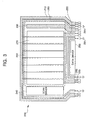
- FIG. 2 is a plan view of a first embodiment of the present invention.
- Numerical reference 200 indicates an electro luminescence display
- 210 indicates a first upper power supply line
- 220 indicates a first lower power supply voltage line
- 230 indicates a second power supply voltage line
- 240 indicates a scan driver
- 250 indicates a data driver
- 260 indicates a first active power supply voltage line
- 270 indicates a pixel region
- 280 indicates a metal line
- 290 indicates a shielding voltage generation means.
- the electro luminescence display 200 includes the scan driver 240, the data driver 250, the pixel region 270 emitting light in response to a selection signal and a data signal applied from the scan driver 240 and the data driver 250, the first upper and lower power supply voltage lines 210 and 220 delivering first power supply voltages, the first active power supply voltage line 260 applying the power supply voltages delivered from the first power supply voltage lines 210 and 220 to the pixel region 270, the second power supply voltage line 230 applying a second power supply voltage to the pixel region 270, the metal line 280 arranged parallel to the first power supply voltage lines 210 and 220 to shield an electromagnetic wave, and the shielding voltage generation means 290 for applying a shielding voltage to the metal line 280.
- switching and drive transistors (not shown) of the pixel region 270 are turned on.
- the drive transistor of the pixel region 270 is turned on, the power supply voltages applied to the first upper and lower power supply voltage lines 210 and 220 are applied to the pixel region 270 through the first active power supply voltage line 260, so that the pixel region 270 emits light.
- the shielding voltage generation means 290 applies a specific voltage to the metal line 280 so that the specific current flows through the metal line 280 arranged parallel to each of the first upper and lower power supply voltage lines 210 and 220.
- the specific voltage applied to the metal line 280 preferably has a polarity opposite to that of each first power supply voltage.
- the metal line 280 and the first power supply voltage line 210 are spaced apart from each other by a constant interval to be parallel to each other as shown in FIGs. 2 and 3, however, the metal line 280 and the first power supply voltage line 210 may be isolated from each other by a separate insulating means interposed therebetween to achieve the purpose of the present invention in cases.
- the electromagnetic wave having magnetic field or electric field characteristics applied from an external source is applied to the first power supply voltage lines 210 and 220
- the electromagnetic wave is shielded by the metal line 280 arranged parallel to the first power supply voltage lines 210 and 220. That is, the voltage applied to the metal line 280 has a polarity opposite to that of the first power supply voltage so that the electromagnetic wave is pulled by the metal line 280 by means of electrical characteristics which flow from positive to negative or from negative to positive.
- the power supply voltage is not affected by the electromagnetic wave.
- FIG. 3 is a plan view of a second embodiment of the present invention.
- another embodiment of the present invention has ground terminals 291 each connected to the metal line 280. Accordingly, the electromagnetic wave applied to the first power supply voltage lines 210 and 220 is pulled by the metal line 280 to be grounded so that the power supply voltages are shielded from the electromagnetic wave.
- FIG. 4 is a plan view of a third embodiment of the present invention.
- the metal line 280 is arranged in the first upper power supply voltage line 210 in the first embodiment, however, it may be arranged outside the first upper power supply voltage line 210 in the third embodiment, which also describes the main point of the present invention.
- the metal line 280 is arranged outside the first upper power supply voltage line 210 so as to be spaced apart or insulated from the first upper power supply voltage line 210 by a constant interval or by an insulating means (not shown) respectively, so that the electromagnetic wave applied from an external source may be shielded.
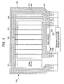
- FIG. 5 is a plan view of a fourth embodiment of the present invention.
- the metal lines 280 are arranged inside and outside the first upper power supply voltage line 210 to shield the electromagnetic wave applied from an external source. That is, a specific voltage is applied to the metal lines 280 arranged inside and outside the first upper power supply voltage line 210 so that the electromagnetic wave applied from the external source may be shielded.
- the electromagnetic wave may be shielded by the metal line arranged parallel to the first power supply voltage lines so that noises of the power supply voltage do not occur, which allows non-uniformity in brightness due to the electromagnetic wave to be improved.
Abstract
Description
- This application claims priority to and the benefit of Korean Patent Application No. 2003-82391, filed November 19, 2003, the disclosure of which is incorporated herein by reference in its entirety.
- The present invention relates to an electro luminescence display and, more particularly, to an electro luminescence display in which an electromagnetic interference (EMI) shielding means capable of shielding the EMI by having a shielding means in a first power supply voltage line is contained to prevent noise or the like of the power supply voltage due to an internal or external EMI from occurring.
- In recent years, various flat panel displays are developed which are capable of reducing weight and volume which are disadvantages of a cathode ray tube (CRT). Such a flat panel display includes a liquid crystal display, a field emission display, a plasma display panel, an electro luminescence display, and the like.
- Among these displays, the electro luminescence display uses carriers such as electrons and holes to excite a fluorescent material to display image or video so that it may be driven by a low direct voltage and has a faster response speed. By these reasons, the electro luminescence display has been in the spotlight as the next generation display and researches on new products have accelerated in recent years.
- This electro luminescence display may be mainly classified into a passive matrix type and an active matrix type, and the active matrix electro luminescence display has an active switching device arranged in each pixel and has a voltage or current in response to the image data of the pixel applied to drive each emitting device. Such an active matrix type electro luminescence display is shown in FIG. 1.
- FIG. 1 is a plan view of a conventional active matrix type electro luminescence display.
-
Numerical reference 100 indicates an electro luminescence display, 110 indicates a first upper power supply voltage line, 120 indicates a first lower power supply voltage line, 130 indicates a second power supply voltage line, 140 indicates a scan driver, 150 indicates a data driver, 160 indicates a first active power supply voltage line, and 170 indicates a pixel region. - As shown in the FIG. 1, the conventional
electro luminescence display 100 includes thescan driver 140 applying a selection signal, thedata driver 150 applying a data signal, thepixel region 170 emitting light in response to the selection signal and the data signal applied from thescan driver 140 and thedata driver 150, the first upper and lower powersupply voltage lines power supply line 130 delivering a second power supply voltage, and the first active powersupply voltage line 160 applying, the power supply voltages delivered from the first powersupply voltage lines supply voltage line 130, to thepixel region 170. - When the selection signal and the data signal are applied from the
scan driver 140 and thedata driver 150 to thepixel region 170, switching transistors drive transistors (not shown) of thepixel region 170 are driven, and the first and second power supply voltages are applied to thepixel region 170 through the first powersupply voltage lines supply voltage line 130 so that each pixel of thepixel region 170 emits light. In this case, each of the first power supply voltages is opposite to that of the second power supply voltage. - However, the conventional electro luminescence display as described above has a problem that the waveform of the power supply voltage is distorted due to an internally or externally applied electromagnetic wave. That is, the power supply voltages delivered through the first upper and lower power supply voltage lines have noises which are resulted from the electromagnetic wave externally or internally delivered to thereby have non-uniformity in brightness.
- The present invention, therefore, solves aforementioned problems associated with conventional devices by providing an electro luminescence display having an EMI shielding means parallel to first power supply voltage lines wherein a specific voltage is applied to the EMI shielding means to pull the electromagnetic wave so that the electromagnetic wave otherwise affecting the power supply voltage may be shielded.
- In an exemplary embodiment of the present invention, an electro luminescence display including: a pixel region in which devices are arranged in a stripe line structure or in a delta line structure to emit light in response to a data signal; a scan driver applying a switching signal to a gate electrode of a first switching device; a data driver applying data information to a source electrode of the first switching device; and a power supply line having a conductive characteristic of applying a first power supply voltage to the pixel region, the electro luminescence display includes a means for shielding an electromagnetic wave having electronic field or magnetic field characteristics.
- The electro luminescence display may further include a shielding voltage generating means for applying a voltage to the means for shielding the electronic field or magnetic field.
- The means for shielding the electronic field or magnetic field may generate a second power supply voltage.
- Moreover, the second power supply voltage may have a polarity opposite to that of the first power supply voltage.
- The means for shielding the electronic field or magnetic field may be a conductive interconnection line arranged parallel to the first power supply voltage line.
- In another exemplary embodiment according to the present invention, an electro luminescence display including: a pixel region in which devices are arranged in a stripe line structure or in a delta line structure to emit light in response to a data signal; a scan driver applying a switching signal to a gate electrode of a first switching device; a data driver applying data information to a source electrode of the first switching device; and a power supply line having a conductive characteristic of applying a first power supply voltage to the pixel region, the electro luminescence display includes a metal line arranged parallel to the first power supply voltage line.
- Moreover, the metal line may be arranged inside the first power supply voltage line.
- Alternatively, the metal line may be arranged outside the first power supply voltage line.
- Alternatively, the metal lines may be arranged inside and outside the power supply voltage line, respectively.
- In addition, the electro luminescence display may further include a shielding voltage generating means for applying a voltage to the metal line.
- In addition, the shielding voltage generating means may apply a second power supply voltage having a polarity opposite to that of the first power supply voltage to the metal line.
- In yet another exemplary embodiment according to the present invention, an electro luminescence display including: a pixel region in which devices are arranged in a row or in a delta line structure to emit light in response to a data signal; a scan driver applying a switching signal to a gate electrode of a first switching device; a data driver applying data information to a source electrode of the first switching device; and a power supply line having a conductive characteristic of applying a first power supply voltage to the pixel region, the electro luminescence display includes a metal line arranged parallel to the first power supply voltage line to be connected to a ground terminal.
- The above and other features of the present invention will be described in reference to certain exemplary embodiments thereof with reference to the attached drawings in which:
- FIG. 1 is a plan view of a conventional electro luminescence display of the conventional art;
- FIG. 2 is a plan view of a first embodiment of the present invention;
- FIG. 3 is a plan view of a second embodiment of the present invention;
- FIG. 4 is a plan view of a third embodiment of the present invention; and
- FIG. 5 is a plan view of a fourth embodiment of the present invention.
-
- The present invention will now be described more fully hereinafter with reference to the accompanying drawings, in which preferred embodiments of the invention are shown.
- FIG. 2 is a plan view of a first embodiment of the present invention.
-
Numerical reference 200 indicates an electro luminescence display, 210 indicates a first upper power supply line, 220 indicates a first lower power supply voltage line, 230 indicates a second power supply voltage line, 240 indicates a scan driver, 250 indicates a data driver, 260 indicates a first active power supply voltage line, 270 indicates a pixel region, 280 indicates a metal line, and 290 indicates a shielding voltage generation means. - As shown in FIG. 2, the
electro luminescence display 200 according to the present invention includes thescan driver 240, thedata driver 250, thepixel region 270 emitting light in response to a selection signal and a data signal applied from thescan driver 240 and thedata driver 250, the first upper and lower powersupply voltage lines supply voltage line 260 applying the power supply voltages delivered from the first powersupply voltage lines pixel region 270, the second powersupply voltage line 230 applying a second power supply voltage to thepixel region 270, themetal line 280 arranged parallel to the first powersupply voltage lines metal line 280. - When the selection signal and the data signal are applied from the
scan driver 240 and thedata driver 250 to thepixel region 270, switching and drive transistors (not shown) of thepixel region 270 are turned on. As the drive transistor of thepixel region 270 is turned on, the power supply voltages applied to the first upper and lower powersupply voltage lines pixel region 270 through the first active powersupply voltage line 260, so that thepixel region 270 emits light. - In addition, the shielding voltage generation means 290 applies a specific voltage to the
metal line 280 so that the specific current flows through themetal line 280 arranged parallel to each of the first upper and lower powersupply voltage lines metal line 280 preferably has a polarity opposite to that of each first power supply voltage. - In addition, the
metal line 280 and the first powersupply voltage line 210 are spaced apart from each other by a constant interval to be parallel to each other as shown in FIGs. 2 and 3, however, themetal line 280 and the first powersupply voltage line 210 may be isolated from each other by a separate insulating means interposed therebetween to achieve the purpose of the present invention in cases. - As a result, when the electromagnetic wave having magnetic field or electric field characteristics applied from an external source is applied to the first power
supply voltage lines metal line 280 arranged parallel to the first powersupply voltage lines metal line 280 has a polarity opposite to that of the first power supply voltage so that the electromagnetic wave is pulled by themetal line 280 by means of electrical characteristics which flow from positive to negative or from negative to positive. As a result, the power supply voltage is not affected by the electromagnetic wave. - FIG. 3 is a plan view of a second embodiment of the present invention.
- As shown in FIG. 3, another embodiment of the present invention has
ground terminals 291 each connected to themetal line 280. Accordingly, the electromagnetic wave applied to the first powersupply voltage lines metal line 280 to be grounded so that the power supply voltages are shielded from the electromagnetic wave. - FIG. 4 is a plan view of a third embodiment of the present invention.
- As described above, the
metal line 280 is arranged in the first upper powersupply voltage line 210 in the first embodiment, however, it may be arranged outside the first upper powersupply voltage line 210 in the third embodiment, which also describes the main point of the present invention. - That is, the
metal line 280 is arranged outside the first upper powersupply voltage line 210 so as to be spaced apart or insulated from the first upper powersupply voltage line 210 by a constant interval or by an insulating means (not shown) respectively, so that the electromagnetic wave applied from an external source may be shielded. - FIG. 5 is a plan view of a fourth embodiment of the present invention.
- The
metal lines 280 are arranged inside and outside the first upper powersupply voltage line 210 to shield the electromagnetic wave applied from an external source. That is, a specific voltage is applied to themetal lines 280 arranged inside and outside the first upper powersupply voltage line 210 so that the electromagnetic wave applied from the external source may be shielded. - According to the present invention as mentioned above, the electromagnetic wave may be shielded by the metal line arranged parallel to the first power supply voltage lines so that noises of the power supply voltage do not occur, which allows non-uniformity in brightness due to the electromagnetic wave to be improved.
- Although the present invention has been described with reference to certain exemplary embodiments thereof, it will be understood by those skilled in the art that a variety of modifications and variations may be made to the present invention without departing from the spirit or scope of the present invention defined in the appended claims, and their equivalents.
Claims (12)
- An electro luminescence display including a pixel region in which devices are arranged in a stripe line structure or in a delta line structure to emit light in response to a data signal, a scan driver applying a switching signal to a gate electrode of a first switching device, a data driver applying data information to a source electrode of the first switching device, and a power supply line having a conductive characteristic of applying a first power supply voltage to the pixel region, the electro luminescence display comprising:a means for shielding an electromagnetic wave having electric field or magnetic field characteristics.
- The electro luminescence display as recited in claim 1, further comprising a shielding voltage generating means for applying a voltage to the means for shielding the electronic field or magnetic field.
- The electro luminescence display as recited in claim 2, wherein the means for shielding the electronic field or magnetic field generates a second power supply voltage.
- The electro luminescence display as recited in claim 3, wherein the second power supply voltage has a polarity opposite to that of the first power supply voltage.
- The electro luminescence display as recited in claim 3, wherein the means for shielding the electronic field or magnetic field is a conductive interconnection line arranged parallel to the first power supply voltage line.
- An electro luminescence display including a pixel region in which devices are arranged in a stripe line structure or in a delta line structure to emit light in response to a data signal, a scan driver applying a switching signal to a gate electrode of a first switching device, a data driver applying data information to a source electrode of the first switching device, and a power supply line having a conductive characteristic of applying a first power supply voltage to the pixel region, the electro luminescence display comprising:a metal line arranged parallel to the first power supply voltage line.
- The electro luminescence display as recited in claim 6, wherein the metal line is arranged inside the first power supply voltage line.
- The electro luminescence display as recited in claim 6, wherein the metal line is arranged outside the first power supply voltage line.
- The electro luminescence display as recited in claim 6, wherein the metal lines are arranged inside and outside the first power supply voltage line, respectively.
- The electro luminescence display as recited in claim 6, further comprising a shielding voltage generating means for applying a voltage to the metal line.
- The electro luminescence display as recited in claim 10, wherein the shielding voltage generating means applies a second power supply voltage having a polarity opposite to that of the first power supply voltage to the metal line.
- An electro luminescence display including a pixel region in which devices are arranged in a stripe line structure or in a delta line structure to emit light in response to a data signal, a scan driver applying a switching signal to a gate electrode of a first switching device, a data driver applying data information to a source electrode of the first switching device, and a power supply line having a conductive characteristic of applying a first power supply voltage to the pixel region, the electro luminescence display comprising:a metal line arranged parallel to the first power supply voltage line to be connected to a ground terminal.
Applications Claiming Priority (2)
| Application Number | Priority Date | Filing Date | Title |
|---|---|---|---|
| KR1020030082391A KR100600865B1 (en) | 2003-11-19 | 2003-11-19 | Electro luminescence display contained EMI shielding means |
| KR2003082391 | 2003-11-19 |
Publications (3)
| Publication Number | Publication Date |
|---|---|
| EP1533848A2 true EP1533848A2 (en) | 2005-05-25 |
| EP1533848A3 EP1533848A3 (en) | 2005-10-19 |
| EP1533848B1 EP1533848B1 (en) | 2014-06-04 |
Family
ID=34431797
Family Applications (1)
| Application Number | Title | Priority Date | Filing Date |
|---|---|---|---|
| EP04090447.6A Active EP1533848B1 (en) | 2003-11-19 | 2004-11-18 | Electroluminescence display |
Country Status (5)
| Country | Link |
|---|---|
| US (1) | US7372438B2 (en) |
| EP (1) | EP1533848B1 (en) |
| JP (1) | JP2005148757A (en) |
| KR (1) | KR100600865B1 (en) |
| CN (1) | CN1652649A (en) |
Cited By (3)
| Publication number | Priority date | Publication date | Assignee | Title |
|---|---|---|---|---|
| EP1898389A1 (en) * | 2006-09-11 | 2008-03-12 | Samsung SDI Co., Ltd. | Flat panel display device |
| CN100452157C (en) * | 2005-04-26 | 2009-01-14 | 乐金显示有限公司 | Electro luminescence display device |
| EP4024464A4 (en) * | 2019-08-27 | 2022-09-14 | BOE Technology Group Co., Ltd. | Organic light emitting diode display substrate and manufacturing method therefor, and display device |
Families Citing this family (19)
| Publication number | Priority date | Publication date | Assignee | Title |
|---|---|---|---|---|
| KR100839754B1 (en) * | 2007-08-14 | 2008-06-19 | 삼성에스디아이 주식회사 | Organic light emitting display and manufacturing method thereof |
| KR101432826B1 (en) * | 2008-04-29 | 2014-08-27 | 엘지디스플레이 주식회사 | Liquid crystal display device and method of manufacturing the same |
| TWI424222B (en) * | 2008-08-28 | 2014-01-21 | Chunghwa Picture Tubes Ltd | Display panel |
| JP5258517B2 (en) * | 2008-11-10 | 2013-08-07 | 株式会社ジャパンディスプレイウェスト | ELECTRO-OPTICAL DEVICE AND ELECTRONIC DEVICE HAVING THE SAME |
| KR101074816B1 (en) | 2010-05-03 | 2011-10-19 | 삼성모바일디스플레이주식회사 | Display apparatus |
| KR101701245B1 (en) * | 2010-10-22 | 2017-02-02 | 삼성디스플레이 주식회사 | Display apparatus |
| US9178123B2 (en) | 2012-12-10 | 2015-11-03 | LuxVue Technology Corporation | Light emitting device reflective bank structure |
| US9029880B2 (en) * | 2012-12-10 | 2015-05-12 | LuxVue Technology Corporation | Active matrix display panel with ground tie lines |
| US9159700B2 (en) | 2012-12-10 | 2015-10-13 | LuxVue Technology Corporation | Active matrix emissive micro LED display |
| US8791474B1 (en) | 2013-03-15 | 2014-07-29 | LuxVue Technology Corporation | Light emitting diode display with redundancy scheme |
| US9252375B2 (en) | 2013-03-15 | 2016-02-02 | LuxVue Technology Corporation | Method of fabricating a light emitting diode display with integrated defect detection test |
| WO2014201187A2 (en) | 2013-06-12 | 2014-12-18 | Rohinni, Inc. | Keyboard backlighting with deposited light-generating sources |
| US9111464B2 (en) | 2013-06-18 | 2015-08-18 | LuxVue Technology Corporation | LED display with wavelength conversion layer |
| KR102298484B1 (en) | 2016-01-15 | 2021-09-03 | 로히니, 엘엘씨. | Apparatus and method for backlighting through a cover on the device |
| KR102447435B1 (en) * | 2016-03-11 | 2022-09-23 | 삼성전자주식회사 | Substrate having power delivery network for reducing electromagnetic interference and devices including the substrate |
| CN106601782B (en) * | 2017-02-22 | 2020-02-28 | 武汉华星光电技术有限公司 | Array substrate and AMOLED display device |
| KR102377416B1 (en) * | 2017-06-30 | 2022-03-21 | 엘지디스플레이 주식회사 | Display Device |
| CN108364982B (en) * | 2018-02-01 | 2020-12-22 | 武汉华星光电半导体显示技术有限公司 | OLED display device |
| US10339869B1 (en) | 2018-02-01 | 2019-07-02 | Wuhan China Star Optoelectronics Semiconductor Display Technology Co., Ltd. | OLED display device |
Citations (5)
| Publication number | Priority date | Publication date | Assignee | Title |
|---|---|---|---|---|
| JPS62252964A (en) | 1986-04-25 | 1987-11-04 | Seiko Epson Corp | Active matrix substrate housed in driver |
| JP2001100233A (en) | 1999-09-27 | 2001-04-13 | Sharp Corp | Liquid crystal display device |
| US20010022572A1 (en) | 1997-10-31 | 2001-09-20 | Seiko Epson Corporation | Electro-optical apparatus and electronic device |
| US20010055085A1 (en) | 1997-09-26 | 2001-12-27 | Yushi Jinno | Display apparatus and method for manufacturing the same |
| JP2002049330A (en) | 2000-07-31 | 2002-02-15 | Seiko Epson Corp | Electrooptical device and electronic equipment and projection type display device having the same |
Family Cites Families (25)
| Publication number | Priority date | Publication date | Assignee | Title |
|---|---|---|---|---|
| US5256960A (en) * | 1991-04-09 | 1993-10-26 | Novini Amir R | Portable dual band electromagnetic field radiation measurement apparatus |
| US6771249B1 (en) * | 1995-01-13 | 2004-08-03 | Micron Technology, Inc. | Producing walking one pattern in shift register |
| JP3035188B2 (en) * | 1995-05-10 | 2000-04-17 | 日本ファウンドリー株式会社 | Semiconductor device |
| JP2778576B2 (en) | 1996-04-02 | 1998-07-23 | 日本電気株式会社 | EMI countermeasure circuit |
| JP3589005B2 (en) | 1998-01-09 | 2004-11-17 | セイコーエプソン株式会社 | Electro-optical devices and electronic equipment |
| JPH11251779A (en) | 1998-03-02 | 1999-09-17 | Toshiba Corp | Semiconductor device |
| JP2000048952A (en) | 1998-07-30 | 2000-02-18 | Tdk Corp | Organic el element module |
| JP2000086992A (en) | 1998-09-09 | 2000-03-28 | Unitika Chem Co Ltd | Binder for ceramic |
| US7379039B2 (en) * | 1999-07-14 | 2008-05-27 | Sony Corporation | Current drive circuit and display device using same pixel circuit, and drive method |
| JP2001109395A (en) | 1999-10-01 | 2001-04-20 | Sanyo Electric Co Ltd | El display device |
| JP2001147659A (en) * | 1999-11-18 | 2001-05-29 | Sony Corp | Display device |
| JP3734664B2 (en) * | 2000-02-24 | 2006-01-11 | 株式会社日立製作所 | Display device |
| TW546480B (en) * | 2000-03-07 | 2003-08-11 | Sumitomo Metal Ind | Circuit, apparatus and method for inspecting impedance |
| JP4593740B2 (en) | 2000-07-28 | 2010-12-08 | ルネサスエレクトロニクス株式会社 | Display device |
| JP2002134744A (en) * | 2000-10-25 | 2002-05-10 | Nec Corp | Horizontal-type insulated-gate field effect transistor and its driving method |
| US7015882B2 (en) * | 2000-11-07 | 2006-03-21 | Sony Corporation | Active matrix display and active matrix organic electroluminescence display |
| JP4982014B2 (en) * | 2001-06-21 | 2012-07-25 | 株式会社日立製作所 | Image display device |
| KR100470207B1 (en) * | 2001-08-13 | 2005-02-04 | 엘지전자 주식회사 | Apparatus and Method for Driving of Metal Insulator Metal Field Emission Display |
| TW563088B (en) * | 2001-09-17 | 2003-11-21 | Semiconductor Energy Lab | Light emitting device, method of driving a light emitting device, and electronic equipment |
| US6762738B2 (en) * | 2001-09-28 | 2004-07-13 | Brillian Corporation | Pixel circuit with shared active regions |
| AU2002340265A1 (en) * | 2001-10-19 | 2003-04-28 | Clare Micronix Integrated Systems Inc. | Matrix element precharge voltage adjusting apparatus and method |
| US7038377B2 (en) | 2002-01-16 | 2006-05-02 | Seiko Epson Corporation | Display device with a narrow frame |
| JP2003271075A (en) | 2002-03-13 | 2003-09-25 | Toshiba Corp | Display device |
| JP4559847B2 (en) * | 2002-04-26 | 2010-10-13 | 東芝モバイルディスプレイ株式会社 | Display device using organic light emitting element |
| JP4119198B2 (en) * | 2002-08-09 | 2008-07-16 | 株式会社日立製作所 | Image display device and image display module |
-
2003
- 2003-11-19 KR KR1020030082391A patent/KR100600865B1/en active IP Right Grant
-
2004
- 2004-11-18 EP EP04090447.6A patent/EP1533848B1/en active Active
- 2004-11-18 JP JP2004335159A patent/JP2005148757A/en active Pending
- 2004-11-19 CN CNA2004100755968A patent/CN1652649A/en active Pending
- 2004-11-19 US US10/992,358 patent/US7372438B2/en active Active
Patent Citations (5)
| Publication number | Priority date | Publication date | Assignee | Title |
|---|---|---|---|---|
| JPS62252964A (en) | 1986-04-25 | 1987-11-04 | Seiko Epson Corp | Active matrix substrate housed in driver |
| US20010055085A1 (en) | 1997-09-26 | 2001-12-27 | Yushi Jinno | Display apparatus and method for manufacturing the same |
| US20010022572A1 (en) | 1997-10-31 | 2001-09-20 | Seiko Epson Corporation | Electro-optical apparatus and electronic device |
| JP2001100233A (en) | 1999-09-27 | 2001-04-13 | Sharp Corp | Liquid crystal display device |
| JP2002049330A (en) | 2000-07-31 | 2002-02-15 | Seiko Epson Corp | Electrooptical device and electronic equipment and projection type display device having the same |
Cited By (4)
| Publication number | Priority date | Publication date | Assignee | Title |
|---|---|---|---|---|
| CN100452157C (en) * | 2005-04-26 | 2009-01-14 | 乐金显示有限公司 | Electro luminescence display device |
| EP1898389A1 (en) * | 2006-09-11 | 2008-03-12 | Samsung SDI Co., Ltd. | Flat panel display device |
| EP4024464A4 (en) * | 2019-08-27 | 2022-09-14 | BOE Technology Group Co., Ltd. | Organic light emitting diode display substrate and manufacturing method therefor, and display device |
| US11737303B2 (en) | 2019-08-27 | 2023-08-22 | Boe Technology Group Co., Ltd. | Organic light-emitting diode display substrate and manufacturing method thereof, display device |
Also Published As
| Publication number | Publication date |
|---|---|
| US20050104530A1 (en) | 2005-05-19 |
| CN1652649A (en) | 2005-08-10 |
| KR20050048711A (en) | 2005-05-25 |
| US7372438B2 (en) | 2008-05-13 |
| EP1533848A3 (en) | 2005-10-19 |
| JP2005148757A (en) | 2005-06-09 |
| KR100600865B1 (en) | 2006-07-14 |
| EP1533848B1 (en) | 2014-06-04 |
Similar Documents
| Publication | Publication Date | Title |
|---|---|---|
| EP1533848A2 (en) | Electroluminescence display | |
| US6781321B2 (en) | Organic electroluminescent display having power line parallel to gate line and fabricating method thereof | |
| US20080100235A1 (en) | Field emission backlight unit and scanning driving method | |
| JP4260586B2 (en) | Display device drive circuit and drive method | |
| JP4424622B2 (en) | Light emitting device and display device | |
| KR100658292B1 (en) | Organic light emitting display | |
| US7663297B2 (en) | Light emission device and display device | |
| KR20060124485A (en) | Electron emission display and driving method thereof | |
| KR20070074415A (en) | Electron emission display device for preventing arch | |
| KR20070039365A (en) | Electron emission display device and control apparatus of the same | |
| US6882112B2 (en) | Carbon nanotube field emission display | |
| KR100470207B1 (en) | Apparatus and Method for Driving of Metal Insulator Metal Field Emission Display | |
| JP4424966B2 (en) | Active device, light emitting device including the same, and display device | |
| KR20030014778A (en) | Organic electroluminescence display | |
| KR20050051504A (en) | Emi shielding structure for electroluminescene display pannel | |
| KR20060124028A (en) | Electron emission display and driving method thereof | |
| JP2005091443A (en) | Driving circuit for display apparatus and driving method therefor | |
| KR100759400B1 (en) | Light emission device and liquid crystal display device with the light emission device as back light unit | |
| KR101016672B1 (en) | Surge control circuit and electron emission display using the same | |
| KR100766926B1 (en) | Light emission device and liquid crystal display device with the light emission device as back light unit | |
| KR100759399B1 (en) | Light emission device and liquid crystal display device with the light emission device as back light unit | |
| KR100444503B1 (en) | Field emission display | |
| KR100415602B1 (en) | Active type Metal Insulator Metal Field Emission Display and Driving Method Thereof | |
| KR100415601B1 (en) | Active type Metal Insulator Metal Field Emission Display and Driving Method Thereof | |
| US20080001520A1 (en) | Field emission device having on chip anode discharge shunt elements |
Legal Events
| Date | Code | Title | Description |
|---|---|---|---|
| PUAI | Public reference made under article 153(3) epc to a published international application that has entered the european phase |
Free format text: ORIGINAL CODE: 0009012 |
|
| 17P | Request for examination filed |
Effective date: 20041118 |
|
| AK | Designated contracting states |
Kind code of ref document: A2 Designated state(s): AT BE BG CH CY CZ DE DK EE ES FI FR GB GR HU IE IS IT LI LU MC NL PL PT RO SE SI SK TR |
|
| AX | Request for extension of the european patent |
Extension state: AL HR LT LV MK YU |
|
| PUAL | Search report despatched |
Free format text: ORIGINAL CODE: 0009013 |
|
| AK | Designated contracting states |
Kind code of ref document: A3 Designated state(s): AT BE BG CH CY CZ DE DK EE ES FI FR GB GR HU IE IS IT LI LU MC NL PL PT RO SE SI SK TR |
|
| AX | Request for extension of the european patent |
Extension state: AL HR LT LV MK YU |
|
| AKX | Designation fees paid |
Designated state(s): DE FR GB |
|
| 17Q | First examination report despatched |
Effective date: 20070913 |
|
| RAP1 | Party data changed (applicant data changed or rights of an application transferred) |
Owner name: SAMSUNG MOBILE DISPLAY CO., LTD. |
|
| RAP1 | Party data changed (applicant data changed or rights of an application transferred) |
Owner name: SAMSUNG DISPLAY CO., LTD. |
|
| REG | Reference to a national code |
Ref country code: DE Ref legal event code: R079 Ref document number: 602004045201 Country of ref document: DE Free format text: PREVIOUS MAIN CLASS: H01L0027150000 Ipc: H01L0027320000 |
|
| RIC1 | Information provided on ipc code assigned before grant |
Ipc: H01L 27/32 20060101AFI20131202BHEP Ipc: H01L 27/02 20060101ALI20131202BHEP |
|
| GRAP | Despatch of communication of intention to grant a patent |
Free format text: ORIGINAL CODE: EPIDOSNIGR1 |
|
| INTG | Intention to grant announced |
Effective date: 20140116 |
|
| GRAS | Grant fee paid |
Free format text: ORIGINAL CODE: EPIDOSNIGR3 |
|
| GRAA | (expected) grant |
Free format text: ORIGINAL CODE: 0009210 |
|
| AK | Designated contracting states |
Kind code of ref document: B1 Designated state(s): DE FR GB |
|
| REG | Reference to a national code |
Ref country code: GB Ref legal event code: FG4D |
|
| REG | Reference to a national code |
Ref country code: DE Ref legal event code: R096 Ref document number: 602004045201 Country of ref document: DE Effective date: 20140717 |
|
| REG | Reference to a national code |
Ref country code: DE Ref legal event code: R082 Ref document number: 602004045201 Country of ref document: DE |
|
| REG | Reference to a national code |
Ref country code: DE Ref legal event code: R097 Ref document number: 602004045201 Country of ref document: DE |
|
| PLBE | No opposition filed within time limit |
Free format text: ORIGINAL CODE: 0009261 |
|
| STAA | Information on the status of an ep patent application or granted ep patent |
Free format text: STATUS: NO OPPOSITION FILED WITHIN TIME LIMIT |
|
| 26N | No opposition filed |
Effective date: 20150305 |
|
| REG | Reference to a national code |
Ref country code: DE Ref legal event code: R097 Ref document number: 602004045201 Country of ref document: DE Effective date: 20150305 |
|
| REG | Reference to a national code |
Ref country code: FR Ref legal event code: PLFP Year of fee payment: 12 |
|
| REG | Reference to a national code |
Ref country code: FR Ref legal event code: PLFP Year of fee payment: 13 |
|
| REG | Reference to a national code |
Ref country code: FR Ref legal event code: PLFP Year of fee payment: 14 |
|
| REG | Reference to a national code |
Ref country code: FR Ref legal event code: PLFP Year of fee payment: 15 |
|
| REG | Reference to a national code |
Ref country code: DE Ref legal event code: R079 Ref document number: 602004045201 Country of ref document: DE Free format text: PREVIOUS MAIN CLASS: H01L0027320000 Ipc: H10K0059000000 |
|
| P01 | Opt-out of the competence of the unified patent court (upc) registered |
Effective date: 20230515 |
|
| PGFP | Annual fee paid to national office [announced via postgrant information from national office to epo] |
Ref country code: GB Payment date: 20231023 Year of fee payment: 20 |
|
| PGFP | Annual fee paid to national office [announced via postgrant information from national office to epo] |
Ref country code: FR Payment date: 20231024 Year of fee payment: 20 Ref country code: DE Payment date: 20231023 Year of fee payment: 20 |