EP1536469A1 - Semiconductor device with connecting bumps - Google Patents
Semiconductor device with connecting bumps Download PDFInfo
- Publication number
- EP1536469A1 EP1536469A1 EP03027257A EP03027257A EP1536469A1 EP 1536469 A1 EP1536469 A1 EP 1536469A1 EP 03027257 A EP03027257 A EP 03027257A EP 03027257 A EP03027257 A EP 03027257A EP 1536469 A1 EP1536469 A1 EP 1536469A1
- Authority
- EP
- European Patent Office
- Prior art keywords
- bumps
- layer
- gold
- semiconductor device
- copper
- Prior art date
- Legal status (The legal status is an assumption and is not a legal conclusion. Google has not performed a legal analysis and makes no representation as to the accuracy of the status listed.)
- Withdrawn
Links
Images
Classifications
-
- H—ELECTRICITY
- H01—ELECTRIC ELEMENTS
- H01L—SEMICONDUCTOR DEVICES NOT COVERED BY CLASS H10
- H01L24/00—Arrangements for connecting or disconnecting semiconductor or solid-state bodies; Methods or apparatus related thereto
- H01L24/01—Means for bonding being attached to, or being formed on, the surface to be connected, e.g. chip-to-package, die-attach, "first-level" interconnects; Manufacturing methods related thereto
- H01L24/10—Bump connectors ; Manufacturing methods related thereto
- H01L24/11—Manufacturing methods
-
- H—ELECTRICITY
- H01—ELECTRIC ELEMENTS
- H01L—SEMICONDUCTOR DEVICES NOT COVERED BY CLASS H10
- H01L24/00—Arrangements for connecting or disconnecting semiconductor or solid-state bodies; Methods or apparatus related thereto
- H01L24/01—Means for bonding being attached to, or being formed on, the surface to be connected, e.g. chip-to-package, die-attach, "first-level" interconnects; Manufacturing methods related thereto
- H01L24/10—Bump connectors ; Manufacturing methods related thereto
- H01L24/12—Structure, shape, material or disposition of the bump connectors prior to the connecting process
- H01L24/13—Structure, shape, material or disposition of the bump connectors prior to the connecting process of an individual bump connector
-
- H—ELECTRICITY
- H01—ELECTRIC ELEMENTS
- H01L—SEMICONDUCTOR DEVICES NOT COVERED BY CLASS H10
- H01L2224/00—Indexing scheme for arrangements for connecting or disconnecting semiconductor or solid-state bodies and methods related thereto as covered by H01L24/00
- H01L2224/01—Means for bonding being attached to, or being formed on, the surface to be connected, e.g. chip-to-package, die-attach, "first-level" interconnects; Manufacturing methods related thereto
- H01L2224/02—Bonding areas; Manufacturing methods related thereto
- H01L2224/04—Structure, shape, material or disposition of the bonding areas prior to the connecting process
- H01L2224/05—Structure, shape, material or disposition of the bonding areas prior to the connecting process of an individual bonding area
- H01L2224/05001—Internal layers
- H01L2224/0502—Disposition
- H01L2224/05022—Disposition the internal layer being at least partially embedded in the surface
-
- H—ELECTRICITY
- H01—ELECTRIC ELEMENTS
- H01L—SEMICONDUCTOR DEVICES NOT COVERED BY CLASS H10
- H01L2224/00—Indexing scheme for arrangements for connecting or disconnecting semiconductor or solid-state bodies and methods related thereto as covered by H01L24/00
- H01L2224/01—Means for bonding being attached to, or being formed on, the surface to be connected, e.g. chip-to-package, die-attach, "first-level" interconnects; Manufacturing methods related thereto
- H01L2224/02—Bonding areas; Manufacturing methods related thereto
- H01L2224/04—Structure, shape, material or disposition of the bonding areas prior to the connecting process
- H01L2224/05—Structure, shape, material or disposition of the bonding areas prior to the connecting process of an individual bonding area
- H01L2224/0554—External layer
- H01L2224/0556—Disposition
- H01L2224/05571—Disposition the external layer being disposed in a recess of the surface
- H01L2224/05572—Disposition the external layer being disposed in a recess of the surface the external layer extending out of an opening
-
- H—ELECTRICITY
- H01—ELECTRIC ELEMENTS
- H01L—SEMICONDUCTOR DEVICES NOT COVERED BY CLASS H10
- H01L2224/00—Indexing scheme for arrangements for connecting or disconnecting semiconductor or solid-state bodies and methods related thereto as covered by H01L24/00
- H01L2224/01—Means for bonding being attached to, or being formed on, the surface to be connected, e.g. chip-to-package, die-attach, "first-level" interconnects; Manufacturing methods related thereto
- H01L2224/10—Bump connectors; Manufacturing methods related thereto
- H01L2224/11—Manufacturing methods
- H01L2224/1147—Manufacturing methods using a lift-off mask
-
- H—ELECTRICITY
- H01—ELECTRIC ELEMENTS
- H01L—SEMICONDUCTOR DEVICES NOT COVERED BY CLASS H10
- H01L2224/00—Indexing scheme for arrangements for connecting or disconnecting semiconductor or solid-state bodies and methods related thereto as covered by H01L24/00
- H01L2224/01—Means for bonding being attached to, or being formed on, the surface to be connected, e.g. chip-to-package, die-attach, "first-level" interconnects; Manufacturing methods related thereto
- H01L2224/10—Bump connectors; Manufacturing methods related thereto
- H01L2224/12—Structure, shape, material or disposition of the bump connectors prior to the connecting process
- H01L2224/13—Structure, shape, material or disposition of the bump connectors prior to the connecting process of an individual bump connector
- H01L2224/13001—Core members of the bump connector
- H01L2224/13075—Plural core members
- H01L2224/1308—Plural core members being stacked
- H01L2224/13082—Two-layer arrangements
-
- H—ELECTRICITY
- H01—ELECTRIC ELEMENTS
- H01L—SEMICONDUCTOR DEVICES NOT COVERED BY CLASS H10
- H01L2224/00—Indexing scheme for arrangements for connecting or disconnecting semiconductor or solid-state bodies and methods related thereto as covered by H01L24/00
- H01L2224/01—Means for bonding being attached to, or being formed on, the surface to be connected, e.g. chip-to-package, die-attach, "first-level" interconnects; Manufacturing methods related thereto
- H01L2224/10—Bump connectors; Manufacturing methods related thereto
- H01L2224/12—Structure, shape, material or disposition of the bump connectors prior to the connecting process
- H01L2224/13—Structure, shape, material or disposition of the bump connectors prior to the connecting process of an individual bump connector
- H01L2224/13001—Core members of the bump connector
- H01L2224/13099—Material
- H01L2224/131—Material with a principal constituent of the material being a metal or a metalloid, e.g. boron [B], silicon [Si], germanium [Ge], arsenic [As], antimony [Sb], tellurium [Te] and polonium [Po], and alloys thereof
- H01L2224/13138—Material with a principal constituent of the material being a metal or a metalloid, e.g. boron [B], silicon [Si], germanium [Ge], arsenic [As], antimony [Sb], tellurium [Te] and polonium [Po], and alloys thereof the principal constituent melting at a temperature of greater than or equal to 950°C and less than 1550°C
- H01L2224/13144—Gold [Au] as principal constituent
-
- H—ELECTRICITY
- H01—ELECTRIC ELEMENTS
- H01L—SEMICONDUCTOR DEVICES NOT COVERED BY CLASS H10
- H01L2224/00—Indexing scheme for arrangements for connecting or disconnecting semiconductor or solid-state bodies and methods related thereto as covered by H01L24/00
- H01L2224/01—Means for bonding being attached to, or being formed on, the surface to be connected, e.g. chip-to-package, die-attach, "first-level" interconnects; Manufacturing methods related thereto
- H01L2224/10—Bump connectors; Manufacturing methods related thereto
- H01L2224/12—Structure, shape, material or disposition of the bump connectors prior to the connecting process
- H01L2224/13—Structure, shape, material or disposition of the bump connectors prior to the connecting process of an individual bump connector
- H01L2224/13001—Core members of the bump connector
- H01L2224/13099—Material
- H01L2224/131—Material with a principal constituent of the material being a metal or a metalloid, e.g. boron [B], silicon [Si], germanium [Ge], arsenic [As], antimony [Sb], tellurium [Te] and polonium [Po], and alloys thereof
- H01L2224/13138—Material with a principal constituent of the material being a metal or a metalloid, e.g. boron [B], silicon [Si], germanium [Ge], arsenic [As], antimony [Sb], tellurium [Te] and polonium [Po], and alloys thereof the principal constituent melting at a temperature of greater than or equal to 950°C and less than 1550°C
- H01L2224/13147—Copper [Cu] as principal constituent
-
- H—ELECTRICITY
- H01—ELECTRIC ELEMENTS
- H01L—SEMICONDUCTOR DEVICES NOT COVERED BY CLASS H10
- H01L24/00—Arrangements for connecting or disconnecting semiconductor or solid-state bodies; Methods or apparatus related thereto
- H01L24/01—Means for bonding being attached to, or being formed on, the surface to be connected, e.g. chip-to-package, die-attach, "first-level" interconnects; Manufacturing methods related thereto
- H01L24/02—Bonding areas ; Manufacturing methods related thereto
- H01L24/04—Structure, shape, material or disposition of the bonding areas prior to the connecting process
- H01L24/05—Structure, shape, material or disposition of the bonding areas prior to the connecting process of an individual bonding area
-
- H—ELECTRICITY
- H01—ELECTRIC ELEMENTS
- H01L—SEMICONDUCTOR DEVICES NOT COVERED BY CLASS H10
- H01L2924/00—Indexing scheme for arrangements or methods for connecting or disconnecting semiconductor or solid-state bodies as covered by H01L24/00
- H01L2924/0001—Technical content checked by a classifier
- H01L2924/00013—Fully indexed content
-
- H—ELECTRICITY
- H01—ELECTRIC ELEMENTS
- H01L—SEMICONDUCTOR DEVICES NOT COVERED BY CLASS H10
- H01L2924/00—Indexing scheme for arrangements or methods for connecting or disconnecting semiconductor or solid-state bodies as covered by H01L24/00
- H01L2924/0001—Technical content checked by a classifier
- H01L2924/00014—Technical content checked by a classifier the subject-matter covered by the group, the symbol of which is combined with the symbol of this group, being disclosed without further technical details
-
- H—ELECTRICITY
- H01—ELECTRIC ELEMENTS
- H01L—SEMICONDUCTOR DEVICES NOT COVERED BY CLASS H10
- H01L2924/00—Indexing scheme for arrangements or methods for connecting or disconnecting semiconductor or solid-state bodies as covered by H01L24/00
- H01L2924/01—Chemical elements
- H01L2924/01006—Carbon [C]
-
- H—ELECTRICITY
- H01—ELECTRIC ELEMENTS
- H01L—SEMICONDUCTOR DEVICES NOT COVERED BY CLASS H10
- H01L2924/00—Indexing scheme for arrangements or methods for connecting or disconnecting semiconductor or solid-state bodies as covered by H01L24/00
- H01L2924/01—Chemical elements
- H01L2924/01029—Copper [Cu]
-
- H—ELECTRICITY
- H01—ELECTRIC ELEMENTS
- H01L—SEMICONDUCTOR DEVICES NOT COVERED BY CLASS H10
- H01L2924/00—Indexing scheme for arrangements or methods for connecting or disconnecting semiconductor or solid-state bodies as covered by H01L24/00
- H01L2924/01—Chemical elements
- H01L2924/01043—Technetium [Tc]
-
- H—ELECTRICITY
- H01—ELECTRIC ELEMENTS
- H01L—SEMICONDUCTOR DEVICES NOT COVERED BY CLASS H10
- H01L2924/00—Indexing scheme for arrangements or methods for connecting or disconnecting semiconductor or solid-state bodies as covered by H01L24/00
- H01L2924/01—Chemical elements
- H01L2924/01078—Platinum [Pt]
-
- H—ELECTRICITY
- H01—ELECTRIC ELEMENTS
- H01L—SEMICONDUCTOR DEVICES NOT COVERED BY CLASS H10
- H01L2924/00—Indexing scheme for arrangements or methods for connecting or disconnecting semiconductor or solid-state bodies as covered by H01L24/00
- H01L2924/01—Chemical elements
- H01L2924/01079—Gold [Au]
-
- H—ELECTRICITY
- H01—ELECTRIC ELEMENTS
- H01L—SEMICONDUCTOR DEVICES NOT COVERED BY CLASS H10
- H01L2924/00—Indexing scheme for arrangements or methods for connecting or disconnecting semiconductor or solid-state bodies as covered by H01L24/00
- H01L2924/01—Chemical elements
- H01L2924/01082—Lead [Pb]
-
- H—ELECTRICITY
- H01—ELECTRIC ELEMENTS
- H01L—SEMICONDUCTOR DEVICES NOT COVERED BY CLASS H10
- H01L2924/00—Indexing scheme for arrangements or methods for connecting or disconnecting semiconductor or solid-state bodies as covered by H01L24/00
- H01L2924/013—Alloys
- H01L2924/0132—Binary Alloys
- H01L2924/01322—Eutectic Alloys, i.e. obtained by a liquid transforming into two solid phases
-
- H—ELECTRICITY
- H01—ELECTRIC ELEMENTS
- H01L—SEMICONDUCTOR DEVICES NOT COVERED BY CLASS H10
- H01L2924/00—Indexing scheme for arrangements or methods for connecting or disconnecting semiconductor or solid-state bodies as covered by H01L24/00
- H01L2924/06—Polymers
- H01L2924/078—Adhesive characteristics other than chemical
- H01L2924/0781—Adhesive characteristics other than chemical being an ohmic electrical conductor
- H01L2924/07811—Extrinsic, i.e. with electrical conductive fillers
-
- H—ELECTRICITY
- H01—ELECTRIC ELEMENTS
- H01L—SEMICONDUCTOR DEVICES NOT COVERED BY CLASS H10
- H01L2924/00—Indexing scheme for arrangements or methods for connecting or disconnecting semiconductor or solid-state bodies as covered by H01L24/00
- H01L2924/10—Details of semiconductor or other solid state devices to be connected
- H01L2924/11—Device type
- H01L2924/14—Integrated circuits
Definitions
- the present invention concerns the semiconductor domain, and more particularly the bumping technology.
- Bumps formed on semiconductor substrates are commonly used for connecting integrated circuits made in these substrates to supports like glass plates or flexible organic films having electrical paths at their surface.
- a main assembly method is known as Chip On Glass (COG).
- COF Chip On Film
- a method similar to COF is also used in the Tape Automatic Bonding technique (TAB), also called Tape Carrier Package (TCP).
- TAB Tape Automatic Bonding technique
- TCP Tape Carrier Package
- Copper (or copper-nickel) bumps with a thin gold protective layer raise the same problem as copper bumps with regards to their hardness and ductility. For that reason, gold bumps are used since gold has properties well adapted to an efficient interconnecting process in both COG and COF assembly technologies. With gold bumps, a soft interface can be obtained. This soft interface allows in particular high tolerances in the bump height and non planarity of the bonding tool to be compensated.
- interconnections between the bumps and the film are generally made using copper paths or wires coated with a thin tin layer.
- the tin of the paths or wires and the gold of the bumps form a gold-tin (Au-Sn) eutectic alloy having a melting point of 280 ° C during inner lead bonding.
- Au-Sn gold-tin
- a sufficient amount of gold (20 % in weight) is required for this purpose.
- the eutectic alloy defined a soft region which protects the chip against overpressure and thus against damages.
- an anisotropic conductive adhesive is used for bonding the chip on the electrical paths or pads of the glass layer.
- This anisotropic conductive adhesive is made of a non conducting adhesive material in which conductive particles are embedded.
- the conductive particles In order to make an electrical connection between a bump and a path or pad arranged on the glass facing this bump, the conductive particles have to be pressed between the bump and the path or pad until these particles partially penetrate the bump.
- the bump upper surface may not be perfectly planar and that the size of the particles may vary. Thus, a certain deformation of the bump is required for achieving a reliable electrical interconnection. For that reason gold presents very good properties for making such interconnections.
- Gold bumping is an established technology.
- the gold bumps can be formed by electroplating. This technique allows a fine pitch for the bumps arrangement, which is required e.g. for LCD drivers.
- the competition has driven the price of bumping step per wafer down. Therefore, cost reduction for manufacturing bumps on semiconductor substrates is now an important issue.
- the object of the present invention is to provide semiconductor devices with connecting bumps which are well suited to the different applications and which can be manufactured at reduced costs.
- the invention concerns a semiconductor device comprising an integrated circuit and bumps electrically connected to the integrated circuit, the bumps being arranged at an external surface of this integrated circuit for interconnecting this integrated circuit to a support having electrical conductive means, characterized in that each of said bumps is formed by a base layer made of a non precious metal, like copper, in electrical contact with said electrical conductive means and by a cap layer of precious metal, like gold, on top of this base layer, the thickness of this cap layer being greater than one micron (1 ⁇ m).
- the thickness of the gold cap layer ranges between 2 ⁇ m and 5 ⁇ m, this gold cap layer being electroplated on the base layer of the bump.
- the conventional gold bump is replaced by a bump having composite structure with a base layer formed by a low cost material and a functional gold cap layer.
- functional gold cap layer it is understood a cap layer of gold having, for a given application, enough thickness to provide similar electrical bonding conditions with paths or pads on a support or inner wires extending in an opening of a support compared to conventional gold bumps, in particular a low hardness in the bonding region and a high ductility. Therefore, a bump with a copper base layer and a functional gold cap layer provides gold properties at the bonding interface, which is not the case with a protective anti-corrosion layer having a thickness of less than 6000 Angstroms.
- a further advantage is that the quantity of gold used will be independent of the height of the bump to be formed, e.g. between 15 ⁇ m and 30 ⁇ m.
- the composite structure of the bump can be preferably electroplated using the same photoresist layer thereby maintaining the costs of the process low.
- the plating base will also be formed of copper (no longer with gold), which results in an even greater cost reduction.
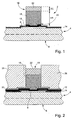
- the semiconductor device 2 partially represented on Figure 1, comprises an integrated circuit 4 in a semiconductor substrate 6.
- a structured metallization layer is deposited with contact pads 8. At least a part of these pads are in electrical contact with external bumps 10, these bumps being used for inner lead bonding in order to interconnect the integrated circuit with a support of the device.
- a barrier layer 12 e.g. of TiW, is sputtered on pad 8 and partially on a passivation layer 14.
- Bump 10 comprises a base layer 18 of a non precious metal, like copper.
- the bottom portion 20 of this base layer 18 comes from a seed layer deposited on barrier layer 12.
- the height HB of the base layer can vary depending on the application, but is preferably greater than ten microns (10 ⁇ m).
- Above base layer 18 is cap layer 22 of a precious metal like gold, i.e. gold or another metal or alloy having similar mechanical and electrical properties to those of gold with regards to bonding of bumps with wires or pads, in particular by metallic joint or with an anisotropic conductive adhesive.
- This cap layer 22 has a thickness TC greater than one micron (1 ⁇ m), preferably between 2 ⁇ m and 5 ⁇ m, and thus has properties relative to bonding conditions which are similar to those of conventional gold bumps.
- integrated circuit 4 is manufactured by a known method.
- a structured metallization layer 8 is deposited in a known manner, e.g. by a PVD process.
- a passivation layer 14 is deposited on the structured layer 8 and apertures are formed in this layer 14 in order to define electrical contact zones for external bumps 10.
- a barrier and adhesion layer 12 is sputtered and a plating base 20 for the following formation of bumps 10 is deposited.
- this plating base is generally made of gold.
- layer 20 is preferably made of a non precious metal, in particular of copper.
- a photoresist mask 26 is deposited and structured in order to form openings for electroplating bumps 10.
- the base layer 18 is electroplated with a non precious metal, in particular copper.
- gold cap layer 22 is then electroplated on top of base layer 18. This subsequent plating is preferably made without any drying step, i.e. by a wet to wet process.
- an electrical voltage may be applied to the semiconductor device before inserting it in the gold plating bath. Thanks to this step in the manufacturing method, base 18 is electrically charged thereby avoiding a dissolution of copper in the gold bath.
- the photoresist mask 26 is eliminated and the barrier layer 12 as well as the seed layer 20 are removed outside bumps zones.
Abstract
The semiconductor device (2) comprises bumps for connecting an integrated circuit to
a support like a glass plate or a flexible film having electrical contact means. The
bumps comprise a base layer (18) of non precious metal, like copper, and a cap layer
of precious metal having gold properties with regards to bonding conditions of the
semiconductor device to the support, the thickness of this cap layer being greater than
1 µm and sufficient to form a functional layer like conventional gold bumps for the
electrical connecting process.
Description
- The present invention concerns the semiconductor domain, and more particularly the bumping technology.
- Bumps formed on semiconductor substrates are commonly used for connecting integrated circuits made in these substrates to supports like glass plates or flexible organic films having electrical paths at their surface. In the case of glass supports, a main assembly method is known as Chip On Glass (COG). In the case of plastic films, a main assembly method is known as Chip On Film (COF). A method similar to COF is also used in the Tape Automatic Bonding technique (TAB), also called Tape Carrier Package (TCP).
- In most applications, gold bumps are now used because gold is an appropriate material for providing a good electrical connection to the support. Different metals, like copper, have also been used as bump material. Although copper is less expensive, it is harder and less ductile than gold. In particular with increasing chip size, bonding conditions with copper could exceed the fracture strength of these more fragile chips. Further, oxidation problems occur with copper. To solve this last particular problem, patent document US 4,005,472 proposes to protect copper bumps with an antioxidant protective coating layer of gold having a thickness of less than 6000 Angstroms (0.6 µm).
- Copper (or copper-nickel) bumps with a thin gold protective layer raise the same problem as copper bumps with regards to their hardness and ductility. For that reason, gold bumps are used since gold has properties well adapted to an efficient interconnecting process in both COG and COF assembly technologies. With gold bumps, a soft interface can be obtained. This soft interface allows in particular high tolerances in the bump height and non planarity of the bonding tool to be compensated.
- In the COF technology, interconnections between the bumps and the film are generally made using copper paths or wires coated with a thin tin layer. The tin of the paths or wires and the gold of the bumps form a gold-tin (Au-Sn) eutectic alloy having a melting point of 280 ° C during inner lead bonding. A sufficient amount of gold (20 % in weight) is required for this purpose. The eutectic alloy defined a soft region which protects the chip against overpressure and thus against damages.
- In the COG technology, an anisotropic conductive adhesive is used for bonding the chip on the electrical paths or pads of the glass layer. This anisotropic conductive adhesive is made of a non conducting adhesive material in which conductive particles are embedded. In order to make an electrical connection between a bump and a path or pad arranged on the glass facing this bump, the conductive particles have to be pressed between the bump and the path or pad until these particles partially penetrate the bump. It is to be noted that the bump upper surface may not be perfectly planar and that the size of the particles may vary. Thus, a certain deformation of the bump is required for achieving a reliable electrical interconnection. For that reason gold presents very good properties for making such interconnections.
- Gold bumping is an established technology. The gold bumps can be formed by electroplating. This technique allows a fine pitch for the bumps arrangement, which is required e.g. for LCD drivers. In the gold bumping industry, the competition has driven the price of bumping step per wafer down. Therefore, cost reduction for manufacturing bumps on semiconductor substrates is now an important issue.
- The object of the present invention is to provide semiconductor devices with connecting bumps which are well suited to the different applications and which can be manufactured at reduced costs.
- For this purpose, the invention concerns a semiconductor device comprising an integrated circuit and bumps electrically connected to the integrated circuit, the bumps being arranged at an external surface of this integrated circuit for interconnecting this integrated circuit to a support having electrical conductive means, characterized in that each of said bumps is formed by a base layer made of a non precious metal, like copper, in electrical contact with said electrical conductive means and by a cap layer of precious metal, like gold, on top of this base layer, the thickness of this cap layer being greater than one micron (1 µm).
- In a preferred embodiment, the thickness of the gold cap layer ranges between 2 µm and 5 µm, this gold cap layer being electroplated on the base layer of the bump.
- Thus, the conventional gold bump is replaced by a bump having composite structure with a base layer formed by a low cost material and a functional gold cap layer. By functional gold cap layer, it is understood a cap layer of gold having, for a given application, enough thickness to provide similar electrical bonding conditions with paths or pads on a support or inner wires extending in an opening of a support compared to conventional gold bumps, in particular a low hardness in the bonding region and a high ductility. Therefore, a bump with a copper base layer and a functional gold cap layer provides gold properties at the bonding interface, which is not the case with a protective anti-corrosion layer having a thickness of less than 6000 Angstroms. A further advantage is that the quantity of gold used will be independent of the height of the bump to be formed, e.g. between 15 µm and 30 µm.
- It is to be noted that the composite structure of the bump can be preferably electroplated using the same photoresist layer thereby maintaining the costs of the process low.
- In a preferred embodiment, the plating base will also be formed of copper (no longer with gold), which results in an even greater cost reduction.
- One preferred embodiment of the semiconductor device according to the present invention and the method of manufacturing such a device will now be described solely by way of example, with reference to the accompanying drawings, in which :
- Figure 1 is a partial cross-section of this preferred embodiment, and
- Figure 2 is a view similar to figure 1, but at an intermediate stage of the manufacturing process of the bumps of the semiconductor device.
- The
semiconductor device 2, partially represented on Figure 1, comprises anintegrated circuit 4 in asemiconductor substrate 6. On top of the integrated circuit, a structured metallization layer is deposited withcontact pads 8. At least a part of these pads are in electrical contact withexternal bumps 10, these bumps being used for inner lead bonding in order to interconnect the integrated circuit with a support of the device. At the bottom of thebump 10, abarrier layer 12, e.g. of TiW, is sputtered onpad 8 and partially on apassivation layer 14. -
Bump 10 comprises abase layer 18 of a non precious metal, like copper. Thebottom portion 20 of thisbase layer 18 comes from a seed layer deposited onbarrier layer 12. The height HB of the base layer can vary depending on the application, but is preferably greater than ten microns (10 µm). Abovebase layer 18 iscap layer 22 of a precious metal like gold, i.e. gold or another metal or alloy having similar mechanical and electrical properties to those of gold with regards to bonding of bumps with wires or pads, in particular by metallic joint or with an anisotropic conductive adhesive. Thiscap layer 22 has a thickness TC greater than one micron (1 µm), preferably between 2 µm and 5 µm, and thus has properties relative to bonding conditions which are similar to those of conventional gold bumps. - Referring now to Figure 2, a method for manufacturing
semiconductor device 2 of Figure 1 will be described. - In
semiconductor substrate 6, integratedcircuit 4 is manufactured by a known method. On top of this circuit, astructured metallization layer 8 is deposited in a known manner, e.g. by a PVD process. Then apassivation layer 14 is deposited on thestructured layer 8 and apertures are formed in thislayer 14 in order to define electrical contact zones forexternal bumps 10. - Then a barrier and
adhesion layer 12 is sputtered and aplating base 20 for the following formation ofbumps 10 is deposited. For conventional gold bumps, this plating base is generally made of gold. But in the case of the present invention,layer 20 is preferably made of a non precious metal, in particular of copper. - In a following step, a
photoresist mask 26 is deposited and structured in order to form openings for electroplatingbumps 10. First, thebase layer 18 is electroplated with a non precious metal, in particular copper. By using the same photoresist mask,gold cap layer 22 is then electroplated on top ofbase layer 18. This subsequent plating is preferably made without any drying step, i.e. by a wet to wet process. - Because copper may dissolve in the gold bath and contaminate it, an electrical voltage may be applied to the semiconductor device before inserting it in the gold plating bath. Thanks to this step in the manufacturing method,
base 18 is electrically charged thereby avoiding a dissolution of copper in the gold bath. - Finally, the
photoresist mask 26 is eliminated and thebarrier layer 12 as well as theseed layer 20 are removed outside bumps zones.
Claims (5)
- Semiconductor device (2) comprising an integrated circuit (4) and bumps (10) electrically connected to the integrated circuit, said bumps being arranged at an external surface of this integrated circuit for interconnecting this integrated circuit to a support having electrical conductive means, characterized in that each of said bumps comprises a base layer (18) made of a non precious metal, like copper, in electrical contact with said electrical contact means and a cap layer (22) of precious metal, like gold, on top of this base.layer, the thickness (TC) of this cap layer being greater than one micron (1 µm).
- Semiconductor device according to claim 1, characterized in that said thickness of said cap layer (22) ranges between 2 µm and 5 µm.
- Semiconductor device according to claim 1 or 2, characterized in that said cap layer (22) is electroplated.
- Semiconductor device according to any one of claims 1 to 3, characterized in that the height (HB) of said base layer is greater than ten microns (10 µm).
- Semiconductor device according to any one of claims 1 to 4, characterized in that it comprises a seed layer (20) arranged at the bottom of said bumps on top of a barrier layer (12), this seed layer being formed of a non precious metal, like copper.
Priority Applications (1)
| Application Number | Priority Date | Filing Date | Title |
|---|---|---|---|
| EP03027257A EP1536469A1 (en) | 2003-11-28 | 2003-11-28 | Semiconductor device with connecting bumps |
Applications Claiming Priority (1)
| Application Number | Priority Date | Filing Date | Title |
|---|---|---|---|
| EP03027257A EP1536469A1 (en) | 2003-11-28 | 2003-11-28 | Semiconductor device with connecting bumps |
Publications (1)
| Publication Number | Publication Date |
|---|---|
| EP1536469A1 true EP1536469A1 (en) | 2005-06-01 |
Family
ID=34442891
Family Applications (1)
| Application Number | Title | Priority Date | Filing Date |
|---|---|---|---|
| EP03027257A Withdrawn EP1536469A1 (en) | 2003-11-28 | 2003-11-28 | Semiconductor device with connecting bumps |
Country Status (1)
| Country | Link |
|---|---|
| EP (1) | EP1536469A1 (en) |
Cited By (23)
| Publication number | Priority date | Publication date | Assignee | Title |
|---|---|---|---|---|
| US7855461B2 (en) | 2003-12-08 | 2010-12-21 | Megica Corporation | Chip structure with bumps and testing pads |
| US7863739B2 (en) | 2001-03-05 | 2011-01-04 | Megica Corporation | Low fabrication cost, fine pitch and high reliability solder bump |
| US7960269B2 (en) | 2005-07-22 | 2011-06-14 | Megica Corporation | Method for forming a double embossing structure |
| US7960270B2 (en) | 2002-01-07 | 2011-06-14 | Megica Corporation | Method for fabricating circuit component |
| US7964973B2 (en) | 2004-08-12 | 2011-06-21 | Megica Corporation | Chip structure |
| US7964961B2 (en) | 2007-04-12 | 2011-06-21 | Megica Corporation | Chip package |
| US7985653B2 (en) | 2005-05-18 | 2011-07-26 | Megica Corporation | Semiconductor chip with coil element over passivation layer |
| US8004092B2 (en) | 2005-10-28 | 2011-08-23 | Megica Corporation | Semiconductor chip with post-passivation scheme formed over passivation layer |
| US8021921B2 (en) | 2002-10-25 | 2011-09-20 | Megica Corporation | Method of joining chips utilizing copper pillar |
| US8022544B2 (en) | 2004-07-09 | 2011-09-20 | Megica Corporation | Chip structure |
| US8021976B2 (en) | 2002-10-15 | 2011-09-20 | Megica Corporation | Method of wire bonding over active area of a semiconductor circuit |
| US8067837B2 (en) | 2004-09-20 | 2011-11-29 | Megica Corporation | Metallization structure over passivation layer for IC chip |
| US8178967B2 (en) | 2001-09-17 | 2012-05-15 | Megica Corporation | Low fabrication cost, high performance, high reliability chip scale package |
| US8193636B2 (en) | 2007-03-13 | 2012-06-05 | Megica Corporation | Chip assembly with interconnection by metal bump |
| US8232192B2 (en) | 2004-05-05 | 2012-07-31 | Megica Corporation | Process of bonding circuitry components |
| US8242601B2 (en) | 2004-10-29 | 2012-08-14 | Megica Corporation | Semiconductor chip with passivation layer comprising metal interconnect and contact pads |
| US8294279B2 (en) | 2005-01-25 | 2012-10-23 | Megica Corporation | Chip package with dam bar restricting flow of underfill |
| US8421227B2 (en) | 2006-06-28 | 2013-04-16 | Megica Corporation | Semiconductor chip structure |
| US8481418B2 (en) | 2002-05-01 | 2013-07-09 | Megica Corporation | Low fabrication cost, high performance, high reliability chip scale package |
| US8558383B2 (en) | 2005-05-06 | 2013-10-15 | Megica Corporation | Post passivation structure for a semiconductor device and packaging process for same |
| US8581404B2 (en) | 2004-07-09 | 2013-11-12 | Megit Acquistion Corp. | Structure of gold bumps and gold conductors on one IC die and methods of manufacturing the structures |
| US8674507B2 (en) | 2003-05-27 | 2014-03-18 | Megit Acquisition Corp. | Wafer level processing method and structure to manufacture two kinds of interconnects, gold and solder, on one wafer |
| US8901733B2 (en) | 2001-02-15 | 2014-12-02 | Qualcomm Incorporated | Reliable metal bumps on top of I/O pads after removal of test probe marks |
Citations (4)
| Publication number | Priority date | Publication date | Assignee | Title |
|---|---|---|---|---|
| EP0766310A2 (en) * | 1995-09-27 | 1997-04-02 | International Business Machines Corporation | Solder bump structure |
| US5656858A (en) * | 1994-10-19 | 1997-08-12 | Nippondenso Co., Ltd. | Semiconductor device with bump structure |
| WO2001056081A1 (en) * | 2000-01-27 | 2001-08-02 | Bookham Technology Plc | Flip-chip bonding arrangement |
| US20030006062A1 (en) * | 2001-07-06 | 2003-01-09 | Stone William M. | Interconnect system and method of fabrication |
-
2003
- 2003-11-28 EP EP03027257A patent/EP1536469A1/en not_active Withdrawn
Patent Citations (4)
| Publication number | Priority date | Publication date | Assignee | Title |
|---|---|---|---|---|
| US5656858A (en) * | 1994-10-19 | 1997-08-12 | Nippondenso Co., Ltd. | Semiconductor device with bump structure |
| EP0766310A2 (en) * | 1995-09-27 | 1997-04-02 | International Business Machines Corporation | Solder bump structure |
| WO2001056081A1 (en) * | 2000-01-27 | 2001-08-02 | Bookham Technology Plc | Flip-chip bonding arrangement |
| US20030006062A1 (en) * | 2001-07-06 | 2003-01-09 | Stone William M. | Interconnect system and method of fabrication |
Cited By (39)
| Publication number | Priority date | Publication date | Assignee | Title |
|---|---|---|---|---|
| US8138079B2 (en) | 1998-12-21 | 2012-03-20 | Megica Corporation | Method of wire bonding over active area of a semiconductor circuit |
| US8901733B2 (en) | 2001-02-15 | 2014-12-02 | Qualcomm Incorporated | Reliable metal bumps on top of I/O pads after removal of test probe marks |
| US8072070B2 (en) | 2001-03-05 | 2011-12-06 | Megica Corporation | Low fabrication cost, fine pitch and high reliability solder bump |
| US7863739B2 (en) | 2001-03-05 | 2011-01-04 | Megica Corporation | Low fabrication cost, fine pitch and high reliability solder bump |
| US8368213B2 (en) | 2001-03-05 | 2013-02-05 | Megica Corporation | Low fabrication cost, fine pitch and high reliability solder bump |
| US9369175B2 (en) | 2001-09-17 | 2016-06-14 | Qualcomm Incorporated | Low fabrication cost, high performance, high reliability chip scale package |
| US8178967B2 (en) | 2001-09-17 | 2012-05-15 | Megica Corporation | Low fabrication cost, high performance, high reliability chip scale package |
| US7960270B2 (en) | 2002-01-07 | 2011-06-14 | Megica Corporation | Method for fabricating circuit component |
| US8461679B2 (en) | 2002-01-07 | 2013-06-11 | Megica Corporation | Method for fabricating circuit component |
| US8890336B2 (en) | 2002-01-07 | 2014-11-18 | Qualcomm Incorporated | Cylindrical bonding structure and method of manufacture |
| US8481418B2 (en) | 2002-05-01 | 2013-07-09 | Megica Corporation | Low fabrication cost, high performance, high reliability chip scale package |
| US9142527B2 (en) | 2002-10-15 | 2015-09-22 | Qualcomm Incorporated | Method of wire bonding over active area of a semiconductor circuit |
| US8026588B2 (en) | 2002-10-15 | 2011-09-27 | Megica Corporation | Method of wire bonding over active area of a semiconductor circuit |
| US8021976B2 (en) | 2002-10-15 | 2011-09-20 | Megica Corporation | Method of wire bonding over active area of a semiconductor circuit |
| US8742580B2 (en) | 2002-10-15 | 2014-06-03 | Megit Acquisition Corp. | Method of wire bonding over active area of a semiconductor circuit |
| US9153555B2 (en) | 2002-10-15 | 2015-10-06 | Qualcomm Incorporated | Method of wire bonding over active area of a semiconductor circuit |
| US8021921B2 (en) | 2002-10-25 | 2011-09-20 | Megica Corporation | Method of joining chips utilizing copper pillar |
| US8421222B2 (en) | 2002-10-25 | 2013-04-16 | Megica Corporation | Chip package having a chip combined with a substrate via a copper pillar |
| US8674507B2 (en) | 2003-05-27 | 2014-03-18 | Megit Acquisition Corp. | Wafer level processing method and structure to manufacture two kinds of interconnects, gold and solder, on one wafer |
| US7855461B2 (en) | 2003-12-08 | 2010-12-21 | Megica Corporation | Chip structure with bumps and testing pads |
| US8232192B2 (en) | 2004-05-05 | 2012-07-31 | Megica Corporation | Process of bonding circuitry components |
| US8581404B2 (en) | 2004-07-09 | 2013-11-12 | Megit Acquistion Corp. | Structure of gold bumps and gold conductors on one IC die and methods of manufacturing the structures |
| US8022544B2 (en) | 2004-07-09 | 2011-09-20 | Megica Corporation | Chip structure |
| US8519552B2 (en) | 2004-07-09 | 2013-08-27 | Megica Corporation | Chip structure |
| US7964973B2 (en) | 2004-08-12 | 2011-06-21 | Megica Corporation | Chip structure |
| US8159074B2 (en) | 2004-08-12 | 2012-04-17 | Megica Corporation | Chip structure |
| US8742582B2 (en) | 2004-09-20 | 2014-06-03 | Megit Acquisition Corp. | Solder interconnect on IC chip |
| US8067837B2 (en) | 2004-09-20 | 2011-11-29 | Megica Corporation | Metallization structure over passivation layer for IC chip |
| US8242601B2 (en) | 2004-10-29 | 2012-08-14 | Megica Corporation | Semiconductor chip with passivation layer comprising metal interconnect and contact pads |
| US8294279B2 (en) | 2005-01-25 | 2012-10-23 | Megica Corporation | Chip package with dam bar restricting flow of underfill |
| US8558383B2 (en) | 2005-05-06 | 2013-10-15 | Megica Corporation | Post passivation structure for a semiconductor device and packaging process for same |
| US7985653B2 (en) | 2005-05-18 | 2011-07-26 | Megica Corporation | Semiconductor chip with coil element over passivation layer |
| US8362588B2 (en) | 2005-05-18 | 2013-01-29 | Megica Corporation | Semiconductor chip with coil element over passivation layer |
| US7960269B2 (en) | 2005-07-22 | 2011-06-14 | Megica Corporation | Method for forming a double embossing structure |
| US8319354B2 (en) | 2005-10-28 | 2012-11-27 | Megica Corporation | Semiconductor chip with post-passivation scheme formed over passivation layer |
| US8004092B2 (en) | 2005-10-28 | 2011-08-23 | Megica Corporation | Semiconductor chip with post-passivation scheme formed over passivation layer |
| US8421227B2 (en) | 2006-06-28 | 2013-04-16 | Megica Corporation | Semiconductor chip structure |
| US8193636B2 (en) | 2007-03-13 | 2012-06-05 | Megica Corporation | Chip assembly with interconnection by metal bump |
| US7964961B2 (en) | 2007-04-12 | 2011-06-21 | Megica Corporation | Chip package |
Similar Documents
| Publication | Publication Date | Title |
|---|---|---|
| EP1536469A1 (en) | Semiconductor device with connecting bumps | |
| US6077726A (en) | Method and apparatus for stress relief in solder bump formation on a semiconductor device | |
| EP1036414B1 (en) | A method of forming a chip scale package using large ductile solder balls | |
| KR100454381B1 (en) | Semiconductor device and manufacturing method thereof | |
| US6650013B2 (en) | Method of manufacturing wire bonded microelectronic device assemblies | |
| US5134460A (en) | Aluminum bump, reworkable bump, and titanium nitride structure for tab bonding | |
| US7554201B2 (en) | Tin-bismuth (Sn-Bi) family alloy solder and semiconductor device using the same | |
| CN101894814B (en) | solder bump UBM structure | |
| JP4334647B2 (en) | Method for forming conductive bumps on a semiconductor device | |
| US7187078B2 (en) | Bump structure | |
| US6864166B1 (en) | Method of manufacturing wire bonded microelectronic device assemblies | |
| US8105934B2 (en) | Bump structure for a semiconductor device and method of manufacture | |
| US8106516B1 (en) | Wafer-level chip scale package | |
| US5597470A (en) | Method for making a flexible lead for a microelectronic device | |
| US20100219528A1 (en) | Electromigration-Resistant Flip-Chip Solder Joints | |
| US20030098513A1 (en) | Method for bonding inner leads to bond pads without bumps and structures formed | |
| US20090160052A1 (en) | Under bump metallurgy structure of semiconductor device package | |
| US7504728B2 (en) | Integrated circuit having bond pad with improved thermal and mechanical properties | |
| US20050151268A1 (en) | Wafer-level assembly method for chip-size devices having flipped chips | |
| US8283756B2 (en) | Electronic component with buffer layer | |
| US6605491B1 (en) | Method for bonding IC chips to substrates with non-conductive adhesive | |
| US7217656B2 (en) | Structure and method for bond pads of copper-metallized integrated circuits | |
| JP2003508898A (en) | Microbeam assembly and internal connection method between integrated circuit and substrate | |
| US20060175711A1 (en) | Structure and method for bonding an IC chip | |
| US5686352A (en) | Method for making a tab semiconductor device with self-aligning cavity and intrinsic standoff |
Legal Events
| Date | Code | Title | Description |
|---|---|---|---|
| PUAI | Public reference made under article 153(3) epc to a published international application that has entered the european phase |
Free format text: ORIGINAL CODE: 0009012 |
|
| AK | Designated contracting states |
Kind code of ref document: A1 Designated state(s): AT BE BG CH CY CZ DE DK EE ES FI FR GB GR HU IE IT LI LU MC NL PT RO SE SI SK TR |
|
| AX | Request for extension of the european patent |
Extension state: AL LT LV MK |
|
| AKX | Designation fees paid | ||
| REG | Reference to a national code |
Ref country code: DE Ref legal event code: 8566 |
|
| STAA | Information on the status of an ep patent application or granted ep patent |
Free format text: STATUS: THE APPLICATION IS DEEMED TO BE WITHDRAWN |
|
| 18D | Application deemed to be withdrawn |
Effective date: 20051202 |