EP1536522A2 - High density connector having a ball type of contact surface - Google Patents
High density connector having a ball type of contact surface Download PDFInfo
- Publication number
- EP1536522A2 EP1536522A2 EP05004456A EP05004456A EP1536522A2 EP 1536522 A2 EP1536522 A2 EP 1536522A2 EP 05004456 A EP05004456 A EP 05004456A EP 05004456 A EP05004456 A EP 05004456A EP 1536522 A2 EP1536522 A2 EP 1536522A2
- Authority
- EP
- European Patent Office
- Prior art keywords
- well
- electrical element
- forming
- electrical
- solder
- Prior art date
- Legal status (The legal status is an assumption and is not a legal conclusion. Google has not performed a legal analysis and makes no representation as to the accuracy of the status listed.)
- Granted
Links
Images

Classifications
-
- H—ELECTRICITY
- H05—ELECTRIC TECHNIQUES NOT OTHERWISE PROVIDED FOR
- H05K—PRINTED CIRCUITS; CASINGS OR CONSTRUCTIONAL DETAILS OF ELECTRIC APPARATUS; MANUFACTURE OF ASSEMBLAGES OF ELECTRICAL COMPONENTS
- H05K3/00—Apparatus or processes for manufacturing printed circuits
- H05K3/30—Assembling printed circuits with electric components, e.g. with resistor
- H05K3/32—Assembling printed circuits with electric components, e.g. with resistor electrically connecting electric components or wires to printed circuits
- H05K3/34—Assembling printed circuits with electric components, e.g. with resistor electrically connecting electric components or wires to printed circuits by soldering
- H05K3/341—Surface mounted components
- H05K3/3421—Leaded components
- H05K3/3426—Leaded components characterised by the leads
-
- H—ELECTRICITY
- H01—ELECTRIC ELEMENTS
- H01R—ELECTRICALLY-CONDUCTIVE CONNECTIONS; STRUCTURAL ASSOCIATIONS OF A PLURALITY OF MUTUALLY-INSULATED ELECTRICAL CONNECTING ELEMENTS; COUPLING DEVICES; CURRENT COLLECTORS
- H01R43/00—Apparatus or processes specially adapted for manufacturing, assembling, maintaining, or repairing of line connectors or current collectors or for joining electric conductors
- H01R43/02—Apparatus or processes specially adapted for manufacturing, assembling, maintaining, or repairing of line connectors or current collectors or for joining electric conductors for soldered or welded connections
- H01R43/0256—Apparatus or processes specially adapted for manufacturing, assembling, maintaining, or repairing of line connectors or current collectors or for joining electric conductors for soldered or welded connections for soldering or welding connectors to a printed circuit board
-
- H—ELECTRICITY
- H01—ELECTRIC ELEMENTS
- H01R—ELECTRICALLY-CONDUCTIVE CONNECTIONS; STRUCTURAL ASSOCIATIONS OF A PLURALITY OF MUTUALLY-INSULATED ELECTRICAL CONNECTING ELEMENTS; COUPLING DEVICES; CURRENT COLLECTORS
- H01R12/00—Structural associations of a plurality of mutually-insulated electrical connecting elements, specially adapted for printed circuits, e.g. printed circuit boards [PCB], flat or ribbon cables, or like generally planar structures, e.g. terminal strips, terminal blocks; Coupling devices specially adapted for printed circuits, flat or ribbon cables, or like generally planar structures; Terminals specially adapted for contact with, or insertion into, printed circuits, flat or ribbon cables, or like generally planar structures
- H01R12/50—Fixed connections
- H01R12/51—Fixed connections for rigid printed circuits or like structures
- H01R12/55—Fixed connections for rigid printed circuits or like structures characterised by the terminals
- H01R12/57—Fixed connections for rigid printed circuits or like structures characterised by the terminals surface mounting terminals
-
- H—ELECTRICITY
- H01—ELECTRIC ELEMENTS
- H01R—ELECTRICALLY-CONDUCTIVE CONNECTIONS; STRUCTURAL ASSOCIATIONS OF A PLURALITY OF MUTUALLY-INSULATED ELECTRICAL CONNECTING ELEMENTS; COUPLING DEVICES; CURRENT COLLECTORS
- H01R12/00—Structural associations of a plurality of mutually-insulated electrical connecting elements, specially adapted for printed circuits, e.g. printed circuit boards [PCB], flat or ribbon cables, or like generally planar structures, e.g. terminal strips, terminal blocks; Coupling devices specially adapted for printed circuits, flat or ribbon cables, or like generally planar structures; Terminals specially adapted for contact with, or insertion into, printed circuits, flat or ribbon cables, or like generally planar structures
- H01R12/70—Coupling devices
- H01R12/71—Coupling devices for rigid printing circuits or like structures
- H01R12/72—Coupling devices for rigid printing circuits or like structures coupling with the edge of the rigid printed circuits or like structures
- H01R12/722—Coupling devices for rigid printing circuits or like structures coupling with the edge of the rigid printed circuits or like structures coupling devices mounted on the edge of the printed circuits
- H01R12/725—Coupling devices for rigid printing circuits or like structures coupling with the edge of the rigid printed circuits or like structures coupling devices mounted on the edge of the printed circuits containing contact members presenting a contact carrying strip, e.g. edge-like strip
-
- H—ELECTRICITY
- H05—ELECTRIC TECHNIQUES NOT OTHERWISE PROVIDED FOR
- H05K—PRINTED CIRCUITS; CASINGS OR CONSTRUCTIONAL DETAILS OF ELECTRIC APPARATUS; MANUFACTURE OF ASSEMBLAGES OF ELECTRICAL COMPONENTS
- H05K2201/00—Indexing scheme relating to printed circuits covered by H05K1/00
- H05K2201/10—Details of components or other objects attached to or integrated in a printed circuit board
- H05K2201/10007—Types of components
- H05K2201/10189—Non-printed connector
-
- H—ELECTRICITY
- H05—ELECTRIC TECHNIQUES NOT OTHERWISE PROVIDED FOR
- H05K—PRINTED CIRCUITS; CASINGS OR CONSTRUCTIONAL DETAILS OF ELECTRIC APPARATUS; MANUFACTURE OF ASSEMBLAGES OF ELECTRICAL COMPONENTS
- H05K2201/00—Indexing scheme relating to printed circuits covered by H05K1/00
- H05K2201/10—Details of components or other objects attached to or integrated in a printed circuit board
- H05K2201/10613—Details of electrical connections of non-printed components, e.g. special leads
- H05K2201/10621—Components characterised by their electrical contacts
- H05K2201/10734—Ball grid array [BGA]; Bump grid array
-
- H—ELECTRICITY
- H05—ELECTRIC TECHNIQUES NOT OTHERWISE PROVIDED FOR
- H05K—PRINTED CIRCUITS; CASINGS OR CONSTRUCTIONAL DETAILS OF ELECTRIC APPARATUS; MANUFACTURE OF ASSEMBLAGES OF ELECTRICAL COMPONENTS
- H05K2201/00—Indexing scheme relating to printed circuits covered by H05K1/00
- H05K2201/10—Details of components or other objects attached to or integrated in a printed circuit board
- H05K2201/10613—Details of electrical connections of non-printed components, e.g. special leads
- H05K2201/10954—Other details of electrical connections
- H05K2201/10984—Component carrying a connection agent, e.g. solder, adhesive
-
- Y—GENERAL TAGGING OF NEW TECHNOLOGICAL DEVELOPMENTS; GENERAL TAGGING OF CROSS-SECTIONAL TECHNOLOGIES SPANNING OVER SEVERAL SECTIONS OF THE IPC; TECHNICAL SUBJECTS COVERED BY FORMER USPC CROSS-REFERENCE ART COLLECTIONS [XRACs] AND DIGESTS
- Y02—TECHNOLOGIES OR APPLICATIONS FOR MITIGATION OR ADAPTATION AGAINST CLIMATE CHANGE
- Y02P—CLIMATE CHANGE MITIGATION TECHNOLOGIES IN THE PRODUCTION OR PROCESSING OF GOODS
- Y02P70/00—Climate change mitigation technologies in the production process for final industrial or consumer products
- Y02P70/50—Manufacturing or production processes characterised by the final manufactured product
Definitions
- the present invention relates to electrical connectors and more particularly to high density I/O connectors such as connectors that are attachable to a circuit substrate by use of a solder ball contact surface.
- the drive to reduce the size of electronic equipment, particularly personal portable devices, and to add additional functions to such equipment has resulted in an ongoing drive for miniaturization of all components, especially electrical connectors.
- Efforts to miniaturize electrical connectors have included reductions in the pitch between terminals in single or double row linear connectors, so that a relatively high number of I/O or other lines can be interconnected by connectors that fit within the tightly circumscribed areas on circuit substrates that are allotted for receiving connectors.
- the drive for miniaturization has also been accompanied by a shift in manufacturing preference to surface mount techniques (SMT) for mounting components on circuit substrates.
- SMT surface mount techniques
- solder ball spherical solder balls attached to the IC package are positioned on electrical contact pads of a circuit substrate to which a layer of solder paste has been applied, typically by use of a screen or mask.
- the unit is then heated to a temperature at which the solder paste and at least a portion of the solder ball melt and fuse to an underlying conductive pad formed on the circuit substrate. This heating process is commonly referred to as solder reflow.
- solder reflow solder reflow
- solder balls and similar systems in connecting ICs to a substrate has many advantages
- a corresponding means for mounting an electrical connector or similar component on a circuit substrate has recently become desirable.
- the use of such techniques in mounting electrical connectors has lagged the use in mounting ICs because the use of solder ball technologies in mounting an electrical connector or similar component to a circuit substrate presents complexities not encountered with IC mounting.
- ICs that have employed solder balls generally present a flat attachment surface.
- connectors usually do not present a flat attachment surface but rather present a series of elongated conductors, commonly referred to as terminal tail ends. Attachment of a solder ball to the small end surface presented by the tip of a terminal tail end presents manufacturing difficulties not present in the attachment of solder balls to a flat surface.
- connectors are generally more susceptible to solder joint stress due to the effects of differential Coefficients of Thermal Expansion (CTE) between the connector and the circuit substrate.
- CTE differential Coefficients of Thermal Expansion
- This susceptibility is primarily due to size and geometry differences between a connector and an IC.
- IC mounting surfaces are generally on the order of 2.5 centimeters square.
- Connector mounting surfaces on the other hand, generally have a narrow width (e.g., 0.5 centimeters or less) and a much longer length (e.g. 5.0 centimeters or more).
- CTE Coefficients of Thermal Expansion
- Connectors attached to circuit substrates via solder ball techniques are also more susceptible to joint stress than a conventional SMT attachment technique.
- a conventional SMT attaches connector terminal tails to a circuit substrate horizontally, providing more attachment surface area for the solder joint.
- the additional surface area of the solder joint in the conventional SMT technique is stronger and, consequently, more tolerant of differences in CTE between the connector, terminal tails and circuit substrate.
- a solder ball connection attaches a connector terminal tail vertically to the circuit substrate with the end of the terminal tail directly mated to the circuit substrate, reducing the amount of attachment surface area.
- differences in CTE are much more likely to stress the terminal tall to circuit substrate joint resulting in failure or quality problems.
- solder balls to attach a connector to a circuit substrate imposes the requirement that the solder balls are coplanar in order to ensure a substantially flat mounting interface.
- the balls will reflow and solder evenly to a planar circuit substrate. Any significant differences in solder coplanarity on a given mounting connection can cause poor soldering performance when the connector is reflowed onto a printed circuit board. Accordingly, users specify very tight coplanarity requirements to achieve high soldering reliability, on the order of 0.1 to 0.2 mm for example.
- the coplanarity requirements can be met and sometimes exceeded.
- the solder ball can absorb variations in terminal tail length by changing shape upon the application of heat to bridge the gaps between the terminal tail ends and the circuit substrate connections.
- the present invention recognizes that there is a need for an improved electrical connector apparatus and accompanying electrical connector construction techniques that address the shortcomings of present electrical connectors.
- the invention meets the above needs by providing an improved electrical connector for use in forming an electrical connection between a contact portion of an electrical component and a contact portion of a circuit substrate and method for constructing the electrical connector.
- the electrical connector comprises a connector body, a plurality of electrical contacts disposed on the connector body and arranged to electrically mate with the contact portion of the electrical component, a plurality of electrical elongated conductors, alternately referred to as terminal tails, disposed on the connector body and arranged to form an electrical connection with the circuit substrate.
- the elongated conductors are in electrical communication with corresponding electrical contacts.
- a substrate contact such as a solder ball, is connected via a butt joint on an end of each of the elongated conductors such that an electrical connection between the elongated conductors and the contact portion of the circuit substrate is selectively accommodated.
- Each of the elongated conductors is disposed in a spacer member passage that has a cross-sectional diameter a little larger than the cross-sectional diameter of the elongated conductor.
- the cross-section is substantially rectangular in shape.
- the passages terminate in wells that are disposed across a planar face of the spacer.
- the wells have a rectangular top opening that is longer along a length of the spacer.
- a portion of the spacer proximate the elongated connector tail end is coated with an anti-migration solution such as oleophobic-hydrophobic flourochemical polymer to assist the process of solder ball formation and attachment.
- One of the primary manufacturing challenges in manufacturing the above described connector involves the method of fusing substrate contact material (e.g., a solder ball) to the end of the tail portion of the elongated conductors.
- the invention accomplishes this attachment task by first forming a well, as described above, within a planar surface of the conductor.
- the planar surface is provided by a spacer member that can be formed separately and attached to the body of the connector or alternatively formed as an integral component with the body.
- the tail ends of the elongated conductors are inserted into passages formed in the spacer member such that the tail ends terminate within a predefined range of the mounting surface and are exposed within the well.
- the well is then filled with solder paste.
- the substrate contacts are fused to the ends of the elongated conductors according to two embodiments.
- a pre-manufactured substrate contact member such as a solder ball is seated into the paste.
- the tail end of the elongated connector, the solder ball (substrate contact member), and solder paste are then heated to a predefined temperature above the melting point of the paste such that the molten solder paste coalesces around the solder board and fuses the solder ball to the elongated conductor end.
- no pre-manufactured substrate contact member is used. Rather, a pre-specified amount of solder paste is applied to and over the well. Thereafter, the tail end and solder paste are heated to a predefined temperature, above the melting point of the solder paste. As a result, the solder paste coalesces into a spherical body attached to the end of the elongated conductor and clear of the well.
- the process for forming a substrate contact on an elongated conductor as described above is further enhanced by coating the well with an anti-migration solution such as oleophobic-hydrophobic fluoropolymer. Thereafter, when the solder paste is heated, the paste is repelled from the treated surfaces of the well and spacer member. This results in a more uniform ball formation.
- the substrate contact attachment process can be further enhanced by passivating a portion of the tail end such that solder paste will not attach to the passivated portion. As a result, the solder can attach only to the very end of the elongated conductor.
- Solder flow restriction at the tail end can be enhanced by passivating the tail end, coating the tail end with an anti-migration solution or both.
- a linear connector having a solder ball type electrical contact surface and methods for attaching the solder balls to the connector will now be described with reference to the Figures.
- an electrical connector is described herein having a substantially rectangular mounting surface wherein the length of the mounting surface is substantially greater than its width.
- the particular dimensions described herein with reference to that connector are merely for the purpose of illustration and are not intended to be limiting.
- the concepts disclosed herein have a broader application to a much wider variation of connector mounting surface geometries.
- the concepts disclosed with reference to this connector could be employed, for example, with a connector having a connection mounting surface having a more square or radial geometry.
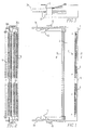
- connector 1 comprises a connector body 5, a plurality of elongated conductors 8, an interface or spacer member 10, electrical element contacts 9, hold down element 13 with an upwardly extending arm 15 and connector latches 24.
- the front of connector 1 comprises a plurality of electrical contacts 9 arranged within two openings, which are designed to selectively engage and mate with corresponding electrical contacts for an electrical element such as those electrical contacts present on a daughter board.
- each electrical contact 9 is in electrical communication with a corresponding elongated conductor 8 such that a current flow path is established therebetween.
- Elongated conductors 8 are designed for permanent connection to electrical contacts on a circuit substrate (not shown). Thereafter, electrical communication can be selectively established between an electrical element inserted into electrical connector 1 and a circuit substrate to which it is attached.
- electrical connector 1 can be connected to a circuit substrate such as a card edge connector of the type used in a computer motherboard. Thereafter, a user, via attached electrical connector 1, can selectively add a daughter board or boards (e.g., memory modules) to the computer motherboard.
- the electrical contacts 9 of connector 1 comprise a linear array stacked in two parallel rows 36A and 36B, each row accepting a single daughter board.
- a user inserts an electrical element laterally into connector 1.
- connector latches 24 that correspond to the particular row, 36A or 36B, engage and lock the electrical element into place on connector 1.
- two parallel rows are shown with respect to connector 1, the concepts disclosed herein are equally applicable to a connector having one row, three rows and so on.
- connector body 5 and connector latches 24 are constructed from a molded plastic material to reduce weight.
- connector 1 further comprises stacked insert molded wafers 2, which are locked together in a pin and socket arrangement 4.
- wafers 2 are retained in housing 5 by a series of dimples 6 which are fitted into cylindrical openings 7.
- a plurality of elongated conductors 8 extend into each of wafers 2.
- Each elongated conductor therein joins in electrical communication with a corresponding electrical contact 9.
- Each elongated conductor 8 also extends out from wafer 2 and into spacer member 10.
- a bend 29, preferably about 90 degrees in the disclosed embodiment, along with the length of elongated conductor 8 allows connector 1 to provide interfaces on two different planes.
- the bend allows connector 1 to interface vertically with respect to the board, while interfacing with an electrical element that is positioned horizontally with respect to the board.
- the electrical element projects horizontally over the circuit substrate surface conserving circuit substrate height.
- Other degrees of bends 29 could be used as required to adjust to a variety of application geometries without departing from the inventive aspects of the present invention.
- the elongated conductors could have no bend, in which case, the electrical element would project vertically with respect to the circuit substrate.
- each elongated conductor 8 extends through a corresponding passage 25 in spacer member 10 and is terminated by a substrate contact 12 such as a solder ball.
- a substrate contact 12 such as a solder ball.
- Each elongated conductor 8 preferably has a substantially rectangular cross-sectional shape such as a square; however, other cross-sectional shapes such as round may function equally as well.
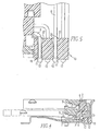
- Figure 5 presents a more detailed view of elongated conductors 8 in relation to spacer member 10.
- Spacer member 10 can be a separate component that is attached to connector body 5 or, alternatively, could be integrally formed therewith.
- spacer member 10 has a plurality of passages 25, one passage 25 being provided to guide and support one tail end of each elongated conductor 8 disposed within a passage 25.
- the diameter of passage 25 is a little larger than the diameter of elongated conductor 8.
- the tail end of elongated conductor 8 is disposed within passage 25 such that clearance 18 is provided between the sides of elongated conductor 8 and the walls of passage 25.
- passage 25 has a width of about 0.38 mm.
- Clearance 18 provides an important feature in tolerating differences in Coefficients of Thermal Expansion (CTE) between the material forming the spacer member 10 and the material forming the circuit substrate on which the connector is mounted. That is, passages 25 are sized to provide guidance to elongated conductors 8 during substrate contact 12 attachment and further during connector 1 attachment to a circuit substrate.
- elongated conductors 8 have a clearance with and are not physically connected to spacer member 10, permitting spacer member 10 to expand and contract without the side walls of the passages 25 impinging upon elongated conductors 8 because of the clearance.
- Passage 25 preferably comprises a cross-section substantially similar to the cross-section of elongated conductor 8. For example, if elongated conductor 8 has a substantially rectangular cross-section then passage 25 also has a substantially rectangular cross-section. Each passage 25 terminates in the bottom of well 11 and includes a wide inlet cavity 27 that provides guidance to elongated conductor 8 during insertion into spacer member 10.
- Each end of a conductor 8 terminates within well 11 and therein is fused to a substrate contact 12, which is also partially disposed within well 11.
- a substrate contact 12 which is also partially disposed within well 11.
- the termination height of the elongated conductors 8 within wells 11 will vary among conductors 8. This height variation is commonly referred to as coplanarity.
- well 11 is substantially rectangular in cross-section having a length 1 slightly larger than a width w.
- width w is preferably 0.5 mm; whereas, length 1 is preferably 0.55 mm.
- substrate contact 12 is on the order of .3 mm to .5 mm.
- the rectangular shape of well 11 also accommodates effects of thermal expansion and contraction. The clearance between the sides of well 11 and substrate contact 12 ensures that well 11 will not impinge upon the solder joint during expansion and contraction.
- the length of well 11 is aligned with the length of spacer member 10 to accommodate thermal cycles while maximizing conductor 8 density. Because spacer member 10 is longer along its length than its width, the effects of expansion and contraction will be correspondingly greater along the length of spacer member 10 than along the width. Accordingly, a top opening of well 11 has dimensions that accommodate the lengthwise thermal expansion and contraction. Along the width of spacer member 10, the effects of expansion and contraction are less of an issue because of the smaller size relative to the length. Consequently, the width of well 11 can be narrower than the length.
- the overall result is a well 11 that is sized to accommodate expansion and contraction along the length of connector 1 while allowing a higher density of wells 11 and conductors 8 along the width of connector 1.
- the top opening of well 11 is dimensioned in this way, tighter elongated conductor 8 densities across the width of spacer member 10 are possible while allowing well 11 to maintain a required volume of solder paste during substrate contact attachment.
- FIG. 6 an embodiment of the attachment of substrate contact 12 to end of the elongated conductor 8 is shown.
- the substrate contact 12 is fused to the end of elongated conductor 8 with a butt joint.
- a portion of the tail end of each elongated conductor 8 has a passivated surface 17.
- Passivated surface 17 ensures that molten solder, used during the attachment process, does not wick along the sides of elongated conductor 8 and potentially enter clearance 18 during substrate contact reflow. As described above, clearance 18 accommodates differences in Coefficients of Thermal Expansion.
- an anti-solder wicking or non-solder wettable material is applied to the surface 17.
- One preferred material for this purpose is nickel plating. While not intending to be bound by any particular theory, it is believed that the solder resistant feature of this nickel plated area results from or is enhanced by the oxidation of the nickel plating, for example, by laser oxidation, steam exposure or ambient air exposure. Other solder wick resistant materials are believed to be useable for this purpose, such as fluorine containing solder resist coatings. Alternatively, a combination of nickel and fluorine could be used.
- Figure 7 depicts a second embodiment of the substrate contact and elongated conductor 8 interface.
- the end of elongated conductor 8 is beveled.
- solder filet 21 is formed between substrate contact 12 and the end of elongated conductor 8 during the attachment of substrate contact 12 to elongated conductor 8.
- This second embodiment also reduces the potential for solder to wick into the clearance 18 by capturing solder within a bevel.
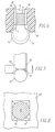
- each well 11 is substantially uniform in size and shape and provides several features of importance with respect to the present invention. Referring to Figure 9, for example, each well 11 ensures that a generally uniform amount of solder paste 19 is received therein using a process such as a simple deposit and squeegee operation. Thus, the amount of solder available for securing each solder ball (substrate contact 12) onto an end of elongated conductor 8 is substantially uniform.
- the wells 11 locate the position of each substrate contact in the lateral X-Y directions prior to attachment of the substrate contacts in the Z direction with respect to the bottom surface of spacer member 10 and the end of elongated conductor 8.After solder reflow, as best shown in Figure 6, the solder contained in paste 19 in well 11 increases the solder ball (substrate contact 12) size by area 16.
- the size of area 16 is affected by the height of the tip of conductor 8 within well 11.
- the amount of solder paste 19 deposited in each well 11 is altered by the variation in elongated conductor 8 height. For example, a conductor 8 tip that is higher in well 11 will displace more solder paste; whereas, a conductor 8 tip that is lower in well 11 will displace less solder paste. If less paste is available in the well, during reflow of the solder paste less paste is available to coalesce around the substrate contact, resulting in a slightly smaller substrate contact 12. A smaller substrate contact will result in a lower contact height. On the other hand, when more paste is available in the well a larger substrate contact will result, corresponding to a higher substrate contact height.
- the process above describes a substrate contact attachment via the use of preformed substrate contacts 12 such as solder balls.
- the substrate contact interface can be formed without the use of preformed substrate contacts.
- Figure 10 there is shown a method of substrate contact 12 attachment using only solder paste.
- a pre-specified amount of solder paste 19A is deposited in and over well 11.
- This pre-specified amount of solder paste can be deposited by a commercial dispensing machine such as a CAM/A LOT 1818 available from Camelot Systems, Inc. After the solder paste deposition, the connector is heated above the solder paste melting point.
- the solder within the paste then coalesces into a substrate contact 16A, which forms on the end of elongated conductor 8.As described above with reference to the preformed substrate contact technique, the variable volume of paste in the well 11 will effect the size and coplanarity of the resultant substrate contacts. Similar to the preformed substrate contact method, the displacement of solder paste by the height of conductor 8 within well 11 will affect the final coplanarity in this method as well.
- coplanarity of the substrate mounting face of a connector utilizing substrate contact mounting is critical with any SMT device.
- connector 1 there are two primary factors that influence the coplanarity of the connector to circuit substrate interface: (1) the coplanarity of the end surfaces, i.e., the tips, of elongated conductors 8; and (2) the coplanarity of substrate contacts 12.
- the coplanarity of the tips of elongated conductors 8 is affected by a variety of factors such as length of the conductor 8, uniformity of the bends, the ability to keep the conductors consistently parallel and the like.
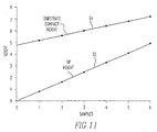
- FIG 11 there is shown an exemplary graph of the coplanarity of the tips of elongated conductors 8 before the attachment of substrate contacts 12 (curve 32) versus the coplanarity of elongated conductors 8 with the attached substrate contacts 12 (curve 34).
- the units along the abscissa represents different samples used in the coplanarity measurement.
- the units along the ordinate represent unit sample height labeled 0, 1, 2 and so on; however, these units are labeled to merely illustrate the relative relationship between the tip position and corresponding substrate contact height. Actual units and values will vary depending on factors such as well dimensions and substrate contact size.
- Curve 32 represents the height of an elongated conductor tip as measured above the bottom of well 11 (see also Figure 6). Thus, at sample 0, for example, the measured tip height is 0 units. At sample 1, the tip height is about 0.75 and so on. At sample 5, the tip height is about 4 units.
- Curve 34 represents the height above the bottom of well 11 of the same tip after attachment of the substrate contact 12 (see also Figure 6).
- the corresponding height after attachment of substrate contact 12 is about 4.5 units.
- the corresponding substrate contact height is about 5 units and so on.
- the substrate contact height is about than 6.5 units.
- Comparing the curves 32 and 34 illustrates that the process of attaching substrate contact 12 to the end of conductor 8 absorbs some of the variations in coplanarity of the tips of conductors 8.
- the difference between the tip height (preattachment curve 32) and the substrate contact height (post attachment curve 34) is about 4.5 units.
- the tip height is about 4 units
- the substrate contact height is about 6.5 units, for a difference of only 2.5 unit.
- the total change in tip height over the entire range of samples was about 4 units, but the total change of substrate contact height over the same sample range was only about 2 units.
- a typical connector before substrate contact attachment will have a number of elongated conductors 8 with different tip heights. If, for example, one conductor 8 has a tip height of 0 (i.e., the tip is exactly flush with the bottom of the well) and another connector has a tip height of 4 units, the coplanarity between the tips would be about 4 units. Under some circumstances this coplanarity variation of 4 units may be unacceptable. However, after the attachment of substrate contacts 12 according to the methods described herein, the corresponding substrate contact heights will be 4.5 units and 6.5 units respectively, for a final coplanarity of about 2 units. Significantly, the final coplanarity is only 2 units versus 4 units.
- a connector 1 can be constructed with a higher tolerance for elongated conductors coplanarity than would be possible otherwise.
- the quality of substrate contact 12 attachment is enhanced by the application of an anti-migration or anti-wicking solution to an area in and around well 11.
- an anti-migration or anti-wicking solution to an area in and around well 11.
- substrate contacts may form unevenly, sometimes wicking to the well edges.
- solder is repelled from the well edges and forms more uniform substrate contacts on the ends of elongated conductors 8.
- the preferred anti-migration solution is oleophobic-hydrophobic fluoropolymer. Such a solution is commercial available from 3M corporation under the Fluorad brand name.
- the substrate contact will preferably be a solder ball.
- the fusible element can also have a shape other than a sphere.
- the ends of elongated conductors 8 will extend into well 11 by a sufficient amount to present adequate surface area for the substrate contact to fuse to, and will usually preferably extend into the well from about 25 percent to 75 percent and more preferably to about 50 percent of the depth of the well as previously mentioned.
- the well ordinarily will be circular, square or the shape of any other regular polygon in cross-section.
- the conductive element When the conductive element is solder, it will preferably be an alloy which is in the range of about 10% Sn and 90% Pb to about 90% Sn and 10% Pb. More preferably the alloy will be eutectic which is 63% Sn and 37% Pb and has a melting point of 183 degrees C.
- a "hard” solder alloy with a higher lead content would be used for mating to materials such as ceramics.
- the "hard” substrate contact will “mushroom” or deform slightly as it softens under typical SMT conditions, but will not melt.
- a “soft” eutectic ball is used for attachment to printed circuit boards and will usually reflow and reform itself under typical SMT conditions.
- Other solders known to be suitable for electronic purposes are also believed to be acceptable for use in this method. Such solders include, without limitation, electronically acceptable tin-antimony, tin-silver and lead silver alloys and indium.
- a body of material which is not fusible at SMT temperatures may be attached by reflow of the solder paste in the well onto the contacts.
- the connector mounting interface would comprise a plurality of infusible spheres in a tightly coplanar array. Such a connector would be secured on a substrate by conventional SMT techniques.
- solder paste or cream incorporating any conventional organic or inorganic solder flux may be adapted for use in this method, a no clean solder paste or cream is preferred.
- solder pastes or creams would include a solder alloy in the form of a fine powder suspended in a suitable fluxing material.
- This powder will ordinarily be an alloy and not a mixture of constituents.
- the ratio of solder to flux will ordinarily be high and in the range of 80% - 95% by weight solder or approximately 50% by volume.
- a solder cream will be formed when the solder material is suspended in a rosin flux.
- the rosin flux will be a white rosin or a low activity rosin flux, although for various purposes activated or superactivated rosins may be used.
- a solder paste will be formed when a solder alloy in the form of a fine powder is suspended in an organic acid flux or an inorganic acid flux.
- Such organic acids may be selected from lactic, oleic, stearic, phthalic, citric or other similar acids.
- Such inorganic acids may be selected from hydrochloric, hydrofluoric and orthophosphoric acid.
- Cream or paste may be applied by brushing, screening, or extruding onto the surface which may advantageously have been gradually preheated to ensure good we
- Heating is preferably conducted in a panel infra red (IR) solder reflow conveyor oven.
- the connector would then be heated to a temperature above the melting point of the solder within the solder paste
Abstract
Description
- The present invention relates to electrical connectors and more particularly to high density I/O connectors such as connectors that are attachable to a circuit substrate by use of a solder ball contact surface.
- The drive to reduce the size of electronic equipment, particularly personal portable devices, and to add additional functions to such equipment has resulted in an ongoing drive for miniaturization of all components, especially electrical connectors. Efforts to miniaturize electrical connectors have included reductions in the pitch between terminals in single or double row linear connectors, so that a relatively high number of I/O or other lines can be interconnected by connectors that fit within the tightly circumscribed areas on circuit substrates that are allotted for receiving connectors. The drive for miniaturization has also been accompanied by a shift in manufacturing preference to surface mount techniques (SMT) for mounting components on circuit substrates. The confluence of the increasing use of SMT and the required fine pitch of linear connectors has resulted in approaching the high volume, low cost limits of SMT for mounting connectors that employ presently available mounting designs. The limit is being reached because further reductions in pitch of the terminals greatly increase the risk of bridging adjacent solder pads or terminals during reflow of the solder paste. Array electrical connectors have been proposed to satisfy the need for increased I/O density. Such electrical connectors have a two dimensional array of terminal tails and can provide improved density. However, these connectors present certain difficulties with respect to attachment to the circuit substrate by SMT techniques because the surface mount tails of most, if not all, of the terminals must be attached beneath the connector body. As a result, the mounting techniques used must be highly reliable because of the difficulty in visually inspecting the solder connections and repairing them, if faulty.
- Mounting techniques for other electronic components have addressed the reliability of solder connections in hard to inspect positions. For example, integrated circuit (IC) mounting to plastic or ceramic substrates have increasingly employed solder balls and other similar packages to provide such a reliable attachment. In a solder ball technique, spherical solder balls attached to the IC package are positioned on electrical contact pads of a circuit substrate to which a layer of solder paste has been applied, typically by use of a screen or mask. The unit is then heated to a temperature at which the solder paste and at least a portion of the solder ball melt and fuse to an underlying conductive pad formed on the circuit substrate. This heating process is commonly referred to as solder reflow. The IC is thereby connected to the substrate without need of external leads on the IC.
- While the use of solder balls and similar systems in connecting ICs to a substrate has many advantages, a corresponding means for mounting an electrical connector or similar component on a circuit substrate has recently become desirable. The use of such techniques in mounting electrical connectors has lagged the use in mounting ICs because the use of solder ball technologies in mounting an electrical connector or similar component to a circuit substrate presents complexities not encountered with IC mounting. For example, ICs that have employed solder balls generally present a flat attachment surface. By contrast, connectors usually do not present a flat attachment surface but rather present a series of elongated conductors, commonly referred to as terminal tail ends. Attachment of a solder ball to the small end surface presented by the tip of a terminal tail end presents manufacturing difficulties not present in the attachment of solder balls to a flat surface.
- In addition to the manufacturing difficulties, connectors are generally more susceptible to solder joint stress due to the effects of differential Coefficients of Thermal Expansion (CTE) between the connector and the circuit substrate. This susceptibility is primarily due to size and geometry differences between a connector and an IC. For example, IC mounting surfaces are generally on the order of 2.5 centimeters square. Connector mounting surfaces, on the other hand, generally have a narrow width (e.g., 0.5 centimeters or less) and a much longer length (e.g. 5.0 centimeters or more). Primarily because of the relatively long length of the connector, differences in CTE between a connector and a circuit substrate potentially have a much greater effect on the solder joints than the differences in CTE between an IC and a circuit substrate.
- Connectors attached to circuit substrates via solder ball techniques are also more susceptible to joint stress than a conventional SMT attachment technique. For example, a conventional SMT attaches connector terminal tails to a circuit substrate horizontally, providing more attachment surface area for the solder joint. The additional surface area of the solder joint in the conventional SMT technique is stronger and, consequently, more tolerant of differences in CTE between the connector, terminal tails and circuit substrate. A solder ball connection, on the other hand, attaches a connector terminal tail vertically to the circuit substrate with the end of the terminal tail directly mated to the circuit substrate, reducing the amount of attachment surface area. As a result of the smaller attachment surface, differences in CTE are much more likely to stress the terminal tall to circuit substrate joint resulting in failure or quality problems.
- Furthermore, in most circuit substrate applications, the electrical component mounting surfaces of the surface mount connections must meet strict coplanarity requirements. Thus, the use of solder balls to attach a connector to a circuit substrate imposes the requirement that the solder balls are coplanar in order to ensure a substantially flat mounting interface. Thus, in the final application the balls will reflow and solder evenly to a planar circuit substrate. Any significant differences in solder coplanarity on a given mounting connection can cause poor soldering performance when the connector is reflowed onto a printed circuit board. Accordingly, users specify very tight coplanarity requirements to achieve high soldering reliability, on the order of 0.1 to 0.2 mm for example. By providing a connection using a solder ball technique, the coplanarity requirements can be met and sometimes exceeded. Unlike conventional SMT, the solder ball can absorb variations in terminal tail length by changing shape upon the application of heat to bridge the gaps between the terminal tail ends and the circuit substrate connections.
- The present invention recognizes that there is a need for an improved electrical connector apparatus and accompanying electrical connector construction techniques that address the shortcomings of present electrical connectors.
- The invention meets the above needs by providing an improved electrical connector for use in forming an electrical connection between a contact portion of an electrical component and a contact portion of a circuit substrate and method for constructing the electrical connector. The electrical connector comprises a connector body, a plurality of electrical contacts disposed on the connector body and arranged to electrically mate with the contact portion of the electrical component, a plurality of electrical elongated conductors, alternately referred to as terminal tails, disposed on the connector body and arranged to form an electrical connection with the circuit substrate. The elongated conductors are in electrical communication with corresponding electrical contacts.A substrate contact, such as a solder ball, is connected via a butt joint on an end of each of the elongated conductors such that an electrical connection between the elongated conductors and the contact portion of the circuit substrate is selectively accommodated.
- Each of the elongated conductors is disposed in a spacer member passage that has a cross-sectional diameter a little larger than the cross-sectional diameter of the elongated conductor. As a result, clearance is provided between the sides of the electrical conductor and the side walls of the passage. Preferably, the cross-section is substantially rectangular in shape. The passages terminate in wells that are disposed across a planar face of the spacer. The wells have a rectangular top opening that is longer along a length of the spacer. Moreover, a portion of the spacer proximate the elongated connector tail end is coated with an anti-migration solution such as oleophobic-hydrophobic flourochemical polymer to assist the process of solder ball formation and attachment.
- One of the primary manufacturing challenges in manufacturing the above described connector involves the method of fusing substrate contact material (e.g., a solder ball) to the end of the tail portion of the elongated conductors. The invention accomplishes this attachment task by first forming a well, as described above, within a planar surface of the conductor. Here, the planar surface is provided by a spacer member that can be formed separately and attached to the body of the connector or alternatively formed as an integral component with the body. In either case, the tail ends of the elongated conductors are inserted into passages formed in the spacer member such that the tail ends terminate within a predefined range of the mounting surface and are exposed within the well. The well is then filled with solder paste. Finally, the substrate contacts are fused to the ends of the elongated conductors according to two embodiments.
- In the first embodiment, a pre-manufactured substrate contact member such as a solder ball is seated into the paste. The tail end of the elongated connector, the solder ball (substrate contact member), and solder paste are then heated to a predefined temperature above the melting point of the paste such that the molten solder paste coalesces around the solder board and fuses the solder ball to the elongated conductor end.
- According to a second embodiment, no pre-manufactured substrate contact member is used. Rather, a pre-specified amount of solder paste is applied to and over the well. Thereafter, the tail end and solder paste are heated to a predefined temperature, above the melting point of the solder paste. As a result, the solder paste coalesces into a spherical body attached to the end of the elongated conductor and clear of the well.
- The process for forming a substrate contact on an elongated conductor as described above is further enhanced by coating the well with an anti-migration solution such as oleophobic-hydrophobic fluoropolymer. Thereafter, when the solder paste is heated, the paste is repelled from the treated surfaces of the well and spacer member. This results in a more uniform ball formation. The substrate contact attachment process can be further enhanced by passivating a portion of the tail end such that solder paste will not attach to the passivated portion. As a result, the solder can attach only to the very end of the elongated conductor. Solder flow restriction at the tail end can be enhanced by passivating the tail end, coating the tail end with an anti-migration solution or both.
- The method and connector of the present invention is further described with reference to the accompanying drawings in which:
- FIG. 1
- is a top plan view of a card edge connector which represents a preferred embodiment of the connector of the present invention;
- FIG. 2
- is a front view of the card edge connector shown in FIG. 1;
- FIG. 3
- is a side view of the card edge connector shown in FIG. 1;
- FIG. 4
- is a cross-sectional view through 4-4 in FIG. 1;
- FIG. 5
- is a detailed view of the substrate contact area of FIG. 4;
- FIG. 6
- is a schematic cross-sectional view of completed substrate contact connection to a first tail end embodiment;
- FIG. 7
- is a schematic cross-sectional view of a completed substrate contact connection to a first tail end embodiment;
- FIG. 8
- is a bottom plan view of a substrate contact connection;
- FIG. 9
- is a schematic cross-sectional view of a substrate contact connection according to a first method;
- FIG.10
- is a schematic cross-sectional view of a substrate contact connection according to a second method; and
- FIG.11
- is a graph comparing relative terminal tail height versus substrate contact height.
- According to presently preferred embodiments, a linear connector having a solder ball type electrical contact surface and methods for attaching the solder balls to the connector will now be described with reference to the Figures. It will be appreciated by those of ordinary skill in the art that the description given herein with respect to those Figures is for exemplary purposes only and is not intended in any way to limit the scope of the invention. For example, an electrical connector is described herein having a substantially rectangular mounting surface wherein the length of the mounting surface is substantially greater than its width. However, the particular dimensions described herein with reference to that connector are merely for the purpose of illustration and are not intended to be limiting. The concepts disclosed herein have a broader application to a much wider variation of connector mounting surface geometries. The concepts disclosed with reference to this connector could be employed, for example, with a connector having a connection mounting surface having a more square or radial geometry.
- Referring now to Figures 1-3, there is shown top, front and side views, respectively, of an
electrical connector 1 of the present invention. As shown,connector 1 comprises aconnector body 5, a plurality ofelongated conductors 8, an interface orspacer member 10,electrical element contacts 9, hold downelement 13 with an upwardly extendingarm 15 and connector latches 24. As best shown in Figure 2, the front ofconnector 1 comprises a plurality ofelectrical contacts 9 arranged within two openings, which are designed to selectively engage and mate with corresponding electrical contacts for an electrical element such as those electrical contacts present on a daughter board. As is described in further detail below, eachelectrical contact 9 is in electrical communication with a correspondingelongated conductor 8 such that a current flow path is established therebetween.Elongated conductors 8 are designed for permanent connection to electrical contacts on a circuit substrate (not shown). Thereafter, electrical communication can be selectively established between an electrical element inserted intoelectrical connector 1 and a circuit substrate to which it is attached. In this way, for example,electrical connector 1 can be connected to a circuit substrate such as a card edge connector of the type used in a computer motherboard. Thereafter, a user, via attachedelectrical connector 1, can selectively add a daughter board or boards (e.g., memory modules) to the computer motherboard. - The
electrical contacts 9 ofconnector 1 comprise a linear array stacked in two parallel rows 36A and 36B, each row accepting a single daughter board. A user inserts an electrical element laterally intoconnector 1. As each daughter board is inserted, connector latches 24 that correspond to the particular row, 36A or 36B, engage and lock the electrical element into place onconnector 1. Although two parallel rows are shown with respect toconnector 1, the concepts disclosed herein are equally applicable to a connector having one row, three rows and so on. Preferably,connector body 5 and connector latches 24 are constructed from a molded plastic material to reduce weight. - Further details of the arrangement of
connector 1 can be seen with reference to Figure 4. Figure 4 presents a cross-sectional view ofconnector 1 taken along the line 4-4. As shown therein,connector 1 further comprises stacked insert moldedwafers 2, which are locked together in a pin andsocket arrangement 4. Thus locked together;wafers 2 are retained inhousing 5 by a series ofdimples 6 which are fitted intocylindrical openings 7. A plurality ofelongated conductors 8 extend into each ofwafers 2. Each elongated conductor therein joins in electrical communication with a correspondingelectrical contact 9. Eachelongated conductor 8 also extends out fromwafer 2 and intospacer member 10. Abend 29, preferably about 90 degrees in the disclosed embodiment, along with the length ofelongated conductor 8 allowsconnector 1 to provide interfaces on two different planes.For example, the bend allowsconnector 1 to interface vertically with respect to the board, while interfacing with an electrical element that is positioned horizontally with respect to the board. As such, the electrical element projects horizontally over the circuit substrate surface conserving circuit substrate height. Other degrees ofbends 29 could be used as required to adjust to a variety of application geometries without departing from the inventive aspects of the present invention. For example, the elongated conductors could have no bend, in which case, the electrical element would project vertically with respect to the circuit substrate. The tail end of eachelongated conductor 8 extends through acorresponding passage 25 inspacer member 10 and is terminated by asubstrate contact 12 such as a solder ball. Eachelongated conductor 8 preferably has a substantially rectangular cross-sectional shape such as a square; however, other cross-sectional shapes such as round may function equally as well. - Figure 5 presents a more detailed view of
elongated conductors 8 in relation tospacer member 10.Spacer member 10 can be a separate component that is attached toconnector body 5 or, alternatively, could be integrally formed therewith. As shown,spacer member 10 has a plurality ofpassages 25, onepassage 25 being provided to guide and support one tail end of eachelongated conductor 8 disposed within apassage 25. Significantly, the diameter ofpassage 25 is a little larger than the diameter ofelongated conductor 8. Accordingly, the tail end ofelongated conductor 8 is disposed withinpassage 25 such thatclearance 18 is provided between the sides ofelongated conductor 8 and the walls ofpassage 25. For example, whereaselongated conductor 8 has a width of about 0.305 mm,passage 25 has a width of about 0.38 mm.Clearance 18 provides an important feature in tolerating differences in Coefficients of Thermal Expansion (CTE) between the material forming thespacer member 10 and the material forming the circuit substrate on which the connector is mounted. That is,passages 25 are sized to provide guidance toelongated conductors 8 duringsubstrate contact 12 attachment and further duringconnector 1 attachment to a circuit substrate. However, elongatedconductors 8 have a clearance with and are not physically connected tospacer member 10, permittingspacer member 10 to expand and contract without the side walls of thepassages 25 impinging uponelongated conductors 8 because of the clearance. The amount of clearance is related to the differential in CTE noted above. As a result, stress is reduced in a solder joint betweenelongated conductors 8 and the circuit substrate during thermal expansion and contraction cycles.Passage 25 preferably comprises a cross-section substantially similar to the cross-section ofelongated conductor 8. For example, ifelongated conductor 8 has a substantially rectangular cross-section thenpassage 25 also has a substantially rectangular cross-section. Eachpassage 25 terminates in the bottom of well 11 and includes awide inlet cavity 27 that provides guidance toelongated conductor 8 during insertion intospacer member 10. Each end of aconductor 8 terminates within well 11 and therein is fused to asubstrate contact 12, which is also partially disposed within well 11.For a variety of reasons, including the bend inelongated conductors 8, the termination height of theelongated conductors 8 withinwells 11 will vary amongconductors 8. This height variation is commonly referred to as coplanarity. - Referring now to Figure 8, a bottom plan view of a
substrate contact 12 in relation to well 11 is depicted. As shown, well 11 is substantially rectangular in cross-section having alength 1 slightly larger than a width w. For example, width w is preferably 0.5 mm; whereas,length 1 is preferably 0.55 mm. Additionally, according to a first embodiment,substrate contact 12 is on the order of .3 mm to .5 mm. Thus, there is a clearance of at least about 0.05 mm betweensubstrate contact 12 and two sides of well 11. As withpassages 25, the rectangular shape of well 11 also accommodates effects of thermal expansion and contraction. The clearance between the sides of well 11 andsubstrate contact 12 ensures that well 11 will not impinge upon the solder joint during expansion and contraction. - The length of
well 11 is aligned with the length ofspacer member 10 to accommodate thermal cycles while maximizingconductor 8 density. Becausespacer member 10 is longer along its length than its width, the effects of expansion and contraction will be correspondingly greater along the length ofspacer member 10 than along the width. Accordingly, a top opening of well 11 has dimensions that accommodate the lengthwise thermal expansion and contraction. Along the width ofspacer member 10, the effects of expansion and contraction are less of an issue because of the smaller size relative to the length. Consequently, the width of well 11 can be narrower than the length. The overall result is a well 11 that is sized to accommodate expansion and contraction along the length ofconnector 1 while allowing a higher density ofwells 11 andconductors 8 along the width of connector 1.Additionally, because the top opening of well 11 is dimensioned in this way, tighterelongated conductor 8 densities across the width ofspacer member 10 are possible while allowing well 11 to maintain a required volume of solder paste during substrate contact attachment. - Further details of the connection of
substrate contacts 12 toelongated connectors 8 will now be described with reference to Figures 6-9. Referring now to Figure 6, an embodiment of the attachment ofsubstrate contact 12 to end of theelongated conductor 8 is shown. Thesubstrate contact 12 is fused to the end ofelongated conductor 8 with a butt joint. To ensure a quality butt joint betweensubstrate contact 12 andelongated conductor 8, a portion of the tail end of eachelongated conductor 8 has a passivatedsurface 17.Passivated surface 17 ensures that molten solder, used during the attachment process, does not wick along the sides ofelongated conductor 8 and potentially enterclearance 18 during substrate contact reflow. As described above,clearance 18 accommodates differences in Coefficients of Thermal Expansion. Accordingly, if solder entersclearance 18, the reliability of a corresponding solder joint is jeopardized asspacer member 10 expands and contracts. Therefore, an anti-solder wicking or non-solder wettable material is applied to thesurface 17. One preferred material for this purpose is nickel plating. While not intending to be bound by any particular theory, it is believed that the solder resistant feature of this nickel plated area results from or is enhanced by the oxidation of the nickel plating, for example, by laser oxidation, steam exposure or ambient air exposure. Other solder wick resistant materials are believed to be useable for this purpose, such as fluorine containing solder resist coatings. Alternatively, a combination of nickel and fluorine could be used. - Other embodiments are possible to prevent solder wicking. For example, Figure 7 depicts a second embodiment of the substrate contact and
elongated conductor 8 interface. In this embodiment, the end ofelongated conductor 8 is beveled. As a result of the bevel,solder filet 21 is formed betweensubstrate contact 12 and the end ofelongated conductor 8 during the attachment ofsubstrate contact 12 toelongated conductor 8. This second embodiment also reduces the potential for solder to wick into theclearance 18 by capturing solder within a bevel. - In the embodiments previously described, the tail end of each
elongated conductor 8 is positioned in awell 11. Each well 11 is substantially uniform in size and shape and provides several features of importance with respect to the present invention. Referring to Figure 9, for example, each well 11 ensures that a generally uniform amount ofsolder paste 19 is received therein using a process such as a simple deposit and squeegee operation. Thus, the amount of solder available for securing each solder ball (substrate contact 12) onto an end ofelongated conductor 8 is substantially uniform. Thewells 11 locate the position of each substrate contact in the lateral X-Y directions prior to attachment of the substrate contacts in the Z direction with respect to the bottom surface ofspacer member 10 and the end of elongated conductor 8.After solder reflow, as best shown in Figure 6, the solder contained inpaste 19 in well 11 increases the solder ball (substrate contact 12) size byarea 16. - The size of
area 16 is affected by the height of the tip ofconductor 8 withinwell 11. The amount ofsolder paste 19 deposited in each well 11 is altered by the variation inelongated conductor 8 height. For example, aconductor 8 tip that is higher in well 11 will displace more solder paste; whereas, aconductor 8 tip that is lower in well 11 will displace less solder paste. If less paste is available in the well, during reflow of the solder paste less paste is available to coalesce around the substrate contact, resulting in a slightlysmaller substrate contact 12. A smaller substrate contact will result in a lower contact height. On the other hand, when more paste is available in the well a larger substrate contact will result, corresponding to a higher substrate contact height. - The process above describes a substrate contact attachment via the use of preformed
substrate contacts 12 such as solder balls. However, according to a second embodiment, the substrate contact interface can be formed without the use of preformed substrate contacts. Referring now to Figure 10 there is shown a method ofsubstrate contact 12 attachment using only solder paste. According to this method, a pre-specified amount of solder paste 19A is deposited in and over well 11. This pre-specified amount of solder paste can be deposited by a commercial dispensing machine such as a CAM/A LOT 1818 available from Camelot Systems, Inc. After the solder paste deposition, the connector is heated above the solder paste melting point. The solder within the paste then coalesces into a substrate contact 16A, which forms on the end of elongated conductor 8.As described above with reference to the preformed substrate contact technique, the variable volume of paste in the well 11 will effect the size and coplanarity of the resultant substrate contacts. Similar to the preformed substrate contact method, the displacement of solder paste by the height ofconductor 8 within well 11 will affect the final coplanarity in this method as well. - As previously mentioned, coplanarity of the substrate mounting face of a connector utilizing substrate contact mounting is critical with any SMT device. In
connector 1, there are two primary factors that influence the coplanarity of the connector to circuit substrate interface: (1) the coplanarity of the end surfaces, i.e., the tips, ofelongated conductors 8; and (2) the coplanarity ofsubstrate contacts 12. The coplanarity of the tips ofelongated conductors 8 is affected by a variety of factors such as length of theconductor 8, uniformity of the bends, the ability to keep the conductors consistently parallel and the like. As a result, it is extremely difficult to maintain the conductor tips within the final coplanarity requirement of the circuit substrate manufacturers while maintaining high yields and low costs.As described more fully below, however, through the use of the substrate contact attachment in connection with well 11, the restrictive coplanarity requirements for the completedconnector 1 is met while imposing a less restrictive coplanarity requirement on the tips ofelongated conductors 8. - Referring to Figure 11, there is shown an exemplary graph of the coplanarity of the tips of
elongated conductors 8 before the attachment of substrate contacts 12 (curve 32) versus the coplanarity ofelongated conductors 8 with the attached substrate contacts 12 (curve 34). The units along the abscissa represents different samples used in the coplanarity measurement. The units along the ordinate represent unit sample height labeled 0, 1, 2 and so on; however, these units are labeled to merely illustrate the relative relationship between the tip position and corresponding substrate contact height. Actual units and values will vary depending on factors such as well dimensions and substrate contact size. -
Curve 32 represents the height of an elongated conductor tip as measured above the bottom of well 11 (see also Figure 6). Thus, atsample 0, for example, the measured tip height is 0 units. Atsample 1, the tip height is about 0.75 and so on. Atsample 5, the tip height is about 4 units. -
Curve 34 represents the height above the bottom of well 11 of the same tip after attachment of the substrate contact 12 (see also Figure 6). Forsample 0, the corresponding height after attachment ofsubstrate contact 12 is about 4.5 units. Atsample 1, the corresponding substrate contact height is about 5 units and so on. Finally, forsample 5, the substrate contact height is about than 6.5 units. - Comparing the
curves substrate contact 12 to the end ofconductor 8 absorbs some of the variations in coplanarity of the tips ofconductors 8. For example, insample 0, the difference between the tip height (preattachment curve 32) and the substrate contact height (post attachment curve 34) is about 4.5 units. By contrast, atsample 5, the tip height is about 4 units, whereas the substrate contact height is about 6.5 units, for a difference of only 2.5 unit. Moreover, the total change in tip height over the entire range of samples was about 4 units, but the total change of substrate contact height over the same sample range was only about 2 units. - To further illustrate the coplanarity regulation performed by the wells consider the following example. A typical connector before substrate contact attachment will have a number of
elongated conductors 8 with different tip heights. If, for example, oneconductor 8 has a tip height of 0 (i.e., the tip is exactly flush with the bottom of the well) and another connector has a tip height of 4 units, the coplanarity between the tips would be about 4 units. Under some circumstances this coplanarity variation of 4 units may be unacceptable. However, after the attachment ofsubstrate contacts 12 according to the methods described herein, the corresponding substrate contact heights will be 4.5 units and 6.5 units respectively, for a final coplanarity of about 2 units. Significantly, the final coplanarity is only 2 units versus 4 units. - In summary, the coplanarity differences of the tips of
elongated conductor 8 is counteracted during the attachment ofsubstrate contacts 12. Substrate contact size is transformed by the variable volume of solder paste placed in well 11 as a result of variations in heights of elongated conductor tips. Consequently, the overall height of the substrate contact after attachment to the tip ofconductors 8 is somewhat equalized. Accordingly, aconnector 1 can be constructed with a higher tolerance for elongated conductors coplanarity than would be possible otherwise. - According to another aspect of the invention, the quality of
substrate contact 12 attachment is enhanced by the application of an anti-migration or anti-wicking solution to an area in and around well 11. Without the anti-migration solution, substrate contacts may form unevenly, sometimes wicking to the well edges. With the anti-migrations solution applied, solder is repelled from the well edges and forms more uniform substrate contacts on the ends ofelongated conductors 8. The preferred anti-migration solution is oleophobic-hydrophobic fluoropolymer. Such a solution is commercial available from 3M corporation under the Fluorad brand name. - In the method of this invention, the substrate contact will preferably be a solder ball. Those skilled in the art: however, will appreciate that it may be possible to substitute other fusible materials which have a melting temperature less than the melting temperature of
conductor body 5 andelongated conductors 8. The fusible element can also have a shape other than a sphere. The ends ofelongated conductors 8 will extend into well 11 by a sufficient amount to present adequate surface area for the substrate contact to fuse to, and will usually preferably extend into the well from about 25 percent to 75 percent and more preferably to about 50 percent of the depth of the well as previously mentioned. The well ordinarily will be circular, square or the shape of any other regular polygon in cross-section. When the conductive element is solder, it will preferably be an alloy which is in the range of about 10% Sn and 90% Pb to about 90% Sn and 10% Pb. More preferably the alloy will be eutectic which is 63% Sn and 37% Pb and has a melting point of 183 degrees C. Typically, a "hard" solder alloy with a higher lead content would be used for mating to materials such as ceramics. The "hard" substrate contact will "mushroom" or deform slightly as it softens under typical SMT conditions, but will not melt. A "soft" eutectic ball is used for attachment to printed circuit boards and will usually reflow and reform itself under typical SMT conditions. Other solders known to be suitable for electronic purposes are also believed to be acceptable for use in this method. Such solders include, without limitation, electronically acceptable tin-antimony, tin-silver and lead silver alloys and indium. Before the substrate contact or other conductive element is positioned in a well, that well would usually be filled with solder paste. - Alternatively, in place of the substrate contact previously described, a body of material which is not fusible at SMT temperatures may be attached by reflow of the solder paste in the well onto the contacts. The connector mounting interface would comprise a plurality of infusible spheres in a tightly coplanar array. Such a connector would be secured on a substrate by conventional SMT techniques.
- While it is believed that a solder paste or cream incorporating any conventional organic or inorganic solder flux may be adapted for use in this method, a no clean solder paste or cream is preferred. Such solder pastes or creams would include a solder alloy in the form of a fine powder suspended in a suitable fluxing material.
- This powder will ordinarily be an alloy and not a mixture of constituents. The ratio of solder to flux will ordinarily be high and in the range of 80% - 95% by weight solder or approximately 50% by volume. A solder cream will be formed when the solder material is suspended in a rosin flux. Preferably the rosin flux will be a white rosin or a low activity rosin flux, although for various purposes activated or superactivated rosins may be used. A solder paste will be formed when a solder alloy in the form of a fine powder is suspended in an organic acid flux or an inorganic acid flux. Such organic acids may be selected from lactic, oleic, stearic, phthalic, citric or other similar acids. Such inorganic acids may be selected from hydrochloric, hydrofluoric and orthophosphoric acid. Cream or paste may be applied by brushing, screening, or extruding onto the surface which may advantageously have been gradually preheated to ensure good wetting.
- Heating is preferably conducted in a panel infra red (IR) solder reflow conveyor oven. The connector would then be heated to a temperature above the melting point of the solder within the solder paste
- While the present invention has been described in connection with the preferred embodiments of the various figures, it is to be understood that other similar embodiments may be used or modifications and additions may be made to the described embodiment for performing the same function of the present invention without deviating therefrom. Therefore, the present invention should not be limited to any single embodiment, but rather construed in breadth and scope in accordance with the recitation of the appended claims.
- The further embodiments of the invention are as follows:
- 1. An electrical connector for use in forming an electrical connection between a
contact portion of an electronic component and a contact portion of a circuit
substrate, the electrical connector comprising:
- a) a connector body;
- b) a plurality of electrical contacts disposed on the connector body and arranged to electrically mate with the contact portion of the electronic component;
- c) a spacer member forming a mounting interface for mounting of the connector on the circuit substrate, the member having a plurality of passages therethrough;
- d) a plurality of elongated conductors disposed on the connector body and arranged to form an electrical connection with the circuit substrate, each elongated conductor being in electrical communication with a corresponding one of said plurality of electrical contacts, each one of said plurality of elongated conductors having a tail end that is unattachedly disposed within a corresponding one of said passages of said spacer member; and
- e) a plurality of substrate contact members each having a curvilinear substrate contact surface connected on the tail end of a corresponding one of said elongated conductors such that an electrical connection between said elongated conductors and said contact portion of the circuit substrate is selectively accommodated.
- 2. The electrical connector of
claim 1, wherein the substrate contact members are solder balls, and said passages have a cross-section area larger than a cross-section area of said elongated conductors. - 3. The electrical connector as recited in
claim 1, further comprising a plurality of wells disposed on said mounting interface of said spacer member, each of said plurality of wells being in communication with one of said plurality of said passages. - 4. The electrical connector of
claim 3, wherein the wells have sides with side dimensions and the substrate contact members have cross dimensions and the cross dimensions are less the side dimensions so that the substrate contact members are spaced from the sides of the wells to provide a clearance. - 5. The electrical connector as recited in
claim 4, wherein each substrate contact member is fused to one tail end of said elongated conductors to form a spherical body which extends partially outside of said well. - 6. The electrical connector as recited in
claim 1, wherein said wells are elongated in one direction and the direction of elongation of the wells is substantially aligned with a length of said spacer member. - 7. The electrical connector as recited in
claim 1, wherein the substrate contact members are coplanar within a range of 0.1 to 0.2 millimeters. - 8. The electrical connector as recited in
claim 1, wherein one substrate contact member is fused to one tail end of the elongated conductors in a substantially spherical shape. - 9. The electrical connector as recited in
claim 1, wherein said elongated conductors are passivated such that said substrate contact members can attach on a single surface thereof. - 10. An electrical connector for use in forming an electrical connection with a circuit
substrate, the electrical connector comprising:
- a) a spacer member, having a planar surface forming an interface surface with the circuit substrate and having a plurality of wells disposed on said interface surface, each well having a corresponding passage extending from a bottom of the well through said spacer member, said wells having sides forming an opening;
- b) a plurality of elongated conductors each having a tail end wherein each elongated conductor is disposed within a selected one of said passages such that said tail ends terminate in said corresponding wells within a predefined range of said planar surface; and
- c) an electrically conductive material fused on said corresponding tail end of said plurality of elongated conductors, said conductive material having a spherical shaped body which extends partially outside said well opening.
- 11. The electrical connector of
claim 10, wherein said conductive material has a melting temperature lower than the melting temperature of said elongated conductor for fusibly joining said elongated conductor with the circuit substrate. - 12. The electrical connector as recited in
claim 11, wherein said electrically conductive material is solder. - 13. An electrical connector for use in forming an electrical connection between a
first electrical element having an electrical contact portion and a second electrical
element having an electrical contact portion, the electrical connector
comprising:
- a) a connector body;
- b) a first electrical contact disposed within said body, said first electrical contact comprising an electrically conductive surface for mating with the electrical contact portion of the first electrical element such that an electrical connection can be selectively formed between said first electrical contact and the first electrical element;
- c) a spacer member comprising a planar surface and a well disposed within the planar surface of said spacer member and a passage connecting said well with a second surface of said spacer member;
- d) a second electrical contact comprising a shaped body of an electrically conductive material having an outer surface for joining said electrical connector with the electrical contact portion of the second electrical element;
- e) an elongated conductor having a tail end, said elongated conductor being in electrical communication between said first electrical contact and said second electrical contact, said connector body and said spacer member being separated along a length of said elongated conductor, said elongated conductor tail end being disposed within said passage of said spacer member and terminating in said well within a predefined range of said planar surface, wherein said tail end is fusibly joined with said electrically conductive material.
- 14. The electrical connector as recited in
claim 13, wherein said shaped body of electrically conductive material extends partially outside said well. - 15. The electrical connector as recited in
claim 13, wherein said elongated conductor comprises a bend of about ninety degrees so that said first electrical contact is disposed angularly with respect to said second electrical contact. - 16. The electrical connector as recited in
claim 13, wherein said passage comprises a substantially rectangular cross-section. - 17. The electrical connector as recited in
claim 13, wherein said passage comprises a cross-section with an area larger than the cross-sectional area of said elongated conductor such that clearance is provided between the sides of the electrical conductor and the side walls of the passage. - 18. The electrical connector as recited in
claim 13, wherein a portion of said elongated conductor proximate said tail end is passivated to prevent solder wicking. - 19. An electrical element for performing a predefined electrical function for use
with a circuit substrate, the electrical element comprising:
- a) a spacer member having a planar surface for mounting on the circuit substrate, a well with a bottom disposed within said planar surface and a passage disposed through said spacer member proximate the bottom of said well;
- b) an elongated conductor for providing an electrical current flow between said electrical element and said circuit substrate, said elongated conductor having a tail portion within and laterally movable in the passage and an end of said tail portion that terminates within said well above said bottom and within a predefined range of the planar surface of said spacer member; and,
- c) a conductive material fused to the end of said tail portion for being selectively fused to said circuit substrate thereby forming an electrical current path between said elongated conductor and said circuit substrate.
- 20. The electrical element as in
claim 19, wherein the elongated conductor comprises a plurality of conductors forming a linear array. - 21. The electrical element as in
claim 19, wherein the element comprises an edge card connector. - 22. An electrical component comprising:
- a) an insulative body;
- b) an elongated conductive element mounted on and extending from the body, the element having a side surface and an end surface transverse to the side surface;
- c) a fusible member fixed only on the end surface by a butt joint between the member and the end surface.
- 23. An electrical component as in claim 22, wherein the member is a solder ball having a cross-sectional area greater than the cross-sectional area of the end surface.
- 24. An electrical component as in claim 22, wherein the component comprises an electrical connector.
- 25. A method for forming a substrate contact on an electrical element, wherein
the electrical element comprises a mounting surface and an elongated conductor,
said elongated conductor providing an electrical current flow path between
said electrical element and a circuit substrate, the method comprising
the steps of:
- a) forming a well in the mounting surface of the electrical element;
- b) inserting a tail end of the elongated conductor into a portion of said electrical element such that the tail end of the elongated conductor occupies a portion of said well and terminates within a predefined range of the mounting surface;
- c) filling said well with an amount of solder paste;
- d) placing a conductive body in said paste;
- e) melting said solder paste such that the conductive body fuses to said tail end of said elongated conductor and said body coalesces with molten solder paste to form a spherical body wich at least partially extends outside said well.
- 26. The method for forming a conductive body on an electrical element as recited
in
claim 25 further comprising the step of treating a portion of the tail end such that molten solder paste will not attach to the treated portion. - 27. A method of forming a fusible material to a tail end of an elongated conductor
in an electrical connector for use with an electronic component and a substrate
circuit wherein the electrical connector includes a substrate mounting
surface and the elongated conductor provides an electrical current flow path
between the electronic component and the circuit substrate comprising steps
of:
- a) forming a well within said mounting surface;
- b) inserting the tail end of the conductor into the electrical connector within a predefined range of the mounting surface such that a portion of the tail end is exposed within said well;
- c) filling in and over said well with a predetermined amount of the fusible material in the form of a paste;
- d) heating said paste to at least a first melting point such that said paste coalesces into a ball and said ball fuses to said tail end of said conductor.
- 28. The method of forming a body of fusible material in an electrical connector
as recited in
claim 27 further comprising the step of treating a portion of the tail end such that the fused material formed from the paste will not attach to the treated portion so that said ball is at least partially outside said well. - 29. The method of forming a body of fusible material in an electrical connector as recited in claim 28 wherein the treating step comprises at least one of passivating said tail end portion and coating said tail end portion with a oleophobic-hydrophobic fluoropolymer and coating said well with an anti-migration solution.
-
Claims (14)
- A method for forming a substrate contact on an electrical element, wherein the electrical element comprises an elongated conductor, said elongated conductor providing an electrical current flow path between said electrical element and a circuit substrate, the method comprising the steps of:a) forming a well in a mounting surface of the electrical element wherein said well has a first dimension longer than a second dimension;b) inserting a tail end of the elongated conductor into a portion of said electrical element such that the tail end of the elongated conductor occupies a portion of said well and terminates within a predefined range of the mounting surface;c) filling said well with a predefined amount of solder paste;d) placing a conductive body within said paste;e) melting said solder paste such that the body fuses to said conductor end, said body having a dimension in the direction of the first dimension of the well less than said first dimension of the well and a dimension in the direction of the second dimension of the well greater than said second dimension of the well.
- The method for forming a conductive body on an electrical element as recited in claim 1, further comprising the step of treating a portion of the tail end such that molten solder will not attach to the treated portion.
- The method for forming a conductive body on an electrical element as recited in claim 2, wherein the treating step comprises at least one of passivating said tail end portion and applying an oleophobic-hydrophobic fluoropolymer.
- The method for forming a conductive body on an electrical element as recited in claim 1, further comprising the step of coating said well with an anti-migration solution.
- The method for forming a conductive body on an electrical element as recited in claim 4, wherein said anti-migration solution comprises an oleophobic-hydrophobic fluoropolymer.
- The method for forming a conductive body on an electrical element as recited in claim 1, further comprising the step of bending said elongated conductor.
- The method of forming a conductive body on an electrical element as recited in claim 1, wherein the conductive body comprises a solder ball.
- In an electrical element for use with a substrate mounting, wherein the electrical element comprises a substrate mounting surface, an elongated conductor for providing an electrical current flow path between the electrical element and the circuit substrate, said elongated conductor having a tail end, a method of material forming a fusible material to the end of the tail portion, comprising the steps of:a) forming a well within said mounting surface;b) inserting the tail end of the conductor within a predefined range of the mounting surface such that a portion of the tail end is exposed within said well;c) filling said well with a predetermined amount of the fusible material in the form of a paste;d) heating said paste to at least a first melting point such that said paste coalesces into a ball and said ball fuses to said conductor end.
- The method for forming a body of fusible material on an electrical element as recited in claim 8, further comprising the step of coating said well with an anti-migration substance.
- The method for forming a body of fusible material on an electrical element as recited in claim 9, wherein said anti-migration substance comprises oleophobic-hydrophobic fluoropolymer.
- The method for forming a body of fusible material on an electrical element as recited in claim 10 further comprising the step of treating a portion of the tail end such that the fused material formed from the paste will not attach to the treated portion.
- The method for forming a body of fusible material on an electrical element as recited in claim 11, wherein the treating step comprises at least one of passivating said tail end portion and coating said tail end portion with a oleophobic-hydrophobic fluoropolymer.
- The method for forming a body of fusible material on an electrical element as recited in claim 10, wherein the fusible material is solder.
- The method for forming a body of fusible material on an electrical element as recited in claim 8, further comprising the step of bending said elongated conductor.
Applications Claiming Priority (5)
| Application Number | Priority Date | Filing Date | Title |
|---|---|---|---|
| US3079996P | 1996-11-14 | 1996-11-14 | |
| US30799P | 1996-11-14 | ||
| US851165 | 1997-05-02 | ||
| US08/851,165 US6139336A (en) | 1996-11-14 | 1997-05-02 | High density connector having a ball type of contact surface |
| EP97119827A EP0843383B1 (en) | 1996-11-14 | 1997-11-12 | High density connector having a ball type of contact surface |
Related Parent Applications (2)
| Application Number | Title | Priority Date | Filing Date |
|---|---|---|---|
| EP97119827A Division EP0843383B1 (en) | 1996-11-14 | 1997-11-12 | High density connector having a ball type of contact surface |
| EP97119827.0 Division | 1997-11-12 |
Publications (3)
| Publication Number | Publication Date |
|---|---|
| EP1536522A2 true EP1536522A2 (en) | 2005-06-01 |
| EP1536522A3 EP1536522A3 (en) | 2005-12-07 |
| EP1536522B1 EP1536522B1 (en) | 2007-08-01 |
Family
ID=34468162
Family Applications (3)
| Application Number | Title | Priority Date | Filing Date |
|---|---|---|---|
| EP05004457A Expired - Lifetime EP1536523B1 (en) | 1996-11-14 | 1997-11-12 | High density connector having a ball type of contact surface |
| EP05004455A Expired - Lifetime EP1536521B1 (en) | 1996-11-14 | 1997-11-12 | High density connector having a ball type of contact surface |
| EP05004456A Expired - Lifetime EP1536522B1 (en) | 1996-11-14 | 1997-11-12 | High density connector having a ball type of contact surface |
Family Applications Before (2)
| Application Number | Title | Priority Date | Filing Date |
|---|---|---|---|
| EP05004457A Expired - Lifetime EP1536523B1 (en) | 1996-11-14 | 1997-11-12 | High density connector having a ball type of contact surface |
| EP05004455A Expired - Lifetime EP1536521B1 (en) | 1996-11-14 | 1997-11-12 | High density connector having a ball type of contact surface |
Country Status (1)
| Country | Link |
|---|---|
| EP (3) | EP1536523B1 (en) |
Citations (6)
| Publication number | Priority date | Publication date | Assignee | Title |
|---|---|---|---|---|
| US3148310A (en) * | 1964-09-08 | Methods of making same | ||
| US4663815A (en) * | 1985-06-21 | 1987-05-12 | Associated Enterprises, Inc. | A method and apparatus for surface mount compatible connector system with mechanical integrity |
| US5045921A (en) * | 1989-12-26 | 1991-09-03 | Motorola, Inc. | Pad array carrier IC device using flexible tape |
| GB2293502A (en) * | 1994-09-26 | 1996-03-27 | Methode Electronics Inc | Miniature grid array socketing system |
| US5518410A (en) * | 1993-05-24 | 1996-05-21 | Enplas Corporation | Contact pin device for IC sockets |
| US5519936A (en) * | 1994-01-28 | 1996-05-28 | International Business Machines Corporation | Method of making an electronic package with a thermally conductive support member having a thin circuitized substrate and semiconductor device bonded thereto |
Family Cites Families (2)
| Publication number | Priority date | Publication date | Assignee | Title |
|---|---|---|---|---|
| JPH06203896A (en) * | 1992-12-29 | 1994-07-22 | Funai Electric Co Ltd | Pin structure for connector |
| US5419710A (en) * | 1994-06-10 | 1995-05-30 | Pfaff; Wayne K. | Mounting apparatus for ball grid array device |
-
1997
- 1997-11-12 EP EP05004457A patent/EP1536523B1/en not_active Expired - Lifetime
- 1997-11-12 EP EP05004455A patent/EP1536521B1/en not_active Expired - Lifetime
- 1997-11-12 EP EP05004456A patent/EP1536522B1/en not_active Expired - Lifetime
Patent Citations (6)
| Publication number | Priority date | Publication date | Assignee | Title |
|---|---|---|---|---|
| US3148310A (en) * | 1964-09-08 | Methods of making same | ||
| US4663815A (en) * | 1985-06-21 | 1987-05-12 | Associated Enterprises, Inc. | A method and apparatus for surface mount compatible connector system with mechanical integrity |
| US5045921A (en) * | 1989-12-26 | 1991-09-03 | Motorola, Inc. | Pad array carrier IC device using flexible tape |
| US5518410A (en) * | 1993-05-24 | 1996-05-21 | Enplas Corporation | Contact pin device for IC sockets |
| US5519936A (en) * | 1994-01-28 | 1996-05-28 | International Business Machines Corporation | Method of making an electronic package with a thermally conductive support member having a thin circuitized substrate and semiconductor device bonded thereto |
| GB2293502A (en) * | 1994-09-26 | 1996-03-27 | Methode Electronics Inc | Miniature grid array socketing system |
Also Published As
| Publication number | Publication date |
|---|---|
| EP1536523A2 (en) | 2005-06-01 |
| EP1536521B1 (en) | 2007-08-15 |
| EP1536521A3 (en) | 2005-12-07 |
| EP1536522A3 (en) | 2005-12-07 |
| EP1536523A3 (en) | 2005-12-14 |
| EP1536523B1 (en) | 2008-07-16 |
| EP1536522B1 (en) | 2007-08-01 |
| EP1536521A2 (en) | 2005-06-01 |
Similar Documents
| Publication | Publication Date | Title |
|---|---|---|
| EP0843383B1 (en) | High density connector having a ball type of contact surface | |
| CA2267293C (en) | High density connector and method of manufacture | |
| US6079991A (en) | Method for placing contact on electrical connector | |
| WO1998015991A9 (en) | High density connector and method of manufacture | |
| EP1536523B1 (en) | High density connector having a ball type of contact surface | |
| EP1311031B1 (en) | High density connector | |
| CA2455080C (en) | High density connector and method of manufacture | |
| CA2497606C (en) | High density connector and method of manufacture | |
| CA2404792C (en) | High density connector and method of manufacture |
Legal Events
| Date | Code | Title | Description |
|---|---|---|---|
| PUAI | Public reference made under article 153(3) epc to a published international application that has entered the european phase |
Free format text: ORIGINAL CODE: 0009012 |
|
| AC | Divisional application: reference to earlier application |
Ref document number: 0843383 Country of ref document: EP Kind code of ref document: P |
|
| AK | Designated contracting states |
Kind code of ref document: A2 Designated state(s): BE CH DE FI FR GB IE IT LI NL SE |
|
| PUAL | Search report despatched |
Free format text: ORIGINAL CODE: 0009013 |
|
| AK | Designated contracting states |
Kind code of ref document: A3 Designated state(s): BE CH DE FI FR GB IE IT LI NL SE |
|
| 17P | Request for examination filed |
Effective date: 20060330 |
|
| 17Q | First examination report despatched |
Effective date: 20060712 |
|
| AKX | Designation fees paid |
Designated state(s): BE CH DE FI FR GB IE IT LI NL SE |
|
| GRAP | Despatch of communication of intention to grant a patent |
Free format text: ORIGINAL CODE: EPIDOSNIGR1 |
|
| GRAS | Grant fee paid |
Free format text: ORIGINAL CODE: EPIDOSNIGR3 |
|
| GRAA | (expected) grant |
Free format text: ORIGINAL CODE: 0009210 |
|
| AC | Divisional application: reference to earlier application |
Ref document number: 0843383 Country of ref document: EP Kind code of ref document: P |
|
| AK | Designated contracting states |
Kind code of ref document: B1 Designated state(s): BE CH DE FI FR GB IE IT LI NL SE |
|
| REG | Reference to a national code |
Ref country code: GB Ref legal event code: FG4D |
|
| REG | Reference to a national code |
Ref country code: CH Ref legal event code: EP |
|
| REG | Reference to a national code |
Ref country code: IE Ref legal event code: FG4D |
|
| REF | Corresponds to: |
Ref document number: 69737982 Country of ref document: DE Date of ref document: 20070913 Kind code of ref document: P |
|
| REG | Reference to a national code |
Ref country code: SE Ref legal event code: TRGR |
|
| ET | Fr: translation filed | ||
| REG | Reference to a national code |
Ref country code: CH Ref legal event code: PL |
|
| PG25 | Lapsed in a contracting state [announced via postgrant information from national office to epo] |
Ref country code: LI Free format text: LAPSE BECAUSE OF FAILURE TO SUBMIT A TRANSLATION OF THE DESCRIPTION OR TO PAY THE FEE WITHIN THE PRESCRIBED TIME-LIMIT Effective date: 20070801 Ref country code: CH Free format text: LAPSE BECAUSE OF FAILURE TO SUBMIT A TRANSLATION OF THE DESCRIPTION OR TO PAY THE FEE WITHIN THE PRESCRIBED TIME-LIMIT Effective date: 20070801 |
|
| PLBE | No opposition filed within time limit |
Free format text: ORIGINAL CODE: 0009261 |
|
| STAA | Information on the status of an ep patent application or granted ep patent |
Free format text: STATUS: NO OPPOSITION FILED WITHIN TIME LIMIT |
|
| 26N | No opposition filed |
Effective date: 20080506 |
|
| PG25 | Lapsed in a contracting state [announced via postgrant information from national office to epo] |
Ref country code: IE Free format text: LAPSE BECAUSE OF NON-PAYMENT OF DUE FEES Effective date: 20071112 |
|
| REG | Reference to a national code |
Ref country code: FR Ref legal event code: CA |
|
| REG | Reference to a national code |
Ref country code: DE Ref legal event code: R082 Ref document number: 69737982 Country of ref document: DE Representative=s name: BARDEHLE PAGENBERG PARTNERSCHAFT MBB PATENTANW, DE Effective date: 20120419 Ref country code: DE Ref legal event code: R081 Ref document number: 69737982 Country of ref document: DE Owner name: FCI, FR Free format text: FORMER OWNER: FCI, VERSAILLES, FR Effective date: 20120419 |
|
| REG | Reference to a national code |
Ref country code: FR Ref legal event code: PLFP Year of fee payment: 19 |
|
| REG | Reference to a national code |
Ref country code: FR Ref legal event code: PLFP Year of fee payment: 20 |
|
| PGFP | Annual fee paid to national office [announced via postgrant information from national office to epo] |
Ref country code: FI Payment date: 20161110 Year of fee payment: 20 Ref country code: GB Payment date: 20161026 Year of fee payment: 20 Ref country code: FR Payment date: 20161017 Year of fee payment: 20 Ref country code: NL Payment date: 20161107 Year of fee payment: 20 Ref country code: DE Payment date: 20161130 Year of fee payment: 20 |
|
| PGFP | Annual fee paid to national office [announced via postgrant information from national office to epo] |
Ref country code: SE Payment date: 20161107 Year of fee payment: 20 Ref country code: IT Payment date: 20161114 Year of fee payment: 20 Ref country code: BE Payment date: 20161114 Year of fee payment: 20 |
|
| REG | Reference to a national code |
Ref country code: DE Ref legal event code: R071 Ref document number: 69737982 Country of ref document: DE |
|
| REG | Reference to a national code |
Ref country code: NL Ref legal event code: MK Effective date: 20171111 |
|
| REG | Reference to a national code |
Ref country code: GB Ref legal event code: PE20 Expiry date: 20171111 |
|
| REG | Reference to a national code |
Ref country code: SE Ref legal event code: EUG |
|
| REG | Reference to a national code |
Ref country code: BE Ref legal event code: MK Effective date: 20171112 |
|
| PG25 | Lapsed in a contracting state [announced via postgrant information from national office to epo] |
Ref country code: GB Free format text: LAPSE BECAUSE OF EXPIRATION OF PROTECTION Effective date: 20171111 |