EP1548833A1 - Ferroelectric memory and its manufacturing method - Google Patents
Ferroelectric memory and its manufacturing method Download PDFInfo
- Publication number
- EP1548833A1 EP1548833A1 EP03788099A EP03788099A EP1548833A1 EP 1548833 A1 EP1548833 A1 EP 1548833A1 EP 03788099 A EP03788099 A EP 03788099A EP 03788099 A EP03788099 A EP 03788099A EP 1548833 A1 EP1548833 A1 EP 1548833A1
- Authority
- EP
- European Patent Office
- Prior art keywords
- substrate
- cell array
- ferroelectric
- memory cell
- sheet
- Prior art date
- Legal status (The legal status is an assumption and is not a legal conclusion. Google has not performed a legal analysis and makes no representation as to the accuracy of the status listed.)
- Withdrawn
Links
Images


Classifications
-
- H—ELECTRICITY
- H01—ELECTRIC ELEMENTS
- H01L—SEMICONDUCTOR DEVICES NOT COVERED BY CLASS H10
- H01L25/00—Assemblies consisting of a plurality of individual semiconductor or other solid state devices ; Multistep manufacturing processes thereof
- H01L25/03—Assemblies consisting of a plurality of individual semiconductor or other solid state devices ; Multistep manufacturing processes thereof all the devices being of a type provided for in the same subgroup of groups H01L27/00 - H01L33/00, or in a single subclass of H10K, H10N, e.g. assemblies of rectifier diodes
- H01L25/04—Assemblies consisting of a plurality of individual semiconductor or other solid state devices ; Multistep manufacturing processes thereof all the devices being of a type provided for in the same subgroup of groups H01L27/00 - H01L33/00, or in a single subclass of H10K, H10N, e.g. assemblies of rectifier diodes the devices not having separate containers
- H01L25/065—Assemblies consisting of a plurality of individual semiconductor or other solid state devices ; Multistep manufacturing processes thereof all the devices being of a type provided for in the same subgroup of groups H01L27/00 - H01L33/00, or in a single subclass of H10K, H10N, e.g. assemblies of rectifier diodes the devices not having separate containers the devices being of a type provided for in group H01L27/00
- H01L25/0657—Stacked arrangements of devices
-
- G—PHYSICS
- G11—INFORMATION STORAGE
- G11C—STATIC STORES
- G11C11/00—Digital stores characterised by the use of particular electric or magnetic storage elements; Storage elements therefor
- G11C11/21—Digital stores characterised by the use of particular electric or magnetic storage elements; Storage elements therefor using electric elements
- G11C11/22—Digital stores characterised by the use of particular electric or magnetic storage elements; Storage elements therefor using electric elements using ferroelectric elements
-
- H—ELECTRICITY
- H01—ELECTRIC ELEMENTS
- H01L—SEMICONDUCTOR DEVICES NOT COVERED BY CLASS H10
- H01L21/00—Processes or apparatus adapted for the manufacture or treatment of semiconductor or solid state devices or of parts thereof
- H01L21/67—Apparatus specially adapted for handling semiconductor or electric solid state devices during manufacture or treatment thereof; Apparatus specially adapted for handling wafers during manufacture or treatment of semiconductor or electric solid state devices or components ; Apparatus not specifically provided for elsewhere
- H01L21/683—Apparatus specially adapted for handling semiconductor or electric solid state devices during manufacture or treatment thereof; Apparatus specially adapted for handling wafers during manufacture or treatment of semiconductor or electric solid state devices or components ; Apparatus not specifically provided for elsewhere for supporting or gripping
- H01L21/6835—Apparatus specially adapted for handling semiconductor or electric solid state devices during manufacture or treatment thereof; Apparatus specially adapted for handling wafers during manufacture or treatment of semiconductor or electric solid state devices or components ; Apparatus not specifically provided for elsewhere for supporting or gripping using temporarily an auxiliary support
-
- H—ELECTRICITY
- H01—ELECTRIC ELEMENTS
- H01L—SEMICONDUCTOR DEVICES NOT COVERED BY CLASS H10
- H01L21/00—Processes or apparatus adapted for the manufacture or treatment of semiconductor or solid state devices or of parts thereof
- H01L21/70—Manufacture or treatment of devices consisting of a plurality of solid state components formed in or on a common substrate or of parts thereof; Manufacture of integrated circuit devices or of parts thereof
- H01L21/77—Manufacture or treatment of devices consisting of a plurality of solid state components or integrated circuits formed in, or on, a common substrate
- H01L21/78—Manufacture or treatment of devices consisting of a plurality of solid state components or integrated circuits formed in, or on, a common substrate with subsequent division of the substrate into plural individual devices
- H01L21/82—Manufacture or treatment of devices consisting of a plurality of solid state components or integrated circuits formed in, or on, a common substrate with subsequent division of the substrate into plural individual devices to produce devices, e.g. integrated circuits, each consisting of a plurality of components
- H01L21/84—Manufacture or treatment of devices consisting of a plurality of solid state components or integrated circuits formed in, or on, a common substrate with subsequent division of the substrate into plural individual devices to produce devices, e.g. integrated circuits, each consisting of a plurality of components the substrate being other than a semiconductor body, e.g. being an insulating body
-
- H—ELECTRICITY
- H01—ELECTRIC ELEMENTS
- H01L—SEMICONDUCTOR DEVICES NOT COVERED BY CLASS H10
- H01L25/00—Assemblies consisting of a plurality of individual semiconductor or other solid state devices ; Multistep manufacturing processes thereof
- H01L25/50—Multistep manufacturing processes of assemblies consisting of devices, each device being of a type provided for in group H01L27/00 or H01L29/00
-
- H—ELECTRICITY
- H01—ELECTRIC ELEMENTS
- H01L—SEMICONDUCTOR DEVICES NOT COVERED BY CLASS H10
- H01L27/00—Devices consisting of a plurality of semiconductor or other solid-state components formed in or on a common substrate
- H01L27/02—Devices consisting of a plurality of semiconductor or other solid-state components formed in or on a common substrate including semiconductor components specially adapted for rectifying, oscillating, amplifying or switching and having at least one potential-jump barrier or surface barrier; including integrated passive circuit elements with at least one potential-jump barrier or surface barrier
- H01L27/12—Devices consisting of a plurality of semiconductor or other solid-state components formed in or on a common substrate including semiconductor components specially adapted for rectifying, oscillating, amplifying or switching and having at least one potential-jump barrier or surface barrier; including integrated passive circuit elements with at least one potential-jump barrier or surface barrier the substrate being other than a semiconductor body, e.g. an insulating body
- H01L27/1203—Devices consisting of a plurality of semiconductor or other solid-state components formed in or on a common substrate including semiconductor components specially adapted for rectifying, oscillating, amplifying or switching and having at least one potential-jump barrier or surface barrier; including integrated passive circuit elements with at least one potential-jump barrier or surface barrier the substrate being other than a semiconductor body, e.g. an insulating body the substrate comprising an insulating body on a semiconductor body, e.g. SOI
-
- H—ELECTRICITY
- H01—ELECTRIC ELEMENTS
- H01L—SEMICONDUCTOR DEVICES NOT COVERED BY CLASS H10
- H01L2221/00—Processes or apparatus adapted for the manufacture or treatment of semiconductor or solid state devices or of parts thereof covered by H01L21/00
- H01L2221/67—Apparatus for handling semiconductor or electric solid state devices during manufacture or treatment thereof; Apparatus for handling wafers during manufacture or treatment of semiconductor or electric solid state devices or components; Apparatus not specifically provided for elsewhere
- H01L2221/683—Apparatus for handling semiconductor or electric solid state devices during manufacture or treatment thereof; Apparatus for handling wafers during manufacture or treatment of semiconductor or electric solid state devices or components; Apparatus not specifically provided for elsewhere for supporting or gripping
- H01L2221/68304—Apparatus for handling semiconductor or electric solid state devices during manufacture or treatment thereof; Apparatus for handling wafers during manufacture or treatment of semiconductor or electric solid state devices or components; Apparatus not specifically provided for elsewhere for supporting or gripping using temporarily an auxiliary support
- H01L2221/6835—Apparatus for handling semiconductor or electric solid state devices during manufacture or treatment thereof; Apparatus for handling wafers during manufacture or treatment of semiconductor or electric solid state devices or components; Apparatus not specifically provided for elsewhere for supporting or gripping using temporarily an auxiliary support used as a support during build up manufacturing of active devices
-
- H—ELECTRICITY
- H01—ELECTRIC ELEMENTS
- H01L—SEMICONDUCTOR DEVICES NOT COVERED BY CLASS H10
- H01L2221/00—Processes or apparatus adapted for the manufacture or treatment of semiconductor or solid state devices or of parts thereof covered by H01L21/00
- H01L2221/67—Apparatus for handling semiconductor or electric solid state devices during manufacture or treatment thereof; Apparatus for handling wafers during manufacture or treatment of semiconductor or electric solid state devices or components; Apparatus not specifically provided for elsewhere
- H01L2221/683—Apparatus for handling semiconductor or electric solid state devices during manufacture or treatment thereof; Apparatus for handling wafers during manufacture or treatment of semiconductor or electric solid state devices or components; Apparatus not specifically provided for elsewhere for supporting or gripping
- H01L2221/68304—Apparatus for handling semiconductor or electric solid state devices during manufacture or treatment thereof; Apparatus for handling wafers during manufacture or treatment of semiconductor or electric solid state devices or components; Apparatus not specifically provided for elsewhere for supporting or gripping using temporarily an auxiliary support
- H01L2221/68359—Apparatus for handling semiconductor or electric solid state devices during manufacture or treatment thereof; Apparatus for handling wafers during manufacture or treatment of semiconductor or electric solid state devices or components; Apparatus not specifically provided for elsewhere for supporting or gripping using temporarily an auxiliary support used as a support during manufacture of interconnect decals or build up layers
-
- H—ELECTRICITY
- H01—ELECTRIC ELEMENTS
- H01L—SEMICONDUCTOR DEVICES NOT COVERED BY CLASS H10
- H01L2221/00—Processes or apparatus adapted for the manufacture or treatment of semiconductor or solid state devices or of parts thereof covered by H01L21/00
- H01L2221/67—Apparatus for handling semiconductor or electric solid state devices during manufacture or treatment thereof; Apparatus for handling wafers during manufacture or treatment of semiconductor or electric solid state devices or components; Apparatus not specifically provided for elsewhere
- H01L2221/683—Apparatus for handling semiconductor or electric solid state devices during manufacture or treatment thereof; Apparatus for handling wafers during manufacture or treatment of semiconductor or electric solid state devices or components; Apparatus not specifically provided for elsewhere for supporting or gripping
- H01L2221/68304—Apparatus for handling semiconductor or electric solid state devices during manufacture or treatment thereof; Apparatus for handling wafers during manufacture or treatment of semiconductor or electric solid state devices or components; Apparatus not specifically provided for elsewhere for supporting or gripping using temporarily an auxiliary support
- H01L2221/68363—Apparatus for handling semiconductor or electric solid state devices during manufacture or treatment thereof; Apparatus for handling wafers during manufacture or treatment of semiconductor or electric solid state devices or components; Apparatus not specifically provided for elsewhere for supporting or gripping using temporarily an auxiliary support used in a transfer process involving transfer directly from an origin substrate to a target substrate without use of an intermediate handle substrate
-
- H—ELECTRICITY
- H01—ELECTRIC ELEMENTS
- H01L—SEMICONDUCTOR DEVICES NOT COVERED BY CLASS H10
- H01L2224/00—Indexing scheme for arrangements for connecting or disconnecting semiconductor or solid-state bodies and methods related thereto as covered by H01L24/00
- H01L2224/01—Means for bonding being attached to, or being formed on, the surface to be connected, e.g. chip-to-package, die-attach, "first-level" interconnects; Manufacturing methods related thereto
- H01L2224/26—Layer connectors, e.g. plate connectors, solder or adhesive layers; Manufacturing methods related thereto
- H01L2224/31—Structure, shape, material or disposition of the layer connectors after the connecting process
- H01L2224/32—Structure, shape, material or disposition of the layer connectors after the connecting process of an individual layer connector
- H01L2224/321—Disposition
- H01L2224/32135—Disposition the layer connector connecting between different semiconductor or solid-state bodies, i.e. chip-to-chip
- H01L2224/32145—Disposition the layer connector connecting between different semiconductor or solid-state bodies, i.e. chip-to-chip the bodies being stacked
-
- H—ELECTRICITY
- H01—ELECTRIC ELEMENTS
- H01L—SEMICONDUCTOR DEVICES NOT COVERED BY CLASS H10
- H01L2224/00—Indexing scheme for arrangements for connecting or disconnecting semiconductor or solid-state bodies and methods related thereto as covered by H01L24/00
- H01L2224/01—Means for bonding being attached to, or being formed on, the surface to be connected, e.g. chip-to-package, die-attach, "first-level" interconnects; Manufacturing methods related thereto
- H01L2224/26—Layer connectors, e.g. plate connectors, solder or adhesive layers; Manufacturing methods related thereto
- H01L2224/31—Structure, shape, material or disposition of the layer connectors after the connecting process
- H01L2224/32—Structure, shape, material or disposition of the layer connectors after the connecting process of an individual layer connector
- H01L2224/321—Disposition
- H01L2224/32151—Disposition the layer connector connecting between a semiconductor or solid-state body and an item not being a semiconductor or solid-state body, e.g. chip-to-substrate, chip-to-passive
- H01L2224/32221—Disposition the layer connector connecting between a semiconductor or solid-state body and an item not being a semiconductor or solid-state body, e.g. chip-to-substrate, chip-to-passive the body and the item being stacked
- H01L2224/32225—Disposition the layer connector connecting between a semiconductor or solid-state body and an item not being a semiconductor or solid-state body, e.g. chip-to-substrate, chip-to-passive the body and the item being stacked the item being non-metallic, e.g. insulating substrate with or without metallisation
-
- H—ELECTRICITY
- H01—ELECTRIC ELEMENTS
- H01L—SEMICONDUCTOR DEVICES NOT COVERED BY CLASS H10
- H01L2224/00—Indexing scheme for arrangements for connecting or disconnecting semiconductor or solid-state bodies and methods related thereto as covered by H01L24/00
- H01L2224/01—Means for bonding being attached to, or being formed on, the surface to be connected, e.g. chip-to-package, die-attach, "first-level" interconnects; Manufacturing methods related thereto
- H01L2224/42—Wire connectors; Manufacturing methods related thereto
- H01L2224/47—Structure, shape, material or disposition of the wire connectors after the connecting process
- H01L2224/48—Structure, shape, material or disposition of the wire connectors after the connecting process of an individual wire connector
- H01L2224/481—Disposition
- H01L2224/48151—Connecting between a semiconductor or solid-state body and an item not being a semiconductor or solid-state body, e.g. chip-to-substrate, chip-to-passive
- H01L2224/48221—Connecting between a semiconductor or solid-state body and an item not being a semiconductor or solid-state body, e.g. chip-to-substrate, chip-to-passive the body and the item being stacked
- H01L2224/48225—Connecting between a semiconductor or solid-state body and an item not being a semiconductor or solid-state body, e.g. chip-to-substrate, chip-to-passive the body and the item being stacked the item being non-metallic, e.g. insulating substrate with or without metallisation
- H01L2224/48227—Connecting between a semiconductor or solid-state body and an item not being a semiconductor or solid-state body, e.g. chip-to-substrate, chip-to-passive the body and the item being stacked the item being non-metallic, e.g. insulating substrate with or without metallisation connecting the wire to a bond pad of the item
-
- H—ELECTRICITY
- H01—ELECTRIC ELEMENTS
- H01L—SEMICONDUCTOR DEVICES NOT COVERED BY CLASS H10
- H01L2224/00—Indexing scheme for arrangements for connecting or disconnecting semiconductor or solid-state bodies and methods related thereto as covered by H01L24/00
- H01L2224/73—Means for bonding being of different types provided for in two or more of groups H01L2224/10, H01L2224/18, H01L2224/26, H01L2224/34, H01L2224/42, H01L2224/50, H01L2224/63, H01L2224/71
- H01L2224/732—Location after the connecting process
- H01L2224/73251—Location after the connecting process on different surfaces
- H01L2224/73265—Layer and wire connectors
-
- H—ELECTRICITY
- H01—ELECTRIC ELEMENTS
- H01L—SEMICONDUCTOR DEVICES NOT COVERED BY CLASS H10
- H01L2224/00—Indexing scheme for arrangements for connecting or disconnecting semiconductor or solid-state bodies and methods related thereto as covered by H01L24/00
- H01L2224/80—Methods for connecting semiconductor or other solid state bodies using means for bonding being attached to, or being formed on, the surface to be connected
- H01L2224/83—Methods for connecting semiconductor or other solid state bodies using means for bonding being attached to, or being formed on, the surface to be connected using a layer connector
- H01L2224/8319—Arrangement of the layer connectors prior to mounting
- H01L2224/83192—Arrangement of the layer connectors prior to mounting wherein the layer connectors are disposed only on another item or body to be connected to the semiconductor or solid-state body
-
- H—ELECTRICITY
- H01—ELECTRIC ELEMENTS
- H01L—SEMICONDUCTOR DEVICES NOT COVERED BY CLASS H10
- H01L2225/00—Details relating to assemblies covered by the group H01L25/00 but not provided for in its subgroups
- H01L2225/03—All the devices being of a type provided for in the same subgroup of groups H01L27/00 - H01L33/648 and H10K99/00
- H01L2225/04—All the devices being of a type provided for in the same subgroup of groups H01L27/00 - H01L33/648 and H10K99/00 the devices not having separate containers
- H01L2225/065—All the devices being of a type provided for in the same subgroup of groups H01L27/00 - H01L33/648 and H10K99/00 the devices not having separate containers the devices being of a type provided for in group H01L27/00
- H01L2225/06503—Stacked arrangements of devices
- H01L2225/0651—Wire or wire-like electrical connections from device to substrate
-
- H—ELECTRICITY
- H01—ELECTRIC ELEMENTS
- H01L—SEMICONDUCTOR DEVICES NOT COVERED BY CLASS H10
- H01L2225/00—Details relating to assemblies covered by the group H01L25/00 but not provided for in its subgroups
- H01L2225/03—All the devices being of a type provided for in the same subgroup of groups H01L27/00 - H01L33/648 and H10K99/00
- H01L2225/04—All the devices being of a type provided for in the same subgroup of groups H01L27/00 - H01L33/648 and H10K99/00 the devices not having separate containers
- H01L2225/065—All the devices being of a type provided for in the same subgroup of groups H01L27/00 - H01L33/648 and H10K99/00 the devices not having separate containers the devices being of a type provided for in group H01L27/00
- H01L2225/06503—Stacked arrangements of devices
- H01L2225/06513—Bump or bump-like direct electrical connections between devices, e.g. flip-chip connection, solder bumps
-
- H—ELECTRICITY
- H01—ELECTRIC ELEMENTS
- H01L—SEMICONDUCTOR DEVICES NOT COVERED BY CLASS H10
- H01L2225/00—Details relating to assemblies covered by the group H01L25/00 but not provided for in its subgroups
- H01L2225/03—All the devices being of a type provided for in the same subgroup of groups H01L27/00 - H01L33/648 and H10K99/00
- H01L2225/04—All the devices being of a type provided for in the same subgroup of groups H01L27/00 - H01L33/648 and H10K99/00 the devices not having separate containers
- H01L2225/065—All the devices being of a type provided for in the same subgroup of groups H01L27/00 - H01L33/648 and H10K99/00 the devices not having separate containers the devices being of a type provided for in group H01L27/00
- H01L2225/06503—Stacked arrangements of devices
- H01L2225/06517—Bump or bump-like direct electrical connections from device to substrate
-
- H—ELECTRICITY
- H01—ELECTRIC ELEMENTS
- H01L—SEMICONDUCTOR DEVICES NOT COVERED BY CLASS H10
- H01L2225/00—Details relating to assemblies covered by the group H01L25/00 but not provided for in its subgroups
- H01L2225/03—All the devices being of a type provided for in the same subgroup of groups H01L27/00 - H01L33/648 and H10K99/00
- H01L2225/04—All the devices being of a type provided for in the same subgroup of groups H01L27/00 - H01L33/648 and H10K99/00 the devices not having separate containers
- H01L2225/065—All the devices being of a type provided for in the same subgroup of groups H01L27/00 - H01L33/648 and H10K99/00 the devices not having separate containers the devices being of a type provided for in group H01L27/00
- H01L2225/06503—Stacked arrangements of devices
- H01L2225/06541—Conductive via connections through the device, e.g. vertical interconnects, through silicon via [TSV]
-
- H—ELECTRICITY
- H01—ELECTRIC ELEMENTS
- H01L—SEMICONDUCTOR DEVICES NOT COVERED BY CLASS H10
- H01L2225/00—Details relating to assemblies covered by the group H01L25/00 but not provided for in its subgroups
- H01L2225/03—All the devices being of a type provided for in the same subgroup of groups H01L27/00 - H01L33/648 and H10K99/00
- H01L2225/04—All the devices being of a type provided for in the same subgroup of groups H01L27/00 - H01L33/648 and H10K99/00 the devices not having separate containers
- H01L2225/065—All the devices being of a type provided for in the same subgroup of groups H01L27/00 - H01L33/648 and H10K99/00 the devices not having separate containers the devices being of a type provided for in group H01L27/00
- H01L2225/06503—Stacked arrangements of devices
- H01L2225/06555—Geometry of the stack, e.g. form of the devices, geometry to facilitate stacking
- H01L2225/06565—Geometry of the stack, e.g. form of the devices, geometry to facilitate stacking the devices having the same size and there being no auxiliary carrier between the devices
-
- H—ELECTRICITY
- H01—ELECTRIC ELEMENTS
- H01L—SEMICONDUCTOR DEVICES NOT COVERED BY CLASS H10
- H01L2225/00—Details relating to assemblies covered by the group H01L25/00 but not provided for in its subgroups
- H01L2225/03—All the devices being of a type provided for in the same subgroup of groups H01L27/00 - H01L33/648 and H10K99/00
- H01L2225/04—All the devices being of a type provided for in the same subgroup of groups H01L27/00 - H01L33/648 and H10K99/00 the devices not having separate containers
- H01L2225/065—All the devices being of a type provided for in the same subgroup of groups H01L27/00 - H01L33/648 and H10K99/00 the devices not having separate containers the devices being of a type provided for in group H01L27/00
- H01L2225/06503—Stacked arrangements of devices
- H01L2225/06555—Geometry of the stack, e.g. form of the devices, geometry to facilitate stacking
- H01L2225/06568—Geometry of the stack, e.g. form of the devices, geometry to facilitate stacking the devices decreasing in size, e.g. pyramidical stack
-
- H—ELECTRICITY
- H01—ELECTRIC ELEMENTS
- H01L—SEMICONDUCTOR DEVICES NOT COVERED BY CLASS H10
- H01L2225/00—Details relating to assemblies covered by the group H01L25/00 but not provided for in its subgroups
- H01L2225/03—All the devices being of a type provided for in the same subgroup of groups H01L27/00 - H01L33/648 and H10K99/00
- H01L2225/04—All the devices being of a type provided for in the same subgroup of groups H01L27/00 - H01L33/648 and H10K99/00 the devices not having separate containers
- H01L2225/065—All the devices being of a type provided for in the same subgroup of groups H01L27/00 - H01L33/648 and H10K99/00 the devices not having separate containers the devices being of a type provided for in group H01L27/00
- H01L2225/06503—Stacked arrangements of devices
- H01L2225/06572—Auxiliary carrier between devices, the carrier having an electrical connection structure
-
- H—ELECTRICITY
- H01—ELECTRIC ELEMENTS
- H01L—SEMICONDUCTOR DEVICES NOT COVERED BY CLASS H10
- H01L24/00—Arrangements for connecting or disconnecting semiconductor or solid-state bodies; Methods or apparatus related thereto
- H01L24/73—Means for bonding being of different types provided for in two or more of groups H01L24/10, H01L24/18, H01L24/26, H01L24/34, H01L24/42, H01L24/50, H01L24/63, H01L24/71
-
- H—ELECTRICITY
- H01—ELECTRIC ELEMENTS
- H01L—SEMICONDUCTOR DEVICES NOT COVERED BY CLASS H10
- H01L27/00—Devices consisting of a plurality of semiconductor or other solid-state components formed in or on a common substrate
- H01L27/02—Devices consisting of a plurality of semiconductor or other solid-state components formed in or on a common substrate including semiconductor components specially adapted for rectifying, oscillating, amplifying or switching and having at least one potential-jump barrier or surface barrier; including integrated passive circuit elements with at least one potential-jump barrier or surface barrier
- H01L27/04—Devices consisting of a plurality of semiconductor or other solid-state components formed in or on a common substrate including semiconductor components specially adapted for rectifying, oscillating, amplifying or switching and having at least one potential-jump barrier or surface barrier; including integrated passive circuit elements with at least one potential-jump barrier or surface barrier the substrate being a semiconductor body
- H01L27/10—Devices consisting of a plurality of semiconductor or other solid-state components formed in or on a common substrate including semiconductor components specially adapted for rectifying, oscillating, amplifying or switching and having at least one potential-jump barrier or surface barrier; including integrated passive circuit elements with at least one potential-jump barrier or surface barrier the substrate being a semiconductor body including a plurality of individual components in a repetitive configuration
- H01L27/105—Devices consisting of a plurality of semiconductor or other solid-state components formed in or on a common substrate including semiconductor components specially adapted for rectifying, oscillating, amplifying or switching and having at least one potential-jump barrier or surface barrier; including integrated passive circuit elements with at least one potential-jump barrier or surface barrier the substrate being a semiconductor body including a plurality of individual components in a repetitive configuration including field-effect components
-
- H—ELECTRICITY
- H01—ELECTRIC ELEMENTS
- H01L—SEMICONDUCTOR DEVICES NOT COVERED BY CLASS H10
- H01L2924/00—Indexing scheme for arrangements or methods for connecting or disconnecting semiconductor or solid-state bodies as covered by H01L24/00
- H01L2924/01—Chemical elements
- H01L2924/01012—Magnesium [Mg]
-
- H—ELECTRICITY
- H01—ELECTRIC ELEMENTS
- H01L—SEMICONDUCTOR DEVICES NOT COVERED BY CLASS H10
- H01L2924/00—Indexing scheme for arrangements or methods for connecting or disconnecting semiconductor or solid-state bodies as covered by H01L24/00
- H01L2924/01—Chemical elements
- H01L2924/01077—Iridium [Ir]
-
- H—ELECTRICITY
- H01—ELECTRIC ELEMENTS
- H01L—SEMICONDUCTOR DEVICES NOT COVERED BY CLASS H10
- H01L2924/00—Indexing scheme for arrangements or methods for connecting or disconnecting semiconductor or solid-state bodies as covered by H01L24/00
- H01L2924/01—Chemical elements
- H01L2924/01078—Platinum [Pt]
-
- H—ELECTRICITY
- H01—ELECTRIC ELEMENTS
- H01L—SEMICONDUCTOR DEVICES NOT COVERED BY CLASS H10
- H01L2924/00—Indexing scheme for arrangements or methods for connecting or disconnecting semiconductor or solid-state bodies as covered by H01L24/00
- H01L2924/19—Details of hybrid assemblies other than the semiconductor or other solid state devices to be connected
- H01L2924/1901—Structure
- H01L2924/1904—Component type
- H01L2924/19041—Component type being a capacitor
-
- H—ELECTRICITY
- H10—SEMICONDUCTOR DEVICES; ELECTRIC SOLID-STATE DEVICES NOT OTHERWISE PROVIDED FOR
- H10B—ELECTRONIC MEMORY DEVICES
- H10B53/00—Ferroelectric RAM [FeRAM] devices comprising ferroelectric memory capacitors
Definitions
- the lower electrodes 301 function as word lines for selecting rows, and the upper electrodes 302 function as bit lines for selecting columns.
- the lower electrodes 301 and the upper electrodes 302 may be formed so that the lower electrodes 301 function as the word lines and the upper electrodes 302 function as the bit lines.
- the peripheral circuit section 307 has at least a function of writing information in each memory cell of the memory cell array 304 and reading information from each memory cell.
- the peripheral circuit section 307 includes a driver circuit and a signal detection circuit for selectively controlling the lower electrodes 301 and the upper electrodes 302 and the like.
- a Y gate, sense amplifier, input/output buffer, X address decoder, Y address decoder, address buffer, and the like can be given.
- the sheet-shaped devices 310 and 320 are multi-layered together with the flexible substrates 110 and 120, handling capability during the steps can be increased and the degree of integration can be increased by using simple steps. Moreover, according to this manufacturing method, a process which causes a large amount of load to be applied to each section of the device, such as a formation step of an interlayer dielectric or the like, can be omitted when multi-layering the sheet-shaped devices 310 and 320, whereby the sheet-shaped devices 310 and 320 can be multi-layered and integrated while securing the characteristics of the sheet-shaped devices 310 and 320.
Abstract

Description
- The present invention relates to a ferroelectric memory and a method of manufacturing the same.
- A ferroelectric memory (FeRAM) using a ferroelectric capacitor capable of retaining data by spontaneous polarization has attracted attention. A cross-point type ferroelectric memory has a small cell size and is expected to be highly integrated by multi-layering. The following problem has been pointed out relating to multi-layering of the ferroelectric memory.
- In the manufacturing process of the ferroelectric memory, a heating process in which a large amount of hydrogen is generated, such as a formation step of an interlayer dielectric, is necessary. Therefore, such a step is repeatedly performed for multi-layering the ferroelectric memory. In the case of using an oxide as a ferroelectric material, the device is damaged to a large extent due to reduction of the oxide. Therefore, a novel technology capable of multi-layering the ferroelectric memory without requiring a heating process in which hydrogen is generated has been demanded.
- The present invention may provide a ferroelectric memory having a novel structure, such as a thin structure, and a method of manufacturing the same.
- According to one aspect of the present invention, there is provided a ferroelectric memory comprising:
- a substrate and a sheet-shaped device formed over the substrate through an adhesive layer, wherein the sheet-shaped device includes:
- a memory cell array in which a ferroelectric layer is disposed at least in intersecting regions of a plurality of lower electrodes and a plurality of upper electrodes, the lower and upper electrodes being formed in the shape of lines; and
- a peripheral circuit section for the memory cell array.
-
-
- FIG. 1A is a cross-sectional view schematically showing a first ferroelectric memory according to an embodiment of the present invention, and FIG. 1B is a view schematically showing a sheet-shaped device of the first ferroelectric memory according to an embodiment of the present invention.
- FIGS. 2A to 2C are views schematically showing manufacturing steps of the first ferroelectric memory according to an embodiment of the present invention.
- FIG. 3A is a cross-sectional view schematically showing a first modification of the first ferroelectric memory according to an embodiment of the present invention, and FIG. 3B is a cross-sectional view schematically showing a second modification of the first ferroelectric memory according to an embodiment of the present invention.
- FIGS. 4A to 4C are views schematically showing manufacturing steps of the first modification of the first ferroelectric memory according to an embodiment of the present invention.
- FIGS. 5A to 5C are views schematically showing manufacturing steps of the first modification of the first ferroelectric memory according to an embodiment of the present invention.
- FIG. 6 is a cross-sectional view schematically showing a second ferroelectric memory according to an embodiment of the present invention.
- FIG. 7 is a cross-sectional view schematically showing a modification of the second ferroelectric memory according to an embodiment of the present invention.
- FIG. 8 is a cross-sectional view schematically showing a third ferroelectric memory according to an embodiment of the present invention.
- FIG. 9 is a cross-sectional view schematically showing a modification of the third ferroelectric memory according to an embodiment of the present invention.
- FIGS. 10A to 10C are views schematically showing manufacturing steps of the third ferroelectric memory according to an embodiment of the present invention.
- FIGS. 11 A to 11C are views schematically showing manufacturing steps of a fourth ferroelectric memory according to an embodiment of the present invention.
- FIGS. 12A to 12D are views schematically showing manufacturing steps of the fourth ferroelectric memory according to an embodiment of the present invention.
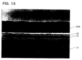
- FIG. 13 is a view showing an electron micrograph of a memory cell array according to an example of manufacturing steps of the fourth ferroelectric memory according to an embodiment of the present invention.
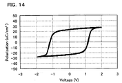
- FIG. 14 is a view showing hysteresis characteristics of a memory cell array according to an example of manufacturing steps of the fourth ferroelectric memory according to an embodiment of the present invention.
-
- (1) According to one embodiment of the present invention, there is provided a ferroelectric memory comprising:
- a substrate and a sheet-shaped device formed over the substrate through an
adhesive layer,
wherein the sheet-shaped device includes: - a memory cell array in which a ferroelectric layer is disposed at least in intersecting regions of a plurality of lower electrodes and a plurality of upper electrodes, the lower and upper electrodes being formed in the shape of lines; and
- a peripheral circuit section for the memory cell array. According to this ferroelectric memory, the memory cell array and the peripheral circuit section are planarly disposed as the sheet-shaped device. The sheet-shaped device is formed over the substrate through the adhesive layer, the substrate being different from a substrate on which the memory cell array and the peripheral circuit section are generally formed. Therefore, since a substrate having an arbitrary thickness or made of an arbitrary material can be selected, for example, the thickness of the entire device can be reduced or the device can be provided with flexibility. Therefore, this ferroelectric memory enables a ferroelectric memory having a novel thin structure to be realized.The "memory cell array" used herein refers to a structure in which memory cells are disposed in the shape of a matrix, the memory cells including a ferroelectric capacitor in which the ferroelectric layer is disposed in the intersecting regions of the lower electrodes and the upper electrodes, the lower and upper electrodes being formed in the shape of lines,.The "peripheral circuit" used herein includes at least a circuit for writing information in the memory cells and a circuit for reading information from the memory cells.The adhesive layer is not necessarily formed as a layer differing from the substrate, and may be integrally formed with the substrate. For example, in the case of bonding the substrate and the sheet-shaped device by using a property of a material of the substrate, a layer near the surface of the substrate is included in the adhesive layer.
- (2) According to another embodiment of the present invention, there is provided
a ferroelectric memory comprising:
- a plurality of laminates which include substrates and sheet-shaped devices
formed over the substrates through adhesive layers, respectively,
wherein the laminates are stacked, and
wherein each of the sheet-shaped devices includes: - a memory cell array in which a ferroelectric layer is disposed at least in intersecting regions of a plurality of lower electrodes and a plurality of upper electrodes, the lower and upper electrodes being formed in the shape of lines; and
- a peripheral circuit section for the memory cell array. This ferroelectric memory has a novel structure in which the thickness of the laminate including the substrate and the sheet-shaped device can be reduced. Therefore, the thickness of the entire device can be reduced or the degree of integration can be increased while providing the device with flexibility, for example.
- (3) According to a further embodiment of the present invention, there is
provided a ferroelectric memory comprising:
- a substrate and a plurality of sheet-shaped devices stacked over the substrate
through a plurality of adhesive layers,
wherein each of the sheet-shaped devices includes: - a memory cell array in which a ferroelectric layer is disposed at least in intersecting regions of a plurality of lower electrodes and a plurality of upper electrodes, the lower and upper electrodes being formed in the shape of lines; and
- a peripheral circuit section for the memory cell array. This ferroelectric memory has a structure in which a plurality of sheet-shaped devices are stacked through the adhesive layers. Therefore, the thickness of the entire device can be further reduced while stacking and integrating the sheet-shaped devices. Therefore, this ferroelectric memory has a novel structure, whereby the thickness of the entire device can be reduced or the degree of integration can be increased while providing the device with flexibility.The above ferroelectric memory may have any of the following features.
- (A) The above ferroelectric memory and a sheet-shaped operation processing device may be stacked. According to this feature, the degree of integration of an embedded device including a memory device having a novel thin structure and an operation processing device can be increased.
- (B) An insulating substrate having a through-hole may be disposed between the stacked sheet-shaped devices. According to this feature, since the stacked devices are electrically connected through the through-hole formed in the insulating substrate, a mounting area of the device can be reduced and the interconnect length can be reduced, whereby the device can be driven at high speed.
- (C) The insulating substrate may include an interconnect layer on at least one surface of the insulating substrate or inside the insulating substrate. According to this feature, since interconnection between the stacked devices or in each device is achieved through the insulating substrate, the interconnect structure of each device can be simplified.
- (4) According to still another embodiment of the present invention, there is
provided a method of manufacturing a ferroelectric memory comprising:
- forming a separation layer which changes in a property by absorbing light over a light transmissive first substrate;
- forming a memory cell array, in which a ferroelectric layer is disposed at least in intersecting regions of a plurality of lower electrodes and a plurality of upper electrodes over a predetermined portion of the separation layer, the lower and upper electrodes being formed in the shape of lines;
- forming a peripheral circuit section for the memory cell array over the separation layer in a portion other than the predetermined portion;
- bonding a sheet-shaped device including the memory cell array and the peripheral circuit section to a second substrate through at least an adhesive layer; and
- removing the sheet-shaped device from the first substrate by applying light to the separation layer through one surface of the first substrate. In this method of manufacturing a ferroelectric memory, the separation layer is formed on the light transmissive first substrate, and the memory cell array and the peripheral circuit section for the memory cell array are formed on the separation layer.The sheet-shaped device including the memory cell array and the peripheral circuit section is then bonded to the second substrate through the adhesive layer, and the sheet-shaped device is removed from the first substrate together with the second substrate at the separation layer by applying light to the separation layer from the back surface of the first substrate. The sheet-shaped device may be removed by changing the properties of the separation layer by applying light to the separation layer through the light transmissive first substrate. In this case, a material having a property absorbing applied light and causing separation inside the layer or on the surface by ablation may be used for the separation layer. There may be a case where gas is released from the separation layer by the application of light, whereby the separation effect is obtained.There are no specific limitations to the second substrate. The second substrate is selected in consideration of convenience of handling after removed from the first substrate.Therefore, according to this method of manufacturing a ferroelectric memory, a ferroelectric memory having a novel thin structure can be manufactured by removing the sheet-shaped device from the first substrate on which the sheet-shaped device is formed.This method of manufacturing a ferroelectric memory may have any of the following features.
- (D) The method of manufacturing a ferroelectric memory may further comprise stacking a plurality of laminates including the second substrate and the sheet-shaped device removed from the first substrate. According to this feature, since the sheet-shaped devices are stacked by stacking the laminates including the second substrate, handling capability during manufacturing steps is increased and the degree of integration of the ferroelectric memory can be increased by multi-layering with simplified steps.
- (E) The method of manufacturing a ferroelectric memory may further comprise:
- bonding the sheet-shaped device removed from the first substrate to another sheet-shaped device formed over another first substrate with a separation layer interposed in-between through an adhesive layer, and removing the other first substrate by applying light through one surface of the other first substrate,
- (5) According to a still further embodiment of the present invention, there is
provided a method of manufacturing a ferroelectric memory comprising:
- forming a separation layer which changes in a property by absorbing light over each of a light transmissive first substrate and a light transmissive second substrate;
- forming a memory cell array, in which a ferroelectric layer is disposed at least in intersecting regions of a plurality of lower electrodes and a plurality of upper electrodes over the separation layer formed over the first substrate, the lower and upper electrodes being formed in the shape of lines;
- forming a peripheral circuit section for the memory cell array over the separation layer formed over the second substrate;
- bonding the memory cell array and the peripheral circuit section to a third substrate through at least adhesive layers; and
- removing the memory cell array and the peripheral circuit section respectively from the first substrate and the second substrate by applying light to the separation layers through one surface of the first substrate and through one surface of the second substrate. According to this method of manufacturing a ferroelectric memory, the memory cell array is formed over the first substrate and the peripheral circuit section is formed over the second substrate. Specifically, a thin ferroelectric memory can be manufactured by forming the memory cell array and the peripheral circuit section on different substrates, bonding the memory cell array and the peripheral circuit section to the third substrate, and removing the original substrates.Therefore, according to this method of manufacturing a ferroelectric memory, since the memory cell array and the peripheral circuit section each of which has different manufacturing steps are formed over different substrates, efficiency of the entire manufacturing steps is improved. Moreover, since the memory cell array and the peripheral circuit section can be freely arranged over the third substrate, the degrees of freedom of the device design are increased.The method of manufacturing a ferroelectric memory may comprise stacking a plurality of laminates including the third substrate and a sheet-shaped device which includes the memory cell array and the peripheral circuit section respectively removed from the first substrate and the second substrate.According to this method of manufacturing a ferroelectric memory, the sheet-shaped devices are stacked by stacking the laminates including the third substrate. Therefore, according to this manufacturing method, the steps can be simplified due to the excellent handling capability of the laminates, and the degree of integration can be increased by multi-layering. Moreover, according to this manufacturing method, since a process which causes a large amount of load to each section of an element, such as a formation step of an interlayer dielectric, can be omitted when multi-layering the sheet-shaped devices, the sheet-shaped devices can be multi-layered and integrated while securing the characteristics of the sheet-shaped devices.
- (6) According to yet another embodiment of the present invention, there is
provided a method of manufacturing a ferroelectric memory comprising:
- forming a first laminate including a memory cell array, in which a ferroelectric layer is disposed at least in intersecting regions of a plurality of lower electrodes and a plurality of upper electrodes over a first substrate having a coefficient of thermal expansion smaller than a coefficient of thermal expansion of a ferroelectric material, the lower and upper electrodes being formed in the shape of lines;
- subjecting the first laminate to a first heat treatment and subsequent cooling to cause strain in the first laminate, and removing the memory cell array from the first substrate by subjecting the first laminate to a second heat treatment;
- forming a separation layer which changes in a property by absorbing light over a light transmissive second substrate, and forming a second laminate which includes a peripheral circuit for the memory cell array over the separation layer;
- bonding the second laminate on the side of the peripheral circuit to a third substrate;
- removing the peripheral circuit from the second substrate by changing the properties of the separation layer by applying light to the separation layer from the side of the second substrate of the second laminate; and
- bonding the memory cell array removed from the first substrate to the third substrate. In this method of manufacturing a ferroelectric memory, strain is generated in the first laminate by subjecting the first laminate to the first heat treatment and the subsequent cooling. The difference in the amount of expansion between the first substrate and the memory cell array including strain is increased in the second heat treatment, whereby the memory cell array is removed from the first substrate. The peripheral circuit is removed from the second laminate by applying light to the separation layer which changes in a property by the application of light.According to this manufacturing method, since the memory cell array can be formed while reducing the hydrogen generation process as much as possible, deterioration of the characteristics of the memory cell array can be reduced in comparison with the case of forming the memory cell array and the peripheral circuit continuously. Moreover, since stress based on the strain due to the thermal load can be reduced in the second heat treatment for removing the memory cell array, the memory cell array can be removed while eliminating the strain generated in the first heat treatment.In this method of manufacturing a ferroelectric memory, the first heat treatment may be performed at a temperature lower than a temperature at which strain is generated at least in the first substrate, andthe second heat treatment may be performed at a temperature equal to or lower than the temperature of the first heat treatment. This enables strain to be generated only in the memory cell array in the first laminate in the first heat treatment, whereby a difference in the amount of expansion between the memory cell array and the first substrate can be increased in the second heat treatment. Moreover, since a sufficient difference in the amount of expansion can be secured in the second heat treatment even at a temperature equal to or lower than the temperature of the first heat treatment, and load to the memory cell array can be reduced, deterioration of the characteristics due to the thermal load can be reduced. Preferred embodiments of the present invention are described below in more detail with reference to the drawings.
-
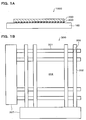
- FIG. 1A is a cross-sectional view schematically showing a first
ferroelectric memory 1000 according to an embodiment of the present invention. - In the first
ferroelectric memory 1000 according to the present embodiment, a sheet-shapeddevice 300 is formed on aflexible substrate 100 through anadhesive layer 200. - There are no specific limitations to the
flexible substrate 100. A substrate having flexibility may be selected in order to increase applicability of the firstferroelectric memory 1000. It is expected that the market for devices for which flexibility is required, such as an IC card, will expand in the future. Therefore, it is necessary to widen the application range in the field of ferroelectric memory by providing the ferroelectric memory with flexibility. As examples of theflexible substrate 100, a synthetic resin, a thin metal sheet, and the like can be given. In the case of selecting a substrate having no flexibility, a glass substrate or a semiconductor substrate may be used. - As examples of the
adhesive layer 200, various adhesives such as a reaction curable adhesive, a heat curable adhesive, and a photocurable adhesive such as a ultraviolet curable adhesive can be given. Theadhesive layer 200 may not be formed as a layer differing from theflexible substrate 100. Theadhesive layer 200 may be integrally formed with theflexible substrate 100. This applies to the case where the sheet-shapeddevice 300 is caused to adhere to theflexible substrate 100 by thermocompression bonding utilizing a surface property of theflexible substrate 100, for example. - As shown in FIG. 1B, the sheet-shaped
device 300 is formed by amemory cell array 304 and aperipheral circuit section 307 for thememory cell array 304 which are disposed in different regions on theflexible substrate 100. - In the
memory cell array 304,lower electrodes 301 andupper electrodes 302 which are formed in the shape of lines are disposed to intersect, and memory cells, in which a ferroelectric layer (not shown) is disposed in anintersecting region 303, are arranged in the shape of a matrix. - In the
memory cell array 304, thelower electrodes 301 function as word lines for selecting rows, and theupper electrodes 302 function as bit lines for selecting columns. Thelower electrodes 301 and theupper electrodes 302 may be formed so that thelower electrodes 301 function as the word lines and theupper electrodes 302 function as the bit lines. - The
peripheral circuit section 307 has at least a function of writing information in each memory cell of thememory cell array 304 and reading information from each memory cell. Theperipheral circuit section 307 includes a driver circuit and a signal detection circuit for selectively controlling thelower electrodes 301 and theupper electrodes 302 and the like. As specific examples of these circuits, a Y gate, sense amplifier, input/output buffer, X address decoder, Y address decoder, address buffer, and the like can be given. - The
peripheral circuit section 307 can be thinly formed by forming theperipheral circuit section 307 by using thin film transistors (TFTs) or other thin film semiconductor devices. - As described above, in the first
ferroelectric memory 1000 according to the present embodiment, thememory cell array 304 and theperipheral circuit section 307 are formed on theflexible substrate 100 through theadhesive layer 200 instead of a substrate on which thememory cell array 304 and theperipheral circuit section 307 are generally formed. Moreover, since theflexible substrate 100 having an arbitrary thickness or made of an arbitrary material can be selectively used, the thickness of the entire device can be reduced or the device can be provided with flexibility. - Therefore, the first
ferroelectric memory 1000 according to the present embodiment enables a novel thin ferroelectric memory structure to be realized. Moreover, since the firstferroelectric memory 1000 according to the present embodiment has high flexibility by employing a material having flexibility for theflexible substrate 100, the firstferroelectric memory 1000 can be applied for various uses such as an IC card. - A method of manufacturing the first
ferroelectric memory 1000 according to the present embodiment is described below. - FIGS. 2A to 2C are views schematically showing manufacturing steps of the first
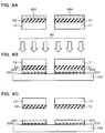
ferroelectric memory 1000 according to the present embodiment. - As shown in FIG. 2A, a
separation layer 20 is formed on aseparation substrate 10, and a sheet-shapeddevice 300 is formed on theseparation layer 20. - As a material for the
separation substrate 10, a material having a property of transmitting light such as laser light may be selected. For example, glass, a resin such as plastic, and the like can be given as such a material. - As a material for the
separation layer 20, a material which changes in properties by application of light such as laser light and can be fused, such as amorphous silicon, may be used. As the material for theseparation layer 20, various substances such as an oxide such as silicon oxide, ceramics, an organic polymer compound, or a metal may be used in addition to amorphous silicon. As such substances, substances disclosed in Japanese Patent Application Laid-open No. 11-74533 may be used. In the case of using an organic polymer compound as the material for theseparation layer 20, a polyolefin such as polyethylene and polypropylene, polyimide, polyamide, polyester, polymethylmethacrylate (PMMA), polyphenylene sulfide (PPS), polyether sulfone (PES), epoxy resin, or the like may be used. - In the present embodiment, the
memory cell array 304 included in the sheet-shapeddevice 300 is formed by forming thelower electrodes 301, the ferroelectric layer (not shown), and theupper electrodes 302 shown in FIG. 1B in that order. - As examples of an electrode material, Pt, Ir, IrOx, RuOx, SrRuOx, LaSrCoOx, and the like can be given. As the lower electrode and the upper electrode, a single layer or a laminate of a plurality of layers of the above electrode material may be used. The lower electrode and the upper electrode may be formed by using a conventional deposition method such as a sputtering method, a vapor deposition method, or a CVD method.
- As examples of a material for the ferroelectric layer, PZT (PbZrxTi1-xO3), SBT (SrBi2Ta2O9), a material in which a metal such as niobium, nickel, or magnesium is added to PZT or SBT, and the like can be given. The ferroelectric layer may be formed by using a conventional method such as a spin coating method or a dipping method using a sol-gel material or MOD (Metal Organic Decomposition) material, a sputtering method, an MOCVD method, or a laser ablation method.
- The
peripheral circuit section 307 shown in FIG. 1B may be formed by forming circuits using thin-film semiconductor devices such as TFTs by using a conventional semiconductor process, for example. - In the case of forming the
peripheral circuit section 307 by using thin-film semiconductor devices such as TFTs which can be formed by using a low-temperature process, the ferroelectric layer of thememory cell array 304 may be formed by crystallizing a mixture of a sol-gel material of a paraelectric including Si or Ge, such as Bi2SiOx, Bi2GeOx, Zr2SiOx, or Pb2SiOx, and a sol-gel material of a ferroelectric such as PZT or SBT as described above. According to this formation method, since the crystallization temperature can be decreased by allowing Si or Ge included in the material to function as a catalyst, thermal damage to theperipheral circuit section 307 can be reduced even in the case of forming thememory cell array 304 after forming theperipheral circuit section 307. - In the case of forming the ferroelectric layer by using a single substance such as PZT or SBT, crystal modification is induced by annealing the ferroelectric layer by applying laser light to the ferroelectric layer after deposition, whereby a ferroelectric layer having an excellent crystal structure can be formed. Such a formation method of the ferroelectric layer also enables thermal damage to the
peripheral circuit section 307 to be reduced even in the case of forming thememory cell array 304 after forming theperipheral circuit section 307. - As shown in FIG. 2B, the sheet-shaped
device 300 formed on theseparation substrate 10 through theseparation layer 20 is bonded to theflexible substrate 100 through theadhesive layer 200. As shown in FIG. 2C, the sheet-shapeddevice 300 is removed from theseparation substrate 10 together with theflexible substrate 100 to form theferroelectric memory 1000. - The sheet-shaped
device 300 may be removed by changing the properties of theseparation layer 20 by applying light such as laser light to theseparation layer 20 through theseparation substrate 10 which transmits light such as laser light, as shown in FIG. 2B. In this case, as a material for theseparation layer 20, a material having a property of absorbing the applied light such as laser light and causing separation inside the layer or on the surface by ablation. There may be a case where gas is released from theseparation layer 20 by the application of light such as laser light, whereby the separation effect is obtained. Specifically, there is a case where a component included in theseparation layer 20 is gasified and released, or a case where gas is released when theseparation layer 20 absorbs light to contribute to separation. For example, separation in theseparation layer 20 can be facilitated by mixing a substance which easily absorbs laser light (pigment, for example) or a substance which generates gas due to light such as laser light or absorption heat of light such as laser light with the material for theseparation layer 20. - As described above, in the method of manufacturing the first
ferroelectric memory 1000 according to the present embodiment, the firstferroelectric memory 1000 having a novel thin structure can be manufactured by removing the sheet-shapeddevice 300 from theseparation substrate 10 on which the sheet-shapeddevice 300 is formed. - FIG. 3A is a cross-sectional view schematically showing a
ferroelectric memory 1100 according to a first modification of the first ferroelectric memory of the present embodiment. In FIG. 3A, sections having substantially the same functions as the sections shown in FIGS. 1A and 1B are indicated by the same symbols. Detailed description of these sections is omitted. - As shown in FIG. 3A, in the
ferroelectric memory 1100 according to this example, thememory cell array 304 and theperipheral circuit section 307 are formed on theflexible substrate 100 throughadhesive layers - The
ferroelectric memory 1100 of this example differs from the firstferroelectric memory 1000 in that thememory cell array 304 and theperipheral circuit section 307 are separately mounted on theflexible substrate 100. Thememory cell array 304 is electrically connected with theperipheral circuit section 307 through aninterconnect layer 50. - An insulating
layer 40 is formed on the top and the periphery of thememory cell array 304 and theperipheral circuit section 307 in order to prevent occurrence of short circuits between thememory cell array 304 and theperipheral circuit section 307 when forming theinterconnect layer 50. However, the insulatinglayer 40 is not an indispensable constituent element. - The
ferroelectric memory 1100 of this example may be formed by the following manufacturing steps. - FIGS. 4A to 4C and 5A to 5C are views schematically showing the manufacturing steps of the
ferroelectric memory 1100. - As shown in FIG. 4A, a
separation layer 21 and thememory cell array 304 are formed on aseparation substrate 11, and aseparation layer 22 and theperipheral circuit section 307 are formed on aseparation substrate 12. Electrode pads (not shown) may be formed on thememory cell array 304 and theperipheral circuit section 307 in advance on the side of theseparation substrates - As shown in FIG. 4B, the
memory cell array 304 and theperipheral circuit section 307 are bonded to theflexible substrate 100 through theadhesive layers memory cell array 304 and theperipheral circuit section 307 are formed) of theseparation substrates memory cell array 304 and theperipheral circuit section 307 are respectively removed from theseparation substrates flexible substrate 100, as shown in FIG. 4C. - Then, the
memory cell array 304 is electrically connected with theperipheral circuit section 307 by forming interconnects according the manufacturing steps shown in FIGS. 5A to 5C. - The insulating
layer 40 is formed on the removedmemory cell array 304 andperipheral circuit section 307. The insulatinglayer 40 may be formed of an insulating inorganic material such as SiO2 or an insulating organic material such as polyimide, for example. In the case of using an insulating inorganic material, the insulatinglayer 40 may be deposited by using a sputtering method or a CVD method, for example. In the case of using an insulating organic material, the insulatinglayer 40 may be deposited by using a spin coating method, for example. - As shown in FIG. 5B, the electrode pads (not shown) of the
memory cell array 304 and theperipheral circuit section 307 are exposed by etching the insulatinglayer 40, for example. - The electrode pads of the
memory cell array 304 and theperipheral circuit section 307 are electrically connected through theinterconnect layer 50. Theinterconnect layer 50 may be deposited by using a metal such as aluminum, copper, or tungsten using a conventional method such as a sputtering method. - As described above, the
ferroelectric memory 1100 of the first modification also enables a novel thin ferroelectric memory structure to be realized in the same manner as the firstferroelectric memory 1000. Moreover, since theferroelectric memory 1100 of the first modification also has high flexibility by employing a material having flexibility as theflexible substrate 100, theferroelectric memory 1100 can be applied for various uses such as an IC card. - According to the method of manufacturing the
ferroelectric memory 1100, since thememory cell array 304 and theperipheral circuit section 307 for which the manufacturing steps differ are separately formed on theseparation substrates memory cell array 304 and theperipheral circuit section 307 on theflexible substrate 100 can be set without limitations, whereby the degrees of freedom of the device design are increased. - FIG. 3B is a cross-sectional view schematically showing a
ferroelectric memory 1200 according to a second modification of the first ferroelectric memory of the present embodiment. In FIG. 3B, sections having substantially the same functions as the sections shown in FIG. 3A are indicated by the same symbols. Detailed description of these sections is omitted. - The
ferroelectric memory 1200 of this example differs from theferroelectric memory 1100 of the first modification in that thememory cell array 304 is electrically connected with theperipheral circuit section 307 by using aninterconnect pattern 60 formed in theflexible substrate 100 and bumps 71 and 72. - The
ferroelectric memory 1200 may be manufactured by using the same manufacturing steps as the manufacturing steps of theferroelectric memory 1100 according to the first modification. However, thebumps interconnect pattern 60 formed in theflexible substrate 100 in the step shown in FIG. 4B. Thememory cell array 304 and theperipheral circuit section 307 are bonded to theflexible substrate 100 through theadhesive layers interconnect pattern 60 formed in theflexible substrate 100 may be connected with thememory cell array 304 and theperipheral circuit section 307 by thermal compression bonding of an anisotropic conductive film (ACF) or anisotropic conductive paste (ACP) instead of using thebumps - Since the
interconnect layer 50 is not formed in the manufacturing steps of theferroelectric memory 1200, it is unnecessary to perform the steps shown in FIG. 5B and 5C, whereby the manufacturing steps can be simplified. - As described above, the
ferroelectric memory 1200 according to the second modification also enables a novel and extremely thin ferroelectric memory structure to be realized in the same manner as the firstferroelectric memory 1000. Moreover, since theferroelectric memory 1200 of the second modification also has high flexibility by employing theflexible substrate 100 having flexibility, theferroelectric memory 1200 can be applied for various uses such as an IC card. - In the method of manufacturing the
ferroelectric memory 1200, since thememory cell array 304 and theperipheral circuit section 307 for which the manufacturing steps differ are separately formed on theseparation substrates memory cell array 304 and theperipheral circuit section 307 on theflexible substrate 100 can be set without limitations, the degrees of freedom of the device design are increased. - FIG. 6 is a cross-sectional view schematically showing a second
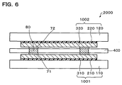
ferroelectric memory 2000 according to the present embodiment. In FIG. 6, sections having substantially the same functions as the sections shown in FIGS. 1A and 1B are indicated by the same symbols. Detailed description of these sections is omitted. - The second
ferroelectric memory 2000 has a structure in which laminates 1001 and 1002, in which sheet-shapeddevices flexible substrates adhesive layers substrate 400 including through-holes 80 are disposed between thelaminates - The
flexible substrates substrate 400 may be formed of a conventional material having an insulating property. For example, a material having flexibility such as a synthetic resin may be used. - The
laminates - The sheet-shaped
devices laminates holes 80 formed in the insulatingsubstrate 400 and thebumps holes 80. - The sheet-shaped
devices holes 80 formed in the insulatingsubstrate 400 by thermocompression bonding of an anisotropic conductive film (ACF) or anisotropic conductive paste (ACP) instead of using thebumps - An interconnect layer (not shown) may be formed inside the insulating
substrate 400 or on at least one surface of the insulatingsubstrate 400 in addition to the through-holes 80. In this case, this interconnect layer may be used as a part of interconnects inside the sheet-shapeddevices devices devices - According to the second
ferroelectric memory 2000, since the thicknesses or the materials for theflexible substrates laminates laminates flexible substrates substrate 400 by using a material having flexibility, applicability is increased. - Therefore, the second
ferroelectric memory 2000 enables a ferroelectric memory having a novel thin structure to be realized and the degree of integration to be increased. According to the secondferroelectric memory 2000, since the stacked sheet-shaped devices are electrically connected through the through-holes 80 formed in the insulatingsubstrate 400, the mounting area of the devices can be reduced. Moreover, since the interconnect length between the devices can be reduced, an increase in drive speed can be expected. - According to the method of manufacturing the second
ferroelectric memory 2000 according to the present embodiment, since the sheet-shapeddevices flexible substrates devices devices devices - As a modification of the second
ferroelectric memory 2000, aferroelectric memory 2100 shown in FIG. 7 can be given. - In the
ferroelectric memory 2100, thelaminates 1001 to 1003, in which the sheet-shapeddevices 310 to 330 are respectively formed on theflexible substrates 110 to 130 through theadhesive layers 210 to 230, are electrically connected through the through-holes flexible substrates bumps 71 to 74. - In the case of forming the
ferroelectric memory 2100, thebumps holes flexible substrates flexible substrates devices laminates holes devices flexible substrates devices adhesive layers ferroelectric memory 1000. - The
laminates 1001 to 1003 thus formed are connected through thebumps laminates laminates 1001 to 1003 and the connection inside thelaminates bumps 71 to 74. - In the
ferroelectric memory 2100 of this example, the thicknesses and the materials for theflexible substrates 110 to 130 may be arbitrarily selected in the same manner as the secondferroelectric memory 2000. Therefore, since the thicknesses of thelaminates 1001 to 1003 can be reduced, the thickness of the entire device can be reduced or the device can be provided with flexibility. Therefore, theferroelectric memory 2100 also enables a ferroelectric memory having a novel thin structure to be realized and the degree of integration to be increased. - In the present embodiment and its modification, a laminate (not shown) including a sheet-shaped operation processing device, such as a central processing unit (CPU), a micro processing unit (MPU), or a digital signal processor (DSP), formed by using thin film transistors may be further stacked by using the same method. According to this feature, an embedded device having a novel thin structure which includes a memory device and an operation processing device can be highly integrated.
- FIG. 8 is a cross-sectional view schematically showing a third
ferroelectric memory 2200 of the present embodiment. In FIG. 8, sections having substantially the same function as the sections described above are indicated by the same symbols. Detailed description of these sections is omitted. - The third
ferroelectric memory 2200 of the present embodiment is formed by stacking the sheet-shapeddevices 310 to 330 on theflexible substrate 100. The through-holes 81 to 83 are respectively formed in the sheet-shapeddevices 310 to 330. One end of each of the through-holes 81 to 83 is electrically connected through thebumps devices 310 to 330. Each of the through-holes 81 to 83 is electrically connected with predetermined areas of the sheet-shapeddevices 310 to 330. - The sheet-shaped
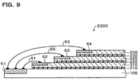
devices 310 to 330 may be electrically connected by using a feature of aferroelectric memory 2300 shown in FIG. 9, which is a modification of the present embodiment. - In the
ferroelectric memory 2300 of the modification shown in FIG. 9, the sheet-shapeddevices 310 to 330 are electrically connected by bondingelectrode pads 62 to 64 for external interconnection formed on each of the sheet-shapeddevices 310 to 330 toelectrode pads 61 formed on theflexible substrate 100 throughwires 91 to 93. - In the third
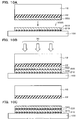
ferroelectric memory 2200 and theferroelectric memory 2300 in the modification, the sheet-shapeddevices 310 to 330 may be stacked on theflexible substrate 100 by using manufacturing steps shown in FIGS. 10A to 10C. - As shown in FIG. 10A, the first
ferroelectric memory 1000 manufactured by using the same method as described above, and the sheet-shapeddevice 320 formed on theseparation substrate 12 through theseparation layer 22 are provided. - As shown in FIG. 10B, the first
ferroelectric memory 1000 is bonded to the sheet-shapeddevice 320 through theadhesive layer 220, and thelaser light 30 is applied from the back surface of theseparation substrate 12, for example. The properties of theseparation layer 22 are changed by thelaser light 30 applied through theseparation substrate 12, whereby the sheet-shapeddevice 320 can be removed from theseparation substrate 12 in a state in which the sheet-shapeddevice 320 is bonded to the side of theflexible substrate 100, as shown in FIG. 10C. In the manufacture of the thirdferroelectric memory 2200 and theferroelectric memory 2300 of the modification, a plurality of sheet-shaped devices can be stacked by repeating these steps. - In the third
ferroelectric memory 2200 of the present embodiment, the sheet-shapeddevices bumps 71 on the ends of at least one of the through-holes devices devices adhesive layer 220 in the step shown in FIG. 10B. In theferroelectric memory 2300 of the modification of the present embodiment, theelectrode pads 62 to 64 of the sheet-shapeddevices 310 to 330 may be connected with theelectrode pads 61 of theflexible substrate 100 by wire bonding after completing the stacking steps of the sheet-shapeddevices 310 to 330. - In the third
ferroelectric memory 2200 of the present embodiment and theferroelectric memory 2300 of the modification, the sheet-shapeddevices 310 to 330 are stacked on theflexible substrate 100 through theadhesive layers 210 to 230. Since the thickness of each layer to be stacked is about several microns, the ferroelectric memory is extremely thin even in a state in which the layers are stacked. Therefore, according to the thirdferroelectric memory 2200 and theferroelectric memory 2300 of the modification, a ferroelectric memory which has a novel thin structure and can be highly integrated can be realized. Moreover, according to the thirdferroelectric memory 2200 and theferroelectric memory 2300 of the modification, since the material or the thickness of theflexible substrate 100 can be arbitrarily selected, the device can be provided with flexibility. - In the manufacturing methods according to the present embodiment and the modification, since a process which causes a large amount of load to be applied to each section of the device, such as a formation step of an interlayer dielectric or the like, can be omitted when multi-layering the sheet-shaped
devices 310 to 330, the sheet-shapeddevices 310 to 330 can be multi-layered and integrated while securing the characteristics of the sheet-shapeddevices 310 to 330. - In the present embodiment and the modification, a layer of a sheet-shaped operation processing device, such as a central processing unit (CPU), a micro processing unit (MPU), or a digital signal processor (DSP), formed by using thin film transistors may be further stacked by using the same method. According to this feature, an embedded device having a novel thin structure which includes a memory device and an operation processing device can be highly integrated.
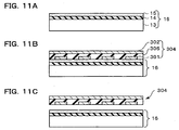
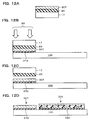
- FIGS. 11A to 11C and 12A to 12D are cross-sectional views schematically showing manufacturing steps of a fourth ferroelectric memory according to the present embodiment. In FIGS. 11A to 11C and 12A to 12D, sections having substantially the same function as the sections described above are indicated by the same symbols. Detailed description of these sections is omitted.
- The feature of the present embodiment is that the
memory cell array 304 is removed by using the difference in the amount of thermal expansion during a heat treatment. As shown in FIG. 11A, a substrate (first substrate) 16 for forming memory cells is provided. As thesubstrate 16 for forming memory cells, a substrate in which an SOI substrate in which asilicon oxide film 14 is formed on asilicon substrate 13 is covered with a TiOx film 15, which is suitable for forming a memory cell array, may be employed. Silicon has a temperature at which strain is generated due to heat (strain point) of about 1000°C. The strain point of silicon is higher than that of the ferroelectric material represented by PZT. The coefficient of thermal expansion of silicon is smaller than that of a generally used ferroelectric material. Therefore, the difference in the amount of thermal expansion between silicon and the memory cell array can be easily obtained. Specifically, thesubstrate 16 for forming memory cells is preferably formed of a material having at least a coefficient of thermal expansion smaller than that of the ferroelectric material. In the present embodiment, since a process which positively introduces strain into thememory cell array 304 is performed, thesubstrate 16 for forming memory cells is preferably formed of a material having a strain point higher than that of the ferroelectric material. - In the manufacturing method of the present embodiment, the
memory cell array 304 is formed by stacking thelower electrodes 301, theferroelectric layer 305, and theupper electrodes 302 in that order on thesubstrate 16 for forming memory cells, as shown in FIG. 11B. Thelower electrodes 301 and theupper electrodes 302 are in the shape of lines and formed to intersect. Thelower electrode 301, theupper electrode 302, and theferroelectric layer 305 disposed in the intersecting region of thelower electrode 301 and theupper electrode 302 function as a memory cell. Theferroelectric layer 305 is preferably formed of a material in which a paraelectric oxide containing silicon or germanium is added to PZT-type ferroelectric material as described above. - In the manufacturing method of the present embodiment, a laminate (first laminate) shown in FIG. 11B is subjected to a first heat treatment and subsequent cooling. The first heat treatment is performed at a temperature at which strain is not generated in the
substrate 16 for forming memory cells. Specifically, the first heat treatment is performed at a temperature which is lower than the strain point of the material for thesilicon substrate 13, which forms the greater part of thesubstrate 16 for forming memory cells, and is higher than the strain point of the material for theferroelectric layer 305 which makes up thememory cell array 304. - A second heat treatment is then performed in a state in which strain is generated in the
memory cell array 304. As a result, theferroelectric layer 305 of thememory cell array 304 is thermally expanded to a large extent in comparison with the state before the strain is introduced. This causes thememory cell array 304 to be removed from thesubstrate 16 for forming memory cells due to the difference in the amount of expansion between theferroelectric layer 305 and thesubstrate 16 for forming memory cells, as shown in FIG. 11C. Since the strain and stress of thememory cell array 304 which have bee generated during cooling after the first heat treatment are reduced during the second heat treatment, the characteristics of the removedmemory cell array 304 rarely deteriorate. - In the manufacturing method of the present embodiment, it is preferable that the first heat treatment be performed at a temperature lower than the temperature at which the strain is generated at least in the
substrate 16 for forming memory cells, and the second heat treatment be performed at a temperature equal to or lower than the temperature of the first heat treatment. This enables the strain to be preferentially generated in thememory cell array 304 during the first heat treatment, whereby the difference in the amount of expansion between thememory cell array 304 and thesubstrate 16 for forming memory cells can be increased during the second heat treatment. Moreover, the difference in the amount of expansion can be sufficiently secured during the second heat treatment even at a temperature equal to or lower than the temperature of the first heat treatment, if the strain can be preferentially generated in thememory cell array 304. Therefore, a load applied to thememory cell array 304 is reduced, whereby deterioration of the characteristics due to the thermal load can be reduced. - In the manufacturing method of the present embodiment, after removing the
memory cell array 304, theperipheral circuit 307 is formed according to the steps shown in FIGS. 12A to 12C, and thememory cell array 304 and theperipheral circuit 307 are bonded to thethird substrate 100, as shown in FIG. 12D. - As shown in FIG. 12A, the
peripheral circuit 307 for thememory cell array 304 is formed on a separation substrate (second substrate) 17 which can transmit light through theseparation layer 20 formed of a material which changes in properties by application of light. - As shown in FIG. 12B, a laminate (second laminate) formed of the
separation substrate 17, theseparation layer 20, and theperipheral circuit 307 is bonded to theflexible substrate 100 through theadhesive layer 210. The properties of theseparation layer 20 are changed by applying light (laser light, for example) to the laminate bonded to theflexible substrate 100 from the side of theseparation substrate 17 to remove theseparation substrate 17 from theperipheral circuit 307, as shown in FIG. 12C. - As shown in FIG. 12D, the
memory cell array 304 which is removed in the steps shown in FIGS. 11 A to 11C is bonded to theflexible substrate 100 through theadhesive layer 220. Thememory cell array 304 is electrically connected with theperipheral circuit 307 by forming interconnects and the like to obtain a ferroelectric memory. - Since the formation steps of the
peripheral circuit 307 can be separately performed from the formation steps of thememory cell array 304, these steps may be performed at the same time, or theperipheral circuit 307 may be formed before forming thememory cell array 304. - According to the manufacturing method of the present embodiment, since the
memory cell array 304 can be formed while reducing the hydrogen generation process as much as possible, deterioration of the characteristics of thememory cell array 304 can be prevented in comparison with the case of forming thememory cell array 304 and theperipheral circuit 307 continuously. Moreover, since the stress based on the strain introduced during the first heat treatment can be reduced by the second heat treatment for removing thememory cell array 304, thememory cell array 304 can be removed while eliminating the strain which has been generated. - An example of the method of manufacturing the fourth ferroelectric memory of the present embodiment is described below with reference to the drawings.
- In this example, the
memory cell array 304 including a Pt lower electrode, a PZTN ferroelectric layer, and a Pt upper electrode was formed on the substrate for forming a memory in which thesilicon substrate 13, thesilicon oxide film 14, and the TiOx film 15 were stacked, and removal of thememory cell array 304 was attempted. - The first heat treatment was performed at 400°C for 10 minutes in an N2 atmosphere, and the laminate was rapidly cooled on a stainless steel support. The laminate was heated to 400°C at a temperature increase rate of 10°C/min as the second heat treatment. As a result, it was confirmed that separation occurred between the
TiOx film 15 and thememory cell array 304 as shown in FIG. 13. It was confirmed that thememory cell array 304 can be removed by the second heat treatment at a temperature of about 150°C. - The reason therefor is considered to be as follows. Since silicon has a small coefficient of thermal expansion and a temperature at which strain is generated (strain point) as high as about 1000°C, which is higher than the strain point of the ferroelectric material such as PZT (about 400°C), strain was generated only in the
memory cell array 304 during the first heat treatment, and thememory cell array 304 containing the strain was abnormally expanded during the second heat treatment, whereby separation occurred at the surface of theTiOx film 15. - The hysteresis characteristics of the
memory cell array 304 thus removed were measured. As a result, a hysteresis loop having excellent squareness was obtained as shown in FIG. 14. According to the manufacturing method of the present embodiment, it was confirmed that thememory cell array 304 can be removed without causing the characteristics of thememory cell array 304 to deteriorate. - The preferred embodiments of the present invention are described above. However, the present invention is not limited to these embodiments. Various modifications and variations are possible within the scope of the present invention.
Claims (17)
- A ferroelectric memory comprising:wherein the sheet-shaped device includes:a substrate and a sheet-shaped device formed over the substrate through an adhesive layer,a memory cell array in which a ferroelectric layer is disposed at least in intersecting regions of a plurality of lower electrodes and a plurality of upper electrodes, the lower and upper electrodes being formed in the shape of lines; anda peripheral circuit section for the memory cell array.
- A ferroelectric memory comprising:wherein the laminates are stacked, anda plurality of laminates which include substrates and sheet-shaped devices formed over the substrates through adhesive layers, respectively,
wherein each of the sheet-shaped devices includes:a memory cell array in which a ferroelectric layer is disposed at least in intersecting regions of a plurality of lower electrodes and a plurality of upper electrodes, the lower and upper electrodes being formed in the shape of lines; anda peripheral circuit section for the memory cell array. - A ferroelectric memory comprising:wherein each of the sheet-shaped devices includes:a substrate and a plurality of sheet-shaped devices stacked over the substrate through a plurality of adhesive layers,a memory cell array in which a ferroelectric layer is disposed at least in intersecting regions of a plurality of lower electrodes and a plurality of upper electrodes, the lower and upper electrodes being formed in the shape of lines; anda peripheral circuit section for the memory cell array.
- A ferroelectric memory comprising:a sheet-shaped operation processing device; andthe ferroelectric memory as defined in any one of claims 1 to 3 stacked over the sheet-shaped operation processing device.
- The ferroelectric memory as defined in any one of claims 2 to 4,
wherein an insulating substrate having a through-hole is disposed between the stacked sheet-shaped devices. - The ferroelectric memory as defined in claim 5,
wherein the insulating substrate includes an interconnect layer on at least one surface of the insulating substrate or inside the insulating substrate. - A method of manufacturing a ferroelectric memory comprising:forming a separation layer which changes in a property by absorbing light over a light transmissive first substrate;forming a memory cell array, in which a ferroelectric layer is disposed at least in intersecting regions of a plurality of lower electrodes and a plurality of upper electrodes over a predetermined portion of the separation layer, the lower and upper electrodes being formed in the shape of lines;forming a peripheral circuit section for the memory cell array over the separation layer in a portion other than the predetermined portion;bonding a sheet-shaped device including the memory cell array and the peripheral circuit section to a second substrate through at least an adhesive layer; andremoving the sheet-shaped device from the first substrate by applying light to the separation layer through one surface of the first substrate.
- The method of manufacturing a ferroelectric memory as defined in claim 7, further comprising:stacking a plurality of laminates including the second substrate and the sheet-shaped device removed from the first substrate.
- The method of manufacturing a ferroelectric memory as defined in claim 7, further comprising:wherein a plurality of the sheet-shaped devices are stacked over the second substrate by performing this step at least once.bonding the sheet-shaped device removed from the first substrate to another sheet-shaped device formed over another first substrate with a separation layer interposed in-between through an adhesive layer, and removing the other first substrate by applying light through one surface of the other first substrate,
- A method of manufacturing a ferroelectric memory comprising:forming a separation layer which changes in a property by absorbing light over each of a light transmissive first substrate and a light transmissive second substrate;forming a memory cell array, in which a ferroelectric layer is disposed at least in intersecting regions of a plurality of lower electrodes and a plurality of upper electrodes over the separation layer formed over the first substrate, the lower and upper electrodes being formed in the shape of lines;forming a peripheral circuit section for the memory cell array over the separation layer formed over the second substrate;bonding the memory cell array and the peripheral circuit section to a third substrate through at least adhesive layers; andremoving the memory cell array and the peripheral circuit section respectively from the first substrate and the second substrate by applying light to the separation layers through one surface of the first substrate and through one surface of the second substrate.
- The method of manufacturing a ferroelectric memory as defined in claim 10, further comprising:stacking a plurality of laminates including the third substrate and a sheet-shaped device which includes the memory cell array removed from the first substrate and the peripheral circuit section removed from the second substrate.
- The method of manufacturing a ferroelectric memory as defined in any one of claims 7 to 11,
wherein a raw material for the ferroelectric layer of the memory cell array is a mixture of a ferroelectric material and a paraelectric material, and
wherein the ferroelectric layer is formed by crystallizing the mixture. - The method of manufacturing a ferroelectric memory as defined in claim 12, further comprising:annealing the ferroelectric layer after crystallization by applying laser light to the ferroelectric layer.
- A method of manufacturing a ferroelectric memory comprising:forming a first laminate including a memory cell array, in which a ferroelectric layer is disposed at least in intersecting regions of a plurality of lower electrodes and a plurality of upper electrodes over a first substrate having a coefficient of thermal expansion smaller than a coefficient of thermal expansion of a ferroelectric material, the lower and upper electrodes being formed in the shape of lines;subjecting the first laminate to a first heat treatment and subsequent cooling to cause strain in the first laminate, and removing the memory cell array from the first substrate by subjecting the first laminate to a second heat treatment;forming a separation layer which changes in a property by absorbing light over a light transmissive second substrate, and forming a second laminate which includes a peripheral circuit for the memory cell array over the separation layer;bonding the second laminate on the side of the peripheral circuit to a third substrate;removing the peripheral circuit from the second substrate by changing the properties of the separation layer by applying light to the separation layer from the side of the second substrate of the second laminate; andbonding the memory cell array removed from the first substrate to the third substrate.
- The method of manufacturing a ferroelectric memory as defined in claim 14,
wherein the first heat treatment is performed at a temperature lower than a temperature at which strain is generated at least in the first substrate, and
wherein the second heat treatment is performed at a temperature equal to or lower than the temperature of the first heat treatment. - The method of manufacturing a ferroelectric memory as defined in claim 14 or 15,
wherein a paraelectric phase including Si or Ge is mixed in the ferroelectric layer. - The method of manufacturing a ferroelectric memory as defined in any one of claims 14 to 16,
wherein the first substrate includes a silicon substrate.
Applications Claiming Priority (3)
| Application Number | Priority Date | Filing Date | Title |
|---|---|---|---|
| JP2002238014 | 2002-08-19 | ||
| JP2002238014 | 2002-08-19 | ||
| PCT/JP2003/010306 WO2004017410A1 (en) | 2002-08-19 | 2003-08-13 | Ferroelectric memory and its manufacturing method |
Publications (2)
| Publication Number | Publication Date |
|---|---|
| EP1548833A1 true EP1548833A1 (en) | 2005-06-29 |
| EP1548833A4 EP1548833A4 (en) | 2007-03-21 |
Family
ID=31884449
Family Applications (1)
| Application Number | Title | Priority Date | Filing Date |
|---|---|---|---|
| EP03788099A Withdrawn EP1548833A4 (en) | 2002-08-19 | 2003-08-13 | Ferroelectric memory and its manufacturing method |
Country Status (4)
| Country | Link |
|---|---|
| US (2) | US6917063B2 (en) |
| EP (1) | EP1548833A4 (en) |
| JP (1) | JPWO2004017410A1 (en) |
| WO (1) | WO2004017410A1 (en) |
Cited By (1)
| Publication number | Priority date | Publication date | Assignee | Title |
|---|---|---|---|---|
| EP1946374A1 (en) * | 2005-11-09 | 2008-07-23 | Semiconductor Energy Laboratory Co., Ltd. | Semiconductor device and manufacturing method thereof |
Families Citing this family (10)
| Publication number | Priority date | Publication date | Assignee | Title |
|---|---|---|---|---|
| JP2004241632A (en) * | 2003-02-06 | 2004-08-26 | Seiko Epson Corp | Ferroelectric memory and its manufacturing method |
| US7057877B2 (en) * | 2003-08-27 | 2006-06-06 | Seiko Epson Corporation | Capacitor, method of manufacture thereof and semiconductor device |
| JP2005136071A (en) * | 2003-10-29 | 2005-05-26 | Seiko Epson Corp | Cross point type ferroelectric memory |
| JP4653426B2 (en) | 2004-06-25 | 2011-03-16 | セイコーエプソン株式会社 | Semiconductor device |
| NO20052904L (en) * | 2005-06-14 | 2006-12-15 | Thin Film Electronics Asa | A non-volatile electrical memory system |
| JP4433200B2 (en) * | 2005-12-20 | 2010-03-17 | セイコーエプソン株式会社 | Ferroelectric capacitor and semiconductor device |
| KR20090103113A (en) * | 2008-03-27 | 2009-10-01 | 삼성전자주식회사 | Semiconductor device and method of manufacturing the same |
| US8455936B2 (en) * | 2010-02-25 | 2013-06-04 | Avago Technologies General Ip (Singapore) Pte. Ltd. | Configurable memory sheet and package assembly |
| US8987787B2 (en) * | 2012-04-10 | 2015-03-24 | Macronix International Co., Ltd. | Semiconductor structure and method for manufacturing the same |
| JP6381004B2 (en) * | 2014-03-27 | 2018-08-29 | インテル・コーポレーション | Process integration of multi-device flexible electronics system on chip (SOC) |
Citations (5)
| Publication number | Priority date | Publication date | Assignee | Title |
|---|---|---|---|---|
| DE3922423A1 (en) * | 1988-07-08 | 1990-01-11 | Olympus Optical Co | FERROELECTRIC MEMORY, AND METHOD FOR DRIVING AND PRODUCING SUCH A |
| WO2000038234A1 (en) * | 1998-12-04 | 2000-06-29 | Thin Film Electronics Asa | Scalable data processing apparatus |
| EP1017100A1 (en) * | 1998-03-02 | 2000-07-05 | Seiko Epson Corporation | Three-dimensional device |
| US6140009A (en) * | 1999-01-15 | 2000-10-31 | 3M Innovative Properties Company | Thermal transfer element for forming multilayer devices |
| US6249014B1 (en) * | 1998-10-01 | 2001-06-19 | Ramtron International Corporation | Hydrogen barrier encapsulation techniques for the control of hydrogen induced degradation of ferroelectric capacitors in conjunction with multilevel metal processing for non-volatile integrated circuit memory devices |
Family Cites Families (7)
| Publication number | Priority date | Publication date | Assignee | Title |
|---|---|---|---|---|
| JPH07202052A (en) * | 1993-12-28 | 1995-08-04 | Hitachi Ltd | Manufacture of semiconductor integrated circuit device |
| JP3809712B2 (en) | 1996-08-27 | 2006-08-16 | セイコーエプソン株式会社 | Thin film device transfer method |
| JP3690135B2 (en) * | 1998-09-10 | 2005-08-31 | セイコーエプソン株式会社 | Device manufacturing method |
| JP3620041B2 (en) * | 1999-12-09 | 2005-02-16 | セイコーエプソン株式会社 | MEMORY DEVICE, ITS MANUFACTURING METHOD, AND ELECTRONIC DEVICE |
| JP2002026282A (en) * | 2000-06-30 | 2002-01-25 | Seiko Epson Corp | Method of manufacturing simple matrix type memory element |
| JP2002269972A (en) * | 2000-12-27 | 2002-09-20 | Seiko Epson Corp | Semiconductor memory, and operating method for memory cell consisting of ferroelectric capacitors |
| JP2002217391A (en) * | 2001-01-23 | 2002-08-02 | Seiko Epson Corp | Method for manufacturing laminate and semiconductor device |
-
2003
- 2003-08-13 EP EP03788099A patent/EP1548833A4/en not_active Withdrawn
- 2003-08-13 WO PCT/JP2003/010306 patent/WO2004017410A1/en active Application Filing
- 2003-08-13 JP JP2004528873A patent/JPWO2004017410A1/en not_active Withdrawn
- 2003-08-14 US US10/640,264 patent/US6917063B2/en not_active Expired - Fee Related
-
2005
- 2005-06-08 US US11/147,279 patent/US20050263809A1/en not_active Abandoned
Patent Citations (5)
| Publication number | Priority date | Publication date | Assignee | Title |
|---|---|---|---|---|
| DE3922423A1 (en) * | 1988-07-08 | 1990-01-11 | Olympus Optical Co | FERROELECTRIC MEMORY, AND METHOD FOR DRIVING AND PRODUCING SUCH A |
| EP1017100A1 (en) * | 1998-03-02 | 2000-07-05 | Seiko Epson Corporation | Three-dimensional device |
| US6249014B1 (en) * | 1998-10-01 | 2001-06-19 | Ramtron International Corporation | Hydrogen barrier encapsulation techniques for the control of hydrogen induced degradation of ferroelectric capacitors in conjunction with multilevel metal processing for non-volatile integrated circuit memory devices |
| WO2000038234A1 (en) * | 1998-12-04 | 2000-06-29 | Thin Film Electronics Asa | Scalable data processing apparatus |
| US6140009A (en) * | 1999-01-15 | 2000-10-31 | 3M Innovative Properties Company | Thermal transfer element for forming multilayer devices |
Non-Patent Citations (1)
| Title |
|---|
| See also references of WO2004017410A1 * |
Cited By (2)
| Publication number | Priority date | Publication date | Assignee | Title |
|---|---|---|---|---|
| EP1946374A1 (en) * | 2005-11-09 | 2008-07-23 | Semiconductor Energy Laboratory Co., Ltd. | Semiconductor device and manufacturing method thereof |
| EP1946374A4 (en) * | 2005-11-09 | 2014-01-01 | Semiconductor Energy Lab | Semiconductor device and manufacturing method thereof |
Also Published As
| Publication number | Publication date |
|---|---|
| US6917063B2 (en) | 2005-07-12 |
| JPWO2004017410A1 (en) | 2005-12-08 |
| WO2004017410A1 (en) | 2004-02-26 |
| US20050263809A1 (en) | 2005-12-01 |
| EP1548833A4 (en) | 2007-03-21 |
| US20040232458A1 (en) | 2004-11-25 |
Similar Documents
| Publication | Publication Date | Title |
|---|---|---|
| US20050263809A1 (en) | Ferroelectric memory and method of fabricating the same | |
| US10672821B2 (en) | Sensor device and manufacturing method thereof | |
| JP4063082B2 (en) | Flexible electronic device and manufacturing method thereof | |
| JP4042182B2 (en) | IC card manufacturing method and thin film integrated circuit device manufacturing method | |
| CN100474629C (en) | Wireless chip and method of manufacturing the same | |
| US6814832B2 (en) | Method for transferring element, method for producing element, integrated circuit, circuit board, electro-optical device, IC card, and electronic appliance | |
| CN101024481B (en) | Micro electro mechanical system, semiconductor device, and manufacturing method thereof | |
| JP2005311205A (en) | Semiconductor device | |
| JP4103421B2 (en) | Electronic device and electronic equipment | |
| KR20090083362A (en) | Semiconductor device and manufacturing method thereof | |
| JPH11251518A (en) | Three-dimensional device | |
| JP2004172478A (en) | Semiconductor device, its manufacturing method, and measuring jig related to the semiconductor device | |
| JP2002217391A (en) | Method for manufacturing laminate and semiconductor device | |
| US7674634B2 (en) | Method of producing semiconductor device | |
| JP2001127259A (en) | Manufacturing method for non-volatile memory element | |
| JP2004296681A (en) | Ferroelectric film, forming method thereof, ferroelectric capacitor, manufacturing method thereof, and ferroelectric memory | |
| US20050013161A1 (en) | Ferroelectric memory and method of manufacturing the same | |
| JP5419139B2 (en) | Semiconductor integrated device and manufacturing method thereof | |
| JP2006245185A (en) | Organic ferroelectric memory and its fabrication process | |
| CN1312744C (en) | Method for manufacturing sull and strong dielectrics film and strong dielectrics components | |
| JP2006253295A (en) | Organic ferroelectric memory and its fabrication process | |
| JP5245029B2 (en) | Semiconductor device | |
| JP2001036025A (en) | Manufacture of ferroelectric memory device | |
| JP2006245184A (en) | Organic ferroelectric memory and its fabrication process | |
| JP4869808B2 (en) | Manufacturing method of semiconductor device |
Legal Events
| Date | Code | Title | Description |
|---|---|---|---|
| PUAI | Public reference made under article 153(3) epc to a published international application that has entered the european phase |
Free format text: ORIGINAL CODE: 0009012 |
|
| 17P | Request for examination filed |
Effective date: 20050207 |
|
| AK | Designated contracting states |
Kind code of ref document: A1 Designated state(s): AT BE BG CH CY CZ DE DK EE ES FI FR GB GR HU IE IT LI LU MC NL PT RO SE SI SK TR |
|
| AX | Request for extension of the european patent |
Extension state: AL LT LV MK |
|
| DAX | Request for extension of the european patent (deleted) | ||
| RBV | Designated contracting states (corrected) |
Designated state(s): DE GB |
|
| A4 | Supplementary search report drawn up and despatched |
Effective date: 20070215 |
|
| RIC1 | Information provided on ipc code assigned before grant |
Ipc: H01L 27/115 20060101ALN20070209BHEP Ipc: H01L 27/105 20060101ALN20070209BHEP Ipc: H01L 27/12 20060101ALI20070209BHEP Ipc: H01L 21/84 20060101ALI20070209BHEP Ipc: H01L 21/68 20060101ALI20070209BHEP Ipc: H01L 21/98 20060101ALI20070209BHEP Ipc: H01L 23/48 20060101ALI20070209BHEP Ipc: H01L 25/065 20060101AFI20070209BHEP |
|
| 17Q | First examination report despatched |
Effective date: 20070503 |
|
| STAA | Information on the status of an ep patent application or granted ep patent |
Free format text: STATUS: THE APPLICATION IS DEEMED TO BE WITHDRAWN |
|
| 18D | Application deemed to be withdrawn |
Effective date: 20090526 |