EP1554010B1 - Multi-mode crystal oscillator system selectively configurable to minimize power consumption or noise generation - Google Patents
Multi-mode crystal oscillator system selectively configurable to minimize power consumption or noise generation Download PDFInfo
- Publication number
- EP1554010B1 EP1554010B1 EP03773172A EP03773172A EP1554010B1 EP 1554010 B1 EP1554010 B1 EP 1554010B1 EP 03773172 A EP03773172 A EP 03773172A EP 03773172 A EP03773172 A EP 03773172A EP 1554010 B1 EP1554010 B1 EP 1554010B1
- Authority
- EP
- European Patent Office
- Prior art keywords
- crystal oscillator
- power supply
- frequency
- voltage
- series
- Prior art date
- Legal status (The legal status is an assumption and is not a legal conclusion. Google has not performed a legal analysis and makes no representation as to the accuracy of the status listed.)
- Expired - Lifetime
Links
- 239000013078 crystal Substances 0.000 title claims description 95
- 238000004891 communication Methods 0.000 claims description 42
- 239000003990 capacitor Substances 0.000 claims description 32
- 230000007423 decrease Effects 0.000 claims description 7
- 238000005259 measurement Methods 0.000 claims description 7
- 238000000034 method Methods 0.000 claims description 6
- 230000008878 coupling Effects 0.000 claims description 4
- 238000010168 coupling process Methods 0.000 claims description 4
- 238000005859 coupling reaction Methods 0.000 claims description 4
- 230000004044 response Effects 0.000 claims description 2
- 238000010586 diagram Methods 0.000 description 9
- 230000010355 oscillation Effects 0.000 description 4
- 239000004065 semiconductor Substances 0.000 description 3
- 238000012163 sequencing technique Methods 0.000 description 3
- 230000002457 bidirectional effect Effects 0.000 description 2
- 230000005540 biological transmission Effects 0.000 description 2
- 230000003247 decreasing effect Effects 0.000 description 2
- 230000002411 adverse Effects 0.000 description 1
- 230000008859 change Effects 0.000 description 1
- 230000000295 complement effect Effects 0.000 description 1
- 230000001351 cycling effect Effects 0.000 description 1
- 238000007599 discharging Methods 0.000 description 1
- 230000000694 effects Effects 0.000 description 1
- 230000005669 field effect Effects 0.000 description 1
- 235000003642 hunger Nutrition 0.000 description 1
- 238000002513 implantation Methods 0.000 description 1
- 238000009413 insulation Methods 0.000 description 1
- 238000012986 modification Methods 0.000 description 1
- 230000004048 modification Effects 0.000 description 1
- 238000012544 monitoring process Methods 0.000 description 1
- 230000003071 parasitic effect Effects 0.000 description 1
- 238000012545 processing Methods 0.000 description 1
- 239000007787 solid Substances 0.000 description 1
- 230000000638 stimulation Effects 0.000 description 1
- 239000000758 substrate Substances 0.000 description 1
- 230000002123 temporal effect Effects 0.000 description 1
Images


Classifications
-
- H—ELECTRICITY
- H03—ELECTRONIC CIRCUITRY
- H03L—AUTOMATIC CONTROL, STARTING, SYNCHRONISATION, OR STABILISATION OF GENERATORS OF ELECTRONIC OSCILLATIONS OR PULSES
- H03L7/00—Automatic control of frequency or phase; Synchronisation
-
- Y—GENERAL TAGGING OF NEW TECHNOLOGICAL DEVELOPMENTS; GENERAL TAGGING OF CROSS-SECTIONAL TECHNOLOGIES SPANNING OVER SEVERAL SECTIONS OF THE IPC; TECHNICAL SUBJECTS COVERED BY FORMER USPC CROSS-REFERENCE ART COLLECTIONS [XRACs] AND DIGESTS
- Y10—TECHNICAL SUBJECTS COVERED BY FORMER USPC
- Y10S—TECHNICAL SUBJECTS COVERED BY FORMER USPC CROSS-REFERENCE ART COLLECTIONS [XRACs] AND DIGESTS
- Y10S323/00—Electricity: power supply or regulation systems
- Y10S323/911—Medical electronics
Definitions
- the present invention is generally directed to crystal oscillators and in particular to the use of crystal oscillators in applications that require low power consumption, e.g., a battery-powered implantable medical device, and applications that require low noise, e.g., communication systems, and systems for selectively achieving both low power consumption and low noise generation.
- low power consumption e.g., a battery-powered implantable medical device
- low noise e.g., communication systems, and systems for selectively achieving both low power consumption and low noise generation.
- the present invention relates to systems and in particular communication systems which require the use of a crystal oscillator for controlling communication rates and/or modulation.
- the crystal oscillator and/or a power supply for the crystal oscillator must have any noise generation be minimized to thus maximize the signal-to-noise ratio for the transmitted signal and to maximize the capability to detect and demodulate a low signal-to-noise level receive signal.
- a communication system resides in a battery-powered system, it additionally becomes desirable to minimize power consumption whenever possible.
- the battery-powered system is implantable and miniaturized, the need to minimize power consumption is further exacerbated.
- 6,164,284 entitled “System of Implantable Devices For Monitoring and/or Affecting Body Parameters” and U.S. Patent No. 6,185,452 entitled “Battery Powered Patient Implantable Device” describe devices configured for implantation within a patient's body, i.e., beneath a patient's skin, for performing various functions including: (1) stimulation of body tissue and/or sensing of body parameters, and (2) communicating between implanted slave devices and a master device which may be external to a patient's body.
- implantable devices are preferably powered from rechargeable batteries.
- the time between rechargings is potentially limited. Accordingly, power conservation techniques to extend the battery life of such devices are particularly desirable.
- the present invention is thus directed to a multi-mode crystal oscillator system selectively configurable to minimize power consumption or noise generation to thus achieve desired battery life and communication performances suitable for such an implantable device.
- JP59168704 discloses a semiconductor integrated circuit the purpose of which is to attain low power consumption and to decrease oscillation start time by using in common an oscillating circuit of a complementary insulation gate field effect semiconductor integrated circuit and a substrate bias circuit.
- JP61195388 discloses a timepiece device to deal with supply interruption by a charging type battery of a small capacity by alternatively and switchingly using a high precision oscillator operating by current supply from the battery.
- the present invention is directed to a multi-mode crystal oscillator system selectively configurable to minimize power consumption or noise generation.
- a system is particularly applicable to the communication system of an implantable device, e.g., the microstimulator/sensor device described in U.S. Patent Nos. 6,164,284 ; 6,185,452 ; 6,472,991 ; and the like.
- their small size an axial dimension of less than 60 mm and a lateral dimension of less than 6 mm limits the size of the battery contained within and thus makes it essential to minimize power consumption. Additionally, the small size and battery capacity result in a limited amount of transmission power.
- embodiments of the present invention alternatively supply power to a crystal oscillator in either a first mode that minimizes power consumption or a second mode that minimizes noise generation.
- a crystal oscillator system configured for alternatively minimizing power consumption or noise generation, comprises: (1) a crystal oscillator; (2) a first power supply for powering the crystal oscillator in a first mode of operation, wherein the first power supply operates as a switching downconverter to minimize power consumption; (3) a second power supply for powering the crystal oscillator in a second mode of operation, wherein the second power supply operates as a series downconverter to minimize noise generation; and (4) mode switching circuitry for alternatively powering the crystal oscillator from the first or the second power supply according to desired system parameters.
- the crystal oscillator system is of particular value when used in a communication system operating according to a communication protocol wherein the communication protocol is configured to have a majority of its time dedicated to intermessage delay portions between transmit and/or receive message portions (see, for example, U.S. Patent No. 6,472,991 ) and whereby the mode switching circuitry selects the second mode of operation during the transmit and/or receive message portions and the mode switching circuitry selects the first mode of operation during the intermessage delay portions.
- the crystal oscillator additionally includes circuitry for adjusting the operating frequency of the crystal oscillator. In a preferred implementation, this adjustment is accomplished by coupling a programmable capacitance to at least one node of the crystal of the crystal oscillator.
- the present invention is directed to a multi-mode crystal oscillator system selectively configurable to minimize power consumption or noise generation.
- a system is particularly applicable to the communication system of an implantable device, e.g., the microstimulator/sensor device described in U.S. Patent Nos. 6,164,284 ; 6,185,452 ; 6,472,991 ; and the like.
- their small size an axial dimension of less than 60 mm and a lateral dimension of less than 6 mm limits the size of the battery contained within and thus makes it essential to minimize power consumption. Additionally, the small size and battery capacity result in a limited amount of transmission power.
- embodiments of the present invention alternatively supply power to a crystal oscillator in either a first mode that minimizes power consumption or a second mode that minimizes noise generation.
- a crystal oscillator system configured for alternatively minimizing power consumption or noise generation, comprises: (1) a crystal oscillator; (2) a first power supply for powering the crystal oscillator in a first mode of operation, wherein the first power supply operates as a switching downconverter to minimize power consumption; (3) a second power supply for powering the crystal oscillator in a second mode of operation, wherein the second power supply operates as a series downconverter to minimize noise generation; and (4) mode switching circuitry for alternatively powering the crystal oscillator from the first or the second power supply according to desired system parameters.
- the crystal oscillator system is of particular use when used in a communication system operating according to a communication protocol wherein the communication protocol is configured to have a majority of its frame time dedicated to intermessage delay portions between transmit and/or receive message portions and whereby the mode switching circuitry selects the second mode of operation during the transmit and/or receive message portions and the mode switching circuitry selects the first mode of operation during the intermessage delay portions.
- a communication protocol suitable for use with the present invention is described in commonly-owned U.S. Patent No. 6,472,991 (hereinafter referred to as the 991 patent), entitled “Multichannel Communication Protocol Configured To Extend The Battery Life Of An Implantable Device", the contents of which are incorporated herein by reference in their entirety.
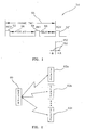
- FIG. 1 is a simplified timing diagram of such an exemplary bidirectional, half-duplex communication protocol 50 having temporally displaced receive 52 and transmit 54 time periods within each frame time 55.
- these relatively small receive 52 and transmit 54 time periods are separated by a relatively large intermessage delay time periods 56, 58.
- a master controller 60 (see FIG. 2 ) periodically sends command/status requests to one or more slaves 62a-62n (see FIG. 2 ) during receive period 52.
- Each slave 62 then transmits status/data information back to the master controller 60 during a transmit period 54 where the temporal position of transmit period 54 is defined at least in part by a unique identifier, e.g., a device ID, for each slave 62.
- a unique identifier e.g., a device ID
- the timing capability of each slave 62 must be sufficiently precise so that the transmit period 54 for each slave 62 will not overlap or otherwise interfere with another slave 62.
- the '991 patent teaches that power savings can be achieved by turning off portions of the communication circuitry when they are not needed, e.g., during the intermessage delay portions 56, 58. These power savings can be quite significant due to the relatively small percentage of the frame time 55 that receive and transmit circuitry portions are needed (see time periods 52, 54) versus the intermessage delay portions (see time periods 56, 58).
- a crystal oscillator is needed and since timing related to the crystal oscillator is used for determining the position of each time period, it must be operational throughout each cycle of the communication protocol 50. Accordingly, it is preferred that the selected crystal oscillator circuit consume relatively small amounts of power. Furthermore, it is preferred that the selected crystal oscillator circuit operate at a low voltage, e.g., preferably below 2 volts (0.9 volts in a preferred implementation). Such a crystal oscillator is described by Eric A. Vittoz, Marc G. R.
- Such a crystal oscillator (referred to herein as a Vittoz-type oscillator) reduces power by starving out the current needs of its FET circuitry to just above its critical needs during oscillation while providing an initial current startup burst to begin its oscillation.
- Embodiments of the present invention further reduce the power consumption of the selected oscillator, e.g., a Vittoz-type oscillator, by using a switching mode type of power supply to downconvert a power source to the operating voltage for the oscillator. Additionally, since such a switching mode power supply typically generates noise that could adversely effect communication capabilities, embodiments of the present invention switch to using a series downconverter mode power supply during the transmit 54 and/or receive 52 time periods.
- a switching mode type of power supply typically generates noise that could adversely effect communication capabilities
- FIG. 3 comprises a block diagram of an oscillator system 100 of the present invention wherein an oscillator 102, preferably a low power oscillator such as a Vittoz-type oscillator, is powered from at least two power supplies, a first one 104 that minimizes power consumption that is used during the intermessage delay portions 56, 58 and a second one 106 that minimizes noise generation that is used during the transmit 54 and/or receive 52 message portions.
- an oscillator 102 preferably a low power oscillator such as a Vittoz-type oscillator
- Oscillator 102 preferably runs off of a low voltage V o , e.g., 0.9 volts in a currently preferred implementation, and a low current, typically less than 50 ⁇ a and preferably less than 5 ⁇ a depending upon the programmed amplitude of oscillation to generate a frequency output f out , e.g., 25 MHz, suitable for division to obtain timing and modulation frequencies.
- V o low voltage
- a low current typically less than 50 ⁇ a and preferably less than 5 ⁇ a depending upon the programmed amplitude of oscillation to generate a frequency output f out , e.g., 25 MHz, suitable for division to obtain timing and modulation frequencies.
- Series downconverter mode power supply 106 operates in a conventional manner, e.g., in a constant voltage or current mode, to reduce the voltage V IN , e.g., 1.8 volts in a currently preferred implementation, to V o while switching downconverter mode power supply 104 operates on voltage V' IN , e.g., 2.7 volts in a currently preferred implementation, to reduce It to V o .
- Communication controller 108 operates upon communication signal 110 to retrieve status requests and control data and generates responsive signals 112.
- the communication controller 108 determines that it is processing the intermessage delay portions 56, 58, it activates the enable switching control line 114 to turn on the switching downconverter 104. Conversely, the enable series control line 116 is activated to turn on the series downconverter 106 during the receive 52 and/or transmit 54 time periods.
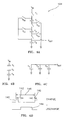
- FIG. 4A shows a simplified example of switching downconverter 104, suitable for use with the system 100 of FIG. 3 , which comprises a plurality of capacitors (C 1 -C 3 ) and switches (S 1 -S 3 , S 10 -S 13 ) for reconfiguring the charge and discharge paths to and from the capacitors to thus form a power efficient downconverter. While such a downconverter 104 is relatively power efficient as compared to the series downconverter 106, switching downconverter 104 does generate more noise (which is not desirable during receive 52 and/or transmit 54 time periods).
- an average current drain will be: time periods 56 + 58 / time periods 52 + 54 + 56 + 58 * 2.5 + time periods 52 + 54 / time periods 52 + 54 + 54 + 58 * peak current drain
- FIG. 4D a charging time period 140, capacitors C 1 , C 2 , C 3 are charged in series such that each one is charged to a voltage of one third of V IN .
- S 1 , S 2 , and S 3 are enabled while all of the other switches are disabled.
- FIG. 4B shows the configuration of the capacitors of FIG. 4A when the capacitors are being charged.
- all switches are disabled during a first inter-switching delay period 142 and then during a second time period, a discharging time period 144, switches S 1 -S 3 are disabled and the remaining switches S 10 -S 13 are enabled in order to supply a voltage of one third of V IN to V OUT .
- FIG. 4C shows the configuration of the capacitors of FIG. 4A when the capacitors are being discharged.
- all switches are again disabled during a second inter-switching delay period 146 and then the voltage downconversion cycle 148 recommences.
- the timing of the voltage downconversion cycle 148 is controlled according to a frequency division (not shown) of the crystal oscillator frequency f out .
- the oscillator system 100 of the present invention uses the series downconverter 106 to power the oscillator 102 during startup.
- FIGS. 7-10 are detailed schematics of a presently preferred implementation of the crystal oscillator system 100 (see FIG. 3 ) of the present invention (minus the programmable capacitance of FIGS. 11A , 11B ,12-14 ).
- FIG. 7 is the overall block diagram of the crystal oscillator system 100 including the crystal oscillator 102 and linear downconverter, i.e., series downconverter 106. Additionally, an output buffer 160 and power sequencing control logic 162 (this function has previously been considered to be a portion of communication controller 108) are additionally shown but the switching downconverter portion 104 of the system is shown in detail in FIG. 10 .
- FIG. 8 shows a detailed schematic of the crystal oscillator 102
- FIG. 9 shows a detailed schematic of the sequencing control logic 162.
- the crystal oscillator system 100 additionally includes circuitry for adjusting the frequency of the crystal oscillator 102.
- the crystal oscillator is essentially comprised of an inverting transconductance amplifier 164 (see FIG. 3 ) having its current source output connected to a second node 122 of the crystal 124 and a first node 120 of the crystal 124 connected'to the input of the inverting transconductance amplifier 164. Additionally, capacitors C p1 , C p2 are respectively coupled to connection nodes 120, 122.
- the crystal 124 has a series resonance frequency which is preferably selected to be slightly below a target frequency (approximately 25 MHz in a preferred implementation).
- oscillator 102 is configured to operate in a parallel resonance mode in which the crystal 124 oscillates at a frequency above (approximately 0.1 % above) the series resonance frequency.
- the operating frequency of an oscillator operated in a parallel resonance mode is determined by the amount of capacitive loading on the crystal.
- the highest frequency is initially determined by the parasitic capacitive (C p1 , C p2 ) loading on each of the connection nodes 120, 122 of the crystal 124.
- the capacitance increases (within limits) on either one of the operating nodes (120 or 122)
- the operating frequency decreases (nonlinearly) toward the series resonance frequency.
- the operating frequency of the oscillator 102 may be adjusted by coupling a programmable capacitance to either one of the crystal 124 connection nodes, i.e., node 120 or node 122.
- the programmable capacitance is formed from a plurality of capacitors C 1 -C N which are selectively combined with a plurality of switches 126, 128, preferably semiconductor switches such as FETs.
- the selection of which portions of switches 126, 128 are enabled is preferably determined by the output of a latch 130 under control of the communication controller 108 via a data bus 132 and a load clock 134.
- thermometer encoding due to the correspondence of the sequencing of at least a portion of its enable lines 136 1 -136 N to a conventional thermometer, ensures monoticity. This monoticity simplifies the closed loop control (described later) for controlling the frequency of the crystal oscillator 102.
- a coarse adjustment 128 (which uses the aforementioned thermometer decoder) is coupled with a fine adjustment 126 to achieve a sufficient range and precision of adjustment.
- Capacitors C 1 -C M and C M+1 -C N are selectively combined accordingly using their associated switches 128, 126 to achieve the coarse and fine adjustments.
- FIGS. 11A , 11B , 12-14 are detailed schematics of a presently-preferred implementation of the programmable capacitance 118 of FIG. 3 .
- a 12-bit value is used to select the capacitance value with the lower 4 bits, i.e., D0-D3, selecting one of sixteen capacitors ranging from 0.016 pf (picofarads) to 0.031 pf (forming the fine adjustment 126) and the upper 8 bits, i.e., D4-D11, selecting (using a plurality of thermometer decoders) from 1 to 256 capacitors (for forming the coarse adjustment 128), each of which having a value of 0.016 pf.
- FIG. 11A shows a plurality of thermometer decoders and associated trim capacitors which comprise an implementation of the coarse switches 128, FIG. 11B shows an implementation of the fine switches 126 and associated capacitors, FIG.12 shows a simplified schematic of a representative thermometer decoder, FIG. 13 shows a detailed schematic of a representative thermometer decoder, and FIG. 14 shows a detailed schematic of a representative trim capacitor and switch as used in FIG. 12 .
- the placement of the transmit portion 54 following the receive portion 52 is determined at least in part by a unique device ID.
- the relative placement of the transmit portion 54 is particularly significant in the exemplary protocol 50, i.e., intermessage delay 56 must be sufficiently precise to ensure a lack of interference between transmit portions 54 of the other slaves 62.
- the use of a phase locked loop in the slave device 62 is described which adjusts the phase of its clock to data received from the master device 60 in receive time period 52.
- a divide-by-N 170 is shown which divides f out to obtain a baud rate clock 172.
- the baud rate clock 172 is further divided by a divide-by-M 174 (where M is the product of the bauds per word and the number of words per frame) to obtain a frame rate clock 176.
- M is the product of the bauds per word and the number of words per frame
- the location of divide-bys 170 and 174 are only exemplary and they may be located elsewhere, e.g., in portions of the oscillator 102, communication controller 108, etc.
- embodiments of the present invention count M*N clocks of the oscillator frequency f out and then look for the phase of the baud rate clock of the received data on communication signal 110.
- phase error detector 178 which determines the correlation between the baud rate clock 172 and the received clock extracted from the communication signal 110
- this error signal 150 can be used as an indication of the direction and magnitude of the error in the frequency of oscillator 102.
- the oscillator frequency will be sufficiently precise that only a phase error will result.
- a unique portion of the received data e.g., a synchronization pattern, may be used as a time reference for generating the error signal.
- FIG. 6 shows a simplified block diagram of such a closed loop control system.
- the error signal 150 is measured. If the error signal 150 is zero (or within a designated range of zero) (see block 202), no adjustment is needed.
- the programmable capacitance 118 is decreased in block 206 to increase oscillator frequency.
- the programmable capacitance 118 is increased in block 208 to decrease the oscillator frequency.
- any adjustment is done according to the smallest possible step, e.g., a fine step of switch 126, so that the oscillator frequency adjusts smoothly toward the desired frequency without overshoot.
- the needed capacitance change may be calculated according to the measured error signal 150 to achieve the desired oscillator frequency in fewer iterations, i.e., faster (see the alternative path of block 210).
- Vittoz-type oscillator is the preferred oscillator type
- the present invention can beneficially improve the performance, i.e., decrease power consumption and decrease noise generation, of other oscillator structures as well.
- adjustable capacitance While a single adjustable capacitance has been shown coupled to either one of the connection nodes of the crystal, it is recognized that two adjustable capacitors may also be used where a first adjustable capacitance 118 is connected to the first node 120 and a second adjustable capacitor 118b (not shown but constructed in a similar manner to programmable capacitance 118) is connected to the second node 122. It is therefore to be understood that within the scope of the claims, the invention may be practiced otherwise than as specifically described herein.
Description
- The present invention is generally directed to crystal oscillators and in particular to the use of crystal oscillators in applications that require low power consumption, e.g., a battery-powered implantable medical device, and applications that require low noise, e.g., communication systems, and systems for selectively achieving both low power consumption and low noise generation.
- The present invention relates to systems and in particular communication systems which require the use of a crystal oscillator for controlling communication rates and/or modulation. In such systems, the crystal oscillator and/or a power supply for the crystal oscillator must have any noise generation be minimized to thus maximize the signal-to-noise ratio for the transmitted signal and to maximize the capability to detect and demodulate a low signal-to-noise level receive signal. When such a communication system resides in a battery-powered system, it additionally becomes desirable to minimize power consumption whenever possible. When the battery-powered system is implantable and miniaturized, the need to minimize power consumption is further exacerbated. For example, commonly-owned
U.S. Patent No. 6,164,284 entitled "System of Implantable Devices For Monitoring and/or Affecting Body Parameters" andU.S. Patent No. 6,185,452 entitled "Battery Powered Patient Implantable Device" describe devices configured for implantation within a patient's body, i.e., beneath a patient's skin, for performing various functions including: (1) stimulation of body tissue and/or sensing of body parameters, and (2) communicating between implanted slave devices and a master device which may be external to a patient's body. Depending upon the ailment affecting the patient, it may be desirable to communicate with a number of different devices, e.g., from one to thousands, while maintaining an update rate, e.g., on the order of every millisecond to every second, sufficient to control and/or monitor the body parameter(s) at issue. Such implantable devices are preferably powered from rechargeable batteries. Depending on the power requirements of these devices and the available capacity of their rechargeable batteries, the time between rechargings is potentially limited. Accordingly, power conservation techniques to extend the battery life of such devices are particularly desirable. The present invention is thus directed to a multi-mode crystal oscillator system selectively configurable to minimize power consumption or noise generation to thus achieve desired battery life and communication performances suitable for such an implantable device. -
JP59168704 -
JP61195388 - The present invention is directed to a multi-mode crystal oscillator system selectively configurable to minimize power consumption or noise generation. Such a system is particularly applicable to the communication system of an implantable device, e.g., the microstimulator/sensor device described in
U.S. Patent Nos. 6,164,284 ;6,185,452 ;6,472,991 ; and the like. In such devices, their small size (an axial dimension of less than 60 mm and a lateral dimension of less than 6 mm) limits the size of the battery contained within and thus makes it essential to minimize power consumption. Additionally, the small size and battery capacity result in a limited amount of transmission power. Furthermore, the small size limits the antenna efficiency which makes it desirable to limit any noise generation to maximize the signal-to-noise level of the resulting receive signal. Accordingly, embodiments of the present invention alternatively supply power to a crystal oscillator in either a first mode that minimizes power consumption or a second mode that minimizes noise generation. In accordance with a preferred embodiment, a crystal oscillator system configured for alternatively minimizing power consumption or noise generation, comprises: (1) a crystal oscillator; (2) a first power supply for powering the crystal oscillator in a first mode of operation, wherein the first power supply operates as a switching downconverter to minimize power consumption; (3) a second power supply for powering the crystal oscillator in a second mode of operation, wherein the second power supply operates as a series downconverter to minimize noise generation; and (4) mode switching circuitry for alternatively powering the crystal oscillator from the first or the second power supply according to desired system parameters. In a further aspect of the present invention, the crystal oscillator system is of particular value when used in a communication system operating according to a communication protocol wherein the communication protocol is configured to have a majority of its time dedicated to intermessage delay portions between transmit and/or receive message portions (see, for example,U.S. Patent No. 6,472,991 ) and whereby the mode switching circuitry selects the second mode of operation during the transmit and/or receive message portions and the mode switching circuitry selects the first mode of operation during the intermessage delay portions. - In a still further aspect of preferred embodiments of the present invention, the crystal oscillator additionally includes circuitry for adjusting the operating frequency of the crystal oscillator. In a preferred implementation, this adjustment is accomplished by coupling a programmable capacitance to at least one node of the crystal of the crystal oscillator.
- The novel features of the invention are set forth with particularity in the appended claims. The invention will be best understood from the following description when read in conjunction with the accompanying drawings.
-
-
FIG. 1 is a simplified timing diagram of an exemplary communication protocol having temporally displaced receive and transmit portions. In a significant aspect of such a communication protocol, these relatively small receive and transmit portions are separated by relatively large intermessage delay portions. -
FIG. 2 comprises a simplified block diagram of a master controller which periodically communicates with a plurality of slaves across a bidirectional, half-duplex communication link. -
FIG. 3 comprises a block diagram of an oscillator system of the present invention wherein an oscillator, preferably low power, is powered from at least two power supplies, a first one that minimizes power consumption that is used during the intermessage delay portions and a second one that minimizes noise generation that is used during the transmit and/or receive message portions. -
FIG. 4A shows a simplified example of a switching downconverter, suitable for use with the system ofFIG. 3 , which comprises a plurality of capacitors and switches for reconfiguring the charge and discharge paths to and from the capacitors to thus form a power efficient downconverter. While such a switching downconverter is relatively power efficient as compared to a series downconverter, such a switching downconverter does generate more noise. -
FIG. 4B shows the configuration of the capacitors ofFIG. 4A when the capacitors are being charged. -
FIG. 4C shows the configuration of the capacitors ofFIG. 4A when the capacitors are being discharged. -
FIG. 4D is a timing diagram of the cycling of the switches within the switching downconverter ofFIG. 4A . -
FIG. 5 shows a simplified block diagram of a programmable capacitance, separated into a coarse and fine range of adjustment, for adjusting the operating frequency of the crystal oscillator by loading down at least one of the connection nodes of the crystal. -
FIG. 6 shows a simplified flow chart of a closed loop control algorithm for adjusting the frequency of the crystal oscillator in response to an error signal derived from a timing measurement relative to the exemplary communication protocol. -
FIGS. 7-10 are detailed schematics of a presently preferred implementation of the crystal oscillator system (seeFIG. 3 ) of the present invention (minus the programmable capacitance ofFIGS. 11A ,11B ,12-14 ). -
FIGS.11A ,11B ,12-14 are detailed schematics of a presently preferred implementation of the programmable capacitance ofFIG. 3 . - The following description is of the best mode presently contemplated for carrying out the invention. This description is not to be taken in a limiting sense, but is made merely for the purpose of describing the general principles of the invention. The scope of the invention should be determined with reference to the claims.
- The present invention is directed to a multi-mode crystal oscillator system selectively configurable to minimize power consumption or noise generation. Such a system is particularly applicable to the communication system of an implantable device, e.g., the microstimulator/sensor device described in
U.S. Patent Nos. 6,164,284 ;6,185,452 ;6,472,991 ; and the like. In such devices, their small size (an axial dimension of less than 60 mm and a lateral dimension of less than 6 mm) limits the size of the battery contained within and thus makes it essential to minimize power consumption. Additionally, the small size and battery capacity result in a limited amount of transmission power. Furthermore, the small size limits the antenna efficiency which makes it desirable to limit any noise generation to maximize the signal-to-noise level of the resulting receive signal. Accordingly, embodiments of the present invention alternatively supply power to a crystal oscillator in either a first mode that minimizes power consumption or a second mode that minimizes noise generation. - In accordance with a preferred embodiment, a crystal oscillator system configured for alternatively minimizing power consumption or noise generation, comprises: (1) a crystal oscillator; (2) a first power supply for powering the crystal oscillator in a first mode of operation, wherein the first power supply operates as a switching downconverter to minimize power consumption; (3) a second power supply for powering the crystal oscillator in a second mode of operation, wherein the second power supply operates as a series downconverter to minimize noise generation; and (4) mode switching circuitry for alternatively powering the crystal oscillator from the first or the second power supply according to desired system parameters.
- In a further aspect of the present invention, the crystal oscillator system is of particular use when used in a communication system operating according to a communication protocol wherein the communication protocol is configured to have a majority of its frame time dedicated to intermessage delay portions between transmit and/or receive message portions and whereby the mode switching circuitry selects the second mode of operation during the transmit and/or receive message portions and the mode switching circuitry selects the first mode of operation during the intermessage delay portions. An exemplary communication protocol suitable for use with the present invention is described in commonly-owned
U.S. Patent No. 6,472,991 (hereinafter referred to as the 991 patent), entitled "Multichannel Communication Protocol Configured To Extend The Battery Life Of An Implantable Device", the contents of which are incorporated herein by reference in their entirety. -
FIG. 1 is a simplified timing diagram of such an exemplary bidirectional, half-duplex communication protocol 50 having temporally displaced receive 52 and transmit 54 time periods within eachframe time 55. In a significant aspect of such a communication protocol, these relatively small receive 52 and transmit 54 time periods are separated by a relatively large intermessagedelay time periods FIG. 2 ) periodically sends command/status requests to one ormore slaves 62a-62n (seeFIG. 2 ) during receiveperiod 52. Each slave 62 then transmits status/data information back to themaster controller 60 during a transmitperiod 54 where the temporal position of transmitperiod 54 is defined at least in part by a unique identifier, e.g., a device ID, for each slave 62. What is significant about thisprotocol structure 50 is that the timing capability of each slave 62 must be sufficiently precise so that the transmitperiod 54 for each slave 62 will not overlap or otherwise interfere with another slave 62. Providing that this precision is achieved, the '991 patent teaches that power savings can be achieved by turning off portions of the communication circuitry when they are not needed, e.g., during theintermessage delay portions frame time 55 that receive and transmit circuitry portions are needed (seetime periods 52, 54) versus the intermessage delay portions (seetime periods 56, 58). - However, to fully achieve the potential benefits of this
communication protocol 50, power consumption for any remaining circuitry must be minimized as well. To achieve sufficient timing precision, a crystal oscillator is needed and since timing related to the crystal oscillator is used for determining the position of each time period, it must be operational throughout each cycle of thecommunication protocol 50. Accordingly, it is preferred that the selected crystal oscillator circuit consume relatively small amounts of power. Furthermore, it is preferred that the selected crystal oscillator circuit operate at a low voltage, e.g., preferably below 2 volts (0.9 volts in a preferred implementation). Such a crystal oscillator is described by Eric A. Vittoz, Marc G. R. Degrauwe and Serge Bitz in their article entitled "High-Performance Crystal Oscillator Circuits: Theory and Application" (see IEEE Journal of Solid State Circuits, Vol. 23, No. 3, June 1988) which is incorporated herein by reference in its entirety. Such a crystal oscillator (referred to herein as a Vittoz-type oscillator) reduces power by starving out the current needs of its FET circuitry to just above its critical needs during oscillation while providing an initial current startup burst to begin its oscillation. - Embodiments of the present invention further reduce the power consumption of the selected oscillator, e.g., a Vittoz-type oscillator, by using a switching mode type of power supply to downconvert a power source to the operating voltage for the oscillator. Additionally, since such a switching mode power supply typically generates noise that could adversely effect communication capabilities, embodiments of the present invention switch to using a series downconverter mode power supply during the transmit 54 and/or receive 52 time periods.
-
FIG. 3 comprises a block diagram of anoscillator system 100 of the present invention wherein anoscillator 102, preferably a low power oscillator such as a Vittoz-type oscillator, is powered from at least two power supplies, afirst one 104 that minimizes power consumption that is used during theintermessage delay portions Oscillator 102 preferably runs off of a low voltage Vo, e.g., 0.9 volts in a currently preferred implementation, and a low current, typically less than 50 µa and preferably less than 5 µa depending upon the programmed amplitude of oscillation to generate a frequency output fout, e.g., 25 MHz, suitable for division to obtain timing and modulation frequencies. Series downconvertermode power supply 106 operates in a conventional manner, e.g., in a constant voltage or current mode, to reduce the voltage VIN, e.g., 1.8 volts in a currently preferred implementation, to Vo while switching downconvertermode power supply 104 operates on voltage V'IN, e.g., 2.7 volts in a currently preferred implementation, to reduce It to Vo. (While a different VIN and V'IN have been described, implementations in which a common voltage supplies both VIN and V'IN are also considered to be within the scope of the present invention.)Communication controller 108 operates uponcommunication signal 110 to retrieve status requests and control data and generatesresponsive signals 112. When thecommunication controller 108 determines that it is processing theintermessage delay portions control line 114 to turn on the switchingdownconverter 104. Conversely, the enableseries control line 116 is activated to turn on theseries downconverter 106 during the receive 52 and/or transmit 54 time periods. -
FIG. 4A shows a simplified example of switchingdownconverter 104, suitable for use with thesystem 100 ofFIG. 3 , which comprises a plurality of capacitors (C1-C3) and switches (S1-S3, S10-S13) for reconfiguring the charge and discharge paths to and from the capacitors to thus form a power efficient downconverter. While such adownconverter 104 is relatively power efficient as compared to theseries downconverter 106, switchingdownconverter 104 does generate more noise (which is not desirable during receive 52 and/or transmit 54 time periods). By periodically enabling and/or disabling switches within the switchingdownconverter 104, input voltage VIN is downconverted to an output voltage VOUT (which is used as Vo at the oscillator 102). The switchingdownconverter 104 will typically decrease the current drain by a factor of 3 minus the switching efficiency, e.g., a factor of approximately 2.5. The average current drain is further reduced relative to the ratio of the time that power is supplied by the switching downconverter 106 (adjusted by its efficiency) to the time that power is supplied by theseries downconverter 106. Accordingly, an average current drain will be:
- Accordingly during a first time period (see
FIG. 4D ), acharging time period 140, capacitors C1, C2, C3 are charged in series such that each one is charged to a voltage of one third of VIN, During this time period, S1, S2, and S3 are enabled while all of the other switches are disabled. Accordingly,FIG. 4B shows the configuration of the capacitors ofFIG. 4A when the capacitors are being charged. Preferably, all switches are disabled during a firstinter-switching delay period 142 and then during a second time period, a dischargingtime period 144, switches S1-S3 are disabled and the remaining switches S10-S13 are enabled in order to supply a voltage of one third of VIN to VOUT. Accordingly,FIG. 4C shows the configuration of the capacitors ofFIG. 4A when the capacitors are being discharged. Preferably, all switches are again disabled during a secondinter-switching delay period 146 and then thevoltage downconversion cycle 148 recommences. The timing of thevoltage downconversion cycle 148 is controlled according to a frequency division (not shown) of the crystal oscillator frequency fout. However, during system startup there is no oscillator frequency available. Accordingly, theoscillator system 100 of the present invention uses theseries downconverter 106 to power theoscillator 102 during startup. -
FIGS. 7-10 are detailed schematics of a presently preferred implementation of the crystal oscillator system 100 (seeFIG. 3 ) of the present invention (minus the programmable capacitance ofFIGS. 11A ,11B ,12-14 ). In particular,FIG. 7 is the overall block diagram of thecrystal oscillator system 100 including thecrystal oscillator 102 and linear downconverter, i.e.,series downconverter 106. Additionally, anoutput buffer 160 and power sequencing control logic 162 (this function has previously been considered to be a portion of communication controller 108) are additionally shown but the switchingdownconverter portion 104 of the system is shown in detail inFIG. 10 .FIG. 8 shows a detailed schematic of thecrystal oscillator 102 andFIG. 9 shows a detailed schematic of thesequencing control logic 162. - In a still further aspect of preferred embodiments of the present invention, the
crystal oscillator system 100 additionally includes circuitry for adjusting the frequency of thecrystal oscillator 102. The crystal oscillator is essentially comprised of an inverting transconductance amplifier 164 (seeFIG. 3 ) having its current source output connected to asecond node 122 of thecrystal 124 and afirst node 120 of thecrystal 124 connected'to the input of the invertingtransconductance amplifier 164. Additionally, capacitors Cp1, Cp2 are respectively coupled toconnection nodes crystal 124 has a series resonance frequency which is preferably selected to be slightly below a target frequency (approximately 25 MHz in a preferred implementation). However, in the preferred embodiment,oscillator 102 is configured to operate in a parallel resonance mode in which thecrystal 124 oscillates at a frequency above (approximately 0.1 % above) the series resonance frequency. The operating frequency of an oscillator operated in a parallel resonance mode is determined by the amount of capacitive loading on the crystal. The highest frequency is initially determined by the parasitic capacitive (Cp1, Cp2) loading on each of theconnection nodes crystal 124. As the capacitance increases (within limits) on either one of the operating nodes (120 or 122), the operating frequency decreases (nonlinearly) toward the series resonance frequency. Accordingly, the operating frequency of theoscillator 102 may be adjusted by coupling a programmable capacitance to either one of thecrystal 124 connection nodes, i.e.,node 120 ornode 122. The programmable capacitance is formed from a plurality of capacitors C1-CN which are selectively combined with a plurality ofswitches switches latch 130 under control of thecommunication controller 108 via adata bus 132 and aload clock 134. While many schemes (e.g., binary weighting) are possible for the selection of the capacitors that form theprogrammable capacitance 118, the preferred implementation utilizes a scheme where at least some of the capacitors are cumulatively enabled, i.e., first C1, then C1+C2, then C1+C2+C3, etc. Such a scheme, referred to herein as thermometer encoding due to the correspondence of the sequencing of at least a portion of its enable lines 1361-136N to a conventional thermometer, ensures monoticity. This monoticity simplifies the closed loop control (described later) for controlling the frequency of thecrystal oscillator 102. Additionally, to ensure a sufficient range of adjustment, many schemes, e.g., an exponential range of adjustment, are also possible. In the presently-preferred implementation, a coarse adjustment 128 (which uses the aforementioned thermometer decoder) is coupled with afine adjustment 126 to achieve a sufficient range and precision of adjustment. Capacitors C1-CM and CM+1-CN are selectively combined accordingly using their associatedswitches -
FIGS. 11A ,11B ,12-14 are detailed schematics of a presently-preferred implementation of theprogrammable capacitance 118 ofFIG. 3 . In this implementation, a 12-bit value is used to select the capacitance value with the lower 4 bits, i.e., D0-D3, selecting one of sixteen capacitors ranging from 0.016 pf (picofarads) to 0.031 pf (forming the fine adjustment 126) and the upper 8 bits, i.e., D4-D11, selecting (using a plurality of thermometer decoders) from 1 to 256 capacitors (for forming the coarse adjustment 128), each of which having a value of 0.016 pf. Accordingly, a range of 0.032 pf (i.e., 0.016 pf fine + 0.016 pf coarse) to 4.127 pf (i.e., 0.031 pf fine to 256*0.016 pf coarse). In the detailed schematics,FIG. 11A shows a plurality of thermometer decoders and associated trim capacitors which comprise an implementation of thecoarse switches 128,FIG. 11B shows an implementation of thefine switches 126 and associated capacitors,FIG.12 shows a simplified schematic of a representative thermometer decoder,FIG. 13 shows a detailed schematic of a representative thermometer decoder, andFIG. 14 shows a detailed schematic of a representative trim capacitor and switch as used inFIG. 12 . - Referring again to
FIG. 1 , we again note the placement of the transmitportion 54 following the receiveportion 52 is determined at least in part by a unique device ID. The relative placement of the transmitportion 54 is particularly significant in theexemplary protocol 50, i.e.,intermessage delay 56 must be sufficiently precise to ensure a lack of interference between transmitportions 54 of the other slaves 62. In the '991 patent, the use of a phase locked loop in the slave device 62 is described which adjusts the phase of its clock to data received from themaster device 60 in receivetime period 52. However, it is still preferred to ensure the accuracy of thecrystal oscillator 124 by adjusting its frequency as well (when necessary). InFIG. 3 , a divide-by-N 170 is shown which divides fout to obtain abaud rate clock 172. Thebaud rate clock 172 is further divided by a divide-by-M 174 (where M is the product of the bauds per word and the number of words per frame) to obtain aframe rate clock 176. (the location of divide-bys oscillator 102,communication controller 108, etc.) Preferably, embodiments of the present invention count M*N clocks of the oscillator frequency fout and then look for the phase of the baud rate clock of the received data oncommunication signal 110. If the frequency of the oscillators in themaster 60 and the slave 62 devices match, there will be no phase error due to the aforementioned phase locked loop. However, if there is a frequency difference, a phase error will result and this error signal 150 (generated byphase error detector 178 which determines the correlation between thebaud rate clock 172 and the received clock extracted from the communication signal 110) can be used as an indication of the direction and magnitude of the error in the frequency ofoscillator 102. Typically, the oscillator frequency will be sufficiently precise that only a phase error will result. In devices where a phase error signal is not sufficient, i.e., when there is an error of multiple baud times, a unique portion of the received data, e.g., a synchronization pattern, may be used as a time reference for generating the error signal. - If the
error signal 150 is positive, then the clock rate of theoscillator 102 is too slow and should be increased. This clock rate increase is accomplished by reducing theprogrammable capacitance 118. Alternatively, if the error signal is negative, theoscillator 102 is too fast and the clock rate should be decreased, i.e., by increasing theprogrammable capacitance 118.FIG. 6 shows a simplified block diagram of such a closed loop control system. Inblock 200, theerror signal 150 is measured. If theerror signal 150 is zero (or within a designated range of zero) (see block 202), no adjustment is needed. However, if theerror signal 150 is greater than zero (see block 204) (signifying that the oscillator is running too slow), theprogrammable capacitance 118 is decreased inblock 206 to increase oscillator frequency. Alternatively, if theerror signal 150 is less than zero (see block 204) (signifying that the oscillator is running too fast), theprogrammable capacitance 118 is increased inblock 208 to decrease the oscillator frequency. Preferably, any adjustment is done according to the smallest possible step, e.g., a fine step ofswitch 126, so that the oscillator frequency adjusts smoothly toward the desired frequency without overshoot. However, if desired, the needed capacitance change may be calculated according to the measurederror signal 150 to achieve the desired oscillator frequency in fewer iterations, i.e., faster (see the alternative path of block 210). - While the invention herein disclosed has been described by means of specific embodiments and applications thereof, numerous modifications and variations could be made thereto by those skilled in the art without departing from the scope of the invention set forth in the claims. For example, while a Vittoz-type oscillator is the preferred oscillator type, the present invention can beneficially improve the performance, i.e., decrease power consumption and decrease noise generation, of other oscillator structures as well. Furthermore, while a single adjustable capacitance has been shown coupled to either one of the connection nodes of the crystal, it is recognized that two adjustable capacitors may also be used where a first
adjustable capacitance 118 is connected to thefirst node 120 and a second adjustable capacitor 118b (not shown but constructed in a similar manner to programmable capacitance 118) is connected to thesecond node 122. It is therefore to be understood that within the scope of the claims, the invention may be practiced otherwise than as specifically described herein.
Claims (24)
- A crystal oscillator system (100) comprising:a crystal oscillator (102);a first power supply (104),;a second power supply (106);characterised in that the system is configured for alternatively minimizing power consumption or noise generation and comprises:mode switching circuitry (108) for alternatively powering said crystal oscillator from said first or said second power supply according to desired system parameters, andwherein said first power supply powers said crystal oscillator (102) in a first mode of operation and operates as a switching downconverter (104) to minimize power consumption, andwherein said second power supply powers said crystal oscillator in a second mode of operation and operates as a series downconverter (106) to minimize noise generation.
- The crystal oscillator system (100) of claim 1 configured for use in a communication system operating according to a communication protocol wherein said communication protocol is configured to have a majority of its time dedicated to intermessage delay portions between transmit and/or receive message portions and whereby said mode switching circuitry selects said second mode of operation during said transmit and/or receive message portions and said mode switching circuitry (108) selects said first mode of operation during said intermessage delay portions.
- The crystal oscillator system (100) of claim 1 or 2 configured for use in a communication system of an implantable device.
- The crystal oscillator system (100) of claim 1 additionally comprising circuitry (118) for adjusting the frequency of said crystal oscillator (102).
- The crystal oscillator system (100) of claim 4 whereby said crystal oscillator (102) comprises a crystal (124) having first and second interconnection nodes and wherein said frequency adjusting circuitry (118) comprises a programmable capacitance (118) to be added to a selected one of said interconnection nodes of said crystal whereby the frequency of said crystal oscillator (102) is adjusted.
- The crystal oscillator system (100) of claim 5 wherein said programmable capacitance (118) comprises a plurality of capacitors that are programmably coupled to said selected one of said interconnection nodes.
- The crystal oscillator (102) of claim 6 wherein said programmable capacitance (118) comprises a coarse adjustable capacitance (128) for setting an adjustment range and a fine adjustable capacitance (126) for adjusting the capacitance relative to said adjustment range.
- The crystal oscillator (102) of claim 7 additionally comprising a thermometer decoder for forming said coarse adjustable capacitance.
- The crystal oscillator (102) of claim 5 additionally comprising measurement circuitry for measuring a frequency error signal wherein said programmable capacitance is adjusted in response to said error signal to cause said frequency error signal to decrease.
- The crystal oscillator (102) of claim 9 wherein said measurement circuitry periodically measures said frequency error signal.
- The crystal oscillator (102) of claim 9 wherein said measurement circuitry periodically measures said frequency error signal by determining a baud timing error relative to an external reference.
- The crystal oscillator (102) of claim 9 wherein said measurement circuitry periodically measures said frequency error signal by determining a baud timing error relative to a fixed reference in a communication protocol controlled by an external source.
- The crystal oscillator (102) of claim 9 wherein said measurement circuitry periodically measures said frequency error signal by determining a baud timing phase error relative to a fixed reference in a communication protocol controlled by an external source.
- The crystal oscillator (102) of claim 10 wherein said programmable capacitance (118) is adjusted to minimize said frequency error signal over a series of measurements.
- The crystal oscillator system (100) of claim 4 wherein said crystal oscillator (100) includes a crystal (124) having a series resonant frequency below a target frequency and said crystal oscillator (102) is configured to operate in a parallel resonant mode at a frequency above said series resonant frequency and said circuitry for adjusting the frequency of said crystal oscillator (102) causes the frequency of said oscillator to be programmably adjusted toward the target frequency.
- The crystal oscillator system (100) of claim 1 wherein said first power supply (104) operates as a constant current source.
- The crystal oscillator system (100) of claim 1 wherein said first power supply (104) operates as a constant voltage source.
- The crystal oscillator system (100) of claim 1 wherein said second power supply (106) comprises:a plurality of capacitors (C1, C2, C3) ; andswitching circuitry (104) for alternatively coupling said capacitors in series to receive charge collectively at a first voltage or in parallel to provide charge collectively at a second voltage less than said first voltage.
- The crystal oscillator system (100) of claim 18 wherein said second voltage is essentially an integral fraction of said first voltage.
- The crystal oscillator system of claim 19 wherein said second power supply includes three capacitors (C1, C2, C3) and said second voltage is essentially one third of said first voltage.
- A method of alternatively minimizing power consumption or noise generation of a crystal oscillator (102), suitable for operation in a communication system operating according to a communication protocol wherein said communication protocol is configured to have a majority of its time dedicated to intermessage delay portions between transmit and/or receive message portions, said method comprising the steps of:powering said crystal oscillator (102) via a series downconverter power supply (106) during said transmit and/or receive message portions; andpowering said crystal oscillator (102) via a switching power supply (104) during said intermessage delay portions.
- The method of claim 21 wherein said powering said crystal oscillator (102) via a series downconverter power supply step comprises maintaining a constant current output.
- The method of claim 21 wherein said powering said crystal oscillator (102) via a series downconverter power supply step comprises maintaining a constant voltage output.
- The method of claim 21 wherein said powering said crystal oscillator (102) via a switching power supply step comprises the steps of:periodically charging a plurality of capacitors (C1, C2, C3) coupled in series from a voltage source at a first voltage level; andperiodically coupling said charged capacitors (C1, C2, C3) in parallel for providing power at a second voltage level, said second voltage level being essentially an integral fraction of said first voltage level.
Applications Claiming Priority (3)
| Application Number | Priority Date | Filing Date | Title |
|---|---|---|---|
| US10/280,841 US6959217B2 (en) | 2002-10-24 | 2002-10-24 | Multi-mode crystal oscillator system selectively configurable to minimize power consumption or noise generation |
| US280841 | 2002-10-24 | ||
| PCT/US2003/031634 WO2004038908A2 (en) | 2002-10-24 | 2003-10-06 | Multi-mode crystal oscillator system selectively configurable to minimize power consumption or noise generation |
Publications (3)
| Publication Number | Publication Date |
|---|---|
| EP1554010A2 EP1554010A2 (en) | 2005-07-20 |
| EP1554010A4 EP1554010A4 (en) | 2011-03-23 |
| EP1554010B1 true EP1554010B1 (en) | 2012-12-05 |
Family
ID=32107033
Family Applications (1)
| Application Number | Title | Priority Date | Filing Date |
|---|---|---|---|
| EP03773172A Expired - Lifetime EP1554010B1 (en) | 2002-10-24 | 2003-10-06 | Multi-mode crystal oscillator system selectively configurable to minimize power consumption or noise generation |
Country Status (4)
| Country | Link |
|---|---|
| US (1) | US6959217B2 (en) |
| EP (1) | EP1554010B1 (en) |
| AU (1) | AU2003279844A1 (en) |
| WO (1) | WO2004038908A2 (en) |
Families Citing this family (86)
| Publication number | Priority date | Publication date | Assignee | Title |
|---|---|---|---|---|
| US7406105B2 (en) | 2004-03-03 | 2008-07-29 | Alfred E. Mann Foundation For Scientific Research | System and method for sharing a common communication channel between multiple systems of implantable medical devices |
| US7266349B2 (en) * | 2004-08-06 | 2007-09-04 | Broadcom Corporation | Multi-mode crystal oscillator |
| US7689190B2 (en) * | 2004-09-30 | 2010-03-30 | St-Ericsson Sa | Controlling the frequency of an oscillator |
| US7536164B2 (en) * | 2004-09-30 | 2009-05-19 | Silicon Laboratories Inc. | Controlling the frequency of an oscillator |
| KR100839486B1 (en) * | 2005-03-07 | 2008-06-19 | 삼성전자주식회사 | A dual mode tuning digitally controlled crystal oscillator and method of operating the same |
| US7370214B2 (en) * | 2005-03-24 | 2008-05-06 | Silicon Laboratories Inc. | Automatically switching power supply sources for a clock circuit |
| US8836513B2 (en) | 2006-04-28 | 2014-09-16 | Proteus Digital Health, Inc. | Communication system incorporated in an ingestible product |
| EP3827747A1 (en) | 2005-04-28 | 2021-06-02 | Otsuka Pharmaceutical Co., Ltd. | Pharma-informatics system |
| US9198608B2 (en) | 2005-04-28 | 2015-12-01 | Proteus Digital Health, Inc. | Communication system incorporated in a container |
| US8912908B2 (en) | 2005-04-28 | 2014-12-16 | Proteus Digital Health, Inc. | Communication system with remote activation |
| US8802183B2 (en) | 2005-04-28 | 2014-08-12 | Proteus Digital Health, Inc. | Communication system with enhanced partial power source and method of manufacturing same |
| US8730031B2 (en) | 2005-04-28 | 2014-05-20 | Proteus Digital Health, Inc. | Communication system using an implantable device |
| US7587184B2 (en) * | 2005-06-30 | 2009-09-08 | Silicon Laboratories Inc. | Controlling fine frequency changes in an oscillator |
| US20070004362A1 (en) * | 2005-06-30 | 2007-01-04 | Lawrence Der | Methods and apparatus to generate small frequency changes |
| JP5714210B2 (en) * | 2005-09-01 | 2015-05-07 | プロテウス デジタル ヘルス, インコーポレイテッド | Implantable wireless communication system |
| US8160704B2 (en) * | 2005-11-02 | 2012-04-17 | Cardiac Pacemakers, Inc. | System and method for enabling relayed communications by implantable medical devices |
| US7668600B2 (en) * | 2006-01-19 | 2010-02-23 | Medtronic, Inc. | System and method for telemetry with an implantable medical device |
| US7741920B2 (en) * | 2006-02-10 | 2010-06-22 | Broadcom Corporation | Quadrature oscillator with simplified amplitude, phase and frequency control |
| US7414482B2 (en) * | 2006-02-10 | 2008-08-19 | Broadcom Corporation | Resonance mode selection using a resonator-synchronized second-order oscillator |
| US7902933B1 (en) * | 2006-03-29 | 2011-03-08 | Cypress Semiconductor Corporation | Oscillator circuit |
| JP2009544338A (en) | 2006-05-02 | 2009-12-17 | プロテウス バイオメディカル インコーポレイテッド | Treatment regimen customized to the patient |
| US20080132178A1 (en) * | 2006-09-22 | 2008-06-05 | Shouri Chatterjee | Performing automatic frequency control |
| EP2087589B1 (en) * | 2006-10-17 | 2011-11-23 | Proteus Biomedical, Inc. | Low voltage oscillator for medical devices |
| EP2083680B1 (en) | 2006-10-25 | 2016-08-10 | Proteus Digital Health, Inc. | Controlled activation ingestible identifier |
| EP2069004A4 (en) | 2006-11-20 | 2014-07-09 | Proteus Digital Health Inc | Active signal processing personal health signal receivers |
| ES2930588T3 (en) | 2007-02-01 | 2022-12-19 | Otsuka Pharma Co Ltd | Ingestible Event Marker Systems |
| KR101528748B1 (en) | 2007-02-14 | 2015-06-15 | 프로테우스 디지털 헬스, 인코포레이티드 | In-body power source having high surface area electrode |
| US9270025B2 (en) | 2007-03-09 | 2016-02-23 | Proteus Digital Health, Inc. | In-body device having deployable antenna |
| EP2124725A1 (en) | 2007-03-09 | 2009-12-02 | Proteus Biomedical, Inc. | In-body device having a multi-directional transmitter |
| US8115618B2 (en) | 2007-05-24 | 2012-02-14 | Proteus Biomedical, Inc. | RFID antenna for in-body device |
| FI2192946T3 (en) | 2007-09-25 | 2022-11-30 | In-body device with virtual dipole signal amplification | |
| US20090085684A1 (en) * | 2007-10-01 | 2009-04-02 | Silicon Laboratories Inc. | Low power rtc oscillator |
| KR101586193B1 (en) | 2007-11-27 | 2016-01-18 | 프로테우스 디지털 헬스, 인코포레이티드 | Transbody communication systems employing communication channels |
| AU2009221781B2 (en) | 2008-03-05 | 2014-12-11 | Otsuka Pharmaceutical Co., Ltd. | Multi-mode communication ingestible event markers and systems, and methods of using the same |
| MY154234A (en) | 2008-07-08 | 2015-05-15 | Proteus Digital Health Inc | Ingestible event marker data framework |
| AU2009281876B2 (en) | 2008-08-13 | 2014-05-22 | Proteus Digital Health, Inc. | Ingestible circuitry |
| KR101192690B1 (en) * | 2008-11-13 | 2012-10-19 | 프로테우스 디지털 헬스, 인코포레이티드 | Ingestible therapy activator system, therapeutic device and method |
| US8055334B2 (en) * | 2008-12-11 | 2011-11-08 | Proteus Biomedical, Inc. | Evaluation of gastrointestinal function using portable electroviscerography systems and methods of using the same |
| US9439566B2 (en) | 2008-12-15 | 2016-09-13 | Proteus Digital Health, Inc. | Re-wearable wireless device |
| US9659423B2 (en) | 2008-12-15 | 2017-05-23 | Proteus Digital Health, Inc. | Personal authentication apparatus system and method |
| TWI424832B (en) | 2008-12-15 | 2014-02-01 | Proteus Digital Health Inc | Body-associated receiver and method |
| WO2013012869A1 (en) | 2011-07-21 | 2013-01-24 | Proteus Digital Health, Inc. | Mobile communication device, system, and method |
| JP2012514799A (en) | 2009-01-06 | 2012-06-28 | プロテウス バイオメディカル インコーポレイテッド | Methods and systems for ingestion related biofeedback and individual pharmacotherapy |
| EP3395333A1 (en) | 2009-01-06 | 2018-10-31 | Proteus Digital Health, Inc. | Pharmaceutical dosages delivery system |
| US9370664B2 (en) | 2009-01-15 | 2016-06-21 | Boston Scientific Neuromodulation Corporation | Signaling error conditions in an implantable medical device system using simple charging coil telemetry |
| WO2010111403A2 (en) | 2009-03-25 | 2010-09-30 | Proteus Biomedical, Inc. | Probablistic pharmacokinetic and pharmacodynamic modeling |
| CN102458236B (en) | 2009-04-28 | 2016-01-27 | 普罗秋斯数字健康公司 | The Ingestible event marker of high reliability and using method thereof |
| DE602010000009D1 (en) * | 2009-04-28 | 2011-04-21 | Sorin Crm Sas | Inductive switching power supply with digital control for active implantable medical device |
| US9149423B2 (en) | 2009-05-12 | 2015-10-06 | Proteus Digital Health, Inc. | Ingestible event markers comprising an ingestible component |
| US8558563B2 (en) | 2009-08-21 | 2013-10-15 | Proteus Digital Health, Inc. | Apparatus and method for measuring biochemical parameters |
| TWI517050B (en) | 2009-11-04 | 2016-01-11 | 普羅托斯數位健康公司 | System for supply chain management |
| UA109424C2 (en) | 2009-12-02 | 2015-08-25 | PHARMACEUTICAL PRODUCT, PHARMACEUTICAL TABLE WITH ELECTRONIC MARKER AND METHOD OF MANUFACTURING PHARMACEUTICAL TABLETS | |
| SG182825A1 (en) | 2010-02-01 | 2012-09-27 | Proteus Biomedical Inc | Data gathering system |
| US8266750B2 (en) | 2010-03-24 | 2012-09-18 | Gatelink Aircraft Boarding Systems, Inc. | Microbridges for regional aircraft and methods of using same |
| BR112012025650A2 (en) | 2010-04-07 | 2020-08-18 | Proteus Digital Health, Inc. | miniature ingestible device |
| TWI557672B (en) | 2010-05-19 | 2016-11-11 | 波提亞斯數位康健公司 | Computer system and computer-implemented method to track medication from manufacturer to a patient, apparatus and method for confirming delivery of medication to a patient, patient interface device |
| US20120035557A1 (en) * | 2010-07-16 | 2012-02-09 | Timothy Woodrow Coffindaffer | Personal Care Compositions Comprising A Multi-Active System For Down Regulating Cytokines Irritation |
| JP2014504902A (en) | 2010-11-22 | 2014-02-27 | プロテウス デジタル ヘルス, インコーポレイテッド | Ingestible device with medicinal product |
| WO2012087816A2 (en) | 2010-12-20 | 2012-06-28 | Abiomed, Inc. | Method and apparatus for accurately tracking available charge in a transcutaneous energy transfer system |
| ES2731918T3 (en) | 2010-12-20 | 2019-11-19 | Abiomed Inc | Transcutaneous energy transfer system with multiple secondary coils |
| US8766788B2 (en) | 2010-12-20 | 2014-07-01 | Abiomed, Inc. | Transcutaneous energy transfer system with vibration inducing warning circuitry |
| US9439599B2 (en) | 2011-03-11 | 2016-09-13 | Proteus Digital Health, Inc. | Wearable personal body associated device with various physical configurations |
| ES2927951T3 (en) | 2011-04-14 | 2022-11-14 | Abiomed Inc | Transcutaneous energy transfer coil with integrated radio frequency antenna |
| US9756874B2 (en) | 2011-07-11 | 2017-09-12 | Proteus Digital Health, Inc. | Masticable ingestible product and communication system therefor |
| WO2015112603A1 (en) | 2014-01-21 | 2015-07-30 | Proteus Digital Health, Inc. | Masticable ingestible product and communication system therefor |
| US9235683B2 (en) | 2011-11-09 | 2016-01-12 | Proteus Digital Health, Inc. | Apparatus, system, and method for managing adherence to a regimen |
| US9002468B2 (en) | 2011-12-16 | 2015-04-07 | Abiomed, Inc. | Automatic power regulation for transcutaneous energy transfer charging system |
| US9271897B2 (en) | 2012-07-23 | 2016-03-01 | Proteus Digital Health, Inc. | Techniques for manufacturing ingestible event markers comprising an ingestible component |
| SG11201503027SA (en) | 2012-10-18 | 2015-05-28 | Proteus Digital Health Inc | Apparatus, system, and method to adaptively optimize power dissipation and broadcast power in a power source for a communication device |
| JP2016508529A (en) | 2013-01-29 | 2016-03-22 | プロテウス デジタル ヘルス, インコーポレイテッド | Highly expandable polymer film and composition containing the same |
| US11744481B2 (en) | 2013-03-15 | 2023-09-05 | Otsuka Pharmaceutical Co., Ltd. | System, apparatus and methods for data collection and assessing outcomes |
| JP5941240B2 (en) | 2013-03-15 | 2016-06-29 | プロテウス デジタル ヘルス, インコーポレイテッド | Metal detector device, system and method |
| WO2014151929A1 (en) | 2013-03-15 | 2014-09-25 | Proteus Digital Health, Inc. | Personal authentication apparatus system and method |
| US9796576B2 (en) | 2013-08-30 | 2017-10-24 | Proteus Digital Health, Inc. | Container with electronically controlled interlock |
| EP3047618B1 (en) | 2013-09-20 | 2023-11-08 | Otsuka Pharmaceutical Co., Ltd. | Methods, devices and systems for receiving and decoding a signal in the presence of noise using slices and warping |
| JP2016537924A (en) | 2013-09-24 | 2016-12-01 | プロテウス デジタル ヘルス, インコーポレイテッド | Method and apparatus for use with electromagnetic signals received at frequencies that are not accurately known in advance |
| US10084880B2 (en) | 2013-11-04 | 2018-09-25 | Proteus Digital Health, Inc. | Social media networking based on physiologic information |
| US11051543B2 (en) | 2015-07-21 | 2021-07-06 | Otsuka Pharmaceutical Co. Ltd. | Alginate on adhesive bilayer laminate film |
| KR102051875B1 (en) | 2016-07-22 | 2019-12-04 | 프로테우스 디지털 헬스, 인코포레이티드 | Electromagnetic detection and detection of ingestible event markers |
| EP3531901A4 (en) | 2016-10-26 | 2021-01-27 | Proteus Digital Health, Inc. | Methods for manufacturing capsules with ingestible event markers |
| US11128742B2 (en) | 2019-03-08 | 2021-09-21 | Microsemi Storage Solutions, Inc. | Method for adapting a constant bit rate client signal into the path layer of a telecom signal |
| WO2021223970A1 (en) * | 2020-05-06 | 2021-11-11 | Biotronik Se & Co. Kg | Local supply voltage regulation of a rechargeable medical implant via resonance tuning |
| US11838111B2 (en) | 2021-06-30 | 2023-12-05 | Microchip Technology Inc. | System and method for performing rate adaptation of constant bit rate (CBR) client data with a variable number of idle blocks for transmission over a metro transport network (MTN) |
| US11916662B2 (en) | 2021-06-30 | 2024-02-27 | Microchip Technology Inc. | System and method for performing rate adaptation of constant bit rate (CBR) client data with a fixed number of idle blocks for transmission over a metro transport network (MTN) |
| US11736065B2 (en) | 2021-10-07 | 2023-08-22 | Microchip Technology Inc. | Method and apparatus for conveying clock-related information from a timing device |
| US11799626B2 (en) | 2021-11-23 | 2023-10-24 | Microchip Technology Inc. | Method and apparatus for carrying constant bit rate (CBR) client signals |
Family Cites Families (18)
| Publication number | Priority date | Publication date | Assignee | Title |
|---|---|---|---|---|
| JPS59168704A (en) | 1983-03-14 | 1984-09-22 | Nec Corp | Semiconductor integrated circuit |
| JPS61195388A (en) | 1985-02-26 | 1986-08-29 | Mitsubishi Electric Corp | Timepiece device |
| US5569307A (en) | 1989-09-22 | 1996-10-29 | Alfred E. Mann Foundation For Scientific Research | Implantable cochlear stimulator having backtelemetry handshake signal |
| US5531774A (en) | 1989-09-22 | 1996-07-02 | Alfred E. Mann Foundation For Scientific Research | Multichannel implantable cochlear stimulator having programmable bipolar, monopolar or multipolar electrode configurations |
| US5938691A (en) | 1989-09-22 | 1999-08-17 | Alfred E. Mann Foundation | Multichannel implantable cochlear stimulator |
| US5522865A (en) | 1989-09-22 | 1996-06-04 | Alfred E. Mann Foundation For Scientific Research | Voltage/current control system for a human tissue stimulator |
| US5603726A (en) | 1989-09-22 | 1997-02-18 | Alfred E. Mann Foundation For Scientific Research | Multichannel cochlear implant system including wearable speech processor |
| US5876425A (en) | 1989-09-22 | 1999-03-02 | Advanced Bionics Corporation | Power control loop for implantable tissue stimulator |
| JP3019340B2 (en) * | 1989-12-05 | 2000-03-13 | セイコーエプソン株式会社 | Variable capacity device |
| US5369376A (en) * | 1991-11-29 | 1994-11-29 | Standard Microsystems, Inc. | Programmable phase locked loop circuit and method of programming same |
| US6164284A (en) | 1997-02-26 | 2000-12-26 | Schulman; Joseph H. | System of implantable devices for monitoring and/or affecting body parameters |
| CA2281880C (en) | 1997-02-26 | 2007-03-06 | Alfred E. Mann Foundation For Scientific Research | Battery-powered patient implantable device |
| US6563390B1 (en) * | 2000-12-29 | 2003-05-13 | Cypress Semiconductor Corp. | Digitally compensated voltage controlled oscillator |
| KR100379610B1 (en) * | 2001-04-18 | 2003-04-08 | 삼성전자주식회사 | On-chip system with voltage level converting device capable of preventing leakage current owing to voltag level difference |
| US6472991B1 (en) * | 2001-06-15 | 2002-10-29 | Alfred E. Mann Foundation For Scientific Research | Multichannel communication protocol configured to extend the battery life of an implantable device |
| KR100429895B1 (en) * | 2001-11-21 | 2004-05-03 | 한국전자통신연구원 | Level shifter having a plurlity of outputs |
| GB2402273B (en) * | 2003-05-30 | 2006-03-01 | Qualcomm | An apparatus for providing an oscillating signal to a load |
| JP2008053784A (en) * | 2006-08-22 | 2008-03-06 | Toshiba Corp | Voltage-controlled oscillator, bias device for voltage-controlled oscillator, and bias adjusting program for voltage-controlled oscillator |
-
2002
- 2002-10-24 US US10/280,841 patent/US6959217B2/en not_active Expired - Lifetime
-
2003
- 2003-10-06 EP EP03773172A patent/EP1554010B1/en not_active Expired - Lifetime
- 2003-10-06 WO PCT/US2003/031634 patent/WO2004038908A2/en not_active Application Discontinuation
- 2003-10-06 AU AU2003279844A patent/AU2003279844A1/en not_active Abandoned
Also Published As
| Publication number | Publication date |
|---|---|
| WO2004038908A2 (en) | 2004-05-06 |
| US6959217B2 (en) | 2005-10-25 |
| EP1554010A4 (en) | 2011-03-23 |
| WO2004038908A3 (en) | 2005-03-10 |
| AU2003279844A1 (en) | 2004-05-13 |
| AU2003279844A8 (en) | 2004-05-13 |
| US20040082982A1 (en) | 2004-04-29 |
| EP1554010A2 (en) | 2005-07-20 |
Similar Documents
| Publication | Publication Date | Title |
|---|---|---|
| EP1554010B1 (en) | Multi-mode crystal oscillator system selectively configurable to minimize power consumption or noise generation | |
| US20150214955A1 (en) | Low power clock source | |
| KR101849985B1 (en) | Electronic device for extending battery life in mobile applications | |
| KR100782796B1 (en) | Rc oscillation circuit capable of adjusting oscillation frequency and method of the same | |
| US7616066B2 (en) | Oscillation device and controlling method therefor | |
| US7321755B2 (en) | Dual-mode clock for improved power management in a wireless device | |
| US8188782B1 (en) | Clock system and method for compensating timing information of clock system | |
| EP0905877A1 (en) | Oscillation circuit, electronic circuit, semiconductor device, electronic equipment and clock | |
| JPH04222455A (en) | Interface circuit | |
| EP0483254A4 (en) | Multiple bandwidth crystal controlled oscillator | |
| EP2195930A1 (en) | Single multi-mode clock source for wireless devices | |
| EP0939495B1 (en) | Power saving system for an electronic portable device | |
| US8504164B2 (en) | Low energy communications for implanted medical devices | |
| AU759155B2 (en) | Oscillator using calibration means | |
| WO2015179429A1 (en) | Crystal oscillator startup time reduction | |
| EP0503888B1 (en) | Bias voltage generation circuit of ECL level for decreasing power consumption thereof | |
| US6734738B2 (en) | Low power timer circuit having stable output frequency | |
| WO2021202871A1 (en) | Wireless sensor reader with software-controlled power exciter and method for operating the same | |
| CN100477485C (en) | Arrangement for low power clock generation | |
| US11895588B2 (en) | Timing precision maintenance with reduced power during system sleep | |
| Blanchard | Quick start crystal oscillator circuit | |
| JP3787471B2 (en) | Wireless meter reading device | |
| JP2007533234A (en) | Circuit and method for controlling an oscillation loop | |
| US6728521B1 (en) | Phase locked device with reduced electrical consumption | |
| EP4311111A1 (en) | Crystal oscillator and method for performing startup of crystal oscillator |
Legal Events
| Date | Code | Title | Description |
|---|---|---|---|
| PUAI | Public reference made under article 153(3) epc to a published international application that has entered the european phase |
Free format text: ORIGINAL CODE: 0009012 |
|
| 17P | Request for examination filed |
Effective date: 20050421 |
|
| AK | Designated contracting states |
Kind code of ref document: A2 Designated state(s): AT BE BG CH CY CZ DE DK EE ES FI FR GB GR HU IE IT LI LU MC NL PT RO SE SI SK TR |
|
| AX | Request for extension of the european patent |
Extension state: AL LT LV MK |
|
| DAX | Request for extension of the european patent (deleted) | ||
| RBV | Designated contracting states (corrected) |
Designated state(s): DE GB |
|
| A4 | Supplementary search report drawn up and despatched |
Effective date: 20110218 |
|
| 17Q | First examination report despatched |
Effective date: 20110802 |
|
| GRAP | Despatch of communication of intention to grant a patent |
Free format text: ORIGINAL CODE: EPIDOSNIGR1 |
|
| RIC1 | Information provided on ipc code assigned before grant |
Ipc: H03L 7/08 20060101ALI20120605BHEP Ipc: H03L 7/00 20060101ALI20120605BHEP Ipc: A61N 1/08 20060101ALI20120605BHEP Ipc: A61N 1/00 20060101AFI20120605BHEP |
|
| GRAS | Grant fee paid |
Free format text: ORIGINAL CODE: EPIDOSNIGR3 |
|
| GRAA | (expected) grant |
Free format text: ORIGINAL CODE: 0009210 |
|
| AK | Designated contracting states |
Kind code of ref document: B1 Designated state(s): DE GB |
|
| REG | Reference to a national code |
Ref country code: GB Ref legal event code: FG4D |
|
| REG | Reference to a national code |
Ref country code: DE Ref legal event code: R096 Ref document number: 60342775 Country of ref document: DE Effective date: 20130131 |
|
| PLBE | No opposition filed within time limit |
Free format text: ORIGINAL CODE: 0009261 |
|
| STAA | Information on the status of an ep patent application or granted ep patent |
Free format text: STATUS: NO OPPOSITION FILED WITHIN TIME LIMIT |
|
| 26N | No opposition filed |
Effective date: 20130906 |
|
| REG | Reference to a national code |
Ref country code: DE Ref legal event code: R097 Ref document number: 60342775 Country of ref document: DE Effective date: 20130906 |
|
| PGFP | Annual fee paid to national office [announced via postgrant information from national office to epo] |
Ref country code: GB Payment date: 20221027 Year of fee payment: 20 Ref country code: DE Payment date: 20221027 Year of fee payment: 20 |
|
| REG | Reference to a national code |
Ref country code: DE Ref legal event code: R071 Ref document number: 60342775 Country of ref document: DE |
|
| REG | Reference to a national code |
Ref country code: GB Ref legal event code: PE20 Expiry date: 20231005 |
|
| PG25 | Lapsed in a contracting state [announced via postgrant information from national office to epo] |
Ref country code: GB Free format text: LAPSE BECAUSE OF EXPIRATION OF PROTECTION Effective date: 20231005 |
|
| PG25 | Lapsed in a contracting state [announced via postgrant information from national office to epo] |
Ref country code: GB Free format text: LAPSE BECAUSE OF EXPIRATION OF PROTECTION Effective date: 20231005 |