EP1559987A1 - Micromechanical latching switch - Google Patents
Micromechanical latching switch Download PDFInfo
- Publication number
- EP1559987A1 EP1559987A1 EP05250061A EP05250061A EP1559987A1 EP 1559987 A1 EP1559987 A1 EP 1559987A1 EP 05250061 A EP05250061 A EP 05250061A EP 05250061 A EP05250061 A EP 05250061A EP 1559987 A1 EP1559987 A1 EP 1559987A1
- Authority
- EP
- European Patent Office
- Prior art keywords
- shuttle
- switch
- layer
- mems
- mems device
- Prior art date
- Legal status (The legal status is an assumption and is not a legal conclusion. Google has not performed a legal analysis and makes no representation as to the accuracy of the status listed.)
- Granted
Links
Images


Classifications
-
- F—MECHANICAL ENGINEERING; LIGHTING; HEATING; WEAPONS; BLASTING
- F42—AMMUNITION; BLASTING
- F42C—AMMUNITION FUZES; ARMING OR SAFETY MEANS THEREFOR
- F42C15/00—Arming-means in fuzes; Safety means for preventing premature detonation of fuzes or charges
- F42C15/005—Combination-type safety mechanisms, i.e. two or more safeties are moved in a predetermined sequence to each other
-
- G—PHYSICS
- G01—MEASURING; TESTING
- G01B—MEASURING LENGTH, THICKNESS OR SIMILAR LINEAR DIMENSIONS; MEASURING ANGLES; MEASURING AREAS; MEASURING IRREGULARITIES OF SURFACES OR CONTOURS
- G01B3/00—Measuring instruments characterised by the use of mechanical techniques
- G01B3/10—Measuring tapes
- G01B3/1056—Tape end arrangements, e.g. end-hooks
-
- F—MECHANICAL ENGINEERING; LIGHTING; HEATING; WEAPONS; BLASTING
- F42—AMMUNITION; BLASTING
- F42C—AMMUNITION FUZES; ARMING OR SAFETY MEANS THEREFOR
- F42C15/00—Arming-means in fuzes; Safety means for preventing premature detonation of fuzes or charges
- F42C15/34—Arming-means in fuzes; Safety means for preventing premature detonation of fuzes or charges wherein the safety or arming action is effected by a blocking-member in the pyrotechnic or explosive train between primer and main charge
-
- F—MECHANICAL ENGINEERING; LIGHTING; HEATING; WEAPONS; BLASTING
- F42—AMMUNITION; BLASTING
- F42C—AMMUNITION FUZES; ARMING OR SAFETY MEANS THEREFOR
- F42C15/00—Arming-means in fuzes; Safety means for preventing premature detonation of fuzes or charges
- F42C15/40—Arming-means in fuzes; Safety means for preventing premature detonation of fuzes or charges wherein the safety or arming action is effected electrically
-
- G—PHYSICS
- G01—MEASURING; TESTING
- G01B—MEASURING LENGTH, THICKNESS OR SIMILAR LINEAR DIMENSIONS; MEASURING ANGLES; MEASURING AREAS; MEASURING IRREGULARITIES OF SURFACES OR CONTOURS
- G01B3/00—Measuring instruments characterised by the use of mechanical techniques
- G01B3/10—Measuring tapes
- G01B3/1071—Separate means for supporting or affixing measuring tapes
- G01B2003/1076—Separate means for supporting or affixing measuring tapes associated with the end-hooks
-
- H—ELECTRICITY
- H01—ELECTRIC ELEMENTS
- H01H—ELECTRIC SWITCHES; RELAYS; SELECTORS; EMERGENCY PROTECTIVE DEVICES
- H01H1/00—Contacts
- H01H1/0036—Switches making use of microelectromechanical systems [MEMS]
-
- H—ELECTRICITY
- H01—ELECTRIC ELEMENTS
- H01H—ELECTRIC SWITCHES; RELAYS; SELECTORS; EMERGENCY PROTECTIVE DEVICES
- H01H61/00—Electrothermal relays
- H01H2061/006—Micromechanical thermal relay
-
- H—ELECTRICITY
- H01—ELECTRIC ELEMENTS
- H01H—ELECTRIC SWITCHES; RELAYS; SELECTORS; EMERGENCY PROTECTIVE DEVICES
- H01H35/00—Switches operated by change of a physical condition
- H01H35/14—Switches operated by change of acceleration, e.g. by shock or vibration, inertia switch
Definitions
- This invention relates generally to an arming device used in fusing of projected munitions and, more particularly, to a micromechanical latching switch for use in arming device.
- Artillery shells are equipped with a safety and arming device (S&A) that permits detonation of the carried explosive only after the projectile has experienced a valid progression of physical launch conditions, including the huge initial acceleration (10,000-80,000g).
- S&A safety and arming device
- the arming device functions with sequential interlocks to remove a barrier in the fire train and/or to move out-of-line fire-train components into alignment. Once armed, the device can be fused with, e.g., an electrical discharge or a laser pulse.
- the S&A is required to be able to withstand a munitions mishandling drop from 40ft. without damage or arming.
- a typical arming device is centimeter sized and piece part assembled using screws, pins, springs, and tight-tolerance machined components. Shelf life is affected by the use of dissimilar materials and by the need for lubrication. Recent arming device modernizing efforts have been motivated by lower cost, weight, and volume.
- One such arrangement described by C. H. Robinson in U. S. Patent No. 6,167,809 entitled “Ultra-Miniature, Monolithic, Mechanical Safety-and-Arming Device for Projected Munitions" is directed towards a monolithic metal (nickel) device fabricated using the LIGA micro machining process.
- a micro-electrical-mechanical-switch (MEMS) arming device is formed from a micromachined monolithic semiconductor device having multiple-interlocks that is partially armed by the launch acceleration and fully armed by on-demand thermal activation.
- MEMS micro-electrical-mechanical-switch
- my MEMS monolithic semiconductor device comprises a semiconductor wafer, a first dielectric layer formed on the semiconductor wafer, and a second semiconductor layer formed on the first layer; a first latching movable shuttle formed in the second layer and having the first layer removed under the first shuttle, the first shuttle being moved in a first direction relative to the wafer in response to a predetermined acceleration of the MEMS device in a direction opposite to the first direction, so as to change an operating condition of the MEMS device from a first switch state to an intermediate switch state; a second latching moveable shuttle formed within the first shuttle, the second shuttle being moved in a second direction relative to the first shuttle in response to a thermally activated force so as to change the operating state of the MEMS device from the intermediate switch state to a second switch state; and wherein in the second switch state an opening in the second shuttle aligns with an opening in the wafer to enable an optical signal to pass through the aligned openings.
- my MEMS, monolithic semiconductor device comprises a semiconductor wafer, a first electrically insulating layer formed on the semiconductor wafer, and a second semiconductor layer formed on the first layer; a latching movable shuttle switch formed in the second layer and having the first layer removed under the shuttle switch, the shuttle switch being moved in a first direction relative to the wafer in response to a predetermined acceleration of the MEMS device in a direction opposite to the first direction, thereby changing an operating state of the shuttle switch.
- my MEMS device includes means for preventing the movement of the second shuttle prior to the latching of the first shuttle.
- Another feature includes an electrical switch for providing an electrical switch connection when the MEMS device is in the intermediate switch state.
- Yet another feature includes an absorbing stop formed in the second layer for limiting the movement of the first shuttle in the first direction.
- the MEMS device is formed by (A) first patterning and etching the first shuttle in the second layer and stopping on the first dielectric layer, (B) patterning and etching a predetermined pattern in the semiconductor wafer from the bottom surface and stopping on the first dielectric layer, (C) etching away the exposed regions of the first dielectric layer, and (D) continuing this etch to allow undercutting sufficient to free the shuttle from the substrate.
- MEMS micro-electrical-mechanical-switch
- MEMS shutter micro-electrical-mechanical-switch
- the MEMS arming device 100 is implemented as part of a fusing arrangement of a munition (also referred herein as an ordnance), the fusing arrangement being used to detonate that munition once it has been fired.
- a munition also referred herein as an ordnance
- the MEMS arming device 100 is shown in a rest position (first switch state) prior to the munition being fired.
- the MEMS arming device 100 is shown in a partially armed position (intermediate switch state) after the munition has been fired.
- the MEMS arming device 100 is shown in a fully armed position (second switch state) after the munition has been fired and then thermally activated.
- Fig. 12 Shown in Fig. 12 is an illustrative fusing arrangement 1201 of a munition (ordnance) 1200 including a laser 1202, my MEMS arming device 1203, ignitor 1204 and explosive charge 1205.
- my MEMS arming device 1203 is shown in its rest position (Fig. 1A - prior to being fired) in which the fuse windows 109 and 110 are not aligned and hence laser 1002 signal is blocked from igniting the ignitor charge 1004.
- Fig. 12B as will be discussed in detail in later paragraphs, after the munition 1200 is fired and the MEMS arming device 1203 is moved to its fully armed position (Fig.
- my MEMS arming device 100 may be implemented as part of the fusing arrangement described in the concurrently filed patent application of D. Bishop et al case 56 - 3 - 2, entitled “FUSE FOR PROJECTED ORDNANCE,” Serial No. 10/xxx,xxx, which is incorporated by reference herein.
- the MEMS arming device 100 is formed on a SOI wafer, illustratively shown to be 4mm high and 6mm wide.
- the SOI wafer is shown illustratively in Fig. 3 to be implemented on a Silicon wafer (or handle) 301 that has an Oxide layer 302 (e.g., Silicon Oxide) and a Silicon layer 303 formed thereon. While a SOI wafer is shown in Fig. 3, it should be understood that other types of semiconductors (e.g., Germanium, Gallium Arsinide) may be used.
- the MEMS arming device 100 is formed by selectively etching the Silicon wafer 301, Oxide layer 302, and a Silicon layer 303.
- the Silicon layer 303 is shown in grey and the etched-out region of the Silicon layer reveals the Silicon Oxide layer 302, shown in white.
- the MEMS arming device 100 is shown in its rest position (first switch state), prior to the munition being fired (Fig. 10A).
- the Shuttle A, 103 is formed in the Silicon layer and is supportably attached to housing 101 using four support springs, e.g., 102.
- Shuttle A, 103 also includes two latch springs, e.g., 104, for latching shuttle A's position once it has moved a predetermined distance in direction 150.
- the latch springs 104 also restrict shuttle A's movement within housing 101 in only direction 150.
- Shuttle B, 105 is etched within the shuttle A, 103, and is supported by Shuttle A using four support springs, e.g., 106.
- Shuttle B also has two latch springs, e.g., 107 for latching shuttle B's position once it has moved a predetermined distance in direction 152.
- the direction 152 is perpendicular to the direction 151.
- Shuttle B has a vertical extension 108 that is etched in a vertical channel of shuttle A which enables shuttle B to move essentially only in the upward vertical direction 152.
- the shuttle B has etched therein a circular fuse window 109.
- the Silicon Wafer 301 also has a circular fuse window 110 etched therein, which is offset in both the vertical direction 153 and horizontal direction 151 relative to fuse window 109.
- a spring-suspended absorbing stop 111 is also etched from the housing frame 101 to limit the movement of shuttle A in the direction 150.
- a thermal actuator 112 is etched from housing 101 and includes two horizontal arms 113 and a vertical push-rod 114 mounted perpendicular to the midpoint of the two arms. When an electrical current is applied to thermal actuator 112 and through arms 113, the arms are heated. This causes the arms to expand and deflect in an upward direction forcing push-rod 114 in the vertical direction 152, thereby generating an upward force (thermally activated force) applied to the vertical extension 108 of shuttle B.
- the thermal activator may, more generally, include one or more arms connected to push-rod 114.
- the arms 113 are formed to have an upward bow to insure that they deflect upward in the direction 152 when heated.
- push-rod 114 is not aligned with extension 108 when the MEMS arming device 100 is in the rest position, shown in Fig. 1A. This prevents the operation of thermal activator 112 from moving push-rod 114 in the direction 152 when in the rest position.
- This feature prevents MEMS arming device 100 from entering a fully armed state prior to the munition being fired.
- This provides a dual-interlock safety feature, which prevents thermal actuator 112, even if accidentally activated during the rest state, from fully arming MEMS device 100 unless shuttle A 103 has first been latched following the firing of the munition.
- the MEMS arming device 100 is in the partially armed position after the munition has been fired.
- the inertia of shuttle A, 103 causes it to move in the horizontal direction 150 relative to the MEMS arming device 100 movement.
- the MEMS arming device 100 is designed to have a high acceleration threshold which prevents the MEMS arming device 100 from being activated by dropping or other shock forces.
- the threshold acceleration needed to latch shuttle A is determined essentially by the dimensions of the four support springs, e.g., 102. This feature ensures that MEMS arming device 100 is only to be activated by the substantial acceleration forces of 10,000 to 80,000g generated when the munition is fired.
- the absorbing stop 109 is used to limit the horizontal movement of shuttle A.
- shuttle A is moved horizontally in direction 150 (relative to the MEMS housing 101) and latched into the firing position by the two latches 104.
- the fuse window 110 in shuttle B has also been moved horizontally in direction 150 and is now positioned vertically below the fuse window 109 in the Silicon Wafer 301.
- the thermal actuator 112 is now aligned below and, when thermally activated, can engage the vertical extension 108 and cause shuttle B to move in the vertical direction 152 to the fully armed position.
- Fig. 1C Shown in Fig. 1C is the MEMS arming device 100 in the fully armed position (second switch state) after the munition has been fired and the on-demand thermal actuator 112 is pulsed in response to a pulsed activation signal. After the pulse the thermal actuator 112 returns to it original position, as shown, leaving shuttle B in its latched position.
- the thermal actuator 112 provides a thermal interlock safety feature, which insures that the MEMS arming device 100 does not enter the fully armed position (second switch state) without both the activation of both the acceleration interlock and thermal interlock safety features.
- the thermal actuator 112 is activated by the application of an electrical signal applied across the pads 112A.
- the arms 113 When thermally activated the arms 113 are heated, they expand and deflect upward forcing push-rod 114 in the vertical direction 152 to engage the vertical extension 108 and cause shuttle B to move vertically to the fully armed position.
- the two latch springs 107 latch keeping shuttle B in the fully armed position. In the fully armed position the fuse window 110 in shuttle B has been moved up vertically in direction 152 so that it is now positioned directly over the fuse window 109 in the Silicon Wafer 301.
- a laser 1002 signal can pass through the aligned fuse windows 110 and 109 and impinge the ignitor 1004 and cause detonation 1005 of explosive charge 1006.
- Fig. 2 illustrates my MEMS arming device 100 further including an electrical safety interlock 200.
- the electrical safety interlock 200 includes a switch 201 that is etched as part of shuttle A and, consequently, switch 201 is not closed until the munition is fired. After firing, a ground signal from lead 203 is coupled through springs 102, shuttle A, switch 201 to contact pad 202. This ground signal could provide a control signal to enable a control circuit (not shown) to provide an electrical signal to activate the thermal activator 112. For example this control signal may be used to activate the laser (or electrical device) that will, after the thermal actuator 112 is activated, detonate the munition.
- Fig. 7 Shown in Fig. 7 is a second embodiment of my MEMS device 700 having only one shuttle 703.
- MEMS device 700 may be implemented to include all of the other elements and features of the MEMS devices shown in Figs. 1 and 2.
- the MEMS device 700 is shown in its rest position and the circular window 710 of shuttle A 701 is shown horizontally displaced from the circular window 709, shown in dotted-line form, in the Silicon Wafer.
- the MEMS device is also shown to include electrical switch 720. When MEMS device 700 undergoes a predetermined acceleration in direction 751, shuttle 701 moves in the direction 750 relative to MEMS device 700.
- MEMS device 700 can be adapted for use as an automobile accelerometer to detect inertial (deceleration) forces that occur during a car collision.
- MEMS device 700 detects a predefined acceleration (i.e., deceleration of the car), which causes shuttle 703 to close electrical switch 720 thereby generating a control signal to initiate deployment of the air-bag.
- Figs. 1A - 1C and 2 the Silicon layer 303 is shown in grey and the etched-out region of the Silicon layer, which reveals the Silicon Oxide layer 302, is shown in white. Since the movable elements of MEMS arming device 100 including the shuttle A, 103, shuttle B, 107, absorbing stop 109, arms 113, push-rod 114, and switch 201 (of Fig. 2) must all be free to move relative to the housing 101 and Silicon wafer 301, the Oxide layer 302 needs to be etched away under all of these movable elements.
- the MEMS device 100 is formed by (A) first patterning and etching the movable elements in the Silicon layer 303 (i.e., second layer) and stopping on the Silicon Oxide layer 302 (i.e., first dielectric layer or electrically insulating layer), (B) patterning and etching a predetermined pattern in the Silicon Wafer 301 (i.e., semiconductor wafer) from the bottom surface and stopping on the Silicon Oxide layer 302, (C) etching away the exposed regions of the Silicon oxide layer 302, and (D) continuing this etch to allow undercutting sufficient to free the moveable elements from the Silicon Wafer 301. This procedure for etching the moveable elements is more fully described in the following paragraph.
- FIG. 3 there is shown an illustrative B - B cross section of the shuttle A element of Fig. 2.
- RIE reactive ion etch
- DRIE deep reactive ion etch
- an oxide etching solution is applied which will etch region 308 of Oxide layer 302 not protected by the Silicon layers 303 or 301 and then etch the regions 305 of Oxide layer 302 located under the Silicon layers 303 and 301. This is shown illustratively in Fig.
- Fig. 4 is a top view of the MEMS arming device 100 showing the various areas of Silicon wafer 301, in dotted lines, that are to be etched from the bottom or Silicon wafer 301 side.
- the Silicon wafer 301 side is etched in the regions 401 - 404 exposing the bottom side of Oxide layer 302.
- the "X" shaped region 405 and other areas as well as the perimeter portion of the housing 101 of Silicon wafer 301 serve as a mask to define the bottom side regions of Oxide layer 302 to be etched.
- the fuse window 107 opening is also etched in Silicon Wafer 301.
- the resulting dotted line shaped mask of Fig. 4 is shown in Fig. 5.
- Oxide layer 302 that has been exposed by the silicon wafer mask of Fig. 5, i.e., regions 401 - 404, can then be etched away. This is shown illustratively in the cross section Fig. 6, where the Oxide region 601 below the moveable elements shuttle A, 103 (including switch 201) and absorbing stop 109 has been etched away.
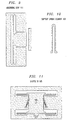
- FIG. 8 shows details of the Latch Element, Absorbing Stop, Support Spring, and Shuttle B, respectively.
- Shown in Fig. 8 is an illustrative Latch element 104 formed in the housing portion 101 of MEMS arming device 100 and includes a cantilevered beam 701, the free end of which extends into a notch 702 formed in shuttle A, 103.
- shuttle A is in the rest position.
- the free end of cantilevered beam 701 ratchets over from notch 702 to and latches in notch 703.
- Latch elements 107 of shuttle B While the construction of the other Latch elements 107 of shuttle B are somewhat smaller than Latch element 104 they operate in the same manner when shuttle B is moved in direction 152. It should be noted that the arrangement of latch springs 104 and 107 can be reversed such that, e.g., the notches 702, 703 of latch spring 104 are located on the housing 101 and the beam 701 portion located on shuttle A.
- Figure 8 illustratively shows the construction of Absorbing Stop 109.
- Figure 9 shows the construction of support springs 102, the support springs 106 being comparable in size.
- Figure 10 shows an enlargement of shuttle B, 105, illustrating the construction thereof.
Abstract


Description
- This invention relates generally to an arming device used in fusing of projected munitions and, more particularly, to a micromechanical latching switch for use in arming device.
- Artillery shells are equipped with a safety and arming device (S&A) that permits detonation of the carried explosive only after the projectile has experienced a valid progression of physical launch conditions, including the huge initial acceleration (10,000-80,000g). The arming device functions with sequential interlocks to remove a barrier in the fire train and/or to move out-of-line fire-train components into alignment. Once armed, the device can be fused with, e.g., an electrical discharge or a laser pulse. For safety, the S&A is required to be able to withstand a munitions mishandling drop from 40ft. without damage or arming.
- A typical arming device is centimeter sized and piece part assembled using screws, pins, springs, and tight-tolerance machined components. Shelf life is affected by the use of dissimilar materials and by the need for lubrication. Recent arming device modernizing efforts have been motivated by lower cost, weight, and volume. One such arrangement described by C. H. Robinson in U. S. Patent No. 6,167,809 entitled "Ultra-Miniature, Monolithic, Mechanical Safety-and-Arming Device for Projected Munitions" is directed towards a monolithic metal (nickel) device fabricated using the LIGA micro machining process.
- Notwithstanding the recent improvements made in these arming devices, there is a continuing need for further miniaturization and improved safety of arming devices.
- In accordance with the present invention, a micro-electrical-mechanical-switch (MEMS) arming device is formed from a micromachined monolithic semiconductor device having multiple-interlocks that is partially armed by the launch acceleration and fully armed by on-demand thermal activation.
- More particularly, my MEMS monolithic semiconductor device comprises
a semiconductor wafer, a first dielectric layer formed on the semiconductor wafer, and a second semiconductor layer formed on the first layer;
a first latching movable shuttle formed in the second layer and having the first layer removed under the first shuttle, the first shuttle being moved in a first direction relative to the wafer in response to a predetermined acceleration of the MEMS device in a direction opposite to the first direction, so as to change an operating condition of the MEMS device from a first switch state to an intermediate switch state;
a second latching moveable shuttle formed within the first shuttle, the second shuttle being moved in a second direction relative to the first shuttle in response to a thermally activated force so as to change the operating state of the MEMS device from the intermediate switch state to a second switch state; and
wherein in the second switch state an opening in the second shuttle aligns with an opening in the wafer to enable an optical signal to pass through the aligned openings. - In a second embodiment, my MEMS, monolithic semiconductor device comprises
a semiconductor wafer, a first electrically insulating layer formed on the semiconductor wafer, and a second semiconductor layer formed on the first layer;
a latching movable shuttle switch formed in the second layer and having the first layer removed under the shuttle switch, the shuttle switch being moved in a first direction relative to the wafer in response to a predetermined acceleration of the MEMS device in a direction opposite to the first direction, thereby changing an operating state of the shuttle switch. - According to another feature, my MEMS device includes means for preventing the movement of the second shuttle prior to the latching of the first shuttle. Another feature includes an electrical switch for providing an electrical switch connection when the MEMS device is in the intermediate switch state. Yet another feature includes an absorbing stop formed in the second layer for limiting the movement of the first shuttle in the first direction. According to another feature the MEMS device is formed by (A) first patterning and etching the first shuttle in the second layer and stopping on the first dielectric layer, (B) patterning and etching a predetermined pattern in the semiconductor wafer from the bottom surface and stopping on the first dielectric layer, (C) etching away the exposed regions of the first dielectric layer, and (D) continuing this etch to allow undercutting sufficient to free the shuttle from the substrate.
- The present invention will be more fully appreciated by consideration of the following Detailed Description, which should be read in light of the accompanying drawings in which:
- Figs. 1A - 1C illustrate a top view of a first embodiment of my MEMS device as an arming device, respectively, when in the safe position, the partially armed position and the fully armed position.
- Fig. 2 illustrates my MEMS arming device further including an electrical interlock.
- Fig. 3 is a B - B cross section view of the MEMS arming device showing the etching processes from the top and bottom sides.
- Fig. 4 is a top view of the MEMS arming device showing, in dotted-line form, the Silicon Wafer mask used to etch shuttle A from the bottom or wafer side.
- Fig. 5 more clearly illustrates the Silicon Wafer mask, shown in dotted-line form in Fig. 4, which is used to etch shuttle A from the wafer side.
- Fig. 6 is an A - A cross section view of the MEMS arming device showing that the Oxide layer is etched away below the moveable components of top Silicon layer.
- Fig. 7 shows a second embodiment of my MEMS device having only one shuttle.
- Figs. 8 - 11 show details of the Latch Element, Absorbing Stop, Support Spring, and Shuttle B, respectively.
- Fig. 12 shows an illustrative munition including my MEMS arming device.
-
- In the following description, identical element designations in different figures represent identical elements. Additionally in the element designations, the first digit refers to the figure in which that element is first located (e.g., 101 is first located in Fig. 1).
- With reference to Figs. 1A - 1C there is shown, in accordance with the present invention, an illustrative embodiment of my micro-electrical-mechanical-switch (MEMS) device (or MEMS shutter) 100 used as an arming device. It should be noted that while my MEMS device is described for use as an arming device, it more generally can be used in other applications requiring an inertial latching switch, e.g., an automotive accelerometer. The MEMS arming device 100 is implemented as part of a fusing arrangement of a munition (also referred herein as an ordnance), the fusing arrangement being used to detonate that munition once it has been fired. In Fig. 1A, the MEMS arming device 100 is shown in a rest position (first switch state) prior to the munition being fired. In Fig. 1B the MEMS arming device 100 is shown in a partially armed position (intermediate switch state) after the munition has been fired. In Fig. 1C, the MEMS arming device 100 is shown in a fully armed position (second switch state) after the munition has been fired and then thermally activated.
- Shown in Fig. 12 is an
illustrative fusing arrangement 1201 of a munition (ordnance) 1200 including alaser 1202, my MEMS arming device 1203,ignitor 1204 and explosive charge 1205. In Fig. 12A, my MEMS arming device 1203 is shown in its rest position (Fig. 1A - prior to being fired) in which thefuse windows munition 1200 is fired and the MEMS arming device 1203 is moved to its fully armed position (Fig. 1C), thefuse windows laser 1202 signal to ignite theignitor charge 1204 and detonate 1205explosive charge 1206. In one illustrative embodiment, my MEMS arming device 100 may be implemented as part of the fusing arrangement described in the concurrently filed patent application of D. Bishop et al case 56 - 3 - 2, entitled "FUSE FOR PROJECTED ORDNANCE," Serial No. 10/xxx,xxx, which is incorporated by reference herein. - The MEMS arming device 100, as shown in Figs. 1A - 1C, is formed on a SOI wafer, illustratively shown to be 4mm high and 6mm wide. The SOI wafer is shown illustratively in Fig. 3 to be implemented on a Silicon wafer (or handle) 301 that has an Oxide layer 302 (e.g., Silicon Oxide) and a
Silicon layer 303 formed thereon. While a SOI wafer is shown in Fig. 3, it should be understood that other types of semiconductors (e.g., Germanium, Gallium Arsinide) may be used. - The MEMS arming device 100 is formed by selectively etching the
Silicon wafer 301,Oxide layer 302, and aSilicon layer 303. In Figs. 1A - 1C, theSilicon layer 303 is shown in grey and the etched-out region of the Silicon layer reveals theSilicon Oxide layer 302, shown in white. With reference to Fig. 1A, the MEMS arming device 100 is shown in its rest position (first switch state), prior to the munition being fired (Fig. 10A). The Shuttle A, 103, is formed in the Silicon layer and is supportably attached tohousing 101 using four support springs, e.g., 102. Shuttle A, 103, also includes two latch springs, e.g., 104, for latching shuttle A's position once it has moved a predetermined distance indirection 150. The latch springs 104 also restrict shuttle A's movement withinhousing 101 inonly direction 150. - Shuttle B, 105, is etched within the shuttle A, 103, and is supported by Shuttle A using four support springs, e.g., 106. Shuttle B also has two latch springs, e.g., 107 for latching shuttle B's position once it has moved a predetermined distance in direction 152. Preferably, the direction 152 is perpendicular to the
direction 151. Shuttle B has avertical extension 108 that is etched in a vertical channel of shuttle A which enables shuttle B to move essentially only in the upward vertical direction 152. The shuttle B has etched therein acircular fuse window 109. TheSilicon Wafer 301 also has acircular fuse window 110 etched therein, which is offset in both thevertical direction 153 andhorizontal direction 151 relative to fusewindow 109. - A spring-suspended absorbing
stop 111 is also etched from thehousing frame 101 to limit the movement of shuttle A in thedirection 150. Athermal actuator 112 is etched fromhousing 101 and includes twohorizontal arms 113 and a vertical push-rod 114 mounted perpendicular to the midpoint of the two arms. When an electrical current is applied tothermal actuator 112 and througharms 113, the arms are heated. This causes the arms to expand and deflect in an upward direction forcing push-rod 114 in the vertical direction 152, thereby generating an upward force (thermally activated force) applied to thevertical extension 108 of shuttle B. It should be noted that the thermal activator may, more generally, include one or more arms connected to push-rod 114. - The
arms 113 are formed to have an upward bow to insure that they deflect upward in the direction 152 when heated. As shown, as a safety feature, push-rod 114 is not aligned withextension 108 when the MEMS arming device 100 is in the rest position, shown in Fig. 1A. This prevents the operation ofthermal activator 112 from moving push-rod 114 in the direction 152 when in the rest position. This feature prevents MEMS arming device 100 from entering a fully armed state prior to the munition being fired. This provides a dual-interlock safety feature, which preventsthermal actuator 112, even if accidentally activated during the rest state, from fully arming MEMS device 100 unlessshuttle A 103 has first been latched following the firing of the munition. - As shown in Fig. 1B, the MEMS arming device 100 is in the partially armed position after the munition has been fired. When the munition is fired, the inertia of shuttle A, 103, causes it to move in the
horizontal direction 150 relative to the MEMS arming device 100 movement. The MEMS arming device 100 is designed to have a high acceleration threshold which prevents the MEMS arming device 100 from being activated by dropping or other shock forces. The threshold acceleration needed to latch shuttle A is determined essentially by the dimensions of the four support springs, e.g., 102. This feature ensures that MEMS arming device 100 is only to be activated by the substantial acceleration forces of 10,000 to 80,000g generated when the munition is fired. The absorbingstop 109 is used to limit the horizontal movement of shuttle A. The result is that shuttle A is moved horizontally in direction 150 (relative to the MEMS housing 101) and latched into the firing position by the two latches 104. With shuttle A latched, thefuse window 110 in shuttle B has also been moved horizontally indirection 150 and is now positioned vertically below thefuse window 109 in theSilicon Wafer 301. In this partially armed position (intermediate switch state), thethermal actuator 112 is now aligned below and, when thermally activated, can engage thevertical extension 108 and cause shuttle B to move in the vertical direction 152 to the fully armed position. - Shown in Fig. 1C is the MEMS arming device 100 in the fully armed position (second switch state) after the munition has been fired and the on-demand
thermal actuator 112 is pulsed in response to a pulsed activation signal. After the pulse thethermal actuator 112 returns to it original position, as shown, leaving shuttle B in its latched position. Thethermal actuator 112 provides a thermal interlock safety feature, which insures that the MEMS arming device 100 does not enter the fully armed position (second switch state) without both the activation of both the acceleration interlock and thermal interlock safety features. Thethermal actuator 112 is activated by the application of an electrical signal applied across thepads 112A. When thermally activated thearms 113 are heated, they expand and deflect upward forcing push-rod 114 in the vertical direction 152 to engage thevertical extension 108 and cause shuttle B to move vertically to the fully armed position. The two latch springs 107 latch keeping shuttle B in the fully armed position. In the fully armed position thefuse window 110 in shuttle B has been moved up vertically in direction 152 so that it is now positioned directly over thefuse window 109 in theSilicon Wafer 301. - With reference to Fig. 10B, in this fully armed position a laser 1002 signal can pass through the aligned
fuse windows detonation 1005 of explosive charge 1006. - Fig. 2 illustrates my MEMS arming device 100 further including an
electrical safety interlock 200. Theelectrical safety interlock 200 includes aswitch 201 that is etched as part of shuttle A and, consequently, switch 201 is not closed until the munition is fired. After firing, a ground signal fromlead 203 is coupled throughsprings 102, shuttle A,switch 201 to contactpad 202. This ground signal could provide a control signal to enable a control circuit (not shown) to provide an electrical signal to activate thethermal activator 112. For example this control signal may be used to activate the laser (or electrical device) that will, after thethermal actuator 112 is activated, detonate the munition. - Shown in Fig. 7 is a second embodiment of my
MEMS device 700 having only oneshuttle 703. Other than including only shuttle A,MEMS device 700 may be implemented to include all of the other elements and features of the MEMS devices shown in Figs. 1 and 2. TheMEMS device 700 is shown in its rest position and thecircular window 710 ofshuttle A 701 is shown horizontally displaced from thecircular window 709, shown in dotted-line form, in the Silicon Wafer. The MEMS device is also shown to includeelectrical switch 720. WhenMEMS device 700 undergoes a predetermined acceleration indirection 751,shuttle 701 moves in thedirection 750 relative toMEMS device 700. After acceleration,shuttle 703 has moved so that thecircular window 710 aligns withcircular window 709 andelectrical switch 720 has been closed applying a control signal to pad 721. In accordance with the present invention, the design ofMEMS device 700 can be adapted for use as an automobile accelerometer to detect inertial (deceleration) forces that occur during a car collision. In such an application,MEMS device 700 detects a predefined acceleration (i.e., deceleration of the car), which causesshuttle 703 to closeelectrical switch 720 thereby generating a control signal to initiate deployment of the air-bag. - The following discussion makes joint reference to Figs. 1 and 3. As noted previously, in Figs. 1A - 1C and 2, the
Silicon layer 303 is shown in grey and the etched-out region of the Silicon layer, which reveals theSilicon Oxide layer 302, is shown in white. Since the movable elements of MEMS arming device 100 including the shuttle A, 103, shuttle B, 107, absorbingstop 109,arms 113, push-rod 114, and switch 201 (of Fig. 2) must all be free to move relative to thehousing 101 andSilicon wafer 301, theOxide layer 302 needs to be etched away under all of these movable elements. Briefly, the MEMS device 100 is formed by (A) first patterning and etching the movable elements in the Silicon layer 303 (i.e., second layer) and stopping on the Silicon Oxide layer 302 (i.e., first dielectric layer or electrically insulating layer), (B) patterning and etching a predetermined pattern in the Silicon Wafer 301 (i.e., semiconductor wafer) from the bottom surface and stopping on theSilicon Oxide layer 302, (C) etching away the exposed regions of theSilicon oxide layer 302, and (D) continuing this etch to allow undercutting sufficient to free the moveable elements from theSilicon Wafer 301. This procedure for etching the moveable elements is more fully described in the following paragraph. - With reference to Fig. 3, there is shown an illustrative B - B cross section of the shuttle A element of Fig. 2. First the Silicon layer 303 (shown in grey in Fig. 2) has been etched away using a reactive ion etch (RIE). Next the
portion 307 of theSilicon wafer 301 is etched away using a deep reactive ion etch (DRIE). Next an oxide etching solution is applied which will etchregion 308 ofOxide layer 302 not protected by the Silicon layers 303 or 301 and then etch theregions 305 ofOxide layer 302 located under the Silicon layers 303 and 301.. This is shown illustratively in Fig. 6 where theregion 601 ofOxide layer 302 below the moveable elements shuttle A, 103 (including switch 201) and absorbingstop 109 has been etched away enabling these elements to be suspended fromhousing 101 and free to move. The shuttle A, 103 is suspended fromhousing 101 by its four support springs 102 and absorbingstop 109 is also suspended fromhousing 101. - Fig. 4 is a top view of the MEMS arming device 100 showing the various areas of
Silicon wafer 301, in dotted lines, that are to be etched from the bottom orSilicon wafer 301 side. To insure that theentire Oxide layer 302 is removed below the moveable elements, theSilicon wafer 301 side is etched in the regions 401 - 404 exposing the bottom side ofOxide layer 302. As a result, the "X" shapedregion 405 and other areas as well as the perimeter portion of thehousing 101 ofSilicon wafer 301 serve as a mask to define the bottom side regions ofOxide layer 302 to be etched. Thefuse window 107 opening is also etched inSilicon Wafer 301. The resulting dotted line shaped mask of Fig. 4 is shown in Fig. 5. The bottom side ofOxide layer 302 that has been exposed by the silicon wafer mask of Fig. 5, i.e., regions 401 - 404, can then be etched away. This is shown illustratively in the cross section Fig. 6, where theOxide region 601 below the moveable elements shuttle A, 103 (including switch 201) and absorbingstop 109 has been etched away. Thus, by etching theOxide layer 302 from both the top side and the bottom side I am able to remove theentire Oxide layer 302 from beneath the moveable elements of MEMS arming device 100. - Figures 8 - 11 show details of the Latch Element, Absorbing Stop, Support Spring, and Shuttle B, respectively. Shown in Fig. 8 is an
illustrative Latch element 104 formed in thehousing portion 101 of MEMS arming device 100 and includes a cantileveredbeam 701, the free end of which extends into a notch 702 formed in shuttle A, 103. As depicted shuttle A is in the rest position. When shuttle A moves in thedirection 150 in response to the firing of the munition, the free end ofcantilevered beam 701 ratchets over from notch 702 to and latches innotch 703. While the construction of theother Latch elements 107 of shuttle B are somewhat smaller thanLatch element 104 they operate in the same manner when shuttle B is moved in direction 152. It should be noted that the arrangement of latch springs 104 and 107 can be reversed such that, e.g., thenotches 702, 703 oflatch spring 104 are located on thehousing 101 and thebeam 701 portion located on shuttle A. - Figure 8 illustratively shows the construction of Absorbing
Stop 109. Figure 9 shows the construction of support springs 102, the support springs 106 being comparable in size. Figure 10 shows an enlargement of shuttle B, 105, illustrating the construction thereof. - Various modifications of this invention will occur to those skilled in the art. Nevertheless all deviations from the specific teachings of this specification that basically rely upon the principles and their equivalents through which the art has been advanced are properly considered within the scope of the invention as described and claimed.
Claims (11)
- A micro-electrical-mechanical-switch, MEMS, monolithic semiconductor device comprising
a semiconductor wafer, a first dielectric layer formed on the semiconductor wafer, and a second semiconductor layer formed on the first layer;
a first latching movable shuttle formed in the second layer and having the first layer removed under the first shuttle, the first shuttle being moved in a first direction relative to the wafer in response to a predetermined acceleration of the MEMS device in a direction opposite to the first direction so as to change an operating condition of the MEMS device from a first switch state to an intermediate switch state;
a second latching moveable shuttle formed within the first shuttle, the second shuttle being moved in a second direction relative to the first shuttle in response to a thermally activated force so as to change the operating state of the MEMS device from the intermediate switch state to a second switch state; and
wherein in the second switch state an opening in the second shuttle aligns with an opening in the wafer to enable an optical signal to pass through the aligned openings. - The MEMS device of claim 1 further comprising
means for preventing the movement of the second shuttle prior to the movement of the first shuttle. - The MEMS device of claim 1 further comprising
an electrical switch for providing an electrical switch connection when the MEMS device is in the intermediate state. - The MEMS device of claim 1 further comprising
an absorbing stop formed in the second layer for limiting the movement of the first shuttle in the first direction. - The MEMS device of claim 1 further comprising
a thermal activator responsive to an electrical signal for generating the thermally activated force. - The MEMS device of claim 1 being formed byA. first patterning and etching the movable elements in the second layer and stopping on the first dielectric layer,B. patterning and etching a predetermined pattern in the semiconductor wafer from the bottom surface and stopping on the first dielectric layer,C. etching away the exposed regions of the first dielectric layer, andD. continuing this etch to allow undercutting sufficient to free the moveable elements from the semiconductor wafer.
- A micro-electrical-mechanical-switch, MEMS, monolithic semiconductor device comprising
a semiconductor wafer, a first electrically insulating layer formed on the semiconductor wafer, and a second semiconductor layer formed on the first layer;
a latching movable shuttle switch formed in the second layer and having the first layer removed under the shuttle switch, the shuttle switch being moved in a first direction relative to the wafer in response to a predetermined acceleration of the MEMS device in a direction opposite to the first direction, thereby changing an operating state of the shuttle switch. - The MEMS device of claim 7 wherein the shuttle switch includes
an electrical switch for providing an electrical switch connection when the MEMS device has undergone the predetermined acceleration. - The MEMS device of claim 7 wherein
the shuttle switch includes a first circular window formed therein which is vertically aligned but horizontally displaced from a second circular window formed in the wafer, and wherein in response to the MEMS device undergoing the predetermined acceleration the shuttle switch is moved so that the first circular window is horizontally moved in the first direction to be aligned over the second circular window, to thereby enable an optical signal to pass through the first and second circular windows. - The MEMS device of claim 7 further comprising
an absorbing stop formed in the second layer for limiting the movement of the shuttle switch in the first direction. - A method of operating a MEMS monolithic semiconductor device comprising a semiconductor wafer, a first dielectric layer formed on the semiconductor wafer, and a second semiconductor layer formed on the first layer, the method comprising the steps of:latching a first movable shuttle formed in the second layer and having the first layer removed under the first movable shuttle, the first movable shuttle being moved in a first direction relative to the wafer in response to a predetermined acceleration of the MEMS device in a direction opposite to the first direction; the latched first movable shuttle changing a operating state of the MEMS switch from a first state to an intermediate state andlatching a second moveable shuttle formed within the first shuttle, the second shuttle being moved in a second direction relative to the first shuttle in response to a thermally activated force so as to change the operating state of the MEMS switch device from the intermediate state to a second state.
Applications Claiming Priority (2)
| Application Number | Priority Date | Filing Date | Title |
|---|---|---|---|
| US766451 | 2004-01-27 | ||
| US10/766,451 US7142087B2 (en) | 2004-01-27 | 2004-01-27 | Micromechanical latching switch |
Publications (2)
| Publication Number | Publication Date |
|---|---|
| EP1559987A1 true EP1559987A1 (en) | 2005-08-03 |
| EP1559987B1 EP1559987B1 (en) | 2007-09-05 |
Family
ID=34654334
Family Applications (1)
| Application Number | Title | Priority Date | Filing Date |
|---|---|---|---|
| EP05250061A Expired - Fee Related EP1559987B1 (en) | 2004-01-27 | 2005-01-07 | Micromechanical latching switch |
Country Status (5)
| Country | Link |
|---|---|
| US (1) | US7142087B2 (en) |
| EP (1) | EP1559987B1 (en) |
| JP (1) | JP4718846B2 (en) |
| KR (1) | KR101128139B1 (en) |
| DE (1) | DE602005002277T2 (en) |
Cited By (6)
| Publication number | Priority date | Publication date | Assignee | Title |
|---|---|---|---|---|
| US7490553B2 (en) | 2005-10-27 | 2009-02-17 | Giat Industries | Pyrotechnic safety device of reduced dimensions |
| FR2932561A1 (en) * | 2008-06-11 | 2009-12-18 | Nexter Munitions | MICRO INITIATOR SECURE |
| EP2482028A1 (en) | 2011-01-31 | 2012-08-01 | NEXTER Munitions | Security and weaponry device with breakable bolt |
| EP2482029A1 (en) | 2011-01-31 | 2012-08-01 | NEXTER Munitions | Device for timing a movement of a micro-machined balance weight and security and weaponry device including such a timer device |
| CN110285725A (en) * | 2019-05-31 | 2019-09-27 | 北京理工大学 | A kind of Manufacturing resource security system and its implementation applied to Small cartridge |
| CN112259413A (en) * | 2020-09-18 | 2021-01-22 | 西安交通大学 | Physical latching MEMS switch based on liquid metal |
Families Citing this family (14)
| Publication number | Priority date | Publication date | Assignee | Title |
|---|---|---|---|---|
| US7371982B2 (en) * | 2005-07-29 | 2008-05-13 | Lucent Technologies Inc. | MEMS safety and arming devices having launch and rotation interlocks and method of manufacturing the same |
| US20070096860A1 (en) * | 2005-11-02 | 2007-05-03 | Innovative Micro Technology | Compact MEMS thermal device and method of manufacture |
| US8191477B1 (en) * | 2005-12-15 | 2012-06-05 | Sandia Corporation | Microelectromechanical safe arm device |
| US7398734B1 (en) * | 2006-03-09 | 2008-07-15 | The United States Of America As Represented By The Secretary Of The Navy | MEMS resettable timer |
| US7893799B1 (en) * | 2007-04-11 | 2011-02-22 | Microstar Technologies, LLC | MEMS latching high power switch |
| US7819062B2 (en) | 2007-07-17 | 2010-10-26 | Alcatel-Lucent Usa Inc. | Safety and arming device for high-G munitions |
| US7490552B1 (en) * | 2007-07-31 | 2009-02-17 | The United States Of America As Represented By The Secretary Of The Navy | MEMS microdetonator/initiator apparatus for a MEMS fuze |
| US7971532B1 (en) | 2008-12-15 | 2011-07-05 | The United States Of America As Represented By The Secretary Of The Navy | Microelectromechanical systems ignition safety device |
| EP2395533B1 (en) | 2010-06-09 | 2014-04-30 | Fraunhofer-Gesellschaft zur Förderung der angewandten Forschung e.V. | Electrostatically actuated micro-mechanical switching device |
| US8640620B1 (en) * | 2012-03-05 | 2014-02-04 | The United States Of America As Represented By The Secretary Of The Army | Non-inertial safe and arm device |
| CN109307457B (en) * | 2018-09-05 | 2021-06-11 | 南京理工大学 | Micro-electromechanical sequential logic ignition control device |
| CN110571069B (en) * | 2019-08-20 | 2021-07-02 | 南京理工大学 | Micro-mechanical collision switch control device |
| CN111272031B (en) * | 2020-03-18 | 2021-01-15 | 西安交通大学 | Bistable MEMS security device with inertia time delay function |
| CN113130259B (en) * | 2021-04-27 | 2023-01-24 | 中国工程物理研究院电子工程研究所 | Plane unit moving driven bistable MEMS switch |
Citations (7)
| Publication number | Priority date | Publication date | Assignee | Title |
|---|---|---|---|---|
| US6064013A (en) * | 1997-01-30 | 2000-05-16 | The United States Of America As Represented By The Secretary Of The Army | Miniature, planar, inertially-damped, inertially-actuated delay slider actuator |
| US6074890A (en) * | 1998-01-08 | 2000-06-13 | Rockwell Science Center, Llc | Method of fabricating suspended single crystal silicon micro electro mechanical system (MEMS) devices |
| US6130464A (en) * | 1997-09-08 | 2000-10-10 | Roxburgh Ltd. | Latching microaccelerometer |
| US6167809B1 (en) | 1998-11-05 | 2001-01-02 | The United States Of America As Represented By The Secretary Of The Army | Ultra-miniature, monolithic, mechanical safety-and-arming (S&A) device for projected munitions |
| US6314887B1 (en) * | 2000-02-22 | 2001-11-13 | The United States Of America As Represented By The Secretary Of The Army | Microelectromechanical systems (MEMS)-type high-capacity inertial-switching device |
| US6321654B1 (en) * | 2000-02-22 | 2001-11-27 | The United States Of America As Represented By The Secretary Of The Army | Microelectromechanical systems (MEMS) -type devices having latch release and output mechanisms |
| US6568329B1 (en) * | 2002-09-27 | 2003-05-27 | The United States Of America As Represented By The Secretary Of The Army | Microelectromechanical system (MEMS) safe and arm apparatus |
Family Cites Families (5)
| Publication number | Priority date | Publication date | Assignee | Title |
|---|---|---|---|---|
| FR2646901B1 (en) | 1989-05-12 | 1994-04-29 | Aerospatiale | PHOTOPYROTECHNICAL PRIMING DEVICE COMPRISING A MICROLENTIL CRIMPED BY A MEMORY MATERIAL AND PYROTECHNIC CHAIN USING THE SAME |
| US5502300A (en) * | 1993-03-31 | 1996-03-26 | Santa Barbara Research Center | Compound optically tipped detectors |
| FR2760266B1 (en) | 1997-02-28 | 1999-05-21 | Tda Armements Sas | MULTI-POINT FIRE DEVICE |
| AU2002363529A1 (en) * | 2001-11-09 | 2003-05-19 | Coventor, Incorporated | Micro-scale interconnect device with internal heat spreader and method for fabricating same |
| US6964231B1 (en) * | 2002-11-25 | 2005-11-15 | The United States Of America As Represented By The Secretary Of The Army | Miniature MEMS-based electro-mechanical safety and arming device |
-
2004
- 2004-01-27 US US10/766,451 patent/US7142087B2/en not_active Expired - Fee Related
-
2005
- 2005-01-07 EP EP05250061A patent/EP1559987B1/en not_active Expired - Fee Related
- 2005-01-07 DE DE602005002277T patent/DE602005002277T2/en active Active
- 2005-01-26 KR KR1020050006999A patent/KR101128139B1/en not_active IP Right Cessation
- 2005-01-27 JP JP2005019084A patent/JP4718846B2/en not_active Expired - Fee Related
Patent Citations (7)
| Publication number | Priority date | Publication date | Assignee | Title |
|---|---|---|---|---|
| US6064013A (en) * | 1997-01-30 | 2000-05-16 | The United States Of America As Represented By The Secretary Of The Army | Miniature, planar, inertially-damped, inertially-actuated delay slider actuator |
| US6130464A (en) * | 1997-09-08 | 2000-10-10 | Roxburgh Ltd. | Latching microaccelerometer |
| US6074890A (en) * | 1998-01-08 | 2000-06-13 | Rockwell Science Center, Llc | Method of fabricating suspended single crystal silicon micro electro mechanical system (MEMS) devices |
| US6167809B1 (en) | 1998-11-05 | 2001-01-02 | The United States Of America As Represented By The Secretary Of The Army | Ultra-miniature, monolithic, mechanical safety-and-arming (S&A) device for projected munitions |
| US6314887B1 (en) * | 2000-02-22 | 2001-11-13 | The United States Of America As Represented By The Secretary Of The Army | Microelectromechanical systems (MEMS)-type high-capacity inertial-switching device |
| US6321654B1 (en) * | 2000-02-22 | 2001-11-27 | The United States Of America As Represented By The Secretary Of The Army | Microelectromechanical systems (MEMS) -type devices having latch release and output mechanisms |
| US6568329B1 (en) * | 2002-09-27 | 2003-05-27 | The United States Of America As Represented By The Secretary Of The Army | Microelectromechanical system (MEMS) safe and arm apparatus |
Cited By (10)
| Publication number | Priority date | Publication date | Assignee | Title |
|---|---|---|---|---|
| US7490553B2 (en) | 2005-10-27 | 2009-02-17 | Giat Industries | Pyrotechnic safety device of reduced dimensions |
| FR2932561A1 (en) * | 2008-06-11 | 2009-12-18 | Nexter Munitions | MICRO INITIATOR SECURE |
| WO2010000972A1 (en) * | 2008-06-11 | 2010-01-07 | Nexter Munitions | Safe micro-initiator |
| EP2482028A1 (en) | 2011-01-31 | 2012-08-01 | NEXTER Munitions | Security and weaponry device with breakable bolt |
| EP2482029A1 (en) | 2011-01-31 | 2012-08-01 | NEXTER Munitions | Device for timing a movement of a micro-machined balance weight and security and weaponry device including such a timer device |
| FR2971048A1 (en) * | 2011-01-31 | 2012-08-03 | Nexter Munitions | SECURITY AND ARMING DEVICE WITH A CASSABLE LATCH |
| US8689690B2 (en) | 2011-01-31 | 2014-04-08 | Nexter Munitions | Safety and arming device with breakable lock |
| US8714090B2 (en) | 2011-01-31 | 2014-05-06 | Nexter Munitions | Time control device for the movement of a micro-machined and safety and arming device comprising such a time control device |
| CN110285725A (en) * | 2019-05-31 | 2019-09-27 | 北京理工大学 | A kind of Manufacturing resource security system and its implementation applied to Small cartridge |
| CN112259413A (en) * | 2020-09-18 | 2021-01-22 | 西安交通大学 | Physical latching MEMS switch based on liquid metal |
Also Published As
| Publication number | Publication date |
|---|---|
| DE602005002277T2 (en) | 2008-05-29 |
| US7142087B2 (en) | 2006-11-28 |
| DE602005002277D1 (en) | 2007-10-18 |
| JP2005214618A (en) | 2005-08-11 |
| JP4718846B2 (en) | 2011-07-06 |
| US20050183609A1 (en) | 2005-08-25 |
| KR101128139B1 (en) | 2012-03-23 |
| KR20050077276A (en) | 2005-08-01 |
| EP1559987B1 (en) | 2007-09-05 |
Similar Documents
| Publication | Publication Date | Title |
|---|---|---|
| EP1559987B1 (en) | Micromechanical latching switch | |
| US6314887B1 (en) | Microelectromechanical systems (MEMS)-type high-capacity inertial-switching device | |
| US6167809B1 (en) | Ultra-miniature, monolithic, mechanical safety-and-arming (S&A) device for projected munitions | |
| US7383774B1 (en) | Microelectromechanical safing and arming apparatus | |
| US6321654B1 (en) | Microelectromechanical systems (MEMS) -type devices having latch release and output mechanisms | |
| US6064013A (en) | Miniature, planar, inertially-damped, inertially-actuated delay slider actuator | |
| US7444937B2 (en) | Pyrotechnic safety device with micro-machined barrier | |
| US7552681B1 (en) | MEMS fuze assembly | |
| US6431071B1 (en) | Mems arm fire and safe and arm devices | |
| US6173650B1 (en) | MEMS emergetic actuator with integrated safety and arming system for a slapper/EFI detonator | |
| US6964231B1 (en) | Miniature MEMS-based electro-mechanical safety and arming device | |
| US8061271B2 (en) | Programmable inertial igniters for gun-fired munitions, thermal batteries and the like | |
| KR101700291B1 (en) | Dual safety device | |
| US4145971A (en) | Electronic time delay safety and arming mechanism | |
| Pezous et al. | Fabrication, assembly and tests of a MEMS-based safe, arm and fire device | |
| US7530312B1 (en) | Inertial sensing microelectromechanical (MEM) safe-arm device | |
| US7971532B1 (en) | Microelectromechanical systems ignition safety device | |
| EP1601926B1 (en) | Electronic safety and arming unit | |
| RU2457430C1 (en) | Detonating fuse protection and commutation device | |
| US3457382A (en) | Omnidirectional impact switch | |
| US8640620B1 (en) | Non-inertial safe and arm device | |
| US8191477B1 (en) | Microelectromechanical safe arm device | |
| US3771457A (en) | Multi-circuit safing and arming switch | |
| US7371982B2 (en) | MEMS safety and arming devices having launch and rotation interlocks and method of manufacturing the same | |
| US3955508A (en) | Acceleration integrating switch |
Legal Events
| Date | Code | Title | Description |
|---|---|---|---|
| PUAI | Public reference made under article 153(3) epc to a published international application that has entered the european phase |
Free format text: ORIGINAL CODE: 0009012 |
|
| 17P | Request for examination filed |
Effective date: 20050127 |
|
| AK | Designated contracting states |
Kind code of ref document: A1 Designated state(s): AT BE BG CH CY CZ DE DK EE ES FI FR GB GR HU IE IS IT LI LT LU MC NL PL PT RO SE SI SK TR |
|
| AX | Request for extension of the european patent |
Extension state: AL BA HR LV MK YU |
|
| AKX | Designation fees paid |
Designated state(s): DE FR GB |
|
| GRAP | Despatch of communication of intention to grant a patent |
Free format text: ORIGINAL CODE: EPIDOSNIGR1 |
|
| GRAS | Grant fee paid |
Free format text: ORIGINAL CODE: EPIDOSNIGR3 |
|
| GRAA | (expected) grant |
Free format text: ORIGINAL CODE: 0009210 |
|
| AK | Designated contracting states |
Kind code of ref document: B1 Designated state(s): DE FR GB |
|
| REG | Reference to a national code |
Ref country code: GB Ref legal event code: FG4D |
|
| REF | Corresponds to: |
Ref document number: 602005002277 Country of ref document: DE Date of ref document: 20071018 Kind code of ref document: P |
|
| ET | Fr: translation filed | ||
| PLBE | No opposition filed within time limit |
Free format text: ORIGINAL CODE: 0009261 |
|
| STAA | Information on the status of an ep patent application or granted ep patent |
Free format text: STATUS: NO OPPOSITION FILED WITHIN TIME LIMIT |
|
| 26N | No opposition filed |
Effective date: 20080606 |
|
| PGFP | Annual fee paid to national office [announced via postgrant information from national office to epo] |
Ref country code: DE Payment date: 20130122 Year of fee payment: 9 Ref country code: GB Payment date: 20130122 Year of fee payment: 9 Ref country code: FR Payment date: 20130213 Year of fee payment: 9 |
|
| REG | Reference to a national code |
Ref country code: GB Ref legal event code: 732E Free format text: REGISTERED BETWEEN 20131121 AND 20131127 |
|
| REG | Reference to a national code |
Ref country code: FR Ref legal event code: CD Owner name: ALCATEL-LUCENT USA INC. Effective date: 20131122 |
|
| REG | Reference to a national code |
Ref country code: FR Ref legal event code: GC Effective date: 20140410 |
|
| REG | Reference to a national code |
Ref country code: DE Ref legal event code: R119 Ref document number: 602005002277 Country of ref document: DE |
|
| GBPC | Gb: european patent ceased through non-payment of renewal fee |
Effective date: 20140107 |
|
| PG25 | Lapsed in a contracting state [announced via postgrant information from national office to epo] |
Ref country code: DE Free format text: LAPSE BECAUSE OF NON-PAYMENT OF DUE FEES Effective date: 20140801 |
|
| REG | Reference to a national code |
Ref country code: FR Ref legal event code: ST Effective date: 20140930 |
|
| REG | Reference to a national code |
Ref country code: DE Ref legal event code: R119 Ref document number: 602005002277 Country of ref document: DE Effective date: 20140801 |
|
| REG | Reference to a national code |
Ref country code: FR Ref legal event code: RG Effective date: 20141015 |
|
| PG25 | Lapsed in a contracting state [announced via postgrant information from national office to epo] |
Ref country code: GB Free format text: LAPSE BECAUSE OF NON-PAYMENT OF DUE FEES Effective date: 20140107 Ref country code: FR Free format text: LAPSE BECAUSE OF NON-PAYMENT OF DUE FEES Effective date: 20140131 |