EP1564802A2 - Thin film semiconductor device and method for fabricating the same - Google Patents
Thin film semiconductor device and method for fabricating the same Download PDFInfo
- Publication number
- EP1564802A2 EP1564802A2 EP05250353A EP05250353A EP1564802A2 EP 1564802 A2 EP1564802 A2 EP 1564802A2 EP 05250353 A EP05250353 A EP 05250353A EP 05250353 A EP05250353 A EP 05250353A EP 1564802 A2 EP1564802 A2 EP 1564802A2
- Authority
- EP
- European Patent Office
- Prior art keywords
- single crystal
- substrate
- layer
- insulating layer
- crystal semiconductor
- Prior art date
- Legal status (The legal status is an assumption and is not a legal conclusion. Google has not performed a legal analysis and makes no representation as to the accuracy of the status listed.)
- Withdrawn
Links
Images
Classifications
-
- H—ELECTRICITY
- H01—ELECTRIC ELEMENTS
- H01L—SEMICONDUCTOR DEVICES NOT COVERED BY CLASS H10
- H01L27/00—Devices consisting of a plurality of semiconductor or other solid-state components formed in or on a common substrate
- H01L27/02—Devices consisting of a plurality of semiconductor or other solid-state components formed in or on a common substrate including semiconductor components specially adapted for rectifying, oscillating, amplifying or switching and having at least one potential-jump barrier or surface barrier; including integrated passive circuit elements with at least one potential-jump barrier or surface barrier
- H01L27/12—Devices consisting of a plurality of semiconductor or other solid-state components formed in or on a common substrate including semiconductor components specially adapted for rectifying, oscillating, amplifying or switching and having at least one potential-jump barrier or surface barrier; including integrated passive circuit elements with at least one potential-jump barrier or surface barrier the substrate being other than a semiconductor body, e.g. an insulating body
- H01L27/1214—Devices consisting of a plurality of semiconductor or other solid-state components formed in or on a common substrate including semiconductor components specially adapted for rectifying, oscillating, amplifying or switching and having at least one potential-jump barrier or surface barrier; including integrated passive circuit elements with at least one potential-jump barrier or surface barrier the substrate being other than a semiconductor body, e.g. an insulating body comprising a plurality of TFTs formed on a non-semiconducting substrate, e.g. driving circuits for AMLCDs
- H01L27/1259—Multistep manufacturing methods
- H01L27/1262—Multistep manufacturing methods with a particular formation, treatment or coating of the substrate
- H01L27/1266—Multistep manufacturing methods with a particular formation, treatment or coating of the substrate the substrate on which the devices are formed not being the final device substrate, e.g. using a temporary substrate
-
- B—PERFORMING OPERATIONS; TRANSPORTING
- B65—CONVEYING; PACKING; STORING; HANDLING THIN OR FILAMENTARY MATERIAL
- B65B—MACHINES, APPARATUS OR DEVICES FOR, OR METHODS OF, PACKAGING ARTICLES OR MATERIALS; UNPACKING
- B65B65/00—Details peculiar to packaging machines and not otherwise provided for; Arrangements of such details
- B65B65/02—Driving gear
-
- F—MECHANICAL ENGINEERING; LIGHTING; HEATING; WEAPONS; BLASTING
- F16—ENGINEERING ELEMENTS AND UNITS; GENERAL MEASURES FOR PRODUCING AND MAINTAINING EFFECTIVE FUNCTIONING OF MACHINES OR INSTALLATIONS; THERMAL INSULATION IN GENERAL
- F16C—SHAFTS; FLEXIBLE SHAFTS; ELEMENTS OR CRANKSHAFT MECHANISMS; ROTARY BODIES OTHER THAN GEARING ELEMENTS; BEARINGS
- F16C19/00—Bearings with rolling contact, for exclusively rotary movement
- F16C19/02—Bearings with rolling contact, for exclusively rotary movement with bearing balls essentially of the same size in one or more circular rows
-
- F—MECHANICAL ENGINEERING; LIGHTING; HEATING; WEAPONS; BLASTING
- F16—ENGINEERING ELEMENTS AND UNITS; GENERAL MEASURES FOR PRODUCING AND MAINTAINING EFFECTIVE FUNCTIONING OF MACHINES OR INSTALLATIONS; THERMAL INSULATION IN GENERAL
- F16C—SHAFTS; FLEXIBLE SHAFTS; ELEMENTS OR CRANKSHAFT MECHANISMS; ROTARY BODIES OTHER THAN GEARING ELEMENTS; BEARINGS
- F16C19/00—Bearings with rolling contact, for exclusively rotary movement
- F16C19/22—Bearings with rolling contact, for exclusively rotary movement with bearing rollers essentially of the same size in one or more circular rows, e.g. needle bearings
-
- F—MECHANICAL ENGINEERING; LIGHTING; HEATING; WEAPONS; BLASTING
- F16—ENGINEERING ELEMENTS AND UNITS; GENERAL MEASURES FOR PRODUCING AND MAINTAINING EFFECTIVE FUNCTIONING OF MACHINES OR INSTALLATIONS; THERMAL INSULATION IN GENERAL
- F16H—GEARING
- F16H7/00—Gearings for conveying rotary motion by endless flexible members
- F16H7/06—Gearings for conveying rotary motion by endless flexible members with chains
-
- H—ELECTRICITY
- H01—ELECTRIC ELEMENTS
- H01L—SEMICONDUCTOR DEVICES NOT COVERED BY CLASS H10
- H01L21/00—Processes or apparatus adapted for the manufacture or treatment of semiconductor or solid state devices or of parts thereof
- H01L21/02—Manufacture or treatment of semiconductor devices or of parts thereof
- H01L21/02104—Forming layers
- H01L21/02107—Forming insulating materials on a substrate
- H01L21/02109—Forming insulating materials on a substrate characterised by the type of layer, e.g. type of material, porous/non-porous, pre-cursors, mixtures or laminates
- H01L21/02112—Forming insulating materials on a substrate characterised by the type of layer, e.g. type of material, porous/non-porous, pre-cursors, mixtures or laminates characterised by the material of the layer
- H01L21/02123—Forming insulating materials on a substrate characterised by the type of layer, e.g. type of material, porous/non-porous, pre-cursors, mixtures or laminates characterised by the material of the layer the material containing silicon
- H01L21/02164—Forming insulating materials on a substrate characterised by the type of layer, e.g. type of material, porous/non-porous, pre-cursors, mixtures or laminates characterised by the material of the layer the material containing silicon the material being a silicon oxide, e.g. SiO2
-
- H—ELECTRICITY
- H01—ELECTRIC ELEMENTS
- H01L—SEMICONDUCTOR DEVICES NOT COVERED BY CLASS H10
- H01L21/00—Processes or apparatus adapted for the manufacture or treatment of semiconductor or solid state devices or of parts thereof
- H01L21/02—Manufacture or treatment of semiconductor devices or of parts thereof
- H01L21/02104—Forming layers
- H01L21/02107—Forming insulating materials on a substrate
- H01L21/02225—Forming insulating materials on a substrate characterised by the process for the formation of the insulating layer
- H01L21/0226—Forming insulating materials on a substrate characterised by the process for the formation of the insulating layer formation by a deposition process
- H01L21/02263—Forming insulating materials on a substrate characterised by the process for the formation of the insulating layer formation by a deposition process deposition from the gas or vapour phase
- H01L21/02271—Forming insulating materials on a substrate characterised by the process for the formation of the insulating layer formation by a deposition process deposition from the gas or vapour phase deposition by decomposition or reaction of gaseous or vapour phase compounds, i.e. chemical vapour deposition
- H01L21/02274—Forming insulating materials on a substrate characterised by the process for the formation of the insulating layer formation by a deposition process deposition from the gas or vapour phase deposition by decomposition or reaction of gaseous or vapour phase compounds, i.e. chemical vapour deposition in the presence of a plasma [PECVD]
-
- H—ELECTRICITY
- H01—ELECTRIC ELEMENTS
- H01L—SEMICONDUCTOR DEVICES NOT COVERED BY CLASS H10
- H01L21/00—Processes or apparatus adapted for the manufacture or treatment of semiconductor or solid state devices or of parts thereof
- H01L21/02—Manufacture or treatment of semiconductor devices or of parts thereof
- H01L21/04—Manufacture or treatment of semiconductor devices or of parts thereof the devices having at least one potential-jump barrier or surface barrier, e.g. PN junction, depletion layer or carrier concentration layer
- H01L21/18—Manufacture or treatment of semiconductor devices or of parts thereof the devices having at least one potential-jump barrier or surface barrier, e.g. PN junction, depletion layer or carrier concentration layer the devices having semiconductor bodies comprising elements of Group IV of the Periodic System or AIIIBV compounds with or without impurities, e.g. doping materials
- H01L21/30—Treatment of semiconductor bodies using processes or apparatus not provided for in groups H01L21/20 - H01L21/26
- H01L21/31—Treatment of semiconductor bodies using processes or apparatus not provided for in groups H01L21/20 - H01L21/26 to form insulating layers thereon, e.g. for masking or by using photolithographic techniques; After treatment of these layers; Selection of materials for these layers
- H01L21/314—Inorganic layers
- H01L21/316—Inorganic layers composed of oxides or glassy oxides or oxide based glass
- H01L21/31604—Deposition from a gas or vapour
- H01L21/31608—Deposition of SiO2
-
- H—ELECTRICITY
- H01—ELECTRIC ELEMENTS
- H01L—SEMICONDUCTOR DEVICES NOT COVERED BY CLASS H10
- H01L21/00—Processes or apparatus adapted for the manufacture or treatment of semiconductor or solid state devices or of parts thereof
- H01L21/70—Manufacture or treatment of devices consisting of a plurality of solid state components formed in or on a common substrate or of parts thereof; Manufacture of integrated circuit devices or of parts thereof
- H01L21/71—Manufacture of specific parts of devices defined in group H01L21/70
- H01L21/76—Making of isolation regions between components
- H01L21/762—Dielectric regions, e.g. EPIC dielectric isolation, LOCOS; Trench refilling techniques, SOI technology, use of channel stoppers
- H01L21/7624—Dielectric regions, e.g. EPIC dielectric isolation, LOCOS; Trench refilling techniques, SOI technology, use of channel stoppers using semiconductor on insulator [SOI] technology
- H01L21/76251—Dielectric regions, e.g. EPIC dielectric isolation, LOCOS; Trench refilling techniques, SOI technology, use of channel stoppers using semiconductor on insulator [SOI] technology using bonding techniques
- H01L21/76254—Dielectric regions, e.g. EPIC dielectric isolation, LOCOS; Trench refilling techniques, SOI technology, use of channel stoppers using semiconductor on insulator [SOI] technology using bonding techniques with separation/delamination along an ion implanted layer, e.g. Smart-cut, Unibond
-
- H—ELECTRICITY
- H01—ELECTRIC ELEMENTS
- H01L—SEMICONDUCTOR DEVICES NOT COVERED BY CLASS H10
- H01L27/00—Devices consisting of a plurality of semiconductor or other solid-state components formed in or on a common substrate
- H01L27/02—Devices consisting of a plurality of semiconductor or other solid-state components formed in or on a common substrate including semiconductor components specially adapted for rectifying, oscillating, amplifying or switching and having at least one potential-jump barrier or surface barrier; including integrated passive circuit elements with at least one potential-jump barrier or surface barrier
- H01L27/12—Devices consisting of a plurality of semiconductor or other solid-state components formed in or on a common substrate including semiconductor components specially adapted for rectifying, oscillating, amplifying or switching and having at least one potential-jump barrier or surface barrier; including integrated passive circuit elements with at least one potential-jump barrier or surface barrier the substrate being other than a semiconductor body, e.g. an insulating body
- H01L27/1214—Devices consisting of a plurality of semiconductor or other solid-state components formed in or on a common substrate including semiconductor components specially adapted for rectifying, oscillating, amplifying or switching and having at least one potential-jump barrier or surface barrier; including integrated passive circuit elements with at least one potential-jump barrier or surface barrier the substrate being other than a semiconductor body, e.g. an insulating body comprising a plurality of TFTs formed on a non-semiconducting substrate, e.g. driving circuits for AMLCDs
-
- B—PERFORMING OPERATIONS; TRANSPORTING
- B65—CONVEYING; PACKING; STORING; HANDLING THIN OR FILAMENTARY MATERIAL
- B65B—MACHINES, APPARATUS OR DEVICES FOR, OR METHODS OF, PACKAGING ARTICLES OR MATERIALS; UNPACKING
- B65B11/00—Wrapping, e.g. partially or wholly enclosing, articles or quantities of material, in strips, sheets or blanks, of flexible material
- B65B11/04—Wrapping, e.g. partially or wholly enclosing, articles or quantities of material, in strips, sheets or blanks, of flexible material the articles being rotated
- B65B11/045—Wrapping, e.g. partially or wholly enclosing, articles or quantities of material, in strips, sheets or blanks, of flexible material the articles being rotated by rotating platforms supporting the articles
-
- F—MECHANICAL ENGINEERING; LIGHTING; HEATING; WEAPONS; BLASTING
- F16—ENGINEERING ELEMENTS AND UNITS; GENERAL MEASURES FOR PRODUCING AND MAINTAINING EFFECTIVE FUNCTIONING OF MACHINES OR INSTALLATIONS; THERMAL INSULATION IN GENERAL
- F16C—SHAFTS; FLEXIBLE SHAFTS; ELEMENTS OR CRANKSHAFT MECHANISMS; ROTARY BODIES OTHER THAN GEARING ELEMENTS; BEARINGS
- F16C2361/00—Apparatus or articles in engineering in general
- F16C2361/71—Chains
Definitions
- the present invention relates to a semiconductor device and a method for fabricating the device.
- An active-matrix-addressed display uses an active-matrix substrate on which a huge number of thin-film transistors (TFTs) are arranged in matrix.
- TFTs thin-film transistors
- Those TFTs are integrated together on a substrate of an insulating material such as glass by thin film deposition, photolithography, and other manufacturing technologies similar to normal LSI manufacturing technologies. More particularly, a silicon thin film is deposited on a substrate by a CVD process, for example, and then patterned into a plurality of islands, which will be eventually used as active areas for respective TFTs.
- the TFTs fabricated in this manner are roughly classifiable into amorphous silicon TFTs and polysilicon TFTs according to the crystallinity of the silicon thin film to be used.
- the field effect mobility of a polysilicon film is usually higher than that of an amorphous silicon film.
- a polysilicon TFT can operate faster than an amorphous silicon TFT.
- driver circuitry around the display area may consist of TFTs.
- a source driver (data driver) and other peripheral driver circuits are made up of polysilicon TFTs, then variations will arise in the threshold voltage of the transistors and other TFT characteristics, thus posing a difficult problem in practice.
- a single crystal silicon (single crystal silicon) film be used as an active layer (as a channel region) for the TFTs.
- a TFT of that type is called a "single crystal silicon TFT”.
- single crystal silicon TFTs which are high-performance devices, are bonded onto a glass substrate with an adhesive, thus resulting in low yield and poor productivity. Also, after the single crystal silicon TFTs have been bonded onto the substrate, the substrate has bonding portions of the adhesive, and therefore, has low thermal resistance and easily emits gases. Thus, it is virtually impossible to further deposit a high-quality inorganic insulating film or a different group of TFTs on the substrate on which the single crystal silicon TFTs have been bonded.
- Japanese National Stage Publication No. 7-503557 just discloses the technique of transferring prepared single crystal silicon TFTs onto a glass substrate. However, just by using those simply transferred single crystal silicon TFTs, it is impossible to obtain high-performance, high-function semiconductor devices that are in increasingly high demand these days.
- an active-matrix substrate for use in an LCD, for example, not just single crystal silicon TFTs but also polysilicon TFTs are preferably integrated on the same substrate together.
- the applicant of the present application proposed in Japanese Patent Application No. 2003-67109 a method of making an active-matrix substrate in which single crystal silicon TFTs are fabricated on a substrate by utilizing the bonding method described above and then non-single crystal silicon TFTs (e.g., polysilicon TFTs) are fabricated on the same substrate.
- a substrate 30 with an insulating surface 31 is prepared. Meanwhile, hydrogen ions are implanted at a particular dose level into a single crystal silicon substrate 50 with a silicon dioxide layer 51 on the surface, thereby forming a hydrogen ion implanted layer 55 at a predetermined depth in the single crystal silicon substrate 50 .
- a single crystal silicon layer is produced between the hydrogen ion implanted layer 55 and the silicon dioxide layer 51 and will be referred to herein as an "upper single crystal silicon layer".
- the upper single crystal silicon layer may be subjected to either a doping process to define a gate electrode or source/drain regions or a doping process to define a base, a collector and an emitter, thereby forming a thin-film transistor, the surface of which may subsequently be planarized and made hydrophilic.
- the single crystal silicon substrate 50 in which the hydrogen ion implanted layer 55 has been produced, and the substrate 30 are bonded together such that the silicon dioxide layer 51 of the single crystal silicon substrate 50 is in contact with the insulating surface 31 of the substrate 30 .
- these substrates 30 and 50 are heated to a temperature at which hydrogen ions dissociate themselves from silicon in the hydrogen ion implanted layer 55 .
- the surface of the single crystal silicon substrate 50 i.e., the silicon dioxide layer 51
- the insulating surface 31 can be bonded together even more strongly.
- micro bubbles are produced in the hydrogen ion implanted layer 55 , thereby making the silicon dioxide layer 51 and upper single crystal silicon layer cleavable and removable at the hydrogen ion implanted layer 55 from the single crystal silicon substrate 50.
- a bonded substrate 60 including the single crystal silicon layer 52 and MOS single crystal silicon TFTs, can be obtained without using adhesive as shown in FIG. 6C.
- the bonded substrate 60 has a structure in which the surface portion of the single crystal silicon substrate 50 above the hydrogen ion implanted layer 55 (i.e., the upper single crystal silicon layer and the silicon dioxide layer 51) is bonded to the substrate 30.
- a big level difference is created between a portion of the bonded substrate 60, to which that surface portion has been bonded (i.e., bonding portion), and the other portions thereof.
- This level difference is greater than the thickness of the silicon dioxide layer 51 (which is normally in the range of about 100 nm to about 500 nm).
- an insulating film 56 of SiO 2 for example, and an amorphous silicon film 57 are deposited in this order over the entire surface of the substrate 60 .
- the amorphous silicon film 57 is crystallized into a polysilicon film 57p .
- the polysilicon film 57p is patterned into a patterned polysilicon layer 57', which is then covered with a gate insulating film 58 of SiO 2 .
- a conductor film (not shown) is deposited on the gate insulating film 58 and then etched into the pattern of gate electrodes 59.
- the surface of the substrate 60 is further covered with a passivation film and an interlayer dielectric film 62.
- metal interconnects 61 are defined on the interlayer dielectric film 62 so as to be electrically connected to the polysilicon layer 57' and single crystal silicon layer 52 through contact holes that have been provided through the interlayer dielectric film 62 and so on. In this manner, single crystal silicon TFTs and polysilicon TFTs can be fabricated on the same substrate.
- the gate electrodes 59 are usually defined by patterning the conductor film (not shown), which has been deposited on the gate insulating film 58, by a dry etching process (see FIG. 6F). In this process step, there are some deep stepped portions 70 on the surface of the substrate 60. Accordingly, some residues of the conductor film may remain on the side surface of those stepped portions 70. Also, if interconnects are defined so as to cross the stepped portions 70, then the interconnects are more likely to disconnect.
- fine-line interconnects may disconnect or some conductor may be left on the stepped surface portions of the substrate even after the dry etching process, thus possibly affecting the reliability and the yield of the resultant device.
- an object of the present invention is to reduce the level difference to be created on the surface of a substrate when a single crystal semiconductor layer is bonded onto the substrate.
- a semiconductor device preferably includes a substrate with an insulating surface and a single crystal semiconductor layer, which is bonded to the insulating surface of the substrate.
- the device preferably further includes a first insulating layer, which is provided between the insulating surface of the substrate and the single crystal semiconductor layer, and a second insulating layer, which has been deposited on the entire insulating surface of the substrate except an area in which the first insulating layer is present.
- every edge of the second insulating layer is preferably aligned with its associated edge of the first insulating layer.
- the thickness of the first insulating layer is preferably substantially equal to that of the second insulating layer.
- the semiconductor device preferably further includes a non-single crystal semiconductor layer on the second insulating layer.
- An electronic device including semiconductor devices preferably includes: a substrate with an insulating surface; a single crystal semiconductor layer, which is bonded onto a selected area of the insulating surface of the substrate; a first insulating layer, which is provided between the insulating surface of the substrate and the single crystal semiconductor layer; a second insulating layer, which has been deposited on the entire insulating surface except the selected area where the first insulating layer is present; a single crystal semiconductor device, which has been fabricated over the first insulating layer so as to include at least a portion of the single crystal semiconductor layer; and a non-single crystal semiconductor device, which has been fabricated on the second insulating layer.
- every edge of the second insulating layer is preferably aligned with its associated edge of the first insulating layer.
- the thickness of the first insulating layer is preferably substantially equal to that of the second insulating layer.
- the non-single crystal semiconductor device includes at least a portion of a non-single crystal semiconductor layer provided on the second insulating layer.
- the single crystal semiconductor device is preferably a thin-film transistor, which includes at least the portion of the single crystal semiconductor layer as a channel region
- the non-single crystal semiconductor device is preferably a thin-film transistor, which includes at least the portion of the non-single crystal semiconductor layer as a channel region.
- the electronic device preferably further includes a third insulating layer, which is located between the second insulating layer and the non-single crystal semiconductor layer and between the single crystal semiconductor layer and the non-single crystal semiconductor layer.
- the single crystal semiconductor device preferably further includes a gate electrode on the third insulating layer.
- the non-single crystal semiconductor device preferably further includes a gate insulating film, which covers the non-single crystal semiconductor layer, and a gate electrode on the gate insulating film.
- the third insulating layer is preferably thinner than the gate insulating film of the non-single crystal semiconductor device.
- the gate electrode of the single crystal semiconductor device and a channel region of the non-single crystal semiconductor device may be made of the same polycrystalline semiconductor film.
- a method for fabricating a semiconductor device preferably includes the steps of (a) preparing a single crystal semiconductor substrate that includes: a first insulating layer, which covers the surface of the substrate; an ion implanted layer, which is located at a predetermined depth as measured from the surface and which includes hydrogen ions and/or ions of a rare gas; and a single crystal semiconductor layer, which is located between the first insulating layer and the ion implanted layer, (b) preparing a supporting substrate with an insulating surface, (c) bonding the single crystal semiconductor substrate onto a selected area of the insulating surface of the supporting substrate such that the first insulating layer contacts with the insulating surface of the supporting substrate, (d) depositing a second insulating layer over the supporting substrate such that the single crystal semiconductor substrate is covered with the second insulating layer, and (e) removing a portion of the second insulating layer, which covers the single crystal semiconductor substrate, and a portion of the single crystal semiconductor substrate itself from the
- the step (d) preferably includes depositing the second insulating layer such that the thickness of the second insulating layer becomes substantially equal to, or greater than, that of the first insulating layer.
- the step (d) includes depositing the second insulating layer at a temperature of 350 °C or less.
- the step (e) preferably includes heating the single crystal semiconductor substrate to a temperature of 400 °C to 650 °C , thereby separating the single crystal semiconductor layer from the single crystal semiconductor substrate.
- the method may further include, after the step (e), the step of (f) selectively etching, and reducing the thicknesses of, the second insulating layer and the single crystal semiconductor layer, thereby substantially equalizing the thickness of the second insulating layer with that of the first insulating layer.
- the method may further include the step of (d2) depositing an amorphous semiconductor film on the second insulating layer after the step (d) and before the step (e).
- the step (e) preferably includes removing hydrogen atoms from the amorphous semiconductor film while separating the single crystal semiconductor layer from the single crystal semiconductor substrate.
- a method for fabricating an electronic device including semiconductor devices preferably includes the steps of (a) preparing a single crystal semiconductor substrate that includes: a first insulating layer, which covers the surface of the substrate; an ion implanted layer, which is located at a predetermined depth as measured from the surface and which includes hydrogen ions and/or ions of a rare gas; and a single crystal semiconductor layer, which is located between the first insulating layer and the ion implanted layer, (b) preparing a supporting substrate with an insulating surface, (c) bonding the single crystal semiconductor substrate onto a selected area of the insulating surface of the supporting substrate such that the first insulating layer contacts with the insulating surface of the supporting substrate, (d) depositing a second insulating layer over the supporting substrate such that the single crystal semiconductor substrate is covered with the second insulating layer, (e) removing a portion of the second insulating layer, which covers the single crystal semiconductor substrate, and a portion of the single crystal semiconductor substrate itself from
- the method preferably further includes the step of (d2) depositing an amorphous semiconductor film on the second insulating layer after the step (d) and before the step (e).
- the method preferably further includes, between the steps (e) and (f), the steps of (g) forming a third insulating layer on the single crystal semiconductor layer and on the second insulating layer, and (h) depositing an amorphous semiconductor film on the third insulating layer.
- the step (f) may include the steps of (f2) crystallizing and turning the amorphous semiconductor film into a polycrystalline semiconductor film and (f3) patterning the polycrystalline semiconductor film.
- the step (f) may include making thin-film transistors as the single crystal semiconductor device and the non-single crystal semiconductor device.
- the step (a) may include preparing a single crystal semiconductor substrate in which multiple transistor structures, which use at least a portion of the single crystal semiconductor layer between the ion implanted layer and the first insulating layer as a channel region, have been defined at least partially.
- the step (f) may include the steps of (f2) crystallizing and turning the amorphous semiconductor film into a polycrystalline semiconductor film, and (f3) patterning the polycrystalline semiconductor film.
- the non-single crystal semiconductor device may be a thin-film transistor, which uses at least a portion of the polycrystalline semiconductor film as a channel region
- the single crystal semiconductor device may be a thin-film transistor, which uses at least another portion of the polycrystalline semiconductor film as a gate electrode.
- the step (f) may include making thin-film transistors as the single crystal semiconductor device and as the non-single crystal semiconductor device.
- the step (f) may include the steps of (f2') providing a gate electrode for the single crystal semiconductor device on the third insulating layer, (f2) crystallizing and turning the amorphous semiconductor film into a polycrystalline semiconductor film, (f3) patterning the polycrystalline semiconductor film, (f4) forming a gate insulating film that covers the patterned polycrystalline semiconductor film, and (f5) providing a gate electrode for the non-single crystal semiconductor device on the gate insulating film.
- the step (g) may include forming the third insulating layer that is thinner than the gate insulating film formed by the step (f4).
- a semiconductor device preferably includes a substrate having an SiO 2 film on the surface; and a single crystal silicon layer, which is bonded to a surface of the SiO 2 film.
- the device preferable further includes a first SiO 2 layer, which is provided between the surface of the SiO 2 film and the single crystal silicon layer, and a second SiO 2 layer, which has been deposited on the entire surface of the SiO 2 film except an area in which the first SiO 2 layer is present.
- the level difference to be created on the surface of a substrate by bonding a single crystal semiconductor layer thereto can be reduced significantly as compared with a conventional one.
- a high-reliability electronic device including a single crystal semiconductor device and a non-single crystal semiconductor device on the same substrate, can be provided. By integrating the single crystal and non-single crystal semiconductor devices together on the same substrate, a system with even higher performance is realized.
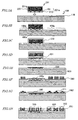
- FIGS. 1A through 1F are schematic cross-sectional views showing how to make a semiconductor device according to a principle of the present invention.
- FIGS. 2A through 2H are cross-sectional views illustrating respective process steps for fabricating a semiconductor device according to a first preferred embodiment of the present invention.
- FIGS. 3A through 3I are cross-sectional views illustrating respective process steps for fabricating a semiconductor device according to a second preferred embodiment of the present invention.
- FIGS. 4A through 4H are cross-sectional views illustrating respective process steps for fabricating a semiconductor device according to a third preferred embodiment of the present invention.
- FIGS. 5A through 5H are cross-sectional views illustrating respective process steps for fabricating a semiconductor device according to a fourth preferred embodiment of the present invention.
- FIGS. 6A through 6H are cross-sectional views illustrating a conventional method for fabricating a semiconductor device.
- a single crystal semiconductor substrate has been bonded onto a supporting substrate with an insulating surface (e.g., a glass substrate) and before a bulk portion of that single crystal semiconductor substrate is removed from the supporting substrate, an insulating film is deposited over the supporting substrate. And when the bulk portion of the single crystal semiconductor substrate is removed from the supporting substrate, excessive portions of that insulating film are also removed by a lift-off technique. By adopting this lift-off technique, no matter what shape the single crystal semiconductor substrate has, the excessive portions of the insulating film to be removed have the same shape as the single crystal semiconductor substrate. As a result, the insulating film remaining on the supporting substrate is self-aligned with the single crystal semiconductor layer that has been bonded onto the supporting substrate.
- an insulating surface e.g., a glass substrate
- FIGS. 1A through 1F a preferred embodiment of the present invention will be described in further detail with reference to FIGS. 1A through 1F.
- a single crystal semiconductor substrate including an ion implanted layer 6, is prepared.
- the ion implanted layer 6 has been produced in advance by implanting hydrogen ions and/or ions of a rare gas to a predetermined depth as measured from the surface.
- a first insulating layer 2 has also been defined on the surface of this single crystal semiconductor substrate.
- the portion located between the first insulating layer 2 and the ion implanted layer 6 is a single crystal semiconductor layer 4, while the other portion located between the ion implanted layer 6 and the lower surface of the single crystal semiconductor substrate is a bulk portion 10 .
- a supporting substrate 1 with an insulating surface 12 is prepared.
- the single crystal semiconductor substrate is bonded onto the supporting substrate 1 such that the first insulating layer 2 of the single crystal semiconductor substrate contacts with a selected area on the insulating surface 12.
- a second insulating layer 3 is deposited all over the exposed surface of the substrate 1 to which the single crystal semiconductor substrate has been bonded.
- the deposition temperature of the second insulating layer 3 is preferably lower than the temperature at which hydrogen ions dissociate themselves from the ion implanted layer 6 of the single crystal semiconductor substrate.
- the substrate 1 is annealed at a predetermined temperature, thereby splitting the single crystal semiconductor substrate into two along the ion implanted layer 6 as shown in FIG. 1E.
- the annealing temperature is typically at least 400 °C and is preferably 500 °C or more. Also, considering the thermal resistance of the substrate 1, the annealing temperature is preferably at most 650 °C and more preferably 600 °C or less. As a result of this process step, not only the bulk portion 10 of the single crystal semiconductor substrate is separated from the supporting substrate 1 but also excessive portions of the second insulating layer 3, which have covered the upper and side surfaces of the bulk portion 10, are lifted off.
- the second insulating layer 3 covers only surface areas of the substrate 1 where the first insulating layer 2 is not present. Thereafter, if necessary, surface portions of the second insulating layer 3 may be etched away from around the edges of the single crystal semiconductor layer 4, thereby planarizing the surface of the second insulating layer 3 as shown in FIG. 1F.
- a bonded substrate 20 in which the single crystal semiconductor layer 4 has been bonded onto the supporting substrate 1 can be obtained.
- the second insulating layer 3 is provided on the surface of the substrate 1 so as to be self-aligned with the first insulating layer 2 (i.e., so as not to overlap with the first insulating layer 2 ). That is, the edge of the second insulating layer 3 makes contact with its associated edge of the first insulating layer 2. Thus, a smaller level difference is created by bonding the single crystal semiconductor layer 4.
- a structure including just a substrate with an insulating surface and a single crystal semiconductor layer that has been formed on that surface is sometimes referred to as a "semiconductor device".
- the bonded substrate 20 including the single crystal semiconductor layer 4 as shown in FIG. 1F may also be referred to herein as a "semiconductor device”.
- the "substrate with an insulating surface" in a semiconductor device is typically an insulating substrate of glass but does not always have to have a plate shape.
- the thickness of the first insulating layer 2 is preferably approximately equal to that of the second insulating layer 3.
- the level difference can still be reduced sufficiently effectively.
- the final thickness of the second insulating layer 3 can also be adjusted by etching the portions of the second insulating layer 3 remaining on the supporting substrate 1.
- the final thickness of the second insulating layer 3 is preferably defined such that the absolute value of the difference in thickness (i.e., the level difference) between the first and second insulating layers 2 and 3 is at most about 100 nm, more preferably about 50 nm or less.
- single crystal semiconductor TFTs can be fabricated by using the single crystal semiconductor layer 4 that has been bonded onto the supporting substrate 1. Also, if a non-single crystal semiconductor layer is deposited on the second insulating layer 3, then single crystal semiconductor TFTs and non-single crystal semiconductor TFTs can be integrated together on the same substrate 1. Even if a circuit is made of the single crystal and non-single crystal layers on the same substrate in this manner, the level difference on the substrate surface can be reduced significantly at least, and may even be eliminated in some cases, according to the present invention. Thus, a highly reliable semiconductor device can be provided with the disconnection or short-circuit of the interconnects minimized.
- the bonded substrate 20 is applicable for use in various electronic devices with semiconductor devices.
- the "electronic device including semiconductor devices” broadly refers to any electronic device including at least two semiconductor devices, e.g., an active-matrix substrate, an LCD, an organic EL display, an LSI, and so forth.
- such an electronic device including semiconductor devices may be an active-matrix substrate that includes a single crystal silicon TFT on the first insulating layer 2 and a polysilicon TFT on the second insulating layer 3.
- the single crystal silicon TFT may use at least a portion of the single crystal semiconductor layer (single crystal silicon layer) 4 as its channel region.
- the polysilicon TFT may use a polysilicon layer on the second insulating layer 3 as its channel region. Furthermore, the gate electrode of the single crystal silicon TFT and the channel region of the non-single crystal silicon TFT may be made of the same polycrystalline semiconductor film.
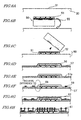
- FIGS. 2A through 2H a first specific preferred embodiment of the present invention will be described with reference to FIGS. 2A through 2H .
- a supporting substrate 100 and a single crystal silicon substrate 200 are prepared. Although only one single crystal silicon substrate 200 is illustrated in FIG. 2A , the number of single crystal silicon substrates 200 to be bonded onto the single supporting substrate 100 does not have to be one but may be two or more.
- the supporting substrate 100 is a glass substrate Code 1737 (produced by Corning Inc.) on which an SiO 2 film 110 has been deposited to a thickness of about 100 nm.
- This SiO 2 film 110 may be deposited by a plasma CVD process using tetraethylorthosilicate (TEOS) and oxygen gases.
- TEOS tetraethylorthosilicate
- the SiO 2 film 110 may be omitted depending on the material of the substrate.
- the glass substrate Code 1737 it is not always necessary to deposit an insulating film on its surface.
- the supporting substrate 100 has only to have an insulating surface and not the overall supporting substrate 100 has to be made of an electrically insulating material.
- a first SiO 2 film 210 is deposited to a thickness of 50 nm to 100 nm, for example, on the surface of a single crystal silicon wafer.
- the first SiO 2 film 210 has a thickness of about 100 nm.
- the supporting substrate 100 has no insulating film 110, then the first SiO 2 film 210 of the single crystal silicon substrate 200 is preferably relatively thick (e.g., in the range of 200 nm to 300 nm) to stabilize the characteristics.
- a hydrogen ion implanted layer 220 is formed at a predetermined depth in the single crystal silicon wafer.
- the thickness of the single crystal silicon layer to be bonded onto the supporting substrate can be defined by the depth of the hydrogen ion implanted layer 220 produced.
- the hydrogen ion implanted layer 220 may be located at a depth of about 500 nm, for example.
- the hydrogen ion implanted layer 220 may be formed by implanting hydrogen ions at a predetermined dose (e.g., 5 ⁇ 10 16 /cm 2 ).
- a predetermined dose e.g., 5 ⁇ 10 16 /cm 2
- not only the hydrogen ions but also ions of a rare gas may be implanted as well.
- the hydrogen ions need to be implanted in a reduced dose to cleave and separate the bulk of the single crystal silicon substrate 200. And when the implant dose of hydrogen ions decreases, complex defects to be generated through hydrogen-acceptor bonding can be minimized and the deterioration in device performance due to the hydrogen implantation can be avoided. Since the rare gas ions have a greater mass than the hydrogen ions, the implantation of the rare gas ions causes a greater damage on the silicon wafer than the implantation of the hydrogen ions. Thus, the implant doses need to be appropriately determined according to the device performance required. In this preferred embodiment, hydrogen ions and He ions are implanted into the silicon wafer at an implant dose of 1 ⁇ 10 16 /cm 2 and at an implant dose of 3 ⁇ 10 16 /cm 2 , respectively.
- the silicon wafer prepared in this manner is cut into at least one single crystal silicon substrate 200 with a predetermined size and shape.
- the size and shape of the single crystal silicon substrate 200 are determined according to the size and shape of the single crystal semiconductor layer to be bonded onto the supporting substrate 100. If the single crystal silicon substrate 200 has a relatively small size, then the single silicon wafer may be diced into a plurality of single crystal silicon substrates 200. Also, if a lot of single crystal silicon substrates 200 are bonded onto the same supporting substrate 100, those single crystal silicon substrates 200 may have been cut out of respectively different silicon wafers.
- the portion between the hydrogen ion implanted layer 220 and the first SiO 2 film 210 will be referred to herein as a single crystal silicon layer 190, while the other portion deeper than the hydrogen ion implanted layer 220 will be referred to herein as a bulk portion 200b.
- the single crystal silicon layer 190 and the first SiO 2 film 210 will be collectively referred to herein as a "surface region 200a".
- the surfaces of the supporting substrate 100 and single crystal silicon substrate 200 are ultrasonic cleaned (may even be megasonic cleaned) in an SC-1 solution (i.e., a mixture of ammonia, hydrogen peroxide and deionized water) and then rinsed with ultrapure water, thereby removing foreign particles from the surfaces and activating the surfaces of these substrates.
- SC-1 solution i.e., a mixture of ammonia, hydrogen peroxide and deionized water
- the single crystal silicon substrate 200 and the supporting substrate 100 are bonded together in a predetermined area 100s at room temperature, thereby obtaining a bonded substrate.
- these substrates 200 and 100 are bonded together such that the insulating film 110 of the supporting substrate 100 contacts with the first SiO 2 film 210 of the single crystal silicon substrate 200.
- the area 100s to which the single crystal silicon substrate 200 has been bonded will be referred to herein as a "single crystal semiconductor device area 100s", while the other area will be referred to herein as a “non-single crystal semiconductor device area 100p”.
- a second SiO 2 film 230 and an a-Si film 240 are deposited in this order to thicknesses of about 100 nm and about 50 nm, respectively, by a plasma CVD process, for example, so as to cover the entire exposed surface of the bonded substrate.
- the temperature of the bonded substrate is preferably maintained at least equal to 250 °C but at most equal to the hydrogen dissociation temperature (e.g., equal to or lower than 350 °C).
- the thickness of the second SiO 2 film 230 is preferably approximately equal to that of the first SiO 2 film 210.
- the bonded substrate is preferably annealed at a temperature of at least about 400 °C, more preferably at a temperature of 500 °C to 600 °C.
- hydrogen atoms dissociate themselves from the a-Si film 240 and the single crystal silicon substrate 200 splits along the hydrogen ion implanted layer 220. That is to say, the bulk portion 200b of the single crystal silicon substrate 200 comes off the bonded substrate.
- portions of the second SiO 2 film 230 and a-Si film 240, which have covered the exposed lower and side surfaces of the single crystal silicon substrate 200 are also lifted off. Consequently, as shown in FIG.
- the surface region 200a of the single crystal silicon substrate 200 i.e., the first SiO 2 film 210 and the single crystal silicon layer 190
- the second SiO 2 film 230 with a thickness of 100 nm, for example
- the a-Si (or already polycrystalline) film 240 with a thickness of 50 nm, for example
- the bonded substrate 600 shown in FIG. 2E is obtained.
- the thickness of the second SiO 2 film 230 is approximately equal to that of the first SiO 2 film 210.
- these insulating films 230 and 210 together make up a single insulating layer that has a substantially flat surface over the bonded substrate 600.
- the thickness of the second SiO 2 film 230 may be different from that of the first SiO 2 film 210.
- the absolute value of that difference is preferably at most equal to 100 nm, more preferably 50 nm or less. Then, the level difference between the areas 100s and 100p on the surface of the substrate can be reduced to 100 nm or less, preferably 50 nm or less.
- the second SiO 2 film 230 can be defined in the area 100p, other than the area 100s where the single crystal silicon layer 190 has been bonded, so as to be self-aligned with the single crystal silicon layer 190.
- the level difference between the surface areas 100s and 100p on the substrate can be reduced without complicating the manufacturing process.
- high-reliability single crystal Si devices and non-single crystal Si devices can be integrated together on the same substrate 600.
- a non-single crystal silicon device can be fabricated easily on the second SiO 2 film 230 by using the a-Si film 240.
- a single crystal silicon device e.g., a single crystal silicon TFT
- a non-single crystal silicon device e.g., a non-single crystal silicon TFT
- the level difference between the single crystal silicon layer 190 and the a-Si film 240 will be small enough to further simplify the manufacturing process and increase the yield then.
- an active-matrix substrate can be made.
- the a-Si film 240 is crystallized (with a laser beam, for example) and turned into a p-Si film 240p.
- the hydrogen atoms that were contained in the a-Si film 240 have already been removed by the annealing process (FIG. 2D). For that reason, in this crystallizing process step, it is possible to prevent the p-Si film 240p from being ruptured due to rapid expansion or dissociation of those hydrogen atoms.
- This crystallizing process step may be carried out by exposing the overall substrate 600 to an excimer laser beam (such as an XeCl laser beam with a wavelength of 308 nm) at an energy density of 300 to 400 mJ/cm 2 , for example.
- an excimer laser beam such as an XeCl laser beam with a wavelength of 308 nm
- the a-Si film 240 may also be crystallized by annealing the substrate 600 in a furnace.
- the single crystal silicon layer 190 is preferably sufficiently thick. This is because in such a rather thick single crystal silicon layer 190, its surface melts but the inside portion thereof does not. More particularly, the single crystal silicon layer 190 preferably has a thickness of at least 300 nm, more preferably 500 nm or more (e.g., about 500 nm). In addition, by performing any of these crystallizing process steps, crystal defects and other defects, which were created in the single crystal silicon layer 190 due to the implantation of hydrogen ions, can be repaired sufficiently.
- portions of the second SiO 2 film 230 which are exposed around the single crystal silicon layer 190, are selectively etched away by a reactive ion etching (RIE) process, which is a kind of anisotropic etching process.
- RIE reactive ion etching
- those exposed portions of the second SiO 2 film 230 are selectively removed to a depth corresponding with the thickness of the p-Si film 240p (e.g., about 50 nm) by an RIE process using a mixture of CHF 3 , CF 4 and Ar gases.
- the single crystal silicon layer 190 is etched so as to have a predetermined thickness.
- This etching process may be carried out as an RIE process using a mixture of Cl 2 , HBr, He and O 2 gases, for example.
- Cl 2 , HBr, He and O 2 gases for example.
- hydrogen atoms and defects that have been produced due to the cleavage or separation can be removed from around the surface of the single crystal silicon layer 190.
- the present inventors confirmed via experiments that to remove those hydrogen atoms or defects sufficiently, the single crystal silicon layer 190 needs to be etched to at least 150 nm, preferably 200 nm or more. In this preferred embodiment, the single crystal silicon layer 190 is etched to a depth of about 400 nm as measured from the surface.
- a photoresist pattern 500 with a predetermined shape is defined on the single crystal silicon layer 190 and p-Si film 240p by a photolithographic process.
- the p-Si film 240p and the single crystal silicon layer 190 are patterned into island shapes by an RIE process, thereby making a p-Si semiconductor layer 240' and a single crystal Si semiconductor layer 190'.
- the single crystal silicon layer 190 is patterned into one island-like single crystal Si semiconductor layer 190' on which just two transistors are fabricated for the sake of simplicity. Actually, however, the number of transistors fabricated is not limited to two but a lot more transistors are formed there.
- a gate oxide film 260 is deposited over the p-Si semiconductor layer 240' and single crystal silicon semiconductor layer 190'.
- gate electrodes 270 are formed for respective transistors, dopant ions are implanted into the semiconductor layers 240' and 190', an interlayer dielectric film 280 is deposited over the substrate, contact holes are opened through it, and metal interconnects 300 are provided to fill those holes, all of which process steps may be performed by well known methods. Consequently, a single crystal silicon TFT 700 and a polysilicon TFT 800 can be fabricated on the same substrate.
- a single crystal silicon TFT and a polysilicon TFT can be fabricated efficiently on the same substrate 600.
- an amorphous silicon film is preferably provided before an annealing process is carried out to separate the bulk portion of the single crystal silicon substrate. This is because by performing the annealing process, not just can the single crystal silicon substrate be separated but also can hydrogen atoms be removed from the amorphous silicon film then. Consequently, without separately providing an additional process step of removing hydrogen atoms from the amorphous silicon film, it is possible to prevent the amorphous silicon film from being ruptured due to too rapid expansion or dissociation of those hydrogen atoms while the amorphous silicon film is being crystallized with a laser beam.
- the semiconductor device including the single crystal silicon layer does not have to be the single crystal silicon TFT.
- the semiconductor device including the non-single crystal silicon layer is not limited to the polysilicon TFT, either, but may also be any other polysilicon or amorphous silicon device.
- the first insulating layer provided in the single crystal semiconductor device area 100s and the second insulating layer provided in the non-single crystal semiconductor device area 100p are both supposed to be SiO 2 films.
- FIGS. 3A through 3I a second specific preferred embodiment of the present invention will be described with reference to FIGS. 3A through 3I.
- a supporting substrate 100 and a single crystal silicon substrate 200 are prepared.
- Each of the supporting substrate 100 and single crystal silicon substrate 200 may have the same configuration as, and may be prepared by the same method as, the counterpart that has already been described for the first preferred embodiment with reference to FIG. 2A.
- the first SiO 2 film 210 of the single crystal silicon substrate 200 is illustrated as if the film 210 were thinner than the first SiO 2 film 210 shown in FIG. 2A. Actually, however, these two films have approximately equal thicknesses. In this manner, the thicknesses and sizes of respective layers are not always to scale in not only FIG. 3A but also the other drawings as well. Thus, the present invention is in no way limited to the configurations illustrated in those drawings.
- the single crystal silicon substrate 200 and the supporting substrate 100 are bonded together in a predetermined area 100s (i.e., single crystal semiconductor device area) at room temperature, thereby obtaining a bonded substrate as shown in FIG. 3B.
- a predetermined area 100s i.e., single crystal semiconductor device area
- a second SiO 2 film 230 is deposited to a thickness of about 100 nm by a plasma CVD process so as to cover the entire exposed surface of the bonded substrate.
- the temperature of the bonded substrate is preferably maintained at least equal to 150 °C but at most equal to the hydrogen dissociation temperature (e.g., equal to or lower than 350 °C).
- the hydrogen dissociation temperature e.g., equal to or lower than 350 °C.
- the bonded substrate is preferably annealed at a temperature of at least about 400 °C, more preferably at a temperature of 500 °C to 600 °C.
- the single crystal silicon substrate 200 splits along the hydrogen ion implanted layer 220. That is to say, the bulk portion 200b of the single crystal silicon substrate 200 comes off the bonded substrate.
- portions of the second SiO 2 film 230, which have covered the exposed lower and side surfaces of the single crystal silicon substrate 200, are also lifted off. Consequently, as shown in FIG.
- the surface region 200a of the single crystal silicon substrate 200 i.e., the first SiO 2 film 210 with a thickness of 100 nm, for example, and the single crystal silicon layer 190 with a thickness of 400 nm, for example
- the second SiO 2 film 230 remains in the non-single crystal semiconductor device area 100p.
- RIE reactive ion etching
- the surface portions of the second SiO 2 film 230 and single crystal silicon layer 190 may also be removed at the same time by adjusting the compositions of gases such that their etch rates become substantially equal to each other.
- the surface portions of the single crystal silicon layer 190 including excessive hydrogen atoms or defects caused by the cleavage or separation, can be removed.
- the surface portions to be removed preferably have a thickness of at least 150 nm, more preferably 200 nm or more.
- the second SiO 2 film 230 is removed to a depth of about 50 to 100 nm by an RIE process using a mixture of CHF 3 , CF 4 and Ar gases, and then the single crystal silicon layer 190 is removed to a depth of about 300 nm by an RIE process using a mixture of Cl 2 , HBr, He and O 2 gases (not shown).
- a bonded substrate 601 in which the single crystal silicon layer 190 has been bonded to the supporting substrate 100 is obtained as shown in FIG. 3D.
- the thickness of the second SiO 2 film 230 is approximately equal to that of the first SiO 2 film 210 (e.g., both may be approximately 100 nm).
- these insulating films 230 and 210 together make up a single insulating layer that has a substantially flat surface over the bonded substrate 601.
- the second SiO 2 film 230 can be defined in the area 100p, other than the area 100s where the single crystal silicon layer 190 has been bonded, so as to be self-aligned with the single crystal silicon layer 190.
- the level difference between the surface areas 100s and 100p on the substrate can be reduced.
- high-reliability single crystal Si devices and non-single crystal Si devices can be integrated together on the same substrate 601.
- the resultant single crystal silicon layer 190 has no excessive hydrogen atoms or defects caused by the cleavage or separation. Consequently, a high-performance single crystal silicon device can be made of the single crystal silicon layer 190.
- the bonded substrate 601 described above can be used effectively to make an active-matrix substrate including single crystal silicon TFTs and polysilicon TFTs.
- the channel region of the polysilicon TFT and the gate electrode of the single crystal silicon TFT are made of the same polysilicon film.
- the single crystal silicon layer 190 is patterned into a predetermined shape to define a single crystal silicon semiconductor layer 190'.
- a third SiO 2 film 250 (with a thickness of about 100 nm) and an a-Si film 240 (with a thickness of about 50 nm) are deposited in this order by a plasma CVD process over the bonded substrate 601.
- the substrate 601 is preferably annealed at a temperature of at least about 400 °C.
- the hydrogen atoms contained in the a-Si film 240 can be dissociated and removed. As a result, it is possible to prevent the hydrogen atoms from expanding or dissociating themselves too rapidly in the next laser crystallizing process step.
- the a-Si film 240 is crystallized (with a laser beam, for example) and turned into a p-Si film 240p.
- the hydrogen atoms that were contained in the a-Si film 240 have already been removed by the annealing process (as already described with reference to FIG. 3E ). For that reason, in this crystallizing process step, it is possible to prevent the p-Si film 240p from being ruptured due to rapid expansion or dissociation of those hydrogen atoms.
- This crystallizing process step may be carried out by exposing the overall substrate 600 to an excimer laser beam (such as an XeCl laser beam with a wavelength of 308 nm) at an energy density of 300 to 400 mJ/cm 2 , for example.
- the a-Si film 240 may also be crystallized by annealing the substrate 601 in a furnace. In crystallizing the a-Si film 240 with a laser beam, the a-Si film 240 melts but the underlying single crystal silicon semiconductor layer 190' does not.
- crystal defects and other defects which were created in the single crystal silicon semiconductor layer 190' due to the implantation of hydrogen ions, can be repaired sufficiently.
- the dopant profile or crystallinity of the single crystal silicon semiconductor layer 190' is not affected at all by this crystallizing process step.
- a photoresist pattern 500 with a predetermined shape is defined on the p-Si film 240p, thereby patterning the p-Si film 240p by an RIE process.
- a plurality of gate electrodes 272 for single crystal silicon TFTs and a plurality of active regions (i.e., p-Si layer) 240' for polysilicon TFTs can be made of the same p-Si film 240p.
- a gate oxide film 260 for polysilicon TFTs is deposited as shown in FIG. 3G. Subsequently, as shown in FIG. 3H, a portion of this gate oxide film 260, which is located over the single crystal silicon semiconductor layer 190', is etched away if necessary.
- This etching process step is required when the process step of introducing a dopant into the gate electrodes 272 to decrease their resistance and into the single crystal silicon semiconductor layer 190' with the gate electrodes 272 used as a mask and the process step of introducing a dopant into the p-Si layer 240' need to be carried out simultaneously under the same condition (i.e., at the same implant dose). Also, the etching process step may need to be performed when the electrical resistance of the gate electrodes 272 should be decreased by depositing a metal film of Ni or Ti, for example, on the gate electrodes 272 and turning the metal film into a silicide film. Optionally, a portion of the p-Si layer 240' may be heavily doped with dopant ions in advance.
- dopant ions are implanted into the semiconductor layers 240' and 190' , an interlayer dielectric film 280 is deposited over the substrate, contact holes are opened through it, and metal interconnects 300 are provided to fill those holes, all of which process steps may be performed by well known methods. Consequently, a single crystal silicon TFT 700 and a polysilicon TFT 800 can be fabricated on the same substrate as shown in FIG. 3I.
- the single crystal silicon TFT and polysilicon TFT can be fabricated efficiently on the same substrate 601.
- the gate electrode of the single crystal silicon TFT and the active region of the polysilicon TFT can be made simultaneously of the same p-Si film 240p, which simplifies the manufacturing process and which is an effect achieved only by this preferred embodiment.
- the thickness of the gate insulating film of the single crystal silicon TFT i.e., the third SiO 2 film 250
- that of the gate insulating film 260 of the polysilicon TFT can be controlled independently of each other.
- the threshold voltage and S-coefficient of the single crystal silicon TFT can be adjusted to more desired values, which is another effect achieved by this preferred embodiment.
- FIGS. 4A through 4H a third specific preferred embodiment of the present invention will be described with reference to FIGS. 4A through 4H .
- a transistor structure including a single crystal silicon layer is defined on the first insulating layer 210 as shown in FIG. 4D unlike the bonded substrate 600 shown in FIG. 2D.
- the supporting substrate 100 may have the same configuration as, and may be prepared by the same method as, the counterpart described for the first preferred embodiment with reference to FIG. 2A.
- the single crystal silicon substrate 201 may be prepared in the following manner.
- a first SiO 2 film 210 is deposited to a thickness of 50 nm to 100 nm, for example, on the surface of a single crystal silicon wafer.
- the first SiO 2 film 210 has a thickness of about 100 nm.
- the supporting substrate 100 has no insulating film 110, then the first SiO 2 film 210 of the single crystal silicon substrate 200 is preferably relatively thick (e.g., in the range of 200 nm to 300 nm) to stabilize the characteristics.
- a transistor structure to be single crystal silicon TFTs is preferably defined in advance on the single crystal silicon substrate 201 .
- gate electrodes 273 by performing a normal IC manufacturing process (or a part of a CMOS process), gate electrodes 273 , a gate insulating film, source/drain regions implanted with dopant ions, a passivation film, and a planarizing film of BPSG are formed. If the thickness of this transistor structure is reduced, single crystal silicon TFTs can be obtained.
- the surface of the single crystal silicon substrate 201 is planarized by a chemical-mechanical polishing (CMP) process.
- CMP chemical-mechanical polishing
- the single crystal silicon transistor layer 191 is preferably oxidized in advance except the island-like active regions thereof. Then, the single crystal silicon transistor layer 191 can be divided for respective TFTs.
- a hydrogen ion implanted layer 220 is formed at a predetermined depth in the single crystal silicon substrate 201.
- the hydrogen ion implanted layer 220 may be produced by the same method as that already described for the first preferred embodiment.
- the portion between the hydrogen ion implanted layer 220 and the first SiO 2 film 210 will be referred to herein as a "single crystal silicon transistor layer” 191, while the other portion deeper than the hydrogen ion implanted layer 220 will be referred to herein as a "bulk portion" 201b .
- the single crystal silicon transistor layer 191 and the first SiO 2 film 210 will be collectively referred to herein as a "surface region" 201a.
- the surfaces of the supporting substrate 100 and single crystal silicon substrate 201 are ultrasonic cleaned (may even be megasonic cleaned) in an SC-1 solution (i.e., a mixture of ammonia, hydrogen peroxide and deionized water) and then rinsed with ultrapure water, thereby removing foreign particles from the surfaces and activating the surface of these substrates.
- SC-1 solution i.e., a mixture of ammonia, hydrogen peroxide and deionized water
- the single crystal silicon substrate 201 and the supporting substrate 100 are bonded together in a predetermined area (i.e., single crystal semiconductor device area) 100s at room temperature, thereby obtaining a bonded substrate.
- these substrates 201 and 100 are bonded together such that the insulating film 110 of the supporting substrate 100 contacts with the first SiO 2 film 210 or BPSG of the single crystal silicon substrate 201.
- the remaining surface area of the supporting substrate 100, other than the area 100s to which the single crystal silicon substrate 201 has been bonded, will be referred to herein as a "non-single crystal semiconductor device area " 100p.
- a second SiO 2 film 230 and an a-Si film 240 are deposited in this order to thicknesses of about 100 nm and about 50 nm, respectively, by a plasma CVD process, for example, so as to cover the entire exposed surface of the bonded substrate.
- the thickness of the second SiO 2 film 230 is preferably approximately equal to that of the first SiO 2 film 210 .
- These films 230 and 240 may be deposited by the same method as that already described with reference to FIG. 2C.
- the bonded substrate is preferably annealed at a temperature of at least about 400 °C, more preferably at a temperature of 500 °C to 650 °C (more particularly, equal to or lower than 600 °C).
- hydrogen atoms dissociate themselves from the a-Si film 240 and the single crystal silicon substrate 201 splits along the hydrogen ion implanted layer 220. That is to say, the bulk portion 201b of the single crystal silicon substrate 201 comes off the bonded substrate.
- portions of the second SiO 2 film 230 and a-Si film 240, which have covered the exposed lower and side surfaces of the single crystal silicon substrate 201, are also lifted off. Consequently, as shown in FIG.
- the surface region 201a of the single crystal silicon substrate 201 remains in the single crystal semiconductor device area 100s of the supporting substrate 100, while the second SiO 2 film 230 (with a thickness of 100 nm, for example) and the a-Si (or already polycrystalline) film 240 (with a thickness of 50 nm, for example) are left in the non-single crystal semiconductor device area 100p.
- the bonded substrate 602 shown in FIG. 4D is obtained.
- the thickness of the second SiO 2 film 230 is approximately equal to that of the first SiO 2 film 210.
- these insulating films 230 and 210 together make up a single insulating layer that has a substantially flat surface over the bonded substrate 602.
- the second SiO 2 film 230 can be defined in the area 100p, other than the area 100s where the single crystal silicon transistor layer 191 has been bonded, so as to be self-aligned with the single crystal silicon transistor layer 191 .
- the level difference between the surface areas 100s and 100p on the substrate can be reduced.
- high-reliability single crystal Si devices and non-single crystal Si devices can be integrated together on the same substrate 602.
- a non-single crystal silicon device can be fabricated easily on the second SiO 2 film 230 by using the a-Si film 240.
- the non-single crystal silicon device e.g., a non-single crystal silicon TFT
- a good yield which is an effect achieved by this preferred embodiment.
- a single crystal silicon TFT made of the single crystal silicon transistor layer 191
- a polysilicon TFT on the same substrate 602
- the a-Si film 240 is crystallized (with a laser beam, for example) and turned into a p-Si film 240p.
- the a-Si film 240 may be crystallized by the same method as that already described with reference to FIG. 2D. This crystallizing process step may be carried out by exposing the overall substrate 602 to an excimer laser beam (such as an XeCl laser beam with a wavelength of 308 nm), for example.
- the a-Si film 240 may also be crystallized by annealing the substrate 602 in a furnace.
- the single crystal silicon transistor layer 191 is preferably sufficiently thick.
- the single crystal silicon transistor layer 191 preferably has a thickness of at least 300 nm, more preferably 500 nm or more (e.g., about 500 nm).
- crystal defects and other defects which were created in the single crystal silicon transistor layer 191 due to the implantation of hydrogen ions, can be repaired sufficiently.
- portions of the second SiO 2 film 230 which are exposed around the single crystal silicon transistor layer 191, are selectively etched away by a reactive ion etching (RIE) process, which is a kind of anisotropic etching process.
- RIE reactive ion etching
- those exposed portions of the second SiO 2 film 230 are selectively removed to a depth corresponding with the thickness of the p-Si film 240p (e.g., about 50 nm) by an RIE process using a mixture of CHF 3 , CF 4 and Ar gases.
- the single crystal silicon transistor layer 191 is etched so as to have a predetermined thickness.
- This etching process may be carried out by RIE process using a mixture of Cl 2 , HBr, He and O 2 gases, for example.
- Cl 2 , HBr, He and O 2 gases for example.
- hydrogen atoms and defects that have been produced due to the cleavage or separation can be removed from around the surface of the single crystal silicon transistor layer 191.
- the present inventors confirmed via experiments that to remove those hydrogen atoms or defects sufficiently, the single crystal silicon transistor layer 191 needs to be etched to at least 150 nm, preferably 200 nm or more. In this preferred embodiment, the single crystal silicon transistor layer 191 is etched to a depth of about 400 nm as measured from the surface.
- a photoresist pattern 500 with a predetermined shape is defined on the single crystal silicon transistor layer 191 and p-Si film 240p.
- the p-Si film 240p is patterned into island shapes by an RIE process, thereby making a p-Si semiconductor layer 240'.
- a gate oxide film 260 is deposited over the p-Si semiconductor layer 240'.
- gate electrodes 274 are formed so as to overlap with portions of the p-Si semiconductor layer 240' to be channel regions and dopant ions are implanted into the p-Si semiconductor layer 240' by known methods.
- an interlayer dielectric film 280 is deposited over the substrate, contact holes are opened through it, and metal interconnects 300 are provided to fill those holes, all of which process steps may be performed by well known methods. Consequently, a single crystal silicon TFT 700 and a polysilicon TFT 800 can be fabricated on the same substrate as shown in FIG. 4H.
- a single crystal silicon TFT and a polysilicon TFT can be fabricated efficiently on the same substrate 602.
- an amorphous silicon film is preferably provided before an annealing process is carried out to separate the bulk portion of the single crystal silicon substrate. This is because by performing the annealing process, not just can the single crystal silicon substrate be separated but also can hydrogen atoms be removed from the amorphous silicon film then. Consequently, without separately providing an additional process step of removing hydrogen atoms from the amorphous silicon film, it is possible to prevent the amorphous silicon film from being ruptured due to too rapid expansion or dissociation of those hydrogen atoms while the amorphous silicon film is being crystallized with a laser beam.
- FIGS. 5A through 5H a fourth specific preferred embodiment of the present invention will be described with reference to FIGS. 5A through 5H .
- a transistor structure including a single crystal silicon layer is defined on the first insulating layer 210 as shown in FIG. 5E .
- the substrate 603 of the fourth preferred embodiment has the same configuration as the substrate 601 shown in FIG. 3D.
- the bonded substrate 603 may be made by the following method, for example.
- a supporting substrate 100 and a single crystal silicon substrate 201 are prepared.
- Each of the supporting substrate 100 and single crystal silicon substrate 201 may have the same configuration as, and may be prepared by the same method as, the counterpart that has already been described for the third preferred embodiment with reference to FIG. 4A .
- the single crystal silicon substrate 201 and the supporting substrate 100 are bonded together in a predetermined area 100s (i.e., single crystal semiconductor device area) at room temperature, thereby obtaining a bonded substrate as shown in FIG. 5B.
- a predetermined area 100s i.e., single crystal semiconductor device area
- a second SiO 2 film 230 is deposited to a thickness of about 100 nm by a plasma CVD process so as to cover the entire exposed surface of the bonded substrate.
- the temperature of the bonded substrate is preferably maintained at least equal to 100 °C (more preferably 250 °C or more) but at most equal to the hydrogen dissociation temperature (e.g., equal to or lower than 350 °C).
- the hydrogen dissociation temperature e.g., equal to or lower than 350 °C.
- the bonded substrate is preferably annealed at a temperature of at least about 400 °C , more preferably at a temperature of 500 °C to 600 °C.
- the single crystal silicon substrate 201 splits along the hydrogen ion implanted layer 220. That is to say, the bulk portion 201b of the single crystal silicon substrate 201 comes off the bonded substrate.
- portions of the second SiO 2 film 230, which have covered the exposed lower and side surfaces of the single crystal silicon substrate 201 are also lifted off. Consequently, as shown in FIG.
- the surface region 201a of the single crystal silicon substrate 201 i.e., the first SiO 2 film 210 with a thickness of 700 to 900 nm, for example, and the single crystal silicon transistor layer 191 with a thickness of 400 nm, for example
- the second SiO 2 film 230 remains in the non-single crystal semiconductor device area 100p.
- surface portions of the second SiO 2 film 230 and single crystal silicon transistor layer 191 are sequentially removed by a reactive ion etching (RIE) process, which is a kind of anisotropic etching process.
- RIE reactive ion etching
- the surface portions of the second SiO 2 film 230 and single crystal silicon transistor layer 191 may also be removed at the same time by adjusting the compositions of gases such that their etch rates become substantially equal to each other.
- the surface portions of the single crystal silicon transistor layer 191 including excessive hydrogen atoms or rare gas atoms or defects caused by the cleavage or separation, can be removed.
- the surface portions to be removed preferably have a thickness of at least 150 nm, more preferably 200 nm or more.
- the second SiO 2 film 230 is removed to a depth of about 300 nm by an RIE process using a mixture of CHF 3 , CF 4 and Ar gases, and then the single crystal silicon transistor layer 191 is removed to a depth of about 300 nm by an RIE process using a mixture of Cl 2 , HBr, He and O 2 gases (as shown in FIG. 5E ).
- the thickness of the second SiO 2 film 230 is approximately equal to that of the first SiO 2 film 210 (e.g., both may be approximately 700 to 800 nm).
- these insulating films 230 and 210 together make up a single insulating layer that has a substantially flat surface over the bonded substrate 603.
- the second SiO 2 film 230 can be defined in the area 100p, other than the area 100s where the single crystal silicon transistor layer 191 has been bonded, so as to be self-aligned with the single crystal silicon transistor layer 191.
- the level difference between the surface areas 100s and 100p on the substrate can be reduced.
- high-reliability single crystal Si devices and non-single crystal Si devices can be integrated together on the same substrate 603.
- excessive hydrogen atoms or defects caused by the cleavage or separation are removed from the single crystal silicon transistor layer 191. Consequently, a high-performance single crystal silicon device can be made of the single crystal silicon transistor layer 191.
- the substrate 603 can be used effectively to make an active-matrix substrate including a single crystal silicon TFT and a polysilicon TFT.
- a third SiO 2 film 250 (with a thickness of about 800 nm) and an a-Si film 240 (with a thickness of about 50 nm) are deposited in this order by a plasma CVD process over the bonded substrate 603.
- the substrate 603 is preferably annealed at a temperature of at least about 400 °C.
- the hydrogen atoms contained in the a-Si film 240 can be dissociated and removed. As a result, it is possible to prevent the hydrogen atoms from expanding or dissociating themselves too rapidly in the next laser crystallizing process step.
- the a-Si film 240 is crystallized (with a laser beam, for example) and turned into a p-Si film 240p as shown in FIG. 5F.
- the hydrogen atoms that were contained in the a-Si film 240 have already been removed by the annealing process. For that reason, in this crystallizing process step, it is possible to prevent the p-Si film 240p from being ruptured due to rapid expansion or dissociation of those hydrogen atoms.
- This crystallizing process step may be carried out by exposing the overall substrate 603 to an excimer laser beam (such as an XeCl laser beam with a wavelength of 308 nm) at an energy density of 300 to 400 mJ/cm 2 , for example.
- an excimer laser beam such as an XeCl laser beam with a wavelength of 308 nm
- the a-Si film 240 may also be crystallized by annealing the substrate 603 in a furnace. By performing this crystallizing process step, the dopant profile or crystallinity of the single crystal silicon semiconductor layer 190' under the third SiO 2 film 250 is not affected at all. Thereafter, a photoresist pattern 500 with a predetermined shape is defined on the p-Si film 240p.
- the p-Si film 240p is patterned by an RIE process, thereby making a plurality of active regions 240' for polysilicon TFTs.
- a gate oxide film 260 for the polysilicon TFTs is deposited.
- gate electrodes 273 are provided by a well known method for the polysilicon TFTs on the gate oxide film 260. Specifically, the gate electrodes 273 may be formed by depositing a conductor film over the surface of the substrate and then etching the conductor film.
- the conductor film is deposited on a substantially flat surface with no big level differences, and therefore, it is possible to prevent non-etched excessive portions of the conductor film from being left in unexpected areas.
- dopant ions are implanted into the p-Si semiconductor layer 240'.
- a sidewall, an LDD structure that uses a masking pattern or a structure that minimizes short channel effects may need to be provided.
- an interlayer dielectric film 280 is deposited over the substrate, contact holes are opened through it, and metal interconnects 300 are provided to fill those holes, all of which process steps may be performed by well known methods. Consequently, a single crystal silicon TFT 700 and a polysilicon TFT 800 can be fabricated on the same substrate as shown in FIG. 5H.
- a semiconductor device in which a single crystal silicon layer has been transferred onto a supporting substrate by bonding a single crystal silicon substrate, including an ion implanted layer to which hydrogen ions and/or ions of a rare gas have been implanted, to the supporting substrate, the level difference between the area to which the single crystal silicon substrate has been bonded and the other area can be reduced significantly.
- preferred embodiments of the present invention provide a high-reliability device with the decrease in yield due to disconnection or short-circuit minimized.
- a single crystal Si device and a non-single crystal (i.e., polycrystalline or amorphous) Si device can be integrated together on the same substrate without decreasing their reliability.
- the present invention is particularly beneficial in that two different types of devices can be fabricated monolithically on the same big glass substrate, for example, at a good yield by taking advantage of single crystal silicon and non-single crystal silicon, respectively.
- preferred embodiments of the present invention also provide a method of making a substrate, which includes a single crystal silicon layer on the surface and which has a reduced level difference on the surface, and a method for fabricating an electronic device including such a substrate.
- a substrate which includes a single crystal silicon layer on the surface and which has a reduced level difference on the surface
- a method for fabricating an electronic device including such a substrate In a preferred embodiment in which a single crystal Si device and a non-single crystal Si device are integrated together on the same substrate, hydrogen atoms are preferably removed from the a-Si film to facilitate the laser crystallization while the substrate is being annealed to split the single crystal silicon substrate along the ion implanted layer. Then, the manufacturing process can be simplified.
- a much smaller level difference is created on the surface of a substrate when a single crystal semiconductor layer is bonded onto the substrate.
- a bonded substrate on which not just a single crystal semiconductor device but also a high-reliability non-single crystal semiconductor device can be integrated together, is provided.
- a substrate including such a single crystal semiconductor layer can be easily obtained, too.
- a high-reliability electronic device including a single crystal semiconductor device and a non-single crystal semiconductor device.
- electronic devices include active-matrix substrates, LCDs and organic EL displays.
- the present invention can be used effectively in an active-matrix substrate, in which peripheral drivers and controllers are integrated together, and in an active-matrix-addressed LCD that uses such an active-matrix substrate.
- an outstandingly high-performance circuit made up of TFTs that use a single crystal silicon layer as their channel regions, and other circuits are integrated together on the same substrate, then a high value added, highly functional display system is realized.
- a thin film device of single crystal Si and a thin film device of non-single crystal Si can be fabricated monolithically on the same substrate without decreasing their reliability or increasing the number of manufacturing process steps.
- a so-called "system on panel" in which high value added circuits are integrated together monolithically, can be fabricated easily.
Abstract


Description
- The present invention relates to a semiconductor device and a method for fabricating the device.
- An active-matrix-addressed display uses an active-matrix substrate on which a huge number of thin-film transistors (TFTs) are arranged in matrix. Those TFTs are integrated together on a substrate of an insulating material such as glass by thin film deposition, photolithography, and other manufacturing technologies similar to normal LSI manufacturing technologies. More particularly, a silicon thin film is deposited on a substrate by a CVD process, for example, and then patterned into a plurality of islands, which will be eventually used as active areas for respective TFTs.
- The TFTs fabricated in this manner are roughly classifiable into amorphous silicon TFTs and polysilicon TFTs according to the crystallinity of the silicon thin film to be used. The field effect mobility of a polysilicon film is usually higher than that of an amorphous silicon film. Thus, a polysilicon TFT can operate faster than an amorphous silicon TFT.
- By adopting such high-speed-operating polysilicon TFTs, not just switching elements in the display area but also driver circuitry around the display area may consist of TFTs. However, if a source driver (data driver) and other peripheral driver circuits are made up of polysilicon TFTs, then variations will arise in the threshold voltage of the transistors and other TFT characteristics, thus posing a difficult problem in practice.
- Meanwhile, a so-called "System on Glass" display system, in which not just peripheral driver circuits but also an image processor, a timing controller and other more sophisticated functional blocks are integrated together on the same substrate, has been extensively researched and developed recently to meet a high demand for that type of display systems.
- However, even if just the source driver is additionally integrated, those variations in TFT characteristics are inevitable as described above. Thus, as can be easily expected, it is extremely difficult to integrate together controllers, DA converters and other functional circuits, which should exhibit even higher TFT performance, as a monolithic assembly on a high-strain-point non-alkaline glass substrate.
- Also, to make TFTs for such a high-performance functional circuit, the performance of the TFTs needs to be further improved. However, there is a limit on the performance improvement of a polysilicon TFT. This is because a polysilicon film has localized states in gaps resulting from the imperfect crystallinity and defects around the crystal grain boundary, thus decreasing the mobility or increasing the S coefficient (sub-threshold coefficient). Consequently, even a polysilicon film cannot ensure sufficiently high transistor performance.
- In view of these considerations, to further improve the performance of TFTs with the variations in their characteristics minimized, it was proposed that a single crystal silicon (single crystal silicon) film be used as an active layer (as a channel region) for the TFTs. A TFT of that type is called a "single crystal silicon TFT".
- Japanese National Stage Publication No. 7-503557 and J. P. Salerno in "Single Crystal Silicon AMLCDs", Conference Record of the 1994 International Display Research Conference (IDRC), pp. 39-44, 1994 disclose the technique of fabricating a display panel for an active-matrix-addressed LCD by bonding single crystal silicon TFTs, which have been prepared in advance, onto a glass substrate with an adhesive.
- However, according to the technique disclosed in Japanese National Stage Publication No. 7-503557, single crystal silicon TFTs, which are high-performance devices, are bonded onto a glass substrate with an adhesive, thus resulting in low yield and poor productivity. Also, after the single crystal silicon TFTs have been bonded onto the substrate, the substrate has bonding portions of the adhesive, and therefore, has low thermal resistance and easily emits gases. Thus, it is virtually impossible to further deposit a high-quality inorganic insulating film or a different group of TFTs on the substrate on which the single crystal silicon TFTs have been bonded.
- On top of that, in making an active-matrix substrate using such single crystal silicon TFTs, a device including an array of single crystal silicon TFTs needs to be bonded onto another substrate. For that reason, there are some limits on sizes and costs.
- Furthermore, Japanese National Stage Publication No. 7-503557 just discloses the technique of transferring prepared single crystal silicon TFTs onto a glass substrate. However, just by using those simply transferred single crystal silicon TFTs, it is impossible to obtain high-performance, high-function semiconductor devices that are in increasingly high demand these days.
- Meanwhile, techniques of fabricating single crystal silicon TFTs on an insulating substrate without using adhesive are disclosed by Q. Y. Tong and U. Gesele, "SEMICONDUCTOR WAFER BONDING", SCIENCE AND TECHNOLOGY, John Wiley and Sons, New York, 1999. These documents describe a so-called "smart-Cut" (which is a SOITEC Corporation's trademark) method for bonding (or transferring) a single crystal silicon layer with hydrogen embrittlement.
- In making an active-matrix substrate for use in an LCD, for example, not just single crystal silicon TFTs but also polysilicon TFTs are preferably integrated on the same substrate together. The applicant of the present application proposed in Japanese Patent Application No. 2003-67109 a method of making an active-matrix substrate in which single crystal silicon TFTs are fabricated on a substrate by utilizing the bonding method described above and then non-single crystal silicon TFTs (e.g., polysilicon TFTs) are fabricated on the same substrate.
- Hereinafter, the method proposed in those patent applications will be described with reference to FIGS. 6A through 6H.
- First, as shown in FIG. 6A, a
substrate 30 with aninsulating surface 31 is prepared. Meanwhile, hydrogen ions are implanted at a particular dose level into a singlecrystal silicon substrate 50 with asilicon dioxide layer 51 on the surface, thereby forming a hydrogen ion implantedlayer 55 at a predetermined depth in the singlecrystal silicon substrate 50. In this process step, a single crystal silicon layer is produced between the hydrogen ion implantedlayer 55 and thesilicon dioxide layer 51 and will be referred to herein as an "upper single crystal silicon layer". Optionally, before hydrogen ions have been implanted, the upper single crystal silicon layer may be subjected to either a doping process to define a gate electrode or source/drain regions or a doping process to define a base, a collector and an emitter, thereby forming a thin-film transistor, the surface of which may subsequently be planarized and made hydrophilic. Next, the singlecrystal silicon substrate 50, in which the hydrogen ion implantedlayer 55 has been produced, and thesubstrate 30 are bonded together such that thesilicon dioxide layer 51 of the singlecrystal silicon substrate 50 is in contact with theinsulating surface 31 of thesubstrate 30. Thereafter, thesesubstrates layer 55. As a result, the surface of the single crystal silicon substrate 50 (i.e., the silicon dioxide layer 51) and theinsulating surface 31 can be bonded together even more strongly. In addition, micro bubbles are produced in the hydrogen ion implantedlayer 55, thereby making thesilicon dioxide layer 51 and upper single crystal silicon layer cleavable and removable at the hydrogen ion implantedlayer 55 from the singlecrystal silicon substrate 50. In this manner, abonded substrate 60, including the singlecrystal silicon layer 52 and MOS single crystal silicon TFTs, can be obtained without using adhesive as shown in FIG. 6C. - The
bonded substrate 60 has a structure in which the surface portion of the singlecrystal silicon substrate 50 above the hydrogen ion implanted layer 55 (i.e., the upper single crystal silicon layer and the silicon dioxide layer 51) is bonded to thesubstrate 30. Thus, as shown in FIG. 6C, a big level difference is created between a portion of thebonded substrate 60, to which that surface portion has been bonded (i.e., bonding portion), and the other portions thereof. This level difference is greater than the thickness of the silicon dioxide layer 51 (which is normally in the range of about 100 nm to about 500 nm). - The process steps of fabricating a device, including non-single crystal silicon, on such a
substrate 60 will be described as an example. - First, as shown in FIG. 6D, an
insulating film 56 of SiO2, for example, and anamorphous silicon film 57 are deposited in this order over the entire surface of thesubstrate 60. Next, as shown in FIG. 6E, theamorphous silicon film 57 is crystallized into apolysilicon film 57p. Subsequently, as shown in FIG. 6F, thepolysilicon film 57p is patterned into a patterned polysilicon layer 57', which is then covered with agate insulating film 58 of SiO2. Thereafter, a conductor film (not shown) is deposited on thegate insulating film 58 and then etched into the pattern ofgate electrodes 59. - Subsequently, as shown in FIG. 6G, the surface of the
substrate 60 is further covered with a passivation film and an interlayerdielectric film 62. Thereafter, as shown in FIG. 6H,metal interconnects 61 are defined on the interlayerdielectric film 62 so as to be electrically connected to the polysilicon layer 57' and singlecrystal silicon layer 52 through contact holes that have been provided through the interlayerdielectric film 62 and so on. In this manner, single crystal silicon TFTs and polysilicon TFTs can be fabricated on the same substrate. - According to this method, however, the following problems may arise due to the significant level difference between the bonding portion on the surface of the bonded
substrate 60 and the other portions. - The
gate electrodes 59 are usually defined by patterning the conductor film (not shown), which has been deposited on thegate insulating film 58, by a dry etching process (see FIG. 6F). In this process step, there are some deep steppedportions 70 on the surface of thesubstrate 60. Accordingly, some residues of the conductor film may remain on the side surface of those steppedportions 70. Also, if interconnects are defined so as to cross the steppedportions 70, then the interconnects are more likely to disconnect. - As described above, if single crystal silicon devices are fabricated on a substrate by a transfer technique, for example, and then non-single crystal silicon devices are further fabricated on the same substrate, then fine-line interconnects may disconnect or some conductor may be left on the stepped surface portions of the substrate even after the dry etching process, thus possibly affecting the reliability and the yield of the resultant device.
- In order to overcome the problems described above, an object of the present invention is to reduce the level difference to be created on the surface of a substrate when a single crystal semiconductor layer is bonded onto the substrate.
- A semiconductor device according to a preferred embodiment of the present invention preferably includes a substrate with an insulating surface and a single crystal semiconductor layer, which is bonded to the insulating surface of the substrate. The device preferably further includes a first insulating layer, which is provided between the insulating surface of the substrate and the single crystal semiconductor layer, and a second insulating layer, which has been deposited on the entire insulating surface of the substrate except an area in which the first insulating layer is present.
- In one preferred embodiment of the present invention, every edge of the second insulating layer is preferably aligned with its associated edge of the first insulating layer.
- In another preferred embodiment, the thickness of the first insulating layer is preferably substantially equal to that of the second insulating layer.
- In still another preferred embodiment, the semiconductor device preferably further includes a non-single crystal semiconductor layer on the second insulating layer.
- An electronic device including semiconductor devices according to a preferred embodiment of the present invention preferably includes: a substrate with an insulating surface; a single crystal semiconductor layer, which is bonded onto a selected area of the insulating surface of the substrate; a first insulating layer, which is provided between the insulating surface of the substrate and the single crystal semiconductor layer; a second insulating layer, which has been deposited on the entire insulating surface except the selected area where the first insulating layer is present; a single crystal semiconductor device, which has been fabricated over the first insulating layer so as to include at least a portion of the single crystal semiconductor layer; and a non-single crystal semiconductor device, which has been fabricated on the second insulating layer.
- In one preferred embodiment of the present invention, every edge of the second insulating layer is preferably aligned with its associated edge of the first insulating layer.
- In another preferred embodiment, the thickness of the first insulating layer is preferably substantially equal to that of the second insulating layer.
- In still another preferred embodiment, the non-single crystal semiconductor device includes at least a portion of a non-single crystal semiconductor layer provided on the second insulating layer.
- In yet another preferred embodiment, the single crystal semiconductor device is preferably a thin-film transistor, which includes at least the portion of the single crystal semiconductor layer as a channel region, and the non-single crystal semiconductor device is preferably a thin-film transistor, which includes at least the portion of the non-single crystal semiconductor layer as a channel region.
- In this particular preferred embodiment, the electronic device preferably further includes a third insulating layer, which is located between the second insulating layer and the non-single crystal semiconductor layer and between the single crystal semiconductor layer and the non-single crystal semiconductor layer. The single crystal semiconductor device preferably further includes a gate electrode on the third insulating layer. The non-single crystal semiconductor device preferably further includes a gate insulating film, which covers the non-single crystal semiconductor layer, and a gate electrode on the gate insulating film. The third insulating layer is preferably thinner than the gate insulating film of the non-single crystal semiconductor device.
- In yet another preferred embodiment, the gate electrode of the single crystal semiconductor device and a channel region of the non-single crystal semiconductor device may be made of the same polycrystalline semiconductor film.
- A method for fabricating a semiconductor device according to a preferred embodiment of the present invention preferably includes the steps of (a) preparing a single crystal semiconductor substrate that includes: a first insulating layer, which covers the surface of the substrate; an ion implanted layer, which is located at a predetermined depth as measured from the surface and which includes hydrogen ions and/or ions of a rare gas; and a single crystal semiconductor layer, which is located between the first insulating layer and the ion implanted layer, (b) preparing a supporting substrate with an insulating surface, (c) bonding the single crystal semiconductor substrate onto a selected area of the insulating surface of the supporting substrate such that the first insulating layer contacts with the insulating surface of the supporting substrate, (d) depositing a second insulating layer over the supporting substrate such that the single crystal semiconductor substrate is covered with the second insulating layer, and (e) removing a portion of the second insulating layer, which covers the single crystal semiconductor substrate, and a portion of the single crystal semiconductor substrate itself from the supporting substrate with the first insulating layer and the single crystal semiconductor layer left on the supporting substrate.
- In one preferred embodiment of the present invention, the step (d) preferably includes depositing the second insulating layer such that the thickness of the second insulating layer becomes substantially equal to, or greater than, that of the first insulating layer.
- In another preferred embodiment, the step (d) includes depositing the second insulating layer at a temperature of 350 °C or less.
- In still another preferred embodiment, the step (e) preferably includes heating the single crystal semiconductor substrate to a temperature of 400 °C to 650 °C , thereby separating the single crystal semiconductor layer from the single crystal semiconductor substrate.
- In yet another preferred embodiment, the method may further include, after the step (e), the step of (f) selectively etching, and reducing the thicknesses of, the second insulating layer and the single crystal semiconductor layer, thereby substantially equalizing the thickness of the second insulating layer with that of the first insulating layer.
- In yet another preferred embodiment, the method may further include the step of (d2) depositing an amorphous semiconductor film on the second insulating layer after the step (d) and before the step (e).
- In this particular preferred embodiment, the step (e) preferably includes removing hydrogen atoms from the amorphous semiconductor film while separating the single crystal semiconductor layer from the single crystal semiconductor substrate.
- A method for fabricating an electronic device including semiconductor devices according to a preferred embodiment of the present invention preferably includes the steps of (a) preparing a single crystal semiconductor substrate that includes: a first insulating layer, which covers the surface of the substrate; an ion implanted layer, which is located at a predetermined depth as measured from the surface and which includes hydrogen ions and/or ions of a rare gas; and a single crystal semiconductor layer, which is located between the first insulating layer and the ion implanted layer, (b) preparing a supporting substrate with an insulating surface, (c) bonding the single crystal semiconductor substrate onto a selected area of the insulating surface of the supporting substrate such that the first insulating layer contacts with the insulating surface of the supporting substrate, (d) depositing a second insulating layer over the supporting substrate such that the single crystal semiconductor substrate is covered with the second insulating layer, (e) removing a portion of the second insulating layer, which covers the single crystal semiconductor substrate, and a portion of the single crystal semiconductor substrate itself from the supporting substrate with the first insulating layer and the single crystal semiconductor layer left on the supporting substrate, thereby forming a semiconductor device in which the first insulating layer and the single crystal semiconductor layer are provided on the selected area of the insulating surface of the supporting substrate and in which the second insulating layer has been deposited on the entire insulating surface of the supporting substrate except the selected area where the first insulating layer is present, and (f) making a single crystal semiconductor device over the first insulating layer of the semiconductor device such that the single crystal semiconductor device includes at least a portion of the single crystal semiconductor layer and also making a non-single crystal semiconductor device on the second insulating layer of the semiconductor device.
- In one preferred embodiment of the present invention, the method preferably further includes the step of (d2) depositing an amorphous semiconductor film on the second insulating layer after the step (d) and before the step (e).
- In another preferred embodiment, the method preferably further includes, between the steps (e) and (f), the steps of (g) forming a third insulating layer on the single crystal semiconductor layer and on the second insulating layer, and (h) depositing an amorphous semiconductor film on the third insulating layer.
- In still another preferred embodiment, the step (f) may include the steps of (f2) crystallizing and turning the amorphous semiconductor film into a polycrystalline semiconductor film and (f3) patterning the polycrystalline semiconductor film.
- In yet another preferred embodiment, the step (f) may include making thin-film transistors as the single crystal semiconductor device and the non-single crystal semiconductor device.
- In yet another preferred embodiment, the step (a) may include preparing a single crystal semiconductor substrate in which multiple transistor structures, which use at least a portion of the single crystal semiconductor layer between the ion implanted layer and the first insulating layer as a channel region, have been defined at least partially.
- In yet another preferred embodiment, the step (f) may include the steps of (f2) crystallizing and turning the amorphous semiconductor film into a polycrystalline semiconductor film, and (f3) patterning the polycrystalline semiconductor film. The non-single crystal semiconductor device may be a thin-film transistor, which uses at least a portion of the polycrystalline semiconductor film as a channel region, and the single crystal semiconductor device may be a thin-film transistor, which uses at least another portion of the polycrystalline semiconductor film as a gate electrode.
- In yet another preferred embodiment, the step (f) may include making thin-film transistors as the single crystal semiconductor device and as the non-single crystal semiconductor device. The step (f) may include the steps of (f2') providing a gate electrode for the single crystal semiconductor device on the third insulating layer, (f2) crystallizing and turning the amorphous semiconductor film into a polycrystalline semiconductor film, (f3) patterning the polycrystalline semiconductor film, (f4) forming a gate insulating film that covers the patterned polycrystalline semiconductor film, and (f5) providing a gate electrode for the non-single crystal semiconductor device on the gate insulating film. The step (g) may include forming the third insulating layer that is thinner than the gate insulating film formed by the step (f4).
- A semiconductor device according to a preferred embodiment of the present invention preferably includes a substrate having an SiO2 film on the surface; and a single crystal silicon layer, which is bonded to a surface of the SiO2 film. The device preferable further includes a first SiO2 layer, which is provided between the surface of the SiO2 film and the single crystal silicon layer, and a second SiO2 layer, which has been deposited on the entire surface of the SiO2 film except an area in which the first SiO2 layer is present.
- According to various preferred embodiments of the present invention described above, the level difference to be created on the surface of a substrate by bonding a single crystal semiconductor layer thereto can be reduced significantly as compared with a conventional one. In addition, a high-reliability electronic device, including a single crystal semiconductor device and a non-single crystal semiconductor device on the same substrate, can be provided. By integrating the single crystal and non-single crystal semiconductor devices together on the same substrate, a system with even higher performance is realized.
- Other features, elements, processes, steps, characteristics and advantages of the present invention will become more apparent from the following detailed description of preferred embodiments of the present invention with reference to the attached drawings.
- FIGS. 1A through 1F are schematic cross-sectional views showing how to make a semiconductor device according to a principle of the present invention.
- FIGS. 2A through 2H are cross-sectional views illustrating respective process steps for fabricating a semiconductor device according to a first preferred embodiment of the present invention.
- FIGS. 3A through 3I are cross-sectional views illustrating respective process steps for fabricating a semiconductor device according to a second preferred embodiment of the present invention.
- FIGS. 4A through 4H are cross-sectional views illustrating respective process steps for fabricating a semiconductor device according to a third preferred embodiment of the present invention.
- FIGS. 5A through 5H are cross-sectional views illustrating respective process steps for fabricating a semiconductor device according to a fourth preferred embodiment of the present invention.
- FIGS. 6A through 6H are cross-sectional views illustrating a conventional method for fabricating a semiconductor device.
- According to a preferred embodiment of the present invention, after a single crystal semiconductor substrate has been bonded onto a supporting substrate with an insulating surface (e.g., a glass substrate) and before a bulk portion of that single crystal semiconductor substrate is removed from the supporting substrate, an insulating film is deposited over the supporting substrate. And when the bulk portion of the single crystal semiconductor substrate is removed from the supporting substrate, excessive portions of that insulating film are also removed by a lift-off technique. By adopting this lift-off technique, no matter what shape the single crystal semiconductor substrate has, the excessive portions of the insulating film to be removed have the same shape as the single crystal semiconductor substrate. As a result, the insulating film remaining on the supporting substrate is self-aligned with the single crystal semiconductor layer that has been bonded onto the supporting substrate.
- Hereinafter, a preferred embodiment of the present invention will be described in further detail with reference to FIGS. 1A through 1F.
- First, as shown in FIG. 1A, a single crystal semiconductor substrate, including an ion implanted
layer 6, is prepared. The ion implantedlayer 6 has been produced in advance by implanting hydrogen ions and/or ions of a rare gas to a predetermined depth as measured from the surface. A first insulatinglayer 2 has also been defined on the surface of this single crystal semiconductor substrate. In the single crystal semiconductor substrate, the portion located between the first insulatinglayer 2 and the ion implantedlayer 6 is a singlecrystal semiconductor layer 4, while the other portion located between the ion implantedlayer 6 and the lower surface of the single crystal semiconductor substrate is abulk portion 10. - Next, as shown in FIG. 1B, a supporting
substrate 1 with an insulatingsurface 12 is prepared. Thereafter, as shown in FIG. 1C, the single crystal semiconductor substrate is bonded onto the supportingsubstrate 1 such that the first insulatinglayer 2 of the single crystal semiconductor substrate contacts with a selected area on the insulatingsurface 12. - Subsequently, as shown in FIG. 1D, a second
insulating layer 3 is deposited all over the exposed surface of thesubstrate 1 to which the single crystal semiconductor substrate has been bonded. The deposition temperature of the second insulatinglayer 3 is preferably lower than the temperature at which hydrogen ions dissociate themselves from the ion implantedlayer 6 of the single crystal semiconductor substrate. - Thereafter, the
substrate 1 is annealed at a predetermined temperature, thereby splitting the single crystal semiconductor substrate into two along the ion implantedlayer 6 as shown in FIG. 1E. The annealing temperature is typically at least 400 °C and is preferably 500 °C or more. Also, considering the thermal resistance of thesubstrate 1, the annealing temperature is preferably at most 650 °C and more preferably 600 °C or less. As a result of this process step, not only thebulk portion 10 of the single crystal semiconductor substrate is separated from the supportingsubstrate 1 but also excessive portions of the second insulatinglayer 3, which have covered the upper and side surfaces of thebulk portion 10, are lifted off. Consequently, the second insulatinglayer 3 covers only surface areas of thesubstrate 1 where the first insulatinglayer 2 is not present. Thereafter, if necessary, surface portions of the second insulatinglayer 3 may be etched away from around the edges of the singlecrystal semiconductor layer 4, thereby planarizing the surface of the second insulatinglayer 3 as shown in FIG. 1F. - In this manner, a bonded
substrate 20, in which the singlecrystal semiconductor layer 4 has been bonded onto the supportingsubstrate 1, can be obtained. In this bondedsubstrate 20, the second insulatinglayer 3 is provided on the surface of thesubstrate 1 so as to be self-aligned with the first insulating layer 2 (i.e., so as not to overlap with the first insulating layer 2). That is, the edge of the second insulatinglayer 3 makes contact with its associated edge of the first insulatinglayer 2. Thus, a smaller level difference is created by bonding the singlecrystal semiconductor layer 4. - As used herein, a structure including just a substrate with an insulating surface and a single crystal semiconductor layer that has been formed on that surface is sometimes referred to as a "semiconductor device". Thus, the bonded
substrate 20 including the singlecrystal semiconductor layer 4 as shown in FIG. 1F may also be referred to herein as a "semiconductor device". Also, the "substrate with an insulating surface" in a semiconductor device is typically an insulating substrate of glass but does not always have to have a plate shape. - To reduce the level difference, the thickness of the first insulating
layer 2 is preferably approximately equal to that of the second insulatinglayer 3. However, even if these insulatinglayers layer 3 is far thicker than the first insulatinglayer 2 before the single crystal semiconductor substrate is removed from the supportingsubstrate 1, the final thickness of the second insulatinglayer 3 can also be adjusted by etching the portions of the second insulatinglayer 3 remaining on the supportingsubstrate 1. The final thickness of the second insulatinglayer 3 is preferably defined such that the absolute value of the difference in thickness (i.e., the level difference) between the first and second insulatinglayers - In making TFTs on the bonded
substrate 20 shown in FIG. 1F, single crystal semiconductor TFTs can be fabricated by using the singlecrystal semiconductor layer 4 that has been bonded onto the supportingsubstrate 1. Also, if a non-single crystal semiconductor layer is deposited on the second insulatinglayer 3, then single crystal semiconductor TFTs and non-single crystal semiconductor TFTs can be integrated together on thesame substrate 1. Even if a circuit is made of the single crystal and non-single crystal layers on the same substrate in this manner, the level difference on the substrate surface can be reduced significantly at least, and may even be eliminated in some cases, according to the present invention. Thus, a highly reliable semiconductor device can be provided with the disconnection or short-circuit of the interconnects minimized. - The bonded
substrate 20 is applicable for use in various electronic devices with semiconductor devices. As used herein, the "electronic device including semiconductor devices" broadly refers to any electronic device including at least two semiconductor devices, e.g., an active-matrix substrate, an LCD, an organic EL display, an LSI, and so forth. For example, such an electronic device including semiconductor devices may be an active-matrix substrate that includes a single crystal silicon TFT on the first insulatinglayer 2 and a polysilicon TFT on the second insulatinglayer 3. The single crystal silicon TFT may use at least a portion of the single crystal semiconductor layer (single crystal silicon layer) 4 as its channel region. On the other hand, the polysilicon TFT may use a polysilicon layer on the second insulatinglayer 3 as its channel region. Furthermore, the gate electrode of the single crystal silicon TFT and the channel region of the non-single crystal silicon TFT may be made of the same polycrystalline semiconductor film. - Hereinafter, a first specific preferred embodiment of the present invention will be described with reference to FIGS. 2A through 2H.
- First, as shown in FIG. 2A, a supporting
substrate 100 and a singlecrystal silicon substrate 200 are prepared. Although only one singlecrystal silicon substrate 200 is illustrated in FIG. 2A, the number of singlecrystal silicon substrates 200 to be bonded onto the single supportingsubstrate 100 does not have to be one but may be two or more. - In this preferred embodiment, the supporting
substrate 100 is a glass substrate Code 1737 (produced by Corning Inc.) on which an SiO2 film 110 has been deposited to a thickness of about 100 nm. This SiO2 film 110 may be deposited by a plasma CVD process using tetraethylorthosilicate (TEOS) and oxygen gases. The SiO2 film 110 may be omitted depending on the material of the substrate. For example, when the glass substrate Code 1737 is used, it is not always necessary to deposit an insulating film on its surface. It should be noted that the supportingsubstrate 100 has only to have an insulating surface and not the overall supportingsubstrate 100 has to be made of an electrically insulating material. - Next, it will be described how to make the single
crystal silicon substrate 200 according to this preferred embodiment. - First, a first SiO2 film 210 is deposited to a thickness of 50 nm to 100 nm, for example, on the surface of a single crystal silicon wafer. In this preferred embodiment, the first SiO2 film 210 has a thickness of about 100 nm. However, if the supporting
substrate 100 has no insulatingfilm 110, then the first SiO2 film 210 of the singlecrystal silicon substrate 200 is preferably relatively thick (e.g., in the range of 200 nm to 300 nm) to stabilize the characteristics. - Next, a hydrogen ion implanted
layer 220 is formed at a predetermined depth in the single crystal silicon wafer. In this process step, the thickness of the single crystal silicon layer to be bonded onto the supporting substrate can be defined by the depth of the hydrogen ion implantedlayer 220 produced. The hydrogen ion implantedlayer 220 may be located at a depth of about 500 nm, for example. The hydrogen ion implantedlayer 220 may be formed by implanting hydrogen ions at a predetermined dose (e.g., 5 × 10¹⁶/cm2). Optionally, not only the hydrogen ions but also ions of a rare gas may be implanted as well. By implanting the hydrogen ions and the ions of a rare gas in combination, the hydrogen ions need to be implanted in a reduced dose to cleave and separate the bulk of the singlecrystal silicon substrate 200. And when the implant dose of hydrogen ions decreases, complex defects to be generated through hydrogen-acceptor bonding can be minimized and the deterioration in device performance due to the hydrogen implantation can be avoided. Since the rare gas ions have a greater mass than the hydrogen ions, the implantation of the rare gas ions causes a greater damage on the silicon wafer than the implantation of the hydrogen ions. Thus, the implant doses need to be appropriately determined according to the device performance required. In this preferred embodiment, hydrogen ions and He ions are implanted into the silicon wafer at an implant dose of 1 × 10¹⁶/cm2 and at an implant dose of 3 × 10¹⁶/cm2, respectively. - Subsequently, the silicon wafer prepared in this manner is cut into at least one single
crystal silicon substrate 200 with a predetermined size and shape. The size and shape of the singlecrystal silicon substrate 200 are determined according to the size and shape of the single crystal semiconductor layer to be bonded onto the supportingsubstrate 100. If the singlecrystal silicon substrate 200 has a relatively small size, then the single silicon wafer may be diced into a plurality of singlecrystal silicon substrates 200. Also, if a lot of singlecrystal silicon substrates 200 are bonded onto the same supportingsubstrate 100, those singlecrystal silicon substrates 200 may have been cut out of respectively different silicon wafers. - In the single
crystal silicon substrate 200, the portion between the hydrogen ion implantedlayer 220 and the first SiO2 film 210 will be referred to herein as a singlecrystal silicon layer 190, while the other portion deeper than the hydrogen ion implantedlayer 220 will be referred to herein as abulk portion 200b. The singlecrystal silicon layer 190 and the first SiO2 film 210 will be collectively referred to herein as a "surface region 200a". - Thereafter, the surfaces of the supporting
substrate 100 and singlecrystal silicon substrate 200 are ultrasonic cleaned (may even be megasonic cleaned) in an SC-1 solution (i.e., a mixture of ammonia, hydrogen peroxide and deionized water) and then rinsed with ultrapure water, thereby removing foreign particles from the surfaces and activating the surfaces of these substrates. - Subsequently, as shown in FIG. 2B, the single
crystal silicon substrate 200 and the supportingsubstrate 100 are bonded together in apredetermined area 100s at room temperature, thereby obtaining a bonded substrate. In this process step, thesesubstrates film 110 of the supportingsubstrate 100 contacts with the first SiO2 film 210 of the singlecrystal silicon substrate 200. - On the surface of the supporting
substrate 100, thearea 100s to which the singlecrystal silicon substrate 200 has been bonded will be referred to herein as a "single crystalsemiconductor device area 100s", while the other area will be referred to herein as a "non-single crystalsemiconductor device area 100p". - Next, as shown in FIG. 2C, a second SiO2 film 230 and an
a-Si film 240 are deposited in this order to thicknesses of about 100 nm and about 50 nm, respectively, by a plasma CVD process, for example, so as to cover the entire exposed surface of the bonded substrate. In depositing thesefilms bulk portion 200b to cleave or separate from the singlecrystal silicon substrate 200, some of the hydrogen bonds can be turned into stronger Si-O-Si bonds at the interface between the supportingsubstrate 100 and the singlecrystal silicon substrate 200. As a result, the bond strength can be increased. Also, the thickness of the second SiO2 film 230 is preferably approximately equal to that of the first SiO2 film 210. - Thereafter, the bonded substrate is preferably annealed at a temperature of at least about 400 °C, more preferably at a temperature of 500 °C to 600 °C. As a result of this heat treatment, hydrogen atoms dissociate themselves from the
a-Si film 240 and the singlecrystal silicon substrate 200 splits along the hydrogen ion implantedlayer 220. That is to say, thebulk portion 200b of the singlecrystal silicon substrate 200 comes off the bonded substrate. At the same time, portions of the second SiO2 film 230 anda-Si film 240, which have covered the exposed lower and side surfaces of the singlecrystal silicon substrate 200, are also lifted off. Consequently, as shown in FIG. 2D, thesurface region 200a of the single crystal silicon substrate 200 (i.e., the first SiO2 film 210 and the single crystal silicon layer 190) remains in the single crystalsemiconductor device area 100s of the supportingsubstrate 100, while the second SiO2 film 230 (with a thickness of 100 nm, for example) and the a-Si (or already polycrystalline) film 240 (with a thickness of 50 nm, for example) are left in the non-single crystalsemiconductor device area 100p. - In this manner, the bonded
substrate 600 shown in FIG. 2E is obtained. In this preferred embodiment, the thickness of the second SiO2 film 230 is approximately equal to that of the first SiO2 film 210. Thus, these insulatingfilms substrate 600. - Optionally, the thickness of the second SiO2 film 230 may be different from that of the first SiO2 film 210. However, the absolute value of that difference is preferably at most equal to 100 nm, more preferably 50 nm or less. Then, the level difference between the
areas - According to this fabricating method, the second SiO2 film 230 can be defined in the
area 100p, other than thearea 100s where the singlecrystal silicon layer 190 has been bonded, so as to be self-aligned with the singlecrystal silicon layer 190. Thus, the level difference between thesurface areas same substrate 600. Also, according to this preferred embodiment, a non-single crystal silicon device can be fabricated easily on the second SiO2 film 230 by using thea-Si film 240. In that case, a single crystal silicon device (e.g., a single crystal silicon TFT) and a non-single crystal silicon device (e.g., a non-single crystal silicon TFT) are preferably fabricated simultaneously, because the level difference between the singlecrystal silicon layer 190 and thea-Si film 240 will be small enough to further simplify the manufacturing process and increase the yield then. For example, by fabricating a single crystal silicon TFT and a polysilicon TFT on thesame substrate 600, an active-matrix substrate can be made. - Hereinafter, an exemplary method for making an active-matrix substrate with the
substrate 600 will be described. - First, the
a-Si film 240 is crystallized (with a laser beam, for example) and turned into a p-Si film 240p. The hydrogen atoms that were contained in thea-Si film 240 have already been removed by the annealing process (FIG. 2D). For that reason, in this crystallizing process step, it is possible to prevent the p-Si film 240p from being ruptured due to rapid expansion or dissociation of those hydrogen atoms. This crystallizing process step may be carried out by exposing theoverall substrate 600 to an excimer laser beam (such as an XeCl laser beam with a wavelength of 308 nm) at an energy density of 300 to 400 mJ/cm2, for example. Alternatively, thea-Si film 240 may also be crystallized by annealing thesubstrate 600 in a furnace. In any case, the singlecrystal silicon layer 190 is preferably sufficiently thick. This is because in such a rather thick singlecrystal silicon layer 190, its surface melts but the inside portion thereof does not. More particularly, the singlecrystal silicon layer 190 preferably has a thickness of at least 300 nm, more preferably 500 nm or more (e.g., about 500 nm). In addition, by performing any of these crystallizing process steps, crystal defects and other defects, which were created in the singlecrystal silicon layer 190 due to the implantation of hydrogen ions, can be repaired sufficiently. - Subsequently, as shown in FIG. 2E, portions of the second SiO2 film 230, which are exposed around the single
crystal silicon layer 190, are selectively etched away by a reactive ion etching (RIE) process, which is a kind of anisotropic etching process. In this preferred embodiment, those exposed portions of the second SiO2 film 230 are selectively removed to a depth corresponding with the thickness of the p-Si film 240p (e.g., about 50 nm) by an RIE process using a mixture of CHF3, CF4 and Ar gases. - Next, with the p-
Si film 240p masked with a photoresist, the singlecrystal silicon layer 190 is etched so as to have a predetermined thickness. This etching process may be carried out as an RIE process using a mixture of Cl2, HBr, He and O2 gases, for example. As a result, hydrogen atoms and defects that have been produced due to the cleavage or separation can be removed from around the surface of the singlecrystal silicon layer 190. The present inventors confirmed via experiments that to remove those hydrogen atoms or defects sufficiently, the singlecrystal silicon layer 190 needs to be etched to at least 150 nm, preferably 200 nm or more. In this preferred embodiment, the singlecrystal silicon layer 190 is etched to a depth of about 400 nm as measured from the surface. - Thereafter, as shown in FIG. 2F, a
photoresist pattern 500 with a predetermined shape is defined on the singlecrystal silicon layer 190 and p-Si film 240p by a photolithographic process. - Then, as shown in FIG. 2G, the p-
Si film 240p and the singlecrystal silicon layer 190 are patterned into island shapes by an RIE process, thereby making a p-Si semiconductor layer 240' and a single crystal Si semiconductor layer 190'. In the example illustrated in FIG. 2G, the singlecrystal silicon layer 190 is patterned into one island-like single crystal Si semiconductor layer 190' on which just two transistors are fabricated for the sake of simplicity. Actually, however, the number of transistors fabricated is not limited to two but a lot more transistors are formed there. - Thereafter, a
gate oxide film 260 is deposited over the p-Si semiconductor layer 240' and single crystal silicon semiconductor layer 190'. Finally,gate electrodes 270 are formed for respective transistors, dopant ions are implanted into the semiconductor layers 240' and 190', aninterlayer dielectric film 280 is deposited over the substrate, contact holes are opened through it, andmetal interconnects 300 are provided to fill those holes, all of which process steps may be performed by well known methods. Consequently, a singlecrystal silicon TFT 700 and apolysilicon TFT 800 can be fabricated on the same substrate. - According to this method, a single crystal silicon TFT and a polysilicon TFT can be fabricated efficiently on the
same substrate 600. Among other things, an amorphous silicon film is preferably provided before an annealing process is carried out to separate the bulk portion of the single crystal silicon substrate. This is because by performing the annealing process, not just can the single crystal silicon substrate be separated but also can hydrogen atoms be removed from the amorphous silicon film then. Consequently, without separately providing an additional process step of removing hydrogen atoms from the amorphous silicon film, it is possible to prevent the amorphous silicon film from being ruptured due to too rapid expansion or dissociation of those hydrogen atoms while the amorphous silicon film is being crystallized with a laser beam. - It should be noted that the semiconductor device including the single crystal silicon layer does not have to be the single crystal silicon TFT. Likewise, the semiconductor device including the non-single crystal silicon layer is not limited to the polysilicon TFT, either, but may also be any other polysilicon or amorphous silicon device. Also, in the preferred embodiment described above, the first insulating layer provided in the single crystal
semiconductor device area 100s and the second insulating layer provided in the non-single crystalsemiconductor device area 100p are both supposed to be SiO2 films. - Hereinafter, a second specific preferred embodiment of the present invention will be described with reference to FIGS. 3A through 3I.
- First, as shown in FIG. 3A, a supporting
substrate 100 and a singlecrystal silicon substrate 200 are prepared. Each of the supportingsubstrate 100 and singlecrystal silicon substrate 200 may have the same configuration as, and may be prepared by the same method as, the counterpart that has already been described for the first preferred embodiment with reference to FIG. 2A. In FIG. 3A, the first SiO2 film 210 of the singlecrystal silicon substrate 200 is illustrated as if thefilm 210 were thinner than the first SiO2 film 210 shown in FIG. 2A. Actually, however, these two films have approximately equal thicknesses. In this manner, the thicknesses and sizes of respective layers are not always to scale in not only FIG. 3A but also the other drawings as well. Thus, the present invention is in no way limited to the configurations illustrated in those drawings. - Subsequently, by the same method as that already described with reference to FIG. 2B, the single
crystal silicon substrate 200 and the supportingsubstrate 100 are bonded together in apredetermined area 100s (i.e., single crystal semiconductor device area) at room temperature, thereby obtaining a bonded substrate as shown in FIG. 3B. - Next, as shown in FIG. 3C, a second SiO2 film 230 is deposited to a thickness of about 100 nm by a plasma CVD process so as to cover the entire exposed surface of the bonded substrate. In depositing the second SiO2 film 230, the temperature of the bonded substrate is preferably maintained at least equal to 150 °C but at most equal to the hydrogen dissociation temperature (e.g., equal to or lower than 350 °C). As a result, without allowing the
bulk portion 200b to cleave or separate from the singlecrystal silicon substrate 200, some of the hydrogen bonds can be turned into stronger Si-O-Si bonds at the interface between the supportingsubstrate 100 and the singlecrystal silicon substrate 200. As a result, the bond strength can be increased. - Thereafter, the bonded substrate is preferably annealed at a temperature of at least about 400 °C, more preferably at a temperature of 500 °C to 600 °C. As a result of this heat treatment, the single
crystal silicon substrate 200 splits along the hydrogen ion implantedlayer 220. That is to say, thebulk portion 200b of the singlecrystal silicon substrate 200 comes off the bonded substrate. At the same time, portions of the second SiO2 film 230, which have covered the exposed lower and side surfaces of the singlecrystal silicon substrate 200, are also lifted off. Consequently, as shown in FIG. 3D, thesurface region 200a of the single crystal silicon substrate 200 (i.e., the first SiO2 film 210 with a thickness of 100 nm, for example, and the singlecrystal silicon layer 190 with a thickness of 400 nm, for example) remains in the single crystalsemiconductor device area 100s of the supportingsubstrate 100, while the second SiO2 film 230 (with a thickness of 100 to 150 nm, for example) is left in the non-single crystalsemiconductor device area 100p. - Subsequently, surface portions of the second SiO2 film 230 and single
crystal silicon layer 190 are sequentially removed by a reactive ion etching (RIE) process, which is a kind of anisotropic etching process. Alternatively, the surface portions of the second SiO2 film 230 and singlecrystal silicon layer 190 may also be removed at the same time by adjusting the compositions of gases such that their etch rates become substantially equal to each other. As a result, the surface portions of the singlecrystal silicon layer 190, including excessive hydrogen atoms or defects caused by the cleavage or separation, can be removed. The surface portions to be removed preferably have a thickness of at least 150 nm, more preferably 200 nm or more. - In this preferred embodiment, the second SiO2 film 230 is removed to a depth of about 50 to 100 nm by an RIE process using a mixture of CHF3, CF4 and Ar gases, and then the single
crystal silicon layer 190 is removed to a depth of about 300 nm by an RIE process using a mixture of Cl2, HBr, He and O2 gases (not shown). - In this manner, a bonded
substrate 601, in which the singlecrystal silicon layer 190 has been bonded to the supportingsubstrate 100, is obtained as shown in FIG. 3D. In this preferred embodiment, the thickness of the second SiO2 film 230 is approximately equal to that of the first SiO2 film 210 (e.g., both may be approximately 100 nm). Thus, these insulatingfilms substrate 601. - According to this fabricating method, the second SiO2 film 230 can be defined in the
area 100p, other than thearea 100s where the singlecrystal silicon layer 190 has been bonded, so as to be self-aligned with the singlecrystal silicon layer 190. Thus, the level difference between thesurface areas same substrate 601. Also, the resultant singlecrystal silicon layer 190 has no excessive hydrogen atoms or defects caused by the cleavage or separation. Consequently, a high-performance single crystal silicon device can be made of the singlecrystal silicon layer 190. - The bonded
substrate 601 described above can be used effectively to make an active-matrix substrate including single crystal silicon TFTs and polysilicon TFTs. - Hereinafter, an exemplary method of fabricating single crystal silicon and polysilicon TFTs on the bonded
substrate 601 will be described. In the following example, the channel region of the polysilicon TFT and the gate electrode of the single crystal silicon TFT are made of the same polysilicon film. - First, the single
crystal silicon layer 190 is patterned into a predetermined shape to define a single crystal silicon semiconductor layer 190'. Next, as shown in FIG. 3E, a third SiO2 film 250 (with a thickness of about 100 nm) and an a-Si film 240 (with a thickness of about 50 nm) are deposited in this order by a plasma CVD process over the bondedsubstrate 601. Thereafter, thesubstrate 601 is preferably annealed at a temperature of at least about 400 °C. Then, the hydrogen atoms contained in thea-Si film 240 can be dissociated and removed. As a result, it is possible to prevent the hydrogen atoms from expanding or dissociating themselves too rapidly in the next laser crystallizing process step. - Next, the
a-Si film 240 is crystallized (with a laser beam, for example) and turned into a p-Si film 240p. The hydrogen atoms that were contained in thea-Si film 240 have already been removed by the annealing process (as already described with reference to FIG. 3E). For that reason, in this crystallizing process step, it is possible to prevent the p-Si film 240p from being ruptured due to rapid expansion or dissociation of those hydrogen atoms. This crystallizing process step may be carried out by exposing theoverall substrate 600 to an excimer laser beam (such as an XeCl laser beam with a wavelength of 308 nm) at an energy density of 300 to 400 mJ/cm2, for example. Alternatively, thea-Si film 240 may also be crystallized by annealing thesubstrate 601 in a furnace. In crystallizing thea-Si film 240 with a laser beam, thea-Si film 240 melts but the underlying single crystal silicon semiconductor layer 190' does not. In addition, by performing the laser crystallizing process step, crystal defects and other defects, which were created in the single crystal silicon semiconductor layer 190' due to the implantation of hydrogen ions, can be repaired sufficiently. In crystallizing thea-Si film 240 using a furnace on the other hand, the dopant profile or crystallinity of the single crystal silicon semiconductor layer 190' is not affected at all by this crystallizing process step. - Thereafter, as shown in FIG. 3F, a
photoresist pattern 500 with a predetermined shape is defined on the p-Si film 240p, thereby patterning the p-Si film 240p by an RIE process. In this manner, a plurality of gate electrodes 272 for single crystal silicon TFTs and a plurality of active regions (i.e., p-Si layer) 240' for polysilicon TFTs can be made of the same p-Si film 240p. - Thereafter, a
gate oxide film 260 for polysilicon TFTs is deposited as shown in FIG. 3G. Subsequently, as shown in FIG. 3H, a portion of thisgate oxide film 260, which is located over the single crystal silicon semiconductor layer 190', is etched away if necessary. - This etching process step is required when the process step of introducing a dopant into the gate electrodes 272 to decrease their resistance and into the single crystal silicon semiconductor layer 190' with the gate electrodes 272 used as a mask and the process step of introducing a dopant into the p-Si layer 240' need to be carried out simultaneously under the same condition (i.e., at the same implant dose). Also, the etching process step may need to be performed when the electrical resistance of the gate electrodes 272 should be decreased by depositing a metal film of Ni or Ti, for example, on the gate electrodes 272 and turning the metal film into a silicide film. Optionally, a portion of the p-Si layer 240' may be heavily doped with dopant ions in advance.
- Finally, dopant ions are implanted into the semiconductor layers 240' and 190', an
interlayer dielectric film 280 is deposited over the substrate, contact holes are opened through it, andmetal interconnects 300 are provided to fill those holes, all of which process steps may be performed by well known methods. Consequently, a singlecrystal silicon TFT 700 and apolysilicon TFT 800 can be fabricated on the same substrate as shown in FIG. 3I. - According to this method, the single crystal silicon TFT and polysilicon TFT can be fabricated efficiently on the
same substrate 601. In particular, the gate electrode of the single crystal silicon TFT and the active region of the polysilicon TFT can be made simultaneously of the same p-Si film 240p, which simplifies the manufacturing process and which is an effect achieved only by this preferred embodiment. - In addition, according to the method of this preferred embodiment, the thickness of the gate insulating film of the single crystal silicon TFT (i.e., the third SiO2 film 250) and that of the
gate insulating film 260 of the polysilicon TFT can be controlled independently of each other. Thus, by making the gate insulating film of the single crystal silicon TFT thinner than that of the polysilicon TFT, the threshold voltage and S-coefficient of the single crystal silicon TFT can be adjusted to more desired values, which is another effect achieved by this preferred embodiment. - Hereinafter, a third specific preferred embodiment of the present invention will be described with reference to FIGS. 4A through 4H.
- In the bonded
substrate 602 of this preferred embodiment, a transistor structure including a single crystal silicon layer is defined on the first insulatinglayer 210 as shown in FIG. 4D unlike the bondedsubstrate 600 shown in FIG. 2D. - First, as shown in FIG. 4A, a supporting
substrate 100 and a singlecrystal silicon substrate 201 are prepared. The supportingsubstrate 100 may have the same configuration as, and may be prepared by the same method as, the counterpart described for the first preferred embodiment with reference to FIG. 2A. - On the other hand, the single
crystal silicon substrate 201 may be prepared in the following manner. - First, a first SiO2 film 210 is deposited to a thickness of 50 nm to 100 nm, for example, on the surface of a single crystal silicon wafer. In this preferred embodiment, the first SiO2 film 210 has a thickness of about 100 nm. However, if the supporting
substrate 100 has no insulatingfilm 110, then the first SiO2 film 210 of the singlecrystal silicon substrate 200 is preferably relatively thick (e.g., in the range of 200 nm to 300 nm) to stabilize the characteristics. - In addition, a transistor structure to be single crystal silicon TFTs is preferably defined in advance on the single
crystal silicon substrate 201. For example, by performing a normal IC manufacturing process (or a part of a CMOS process),gate electrodes 273, a gate insulating film, source/drain regions implanted with dopant ions, a passivation film, and a planarizing film of BPSG are formed. If the thickness of this transistor structure is reduced, single crystal silicon TFTs can be obtained. After the transistor structure has been defined, the surface of the singlecrystal silicon substrate 201 is planarized by a chemical-mechanical polishing (CMP) process. - In this process step of defining the transistor structure, before the gate insulating film is formed, the single crystal
silicon transistor layer 191 is preferably oxidized in advance except the island-like active regions thereof. Then, the single crystalsilicon transistor layer 191 can be divided for respective TFTs. - Next, a hydrogen ion implanted
layer 220 is formed at a predetermined depth in the singlecrystal silicon substrate 201. The hydrogen ion implantedlayer 220 may be produced by the same method as that already described for the first preferred embodiment. In the singlecrystal silicon substrate 201, the portion between the hydrogen ion implantedlayer 220 and the first SiO2 film 210 will be referred to herein as a "single crystal silicon transistor layer" 191, while the other portion deeper than the hydrogen ion implantedlayer 220 will be referred to herein as a "bulk portion" 201b. The single crystalsilicon transistor layer 191 and the first SiO2 film 210 will be collectively referred to herein as a "surface region" 201a. - Thereafter, the surfaces of the supporting
substrate 100 and singlecrystal silicon substrate 201 are ultrasonic cleaned (may even be megasonic cleaned) in an SC-1 solution (i.e., a mixture of ammonia, hydrogen peroxide and deionized water) and then rinsed with ultrapure water, thereby removing foreign particles from the surfaces and activating the surface of these substrates. - Subsequently, as shown in FIG. 4B, the single
crystal silicon substrate 201 and the supportingsubstrate 100 are bonded together in a predetermined area (i.e., single crystal semiconductor device area) 100s at room temperature, thereby obtaining a bonded substrate. In this process step, thesesubstrates film 110 of the supportingsubstrate 100 contacts with the first SiO2 film 210 or BPSG of the singlecrystal silicon substrate 201. The remaining surface area of the supportingsubstrate 100, other than thearea 100s to which the singlecrystal silicon substrate 201 has been bonded, will be referred to herein as a "non-single crystal semiconductor device area " 100p. - Next, as shown in FIG. 4C, a second SiO2 film 230 and an
a-Si film 240 are deposited in this order to thicknesses of about 100 nm and about 50 nm, respectively, by a plasma CVD process, for example, so as to cover the entire exposed surface of the bonded substrate. The thickness of the second SiO2 film 230 is preferably approximately equal to that of the first SiO2 film 210. Thesefilms - Thereafter, the bonded substrate is preferably annealed at a temperature of at least about 400 °C, more preferably at a temperature of 500 °C to 650 °C (more particularly, equal to or lower than 600 °C). As a result of this heat treatment, hydrogen atoms dissociate themselves from the
a-Si film 240 and the singlecrystal silicon substrate 201 splits along the hydrogen ion implantedlayer 220. That is to say, thebulk portion 201b of the singlecrystal silicon substrate 201 comes off the bonded substrate. At the same time, portions of the second SiO2 film 230 anda-Si film 240, which have covered the exposed lower and side surfaces of the singlecrystal silicon substrate 201, are also lifted off. Consequently, as shown in FIG. 4D, thesurface region 201a of the single crystal silicon substrate 201 (i.e., the first SiO2 film 210 and the single crystal silicon transistor layer 191) remains in the single crystalsemiconductor device area 100s of the supportingsubstrate 100, while the second SiO2 film 230 (with a thickness of 100 nm, for example) and the a-Si (or already polycrystalline) film 240 (with a thickness of 50 nm, for example) are left in the non-single crystalsemiconductor device area 100p. - In this manner, the bonded
substrate 602 shown in FIG. 4D is obtained. In this preferred embodiment, the thickness of the second SiO2 film 230 is approximately equal to that of the first SiO2 film 210. Thus, these insulatingfilms substrate 602. - According to this fabricating method, the second SiO2 film 230 can be defined in the
area 100p, other than thearea 100s where the single crystalsilicon transistor layer 191 has been bonded, so as to be self-aligned with the single crystalsilicon transistor layer 191. Thus, the level difference between thesurface areas same substrate 602. Also, according to this preferred embodiment, a non-single crystal silicon device can be fabricated easily on the second SiO2 film 230 by using thea-Si film 240. In that case, the non-single crystal silicon device (e.g., a non-single crystal silicon TFT) can be fabricated with a good yield, which is an effect achieved by this preferred embodiment. For example, by fabricating a single crystal silicon TFT (made of the single crystal silicon transistor layer 191) and a polysilicon TFT on thesame substrate 602, an active-matrix substrate can be made. - Hereinafter, an exemplary method for making an active-matrix substrate with the
substrate 602 will be described with reference to the accompanying drawings. - First, the
a-Si film 240 is crystallized (with a laser beam, for example) and turned into a p-Si film 240p. Thea-Si film 240 may be crystallized by the same method as that already described with reference to FIG. 2D. This crystallizing process step may be carried out by exposing theoverall substrate 602 to an excimer laser beam (such as an XeCl laser beam with a wavelength of 308 nm), for example. Alternatively, thea-Si film 240 may also be crystallized by annealing thesubstrate 602 in a furnace. In any case, the single crystalsilicon transistor layer 191 is preferably sufficiently thick. This is because in such a rather thick single crystalsilicon transistor layer 191, its surface melts but the inside portion thereof does not. More particularly, the single crystalsilicon transistor layer 191 preferably has a thickness of at least 300 nm, more preferably 500 nm or more (e.g., about 500 nm). In addition, by performing any of these crystallizing process steps, crystal defects and other defects, which were created in the single crystalsilicon transistor layer 191 due to the implantation of hydrogen ions, can be repaired sufficiently. - Subsequently, as shown in FIG. 4E, portions of the second SiO2 film 230, which are exposed around the single crystal
silicon transistor layer 191, are selectively etched away by a reactive ion etching (RIE) process, which is a kind of anisotropic etching process. In this preferred embodiment, those exposed portions of the second SiO2 film 230 are selectively removed to a depth corresponding with the thickness of the p-Si film 240p (e.g., about 50 nm) by an RIE process using a mixture of CHF3, CF4 and Ar gases. Next, with the p-Si film 240p masked with aphotoresist 501, the single crystalsilicon transistor layer 191 is etched so as to have a predetermined thickness. This etching process may be carried out by RIE process using a mixture of Cl2, HBr, He and O2 gases, for example. As a result, hydrogen atoms and defects that have been produced due to the cleavage or separation can be removed from around the surface of the single crystalsilicon transistor layer 191. The present inventors confirmed via experiments that to remove those hydrogen atoms or defects sufficiently, the single crystalsilicon transistor layer 191 needs to be etched to at least 150 nm, preferably 200 nm or more. In this preferred embodiment, the single crystalsilicon transistor layer 191 is etched to a depth of about 400 nm as measured from the surface. - Thereafter, as shown in FIG. 4F, a
photoresist pattern 500 with a predetermined shape is defined on the single crystalsilicon transistor layer 191 and p-Si film 240p. - Then, as shown in FIG. 4G, the p-
Si film 240p is patterned into island shapes by an RIE process, thereby making a p-Si semiconductor layer 240'. Thereafter, agate oxide film 260 is deposited over the p-Si semiconductor layer 240'. Subsequently,gate electrodes 274 are formed so as to overlap with portions of the p-Si semiconductor layer 240' to be channel regions and dopant ions are implanted into the p-Si semiconductor layer 240' by known methods. - Finally, an
interlayer dielectric film 280 is deposited over the substrate, contact holes are opened through it, andmetal interconnects 300 are provided to fill those holes, all of which process steps may be performed by well known methods. Consequently, a singlecrystal silicon TFT 700 and apolysilicon TFT 800 can be fabricated on the same substrate as shown in FIG. 4H. - According to this method, a single crystal silicon TFT and a polysilicon TFT can be fabricated efficiently on the
same substrate 602. Among other things, an amorphous silicon film is preferably provided before an annealing process is carried out to separate the bulk portion of the single crystal silicon substrate. This is because by performing the annealing process, not just can the single crystal silicon substrate be separated but also can hydrogen atoms be removed from the amorphous silicon film then. Consequently, without separately providing an additional process step of removing hydrogen atoms from the amorphous silicon film, it is possible to prevent the amorphous silicon film from being ruptured due to too rapid expansion or dissociation of those hydrogen atoms while the amorphous silicon film is being crystallized with a laser beam. - Hereinafter, a fourth specific preferred embodiment of the present invention will be described with reference to FIGS. 5A through 5H.
- In the bonded
substrate 603 of this preferred embodiment, a transistor structure including a single crystal silicon layer is defined on the first insulatinglayer 210 as shown in FIG. 5E. In the other respects, thesubstrate 603 of the fourth preferred embodiment has the same configuration as thesubstrate 601 shown in FIG. 3D. - The bonded
substrate 603 may be made by the following method, for example. - First, as shown in FIG. 5A, a supporting
substrate 100 and a singlecrystal silicon substrate 201 are prepared. Each of the supportingsubstrate 100 and singlecrystal silicon substrate 201 may have the same configuration as, and may be prepared by the same method as, the counterpart that has already been described for the third preferred embodiment with reference to FIG. 4A. - Subsequently, by the same method as that already described with reference to FIG. 4B, the single
crystal silicon substrate 201 and the supportingsubstrate 100 are bonded together in apredetermined area 100s (i.e., single crystal semiconductor device area) at room temperature, thereby obtaining a bonded substrate as shown in FIG. 5B. - Next, as shown in FIG. 5C, a second SiO2 film 230 is deposited to a thickness of about 100 nm by a plasma CVD process so as to cover the entire exposed surface of the bonded substrate. In depositing the second SiO2 film 230, the temperature of the bonded substrate is preferably maintained at least equal to 100 °C (more preferably 250 °C or more) but at most equal to the hydrogen dissociation temperature (e.g., equal to or lower than 350 °C). As a result, without allowing the
bulk portion 201b to cleave or separate from the singlecrystal silicon substrate 201, some of the hydrogen bonds can be turned into stronger Si-O-Si bonds at the interface between the supportingsubstrate 100 and the singlecrystal silicon substrate 201. As a result, the bond strength can be increased. - Thereafter, the bonded substrate is preferably annealed at a temperature of at least about 400 °C , more preferably at a temperature of 500 °C to 600 °C. As a result of this heat treatment, the single
crystal silicon substrate 201 splits along the hydrogen ion implantedlayer 220. That is to say, thebulk portion 201b of the singlecrystal silicon substrate 201 comes off the bonded substrate. At the same time, portions of the second SiO2 film 230, which have covered the exposed lower and side surfaces of the singlecrystal silicon substrate 201, are also lifted off. Consequently, as shown in FIG. 5D, thesurface region 201a of the single crystal silicon substrate 201 (i.e., the first SiO2 film 210 with a thickness of 700 to 900 nm, for example, and the single crystalsilicon transistor layer 191 with a thickness of 400 nm, for example) remains in the single crystalsemiconductor device area 100s of the supportingsubstrate 100, while the second SiO2 film 230 (with a thickness of 800 to 1,000 nm, for example) is left in the non-single crystalsemiconductor device area 100p. - Subsequently, surface portions of the second SiO2 film 230 and single crystal
silicon transistor layer 191 are sequentially removed by a reactive ion etching (RIE) process, which is a kind of anisotropic etching process. Alternatively, the surface portions of the second SiO2 film 230 and single crystalsilicon transistor layer 191 may also be removed at the same time by adjusting the compositions of gases such that their etch rates become substantially equal to each other. As a result, the surface portions of the single crystalsilicon transistor layer 191, including excessive hydrogen atoms or rare gas atoms or defects caused by the cleavage or separation, can be removed. The surface portions to be removed preferably have a thickness of at least 150 nm, more preferably 200 nm or more. - In this preferred embodiment, the second SiO2 film 230 is removed to a depth of about 300 nm by an RIE process using a mixture of CHF3, CF4 and Ar gases, and then the single crystal
silicon transistor layer 191 is removed to a depth of about 300 nm by an RIE process using a mixture of Cl2, HBr, He and O2 gases (as shown in FIG. 5E). - In this manner, a bonded
substrate 603, in which the single crystalsilicon transistor layer 191 has been bonded to the supportingsubstrate 100, is obtained as shown in FIG. 5E. In this preferred embodiment, the thickness of the second SiO2 film 230 is approximately equal to that of the first SiO2 film 210 (e.g., both may be approximately 700 to 800 nm). Thus, these insulatingfilms substrate 603. - According to this fabricating method, the second SiO2 film 230 can be defined in the
area 100p, other than thearea 100s where the single crystalsilicon transistor layer 191 has been bonded, so as to be self-aligned with the single crystalsilicon transistor layer 191. Thus, the level difference between thesurface areas same substrate 603. Also, excessive hydrogen atoms or defects caused by the cleavage or separation are removed from the single crystalsilicon transistor layer 191. Consequently, a high-performance single crystal silicon device can be made of the single crystalsilicon transistor layer 191. Thesubstrate 603 can be used effectively to make an active-matrix substrate including a single crystal silicon TFT and a polysilicon TFT. - Hereinafter, an exemplary method of fabricating single crystal silicon and polysilicon TFTs on the bonded
substrate 603 will be described. - First, with the temperature of the bonded
substrate 603 maintained within the range of about 250 °C to about 350 °C, a third SiO2 film 250 (with a thickness of about 800 nm) and an a-Si film 240 (with a thickness of about 50 nm) are deposited in this order by a plasma CVD process over the bondedsubstrate 603. Thereafter, thesubstrate 603 is preferably annealed at a temperature of at least about 400 °C. Then, the hydrogen atoms contained in thea-Si film 240 can be dissociated and removed. As a result, it is possible to prevent the hydrogen atoms from expanding or dissociating themselves too rapidly in the next laser crystallizing process step. Next, thea-Si film 240 is crystallized (with a laser beam, for example) and turned into a p-Si film 240p as shown in FIG. 5F. The hydrogen atoms that were contained in thea-Si film 240 have already been removed by the annealing process. For that reason, in this crystallizing process step, it is possible to prevent the p-Si film 240p from being ruptured due to rapid expansion or dissociation of those hydrogen atoms. This crystallizing process step may be carried out by exposing theoverall substrate 603 to an excimer laser beam (such as an XeCl laser beam with a wavelength of 308 nm) at an energy density of 300 to 400 mJ/cm2, for example. Alternatively, thea-Si film 240 may also be crystallized by annealing thesubstrate 603 in a furnace. By performing this crystallizing process step, the dopant profile or crystallinity of the single crystal silicon semiconductor layer 190' under the third SiO2 film 250 is not affected at all. Thereafter, aphotoresist pattern 500 with a predetermined shape is defined on the p-Si film 240p. - Subsequently, as shown in FIG. 5G, the p-
Si film 240p is patterned by an RIE process, thereby making a plurality of active regions 240' for polysilicon TFTs. Then, agate oxide film 260 for the polysilicon TFTs is deposited. Thereafter,gate electrodes 273 are provided by a well known method for the polysilicon TFTs on thegate oxide film 260. Specifically, thegate electrodes 273 may be formed by depositing a conductor film over the surface of the substrate and then etching the conductor film. In this case, the conductor film is deposited on a substantially flat surface with no big level differences, and therefore, it is possible to prevent non-etched excessive portions of the conductor film from being left in unexpected areas. After that, using thegate electrodes 273 as a mask, dopant ions are implanted into the p-Si semiconductor layer 240'. According to the device size, operating voltage, required reliability or any other specification, a sidewall, an LDD structure that uses a masking pattern or a structure that minimizes short channel effects may need to be provided. - Finally, an
interlayer dielectric film 280 is deposited over the substrate, contact holes are opened through it, andmetal interconnects 300 are provided to fill those holes, all of which process steps may be performed by well known methods. Consequently, a singlecrystal silicon TFT 700 and apolysilicon TFT 800 can be fabricated on the same substrate as shown in FIG. 5H. - According to various preferred embodiments of the present invention described above, in a semiconductor device in which a single crystal silicon layer has been transferred onto a supporting substrate by bonding a single crystal silicon substrate, including an ion implanted layer to which hydrogen ions and/or ions of a rare gas have been implanted, to the supporting substrate, the level difference between the area to which the single crystal silicon substrate has been bonded and the other area can be reduced significantly. Thus, preferred embodiments of the present invention provide a high-reliability device with the decrease in yield due to disconnection or short-circuit minimized. For example, a single crystal Si device and a non-single crystal (i.e., polycrystalline or amorphous) Si device can be integrated together on the same substrate without decreasing their reliability. The present invention is particularly beneficial in that two different types of devices can be fabricated monolithically on the same big glass substrate, for example, at a good yield by taking advantage of single crystal silicon and non-single crystal silicon, respectively.
- In addition, preferred embodiments of the present invention also provide a method of making a substrate, which includes a single crystal silicon layer on the surface and which has a reduced level difference on the surface, and a method for fabricating an electronic device including such a substrate. In a preferred embodiment in which a single crystal Si device and a non-single crystal Si device are integrated together on the same substrate, hydrogen atoms are preferably removed from the a-Si film to facilitate the laser crystallization while the substrate is being annealed to split the single crystal silicon substrate along the ion implanted layer. Then, the manufacturing process can be simplified.
- According to various preferred embodiments of the present invention described above, a much smaller level difference is created on the surface of a substrate when a single crystal semiconductor layer is bonded onto the substrate. Thus, a bonded substrate, on which not just a single crystal semiconductor device but also a high-reliability non-single crystal semiconductor device can be integrated together, is provided. In addition, a substrate including such a single crystal semiconductor layer can be easily obtained, too.
- Furthermore, by using such a substrate with a single crystal semiconductor layer, a high-reliability electronic device, including a single crystal semiconductor device and a non-single crystal semiconductor device, can be provided. Examples of such electronic devices include active-matrix substrates, LCDs and organic EL displays.
- The present invention can be used effectively in an active-matrix substrate, in which peripheral drivers and controllers are integrated together, and in an active-matrix-addressed LCD that uses such an active-matrix substrate. Among other things, if an outstandingly high-performance circuit, made up of TFTs that use a single crystal silicon layer as their channel regions, and other circuits are integrated together on the same substrate, then a high value added, highly functional display system is realized.
- What is more, according to various preferred embodiments of the present invention described above, a thin film device of single crystal Si and a thin film device of non-single crystal Si can be fabricated monolithically on the same substrate without decreasing their reliability or increasing the number of manufacturing process steps. For example, a so-called "system on panel", in which high value added circuits are integrated together monolithically, can be fabricated easily.
- While the present invention has been described with respect to preferred embodiments thereof, it will be apparent to those skilled in the art that the disclosed invention may be modified in numerous ways and may assume many embodiments other than those specifically described above. Accordingly, it is intended by the appended claims to cover all modifications of the invention that fall within the true spirit and scope of the invention.
Claims (27)
- A semiconductor device comprising a substrate with an insulating surface and a single crystal semiconductor layer, which is bonded to the insulating surface of the substrate,
wherein the device further includes:a first insulating layer, which is provided between the insulating surface of the substrate and the single crystal semiconductor layer, anda second insulating layer, which has been deposited on the entire insulating surface of the substrate except an area in which the first insulating layer is present. - The semiconductor device of claim 1, wherein every edge of the second insulating layer is aligned with its associated edge of the first insulating layer.
- The semiconductor device of claim 1, wherein the thickness of the first insulating layer is substantially equal to that of the second insulating layer.
- The semiconductor device of claim 1, further comprising a non-single crystal semiconductor layer on the second insulating layer.
- An electronic device including semiconductor devices, the electronic device comprising:a substrate with an insulating surface;a single crystal semiconductor layer, which is bonded onto a selected area of the insulating surface of the substrate;a first insulating layer, which is provided between the insulating surface of the substrate and the single crystal semiconductor layer;a second insulating layer, which has been deposited on the entire insulating surface except the selected area where the first insulating layer is present;a single crystal semiconductor device, which has been fabricated over the first insulating layer so as to include at least a portion of the single crystal semiconductor layer; anda non-single crystal semiconductor device, which has been fabricated on the second insulating layer.
- The electronic device of claim 5, wherein every edge of the second insulating layer is aligned with its associated edge of the first insulating layer.
- The electronic device of claim 5, wherein the thickness of the first insulating layer is substantially equal to that of the second insulating layer.
- The electronic device of claim 5, wherein the non-single crystal semiconductor device includes at least a portion of a non-single crystal semiconductor layer provided on the second insulating layer.
- The electronic device of claim 8, wherein the single crystal semiconductor device is a thin-film transistor, which includes at least the portion of the single crystal semiconductor layer as a channel region, and
wherein the non-single crystal semiconductor device is a thin-film transistor, which includes at least the portion of the non-single crystal semiconductor layer as a channel region. - The electronic device of claim 9, further comprising a third insulating layer, which is located between the second insulating layer and the non-single crystal semiconductor layer and between the single crystal semiconductor layer and the non-single crystal semiconductor layer,
wherein the single crystal semiconductor device further includes a gate electrode on the third insulating layer, and
wherein the non-single crystal semiconductor device further includes a gate insulating film, which covers the non-single crystal semiconductor layer, and a gate electrode on the gate insulating film, and
wherein the third insulating layer is thinner than the gate insulating film of the non-single crystal semiconductor device. - The electronic device of claim 9, wherein the gate electrode of the single crystal semiconductor device and a channel region of the non-single crystal semiconductor device are made of the same polycrystalline semiconductor film.
- A method for fabricating a semiconductor device, the method comprising the steps of(a) preparing a single crystal semiconductor substrate, the semiconductor substrate including: a first insulating layer, which covers the surface of the semiconductor substrate; an ion implanted layer, which is located at a predetermined depth as measured from the surface and which includes hydrogen ions and/or ions of a rare gas; and a single crystal semiconductor layer, which is located between the first insulating layer and the ion implanted layer,(b) preparing a supporting substrate with an insulating surface,(c) bonding the single crystal semiconductor substrate onto a selected area of the insulating surface of the supporting substrate such that the first insulating layer contacts with the insulating surface of the supporting substrate,(d) depositing a second insulating layer over the supporting substrate such that the single crystal semiconductor substrate is covered with the second insulating layer, and(e) removing a portion of the second insulating layer, which covers the single crystal semiconductor substrate, and a portion of the single crystal semiconductor substrate itself from the supporting substrate with the first insulating layer and the single crystal semiconductor layer left on the supporting substrate.
- The method of claim 12, wherein the step (d) includes depositing the second insulating layer such that the thickness of the second insulating layer becomes substantially equal to, or greater than, that of the first insulating layer.
- The method of claim 12, wherein the step (d) includes depositing the second insulating layer at a temperature of 350 °C or less.
- The method of claim 12, wherein the step (e) includes heating the single crystal semiconductor substrate to a temperature of 400 °C to 650 °C, thereby separating the single crystal semiconductor layer from the single crystal semiconductor substrate.
- The method of claim 12, further comprising, after the step (e), the step of (f) selectively etching, and reducing the thicknesses of, the second insulating layer and the single crystal semiconductor layer, thereby substantially equalizing the thickness of the second insulating layer with that of the first insulating layer.
- The method of claim 12, further comprising the step of (d2) depositing an amorphous semiconductor film on the second insulating layer after the step (d) and before the step (e).
- The method of claim 17, wherein the step (e) includes removing hydrogen atoms from the amorphous semiconductor film while separating the single crystal semiconductor layer from the single crystal semiconductor substrate.
- A method for fabricating an electronic device including semiconductor devices, the method comprising the steps of(a) preparing a single crystal semiconductor substrate, the substrate including: a first insulating layer, which covers the surface of the substrate; an ion implanted layer, which is located at a predetermined depth as measured from the surface and which includes hydrogen ions and/or ions of a rare gas; and a single crystal semiconductor layer, which is located between the first insulating layer and the ion implanted layer,(b) preparing a supporting substrate with an insulating surface,(c) bonding the single crystal semiconductor substrate onto a selected area of the insulating surface of the supporting substrate such that the first insulating layer contacts with the insulating surface of the supporting substrate,(d) depositing a second insulating layer over the supporting substrate such that the single crystal semiconductor substrate is covered with the second insulating layer,(e) removing a portion of the second insulating layer, which covers the single crystal semiconductor substrate, and a portion of the single crystal semiconductor substrate itself from the supporting substrate with the first insulating layer and the single crystal semiconductor layer left on the supporting substrate, thereby forming a semiconductor device in which the first insulating layer and the single crystal semiconductor layer are provided on the selected area of the insulating surface of the supporting substrate and in which the second insulating layer has been deposited on the entire insulating surface of the supporting substrate except the selected area where the first insulating layer is present, and(f) making a single crystal semiconductor device over the first insulating layer of the semiconductor device such that the single crystal semiconductor device includes at least a portion of the single crystal semiconductor layer and also making a non-single crystal semiconductor device on the second insulating layer of the semiconductor device.
- The method of claim 19, further comprising the step of (d2) depositing an amorphous semiconductor film on the second insulating layer after the step (d) and before the step (e).
- The method of claim 19, further comprising, between the steps (e) and (f), the steps of(g) forming a third insulating layer on the single crystal semiconductor layer and on the second insulating layer, and(h) depositing an amorphous semiconductor film on the third insulating layer.
- The method of claim 20, wherein the step (f) includes the steps of:(f2) crystallizing and turning the amorphous semiconductor film into a polycrystalline semiconductor film, and(f3) patterning the polycrystalline semiconductor film.
- The method of claim 19, wherein the step (f) includes making thin-film transistors as the single crystal semiconductor device and the non-single crystal semiconductor device.
- The method of claim 19, wherein the step (a) includes preparing a single crystal semiconductor substrate in which multiple transistor structures, which use at least a portion of the single crystal semiconductor layer between the ion implanted layer and the first insulating layer as a channel region, have been defined at least partially.
- The method of claim 21, wherein the step (f) includes the steps of:wherein the non-single crystal semiconductor device is a thin-film transistor, which uses at least a portion of the polycrystalline semiconductor film as a channel region, and(f2) crystallizing and turning the amorphous semiconductor film into a polycrystalline semiconductor film, and(f3) patterning the polycrystalline semiconductor film, and
wherein the single crystal semiconductor device is a thin-film transistor, which uses at least another portion of the polycrystalline semiconductor film as a gate electrode. - The method of claim 21, wherein the step (f) includes making thin-film transistors as the single crystal semiconductor device and as the non-single crystal semiconductor device, and includes the steps ofwherein the step (g) includes forming the third insulating layer that is thinner than the gate insulating film formed by the step (f4).(f2') providing a gate electrode for the single crystal semiconductor device on the third insulating layer,(f2) crystallizing and turning the amorphous semiconductor film into a polycrystalline semiconductor film,(f3) patterning the polycrystalline semiconductor film,(f4) forming a gate insulating film that covers the patterned polycrystalline semiconductor film, and(f5) providing a gate electrode for the non-single crystal semiconductor device on the gate insulating film, and
- A semiconductor device comprisingwherein the device further includes:a substrate having an SiO2 film on the surface; anda single crystal silicon layer, which is bonded to a surface of the SiO2 film,a first SiO2 layer, which is provided between the surface of the SiO2 film and the single crystal silicon layer, anda second SiO2 layer, which has been deposited on the entire surface of the SiO2 film except an area in which the first SiO2 layer is present.
Applications Claiming Priority (2)
| Application Number | Priority Date | Filing Date | Title |
|---|---|---|---|
| JP2004032891 | 2004-02-10 | ||
| JP2004032891A JP4540359B2 (en) | 2004-02-10 | 2004-02-10 | Semiconductor device and manufacturing method thereof |
Publications (2)
| Publication Number | Publication Date |
|---|---|
| EP1564802A2 true EP1564802A2 (en) | 2005-08-17 |
| EP1564802A3 EP1564802A3 (en) | 2007-02-28 |
Family
ID=34697866
Family Applications (1)
| Application Number | Title | Priority Date | Filing Date |
|---|---|---|---|
| EP05250353A Withdrawn EP1564802A3 (en) | 2004-02-10 | 2005-01-25 | Thin film semiconductor device and method for fabricating the same |
Country Status (4)
| Country | Link |
|---|---|
| US (1) | US7262464B2 (en) |
| EP (1) | EP1564802A3 (en) |
| JP (1) | JP4540359B2 (en) |
| KR (1) | KR100737336B1 (en) |
Cited By (3)
| Publication number | Priority date | Publication date | Assignee | Title |
|---|---|---|---|---|
| US8604545B2 (en) | 2008-03-17 | 2013-12-10 | Semiconductor Energy Laboratory Co., Ltd. | Semiconductor device having single crystal silicon layer with local maximum of carbon concentration and shoulder peak of hydrogen concentration |
| US9111997B2 (en) | 2007-03-26 | 2015-08-18 | Semiconductor Energy Laboratory Co., Ltd. | SOI substrate and method for manufacturing SOI substrate |
| GB2534771B (en) * | 2013-12-25 | 2018-11-28 | Shenzhen China Star Optoelect | Low Temperature Poly-Silicon Thin Film, Method for Making The Thin Film, and Transistor Made from The Thin Film |
Families Citing this family (29)
| Publication number | Priority date | Publication date | Assignee | Title |
|---|---|---|---|---|
| WO2006117900A1 (en) * | 2005-04-26 | 2006-11-09 | Sharp Kabushiki Kaisha | Process for producing semiconductor device and semiconductor device |
| KR100641063B1 (en) * | 2005-08-26 | 2006-11-01 | 삼성전자주식회사 | Method of manufacturing a single crystalline structure and method of manufacturing a semiconductor device by using the same |
| US20070065964A1 (en) * | 2005-09-22 | 2007-03-22 | Yinon Degani | Integrated passive devices |
| EP1970952A3 (en) * | 2007-03-13 | 2009-05-06 | Semiconductor Energy Laboratory Co., Ltd. | Semiconductor device and manufacturing method thereof |
| EP1970951A3 (en) * | 2007-03-13 | 2009-05-06 | Semiconductor Energy Laboratory Co., Ltd. | Semiconductor device and manufacturing method thereof |
| EP1975998A3 (en) * | 2007-03-26 | 2013-12-04 | Semiconductor Energy Laboratory Co., Ltd. | Method for manufacturing a plurality of island-shaped SOI structures |
| WO2008123117A1 (en) * | 2007-03-26 | 2008-10-16 | Semiconductor Energy Laboratory Co., Ltd. | Soi substrate and method for manufacturing soi substrate |
| JP5268395B2 (en) * | 2007-03-26 | 2013-08-21 | 株式会社半導体エネルギー研究所 | Method for manufacturing semiconductor device |
| EP1976000A3 (en) * | 2007-03-26 | 2009-05-13 | Semiconductor Energy Laboratory Co., Ltd. | Method for manufacturing semiconductor device |
| KR101457656B1 (en) * | 2007-05-17 | 2014-11-04 | 가부시키가이샤 한도오따이 에네루기 켄큐쇼 | Manufacturing method of semiconductor device, manufacturing method of display device, semiconductor device, display device, and electronic device |
| JP2009016644A (en) * | 2007-07-06 | 2009-01-22 | Semiconductor Energy Lab Co Ltd | Soi substrate, semiconductor device, manufacturing method of soi substrate, manufacturing method of semiconductor device, and display device using semiconductor device |
| US7790563B2 (en) * | 2007-07-13 | 2010-09-07 | Semiconductor Energy Laboratory Co., Ltd. | Semiconductor device, electronic device and method for manufacturing semiconductor device |
| CN101689485B (en) * | 2007-07-20 | 2012-06-13 | 夏普株式会社 | Laminated film manufacturing method, semiconductor device manufacturing method, semiconductor device and display device |
| JP5205012B2 (en) | 2007-08-29 | 2013-06-05 | 株式会社半導体エネルギー研究所 | Display device and electronic apparatus including the display device |
| JP5469851B2 (en) * | 2007-11-27 | 2014-04-16 | 株式会社半導体エネルギー研究所 | Method for manufacturing semiconductor device |
| JP2009205669A (en) * | 2008-01-31 | 2009-09-10 | Semiconductor Energy Lab Co Ltd | Semiconductor device |
| US8044499B2 (en) * | 2008-06-10 | 2011-10-25 | Semiconductor Energy Laboratory Co., Ltd. | Wiring substrate, manufacturing method thereof, semiconductor device, and manufacturing method thereof |
| JP2010041045A (en) * | 2008-07-09 | 2010-02-18 | Semiconductor Energy Lab Co Ltd | Semiconductor device and method for producing the same |
| JP5478199B2 (en) * | 2008-11-13 | 2014-04-23 | 株式会社半導体エネルギー研究所 | Method for manufacturing semiconductor device |
| US8655138B2 (en) | 2010-05-10 | 2014-02-18 | Cornell University | Waveguide structure and related fabrication method |
| US10665693B2 (en) * | 2015-04-30 | 2020-05-26 | Taiwan Semiconductor Manufacturing Co., Ltd. | Semiconductor structure and manufacturing method thereof |
| US11600234B2 (en) | 2015-10-15 | 2023-03-07 | Ordos Yuansheng Optoelectronics Co., Ltd. | Display substrate and driving method thereof |
| WO2021035420A1 (en) | 2019-08-23 | 2021-03-04 | 京东方科技集团股份有限公司 | Display panel and manufacturing method therefor, and display device |
| CN105185816A (en) * | 2015-10-15 | 2015-12-23 | 京东方科技集团股份有限公司 | Array substrate, manufacturing method, and display device |
| CN112703604A (en) | 2019-08-23 | 2021-04-23 | 京东方科技集团股份有限公司 | Display device and method for manufacturing the same |
| CN114864647A (en) | 2019-08-23 | 2022-08-05 | 京东方科技集团股份有限公司 | Display device and method for manufacturing the same |
| CN115735244A (en) | 2019-08-23 | 2023-03-03 | 京东方科技集团股份有限公司 | Pixel circuit, driving method, display substrate, driving method and display device |
| US11404451B2 (en) | 2019-08-27 | 2022-08-02 | Boe Technology Group Co., Ltd. | Electronic device substrate, manufacturing method thereof, and electronic device |
| US11855040B2 (en) * | 2021-05-12 | 2023-12-26 | Taiwan Semiconductor Manufacturing Co., Ltd. | Ion implantation with annealing for substrate cutting |
Citations (3)
| Publication number | Priority date | Publication date | Assignee | Title |
|---|---|---|---|---|
| US5281840A (en) * | 1991-03-28 | 1994-01-25 | Honeywell Inc. | High mobility integrated drivers for active matrix displays |
| US20030183876A1 (en) * | 2002-03-26 | 2003-10-02 | Yutaka Takafuji | Semiconductor device and manufacturing method thereof, SOI substrate and display device using the same, and manufacturing method of the SOI substrate |
| EP1526567A2 (en) * | 2003-10-22 | 2005-04-27 | Sharp Kabushiki Kaisha | Bonded semiconductor device having alignment mark and fabrication method for the same |
Family Cites Families (12)
| Publication number | Priority date | Publication date | Assignee | Title |
|---|---|---|---|---|
| JPH04103174A (en) * | 1990-08-23 | 1992-04-06 | Seiko Instr Inc | Thin film transistor |
| JP3736770B2 (en) | 1992-01-22 | 2006-01-18 | コピン・コーポレーシヨン | Single crystal silicon array device for projection display |
| JPH0618926A (en) * | 1992-07-02 | 1994-01-28 | Sharp Corp | Large-sized substrate for liquid crystal display and its production |
| JP3296270B2 (en) * | 1997-11-07 | 2002-06-24 | 日本電気株式会社 | Semiconductor device and manufacturing method thereof |
| JP3997682B2 (en) * | 2000-03-13 | 2007-10-24 | セイコーエプソン株式会社 | Electro-optical device manufacturing method and electro-optical device |
| US6583440B2 (en) * | 2000-11-30 | 2003-06-24 | Seiko Epson Corporation | Soi substrate, element substrate, semiconductor device, electro-optical apparatus, electronic equipment, method of manufacturing the soi substrate, method of manufacturing the element substrate, and method of manufacturing the electro-optical apparatus |
| JP2002244587A (en) * | 2001-02-19 | 2002-08-30 | Sony Corp | Thin film semiconductor device and its manufacturing method |
| JP4831885B2 (en) * | 2001-04-27 | 2011-12-07 | 株式会社半導体エネルギー研究所 | Method for manufacturing semiconductor device |
| JP2003188383A (en) * | 2001-12-14 | 2003-07-04 | Hitachi Ltd | Semiconductor integrated circuit device and its fabricating method |
| JP2003282885A (en) * | 2002-03-26 | 2003-10-03 | Sharp Corp | Semiconductor device and its fabricating method |
| US7508034B2 (en) * | 2002-09-25 | 2009-03-24 | Sharp Kabushiki Kaisha | Single-crystal silicon substrate, SOI substrate, semiconductor device, display device, and manufacturing method of semiconductor device |
| US6965128B2 (en) * | 2003-02-03 | 2005-11-15 | Freescale Semiconductor, Inc. | Structure and method for fabricating semiconductor microresonator devices |
-
2004
- 2004-02-10 JP JP2004032891A patent/JP4540359B2/en not_active Expired - Fee Related
-
2005
- 2005-01-25 EP EP05250353A patent/EP1564802A3/en not_active Withdrawn
- 2005-02-01 US US11/046,724 patent/US7262464B2/en active Active
- 2005-02-07 KR KR1020050011226A patent/KR100737336B1/en not_active IP Right Cessation
Patent Citations (3)
| Publication number | Priority date | Publication date | Assignee | Title |
|---|---|---|---|---|
| US5281840A (en) * | 1991-03-28 | 1994-01-25 | Honeywell Inc. | High mobility integrated drivers for active matrix displays |
| US20030183876A1 (en) * | 2002-03-26 | 2003-10-02 | Yutaka Takafuji | Semiconductor device and manufacturing method thereof, SOI substrate and display device using the same, and manufacturing method of the SOI substrate |
| EP1526567A2 (en) * | 2003-10-22 | 2005-04-27 | Sharp Kabushiki Kaisha | Bonded semiconductor device having alignment mark and fabrication method for the same |
Cited By (3)
| Publication number | Priority date | Publication date | Assignee | Title |
|---|---|---|---|---|
| US9111997B2 (en) | 2007-03-26 | 2015-08-18 | Semiconductor Energy Laboratory Co., Ltd. | SOI substrate and method for manufacturing SOI substrate |
| US8604545B2 (en) | 2008-03-17 | 2013-12-10 | Semiconductor Energy Laboratory Co., Ltd. | Semiconductor device having single crystal silicon layer with local maximum of carbon concentration and shoulder peak of hydrogen concentration |
| GB2534771B (en) * | 2013-12-25 | 2018-11-28 | Shenzhen China Star Optoelect | Low Temperature Poly-Silicon Thin Film, Method for Making The Thin Film, and Transistor Made from The Thin Film |
Also Published As
| Publication number | Publication date |
|---|---|
| EP1564802A3 (en) | 2007-02-28 |
| US7262464B2 (en) | 2007-08-28 |
| JP4540359B2 (en) | 2010-09-08 |
| KR100737336B1 (en) | 2007-07-10 |
| US20050173761A1 (en) | 2005-08-11 |
| KR20060041819A (en) | 2006-05-12 |
| JP2005228762A (en) | 2005-08-25 |
Similar Documents
| Publication | Publication Date | Title |
|---|---|---|
| US7262464B2 (en) | Semiconductor device with single crystal semiconductor layer(s) bonded to insulating surface of substrate | |
| JP4794810B2 (en) | Manufacturing method of semiconductor device | |
| US6919238B2 (en) | Silicon on insulator (SOI) transistor and methods of fabrication | |
| JP4651924B2 (en) | Thin film semiconductor device and method for manufacturing thin film semiconductor device | |
| US7485508B2 (en) | Two-sided semiconductor-on-insulator structures and methods of manufacturing the same | |
| US8187926B2 (en) | Method of manufacturing a semiconductor device | |
| US7465641B2 (en) | Method for manufacturing a semiconductor device | |
| EP1526567A2 (en) | Bonded semiconductor device having alignment mark and fabrication method for the same | |
| US7875960B2 (en) | Hybrid oriented substrates and crystal imprinting methods for forming such hybrid oriented substrates | |
| US20050236626A1 (en) | Semiconductor device, producing method of semiconductor substrate, and producing method of semiconductor device | |
| US8288184B2 (en) | Production method of semiconductor device and semiconductor device | |
| US7803700B2 (en) | Crystal imprinting methods for fabricating substrates with thin active silicon layers | |
| JP5074523B2 (en) | Semiconductor device and manufacturing method thereof | |
| JPH1197696A (en) | Thin-film semiconductor device | |
| US20080138960A1 (en) | Method of manufacturing a stack-type semiconductor device | |
| JP4076930B2 (en) | Manufacturing method of semiconductor device | |
| JP3141636B2 (en) | Thin film transistor and method of manufacturing the same | |
| JPH11345973A (en) | Thin film transistor and its manufacture | |
| JPH10209461A (en) | Thin film transistor and fabrication thereof | |
| JPH11204796A (en) | Manufacturing mosfet |
Legal Events
| Date | Code | Title | Description |
|---|---|---|---|
| PUAI | Public reference made under article 153(3) epc to a published international application that has entered the european phase |
Free format text: ORIGINAL CODE: 0009012 |
|
| AK | Designated contracting states |
Kind code of ref document: A2 Designated state(s): AT BE BG CH CY CZ DE DK EE ES FI FR GB GR HU IE IS IT LI LT LU MC NL PL PT RO SE SI SK TR |
|
| AX | Request for extension of the european patent |
Extension state: AL BA HR LV MK YU |
|
| PUAL | Search report despatched |
Free format text: ORIGINAL CODE: 0009013 |
|
| AK | Designated contracting states |
Kind code of ref document: A3 Designated state(s): AT BE BG CH CY CZ DE DK EE ES FI FR GB GR HU IE IS IT LI LT LU MC NL PL PT RO SE SI SK TR |
|
| AX | Request for extension of the european patent |
Extension state: AL BA HR LV MK YU |
|
| RIC1 | Information provided on ipc code assigned before grant |
Ipc: H01L 29/786 20060101ALI20070123BHEP Ipc: H01L 21/762 20060101ALI20070123BHEP Ipc: H01L 21/84 20060101ALI20070123BHEP Ipc: H01L 27/12 20060101AFI20070123BHEP |
|
| 17P | Request for examination filed |
Effective date: 20070419 |
|
| 17Q | First examination report despatched |
Effective date: 20070613 |
|
| AKX | Designation fees paid |
Designated state(s): DE FR GB |
|
| STAA | Information on the status of an ep patent application or granted ep patent |
Free format text: STATUS: THE APPLICATION IS DEEMED TO BE WITHDRAWN |
|
| 18D | Application deemed to be withdrawn |
Effective date: 20130801 |