EP1567871B1 - Probe station with low inductance path - Google Patents
Probe station with low inductance path Download PDFInfo
- Publication number
- EP1567871B1 EP1567871B1 EP03777879A EP03777879A EP1567871B1 EP 1567871 B1 EP1567871 B1 EP 1567871B1 EP 03777879 A EP03777879 A EP 03777879A EP 03777879 A EP03777879 A EP 03777879A EP 1567871 B1 EP1567871 B1 EP 1567871B1
- Authority
- EP
- European Patent Office
- Prior art keywords
- conductive member
- probe
- chuck
- probe assembly
- test
- Prior art date
- Legal status (The legal status is an assumption and is not a legal conclusion. Google has not performed a legal analysis and makes no representation as to the accuracy of the status listed.)
- Expired - Fee Related
Links
Images


Classifications
-
- G—PHYSICS
- G01—MEASURING; TESTING
- G01R—MEASURING ELECTRIC VARIABLES; MEASURING MAGNETIC VARIABLES
- G01R31/00—Arrangements for testing electric properties; Arrangements for locating electric faults; Arrangements for electrical testing characterised by what is being tested not provided for elsewhere
- G01R31/28—Testing of electronic circuits, e.g. by signal tracer
- G01R31/2851—Testing of integrated circuits [IC]
-
- G—PHYSICS
- G01—MEASURING; TESTING
- G01R—MEASURING ELECTRIC VARIABLES; MEASURING MAGNETIC VARIABLES
- G01R1/00—Details of instruments or arrangements of the types included in groups G01R5/00 - G01R13/00 and G01R31/00
- G01R1/02—General constructional details
- G01R1/06—Measuring leads; Measuring probes
- G01R1/067—Measuring probes
-
- G—PHYSICS
- G01—MEASURING; TESTING
- G01R—MEASURING ELECTRIC VARIABLES; MEASURING MAGNETIC VARIABLES
- G01R31/00—Arrangements for testing electric properties; Arrangements for locating electric faults; Arrangements for electrical testing characterised by what is being tested not provided for elsewhere
- G01R31/28—Testing of electronic circuits, e.g. by signal tracer
- G01R31/2851—Testing of integrated circuits [IC]
- G01R31/2886—Features relating to contacting the IC under test, e.g. probe heads; chucks
- G01R31/2887—Features relating to contacting the IC under test, e.g. probe heads; chucks involving moving the probe head or the IC under test; docking stations
Definitions
- the present invention relates to probe stations, commonly known as package or wafer probers, used manually, semi-automatically, or fully automatically to test electrical devices such as semiconductor wafers.
- EMI shield structures are well known and discussed extensively in technical literature. See, for example, an article by William Knauer entitled “Fixturing for Low Current/Low Voltage Parametric Testing” appearing in Evaluation Engineering, November, 1990, pages 150-153 . Examples of existing probe stations that provide such guard and EMI shield structures can be found in commonly owned U.S. Patent Nos. 5,434,512 ; and 5,266,889 .
- Probe stations deliver a test signal to an electrical device, such as a semiconductor wafer, whose characteristics are to be measured.
- Test conditions are desirably controlled and substantially free of electromagnetic interference, though not necessarily, that may emanate from test instrumentation or other nearby electrical equipment, or that may result from spurious air currents or the like.
- existing probe stations that incorporate guard structures will usually at least partially surround the test signal path with a guard signal that closely approximates the test signal, thus inhibiting electromagnetic current leakage from the test signal path to its immediately surrounding environment.
- EMI shield structures may provide a shield signal to the environmental enclosure surrounding much of the perimeter of the probing environment.
- the environmental enclosure may typically be connected to shield, earth ground, instrumentation ground, or some other desired potential.
- US Patent No. 6,194,907 discloses a probe station having a chuck which includes an electrode to establish electrical contact with a semiconductor device in a wafer supported by the chuck.
- the chuck is enclosed in a casing of electromagnetic shielding material.
- a cup-like shield box with an open top to permit access to the wafer by the probe, surrounds the chuck.
- the shield box can be brought into contact with the inside surface of the casing to enclose the chuck with a shield potential, reducing the noise coupled to the chuck by electrical devices located inside the casing.
- the shield box may be connected to a guard potential to partially enclose the test signal path with a potential closely approximating the test signal to inhibit electromagnetic leakage from the test signal path.
- existing probe stations often include a multistage chuck upon which the electrical device rests while being tested.
- the top stage of the chuck, which supports the electrical device typically comprises a solid, electrically conductive metal plate through which the test signal may be routed.
- a middle stage and a bottom stage of the chuck similarly comprise solid electrically conductive plates through which a guard signal and a shield signal may be routed, respectively.
- an electrical device resting on such a multistage chuck may be both guarded and shielded from below.
- single stage and dual stage chucks, and chucks with substantial openings centrally defined therein are likewise frequently employed.
- the present inventors propose a probe assembly for probing an electrical device.
- Said probe assembly comprises a chuck having a first conductive member with a support surface suitable for supporting an electric device; and a second conductive member having a substantially planar surface spaced apart from, and opposed to, the support surface of said chuck, wherein said support surface is electrically interconnected to said second conductive member and wherein said second conductive member is electrically interconnected to a test signal for said electrical device.
- FIG. 1 shows a general schematic diagram of an existing probe station 10 having guard and electromagnetic shield structures.
- a test signal is provided through a test path 12 to a probe 14 having probe needles 16 that contact an electrical device 18 resting upon a chuck 20.
- the probe needles may alternatively be any type of contacts, such as for example, probe cards, probes on movable positioners, optical signals, and membrane probes.
- the chuck 20 receives a guard signal through a first transmission line 22 while a suspended guard member 24 receives a guard signal through a second transmission line 26.
- the first transmission line 22 likewise includes a test signal path to the chuck 20.
- the first transmission line 22, the test path 12, the probe 14, the needles 16, the device 18, and the chuck 20 together form a large loop, as shown in FIG. 1 , to a common signal source at the test instrumentation.
- the transmission line 22 is within a service loop that is several feet long to accommodate movement of the chuck 20.
- the present inventors came to the realization that when using high current or pulsed tests, the large test loop that originates from the test equipment and passes through the chuck creates undesirable inductance.
- the inductance resulting from this large loop often interferes with test measurements, and in particular high current and/or pulsed signals.
- the transmission line 22 is normally a small conductor which is not especially suitable for carrying high currents.
- FIG. 2 illustrates more schematically the resulting test loop for purposes of clarity.
- the present inventors further determined that reducing or otherwise modifying this previously unrecognized source of inductance for high current and/or pulsed signals, namely, the inductive test loop could improve such measurements.
- the modification may include modifying or otherwise providing another test signal path from the chuck 20 to the test instrumentation.
- FIG. 3 shows one embodiment of a probe station 10 with a test loop having a decreased length. Rather than routing the test signal from the chuck 20 through transmission line 22, a transmission line 28 may interconnect the chuck 20 with the suspended guard member 24, which is then electrically connected to the test instrumentation by another transmission line 29.
- the suspended guard member 24 typically has its guard potential removed when performing this test.
- the suspended guard member 24 is being used in a non-traditional manner, namely, not interconnected to a guard potential.
- the interconnection of the transmission line 28 at the chuck 20 may be one of the layers of the chuck 20 such as the top layer of the chuck 20.
- the at least partially encircling conductive member 33, normally connected to guard potential may have a height greater than the top surface of the chuck, even with the top surface of the chuck, or below the top surface of the chuck.
- the air gap may be partially filled, substantially filled, or completely filled with dielectric material.
- the signal path to or from the top surface of the chuck may be provided through an opening in the conductive member 33.
- the suspended plate may be suspended from above, typically using insulators, or supported by supports from within the probe station, or supported by the chuck or chuck assembly. Normally the suspended plate does not move together with the chuck 20, but is rather maintained in a fixed spatial relationship with respect to the probe station 10. Also, it is to be understood that the suspended plate may be any conductive member within the probe station that has the characteristic that it does not move together with the chuck 20, but is rather maintained in a fixed spatial relationship with respect to the probe station 10. Alternatively, the suspended member may be any conductive member within the probe station that is free from being electrically connected to a guard and/or shield potential when used in the aforementioned configuration.
- the interconnections from the chuck 20 to the suspended guard 24 is preferably totally within the environmental enclosure.
- a further explanation of the environmental enclosure is disclosed in U.S. Patent No. 5,457,398 . Interconnection within the environmental enclosure potentially reduces the length of the conductive path to less than it would have been had the interconnection been, at least in part, exterior to the environmental enclosure, or otherwise the test path passing from within the environmental enclosure to outside the environmental enclosure to within the environmental enclosure.
- the transmission lines 28 and 29, shown schematically in FIGS. 2-4 may be embodied in many different structures.
- the transmission lines 28 and 29 may be a traditional transmission line, such as a wire, coaxial cable, triaxial cable, and one or more conductive tabs.
- the transmission line 28 may comprise a conductive shell or bowl 50 that contacts the test path of the chuck 20 (e.g., top layer) at its lower end and the suspended plate 24 at its upper end.
- the shell 50 preferably encircles a major portion of the chuck 20 and more preferably substantially all of the chuck 20.
- the shell 50 while preferably forming a substantially closed loop may have a size less than, at least in part, the exterior periphery defined by the chuck 20.
- the conductive shell 50 includes a flexible upper portion in contact with the suspended member so that upon pressing engagement a good conductive interconnection is made even while the conductive shell 50 moves horizontally relative to the suspended plate 24.
- the shell 50 may be detachably engageable with the suspended member by changing its height, such as for example, using "flip-up" fingers.
- a flexible upper portion also permits a greater range of movement of the chuck in the z-axis direction.
- the shell may be solid, flexible, and/or perforated with openings as desired. The openings, in particular, may be useful for permitting air flow around the device under test.
- the reduced inductance test path may be included within the structure that includes an enclosure 37 that surrounds the chuck therein. During testing of the device under test the enclosure 37 moves together with the chuck 20.
- the interconnection 28 to the suspended member may be by a cable or otherwise from a location within the chamber or otherwise connected to the chuck therein.
- a dual probe assembly may be used to provide a test signal path.
- a first probe 70 may provide a test signal to the device under test. The test signal then passes through the device under test and to the chuck 20. The chuck 20 is electrically interconnected to the suspended plate 24.
- a second probe 72 may receive the test signal from the suspended plate 24. Alternatively, the second probe 72 may be directly interconnected to the chuck 20 to receive the test signal.
- a single probe assembly 80 may be used to provide and sense a test signal path.
- the probe 80 may provide a test signal to the device under test through a first probe tip 82.
- the test signal then passes through the device under test and to the chuck 20.
- the chuck 20 is electrically interconnected to the suspended plate 24.
- the single probe assembly 80 may receive the test signal from the suspended plate 24 through a second probe tip 84.
- the second tip of the probe assembly 80 may be direct interconnection to the chuck 20 to receive the test signal. In this manner a single probe assembly may both provide the test signal and sense the test signal.
- the interconnected from the probe assembly 80 to the test instrumentation is a single cable assembly, more preferably a twisted pair of wires, to minimize inductance.
- the twisted pair of wires preferably extends at least 50% of the distance between the probe and the test instrumentation.
Abstract
Description
- The present invention relates to probe stations, commonly known as package or wafer probers, used manually, semi-automatically, or fully automatically to test electrical devices such as semiconductor wafers.
- Existing probe stations are capable of performing both low-current and high frequency measurements in an electronically quiet environment. The environment may be provided by, for example, incorporating one or more guard and electromagnetic interference (EMI) shield structures within an environmental enclosure. Guard and EMI shield structures are well known and discussed extensively in technical literature. See, for example, an article by William Knauer entitled "Fixturing for Low Current/Low Voltage Parametric Testing" appearing in Evaluation Engineering, November, 1990, pages 150-153. Examples of existing probe stations that provide such guard and EMI shield structures can be found in commonly owned
U.S. Patent Nos. 5,434,512 ; and5,266,889 . - Probe stations deliver a test signal to an electrical device, such as a semiconductor wafer, whose characteristics are to be measured. Test conditions are desirably controlled and substantially free of electromagnetic interference, though not necessarily, that may emanate from test instrumentation or other nearby electrical equipment, or that may result from spurious air currents or the like. To provide a controlled and substantially noise-free test environment, existing probe stations that incorporate guard structures will usually at least partially surround the test signal path with a guard signal that closely approximates the test signal, thus inhibiting electromagnetic current leakage from the test signal path to its immediately surrounding environment. Similarly, EMI shield structures may provide a shield signal to the environmental enclosure surrounding much of the perimeter of the probing environment. The environmental enclosure may typically be connected to shield, earth ground, instrumentation ground, or some other desired potential.
-
US Patent No. 6,194,907 discloses a probe station having a chuck which includes an electrode to establish electrical contact with a semiconductor device in a wafer supported by the chuck. To reduce electromagnetic interference with the measurements, the chuck is enclosed in a casing of electromagnetic shielding material. A cup-like shield box, with an open top to permit access to the wafer by the probe, surrounds the chuck. The shield box can be brought into contact with the inside surface of the casing to enclose the chuck with a shield potential, reducing the noise coupled to the chuck by electrical devices located inside the casing. Alternatively, the shield box may be connected to a guard potential to partially enclose the test signal path with a potential closely approximating the test signal to inhibit electromagnetic leakage from the test signal path. - To provide test, guard, and shield signals to the probe station, existing probe stations often include a multistage chuck upon which the electrical device rests while being tested. The top stage of the chuck, which supports the electrical device, typically comprises a solid, electrically conductive metal plate through which the test signal may be routed. A middle stage and a bottom stage of the chuck similarly comprise solid electrically conductive plates through which a guard signal and a shield signal may be routed, respectively. In this fashion, an electrical device resting on such a multistage chuck may be both guarded and shielded from below. Similarly, single stage and dual stage chucks, and chucks with substantial openings centrally defined therein are likewise frequently employed.
- Further reduction in interference can be obtained by locating a suspended conductive plate over the electrical device which is typically electrically insulated from the test signal path and connected to the guard signal. The suspended plate defines a central opening so that the probe assembly may make electrical contact with the electrical device. In this fashion, the electrical device can be guarded from both below and above by signals closely approximating that delivered to the electrical device.
- Though such a probe station is effective in performing low-current testing and high frequency testing of electrical devices, the aforementioned existing probe stations unfortunately often exhibit significant inductance to high current measurements, and particularly when testing using pulsed signals. The high inductance tends to resist fast changes in the current levels, and results in higher than desirable voltage and current levels.
- What is desired, therefore, is a probe station that is suitable for performing high current and/or pulsed tests.
- The present inventors propose a probe assembly for probing an electrical device. Said probe assembly comprises a chuck having a first conductive member with a support surface suitable for supporting an electric device; and a second conductive member having a substantially planar surface spaced apart from, and opposed to, the support surface of said chuck, wherein said support surface is electrically interconnected to said second conductive member and wherein said second conductive member is electrically interconnected to a test signal for said electrical device.
-
- FIG. 1
- shows a schematic of an existing probe station having guard and electromagnetic shield structures.
- FIG. 2
- illustrates a general schematic of
FIG. 1 . - FIG. 3
- inductance shows schematic of a modified probe station exhibiting reduced
- FIG. 4
- illustrates a general schematic of
FIG. 3 . - FIG. 5
- shows schematic of another modified probe station exhibiting reduced inductance.
- FIG. 6
- shows schematic of yet another modified probe station exhibiting reduced inductance.
- FIG. 7
- shows schematic of a further modified probe station exhibiting reduced inductance.
- FIG. 8
- shows schematic of a modified probe station exhibiting reduced inductance.
-
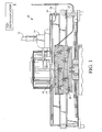
FIG. 1 shows a general schematic diagram of an existingprobe station 10 having guard and electromagnetic shield structures. A test signal is provided through atest path 12 to aprobe 14 havingprobe needles 16 that contact anelectrical device 18 resting upon achuck 20. The probe needles may alternatively be any type of contacts, such as for example, probe cards, probes on movable positioners, optical signals, and membrane probes. Thechuck 20 receives a guard signal through afirst transmission line 22 while a suspendedguard member 24 receives a guard signal through asecond transmission line 26. Thefirst transmission line 22 likewise includes a test signal path to thechuck 20. Thefirst transmission line 22, thetest path 12, theprobe 14, theneedles 16, thedevice 18, and thechuck 20 together form a large loop, as shown inFIG. 1 , to a common signal source at the test instrumentation. Normally within the probe station thetransmission line 22 is within a service loop that is several feet long to accommodate movement of thechuck 20. - The present inventors came to the realization that when using high current or pulsed tests, the large test loop that originates from the test equipment and passes through the chuck creates undesirable inductance. The inductance resulting from this large loop often interferes with test measurements, and in particular high current and/or pulsed signals. In addition, the
transmission line 22 is normally a small conductor which is not especially suitable for carrying high currents.FIG. 2 illustrates more schematically the resulting test loop for purposes of clarity. - The present inventors further determined that reducing or otherwise modifying this previously unrecognized source of inductance for high current and/or pulsed signals, namely, the inductive test loop could improve such measurements. The modification may include modifying or otherwise providing another test signal path from the
chuck 20 to the test instrumentation.FIG. 3 shows one embodiment of aprobe station 10 with a test loop having a decreased length. Rather than routing the test signal from thechuck 20 throughtransmission line 22, atransmission line 28 may interconnect thechuck 20 with the suspendedguard member 24, which is then electrically connected to the test instrumentation by anothertransmission line 29. The suspendedguard member 24 typically has its guard potential removed when performing this test. Accordingly, the suspendedguard member 24 is being used in a non-traditional manner, namely, not interconnected to a guard potential. The interconnection of thetransmission line 28 at thechuck 20 may be one of the layers of thechuck 20 such as the top layer of thechuck 20. The at least partially encirclingconductive member 33, normally connected to guard potential, may have a height greater than the top surface of the chuck, even with the top surface of the chuck, or below the top surface of the chuck. Preferably, there is an air gap between theconductive member 33 and thechuck 20. The air gap may be partially filled, substantially filled, or completely filled with dielectric material. The signal path to or from the top surface of the chuck may be provided through an opening in theconductive member 33. Electrically connecting thechuck 20 to the suspendedguard member 24 by thetransmission line 28, and to the test instrumentation bytransmission line 29, results in a smaller loop path than that provided by previously existing probe stations, as shown schematically inFIG. 4 . By reducing the length of the test path loop, electrical performance is improved, particularly when testing an electrical device using high-current and/or pulsed signals. - It is to be understood that the suspended plate may be suspended from above, typically using insulators, or supported by supports from within the probe station, or supported by the chuck or chuck assembly. Normally the suspended plate does not move together with the
chuck 20, but is rather maintained in a fixed spatial relationship with respect to theprobe station 10. Also, it is to be understood that the suspended plate may be any conductive member within the probe station that has the characteristic that it does not move together with thechuck 20, but is rather maintained in a fixed spatial relationship with respect to theprobe station 10. Alternatively, the suspended member may be any conductive member within the probe station that is free from being electrically connected to a guard and/or shield potential when used in the aforementioned configuration. - The interconnections from the
chuck 20 to the suspendedguard 24 is preferably totally within the environmental enclosure. A further explanation of the environmental enclosure is disclosed inU.S. Patent No. 5,457,398 . Interconnection within the environmental enclosure potentially reduces the length of the conductive path to less than it would have been had the interconnection been, at least in part, exterior to the environmental enclosure, or otherwise the test path passing from within the environmental enclosure to outside the environmental enclosure to within the environmental enclosure. - The
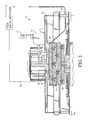
transmission lines FIGS. 2-4 may be embodied in many different structures. For example, thetransmission lines FIG. 5 , thetransmission line 28 may comprise a conductive shell orbowl 50 that contacts the test path of the chuck 20 (e.g., top layer) at its lower end and the suspendedplate 24 at its upper end. Theshell 50 preferably encircles a major portion of thechuck 20 and more preferably substantially all of thechuck 20. In addition, theshell 50 while preferably forming a substantially closed loop may have a size less than, at least in part, the exterior periphery defined by thechuck 20. Also, preferably theconductive shell 50 includes a flexible upper portion in contact with the suspended member so that upon pressing engagement a good conductive interconnection is made even while theconductive shell 50 moves horizontally relative to the suspendedplate 24. Moreover, theshell 50 may be detachably engageable with the suspended member by changing its height, such as for example, using "flip-up" fingers. In addition, a flexible upper portion also permits a greater range of movement of the chuck in the z-axis direction. In addition, the shell may be solid, flexible, and/or perforated with openings as desired. The openings, in particular, may be useful for permitting air flow around the device under test. - Referring to
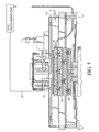
FIG. 6 , the reduced inductance test path may be included within the structure that includes anenclosure 37 that surrounds the chuck therein. During testing of the device under test theenclosure 37 moves together with thechuck 20. Theinterconnection 28 to the suspended member may be by a cable or otherwise from a location within the chamber or otherwise connected to the chuck therein. - Referring to
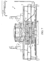
FIG. 7 , a dual probe assembly may be used to provide a test signal path. Afirst probe 70 may provide a test signal to the device under test. The test signal then passes through the device under test and to thechuck 20. Thechuck 20 is electrically interconnected to the suspendedplate 24. Asecond probe 72 may receive the test signal from the suspendedplate 24. Alternatively, thesecond probe 72 may be directly interconnected to thechuck 20 to receive the test signal. - Referring to
FIG. 8 , asingle probe assembly 80 may be used to provide and sense a test signal path. Theprobe 80 may provide a test signal to the device under test through afirst probe tip 82. The test signal then passes through the device under test and to thechuck 20. Thechuck 20 is electrically interconnected to the suspendedplate 24. Thesingle probe assembly 80 may receive the test signal from the suspendedplate 24 through asecond probe tip 84. Alternatively, the second tip of theprobe assembly 80 may be direct interconnection to thechuck 20 to receive the test signal. In this manner a single probe assembly may both provide the test signal and sense the test signal. Also, it is preferred that the interconnected from theprobe assembly 80 to the test instrumentation is a single cable assembly, more preferably a twisted pair of wires, to minimize inductance. The twisted pair of wires preferably extends at least 50% of the distance between the probe and the test instrumentation. - The terms and expressions employed in the foregoing specification are used therein as terms of description and not of limitation, it being recognized that the scope of the invention is defined and limited only by the claims that follow.
Claims (9)
- A probe assembly (10) for probing an electrical device (18), said probe assembly comprising:(a) a chuck (20) having a first conductive member with a support surface suitable for supporting an electrical device (18); and(b) a second conductive member (24) having a substantially planar surface spaced apart from, and opposed to, said support surface of said chuck (20), wherein said support surface is electrically interconnected to said second conductive member (24) and wherein said second conductive member is electrically interconnected to a test signal for said electrical device (18).
- The probe assembly (10) of claim 1 wherein said first conductive member comprises a first plate, said second conductive member (24) comprises a second plate, and wherein said second conductive member (24) is spaced further distant from said electrical device (18) than said first conductive member.
- The probe assembly (10) of claim 1 wherein said second conductive member (24) comprises a second plate and is vertically spaced apart from said first conductive member.
- The probe assembly (10) of claim 1 wherein said second conductive member (24) is electrically interconnected to said support surface completely within an environmental chamber.
- The probe assembly (10) of claim 1 wherein said second conductive member (24) is free from being supported by said chuck (20).
- The probe assembly (10) of claim 1 wherein said first conductive member is electrically interconnected to a first probe (70), wherein said second conductive member is electrically interconnected to a second probe (72).
- The probe assembly (10) of claim 1 wherein said first conductive member and said second conductive member (24) are electrically interconnected to a first probe (70).
- The probe assembly (10) of claim 1 wherein said first conductive member is electrically interconnected to a first probe (14, 70, 80) and wherein said first probe (14, 70, 80) is electrically interconnected to test instrumentation using a conductive element having a length, at least 50% of said length comprising a twisted pair of wires.
- The probe assembly (10) of claim 1 further comprising a detachable substantially closed loop member (28, 50) engageable with said first conductive member and said second conductive member, where said loop member (28, 50) includes a flexible member interconnecting said first conductive member and said second conductive member (24).
Priority Applications (1)
| Application Number | Priority Date | Filing Date | Title |
|---|---|---|---|
| DE20321019U DE20321019U1 (en) | 2002-11-25 | 2003-10-24 | Probe assembly for testing electrical device e.g. semiconductor wafer, has chuck with one conductive portion supporting electrical device, another portion spaced apart from chuck, and two portions interconnected to same potential |
Applications Claiming Priority (5)
| Application Number | Priority Date | Filing Date | Title |
|---|---|---|---|
| US42908202P | 2002-11-25 | 2002-11-25 | |
| US429082P | 2002-11-25 | ||
| US10/672,655 US7250779B2 (en) | 2002-11-25 | 2003-09-25 | Probe station with low inductance path |
| US672655 | 2003-09-25 | ||
| PCT/US2003/033767 WO2004049395A2 (en) | 2002-11-25 | 2003-10-24 | Probe station with low inductance path |
Publications (3)
| Publication Number | Publication Date |
|---|---|
| EP1567871A2 EP1567871A2 (en) | 2005-08-31 |
| EP1567871A4 EP1567871A4 (en) | 2006-05-17 |
| EP1567871B1 true EP1567871B1 (en) | 2012-03-21 |
Family
ID=32397172
Family Applications (1)
| Application Number | Title | Priority Date | Filing Date |
|---|---|---|---|
| EP03777879A Expired - Fee Related EP1567871B1 (en) | 2002-11-25 | 2003-10-24 | Probe station with low inductance path |
Country Status (6)
| Country | Link |
|---|---|
| US (2) | US7250779B2 (en) |
| EP (1) | EP1567871B1 (en) |
| JP (1) | JP4624262B2 (en) |
| KR (1) | KR20050086822A (en) |
| AU (1) | AU2003286669A1 (en) |
| WO (1) | WO2004049395A2 (en) |
Families Citing this family (30)
| Publication number | Priority date | Publication date | Assignee | Title |
|---|---|---|---|---|
| US5345170A (en) * | 1992-06-11 | 1994-09-06 | Cascade Microtech, Inc. | Wafer probe station having integrated guarding, Kelvin connection and shielding systems |
| US6445202B1 (en) | 1999-06-30 | 2002-09-03 | Cascade Microtech, Inc. | Probe station thermal chuck with shielding for capacitive current |
| US6965226B2 (en) * | 2000-09-05 | 2005-11-15 | Cascade Microtech, Inc. | Chuck for holding a device under test |
| US6914423B2 (en) | 2000-09-05 | 2005-07-05 | Cascade Microtech, Inc. | Probe station |
| US6836135B2 (en) * | 2001-08-31 | 2004-12-28 | Cascade Microtech, Inc. | Optical testing device |
| US7250779B2 (en) * | 2002-11-25 | 2007-07-31 | Cascade Microtech, Inc. | Probe station with low inductance path |
| US7221172B2 (en) * | 2003-05-06 | 2007-05-22 | Cascade Microtech, Inc. | Switched suspended conductor and connection |
| US7492172B2 (en) | 2003-05-23 | 2009-02-17 | Cascade Microtech, Inc. | Chuck for holding a device under test |
| JP4199629B2 (en) * | 2003-09-18 | 2008-12-17 | 株式会社日立ハイテクノロジーズ | Internal structure observation method and apparatus |
| US7250626B2 (en) | 2003-10-22 | 2007-07-31 | Cascade Microtech, Inc. | Probe testing structure |
| US7187188B2 (en) * | 2003-12-24 | 2007-03-06 | Cascade Microtech, Inc. | Chuck with integrated wafer support |
| US7656172B2 (en) | 2005-01-31 | 2010-02-02 | Cascade Microtech, Inc. | System for testing semiconductors |
| US7535247B2 (en) | 2005-01-31 | 2009-05-19 | Cascade Microtech, Inc. | Interface for testing semiconductors |
| US7652491B2 (en) * | 2006-11-17 | 2010-01-26 | Suss Microtec Test Systems Gmbh | Probe support with shield for the examination of test substrates under use of probe supports |
| US8130005B2 (en) * | 2006-12-14 | 2012-03-06 | Formfactor, Inc. | Electrical guard structures for protecting a signal trace from electrical interference |
| US7676953B2 (en) * | 2006-12-29 | 2010-03-16 | Signature Control Systems, Inc. | Calibration and metering methods for wood kiln moisture measurement |
| TWI434360B (en) * | 2008-09-04 | 2014-04-11 | Star Techn Inc | Enclosed type probe station |
| US8319503B2 (en) | 2008-11-24 | 2012-11-27 | Cascade Microtech, Inc. | Test apparatus for measuring a characteristic of a device under test |
| JP2012523920A (en) * | 2009-04-14 | 2012-10-11 | マウイ イマギング,インコーポレーテッド | Universal multi-aperture medical ultrasound probe |
| JP5296117B2 (en) * | 2010-03-12 | 2013-09-25 | 東京エレクトロン株式会社 | Probe device |
| JP5291157B2 (en) | 2011-08-01 | 2013-09-18 | 東京エレクトロン株式会社 | Probe card for power devices |
| JP5265746B2 (en) * | 2011-09-22 | 2013-08-14 | 東京エレクトロン株式会社 | Probe device |
| US9364925B2 (en) * | 2012-04-30 | 2016-06-14 | Globalfoundries Inc. | Assembly of electronic and optical devices |
| JP6042760B2 (en) * | 2013-03-28 | 2016-12-14 | 東京エレクトロン株式会社 | Probe device |
| KR101794744B1 (en) | 2013-08-14 | 2017-12-01 | 에프이아이 컴파니 | Circuit probe for charged particle beam system |
| US10281518B2 (en) | 2014-02-25 | 2019-05-07 | Formfactor Beaverton, Inc. | Systems and methods for on-wafer dynamic testing of electronic devices |
| US9989584B2 (en) * | 2014-07-11 | 2018-06-05 | Teradyne, Inc. | Controlling signal path inductance in automatic test equipment |
| US9784763B1 (en) | 2016-04-08 | 2017-10-10 | Cascade Microtech, Inc. | Shielded probe systems with controlled testing environments |
| JP7138463B2 (en) * | 2018-03-30 | 2022-09-16 | 株式会社日本マイクロニクス | prober |
| TWI738449B (en) | 2020-08-03 | 2021-09-01 | 致茂電子股份有限公司 | Wafer inspection system and wafer inspection equipment thereof |
Family Cites Families (205)
| Publication number | Priority date | Publication date | Assignee | Title |
|---|---|---|---|---|
| US1191486A (en) * | 1914-03-20 | 1916-07-18 | Edward B Tyler | Expansion-joint. |
| US1337866A (en) | 1917-09-27 | 1920-04-20 | Griffiths Ethel Grace | System for protecting electric cables |
| US2142625A (en) * | 1932-07-06 | 1939-01-03 | Hollandsche Draad En Kabelfab | High tension cable |
| US2197081A (en) | 1937-06-14 | 1940-04-16 | Transit Res Corp | Motor support |
| US2264685A (en) * | 1940-06-28 | 1941-12-02 | Westinghouse Electric & Mfg Co | Insulating structure |
| US2376101A (en) | 1942-04-01 | 1945-05-15 | Ferris Instr Corp | Electrical energy transmission |
| US2389668A (en) | 1943-03-04 | 1945-11-27 | Barnes Drill Co | Indexing mechanism for machine tables |
| US2471897A (en) | 1945-01-13 | 1949-05-31 | Trico Products Corp | Fluid motor packing |
| US2471697A (en) | 1946-11-08 | 1949-05-31 | Merck & Co Inc | Process for reducing carbonyl compounds to their corresponding methylene analogues |
| US2812502A (en) | 1953-07-07 | 1957-11-05 | Bell Telephone Labor Inc | Transposed coaxial conductor system |
| CH364040A (en) | 1960-04-19 | 1962-08-31 | Ipa Anstalt | Detection device to check if an element of an electrical installation is live |
| US3185927A (en) | 1961-01-31 | 1965-05-25 | Kulicke & Soffa Mfg Co | Probe instrument for inspecting semiconductor wafers including means for marking defective zones |
| US3193712A (en) | 1962-03-21 | 1965-07-06 | Clarence A Harris | High voltage cable |
| US3230299A (en) * | 1962-07-18 | 1966-01-18 | Gen Cable Corp | Electrical cable with chemically bonded rubber layers |
| US3256484A (en) | 1962-09-10 | 1966-06-14 | Tektronix Inc | High voltage test probe containing a part gas, part liquid dielectric fluid under pressure and having a transparent housing section for viewing the presence of the liquid therein |
| US3176091A (en) * | 1962-11-07 | 1965-03-30 | Helmer C Hanson | Controlled multiple switching unit |
| US3192844A (en) | 1963-03-05 | 1965-07-06 | Kulicke And Soffa Mfg Company | Mask alignment fixture |
| US3201721A (en) | 1963-12-30 | 1965-08-17 | Western Electric Co | Coaxial line to strip line connector |
| US3405361A (en) | 1964-01-08 | 1968-10-08 | Signetics Corp | Fluid actuable multi-point microprobe for semiconductors |
| US3289046A (en) | 1964-05-19 | 1966-11-29 | Gen Electric | Component chip mounted on substrate with heater pads therebetween |
| GB1069184A (en) * | 1965-04-15 | 1967-05-17 | Andre Rubber Co | Improvements in or relating to pipe couplings |
| US3333274A (en) | 1965-04-21 | 1967-07-25 | Micro Tech Mfg Inc | Testing device |
| US3435185A (en) * | 1966-01-11 | 1969-03-25 | Rohr Corp | Sliding vacuum seal for electron beam welder |
| US3408565A (en) | 1966-03-02 | 1968-10-29 | Philco Ford Corp | Apparatus for sequentially testing electrical components under controlled environmental conditions including a component support mating test head |
| US3484679A (en) | 1966-10-03 | 1969-12-16 | North American Rockwell | Electrical apparatus for changing the effective capacitance of a cable |
| FR1583782A (en) * | 1968-03-25 | 1969-12-05 | ||
| US3609539A (en) | 1968-09-28 | 1971-09-28 | Ibm | Self-aligning kelvin probe |
| NL6917791A (en) * | 1969-03-13 | 1970-09-15 | ||
| US3648169A (en) * | 1969-05-26 | 1972-03-07 | Teledyne Inc | Probe and head assembly |
| US3596228A (en) | 1969-05-29 | 1971-07-27 | Ibm | Fluid actuated contactor |
| US3602845A (en) | 1970-01-27 | 1971-08-31 | Us Army | Slot line nonreciprocal phase shifter |
| US3654573A (en) | 1970-06-29 | 1972-04-04 | Bell Telephone Labor Inc | Microwave transmission line termination |
| US3740900A (en) | 1970-07-01 | 1973-06-26 | Signetics Corp | Vacuum chuck assembly for semiconductor manufacture |
| US3642415A (en) * | 1970-08-10 | 1972-02-15 | Shell Oil Co | Plunger-and-diaphragm plastic sheet forming apparatus |
| US3700998A (en) | 1970-08-20 | 1972-10-24 | Computer Test Corp | Sample and hold circuit with switching isolation |
| US3714572A (en) * | 1970-08-21 | 1973-01-30 | Rca Corp | Alignment and test fixture apparatus |
| US4009456A (en) * | 1970-10-07 | 1977-02-22 | General Microwave Corporation | Variable microwave attenuator |
| US3662318A (en) | 1970-12-23 | 1972-05-09 | Comp Generale Electricite | Transition device between coaxial and microstrip lines |
| US3710251A (en) * | 1971-04-07 | 1973-01-09 | Collins Radio Co | Microelectric heat exchanger pedestal |
| US3814888A (en) | 1971-11-19 | 1974-06-04 | Gen Electric | Solid state induction cooking appliance |
| US3810017A (en) | 1972-05-15 | 1974-05-07 | Teledyne Inc | Precision probe for testing micro-electronic units |
| US3829076A (en) | 1972-06-08 | 1974-08-13 | H Sofy | Dial index machine |
| US3858212A (en) | 1972-08-29 | 1974-12-31 | L Tompkins | Multi-purpose information gathering and distribution system |
| US3952156A (en) | 1972-09-07 | 1976-04-20 | Xerox Corporation | Signal processing system |
| CA970849A (en) * | 1972-09-18 | 1975-07-08 | Malcolm P. Macmartin | Low leakage isolating transformer for electromedical apparatus |
| US3775644A (en) | 1972-09-20 | 1973-11-27 | Communications Satellite Corp | Adjustable microstrip substrate holder |
| US3777260A (en) | 1972-12-14 | 1973-12-04 | Ibm | Grid for making electrical contact |
| FR2298196A1 (en) | 1973-05-18 | 1976-08-13 | Lignes Telegraph Telephon | NON-RECIPROCAL COMPONENT WITH WIDE-BAND SLOT LINE |
| US3814838A (en) | 1973-06-01 | 1974-06-04 | Continental Electronics Mfg | Insulator assembly having load distribution support |
| US3930809A (en) * | 1973-08-21 | 1976-01-06 | Wentworth Laboratories, Inc. | Assembly fixture for fixed point probe card |
| US3863181A (en) * | 1973-12-03 | 1975-01-28 | Bell Telephone Labor Inc | Mode suppressor for strip transmission lines |
| US4001685A (en) * | 1974-03-04 | 1977-01-04 | Electroglas, Inc. | Micro-circuit test probe |
| US3936743A (en) * | 1974-03-05 | 1976-02-03 | Electroglas, Inc. | High speed precision chuck assembly |
| US3976959A (en) | 1974-07-22 | 1976-08-24 | Gaspari Russell A | Planar balun |
| US3970934A (en) | 1974-08-12 | 1976-07-20 | Akin Aksu | Printed circuit board testing means |
| US4042119A (en) | 1975-06-30 | 1977-08-16 | International Business Machines Corporation | Workpiece positioning apparatus |
| US4038894A (en) | 1975-07-18 | 1977-08-02 | Springfield Tool And Die, Inc. | Piercing apparatus |
| SE407115B (en) | 1975-10-06 | 1979-03-12 | Kabi Ab | PROCEDURES AND METAL ELECTRODES FOR THE STUDY OF ENZYMATIC AND OTHER BIOCHEMICAL REACTIONS |
| US4035723A (en) | 1975-10-16 | 1977-07-12 | Xynetics, Inc. | Probe arm |
| US3992073A (en) | 1975-11-24 | 1976-11-16 | Technical Wire Products, Inc. | Multi-conductor probe |
| US3996517A (en) | 1975-12-29 | 1976-12-07 | Monsanto Company | Apparatus for wafer probing having surface level sensing |
| US4116523A (en) | 1976-01-23 | 1978-09-26 | James M. Foster | High frequency probe |
| US4049252A (en) | 1976-02-04 | 1977-09-20 | Bell Theodore F | Index table |
| US4008900A (en) * | 1976-03-15 | 1977-02-22 | John Freedom | Indexing chuck |
| US4099120A (en) | 1976-04-19 | 1978-07-04 | Akin Aksu | Probe head for testing printed circuit boards |
| US4115735A (en) | 1976-10-14 | 1978-09-19 | Faultfinders, Inc. | Test fixture employing plural platens for advancing some or all of the probes of the test fixture |
| US4093988A (en) | 1976-11-08 | 1978-06-06 | General Electric Company | High speed frequency response measurement |
| US4186338A (en) * | 1976-12-16 | 1980-01-29 | Genrad, Inc. | Phase change detection method of and apparatus for current-tracing the location of faults on printed circuit boards and similar systems |
| US4115736A (en) | 1977-03-09 | 1978-09-19 | The United States Of America As Represented By The Secretary Of The Air Force | Probe station |
| US4151465A (en) | 1977-05-16 | 1979-04-24 | Lenz Seymour S | Variable flexure test probe for microelectronic circuits |
| US4161692A (en) | 1977-07-18 | 1979-07-17 | Cerprobe Corporation | Probe device for integrated circuit wafers |
| US4135131A (en) | 1977-10-14 | 1979-01-16 | The United States Of America As Represented By The Secretary Of The Army | Microwave time delay spectroscopic methods and apparatus for remote interrogation of biological targets |
| US4371742A (en) * | 1977-12-20 | 1983-02-01 | Graham Magnetics, Inc. | EMI-Suppression from transmission lines |
| US4172993A (en) | 1978-09-13 | 1979-10-30 | The Singer Company | Environmental hood for testing printed circuit cards |
| DE2849119A1 (en) | 1978-11-13 | 1980-05-14 | Siemens Ag | METHOD AND CIRCUIT FOR DAMPING MEASUREMENT, ESPECIALLY FOR DETERMINING THE DAMPING AND / OR GROUP DISTANCE DISTORTION OF A MEASURED OBJECT |
| US4383217A (en) | 1979-01-02 | 1983-05-10 | Shiell Thomas J | Collinear four-point probe head and mount for resistivity measurements |
| US4280112A (en) | 1979-02-21 | 1981-07-21 | Eisenhart Robert L | Electrical coupler |
| US4352061A (en) | 1979-05-24 | 1982-09-28 | Fairchild Camera & Instrument Corp. | Universal test fixture employing interchangeable wired personalizers |
| US4287473A (en) | 1979-05-25 | 1981-09-01 | The United States Of America As Represented By The United States Department Of Energy | Nondestructive method for detecting defects in photodetector and solar cell devices |
| US4277741A (en) | 1979-06-25 | 1981-07-07 | General Motors Corporation | Microwave acoustic spectrometer |
| JPS5933267B2 (en) | 1979-08-28 | 1984-08-14 | 三菱電機株式会社 | Failure analysis method for semiconductor devices |
| US4327180A (en) | 1979-09-14 | 1982-04-27 | Board Of Governors, Wayne State Univ. | Method and apparatus for electromagnetic radiation of biological material |
| US4284033A (en) | 1979-10-31 | 1981-08-18 | Rca Corporation | Means to orbit and rotate target wafers supported on planet member |
| US4330783A (en) | 1979-11-23 | 1982-05-18 | Toia Michael J | Coaxially fed dipole antenna |
| US4365195A (en) | 1979-12-27 | 1982-12-21 | Communications Satellite Corporation | Coplanar waveguide mounting structure and test fixture for microwave integrated circuits |
| US4365109A (en) | 1980-01-25 | 1982-12-21 | The United States Of America As Represented By The Secretary Of The Air Force | Coaxial cable design |
| US4342958A (en) | 1980-03-28 | 1982-08-03 | Honeywell Information Systems Inc. | Automatic test equipment test probe contact isolation detection method |
| JPS5953659B2 (en) | 1980-04-11 | 1984-12-26 | 株式会社日立製作所 | Reciprocating mechanism of rotating body in vacuum chamber |
| US4284682A (en) | 1980-04-30 | 1981-08-18 | Nasa | Heat sealable, flame and abrasion resistant coated fabric |
| US4357575A (en) | 1980-06-17 | 1982-11-02 | Dit-Mco International Corporation | Apparatus for use in testing printed circuit process boards having means for positioning such boards in proper juxtaposition with electrical contacting assemblies |
| US4346355A (en) | 1980-11-17 | 1982-08-24 | Raytheon Company | Radio frequency energy launcher |
| US4376920A (en) | 1981-04-01 | 1983-03-15 | Smith Kenneth L | Shielded radio frequency transmission cable |
| JPS57169244A (en) * | 1981-04-13 | 1982-10-18 | Canon Inc | Temperature controller for mask and wafer |
| US4414638A (en) | 1981-04-30 | 1983-11-08 | Dranetz Engineering Laboratories, Inc. | Sampling network analyzer with stored correction of gain errors |
| US4425395A (en) * | 1981-04-30 | 1984-01-10 | Fujikura Rubber Works, Ltd. | Base fabrics for polyurethane-coated fabrics, polyurethane-coated fabrics and processes for their production |
| US4401945A (en) | 1981-04-30 | 1983-08-30 | The Valeron Corporation | Apparatus for detecting the position of a probe relative to a workpiece |
| US4426619A (en) * | 1981-06-03 | 1984-01-17 | Temptronic Corporation | Electrical testing system including plastic window test chamber and method of using same |
| US4566184A (en) * | 1981-08-24 | 1986-01-28 | Rockwell International Corporation | Process for making a probe for high speed integrated circuits |
| US4419626A (en) | 1981-08-25 | 1983-12-06 | Daymarc Corporation | Broad band contactor assembly for testing integrated circuit devices |
| US4453142A (en) | 1981-11-02 | 1984-06-05 | Motorola Inc. | Microstrip to waveguide transition |
| US4480223A (en) | 1981-11-25 | 1984-10-30 | Seiichiro Aigo | Unitary probe assembly |
| US4528504A (en) | 1982-05-27 | 1985-07-09 | Harris Corporation | Pulsed linear integrated circuit tester |
| US4468629A (en) | 1982-05-27 | 1984-08-28 | Trw Inc. | NPN Operational amplifier |
| US4491173A (en) * | 1982-05-28 | 1985-01-01 | Temptronic Corporation | Rotatable inspection table |
| JPS58210631A (en) | 1982-05-31 | 1983-12-07 | Toshiba Corp | Ic tester utilizing electron beam |
| US4507602A (en) * | 1982-08-13 | 1985-03-26 | The United States Of America As Represented By The Secretary Of The Air Force | Measurement of permittivity and permeability of microwave materials |
| US4479690A (en) | 1982-09-13 | 1984-10-30 | The United States Of America As Represented By The Secretary Of The Navy | Underwater splice for submarine coaxial cable |
| US4487996A (en) | 1982-12-02 | 1984-12-11 | Electric Power Research Institute, Inc. | Shielded electrical cable |
| US4575676A (en) * | 1983-04-04 | 1986-03-11 | Advanced Research And Applications Corporation | Method and apparatus for radiation testing of electron devices |
| CH668646A5 (en) * | 1983-05-31 | 1989-01-13 | Contraves Ag | DEVICE FOR RECOVERING LIQUID VOLUME. |
| JPS59226167A (en) | 1983-06-04 | 1984-12-19 | Dainippon Screen Mfg Co Ltd | Surface treating device for circuit board |
| FR2547945B1 (en) | 1983-06-21 | 1986-05-02 | Raffinage Cie Francaise | NEW STRUCTURE OF ELECTRIC CABLE AND ITS APPLICATIONS |
| US4816767A (en) * | 1984-01-09 | 1989-03-28 | Hewlett-Packard Company | Vector network analyzer with integral processor |
| US4588970A (en) | 1984-01-09 | 1986-05-13 | Hewlett-Packard Company | Three section termination for an R.F. triaxial directional bridge |
| JPS60136006U (en) * | 1984-02-20 | 1985-09-10 | 株式会社 潤工社 | flat cable |
| US4557599A (en) | 1984-03-06 | 1985-12-10 | General Signal Corporation | Calibration and alignment target plate |
| US4646005A (en) * | 1984-03-16 | 1987-02-24 | Motorola, Inc. | Signal probe |
| JPS60235304A (en) | 1984-05-08 | 1985-11-22 | 株式会社フジクラ | Dc power cable |
| US4675600A (en) | 1984-05-17 | 1987-06-23 | Geo International Corporation | Testing apparatus for plated through-holes on printed circuit boards, and probe therefor |
| DE3428087A1 (en) * | 1984-07-30 | 1986-01-30 | Kraftwerk Union AG, 4330 Mülheim | CONCENTRIC THREE-WIRE CABLE |
| US4665360A (en) | 1985-03-11 | 1987-05-12 | Eaton Corporation | Docking apparatus |
| US4734872A (en) * | 1985-04-30 | 1988-03-29 | Temptronic Corporation | Temperature control for device under test |
| US4730158A (en) * | 1986-06-06 | 1988-03-08 | Santa Barbara Research Center | Electron-beam probing of photodiodes |
| US5095891A (en) * | 1986-07-10 | 1992-03-17 | Siemens Aktiengesellschaft | Connecting cable for use with a pulse generator and a shock wave generator |
| US4673839A (en) | 1986-09-08 | 1987-06-16 | Tektronix, Inc. | Piezoelectric pressure sensing apparatus for integrated circuit testing stations |
| US4904933A (en) * | 1986-09-08 | 1990-02-27 | Tektronix, Inc. | Integrated circuit probe station |
| US4812754A (en) * | 1987-01-07 | 1989-03-14 | Tracy Theodore A | Circuit board interfacing apparatus |
| US4727637A (en) * | 1987-01-20 | 1988-03-01 | The Boeing Company | Computer aided connector assembly method and apparatus |
| US4731577A (en) * | 1987-03-05 | 1988-03-15 | Logan John K | Coaxial probe card |
| US4810981A (en) * | 1987-06-04 | 1989-03-07 | General Microwave Corporation | Assembly of microwave components |
| US4894612A (en) * | 1987-08-13 | 1990-01-16 | Hypres, Incorporated | Soft probe for providing high speed on-wafer connections to a circuit |
| US5198752A (en) * | 1987-09-02 | 1993-03-30 | Tokyo Electron Limited | Electric probing-test machine having a cooling system |
| US5084671A (en) * | 1987-09-02 | 1992-01-28 | Tokyo Electron Limited | Electric probing-test machine having a cooling system |
| JP2554669Y2 (en) * | 1987-11-10 | 1997-11-17 | 博 寺町 | Rotary positioning device |
| US4896109A (en) * | 1987-12-07 | 1990-01-23 | The United States Of America As Represented By The Department Of Energy | Photoconductive circuit element reflectometer |
| US5091691A (en) * | 1988-03-21 | 1992-02-25 | Semitest, Inc. | Apparatus for making surface photovoltage measurements of a semiconductor |
| US4906920A (en) * | 1988-10-11 | 1990-03-06 | Hewlett-Packard Company | Self-leveling membrane probe |
| US4893914A (en) * | 1988-10-12 | 1990-01-16 | The Micromanipulator Company, Inc. | Test station |
| US4904935A (en) * | 1988-11-14 | 1990-02-27 | Eaton Corporation | Electrical circuit board text fixture having movable platens |
| US4982153A (en) * | 1989-02-06 | 1991-01-01 | Cray Research, Inc. | Method and apparatus for cooling an integrated circuit chip during testing |
| US5101149A (en) * | 1989-07-18 | 1992-03-31 | National Semiconductor Corporation | Modifiable IC board |
| US5097207A (en) * | 1989-11-03 | 1992-03-17 | John H. Blanz Company, Inc. | Temperature stable cryogenic probe station |
| US5089774A (en) * | 1989-12-26 | 1992-02-18 | Sharp Kabushiki Kaisha | Apparatus and a method for checking a semiconductor |
| JPH03209737A (en) * | 1990-01-11 | 1991-09-12 | Tokyo Electron Ltd | Probe equipment |
| US5001423A (en) * | 1990-01-24 | 1991-03-19 | International Business Machines Corporation | Dry interface thermal chuck temperature control system for semiconductor wafer testing |
| US4994737A (en) * | 1990-03-09 | 1991-02-19 | Cascade Microtech, Inc. | System for facilitating planar probe measurements of high-speed interconnect structures |
| US5198753A (en) * | 1990-06-29 | 1993-03-30 | Digital Equipment Corporation | Integrated circuit test fixture and method |
| JP2802825B2 (en) * | 1990-09-22 | 1998-09-24 | 大日本スクリーン製造 株式会社 | Semiconductor wafer electrical measurement device |
| US5094536A (en) * | 1990-11-05 | 1992-03-10 | Litel Instruments | Deformable wafer chuck |
| DE69130205T2 (en) * | 1990-12-25 | 1999-03-25 | Ngk Insulators Ltd | Semiconductor wafer heater and method of manufacturing the same |
| JPH05136218A (en) * | 1991-02-19 | 1993-06-01 | Tokyo Electron Yamanashi Kk | Inspection device |
| US5101453A (en) * | 1991-07-05 | 1992-03-31 | Cascade Microtech, Inc. | Fiber optic wafer probe |
| US5198756A (en) * | 1991-07-29 | 1993-03-30 | Atg-Electronics Inc. | Test fixture wiring integrity verification device |
| US5198758A (en) * | 1991-09-23 | 1993-03-30 | Digital Equipment Corp. | Method and apparatus for complete functional testing of a complex signal path of a semiconductor chip |
| US5345170A (en) * | 1992-06-11 | 1994-09-06 | Cascade Microtech, Inc. | Wafer probe station having integrated guarding, Kelvin connection and shielding systems |
| FR2695508B1 (en) * | 1992-09-08 | 1994-10-21 | Filotex Sa | Low noise cable. |
| US5382898A (en) * | 1992-09-21 | 1995-01-17 | Cerprobe Corporation | High density probe card for testing electrical circuits |
| US5684669A (en) * | 1995-06-07 | 1997-11-04 | Applied Materials, Inc. | Method for dechucking a workpiece from an electrostatic chuck |
| JPH0714898A (en) * | 1993-06-23 | 1995-01-17 | Mitsubishi Electric Corp | Equipment and method for testing and analyzing semiconductor wafer |
| JP2673870B2 (en) * | 1993-06-25 | 1997-11-05 | 株式会社日本マイクロニクス | Electric circuit measuring device |
| JP3346838B2 (en) * | 1993-06-29 | 2002-11-18 | 有限会社創造庵 | Rotary movement mechanism |
| JP3442822B2 (en) * | 1993-07-28 | 2003-09-02 | アジレント・テクノロジー株式会社 | Measurement cable and measurement system |
| US5594358A (en) * | 1993-09-02 | 1997-01-14 | Matsushita Electric Industrial Co., Ltd. | Radio frequency probe and probe card including a signal needle and grounding needle coupled to a microstrip transmission line |
| US5500606A (en) * | 1993-09-16 | 1996-03-19 | Compaq Computer Corporation | Completely wireless dual-access test fixture |
| US5486975A (en) * | 1994-01-31 | 1996-01-23 | Applied Materials, Inc. | Corrosion resistant electrostatic chuck |
| US5491426A (en) * | 1994-06-30 | 1996-02-13 | Vlsi Technology, Inc. | Adaptable wafer probe assembly for testing ICs with different power/ground bond pad configurations |
| US5488954A (en) * | 1994-09-09 | 1996-02-06 | Georgia Tech Research Corp. | Ultrasonic transducer and method for using same |
| US5835997A (en) * | 1995-03-28 | 1998-11-10 | University Of South Florida | Wafer shielding chamber for probe station |
| US5561377A (en) * | 1995-04-14 | 1996-10-01 | Cascade Microtech, Inc. | System for evaluating probing networks |
| KR0176434B1 (en) * | 1995-10-27 | 1999-04-15 | 이대원 | Vacuum chuck apparatus |
| US5712571A (en) * | 1995-11-03 | 1998-01-27 | Analog Devices, Inc. | Apparatus and method for detecting defects arising as a result of integrated circuit processing |
| US5861743A (en) * | 1995-12-21 | 1999-01-19 | Genrad, Inc. | Hybrid scanner for use in an improved MDA tester |
| JP2900877B2 (en) * | 1996-03-22 | 1999-06-02 | 日本電気株式会社 | Semiconductor device wiring current observation method, wiring system defect inspection method, and apparatus therefor |
| US6023209A (en) * | 1996-07-05 | 2000-02-08 | Endgate Corporation | Coplanar microwave circuit having suppression of undesired modes |
| US5963027A (en) * | 1997-06-06 | 1999-10-05 | Cascade Microtech, Inc. | Probe station having environment control chambers with orthogonally flexible lateral wall assembly |
| US6002263A (en) * | 1997-06-06 | 1999-12-14 | Cascade Microtech, Inc. | Probe station having inner and outer shielding |
| US6029141A (en) * | 1997-06-27 | 2000-02-22 | Amazon.Com, Inc. | Internet-based customer referral system |
| WO1999004273A1 (en) * | 1997-07-15 | 1999-01-28 | Wentworth Laboratories, Inc. | Probe station with multiple adjustable probe supports |
| US6013586A (en) * | 1997-10-09 | 2000-01-11 | Dimension Polyant Sailcloth, Inc. | Tent material product and method of making tent material product |
| US6229322B1 (en) * | 1998-08-21 | 2001-05-08 | Micron Technology, Inc. | Electronic device workpiece processing apparatus and method of communicating signals within an electronic device workpiece processing apparatus |
| JP2000183120A (en) * | 1998-12-17 | 2000-06-30 | Mitsubishi Electric Corp | Prober device and electrical evaluation method for semiconductor device |
| JP2000180469A (en) * | 1998-12-18 | 2000-06-30 | Fujitsu Ltd | Contactor for semiconductor device, tester using contactor for semiconductor device, testing method using contactor for semiconductor device and method for cleaning contactor for semiconductor device |
| JP3388462B2 (en) * | 1999-09-13 | 2003-03-24 | 日本電気株式会社 | Semiconductor chip analysis prober and semiconductor chip analysis device |
| US6313567B1 (en) * | 2000-04-10 | 2001-11-06 | Motorola, Inc. | Lithography chuck having piezoelectric elements, and method |
| US6650135B1 (en) * | 2000-06-29 | 2003-11-18 | Motorola, Inc. | Measurement chuck having piezoelectric elements and method |
| US6424141B1 (en) * | 2000-07-13 | 2002-07-23 | The Micromanipulator Company, Inc. | Wafer probe station |
| GB0021975D0 (en) * | 2000-09-07 | 2000-10-25 | Optomed As | Filter optic probes |
| WO2002052285A1 (en) * | 2000-12-22 | 2002-07-04 | Tokyo Electron Limited | Probe cartridge assembly and multi-probe assembly |
| US7006046B2 (en) * | 2001-02-15 | 2006-02-28 | Integral Technologies, Inc. | Low cost electronic probe devices manufactured from conductive loaded resin-based materials |
| JP4029603B2 (en) * | 2001-05-31 | 2008-01-09 | 豊田合成株式会社 | Weather strip |
| US7071714B2 (en) * | 2001-11-02 | 2006-07-04 | Formfactor, Inc. | Method and system for compensating for thermally induced motion of probe cards |
| US6777964B2 (en) * | 2002-01-25 | 2004-08-17 | Cascade Microtech, Inc. | Probe station |
| US6806697B2 (en) * | 2002-04-05 | 2004-10-19 | Agilent Technologies, Inc. | Apparatus and method for canceling DC errors and noise generated by ground shield current in a probe |
| US6856129B2 (en) * | 2002-07-09 | 2005-02-15 | Intel Corporation | Current probe device having an integrated amplifier |
| JP4043339B2 (en) * | 2002-10-22 | 2008-02-06 | 川崎マイクロエレクトロニクス株式会社 | Test method and test apparatus |
| US6847219B1 (en) * | 2002-11-08 | 2005-01-25 | Cascade Microtech, Inc. | Probe station with low noise characteristics |
| US6724205B1 (en) * | 2002-11-13 | 2004-04-20 | Cascade Microtech, Inc. | Probe for combined signals |
| US7250779B2 (en) * | 2002-11-25 | 2007-07-31 | Cascade Microtech, Inc. | Probe station with low inductance path |
| US6861856B2 (en) * | 2002-12-13 | 2005-03-01 | Cascade Microtech, Inc. | Guarded tub enclosure |
| US6838885B2 (en) * | 2003-03-05 | 2005-01-04 | Murata Manufacturing Co., Ltd. | Method of correcting measurement error and electronic component characteristic measurement apparatus |
| US7002133B2 (en) * | 2003-04-11 | 2006-02-21 | Hewlett-Packard Development Company, L.P. | Detecting one or more photons from their interactions with probe photons in a matter system |
| US7221172B2 (en) * | 2003-05-06 | 2007-05-22 | Cascade Microtech, Inc. | Switched suspended conductor and connection |
| KR100523139B1 (en) * | 2003-06-23 | 2005-10-20 | 주식회사 하이닉스반도체 | Semiconductor device for reducing the number of probing pad used during wafer testing and method for testing the same |
| US7001785B1 (en) * | 2004-12-06 | 2006-02-21 | Veeco Instruments, Inc. | Capacitance probe for thin dielectric film characterization |
| US7005879B1 (en) * | 2005-03-01 | 2006-02-28 | International Business Machines Corporation | Device for probe card power bus noise reduction |
-
2003
- 2003-09-25 US US10/672,655 patent/US7250779B2/en not_active Expired - Lifetime
- 2003-10-24 WO PCT/US2003/033767 patent/WO2004049395A2/en active Application Filing
- 2003-10-24 JP JP2005510352A patent/JP4624262B2/en not_active Expired - Fee Related
- 2003-10-24 KR KR1020057009430A patent/KR20050086822A/en not_active Application Discontinuation
- 2003-10-24 AU AU2003286669A patent/AU2003286669A1/en not_active Abandoned
- 2003-10-24 EP EP03777879A patent/EP1567871B1/en not_active Expired - Fee Related
-
2007
- 2007-06-20 US US11/820,518 patent/US7498828B2/en not_active Expired - Fee Related
Also Published As
| Publication number | Publication date |
|---|---|
| JP2006507694A (en) | 2006-03-02 |
| US7250779B2 (en) | 2007-07-31 |
| AU2003286669A8 (en) | 2004-06-18 |
| KR20050086822A (en) | 2005-08-30 |
| AU2003286669A1 (en) | 2004-06-18 |
| US20070247178A1 (en) | 2007-10-25 |
| JP4624262B2 (en) | 2011-02-02 |
| EP1567871A4 (en) | 2006-05-17 |
| WO2004049395A2 (en) | 2004-06-10 |
| US20050099192A1 (en) | 2005-05-12 |
| US7498828B2 (en) | 2009-03-03 |
| WO2004049395A3 (en) | 2005-01-20 |
| EP1567871A2 (en) | 2005-08-31 |
Similar Documents
| Publication | Publication Date | Title |
|---|---|---|
| EP1567871B1 (en) | Probe station with low inductance path | |
| US6124723A (en) | Probe holder for low voltage, low current measurements in a water probe station | |
| US7138810B2 (en) | Probe station with low noise characteristics | |
| US7468609B2 (en) | Switched suspended conductor and connection | |
| Wiggins et al. | Transient electromagnetic interference in substations | |
| JP4195124B2 (en) | Probing method for probe station and test apparatus | |
| KR100273173B1 (en) | Impedance controlled interconnection device | |
| US20070252606A1 (en) | Shielded Probe Apparatus for Probing Semiconductor Wafer | |
| KR19980043156A (en) | Low Current Test Card | |
| US20050253612A1 (en) | Apparatus and method for terminating probe apparatus of semiconductor wafer | |
| KR20020018027A (en) | A method and device for detecting a partial discharge in an electrical device | |
| US5486770A (en) | High frequency wafer probe apparatus and method | |
| KR100396129B1 (en) | Electromechanical switching device package with controlled impedance environment | |
| US5825190A (en) | Method and apparatus for measuring a transfer impedance of shielded devices and common mode currents in shieldings | |
| JP2673870B2 (en) | Electric circuit measuring device | |
| KR20180079934A (en) | Vertical ultra-low leakage current probe card for dc parameter test | |
| KR102489319B1 (en) | Connector for electrical connection | |
| JP2005149854A (en) | Probe, ic socket, and semiconductor circuit | |
| US20030062914A1 (en) | Surface mating compliant contact assembly with fixed signal path length | |
| JPS5851482A (en) | Socket for semiconductor device | |
| KR20190105985A (en) | Test Socket Of Semiconductor Device | |
| KR101481876B1 (en) | Low noise connector and adapter for probe station | |
| WO1999004276A1 (en) | Probe station with emi shielding | |
| KR20010083382A (en) | Standard fields generation cell for emc testing and calibration | |
| JP2002100657A (en) | Semiconductor measuring apparatus |
Legal Events
| Date | Code | Title | Description |
|---|---|---|---|
| PUAI | Public reference made under article 153(3) epc to a published international application that has entered the european phase |
Free format text: ORIGINAL CODE: 0009012 |
|
| 17P | Request for examination filed |
Effective date: 20050617 |
|
| AK | Designated contracting states |
Kind code of ref document: A2 Designated state(s): AT BE BG CH CY CZ DE DK EE ES FI FR GB GR HU IE IT LI LU MC NL PT RO SE SI SK TR |
|
| AX | Request for extension of the european patent |
Extension state: AL LT LV MK |
|
| DAX | Request for extension of the european patent (deleted) | ||
| RBV | Designated contracting states (corrected) |
Designated state(s): DE FR GB |
|
| A4 | Supplementary search report drawn up and despatched |
Effective date: 20060403 |
|
| 17Q | First examination report despatched |
Effective date: 20100301 |
|
| REG | Reference to a national code |
Ref country code: DE Ref legal event code: R079 Ref document number: 60340370 Country of ref document: DE Free format text: PREVIOUS MAIN CLASS: G01R0031020000 Ipc: G01R0031280000 |
|
| GRAP | Despatch of communication of intention to grant a patent |
Free format text: ORIGINAL CODE: EPIDOSNIGR1 |
|
| RIC1 | Information provided on ipc code assigned before grant |
Ipc: G01R 31/28 20060101AFI20110907BHEP |
|
| GRAS | Grant fee paid |
Free format text: ORIGINAL CODE: EPIDOSNIGR3 |
|
| GRAA | (expected) grant |
Free format text: ORIGINAL CODE: 0009210 |
|
| AK | Designated contracting states |
Kind code of ref document: B1 Designated state(s): DE FR GB |
|
| REG | Reference to a national code |
Ref country code: GB Ref legal event code: FG4D |
|
| REG | Reference to a national code |
Ref country code: DE Ref legal event code: R096 Ref document number: 60340370 Country of ref document: DE Effective date: 20120516 |
|
| RAP2 | Party data changed (patent owner data changed or rights of a patent transferred) |
Owner name: CASCADE MICROTECH, INC. |
|
| PLBE | No opposition filed within time limit |
Free format text: ORIGINAL CODE: 0009261 |
|
| STAA | Information on the status of an ep patent application or granted ep patent |
Free format text: STATUS: NO OPPOSITION FILED WITHIN TIME LIMIT |
|
| 26N | No opposition filed |
Effective date: 20130102 |
|
| REG | Reference to a national code |
Ref country code: DE Ref legal event code: R097 Ref document number: 60340370 Country of ref document: DE Effective date: 20130102 |
|
| GBPC | Gb: european patent ceased through non-payment of renewal fee |
Effective date: 20121024 |
|
| PG25 | Lapsed in a contracting state [announced via postgrant information from national office to epo] |
Ref country code: GB Free format text: LAPSE BECAUSE OF NON-PAYMENT OF DUE FEES Effective date: 20121024 |
|
| REG | Reference to a national code |
Ref country code: FR Ref legal event code: PLFP Year of fee payment: 13 |
|
| REG | Reference to a national code |
Ref country code: FR Ref legal event code: PLFP Year of fee payment: 14 |
|
| REG | Reference to a national code |
Ref country code: FR Ref legal event code: PLFP Year of fee payment: 15 |
|
| REG | Reference to a national code |
Ref country code: FR Ref legal event code: PLFP Year of fee payment: 16 |
|
| PGFP | Annual fee paid to national office [announced via postgrant information from national office to epo] |
Ref country code: FR Payment date: 20181025 Year of fee payment: 16 |
|
| PGFP | Annual fee paid to national office [announced via postgrant information from national office to epo] |
Ref country code: DE Payment date: 20191206 Year of fee payment: 17 |
|
| PG25 | Lapsed in a contracting state [announced via postgrant information from national office to epo] |
Ref country code: FR Free format text: LAPSE BECAUSE OF NON-PAYMENT OF DUE FEES Effective date: 20191031 |
|
| REG | Reference to a national code |
Ref country code: DE Ref legal event code: R119 Ref document number: 60340370 Country of ref document: DE |
|
| PG25 | Lapsed in a contracting state [announced via postgrant information from national office to epo] |
Ref country code: DE Free format text: LAPSE BECAUSE OF NON-PAYMENT OF DUE FEES Effective date: 20210501 |