BACKGROUND
-
Positioning devices may be employed in applications of varying scale, such as in
microscopy (e.g., scanning probe microscopy), micro-assembly, and nano-assembly.
Positioning devices may also be employed in applications of varying function, such as for
probing, characterization, imaging and testing, as well as for manipulation and assembly.
-
Such positioning devices may be employed where it is necessary for a subject piece
being examined or assembled to be coarsely positioned on a larger scale, such as to move the
subject generally into place, and then finely positioned on a smaller scale to complete
examination or assembly. Moreover, fine positioning can be critical to manipulation and
examination of small-scale assemblers, probes, and scanning microscopes. For example, on
very small scales, vibrations that may be caused by traditional coarse positioning devices can
become intolerable. Nonetheless, it is often desirable or necessary for coarse positioning and
fine positioning to be available on the same device.
-
The terms "micro-electronic device" and "micro-assembly" are employed generically
herein to encompass micro-electronic components, micro-mechanical components, micro-electro-mechanical
components, MEMs components and assemblies thereof. Generally,
micro-electronic devices have feature dimensions that are less than about 1000 microns. The
present disclosure also relates to nano-electronic devices, including nano-electro-mechanical
devices (NEMs), which may have feature dimensions that are less than about 10 microns.
Macro-scale electronic devices may also be used to generate movements on a microscopic
scale and are also within the scope of the present disclosure. Macro-scale devices generally
have feature dimensions that are larger than about 1000 microns, although 1000 microns is
not an absolute demarcation between micro-scale and macro-scale devices.
BRIEF DESCRIPTION OF THE DRAWINGS
-
The present disclosure is best understood from the following detailed description
when read with the accompanying figures. It is emphasized that, in accordance with the
standard practice in the industry, various features are not drawn to scale. In fact, the
dimensions of the various features may be arbitrarily increased or reduced for clarity of
discussion.
-
Fig. 1a is a perspective view of at least a portion of one embodiment of an apparatus
according to aspects of the present disclosure.
-
Fig. 1b is a perspective view of at least a portion of one embodiment of an apparatus
according to aspects of the present disclosure.
-
Fig. 2 is a sectional view of at least a portion of one embodiment of an apparatus
according to aspects of the present disclosure.
-
Fig. 3 is a sectional view of at least a portion of one embodiment of an apparatus
according to aspects of the present disclosure.
-
Fig. 4 is a sectional view of at least a portion of one embodiment of an apparatus
according to aspects of the present disclosure.
-
Fig. 5 is a perspective view of at least a portion of one embodiment of an apparatus
according to aspects of the present disclosure.
-
Fig. 6 is a perspective view of at least a portion of one embodiment of an apparatus
according to aspects of the present disclosure.
-
Fig. 7 is a perspective view of at least a portion of one embodiment of an apparatus
according to aspects of the present disclosure.
-
Fig. 8 is a cutaway perspective view of at least a portion of one embodiment of an
apparatus according to aspects of the present disclosure.
-
Fig. 9 is a perspective view of at least a portion of one embodiment of an apparatus
according to aspects of the present disclosure.
-
Fig. 10 is a side view of at least a portion of one embodiment of an apparatus
according to aspects of the present disclosure.
-
Fig. 11 is a perspective view of at least a portion of one embodiment of an apparatus
according to aspects of the present disclosure.
-
Fig. 12 is a perspective view of at least a portion of one embodiment of an apparatus
according to aspects of the present disclosure.
-
Fig. 13 is a perspective view of at least a portion of one embodiment of an apparatus
according to aspects of the present disclosure.
-
Fig. 14 is a perspective view of at least a portion of one embodiment of an apparatus
according to aspects of the present disclosure.
DETAILED DESCRIPTION
-
It is to be understood that the following disclosure provides many different
embodiments, or examples, for implementing different features of various embodiments.
Specific examples of components and arrangements are described below to simplify the
present disclosure. These are, of course, merely examples and are not intended to be limiting.
In addition, the present disclosure may repeat reference numerals and/or letters in the various
examples. This repetition is for the purpose of simplicity and clarity and does not, in itself,
dictate a relationship between the various embodiments and/or configurations discussed.
Moreover, the formation of a first feature over or on a second feature in the description that
follows may include embodiments in which the first and second features are formed in direct
contact, and may also include embodiments in which additional features may be formed
interposing the first and second features, such that the first and second features may not be in
direct contact.
-
Referring to Fig. 1a, illustrated is a perspective view of at least a portion of one
embodiment of an apparatus 100 according to aspects of the present disclosure. The
apparatus 100 may be, include, or comprise a portion of an electro-mechanical device, a
micro-electro-mechanical device (e.g., a MEMS device), a microelectronic device or other
device within the scope of the present disclosure.
-
The apparatus 100 includes a base 110, which may comprise plastic, metal, silicon,
and/or other materials. The base 110 may be manufactured by casting, molding, machining,
ion beam milling, and/or other methods. The thickness of the base 110 may range from about
0.1 millimeters to about 1 millimeter, the length of the base 110 may range from about 5
millimeters to about 20 millimeters, and the width may range from about 2.5 millimeters to
about 5 millimeters. In other embodiments, thickness of the base 110 may range between
about 0.1 microns and about 5 microns, the length may range between about 50 microns and
about 200 microns, and the width may range between about 25 microns and about 50
microns. Other ranges are possible that may be outside of those given. The present
disclosure is not meant to be limited by ranges given herein.
-
An insulator 130 may be employed to attach an end 151 of a piezoelectric element
150 to the base 110. The insulator 130 may comprise glass, silicon oxide, and/or other
dielectric materials. The insulator 130 may be formed by cutting, grinding, casting,
machining, electro-discharge machining (EDM), and/or other methods, possibly to a
thickness ranging from about 0.1 millimeter to about 1 millimeter. In other embodiments, the
insulator 130 may be manufactured or otherwise formed on or over the base 110 by chemical
vapor deposition (CVD), physical vapor deposition (PVD), plasma enhanced CVD (PECVD),
atomic layer deposition (ALD), and/or other processes, possibly to a thickness ranging
between about 0.1 microns and about 5 microns.
-
In some embodiments, the insulator 130 may be optional. For example, a portion or
layer of the base 110 may comprise a dielectric material, such that the end 151 of the
piezoelectric element 150 may be attached directly to the base 110. The piezoelectric
element 150 and the base 110 may also be electrically and/or physically separated by features
other than the insulator 130.
-
The piezoelectric element 150 may be generally reed-shaped. For example, the
piezoelectric element 150 may have a substantially rectilinear shape having a width
substantially greater than a thickness and a length substantially greater than the width, such
that a cross-section substantially orthogonal to any axis of the piezoelectric element 150 may
be substantially rectangular. However, other configurations are possible. For example, the
piezoelectric element 150 may also have a circular cross-section, or perhaps a rounded but
non-circular cross-section such as that which would reduce rotation of the piezoelectric
element 150 relative to the base 110 or other proximate component. The cross-section of the
piezoelectric element 150 may also vary in size and/or shape along its length.
-
The piezoelectric element 150 may comprise piezoelectric materials such as, for
example, lead zirconate titanate (PZT), lead titanate (PbTiO3), lead metaniobate (PbNb2O6),
polyviylidene-fluoride (PVDF), zinc oxide (ZnO), polyviylidene-fluoride-triflourethylene
(PVDF-TrFE), and/or other materials. The piezoelectric element 150 may be formed by
sintering, grinding, and/or other processes. The piezoelectric element 150 may also be
polarized. For example, the piezoelectric element 150 may be polarized by being heated
(e.g., to above the curie point) and having an electric and/or magnetic field applied, and/or by
other methods.
-
The piezoelectric element 150 may have thickness ranging between about 0.1
millimeters and about 1 millimeter. The length may range between about 0.5 centimeters and
about 15 centimeters and the width may range between about 2.5 millimeters and about 5
centimeters. In other embodiments, the piezoelectric element 150 may have a thickness
ranging from about 0.1 microns to about 5 microns, a width ranging from about 25 microns to
about 50 microns, and a length ranging from about 50 microns to about 200 microns.
-
The piezoelectric element 150 may respond to an electrical signal by elongating
and/or constricting. A periodic or otherwise fluctuating electrical signal or wave may be
applied to the piezoelectric element 150 to achieve coarse positioning with the apparatus 100,
while a non-fluctuating electrical signal may be employed to achieve fine positioning using
the same piezoelectric element. In some embodiments, the piezoelectric element 150 may
respond to either electrical signal by bending, in addition to or in the alternative to elongation
and/or constriction.
-
A friction element 170 may be coupled to an end 156 of the piezoelectric element 150
distal from the insulator 130, such as to take full advantage of the motion of the piezoelectric
element 150. The friction element 170 may comprise aluminum-bronze, phosphor-bronze,
copper-beryllium, copper alloys, sapphire, and/or other materials, and may be formed by
electro-chemical machining (ECM), electrical discharge machining (EDM), milling, and/or
other methods. In one embodiment, the friction element 170 may be a boss extending from
the piezoelectric element 150 wherein such an extension may be integrated with, or coupled
to, the piezoelectric element 150.
-
In one embodiment, the thickness of the friction element 170 may range between
about 0.1 millimeters and about 1 millimeter, and the diameter may range between about 0.8
millimeters and about 5 millimeters. The diameter may range between about 8 microns and
about 50 microns. In other embodiments, the thickness of the friction element 170 may range
between about 0.1 microns and about 5 microns.
-
The shape of the friction element 170 may be substantially cylindrical. In other
embodiments, the friction element 170 may have other shapes or configurations, such as
polyhedral shapes. The friction element 170 may also have a substantially square or
rectangular footprint relative to the piezoelectric element 150. The friction element 170 may
also comprise multiple friction members arranged in various configurations on the
piezoelectric element 150. For example, Fig. 1b illustrates a perspective view of another
embodiment of the friction element 170, designated by reference number 170a, according to
aspects of the present disclosure. The friction element 170a includes a central section 171
which may have means (e.g., a fastener hole 172) for attachment to an piezoelectric element
150 (Fig. 1a). Supports 174a-d, which may be springs or otherwise resilient and/or flexible
members or portions, support friction members 175a-d, respectively. The friction members
175a-d, and possibly a substantial portion of the entire friction element 170a, may be
substantially similar to the friction element 170 (Fig. 1a) in composition, manufacture, and/or
otherwise.
-
As shown in Fig. 1a, the friction element 170 selectively frictionally engages a driven
element 190. The driven element 190 may be guided or restricted in one or more degrees of
freedom (e.g., its planes of movement) by the base 110. For example, the base 110 may
restrict predetermined degrees or directions of translation and/or rotation of the driven
element 190 by employing a friction slide or a rolling element bearing slide configuration.
Accordingly, motion of the driven element 190 may be limited to one degree of freedom,
although other embodiments may allow more degrees of freedom. The driven element 190
may hold or convey an object or specimen 199 that is being moved by the apparatus 100. For
example, the object 199 may be a micro-component or nano-device being assembled, or a
specimen being scanned by a scanning electron microscope (SEM), other charged particle
apparatus, or other types of microscopes. In some embodiments, the apparatus 100 includes
attachment means for retaining the specimen 199 on the surface of the driven element 190.
For example, the driven element 190 may include a recess or groove configured to receive the
specimen 199, or a snap-type or friction connector may secure the test specimen 199 to the
driven element 190.
-
The movement of the driven element 190 may be achieved by applying an electrical
signal to the piezoelectric element 150, which may cause the piezoelectric element to
elongate or contract. The friction element 170, or the piezoelectric element 150 itself, may
transfer some, all, or a portion of, such movement to the driven element 190 based on the
frequency, amplitude, and/or shape of the electrical signal. For example, to achieve coarse
positioning with the apparatus 100, a voltage waveform may be applied to the piezoelectric
element 150. Examples of voltage waveforms may include, but are not limited to, square
waves, saw-tooth waves, cycloidal waves, parabolic waves, and/or superimpositions or
combinations thereof.
-
For example, in embodiments in which a saw-tooth voltage waveform is applied, the
piezoelectric element 150 may elongate or contract according to its bias or polarity. During
the relatively shallow phase of the waveform, the piezoelectric element 150 (or the friction
element 170) may "stick" to the driven element 190 for a substantial portion of the shallow
phase such that most or all of the movement of the piezoelectric element is transferred to the
driven element 190. However, during the relatively steep phase of the waveform, the
elongation/contraction of the piezoelectric element 150 will be correspondingly faster and
may cause the piezoelectric element 150 (or friction element 170) to overcome the static
friction against the driven element 190 and "slip" during a substantial portion of the steep
phase such that little or no movement of the piezoelectric element 190 may be transferred to
the driven element 190. When the shallower phase of the waveform returns, the
elongation/contraction of the piezoelectric element 150 may once again impart movement to
the driven element 190. Thus the friction element 170 may selectively and frictionally
engages the driven element 190 as a function of velocity, acceleration and/or friction
coefficient of the friction element 170 relative to the driven element 190. This may be
referred to as "slip-stick" or "stick-slip" motion.
-
The frequency of the waveform may vary and, in some embodiments, ranges between
about 1 Hz and about 1 kHz. The amplitude of the waveform may also vary and, in some
embodiments, ranges between about 2 V and about 500 V. Following the coarse positioning
by slip-stick movement, a direct voltage may be applied to finely position the driven element
190 and, in turn, the object or specimen 199 positioned thereto. The direct voltage may range
between about 10 mV and about 1 kV.
-
In other embodiments, the frequency, amplitude, and direct voltage may vary. For
example, the wave form may be shaped to avoid or minimize exciting mechanical resonances
of the piezoelectric element 150 or possibly the specimen 199. However, a waveform may be
purposefully chosen which will operate the piezoelectric element 150 in resonance in order,
for example, to free the driven element 190 from the friction element 170 if it were to become
inadvertently coupled to the friction element 170 ("stuck"). In a case where the resonant
frequency of the piezoelectric element 150 is not known, a wave form frequency sweep may
be used.
-
Referring to Fig. 2 with continued reference to Fig. 1a, illustrated is a sectional view
of another embodiment of the apparatus 100 according to aspects of the present disclosure,
herein designated by the reference numeral 200. The embodiment of Fig. 2 comprises many
of the above-described features of the embodiment shown in Fig. 1a. However, the apparatus
200 also comprises a biasing element 215, and may also include a spacer 220 coupled to the
biasing element 215. As shown in the illustrated embodiment, the biasing element 215 may
be a leaf spring or other type of spring configured to bias the piezoelectric element 150 (or an
attached friction element 170) against the driven element 190. However, the biasing element
215 may also or alternatively be or include other mechanical, electrical, and/or magnetic
biasing means within the scope of the present disclosure. The biasing force of the biasing
element 215 may be adjustable, such as by a threaded fastener 225, an electrostatic or
magnetic field, and/or by other means. However, in some embodiments, no adjustment may
be employed or needed.
-
The apparatus 200 may also include a wear plate 295 coupled to the driven element
190 or otherwise interposing the driven element 190 and the friction element 170. The wear
plate 295 may comprise silicon, sapphire, ceramic, aluminum ceramic or alloys thereof,
and/or other materials and may be coupled with, or integral to, the driven element 190. In
one embodiments the wear plate 295 may be formed by scribing, cleaving, polishing, and/or
other processes, possibly to a thickness ranging between about 0.1 millimeter and about 1
millimeter. In other embodiments, the wear plate 295 may be formed by chemical vapor
deposition (CVD), physical vapor deposition (PVD), plasma enhanced CVD (PECVD),
atomic layer deposition (ALD), and/or other processes, possibly to a thickness ranging
between about 0.1 microns and about 5 microns.
-
The force exerted by the friction element 170 against the wear plate 295 (e.g., the load
force) may also be modulated or adjusted as a function of location of the friction element 170
on the piezoelectric element 150, the amount of time that the friction element is in a "slip" or
"stick" phase, and/or the angle of the piezoelectric element 150 relative to the wear plate 295.
Mechanical adjustment means of the force of the friction element 170 against the wear plate
295 may also be provided (e.g., screw 225). Adjustment of modulation of the force of the
friction element 170 against the wear plate 295 may also occur via one or more additional
piezoelectric elements that may be mounted, for example, between the piezoelectric element
150 and the base 110. However, in some embodiments, as with the biasing force discussed
above, no adjustment may be employed or needed.
-
The spacer 220 may be a substantially hemispherical-shaped viton element.
However, the spacer 220 may have other materials and shapes within the scope of the present
disclosure. The spacer 220 may decrease wear and vibration against the piezoelectric
element 150 against which the spacer 220 is biased by the biasing element 215.
-
The apparatus 200 may also be equipped with a system of sensors 296, 297 that may
be employed to detect the position of the driven element 190. The sensors 196, 297 may also
be part of a feedback mechanism (not shown) or another system or subsystem. The sensors
296, 297 may be electric sensors, which may be capacitive or inductive. The sensors 296,
297 may also be thermal, optical, magnetic, and/or other types of sensors. Sensor 296 is
shown as a single sensing element but may comprise multiple elements or a sensory array.
Similarly, sensor 297 is shown as containing multiple sensing elements but may only
comprise a single sensing element, or may have a different number of sensing elements than
shown. Sensors 296, 297 may be formed integrally with, or imbedded into, the actuating
member 190 and the piezoelectric element 150, respectively. The sensors 296, 297 may also
be separate components that are attached with an adhesive, for example. The location of the
sensors 296, 297 may vary from that shown and there may also be other sensors (not shown)
which may provide feedback and/or location information regarding other components of the
apparatus 200. In some embodiments, only a single sensor may be provided. In addition to
using a feedback or sensor system based on electronics, a mechanical system may be used.
For example, a force exerted by the piezoelectric element 150 could be mechanically
amplified and used to adjust the load force of the friction element 170 against the wear plate
295.
-
Referring to Fig. 3 with continued reference to Fig. 2, illustrated is a sectional view of
another embodiment of the apparatus 200 shown in Fig. 2, herein designated by the reference
numeral 300, according to aspects of the present disclosure. In addition to several of the
components described above, the apparatus 300 includes restraints 352, 354 coupled to the
base 110 by mounts 362, 264, respectively. In one embodiment, however, the restraints may
be secured within the apparatus 300 in other manners. For example, the restraint 352 may be
coupled to the friction element 170 or the driven element 190, such that the mount 362 may
not be necessary.
-
The restraints 362, 364 may limit bending, rotation or other out-of-plane motion of
the piezoelectric element 150 such that motion of the piezoelectric element 150 may be
substantially limited to longitudinal extension and contraction. Piezoelectric elements of
specific shapes and compositions that are designed for linear motion are known to exhibit
bending motions at certain frequencies and under certain loads. The restraints 352, 354 may
remain in surface contact with at least a portion of the piezoelectric element 150, thereby
preventing such bending. In one embodiment, the restraints 352, 354 may comprise glass,
metal, alloys, and/or other materials that may or may not be similar to the materials of a
micro-scale embodiment, and may have a thickness ranging between about 0.1 millimeters
and about 1 millimeter. In other embodiments, the restraints 352, 354 may comprise silicon,
sapphire, ceramic, aluminum ceramic or alloys thereof, and/or other materials, and may have
a thickness ranging between about 0.1 microns and about 5 microns. In one embodiment, the
restraint 352 has a thickness about equal to the thickness of the friction element 170.
-
The length of the restraints 352, 354 may range between about 10% and about 95% of
the length of the piezoelectric element 150. For example, the length of the restraints 352, 354
may be maximized to substantially span the length of the piezoelectric element 150 when the
piezoelectric element 150 is in an unbiased configuration, which may be a non-actuated
configuration, possibly permitting sufficient space at the end of the piezoelectric element 150
to affix the friction element 170. In one embodiment, the length of the restraints 352, 354
may range between about 40% and about 60% of the length of the piezoelectric element 150.
The lengths of the restraints 352, 354 may also be dissimilar relative to each other, such as
with respect to shape, size, composition, electrical connectivity, and/or otherwise.
-
In embodiments in which the restraints 352, 354 are conductive, the mounts 362, 364
may serve as insulators to prevent shorting between the piezoelectric element 150 and the
base 110. In some embodiments, the restraints may be conductive but covered by an
insulative layer to prevent shorting between the piezoelectric element 150 and the base 110.
The piezoelectric element 150 may also be covered by an elastomeric layer, which may allow
movement but prevent shorting between the piezoelectric element 150 and any other
component (e.g., the base 110). Additionally, in other embodiments, there may be more or
fewer restraints and mounts than shown in Fig. 3.
-
Referring to Fig. 4 with continued reference to Fig. 2, illustrated is a sectional view of
another embodiment of the microelectronic apparatus 200 shown in Fig. 2, herein designated
by the reference numeral 400. In addition to several of the components described above, the
apparatus 400 includes a counterbalance 465. The counterbalance 465 may attach to the end
151 of the piezoelectric element 150. In other embodiments, the placement of the
counterbalance 465 may vary, or there may be multiple counterbalances with varying
placements on the piezoelectric element 150.
-
The counter balance 465 may comprise stainless steel, lead, and/or other materials,
and the weight of the counterbalance 465 may range between about 50% and about 150% of
the weight of the piezoelectric element 150. The counterbalance 465 may be manufactured
by casting, machining, electro-chemical machining (ECM), electrical discharge machining
(EDM), milling, and/or other methods. The counterbalance may be integral to the
piezoelectric element 150 or may be attached by an adhesive, fastener, and/or other means.
One or more lateral dimensions of the counterbalance 465 may range from about 10% to
about 20% of the length of the piezoelectric element 150. The examples given with regard to
the counterbalance 465 and aspects thereof are exemplary - other embodiments may have
different properties.
-
Referring to Fig. 5, a perspective view of one embodiment of a piezoelectric element
500 according to aspects of the present disclosure is illustrated. The piezoelectric element
500 embodies some of the aspects of the embodiments of the piezoelectric element 150
shown in Figs. 1-4. The piezoelectric element 500 comprises multiple piezoelectric members
550a-d. The piezoelectric members 550a-d may be substantially reed-shaped, as described
above with reference to Fig. 1a, although other configurations are within the scope of the
present disclosure. The piezoelectric members 450a-d may be substantially similar to one
another such that a substantially similar electrical signal applied to each of the piezoelectric
members 550a-d will create a substantially similar elongation or contraction motion in each
of the members. The piezoelectric members 550a-d may be bound at a common end by
insulators 530a-d, which may also serve to connect them to a base or substrate (not shown).
In other embodiments, the piezoelectric members may be clamped, glued, or laminated
together, or may be integral to one another. The piezoelectric elements 550a-d may impart
motion in unison to a driven element via friction elements 570a-d, wherein the friction
elements 570a-d may each be substantially similar in composition and manufacture to the
friction element 170 shown in Fig. 1a.
-
Referring to Fig. 6, illustrated is a perspective view of another embodiment of the
piezoelectric element 500 shown in Fig. 5, herein designated by reference numeral 600. The
piezoelectric element 600 comprises multiple piezoelectric members 650a-d, which may each
be substantially similar to the members 550a-d shown in Fig. 5, although other configurations
are within the scope of the present disclosure. Spacers 630a-c may interpose and connect the
piezoelectric members 650a-d. Ones of the spacers 630a-c located on opposing sides of one
of the piezoelectric members 650a-d may be located proximate opposing ends of the
piezoelectric member. For example, in the illustrated embodiment, the spacer 630a is
proximate an opposing end and opposing side (surface) of the piezoelectric member 650b
relative to the spacer 630b.
-
Each piezoelectric member 650a-d may be biased opposite the member next to it. For
example, piezoelectric members 650a and 650c may contract in response to an electrical
signal that may cause piezoelectric members 650b and 650d to elongate. A friction element
670 may be positioned near an actuating end of an outermost one or more of the piezoelectric
members 650a-d, and may be employed to engage a driven element, such as those shown in
Figs. 1a-4.
-
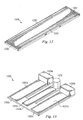
Referring to Fig. 7, illustrated is a perspective view of an embodiment of an apparatus
700 according to aspects of the present disclosure is illustrated. The apparatus 700 achieves
two independent planes or directions of movement, and includes a base 710 attached to a
piezoelectric element 750.
-
The base 710 may be substantially similar in composition and manufacture to the base
110 shown in Fig. 1a. In one embodiment, the length and width of the base 110 may both
range from about 5 millimeters to about 20 millimeters. In other embodiments, the base 110
may have a length and width both ranging between about 50 microns and about 200 microns.
-
The piezoelectric element 750 is generally shaped as an angled member, possibly
including two or more segments coupled or integrally formed together. The angle of the
piezoelectric element 750 may range between about 45 degrees and about 135 degrees. The
piezoelectric element 750 may comprise similar materials as the piezoelectric elements
described above, and may be manufactured according to similar principles. In one
embodiment, the piezoelectric element 750 may range from about 0.5 centimeters to about 15
centimeters in length and width. In other embodiments, the piezoelectric element 750 may
range between about 50 microns and about 200 microns in length and width.
-
The apparatus 700 may also include a friction element 770 attached near a vertex or
junction of two or more segments of the piezoelectric element 750. The friction element 770
may be substantially similar in composition and manufacture to the friction element 170
shown in Fig. 1a.
-
The apparatus 700 also includes two driven elements 790a, 790b. The driven element
790a is configured to slide relative to the base 710 in a first direction 705, and the driven
element 790b is configured to slide relative to the driven element 790a (and, hence, the base
710) in a second direction 707. In one embodiment, the first and second directions 705, 707
are substantially orthogonal, although other relative orientations of the first and second
directions 705, 707 are within the scope of the present disclosure.
-
The piezoelectric element 750 may attach to the base 710 at two ends each distal from
the attachment point of the friction element 770. In this manner, an electrical signal may be
applied to the piezoelectric element 750 to produce actuation of the piezoelectric element 750
along at least two planes or directions of movement. The two directions of movement may
correspond to movement of the two separate pieces of the driven element 790a, 790b, which
are configured to manipulate the surface of the driven element 790b in two dimensions, as
described above. The driven element components 790a-b may each be substantially similar
in composition and manufacture as the driven element 190 shown in Fig. 1a. Coarse
positioning may be achieved, for example, by application of a fluctuating electrical signal to
produce slip-stick movement of one or both of the driven elements 790a, 790b. Fine
positioning may be achieved, for example, by application of a non-fluctuating electrical
signal to the piezoelectric element 750.
-
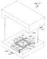
Referring to Fig. 8, a cutaway view of an embodiment of an apparatus 800 according
to aspects of the present disclosure is illustrated. The apparatus 800 may be configured to
produce rotary motion in a driven element 890. The apparatus 800 includes a base 810 and
an insulator 830, wherein the insulator 830 attaches a piezoelectric element 850 to the base
810. The composition and manufacture of the base 810, insulator 830, and piezoelectric
element 850 may be similar to those in embodiments previously described. The piezoelectric
element 850 may have an attached friction element 870, which slidably frictionally engages
the driven element 890. The driven element 890 may be substantially similar in composition
and manufacture to the driven element 190 shown in Fig. 1a, and may be substantially disc-shaped,
possibly having a diameter ranging between about 0.5 cm and about 15 cm. In other
embodiments, the driven element 890 may have a diameter ranging from about 50 microns to
about 200 microns.
-
The driven element 890 may be rotatably attached to the base 810. Rotation of the
driven element 890 may be achieved by applying a first fluctuating electrical signal to the
piezoelectric element 850. A fluctuating electrical signal may generate a slip-stick movement
of the driven element 890. Slip-stick movement may be employed to achieve coarse
positioning, while fine positioning may be achieved by application of a non-fluctuating
electrical signal. Rotation of the driven element 890 in an opposite direction may be
achieved by application of a fluctuating electrical signal of a different form than the first.
-
Referring to Fig. 9, a perspective view of an embodiment of an apparatus 900
according to aspects of the present disclosure is illustrated. The apparatus 900 may produce
rotational movement in driven elements 990a-b and is similar to previously described
apparatus 800. The apparatus 900 comprises a base 910 and a bracket 912 for attachment of
piezoelectric elements 950a, 950b. The bracket 912 may comprise aluminum oxide, ceramic,
beryllium, brass, gold, and/or other materials. Electrodes 955a, 955b are employed in the
illustrated embodiment to apply electrical signals to piezoelectric elements 950a and 950b,
respectively. In this configuration, the piezoelectric elements 950a, 950b may have attached
friction elements 970a, 970b, respectively. The friction elements 970a, 970b may
independently engage driven element 990a, driven element 990b, or both (e.g., friction
elements 970a and/or 970b may be positioned on each of opposing surfaces of elements 950a
and/or 950b). In the embodiment of Fig. 9, the apparatus 900 includes two piezoelectric
elements 950a, 950b and two driven elements 990a, 990b, but the apparatus 900 may include
any number of driven elements engaged by any number of piezoelectric elements within the
scope of the present disclosure.
-
The driven elements 990a, 990b may be rotationally and coaxially attached along a
central axis. The driven elements 990a, 990b may be configured to rotate only as a fixed
unit, or may be configured to rotate independently. Coarse rotational motion of the driven
elements 990a, 990b may be controlled by slip-stick motion resulting from fluctuating
electrical signals, which may be applied to the piezoelectric elements 950a, 950b, via
electrodes 955a, 955b. The signal may be applied such that one piezoelectric element (for
example, element 950a) is in a "slip" phase, while the other piezoelectric element (for
example, element 950b) is in a "stick" phase. Non-fluctuating electrical signals may also be
applied to either, or both, of the piezoelectric elements 950a, 950b to control fine positioning.
-
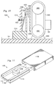
Referring to Fig. 10, a side view of another embodiment of a microelectronic
apparatus 1000 according to aspects of the present disclosure is illustrated. The apparatus
1000 may produce substantially orthogonal motion of driven elements 1090, 1091 each
relative to a substrate 1011. The apparatus 1000 comprises a base 1010 mounted on or over
the substrate 1011. The materials and method of manufacture for the base 1010 and substrate
1011 may be substantially similar to those described regarding the bases of previously
described embodiments. The base 1010 and substrate 1011 may be separate components
attached by adhesive and/or other means, or they may be integral to one another.
-
A biasing element 1015, which may correspond in materials and manufacture to
biasing elements heretofore described, possibly with an attached spacer 1020, also
corresponding in materials and manufacture to spacers heretofore described, is mounted to
the base 1010. The tension of the biasing element 1015 may be adjustable, such as via a
threaded fastener 1025 and/or other means. The biasing element 1015 biases the
piezoelectric element 1050 and/or an attached friction element 1070 against a wear plate
1095, which is attached to driven element 1090. The friction element 1070 and wear plate
1095 may be substantially similar in composition and manufacture to friction elements and
wear plates previously described, respectively. In some embodiments, the wear plate 1095
may be optional.
-
A piezoelectric element 1050 operates to move the driven element 1090 for coarse
positioning via slip-stick motion resulting from the application of a fluctuating electrical
signal. To achieve fine positioning, a non-fluctuating electrical signal may be applied to the
piezoelectric element 1050. The piezoelectric element 1050 may be similar in composition
and manufacture and piezoelectric elements heretofore described. In the illustrated
embodiment, the driven element 1090 is attached to the driven element 1091 via a looped
band 1092. The driven elements 1090, 1091 may be substantially similar in composition and
manufacture to driven elements previously described. However, the second driven element
1091 may be similar to, or different from, the first driven element 1090.
-
The band 1092 connecting the driven elements 1090, 1091 may be silicon, rubber,
stainless steel, and/or other materials. The length of the band 1092 may range between about
1.5 centimeters and about 45 centimeters, and the band 1092 may have a thickness ranging
between about 100 microns and about 250 microns. The band 1092 may be supported by
rollers or tensioners 1093, 1094, which may be substantially cylindrical. The tensioners
1093, 1094 may comprise silicon, metal, and/or other materials. The dimensions of the
tensioners may be set according to the dimension of the band 1092 and piezoelectric element
1050. The tensioners 1093, 1094 may be rotatably attached to the substrate 1011 by support
structure 1099, which may include bearings, posts, etc. The band 1092 may translate
movement of the first driven element 1090 to the second driven element 1091. The
dimensions given above reference a macro-scale embodiment, but it may be possible to scale
the apparatus 1000 to smaller sizes, possibly including a micro-scale embodiment.
-
Referring to Fig. 11, a perspective view of an embodiment of an apparatus 1100
according to aspects of the present disclosure is illustrated. The apparatus 1100 may be
substantially similar in materials, construction, and dimension as apparatus 100 (Fig. 1a). For
example, base 1110 and driven element 1190 may be similar in materials, construction, and
dimension to base 110 and driven element 190 of apparatus 100, respectively. The apparatus
1100 features a piezoelectric element 1150 that may be anchored at both ends to the base
1110. The element 1150 may also be sectioned or partitioned, including two or more
portions 1151, 1152, which may be electrically isolated from one another. Insulators 1130a,
1130b may serve to anchor the piezoelectric element 1150 to the base 1110. The insulators
1130a, 1130b may be substantially similar to insulator 130 of apparatus 100. The
piezoelectric element 1150 may be substantially reed-shaped and may otherwise be similar to
piezoelectric element 150 of apparatus 100. A friction element 1170 may be attached at a
substantially central point on the piezoelectric element 1150. The friction element 1170 may
be substantially similar to friction element 170 of apparatus 100. In operation, the apparatus
1100 may operate by application of actuating signals of differing polarities to different
sections 1151, 1152 of the piezoelectric element 1150. In such case, a slip-stick movement of
the friction element against the slide table 1190 may result from a contraction in one section
(e.g., section 1151) of the piezoelectric element 1150 with a corresponding elongation in
another section (e.g., section 1152).
-
Referring to Fig. 12, a perspective view an embodiment of an electrode configuration
1200 for a piezoelectric element 1250 according to aspects of the present disclosure is
illustrated. Piezoelectric element 1250 may be substantially similar to piezoelectric elements
previously discussed, such as piezoelectric element 150 (Fig. 1a). A main electrode 1231
may be placed on substantially the full length of piezoelectric element 1250. In some
embodiments, the main electrode 1231 may be a plurality of electrodes. The placement of
the main electrode 1231 may also vary from that shown. The main electrode 1231 may
comprise copper, gold, and/or other materials which may be deposited onto piezoelectric
element 1250 or formed integrally therewith. Correction electrodes 1232, 1233 may be
placed on substantially the full length of the piezoelectric element 1250, possibly on either
side of the main electrode 1231. The correction electrodes 1232, 1233 may vary in number
and placement from that shown. The correction electrodes 1232, 1233 may comprise copper,
gold, and/or other materials, which may be deposited onto piezoelectric element 1250, or
formed integrally therewith.
-
A friction element (not shown) such as friction element 170 (Fig. 1a) may be attached
to the piezoelectric element 1250 to transfer movement to a driven element (not shown). In
operation, the main electrode 1231 may be used to provide an actuating signal to the
piezoelectric element 1250. The actuating signal may be as previously described with respect
to previous embodiments (e.g., a waveform or a non-fluctuating voltage). The correction
electrodes 1232, 1233 may be used instead of, or in addition to, the main electrode 1231 to
provide corrections in the deflection or movement of the piezoelectric element 1250. Similar
to the main electrode 1231, the correction electrodes 1231, 1232 may be provided with
waveform voltage or a non-fluctuating voltage, which may be smaller, larger, or the same as
the voltage provided to the main electrode 1231.
-
Referring to Fig. 13, a perspective view of another embodiment of a piezoelectric
element 1300 according to aspects of the present disclosure is illustrated. The piezoelectric
element 1300 may be utilized in one or more of the apparatus previously discussed (e.g.,
apparatus 100) or some other device. The apparatus 1300 may be mounted to a base (e.g.
base 110 of Fig. 1a) by mounts 1330a, 1330b, for example. In some embodiments, the
placement of the mounts will vary from the placement shown. The piezoelectric element
1300 may be similar in materials and construction as previously described piezoelectric
elements. The piezoelectric element 1300 may have one or more piezoelectric members
1350a-c. The members 1350a-c may be formed integrally or formed separately and
subsequently attached together. Electrodes 1331a, 1331b, 1331c may be attached along
substantially the length of the members 1350a, 1350b, 1350c, respectively. The electrodes
1331a, 1331b, 1331c may be substantially similar to electrode 1231 (Fig. 12).
-
In operation, the electrodes 1331a-c may be used to apply an actuating signal to the
respective members 1350a-c. As previously described the actuating signal may be a
waveform or a non-fluctuating voltage. The polarity of the signal applied to members 1350b
via electrode 1331b may be opposite to the polarity of the signal applied to members 1350a,
1350c via electrodes 1331a, 1331c, respectively. Thus, an elongation of member 1350b may
correspond to a contraction of members 1350a, 1350c, and vice-versa. A friction element
1370 may be attached to the piezoelectric element 1300 to interface with a driven element
(not shown) such as slide bed 190 (Fig. 1a). The friction element 1370 may be similar in
materials and construction to friction elements previously described (e.g. friction element 170
of Fig. 1a). Thermal expansion in the piezoelectric element 1300, which could lead to an
unwanted displacement of the friction element 1370, may be alleviated by expansion in an
opposite direction of member 1350b relative to members 1350a, 1350c.
-
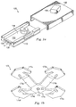
Referring to Fig. 14, a perspective view of anther embodiment of an apparatus 1400
of the present disclosure is illustrated. The apparatus 1400 may be similar in materials,
construction, and dimension to apparatus 700 (Fig. 7). Like apparatus 700, the apparatus
1400 may achieve two independent planes of movement (e.g., 1405, 1407). The apparatus
1400 may have multiple piezoelectric elements 1450a-h. In some embodiments, two or more
of the piezoelectric elements 1450a-h may be combined or manufactured as a single angled
piezoelectric element such as piezoelectric element 750 (Fig. 7). The apparatus 1400 may
have a plurality of friction elements 1470, 1471, 1472, 1473. The friction elements 1470,
1471, 1472, 1473 may be substantially similar to friction element 770 (Fig. 7). The
piezoelectric elements 1450a-h may elongate or contract as in response to a waveform
previously described in order to achieve slip stick motion for coarse positioning. Fine
positioning may be achieved by application of a non-fluctuating voltage, as previously
described, to one or more of the piezoelectric elements 1450a-h.
-
The present disclosure provides an apparatus including, in one embodiment, a base
configured to slidably engage a driven element. A piezoelectric element interposes the base
and the driven element and is attached to the base proximate a first piezoelectric element end.
A friction element is attached proximate a second piezoelectric element end and is configured
to selectively engage the driven element.
-
The present disclosure also introduces an apparatus including, in one embodiment, a
slide bed having a recess therein, a slide table having a wear plate on an inner surface, and a
piezoelectric reed with attached friction element. The reed is mounted in the slide bed recess
and frictionally engages the wear plate via the friction element.
-
Another embodiment of an apparatus constructed according to aspects of the present
disclosure includes a base configured to slidably engage a driven element, and first and
second piezoelectric elements, each parallel to the base. A friction element is proximate a
junction of the first and second piezoelectric elements and extends in first and second
directions.
-
Another embodiment of an apparatus according to aspects of the present disclosure
includes a rotatable element rotatably coupled to a substrate. In such an embodiment, a
piezoelectric element is coupled to the substrate and a friction element is coupled to the
piezoelectric element. The friction element is configured to frictionally engage the rotatable
element to impart rotary motion thereto.
-
An apparatus constructed according to aspects of the present disclosure may also
include first and second driven elements and a piezoelectric element, which slidably engages
the first driven element. The first and second driven elements may each be coupled to one
another via a continuous flexible band supported by at least one roller.
-
Although embodiments of the present disclosure have been described in detail,
those skilled in the art should understand that they can make various changes, substitutions
and alterations herein.