EP1576649B1 - Stackable layers containing encapsulated integrated circuit chips with one or more overlying interconnect layers and a method of making the same - Google Patents
Stackable layers containing encapsulated integrated circuit chips with one or more overlying interconnect layers and a method of making the same Download PDFInfo
- Publication number
- EP1576649B1 EP1576649B1 EP02789292A EP02789292A EP1576649B1 EP 1576649 B1 EP1576649 B1 EP 1576649B1 EP 02789292 A EP02789292 A EP 02789292A EP 02789292 A EP02789292 A EP 02789292A EP 1576649 B1 EP1576649 B1 EP 1576649B1
- Authority
- EP
- European Patent Office
- Prior art keywords
- integrated circuit
- circuit chip
- interconnect assembly
- interconnect
- test pad
- Prior art date
- Legal status (The legal status is an assumption and is not a legal conclusion. Google has not performed a legal analysis and makes no representation as to the accuracy of the status listed.)
- Expired - Lifetime
Links
Images


Classifications
-
- H—ELECTRICITY
- H01—ELECTRIC ELEMENTS
- H01L—SEMICONDUCTOR DEVICES NOT COVERED BY CLASS H10
- H01L21/00—Processes or apparatus adapted for the manufacture or treatment of semiconductor or solid state devices or of parts thereof
- H01L21/02—Manufacture or treatment of semiconductor devices or of parts thereof
- H01L21/04—Manufacture or treatment of semiconductor devices or of parts thereof the devices having at least one potential-jump barrier or surface barrier, e.g. PN junction, depletion layer or carrier concentration layer
- H01L21/50—Assembly of semiconductor devices using processes or apparatus not provided for in a single one of the subgroups H01L21/06 - H01L21/326, e.g. sealing of a cap to a base of a container
- H01L21/56—Encapsulations, e.g. encapsulation layers, coatings
- H01L21/568—Temporary substrate used as encapsulation process aid
-
- H—ELECTRICITY
- H01—ELECTRIC ELEMENTS
- H01L—SEMICONDUCTOR DEVICES NOT COVERED BY CLASS H10
- H01L21/00—Processes or apparatus adapted for the manufacture or treatment of semiconductor or solid state devices or of parts thereof
- H01L21/67—Apparatus specially adapted for handling semiconductor or electric solid state devices during manufacture or treatment thereof; Apparatus specially adapted for handling wafers during manufacture or treatment of semiconductor or electric solid state devices or components ; Apparatus not specifically provided for elsewhere
- H01L21/683—Apparatus specially adapted for handling semiconductor or electric solid state devices during manufacture or treatment thereof; Apparatus specially adapted for handling wafers during manufacture or treatment of semiconductor or electric solid state devices or components ; Apparatus not specifically provided for elsewhere for supporting or gripping
- H01L21/6835—Apparatus specially adapted for handling semiconductor or electric solid state devices during manufacture or treatment thereof; Apparatus specially adapted for handling wafers during manufacture or treatment of semiconductor or electric solid state devices or components ; Apparatus not specifically provided for elsewhere for supporting or gripping using temporarily an auxiliary support
-
- H—ELECTRICITY
- H01—ELECTRIC ELEMENTS
- H01L—SEMICONDUCTOR DEVICES NOT COVERED BY CLASS H10
- H01L22/00—Testing or measuring during manufacture or treatment; Reliability measurements, i.e. testing of parts without further processing to modify the parts as such; Structural arrangements therefor
- H01L22/30—Structural arrangements specially adapted for testing or measuring during manufacture or treatment, or specially adapted for reliability measurements
- H01L22/32—Additional lead-in metallisation on a device or substrate, e.g. additional pads or pad portions, lines in the scribe line, sacrificed conductors
-
- H—ELECTRICITY
- H01—ELECTRIC ELEMENTS
- H01L—SEMICONDUCTOR DEVICES NOT COVERED BY CLASS H10
- H01L23/00—Details of semiconductor or other solid state devices
- H01L23/28—Encapsulations, e.g. encapsulating layers, coatings, e.g. for protection
- H01L23/31—Encapsulations, e.g. encapsulating layers, coatings, e.g. for protection characterised by the arrangement or shape
- H01L23/3107—Encapsulations, e.g. encapsulating layers, coatings, e.g. for protection characterised by the arrangement or shape the device being completely enclosed
- H01L23/3121—Encapsulations, e.g. encapsulating layers, coatings, e.g. for protection characterised by the arrangement or shape the device being completely enclosed a substrate forming part of the encapsulation
-
- H—ELECTRICITY
- H01—ELECTRIC ELEMENTS
- H01L—SEMICONDUCTOR DEVICES NOT COVERED BY CLASS H10
- H01L23/00—Details of semiconductor or other solid state devices
- H01L23/52—Arrangements for conducting electric current within the device in operation from one component to another, i.e. interconnections, e.g. wires, lead frames
- H01L23/538—Arrangements for conducting electric current within the device in operation from one component to another, i.e. interconnections, e.g. wires, lead frames the interconnection structure between a plurality of semiconductor chips being formed on, or in, insulating substrates
- H01L23/5388—Arrangements for conducting electric current within the device in operation from one component to another, i.e. interconnections, e.g. wires, lead frames the interconnection structure between a plurality of semiconductor chips being formed on, or in, insulating substrates for flat cards, e.g. credit cards
-
- H—ELECTRICITY
- H01—ELECTRIC ELEMENTS
- H01L—SEMICONDUCTOR DEVICES NOT COVERED BY CLASS H10
- H01L25/00—Assemblies consisting of a plurality of individual semiconductor or other solid state devices ; Multistep manufacturing processes thereof
- H01L25/03—Assemblies consisting of a plurality of individual semiconductor or other solid state devices ; Multistep manufacturing processes thereof all the devices being of a type provided for in the same subgroup of groups H01L27/00 - H01L33/00, or in a single subclass of H10K, H10N, e.g. assemblies of rectifier diodes
- H01L25/10—Assemblies consisting of a plurality of individual semiconductor or other solid state devices ; Multistep manufacturing processes thereof all the devices being of a type provided for in the same subgroup of groups H01L27/00 - H01L33/00, or in a single subclass of H10K, H10N, e.g. assemblies of rectifier diodes the devices having separate containers
- H01L25/105—Assemblies consisting of a plurality of individual semiconductor or other solid state devices ; Multistep manufacturing processes thereof all the devices being of a type provided for in the same subgroup of groups H01L27/00 - H01L33/00, or in a single subclass of H10K, H10N, e.g. assemblies of rectifier diodes the devices having separate containers the devices being of a type provided for in group H01L27/00
-
- H—ELECTRICITY
- H01—ELECTRIC ELEMENTS
- H01L—SEMICONDUCTOR DEVICES NOT COVERED BY CLASS H10
- H01L2221/00—Processes or apparatus adapted for the manufacture or treatment of semiconductor or solid state devices or of parts thereof covered by H01L21/00
- H01L2221/67—Apparatus for handling semiconductor or electric solid state devices during manufacture or treatment thereof; Apparatus for handling wafers during manufacture or treatment of semiconductor or electric solid state devices or components; Apparatus not specifically provided for elsewhere
- H01L2221/683—Apparatus for handling semiconductor or electric solid state devices during manufacture or treatment thereof; Apparatus for handling wafers during manufacture or treatment of semiconductor or electric solid state devices or components; Apparatus not specifically provided for elsewhere for supporting or gripping
- H01L2221/68304—Apparatus for handling semiconductor or electric solid state devices during manufacture or treatment thereof; Apparatus for handling wafers during manufacture or treatment of semiconductor or electric solid state devices or components; Apparatus not specifically provided for elsewhere for supporting or gripping using temporarily an auxiliary support
- H01L2221/68359—Apparatus for handling semiconductor or electric solid state devices during manufacture or treatment thereof; Apparatus for handling wafers during manufacture or treatment of semiconductor or electric solid state devices or components; Apparatus not specifically provided for elsewhere for supporting or gripping using temporarily an auxiliary support used as a support during manufacture of interconnect decals or build up layers
-
- H—ELECTRICITY
- H01—ELECTRIC ELEMENTS
- H01L—SEMICONDUCTOR DEVICES NOT COVERED BY CLASS H10
- H01L2224/00—Indexing scheme for arrangements for connecting or disconnecting semiconductor or solid-state bodies and methods related thereto as covered by H01L24/00
- H01L2224/01—Means for bonding being attached to, or being formed on, the surface to be connected, e.g. chip-to-package, die-attach, "first-level" interconnects; Manufacturing methods related thereto
- H01L2224/10—Bump connectors; Manufacturing methods related thereto
- H01L2224/15—Structure, shape, material or disposition of the bump connectors after the connecting process
- H01L2224/16—Structure, shape, material or disposition of the bump connectors after the connecting process of an individual bump connector
- H01L2224/161—Disposition
- H01L2224/16151—Disposition the bump connector connecting between a semiconductor or solid-state body and an item not being a semiconductor or solid-state body, e.g. chip-to-substrate, chip-to-passive
- H01L2224/16221—Disposition the bump connector connecting between a semiconductor or solid-state body and an item not being a semiconductor or solid-state body, e.g. chip-to-substrate, chip-to-passive the body and the item being stacked
- H01L2224/16225—Disposition the bump connector connecting between a semiconductor or solid-state body and an item not being a semiconductor or solid-state body, e.g. chip-to-substrate, chip-to-passive the body and the item being stacked the item being non-metallic, e.g. insulating substrate with or without metallisation
- H01L2224/16227—Disposition the bump connector connecting between a semiconductor or solid-state body and an item not being a semiconductor or solid-state body, e.g. chip-to-substrate, chip-to-passive the body and the item being stacked the item being non-metallic, e.g. insulating substrate with or without metallisation the bump connector connecting to a bond pad of the item
-
- H—ELECTRICITY
- H01—ELECTRIC ELEMENTS
- H01L—SEMICONDUCTOR DEVICES NOT COVERED BY CLASS H10
- H01L2224/00—Indexing scheme for arrangements for connecting or disconnecting semiconductor or solid-state bodies and methods related thereto as covered by H01L24/00
- H01L2224/73—Means for bonding being of different types provided for in two or more of groups H01L2224/10, H01L2224/18, H01L2224/26, H01L2224/34, H01L2224/42, H01L2224/50, H01L2224/63, H01L2224/71
- H01L2224/732—Location after the connecting process
- H01L2224/73201—Location after the connecting process on the same surface
- H01L2224/73203—Bump and layer connectors
- H01L2224/73204—Bump and layer connectors the bump connector being embedded into the layer connector
-
- H—ELECTRICITY
- H01—ELECTRIC ELEMENTS
- H01L—SEMICONDUCTOR DEVICES NOT COVERED BY CLASS H10
- H01L2225/00—Details relating to assemblies covered by the group H01L25/00 but not provided for in its subgroups
- H01L2225/03—All the devices being of a type provided for in the same subgroup of groups H01L27/00 - H01L33/648 and H10K99/00
- H01L2225/10—All the devices being of a type provided for in the same subgroup of groups H01L27/00 - H01L33/648 and H10K99/00 the devices having separate containers
- H01L2225/1005—All the devices being of a type provided for in the same subgroup of groups H01L27/00 - H01L33/648 and H10K99/00 the devices having separate containers the devices being of a type provided for in group H01L27/00
- H01L2225/1011—All the devices being of a type provided for in the same subgroup of groups H01L27/00 - H01L33/648 and H10K99/00 the devices having separate containers the devices being of a type provided for in group H01L27/00 the containers being in a stacked arrangement
- H01L2225/1017—All the devices being of a type provided for in the same subgroup of groups H01L27/00 - H01L33/648 and H10K99/00 the devices having separate containers the devices being of a type provided for in group H01L27/00 the containers being in a stacked arrangement the lowermost container comprising a device support
- H01L2225/1023—All the devices being of a type provided for in the same subgroup of groups H01L27/00 - H01L33/648 and H10K99/00 the devices having separate containers the devices being of a type provided for in group H01L27/00 the containers being in a stacked arrangement the lowermost container comprising a device support the support being an insulating substrate
-
- H—ELECTRICITY
- H01—ELECTRIC ELEMENTS
- H01L—SEMICONDUCTOR DEVICES NOT COVERED BY CLASS H10
- H01L2225/00—Details relating to assemblies covered by the group H01L25/00 but not provided for in its subgroups
- H01L2225/03—All the devices being of a type provided for in the same subgroup of groups H01L27/00 - H01L33/648 and H10K99/00
- H01L2225/10—All the devices being of a type provided for in the same subgroup of groups H01L27/00 - H01L33/648 and H10K99/00 the devices having separate containers
- H01L2225/1005—All the devices being of a type provided for in the same subgroup of groups H01L27/00 - H01L33/648 and H10K99/00 the devices having separate containers the devices being of a type provided for in group H01L27/00
- H01L2225/1011—All the devices being of a type provided for in the same subgroup of groups H01L27/00 - H01L33/648 and H10K99/00 the devices having separate containers the devices being of a type provided for in group H01L27/00 the containers being in a stacked arrangement
- H01L2225/1047—Details of electrical connections between containers
- H01L2225/1064—Electrical connections provided on a side surface of one or more of the containers
-
- H—ELECTRICITY
- H01—ELECTRIC ELEMENTS
- H01L—SEMICONDUCTOR DEVICES NOT COVERED BY CLASS H10
- H01L2924/00—Indexing scheme for arrangements or methods for connecting or disconnecting semiconductor or solid-state bodies as covered by H01L24/00
- H01L2924/10—Details of semiconductor or other solid state devices to be connected
- H01L2924/11—Device type
- H01L2924/14—Integrated circuits
- H01L2924/143—Digital devices
- H01L2924/1433—Application-specific integrated circuit [ASIC]
-
- H—ELECTRICITY
- H01—ELECTRIC ELEMENTS
- H01L—SEMICONDUCTOR DEVICES NOT COVERED BY CLASS H10
- H01L2924/00—Indexing scheme for arrangements or methods for connecting or disconnecting semiconductor or solid-state bodies as covered by H01L24/00
- H01L2924/15—Details of package parts other than the semiconductor or other solid state devices to be connected
- H01L2924/181—Encapsulation
- H01L2924/1815—Shape
- H01L2924/1816—Exposing the passive side of the semiconductor or solid-state body
- H01L2924/18161—Exposing the passive side of the semiconductor or solid-state body of a flip chip
Definitions
- This invention relates to the dense packaging of electronic circuitry, and specifically to the stacking of integrated circuit (IC) chips, or die.
- IC integrated circuit
- Stackable IC chip layers were disclosed in U.S. Pat. No. 5,953,588 which permit chips having different functions and therefore different areas to be stacked as if they were same size chips, using stacking and electrical connection techniques and tools which have been developed for same size chips.
- the new units were referred to as "neo” (or “pseudo” or “virtual") chips.
- that technology permits the processing and stacking of chips purchased as individual die, which are more readily available than chips purchased in wafer form.
- the chips purchased as individual die are generally "known good” die, which have been "burned in”, and are therefore pre-tested prior to stacking.
- a re-wafering process in which a neo-wafer is formed encapsulating known good chips, so that the chips can be prepared for stacking by covering their active surfaces with a dielectric layer, forming vias through the dielectric layer to reach the terminals on the respective chips, and metallizing to provide electrical connections from the chip terminals to side surfaces of the layer, which are created when the neo-wafer is diced, or sliced, to provide individual layers ready for stacking.
- the manufacturing process is much more cost effective if the neo-wafer contains a plurality of pre-formed, pre-tested chips which can be simultaneously prepared for stacking.
- the neo-wafer is subsequently diced to form individual layers ready for stacking. In effect, two wafering and dicing processes are used to facilitate stacking of chip-encapsulating layers.
- the primary challenge in using a neo-wafer containing multiple die is the accurate location of each die. With multiple die in the wafer, the accuracy necessary to locate each die prior to potting creates a potential alignment problem.
- the re-wafering process was improved in U.S. Patent 6,117,704 by making location of chips (die) in the neo-wafer highly accurate, and by making it more feasible to include multiple chips in the neo-wafer.
- the neo-wafer is so structured that each chip it contains is precisely located by use of a single masking step to obtain exact location of the known good chips, which are inserted in the neo-wafer and then covered by potting material. Then the chips in the neo-wafer are simultaneously processed to prepare them for stacking. They are stacked after they have been diced from the neo-wafer.
- the locations of the chips in the neo-wafer are controlled by photo patterning (photo-lithography), their relative locations are determined with the very high precision inherent in the use of a single mask to control the locations of all chips in the neo-wafer.
- Another advantage of the improved process is that any leakage of potting material onto the active (upper) surfaces of the chips in the neo-wafer does not affect the electrical terminals on the chips, so that removal of any such leaked material is not required, and increased reliability of the electrical connection is obtained.
- the benefits of the improved prior art are obtained by using a wafer frame, sometimes called a "picture frame", having a plurality of separate chambers, or cavities, into which the individual known good chips are inserted.
- the chips have conductive bumps which extend into and through pre-formed small holes (vias) in the surface of the wafer frame.
- the via holes have been formed using photo-lithography with a single mask for the entire neo-wafer, thus insuring precise location of the via holes relative to one another. This insures precise location of the separate chips relative to one another, and provides terminals accessible for electrical connections.
- US-B1-6 235 552 discloses a method for manufacturing a chip scale package including providing a redistribution substrate, attaching a semiconductor wafer to the redistribution substrate, forming external terminals on the redistribution substrate, and separating the semiconductor wafer and the redistribution substrate into individual integrated circuits.
- the invention is a method of preparing a pre-formed integrated circuit chip for encapsulation in an electronic package according to claim 1.
- a pre-formed integrated circuit chip is encapsulated into an electronic package, by forming an interconnect assembly separately from the pre-formed integrated circuit chip. If the interconnect assembly tests good it is bonded to the prepared integrated circuit chip.
- the interconnect assembly is flip bonded to the prepared integrated circuit chip.
- the bonded interconnect assembly and the prepared integrated circuit chip are passivated or potted into an integral structure to provide the electronic package.
- At least one test pad is defined in an interconnect layer, which test pad can be accessed and electrically connected on opposing sides of the test pad.
- the prepared integrated circuit chip is underfilled with an insulating material to remove all voids between the prepared integrated circuit chip and the interconnect assembly.
- the prepared integrated circuit chip is then thinned.
- the test pad is accessed to test the prepared integrated circuit chip.
- a plurality of interconnect assembly and prepared integrated circuit chips are bonded together to form a corresponding plurality of electronic packages.
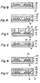
- Figs. 1a - 1n are diagrammatic side cross-sectional views of what is called here a "reverse neo process”.
- Fig. 1a begins with the preparation of aluminum shim stock 10. In the illustrated embodiment of aluminum shim stock is approximate 30 mills in thickness.
- a polyimide layer 12 is then disposed on aluminum layer 10. The polyimide layer is cured.
- a field metal layer 14 is applied on top of cured polyimide layer 12. Photoresist 16 is then disposed on metal layer 14 as shown in the side diagrammatic view of Fig. 1d and lithographically patterned according to conventional techniques.
- Gold or other conductive metal 18 is then disposed into openings and 20 defined in photoresist layers 16 as shown in Fig. 1e .
- the photoresist layer is then removed and field metal 14 etched leaving the structure depicted in Fig. 1f in which gold pads 18 are supported on field metal 14 on top of a polyimide coated aluminum shim 10.
- a polyimide layer 22 is then disposed on gold pads 18 of Fig. 1f .
- a photoresist layer 24 is then disposed upon polyimide layer 22 as depicted in Fig. 1h .
- Photo resist layer 25 is imaged and developed along with polyimide layer 20 to thereby define openings 26 through polyimide layer 24 and photoresist layer 22 to expose a selected portion of gold pad 18 as shown Fig. 1i .
- photoresist layer 24 is removed and polyimide layer 22 is cured leaving the structure shown in Fig. 1j in which openings 26 remain defined above gold pads 18.
- a field in the layer metal 26 is then disposed on polyimide layer 22 into openings 26 which have been previously defined above gold pads 18 to create a field metal layer 28 in which pockets or wells 30 are defined.
- a photoresist layer 32 is then disposed on top of field layer 28 as shown in Fig. 1l .
- Photoresist layer 32 is imaged and developed to define openings 34 into which a gold layer 36 is electroplated as shown in Fig. 1m .
- Photoresist layer 32 is then stripped away and field layer 28 is etched to leave the resulting structure as shown in Fig. 1n in which there are gold contact pads 36 positioned on top polyimide layer 22, which gold contact pads 36 in turn are connected to gold pads18 which are lying there below.
- Figs. 1a - 1n depict the process by which a metallization layer is constructed. If additional metallization layers are desired, the steps of Figs. 1g - 1n can be repeated as many times as necessary to created additional stacked layers of interconnects. In practice 3 or 4 layers are usually the most number ever needed.
- Figs. 2a - 2c represent the solder bumping of the die.
- a die 40 is obtained from a semiconductor wafer. It is to be understood the die 40 has been previously processed and may have any type of device or semiconductor devices already defined within it.
- Fig. 2b a plurality of metallic bumps are then applied in a predefined pattern on upper surface 44 of die 40 to provide contact to connection points on die 40.
- the solder layers 46 are then disposed on each of bumps 42 to result in the structure shown in Fig. 2c .
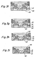
- Fig. 3a illustrates the flip chip bonding steps of the invention.
- the intermediate structure as shown in the completed step in Fig. 1n , is combined with the intermediate structure shown in the completed step of Fig. 2c .
- the structure of Fig.1n is for the purposes of Fig. 3a denoted collectively by reference numeral 48.
- the completed structure Fig. 2c is shown in Fig. 3a collectively denoted by the reference numeral 50.
- Die structure 50 is thus flipped and placed on top of interconnect structure 48 as depicted in Fig. 3a .
- the solder bumps 46 had been devised so they are aligned with gold contact pads 36.
- the flip structures are then bonded together to make secure mechanical and electrical connection at their points of contact.
- Fig. 3b The open space 52 between die structure 50 and interconnect structure 48 shown in Fig. 3a is filled with an insulating material 54 such as an epoxy under fill. Thereafter the entire bonded and completed structure as shown in Fig. 3b is potted with conventional potting material to form a monolithic passivated package as shown in Fig. 3c .
- Potted die structure 50 is thinned by grinding or other means to the desired final thickness forming a thin semiconductor wafer 56 as shown in Fig. 3d .
- Active semiconductor devices remain unaffected in the nonthinned or remaining portion of wafer 56.
- Aluminum layer 10, which has served the purpose of a structural substrate during the construction steps is then released by conventional means in step 3e and removed leaving polyimide layer 12 as the lowermost layer of the device as depicted in Fig. 3e .
- a masking layer 58 of photoresist is then disposed on polyimide layer 12 as shown in Fig. 3f and is photolithographically imaged to define openings 60 which will serve to provide the structure for the test pads 14, 18.
- the exposed polyimide layer 12 in openings 60 is then etched away to expose field layer metal 14 of gold pads 18.
- Etched mask 58 is then removed as shown in Fig. 3h . This then allows the semiconductor devices in thinned wafer 56 to be accessed and tested through test pads 14, 18 through openings 62 in polyimide layer 12.
- Fig. 4a is a diagrammatic side cross-sectional view of a further embodiment of the reverse neo process for high-volume fabrication.
- a first set of wafers generally to know by reference numeral 70, is processed along with a second wafer 72.
- An interconnect layer 74 such as described in connection Figs. 1a-1n is prepared and prepackaged chip devices 76 are then flip bonded to interconnect layer 74.
- the first wafer 70 includes a flash and SRAM memory chip and the second wafer includes an ASIC chip. It is of course to be understood that any number and kind of the packaged integrated circuit chips may be employed.
- the epoxies are cured, the devices underfilled and the transfer devices are molded to form the electronics packaged using potting 78 in the manner as described above.
- Fig. 4b the two wafers of Fig. 4a are combined. Any carriers which may be present on either wafer is released from the wafer substrate and the two wafers are attached or epoxied together as shown in Fig. 4b .
- wafers 70 and 72 which now form a collective package or stack that is denoted by reference normal 80, are cut or sawn into strips.
- metallizations within interconnect layers 74 are then connected together in a conventional manner through metallizations 82 defined on side surface 84 of stack 80.
- Numerous patents of the assignee of the present invention describe side connection technologies for vertical stacks of prepackaged devices.
- the upper surface of wafer 70 as shown in Fig. 4d of stack 80 is then thinned by grinding or other equivalent means.
- the lower portion of stack 80, wafer 72, is then solder bumped as shown in Fig. 4e , thereby providing a plurality of solder bumps 84 available for subsequent electrical connection.
- the strip of stacked wafers are then singulated or sawed into individual stacks 80 and are made available for subsequent processing or immediate installation.
- a packaged chip made according to the invention enjoys several advantages.
- the fabrication of the interconnect assembly 48 of Fig. 1n is isolated and independent of the fabrication of the chip assembly 50 of Fig. 2c so that chip assembly 50 are not subjected to the higher processing temperatures used in fabricating interconnect assembly 48. This is important, for example, where chip assembly 50 is a superconducting chip and is made of materials which cannot withstand conventional manufacturing temperatures.
- interconnect assembly 48 of Fig. 1n any failures or loss of yields in making the interconnect assembly 48 of Fig. 1n are not imposed on yields of the more expensive chip assembly 50.
- interconnect assembly 48 is fully tested and passed before bonding to chip assembly 50 in Fig. 3a , thereby increasing overall yields of the process.
- the process lends itself to a fabrication technology in which a larger number of dies at higher densities can be simultaneously processed than was possible with the prior neo-wafer processes.
- the methodology of the invention lends itself to an increase in the number of metallization layers within interconnect assembly 48 that can be realized as compared to the prior neo-wafer processes.
Abstract
Description
- This invention relates to the dense packaging of electronic circuitry, and specifically to the stacking of integrated circuit (IC) chips, or die.
- Stackable IC chip layers were disclosed in
U.S. Pat. No. 5,953,588 which permit chips having different functions and therefore different areas to be stacked as if they were same size chips, using stacking and electrical connection techniques and tools which have been developed for same size chips. The new units were referred to as "neo" (or "pseudo" or "virtual") chips. In addition to the advantage of being able to use chips of varying sizes in a given stack, that technology permits the processing and stacking of chips purchased as individual die, which are more readily available than chips purchased in wafer form. Furthermore, the chips purchased as individual die are generally "known good" die, which have been "burned in", and are therefore pre-tested prior to stacking. - A re-wafering process is used, in which a neo-wafer is formed encapsulating known good chips, so that the chips can be prepared for stacking by covering their active surfaces with a dielectric layer, forming vias through the dielectric layer to reach the terminals on the respective chips, and metallizing to provide electrical connections from the chip terminals to side surfaces of the layer, which are created when the neo-wafer is diced, or sliced, to provide individual layers ready for stacking.
- Prior to this technology the extra steps required preparatory to stacking were sometimes carried out while the chips were still in their original wafer form. The wafer concept is almost universally used to simultaneously form integrated circuits (ICs) in numerous locations in the wafer, so that a multiplicity of separate IC chips will be created when the wafer is diced. Since preparation for stacking requires that the chip surfaces be metalized to connect their terminals to suitable access planes on the stack, manufacturing steps beyond the normal wafer processing steps are required, if stacking is intended. In some cases, chips in TSOP (packaged) form have been electrically connected to external circuitry by means of metal frames which are formed as part of the TSOP structure.
- In this process the chips which have been previously formed in a wafering process, and tested to insure their performance, need to be re-wafered, so they can be processed for subsequent stacking. Even in the case of a single chip, it is not feasible to perform the pre-stacking processing steps without using a neo-wafer, which proves a large enough body to permit efficient handling. Of course, the manufacturing process is much more cost effective if the neo-wafer contains a plurality of pre-formed, pre-tested chips which can be simultaneously prepared for stacking. The neo-wafer is subsequently diced to form individual layers ready for stacking. In effect, two wafering and dicing processes are used to facilitate stacking of chip-encapsulating layers.
- The primary challenge in using a neo-wafer containing multiple die is the accurate location of each die. With multiple die in the wafer, the accuracy necessary to locate each die prior to potting creates a potential alignment problem.
- The re-wafering process was improved in
U.S. Patent 6,117,704 by making location of chips (die) in the neo-wafer highly accurate, and by making it more feasible to include multiple chips in the neo-wafer. The neo-wafer is so structured that each chip it contains is precisely located by use of a single masking step to obtain exact location of the known good chips, which are inserted in the neo-wafer and then covered by potting material. Then the chips in the neo-wafer are simultaneously processed to prepare them for stacking. They are stacked after they have been diced from the neo-wafer. - Since, with the present invention, the locations of the chips in the neo-wafer are controlled by photo patterning (photo-lithography), their relative locations are determined with the very high precision inherent in the use of a single mask to control the locations of all chips in the neo-wafer.
- Another advantage of the improved process is that any leakage of potting material onto the active (upper) surfaces of the chips in the neo-wafer does not affect the electrical terminals on the chips, so that removal of any such leaked material is not required, and increased reliability of the electrical connection is obtained. The benefits of the improved prior art are obtained by using a wafer frame, sometimes called a "picture frame", having a plurality of separate chambers, or cavities, into which the individual known good chips are inserted. The chips have conductive bumps which extend into and through pre-formed small holes (vias) in the surface of the wafer frame. The via holes have been formed using photo-lithography with a single mask for the entire neo-wafer, thus insuring precise location of the via holes relative to one another. This insures precise location of the separate chips relative to one another, and provides terminals accessible for electrical connections.
-
US-B1-6 235 552 discloses a method for manufacturing a chip scale package including providing a redistribution substrate, attaching a semiconductor wafer to the redistribution substrate, forming external terminals on the redistribution substrate, and separating the semiconductor wafer and the redistribution substrate into individual integrated circuits. - The invention is a method of preparing a pre-formed integrated circuit chip for encapsulation in an electronic package according to claim 1.
- Further embodiments of the method according to the present invention are described in the dependent claims.
- While the method has or will be described for the sake of grammatical fluidity with functional explanations, it is to be expressly understood that the claims, unless expressly formulated, are not to be construed as necessarily limited in any way by the construction of "means" or "steps" limitations, but are to be accorded the full scope of the meaning and equivalents of the definition provided by the claims.
- The invention can be better visualized by turning now to the following drawings wherein like elements are referenced by like numerals.
-
-
Figs. 1a - 1n are diagrammatic side cross-sectional views which illustrate the steps of a method of making an interconnect layer. -
Figs. 2a - 2c are diagrammatic side cross-sectional views which illustrate the steps of a method of solder bumping a die. -
Figs. 3a - 3i are diagrammatic side cross-sectional views which illustrate the steps of a method of combining the interconnect layer ofFigs. 1a - 1n with the die assembly fabricated inFigs. 2a - 2c . -
Figs. 4a - 4e are diagrammatic side cross-sectional views which illustrate the methodology as used for high volume manufacturing. - The invention and its various embodiments can now be better understood by turning to the following detailed description of the preferred embodiments which are presented as illustrated examples of the invention defined in the claims. It is expressly understood that the invention as defined by the claims may be broader than the illustrated embodiments described below.
- A pre-formed integrated circuit chip is encapsulated into an electronic package, by forming an interconnect assembly separately from the pre-formed integrated circuit chip. If the interconnect assembly tests good it is bonded to the prepared integrated circuit chip. The interconnect assembly is flip bonded to the prepared integrated circuit chip. The bonded interconnect assembly and the prepared integrated circuit chip are passivated or potted into an integral structure to provide the electronic package. At least one test pad is defined in an interconnect layer, which test pad can be accessed and electrically connected on opposing sides of the test pad. The prepared integrated circuit chip is underfilled with an insulating material to remove all voids between the prepared integrated circuit chip and the interconnect assembly. The prepared integrated circuit chip is then thinned. The test pad is accessed to test the prepared integrated circuit chip. A plurality of interconnect assembly and prepared integrated circuit chips are bonded together to form a corresponding plurality of electronic packages.
-
Figs. 1a - 1n are diagrammatic side cross-sectional views of what is called here a "reverse neo process".Fig. 1a begins with the preparation ofaluminum shim stock 10. In the illustrated embodiment of aluminum shim stock is approximate 30 mills in thickness. As shown inFig. 1b apolyimide layer 12 is then disposed onaluminum layer 10. The polyimide layer is cured. InFig. 1c afield metal layer 14 is applied on top of curedpolyimide layer 12.Photoresist 16 is then disposed onmetal layer 14 as shown in the side diagrammatic view ofFig. 1d and lithographically patterned according to conventional techniques. Gold or otherconductive metal 18 is then disposed into openings and 20 defined in photoresist layers 16 as shown inFig. 1e . The photoresist layer is then removed andfield metal 14 etched leaving the structure depicted inFig. 1f in whichgold pads 18 are supported onfield metal 14 on top of a polyimide coatedaluminum shim 10. - In
Fig. 1g apolyimide layer 22 is then disposed ongold pads 18 ofFig. 1f . Aphotoresist layer 24 is then disposed uponpolyimide layer 22 as depicted inFig. 1h . Photo resist layer 25 is imaged and developed along withpolyimide layer 20 to thereby defineopenings 26 throughpolyimide layer 24 andphotoresist layer 22 to expose a selected portion ofgold pad 18 as shownFig. 1i . Thereafter,photoresist layer 24 is removed andpolyimide layer 22 is cured leaving the structure shown inFig. 1j in whichopenings 26 remain defined abovegold pads 18. - A field in the
layer metal 26 is then disposed onpolyimide layer 22 intoopenings 26 which have been previously defined abovegold pads 18 to create afield metal layer 28 in which pockets orwells 30 are defined. The resulting structure shown inFig. 1 k. Aphotoresist layer 32 is then disposed on top offield layer 28 as shown inFig. 1l .Photoresist layer 32 is imaged and developed to defineopenings 34 into which agold layer 36 is electroplated as shown inFig. 1m .Photoresist layer 32 is then stripped away andfield layer 28 is etched to leave the resulting structure as shown inFig. 1n in which there aregold contact pads 36 positioned ontop polyimide layer 22, whichgold contact pads 36 in turn are connected to gold pads18 which are lying there below. - Thus,
Figs. 1a - 1n depict the process by which a metallization layer is constructed. If additional metallization layers are desired, the steps ofFigs. 1g - 1n can be repeated as many times as necessary to created additional stacked layers of interconnects. In practice 3 or 4 layers are usually the most number ever needed. -
Figs. 2a - 2c represent the solder bumping of the die. For example, beginning inFig. 2a , adie 40 is obtained from a semiconductor wafer. It is to be understood thedie 40 has been previously processed and may have any type of device or semiconductor devices already defined within it. InFig. 2b a plurality of metallic bumps are then applied in a predefined pattern onupper surface 44 ofdie 40 to provide contact to connection points ondie 40. The solder layers 46 are then disposed on each ofbumps 42 to result in the structure shown inFig. 2c . -
Fig. 3a illustrates the flip chip bonding steps of the invention. The intermediate structure, as shown in the completed step inFig. 1n , is combined with the intermediate structure shown in the completed step ofFig. 2c . The structure ofFig.1n is for the purposes ofFig. 3a denoted collectively byreference numeral 48. Similarly, the completed structureFig. 2c is shown inFig. 3a collectively denoted by thereference numeral 50. Diestructure 50 is thus flipped and placed on top ofinterconnect structure 48 as depicted inFig. 3a . The solder bumps 46 had been devised so they are aligned withgold contact pads 36. The flip structures are then bonded together to make secure mechanical and electrical connection at their points of contact. - The process continues with the steps shown in
Fig. 3b . Theopen space 52 betweendie structure 50 andinterconnect structure 48 shown inFig. 3a is filled with an insulatingmaterial 54 such as an epoxy under fill. Thereafter the entire bonded and completed structure as shown inFig. 3b is potted with conventional potting material to form a monolithic passivated package as shown inFig. 3c . -
Potted die structure 50 is thinned by grinding or other means to the desired final thickness forming athin semiconductor wafer 56 as shown inFig. 3d . Active semiconductor devices remain unaffected in the nonthinned or remaining portion ofwafer 56.Aluminum layer 10, which has served the purpose of a structural substrate during the construction steps is then released by conventional means in step 3e and removed leavingpolyimide layer 12 as the lowermost layer of the device as depicted inFig. 3e . Amasking layer 58 of photoresist is then disposed onpolyimide layer 12 as shown inFig. 3f and is photolithographically imaged to defineopenings 60 which will serve to provide the structure for thetest pads polyimide layer 12 inopenings 60 is then etched away to exposefield layer metal 14 ofgold pads 18.Etched mask 58 is then removed as shown inFig. 3h . This then allows the semiconductor devices in thinnedwafer 56 to be accessed and tested throughtest pads openings 62 inpolyimide layer 12. - It is to be understood that although the figures show a single potted die, the processing steps up to this point are actually conducted simultaneously with a plurality of identical devices which have been supported by
aluminum shim layer 10 until the step ofFig. 3e whenlayer 10 is removed. With integrated circuit dies 56 having then been tested inFig. 3h while still included in a collective assembly, the wafers are then diced, thereby releasing each of the individual packaged dies 56 from each other as shown in the final step ofFig. 3i . -
Fig. 4a is a diagrammatic side cross-sectional view of a further embodiment of the reverse neo process for high-volume fabrication. InFig. 4a a first set of wafers, generally to know byreference numeral 70, is processed along with asecond wafer 72. Aninterconnect layer 74, such as described in connectionFigs. 1a-1n is prepared andprepackaged chip devices 76 are then flip bonded to interconnectlayer 74. In the illustrated embodiment ofFig. 4a thefirst wafer 70 includes a flash and SRAM memory chip and the second wafer includes an ASIC chip. It is of course to be understood that any number and kind of the packaged integrated circuit chips may be employed. The epoxies are cured, the devices underfilled and the transfer devices are molded to form the electronics packaged usingpotting 78 in the manner as described above. - In the illustration of
Fig. 4b the two wafers ofFig. 4a are combined. Any carriers which may be present on either wafer is released from the wafer substrate and the two wafers are attached or epoxied together as shown inFig. 4b . In the illustrated embodiment,wafers - As shown in the illustration of
Fig. 4c the metallizations within interconnect layers 74 are then connected together in a conventional manner throughmetallizations 82 defined onside surface 84 ofstack 80. Numerous patents of the assignee of the present invention describe side connection technologies for vertical stacks of prepackaged devices. The upper surface ofwafer 70 as shown inFig. 4d ofstack 80 is then thinned by grinding or other equivalent means. The lower portion ofstack 80,wafer 72, is then solder bumped as shown inFig. 4e , thereby providing a plurality of solder bumps 84 available for subsequent electrical connection. The strip of stacked wafers are then singulated or sawed intoindividual stacks 80 and are made available for subsequent processing or immediate installation. - It can now be appreciated that a packaged chip made according to the invention enjoys several advantages. For example, the fabrication of the
interconnect assembly 48 ofFig. 1n is isolated and independent of the fabrication of thechip assembly 50 ofFig. 2c so thatchip assembly 50 are not subjected to the higher processing temperatures used in fabricatinginterconnect assembly 48. This is important, for example, wherechip assembly 50 is a superconducting chip and is made of materials which cannot withstand conventional manufacturing temperatures. - Further, any failures or loss of yields in making the
interconnect assembly 48 ofFig. 1n are not imposed on yields of the moreexpensive chip assembly 50. In other words,interconnect assembly 48 is fully tested and passed before bonding tochip assembly 50 inFig. 3a , thereby increasing overall yields of the process. - Still further, the process lends itself to a fabrication technology in which a larger number of dies at higher densities can be simultaneously processed than was possible with the prior neo-wafer processes.
- Finally, the methodology of the invention lends itself to an increase in the number of metallization layers within
interconnect assembly 48 that can be realized as compared to the prior neo-wafer processes. - Many alterations and modifications may be made by those having ordinary skill in the art without departing from the scope of the invention. Therefore, it must be understood that the illustrated embodiment has been set forth only for the purposes of example and that it should not be taken as limiting the invention as defined by the following claims. For example, notwithstanding the fact that the elements of a claim are set forth below in a certain combination, it must be expressly understood that the invention includes other combinations of fewer, more or different elements, which are disclosed in above even when not initially claimed in such combinations.
- The words used in this specification to describe the invention and its various embodiments are to be understood not only in the sense of their commonly defined meanings, but to include by special definition in this specification structure, material or acts beyond the scope of the commonly defined meanings. Thus if an element can be understood in the context of this specification as including more than one meaning, then its use in a claim must be understood as being generic to all possible meanings supported by the specification and by the word itself.
- The definitions of the words or elements of the following claims are, therefore, defined in this specification to include not only the combination of elements which are literally set forth, but all equivalent structure, material or acts for performing substantially the same function in substantially the same way to obtain substantially the same result. In this sense it is therefore contemplated that an equivalent substitution of two or more elements may be made for any one of the elements in the claims below or that a single element may be substituted for two or more elements in a claim. Although elements may be described above as acting in certain combinations and even initially claimed as such, it is to be expressly understood that one or more elements from a claimed combination can in some cases be excised from the combination and that the claimed combination may be directed to a subcombination or variation of a subcombination.
- Insubstantial changes from the claimed subject matter as viewed by a person with ordinary skill in the art, now known or later devised, are expressly contemplated as being equivalently within the scope of the claims. Therefore, obvious substitutions now or later known to one with ordinary skill in the art are defined to be within the scope of the defined elements.
- The claims are thus to be understood to include what is specifically illustrated and described above, what is conceptionally equivalent, what can be obviously substituted and also what essentially incorporates the essential idea of the invention.
Claims (14)
- A method of preparing a pre-formed integrated circuit chip (40) for encapsulation in an electronic package, comprising the steps of:forming an interconnect assembly (48) separately from said pre-formed integrated circuit chip (40);forming a plurality of conductive bumps (42) connected to the terminals of the pre-formed integrated circuit chip (40);bonding said interconnect assembly (48) to said pre-formed integrated circuit chip (40);passivating said bonded interconnect assembly (48) and said pre-formed integrated circuit chip (40) into an integral structure; andthinning said pre-formed integrated circuit chip (40) to provide said electronic package;the method further comprising a plurality of interconnect assembly (48) and pre-formed integrated circuit chips (40) wherein said plurality of interconnect assembly (48) and pre-formed integrated circuit chips (40) are bonded together to form a corresponding plurality of electronic packages and further comprising the step of testing said interconnect assembly (48) and bonding a tested interconnect assembly (48) in said step of bonding said interconnect assembly (48) to said prepared integrated circuit chip (40) only if said interconnect assembly (48) tested good.
- The method of claim 1 wherein said step of forming said interconnect assembly (48) comprises forming said interconnect assembly on a releasable substrate (10).
- The method of claim 1 wherein said step of forming said interconnect assembly (48) comprises forming at least one test pad (14, 18) in an interconnect layer, which at least one test pad (14, 18) can be accessed.and electrically connected on opposing sides of said at least one test pad.
- The method of claim 3 wherein said step of forming at least one test pad (14, 18) forms a test pad having gold on a conductive field metal.
- The method of claim 3 wherein said step of forming said interconnect assembly (48) comprises forming at least one test pad (14, 18) in a plurality of stacked interconnect layers, each of which at least one test pad (14, 18) in each interconnect layer can be accessed and electrically connected on opposing sides of said at least one test pad.
- The method of claim 5 wherein said step of forming at least one test pad (14, 18) in said plurality of stacked interconnect layers forms at least one test pad in each layer having gold on a conductive field metal.
- The method of claim 1 where said step of forming said plurality of conductive bumps (42) connected to the terminals of the integrated circuit chip (40) forms a metallic bump (42) making connection to a terminal on said integrated circuit chip (40) and a solder layer (46) disposed on said metallic bump (42).
- The method of claim 7 wherein said step of forming said interconnect assembly (48) comprises forming at least one test pad (14, 18) in an interconnect layer, which at least one test pad (14, 18) can be accessed and electrically connected on opposing sides of said test pad, and wherein said step of bonding said interconnect assembly (48) to said pre-formed integrated circuit chip (40) flip bonds said solder layer (46) onto one side of said test pad (14, 18).
- The method of claim 1 where said step of passivating said bonded interconnect assembly (48) and said pre-formed integrated circuit chip (40) into said integral structure to provide said electronic package comprises underfilling said prepared integrated circuit chip (40) with an insulating material (54) to remove all voids between said pre-formed integrated circuit chip (40) and said interconnect assembly (48).
- The method of claim 1 where said step of passivating said bonded interconnect assembly (48) and said pre-formed integrated circuit chip (40) into said integral structure to provide said electronic package comprises potting said interconnect assembly (48) and said prepared integrated circuit chip (40) into an integral package.
- The method of claim 9 where said step of passivating said bonded interconnect assembly (48) and said pre-formed integrated circuit chip (40) into said integral structure to provide said electronic package comprises potting said interconnect assembly (48) and said pre-formed integrated circuit chip (40) into an integral package.
- The method of claim 10 further comprising a step of accessing said pre-formed integrated circuit chip (40) through electrical connection to at least one test pad (14, 18) through a surface thereof opposing said surface of said at least one test pad (14, 18) contacting a terminal of said pre-formed integrated circuit chip (40) to test said pre-formed integrated circuit chip (40).
- The method of claim 10 further comprising a plurality of interconnect assembly (48) and pre-formed integrated circuit chips (40) wherein said plurality of interconnect assembly (48) and pre-formed integrated circuit chips (40) are bonded together to form a corresponding plurality of electronic packages and further comprising the step of releasing said plurality of electronic packages from each other.
- The method of claim 1 where said step of forming said plurality of interconnect assemblies (48) comprises forming said interconnect assemblies simultaneously in a wafer and where said plurality of pre-formed integrated circuit chips (40) are individually bump bonded to successfully tested ones of said interconnect assemblies (48).
Priority Applications (2)
| Application Number | Priority Date | Filing Date | Title |
|---|---|---|---|
| EP09164532A EP2101349A3 (en) | 2001-10-30 | 2002-10-25 | Stackable layers containing encapsulated integrated circuit chips with one or more overlying interconnect layers and a method of making the same |
| EP13199181.2A EP2711976A2 (en) | 2001-10-30 | 2002-10-25 | Stackable layers containing encapsulated integrated circuit chips with one or more overlying interconnect layers and a method of making the same |
Applications Claiming Priority (3)
| Application Number | Priority Date | Filing Date | Title |
|---|---|---|---|
| US938686 | 1997-09-26 | ||
| US09/938,686 US6797537B2 (en) | 2001-10-30 | 2001-10-30 | Method of making stackable layers containing encapsulated integrated circuit chips with one or more overlaying interconnect layers |
| PCT/US2002/034339 WO2003038861A2 (en) | 2001-10-30 | 2002-10-25 | A method of stacking layers containing encapsulated integrated circuit chips with one or more overlying interconnect layers |
Related Child Applications (2)
| Application Number | Title | Priority Date | Filing Date |
|---|---|---|---|
| EP13199181.2A Division EP2711976A2 (en) | 2001-10-30 | 2002-10-25 | Stackable layers containing encapsulated integrated circuit chips with one or more overlying interconnect layers and a method of making the same |
| EP09164532A Division EP2101349A3 (en) | 2001-10-30 | 2002-10-25 | Stackable layers containing encapsulated integrated circuit chips with one or more overlying interconnect layers and a method of making the same |
Publications (3)
| Publication Number | Publication Date |
|---|---|
| EP1576649A2 EP1576649A2 (en) | 2005-09-21 |
| EP1576649A4 EP1576649A4 (en) | 2006-11-15 |
| EP1576649B1 true EP1576649B1 (en) | 2009-09-30 |
Family
ID=25471798
Family Applications (3)
| Application Number | Title | Priority Date | Filing Date |
|---|---|---|---|
| EP02789292A Expired - Lifetime EP1576649B1 (en) | 2001-10-30 | 2002-10-25 | Stackable layers containing encapsulated integrated circuit chips with one or more overlying interconnect layers and a method of making the same |
| EP13199181.2A Withdrawn EP2711976A2 (en) | 2001-10-30 | 2002-10-25 | Stackable layers containing encapsulated integrated circuit chips with one or more overlying interconnect layers and a method of making the same |
| EP09164532A Withdrawn EP2101349A3 (en) | 2001-10-30 | 2002-10-25 | Stackable layers containing encapsulated integrated circuit chips with one or more overlying interconnect layers and a method of making the same |
Family Applications After (2)
| Application Number | Title | Priority Date | Filing Date |
|---|---|---|---|
| EP13199181.2A Withdrawn EP2711976A2 (en) | 2001-10-30 | 2002-10-25 | Stackable layers containing encapsulated integrated circuit chips with one or more overlying interconnect layers and a method of making the same |
| EP09164532A Withdrawn EP2101349A3 (en) | 2001-10-30 | 2002-10-25 | Stackable layers containing encapsulated integrated circuit chips with one or more overlying interconnect layers and a method of making the same |
Country Status (6)
| Country | Link |
|---|---|
| US (3) | US6797537B2 (en) |
| EP (3) | EP1576649B1 (en) |
| AT (1) | ATE444564T1 (en) |
| AU (1) | AU2002353894A1 (en) |
| DE (1) | DE60233902D1 (en) |
| WO (1) | WO2003038861A2 (en) |
Families Citing this family (34)
| Publication number | Priority date | Publication date | Assignee | Title |
|---|---|---|---|---|
| US7440449B2 (en) * | 2000-10-06 | 2008-10-21 | Irvine Sensors Corp. | High speed switching module comprised of stacked layers incorporating t-connect structures |
| US7242082B2 (en) | 2002-02-07 | 2007-07-10 | Irvine Sensors Corp. | Stackable layer containing ball grid array package |
| SG115459A1 (en) * | 2002-03-04 | 2005-10-28 | Micron Technology Inc | Flip chip packaging using recessed interposer terminals |
| US7777321B2 (en) * | 2002-04-22 | 2010-08-17 | Gann Keith D | Stacked microelectronic layer and module with three-axis channel T-connects |
| US6806559B2 (en) * | 2002-04-22 | 2004-10-19 | Irvine Sensors Corporation | Method and apparatus for connecting vertically stacked integrated circuit chips |
| US6998328B2 (en) * | 2002-11-06 | 2006-02-14 | Irvine Sensors Corp. | Method for creating neo-wafers from singulated integrated circuit die and a device made according to the method |
| US7198965B2 (en) * | 2002-11-06 | 2007-04-03 | Irvine Sensors Corp. | Method for making a neo-layer comprising embedded discrete components |
| US20050184368A1 (en) * | 2003-01-21 | 2005-08-25 | Huang Chien P. | Semiconductor package free of substrate and fabrication method thereof |
| JP2007521631A (en) * | 2003-08-08 | 2007-08-02 | アービン センサーズ コーポレーション | Stackable layer and method for manufacturing the same |
| EP1782462B1 (en) * | 2004-08-20 | 2010-02-24 | Nxp B.V. | Method of detaching a thin semiconductor circuit from its base |
| US7268012B2 (en) * | 2004-08-31 | 2007-09-11 | Micron Technology, Inc. | Methods for fabrication of thin semiconductor assemblies including redistribution layers and packages and assemblies formed thereby |
| EP1724835A1 (en) | 2005-05-17 | 2006-11-22 | Irvine Sensors Corporation | Electronic module comprising a layer containing integrated circuit die and a method for making the same |
| US7768113B2 (en) * | 2005-05-26 | 2010-08-03 | Volkan Ozguz | Stackable tier structure comprising prefabricated high density feedthrough |
| US7919844B2 (en) * | 2005-05-26 | 2011-04-05 | Aprolase Development Co., Llc | Tier structure with tier frame having a feedthrough structure |
| JP5065586B2 (en) * | 2005-10-18 | 2012-11-07 | ルネサスエレクトロニクス株式会社 | Manufacturing method of semiconductor device |
| JP2007115958A (en) * | 2005-10-21 | 2007-05-10 | Seiko Epson Corp | Semiconductor device |
| US7622333B2 (en) * | 2006-08-04 | 2009-11-24 | Stats Chippac Ltd. | Integrated circuit package system for package stacking and manufacturing method thereof |
| US7645638B2 (en) * | 2006-08-04 | 2010-01-12 | Stats Chippac Ltd. | Stackable multi-chip package system with support structure |
| US8432026B2 (en) * | 2006-08-04 | 2013-04-30 | Stats Chippac Ltd. | Stackable multi-chip package system |
| US8110899B2 (en) * | 2006-12-20 | 2012-02-07 | Intel Corporation | Method for incorporating existing silicon die into 3D integrated stack |
| KR100843718B1 (en) | 2007-01-25 | 2008-07-04 | 삼성전자주식회사 | Semiconductor packages having immunity against void due to adhesive material and methods of forming the same |
| KR100887475B1 (en) * | 2007-02-26 | 2009-03-10 | 주식회사 네패스 | Semiconductor package and fabrication method thereof |
| US7714426B1 (en) | 2007-07-07 | 2010-05-11 | Keith Gann | Ball grid array package format layers and structure |
| US7863918B2 (en) | 2007-11-13 | 2011-01-04 | International Business Machines Corporation | Disposable built-in self-test devices, systems and methods for testing three dimensional integrated circuits |
| TWI455263B (en) * | 2009-02-16 | 2014-10-01 | Ind Tech Res Inst | Chip package structure and chip package method |
| US8609473B2 (en) | 2010-09-17 | 2013-12-17 | ISC8 Inc. | Method for fabricating a neo-layer using stud bumped bare die |
| US9431275B2 (en) | 2010-09-17 | 2016-08-30 | Pfg Ip Llc | Wire bond through-via structure and method |
| US8649820B2 (en) | 2011-11-07 | 2014-02-11 | Blackberry Limited | Universal integrated circuit card apparatus and related methods |
| US8936199B2 (en) | 2012-04-13 | 2015-01-20 | Blackberry Limited | UICC apparatus and related methods |
| USD703208S1 (en) | 2012-04-13 | 2014-04-22 | Blackberry Limited | UICC apparatus |
| USD701864S1 (en) * | 2012-04-23 | 2014-04-01 | Blackberry Limited | UICC apparatus |
| US9196504B2 (en) | 2012-07-03 | 2015-11-24 | Utac Dongguan Ltd. | Thermal leadless array package with die attach pad locking feature |
| US9023690B2 (en) * | 2012-11-19 | 2015-05-05 | United Test And Assembly Center | Leadframe area array packaging technology |
| US9564387B2 (en) | 2014-08-28 | 2017-02-07 | UTAC Headquarters Pte. Ltd. | Semiconductor package having routing traces therein |
Family Cites Families (7)
| Publication number | Priority date | Publication date | Assignee | Title |
|---|---|---|---|---|
| KR100310220B1 (en) * | 1992-09-14 | 2001-12-17 | 엘란 티본 | Apparatus for manufacturing integrated circuit device and its manufacturing method |
| WO1998019337A1 (en) * | 1996-10-29 | 1998-05-07 | Trusi Technologies, Llc | Integrated circuits and methods for their fabrication |
| US5953588A (en) * | 1996-12-21 | 1999-09-14 | Irvine Sensors Corporation | Stackable layers containing encapsulated IC chips |
| US6329832B1 (en) * | 1998-10-05 | 2001-12-11 | Micron Technology, Inc. | Method for in-line testing of flip-chip semiconductor assemblies |
| US6117704A (en) | 1999-03-31 | 2000-09-12 | Irvine Sensors Corporation | Stackable layers containing encapsulated chips |
| KR100298827B1 (en) * | 1999-07-09 | 2001-11-01 | 윤종용 | Method For Manufacturing Wafer Level Chip Scale Packages Using Redistribution Substrate |
| JP2001144218A (en) * | 1999-11-17 | 2001-05-25 | Sony Corp | Semiconductor device and method of manufacture |
-
2001
- 2001-10-30 US US09/938,686 patent/US6797537B2/en not_active Expired - Lifetime
-
2002
- 2002-10-25 AT AT02789292T patent/ATE444564T1/en not_active IP Right Cessation
- 2002-10-25 DE DE60233902T patent/DE60233902D1/en not_active Expired - Lifetime
- 2002-10-25 EP EP02789292A patent/EP1576649B1/en not_active Expired - Lifetime
- 2002-10-25 EP EP13199181.2A patent/EP2711976A2/en not_active Withdrawn
- 2002-10-25 AU AU2002353894A patent/AU2002353894A1/en not_active Abandoned
- 2002-10-25 EP EP09164532A patent/EP2101349A3/en not_active Withdrawn
- 2002-10-25 WO PCT/US2002/034339 patent/WO2003038861A2/en not_active Application Discontinuation
- 2002-11-21 US US10/302,680 patent/US6784547B2/en not_active Expired - Lifetime
-
2004
- 2004-09-28 US US10/951,990 patent/US7239012B2/en not_active Expired - Lifetime
Also Published As
| Publication number | Publication date |
|---|---|
| US7239012B2 (en) | 2007-07-03 |
| AU2002353894A1 (en) | 2003-05-12 |
| US6784547B2 (en) | 2004-08-31 |
| ATE444564T1 (en) | 2009-10-15 |
| US20050037540A1 (en) | 2005-02-17 |
| US6797537B2 (en) | 2004-09-28 |
| EP2101349A2 (en) | 2009-09-16 |
| US20030080419A1 (en) | 2003-05-01 |
| US20030127735A1 (en) | 2003-07-10 |
| EP1576649A2 (en) | 2005-09-21 |
| EP2711976A2 (en) | 2014-03-26 |
| WO2003038861A3 (en) | 2005-12-29 |
| WO2003038861A2 (en) | 2003-05-08 |
| DE60233902D1 (en) | 2009-11-12 |
| EP1576649A4 (en) | 2006-11-15 |
| EP2101349A3 (en) | 2011-08-17 |
Similar Documents
| Publication | Publication Date | Title |
|---|---|---|
| EP1576649B1 (en) | Stackable layers containing encapsulated integrated circuit chips with one or more overlying interconnect layers and a method of making the same | |
| US11824040B2 (en) | Package component, electronic device and manufacturing method thereof | |
| US11133265B2 (en) | Integrated fan-out package and method of fabricating the same | |
| US7198980B2 (en) | Methods for assembling multiple semiconductor devices | |
| US6117704A (en) | Stackable layers containing encapsulated chips | |
| US7573136B2 (en) | Semiconductor device assemblies and packages including multiple semiconductor device components | |
| US7768113B2 (en) | Stackable tier structure comprising prefabricated high density feedthrough | |
| US7919844B2 (en) | Tier structure with tier frame having a feedthrough structure | |
| US20080136004A1 (en) | Multi-chip package structure and method of forming the same | |
| US11063019B2 (en) | Package structure, chip structure and method of fabricating the same | |
| US20170229426A1 (en) | Fan-out back-to-back chip stacked packages and the method for manufacturing the same | |
| US20060094240A1 (en) | Neo-wafer device comprised of multiple singulated integrated circuit die | |
| US20120326300A1 (en) | Low profile package and method | |
| US20210091005A1 (en) | Semiconductor package and manufacturing method thereof | |
| US20220246573A1 (en) | Package structure and manufacturing method thereof | |
| CN114765110A (en) | Package structure and method for manufacturing the same | |
| US7417323B2 (en) | Neo-wafer device and method | |
| CN114883196A (en) | Semiconductor device and method for manufacturing the same | |
| US20110031607A1 (en) | Conductor package structure and method of the same | |
| US20220165675A1 (en) | Semiconductor structure and method of fabricating the same | |
| US20220301970A1 (en) | Semiconductor package and method of manufacturing semiconductor package | |
| CN114823366A (en) | Package and method of forming the same | |
| CN114695324A (en) | Semiconductor package structure and manufacturing method thereof |
Legal Events
| Date | Code | Title | Description |
|---|---|---|---|
| PUAI | Public reference made under article 153(3) epc to a published international application that has entered the european phase |
Free format text: ORIGINAL CODE: 0009012 |
|
| 17P | Request for examination filed |
Effective date: 20040920 |
|
| AK | Designated contracting states |
Kind code of ref document: A2 Designated state(s): AT BE BG CH CY CZ DE DK EE ES FI FR GB GR IE IT LI LU MC NL PT SE SK TR |
|
| PUAK | Availability of information related to the publication of the international search report |
Free format text: ORIGINAL CODE: 0009015 |
|
| RIC1 | Information provided on ipc code assigned before grant |
Ipc: H01L 21/44 20060101AFI20060105BHEP Ipc: H01L 23/48 20060101ALI20060105BHEP |
|
| A4 | Supplementary search report drawn up and despatched |
Effective date: 20061016 |
|
| 17Q | First examination report despatched |
Effective date: 20070726 |
|
| RIC1 | Information provided on ipc code assigned before grant |
Ipc: H01L 21/44 20060101AFI20090217BHEP Ipc: H01L 23/48 20060101ALI20090217BHEP Ipc: H01L 21/68 20060101ALI20090217BHEP Ipc: H01L 23/31 20060101ALI20090217BHEP Ipc: H01L 23/58 20060101ALI20090217BHEP Ipc: H01L 23/538 20060101ALI20090217BHEP |
|
| GRAP | Despatch of communication of intention to grant a patent |
Free format text: ORIGINAL CODE: EPIDOSNIGR1 |
|
| RAP1 | Party data changed (applicant data changed or rights of an application transferred) |
Owner name: APROLASE DEVELOPMENT CO., LLC |
|
| GRAS | Grant fee paid |
Free format text: ORIGINAL CODE: EPIDOSNIGR3 |
|
| GRAA | (expected) grant |
Free format text: ORIGINAL CODE: 0009210 |
|
| AK | Designated contracting states |
Kind code of ref document: B1 Designated state(s): AT BE BG CH CY CZ DE DK EE ES FI FR GB GR IE IT LI LU MC NL PT SE SK TR |
|
| REG | Reference to a national code |
Ref country code: GB Ref legal event code: FG4D Ref country code: CH Ref legal event code: EP |
|
| REG | Reference to a national code |
Ref country code: IE Ref legal event code: FG4D |
|
| REF | Corresponds to: |
Ref document number: 60233902 Country of ref document: DE Date of ref document: 20091112 Kind code of ref document: P |
|
| PG25 | Lapsed in a contracting state [announced via postgrant information from national office to epo] |
Ref country code: SE Free format text: LAPSE BECAUSE OF FAILURE TO SUBMIT A TRANSLATION OF THE DESCRIPTION OR TO PAY THE FEE WITHIN THE PRESCRIBED TIME-LIMIT Effective date: 20090930 Ref country code: FI Free format text: LAPSE BECAUSE OF FAILURE TO SUBMIT A TRANSLATION OF THE DESCRIPTION OR TO PAY THE FEE WITHIN THE PRESCRIBED TIME-LIMIT Effective date: 20090930 |
|
| NLV1 | Nl: lapsed or annulled due to failure to fulfill the requirements of art. 29p and 29m of the patents act | ||
| PG25 | Lapsed in a contracting state [announced via postgrant information from national office to epo] |
Ref country code: PT Free format text: LAPSE BECAUSE OF FAILURE TO SUBMIT A TRANSLATION OF THE DESCRIPTION OR TO PAY THE FEE WITHIN THE PRESCRIBED TIME-LIMIT Effective date: 20100201 Ref country code: EE Free format text: LAPSE BECAUSE OF FAILURE TO SUBMIT A TRANSLATION OF THE DESCRIPTION OR TO PAY THE FEE WITHIN THE PRESCRIBED TIME-LIMIT Effective date: 20090930 Ref country code: CZ Free format text: LAPSE BECAUSE OF FAILURE TO SUBMIT A TRANSLATION OF THE DESCRIPTION OR TO PAY THE FEE WITHIN THE PRESCRIBED TIME-LIMIT Effective date: 20090930 Ref country code: ES Free format text: LAPSE BECAUSE OF FAILURE TO SUBMIT A TRANSLATION OF THE DESCRIPTION OR TO PAY THE FEE WITHIN THE PRESCRIBED TIME-LIMIT Effective date: 20100110 |
|
| PG25 | Lapsed in a contracting state [announced via postgrant information from national office to epo] |
Ref country code: CY Free format text: LAPSE BECAUSE OF FAILURE TO SUBMIT A TRANSLATION OF THE DESCRIPTION OR TO PAY THE FEE WITHIN THE PRESCRIBED TIME-LIMIT Effective date: 20090930 Ref country code: SK Free format text: LAPSE BECAUSE OF FAILURE TO SUBMIT A TRANSLATION OF THE DESCRIPTION OR TO PAY THE FEE WITHIN THE PRESCRIBED TIME-LIMIT Effective date: 20090930 Ref country code: MC Free format text: LAPSE BECAUSE OF NON-PAYMENT OF DUE FEES Effective date: 20091031 |
|
| REG | Reference to a national code |
Ref country code: CH Ref legal event code: PL |
|
| PG25 | Lapsed in a contracting state [announced via postgrant information from national office to epo] |
Ref country code: BE Free format text: LAPSE BECAUSE OF FAILURE TO SUBMIT A TRANSLATION OF THE DESCRIPTION OR TO PAY THE FEE WITHIN THE PRESCRIBED TIME-LIMIT Effective date: 20090930 Ref country code: AT Free format text: LAPSE BECAUSE OF FAILURE TO SUBMIT A TRANSLATION OF THE DESCRIPTION OR TO PAY THE FEE WITHIN THE PRESCRIBED TIME-LIMIT Effective date: 20090930 |
|
| PG25 | Lapsed in a contracting state [announced via postgrant information from national office to epo] |
Ref country code: DK Free format text: LAPSE BECAUSE OF FAILURE TO SUBMIT A TRANSLATION OF THE DESCRIPTION OR TO PAY THE FEE WITHIN THE PRESCRIBED TIME-LIMIT Effective date: 20090930 Ref country code: NL Free format text: LAPSE BECAUSE OF FAILURE TO SUBMIT A TRANSLATION OF THE DESCRIPTION OR TO PAY THE FEE WITHIN THE PRESCRIBED TIME-LIMIT Effective date: 20090930 |
|
| PLBE | No opposition filed within time limit |
Free format text: ORIGINAL CODE: 0009261 |
|
| STAA | Information on the status of an ep patent application or granted ep patent |
Free format text: STATUS: NO OPPOSITION FILED WITHIN TIME LIMIT |
|
| 26N | No opposition filed |
Effective date: 20100701 |
|
| PG25 | Lapsed in a contracting state [announced via postgrant information from national office to epo] |
Ref country code: LI Free format text: LAPSE BECAUSE OF NON-PAYMENT OF DUE FEES Effective date: 20091031 Ref country code: IE Free format text: LAPSE BECAUSE OF NON-PAYMENT OF DUE FEES Effective date: 20091025 Ref country code: GR Free format text: LAPSE BECAUSE OF FAILURE TO SUBMIT A TRANSLATION OF THE DESCRIPTION OR TO PAY THE FEE WITHIN THE PRESCRIBED TIME-LIMIT Effective date: 20091231 Ref country code: CH Free format text: LAPSE BECAUSE OF NON-PAYMENT OF DUE FEES Effective date: 20091031 |
|
| PG25 | Lapsed in a contracting state [announced via postgrant information from national office to epo] |
Ref country code: BG Free format text: LAPSE BECAUSE OF FAILURE TO SUBMIT A TRANSLATION OF THE DESCRIPTION OR TO PAY THE FEE WITHIN THE PRESCRIBED TIME-LIMIT Effective date: 20091031 Ref country code: IT Free format text: LAPSE BECAUSE OF FAILURE TO SUBMIT A TRANSLATION OF THE DESCRIPTION OR TO PAY THE FEE WITHIN THE PRESCRIBED TIME-LIMIT Effective date: 20090930 |
|
| PG25 | Lapsed in a contracting state [announced via postgrant information from national office to epo] |
Ref country code: LU Free format text: LAPSE BECAUSE OF NON-PAYMENT OF DUE FEES Effective date: 20091025 |
|
| PG25 | Lapsed in a contracting state [announced via postgrant information from national office to epo] |
Ref country code: TR Free format text: LAPSE BECAUSE OF FAILURE TO SUBMIT A TRANSLATION OF THE DESCRIPTION OR TO PAY THE FEE WITHIN THE PRESCRIBED TIME-LIMIT Effective date: 20090930 |
|
| REG | Reference to a national code |
Ref country code: FR Ref legal event code: PLFP Year of fee payment: 15 |
|
| REG | Reference to a national code |
Ref country code: FR Ref legal event code: PLFP Year of fee payment: 16 |
|
| REG | Reference to a national code |
Ref country code: FR Ref legal event code: PLFP Year of fee payment: 17 |
|
| PGFP | Annual fee paid to national office [announced via postgrant information from national office to epo] |
Ref country code: FR Payment date: 20210921 Year of fee payment: 20 |
|
| PGFP | Annual fee paid to national office [announced via postgrant information from national office to epo] |
Ref country code: GB Payment date: 20210929 Year of fee payment: 20 |
|
| PGFP | Annual fee paid to national office [announced via postgrant information from national office to epo] |
Ref country code: DE Payment date: 20210916 Year of fee payment: 20 |
|
| REG | Reference to a national code |
Ref country code: DE Ref legal event code: R071 Ref document number: 60233902 Country of ref document: DE |
|
| REG | Reference to a national code |
Ref country code: GB Ref legal event code: PE20 Expiry date: 20221024 |
|
| PG25 | Lapsed in a contracting state [announced via postgrant information from national office to epo] |
Ref country code: GB Free format text: LAPSE BECAUSE OF EXPIRATION OF PROTECTION Effective date: 20221024 |