EP1576657B1 - Method for reducing pattern deformation and photoresist poisoning in semiconductor device fabrication - Google Patents
Method for reducing pattern deformation and photoresist poisoning in semiconductor device fabrication Download PDFInfo
- Publication number
- EP1576657B1 EP1576657B1 EP03772065A EP03772065A EP1576657B1 EP 1576657 B1 EP1576657 B1 EP 1576657B1 EP 03772065 A EP03772065 A EP 03772065A EP 03772065 A EP03772065 A EP 03772065A EP 1576657 B1 EP1576657 B1 EP 1576657B1
- Authority
- EP
- European Patent Office
- Prior art keywords
- amorphous carbon
- layer
- hardmask
- capping
- upper layer
- Prior art date
- Legal status (The legal status is an assumption and is not a legal conclusion. Google has not performed a legal analysis and makes no representation as to the accuracy of the status listed.)
- Expired - Lifetime
Links
- 229920002120 photoresistant polymer Polymers 0.000 title claims abstract description 32
- 238000000034 method Methods 0.000 title claims abstract description 23
- 231100000572 poisoning Toxicity 0.000 title abstract description 11
- 230000000607 poisoning effect Effects 0.000 title abstract description 11
- 238000005389 semiconductor device fabrication Methods 0.000 title description 2
- 229910003481 amorphous carbon Inorganic materials 0.000 claims abstract description 96
- 239000000463 material Substances 0.000 claims abstract description 71
- 238000004380 ashing Methods 0.000 claims abstract description 5
- 239000004065 semiconductor Substances 0.000 claims description 14
- 239000002019 doping agent Substances 0.000 claims description 13
- 239000000758 substrate Substances 0.000 claims description 13
- 238000000059 patterning Methods 0.000 claims description 10
- 238000004519 manufacturing process Methods 0.000 claims description 8
- 230000002708 enhancing effect Effects 0.000 claims description 7
- 238000005530 etching Methods 0.000 claims description 5
- 238000009966 trimming Methods 0.000 claims description 3
- 230000032798 delamination Effects 0.000 abstract description 9
- 230000000694 effects Effects 0.000 abstract description 4
- 229910052814 silicon oxide Inorganic materials 0.000 description 17
- 229910021420 polycrystalline silicon Inorganic materials 0.000 description 16
- 229920005591 polysilicon Polymers 0.000 description 16
- IJGRMHOSHXDMSA-UHFFFAOYSA-N Atomic nitrogen Chemical compound N#N IJGRMHOSHXDMSA-UHFFFAOYSA-N 0.000 description 14
- VYPSYNLAJGMNEJ-UHFFFAOYSA-N Silicium dioxide Chemical compound O=[Si]=O VYPSYNLAJGMNEJ-UHFFFAOYSA-N 0.000 description 8
- 229910052757 nitrogen Inorganic materials 0.000 description 7
- XUIMIQQOPSSXEZ-UHFFFAOYSA-N Silicon Chemical compound [Si] XUIMIQQOPSSXEZ-UHFFFAOYSA-N 0.000 description 6
- 229910052710 silicon Inorganic materials 0.000 description 6
- 239000010703 silicon Substances 0.000 description 6
- 239000004020 conductor Substances 0.000 description 4
- 229910052581 Si3N4 Inorganic materials 0.000 description 3
- 239000011810 insulating material Substances 0.000 description 3
- HQVNEWCFYHHQES-UHFFFAOYSA-N silicon nitride Chemical compound N12[Si]34N5[Si]62N3[Si]51N64 HQVNEWCFYHHQES-UHFFFAOYSA-N 0.000 description 3
- 230000003139 buffering effect Effects 0.000 description 2
- 229910052681 coesite Inorganic materials 0.000 description 2
- 229910052906 cristobalite Inorganic materials 0.000 description 2
- 239000002184 metal Substances 0.000 description 2
- 150000004767 nitrides Chemical class 0.000 description 2
- 239000000377 silicon dioxide Substances 0.000 description 2
- 229910052682 stishovite Inorganic materials 0.000 description 2
- 229910052905 tridymite Inorganic materials 0.000 description 2
- 239000002194 amorphous carbon material Substances 0.000 description 1
- 230000009286 beneficial effect Effects 0.000 description 1
- 230000015572 biosynthetic process Effects 0.000 description 1
- 230000015556 catabolic process Effects 0.000 description 1
- 230000007423 decrease Effects 0.000 description 1
- 238000006731 degradation reaction Methods 0.000 description 1
- 230000008021 deposition Effects 0.000 description 1
- 238000005137 deposition process Methods 0.000 description 1
- 239000007789 gas Substances 0.000 description 1
- 239000012212 insulator Substances 0.000 description 1
- 230000001681 protective effect Effects 0.000 description 1
Images


Classifications
-
- H—ELECTRICITY
- H01—ELECTRIC ELEMENTS
- H01L—SEMICONDUCTOR DEVICES NOT COVERED BY CLASS H10
- H01L21/00—Processes or apparatus adapted for the manufacture or treatment of semiconductor or solid state devices or of parts thereof
- H01L21/02—Manufacture or treatment of semiconductor devices or of parts thereof
- H01L21/027—Making masks on semiconductor bodies for further photolithographic processing not provided for in group H01L21/18 or H01L21/34
- H01L21/033—Making masks on semiconductor bodies for further photolithographic processing not provided for in group H01L21/18 or H01L21/34 comprising inorganic layers
-
- H—ELECTRICITY
- H01—ELECTRIC ELEMENTS
- H01L—SEMICONDUCTOR DEVICES NOT COVERED BY CLASS H10
- H01L21/00—Processes or apparatus adapted for the manufacture or treatment of semiconductor or solid state devices or of parts thereof
- H01L21/02—Manufacture or treatment of semiconductor devices or of parts thereof
- H01L21/04—Manufacture or treatment of semiconductor devices or of parts thereof the devices having at least one potential-jump barrier or surface barrier, e.g. PN junction, depletion layer or carrier concentration layer
- H01L21/18—Manufacture or treatment of semiconductor devices or of parts thereof the devices having at least one potential-jump barrier or surface barrier, e.g. PN junction, depletion layer or carrier concentration layer the devices having semiconductor bodies comprising elements of Group IV of the Periodic System or AIIIBV compounds with or without impurities, e.g. doping materials
- H01L21/30—Treatment of semiconductor bodies using processes or apparatus not provided for in groups H01L21/20 - H01L21/26
- H01L21/31—Treatment of semiconductor bodies using processes or apparatus not provided for in groups H01L21/20 - H01L21/26 to form insulating layers thereon, e.g. for masking or by using photolithographic techniques; After treatment of these layers; Selection of materials for these layers
- H01L21/3205—Deposition of non-insulating-, e.g. conductive- or resistive-, layers on insulating layers; After-treatment of these layers
- H01L21/321—After treatment
- H01L21/3213—Physical or chemical etching of the layers, e.g. to produce a patterned layer from a pre-deposited extensive layer
- H01L21/32139—Physical or chemical etching of the layers, e.g. to produce a patterned layer from a pre-deposited extensive layer using masks
-
- H—ELECTRICITY
- H01—ELECTRIC ELEMENTS
- H01L—SEMICONDUCTOR DEVICES NOT COVERED BY CLASS H10
- H01L21/00—Processes or apparatus adapted for the manufacture or treatment of semiconductor or solid state devices or of parts thereof
- H01L21/02—Manufacture or treatment of semiconductor devices or of parts thereof
- H01L21/027—Making masks on semiconductor bodies for further photolithographic processing not provided for in group H01L21/18 or H01L21/34
- H01L21/033—Making masks on semiconductor bodies for further photolithographic processing not provided for in group H01L21/18 or H01L21/34 comprising inorganic layers
- H01L21/0332—Making masks on semiconductor bodies for further photolithographic processing not provided for in group H01L21/18 or H01L21/34 comprising inorganic layers characterised by their composition, e.g. multilayer masks, materials
-
- H—ELECTRICITY
- H01—ELECTRIC ELEMENTS
- H01L—SEMICONDUCTOR DEVICES NOT COVERED BY CLASS H10
- H01L21/00—Processes or apparatus adapted for the manufacture or treatment of semiconductor or solid state devices or of parts thereof
- H01L21/02—Manufacture or treatment of semiconductor devices or of parts thereof
- H01L21/04—Manufacture or treatment of semiconductor devices or of parts thereof the devices having at least one potential-jump barrier or surface barrier, e.g. PN junction, depletion layer or carrier concentration layer
- H01L21/18—Manufacture or treatment of semiconductor devices or of parts thereof the devices having at least one potential-jump barrier or surface barrier, e.g. PN junction, depletion layer or carrier concentration layer the devices having semiconductor bodies comprising elements of Group IV of the Periodic System or AIIIBV compounds with or without impurities, e.g. doping materials
Definitions
- Embodiments of the invention relate to semiconductor fabrication, and in particular, to methods of eliminating pattern deformation in semiconductor devices.
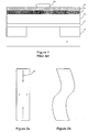
- FIG. 1 shows a structure including amorphous carbon that may be used in the formation of a MOSFET.
- the structure includes a semiconductor substrate 2 having field oxides 4 that bound source/drain regions of a MOSFET.
- a layer of a gate insulating material 6 such as SiO 2 is formed over the substrate.
- a layer of a gate conductive material 8 such as doped polysilicon is formed over the substrate and will be patterned to form a gate line of the MOSFET.
- a hardmask stack including an amorphous carbon layer 10 and a capping material layer 12 such as SiON.
- a photoresist mask 14 for defining the pattern of the gate is formed on the SiON capping material layer 12.
- a first etch is used to transfer the photoresist mask pattern to the SiON layer
- a second etch is used to transfer the SiON mask pattern to the amorphous carbon layer
- a third etch is used to remove oxide from the surface of the gate conductive layer
- a further etches are performed to etch the underlying gate conductive layer using the SiON and amorphous carbon patterns as a hardmask.
- amorphous carbon material has relatively poor selectivity with respect to the polysilicon gate conductive material during the polysilicon etch, and as a result the amorphous carbon is also etched during etching of the polysilicon, resulting in degradation of the transferred pattern.
- a proposed solution to this problem is to dope the amorphous carbon with nitrogen, which enhances its selectivity with respect to polysilicon.
- the nitrogen doping technique creates other problems that become more significant as device dimensions are reduced.
- One problem involves poisoning of the photoresist with nitrogen from the amorphous carbon layer. Poisoning is enabled by pinholes in the SiON cap layer that randomly occur during SiON deposition. The pinholes extend partly or entirely through the SiON layer, enabling nitrogen dopant from the amorphous carbon to diffuse into the photoresist. Poisoned photoresist is difficult to remove by conventional developing techniques and therefore the poisoned photoresist degrades the quality of the photoresist mask. As SiON cap layers become thinner, the poisoning problem becomes more pronounced.
- FIG. 2a shows a top view of a patterned amorphous carbon line.
- the line is subject to compressive forces 16 resulting from differences in the thermal expansion coefficients of amorphous carbon, polysilicon and SiON.
- the compressive forces along the length of the line become significantly greater than those across the width of the line. So long as a SiON top layer is present on the amorphous carbon line, the compressive forces do not deform the line.
- an etch for removing oxide from the polysilicon layer is performed after patterning the amorphous carbon, and this etch typically removes most or all of the SiON overlying the amorphous carbon line.
- the internal compressive forces of the amorphous carbon are no longer restrained, and the amorphous carbon delaminates from the underlying polysilicon and may assume a "squiggle" pattern as shown in Figure 2b that effectively lengthens the line to relieve compressive stress. This pattern will be reproduced in the polysilicon upon further etching, resulting in a deformed gate line.
- the severity of this problem is enhanced by nitrogen doping.
- a hardmask stack is comprised of alternating layers of doped amorphous carbon and undoped amorphous carbon.
- the undoped amorphous carbon layers serve as buffer layers that constrain the effects of compressive stress within the doped amorphous carbon layers to prevent delamination.
- the stack is provided with a top capping material layer.
- the layer beneath the capping material layer is preferably undoped amorphous carbon to reduce photoresist poisoning.
- a hardmask stack is comprised of alternating layers of a capping material and amorphous carbon.
- the amorphous carbon layers may be doped or undoped.
- the capping material layers serve as buffer layers that constrain the effects of compressive stress within the amorphous carbon layers to prevent delamination.
- the top layer of the stack is formed of the capping material.
- the layer beneath the capping layer is preferably undoped amorphous carbon to reduce photoresist poisoning.
- the lowest layer of the hardmask stack is preferably amorphous carbon to facilitate easy removal of the hardmask stack from the underlying materials by an ashing process.
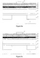
- Figures 3a and 3b show alternative structure formed in accordance with a first preferred embodiment of the invention.
- the structure of Figure 3a includes a semiconductor substrate 2 having field oxides 4 that bound source/drain regions of a MOSFET. Layers of a gate insulating material 6 such as SiO 2 and a gate conductive material 8 such as doped polysilicon are formed over the substrate and will be patterned to form a gate line and gate insulator of the MOSFET. Formed over the gate conductive layer 8 is a hardmask stack including an amorphous carbon portion formed in contact with the underlying polysilicon.
- a gate insulating material 6 such as SiO 2
- a gate conductive material 8 such as doped polysilicon
- the amorphous carbon portion is comprised of discrete alternating layers of doped amorphous carbon 22 containing dopant such as nitrogen for enhancing its etch selectivity relative to the polysilicon, and undoped amorphous carbon 20 that contains essentially none of the etch selectivity enhancing dopant of the doped layers 22.
- a capping layer 12 of SiON, silicon oxide or silicon nitride is formed over the amorphous carbon portion of the hardmask stack, and a photoresist mask 14 for defining the pattern of the gate line is formed on the capping layer 12.
- the total height of the hardmask stack is preferably approximately 50nm (500 angstroms.)
- the structure of Figure 3a differs from the structure of Figure 1 in its use of undoped amorphous carbon layers 20 in conjunction with one or more doped amorphous carbon layers 22.
- the undoped layers 20 serve as buffering layers that constrain the compressive stresses within the doped layers 22 to prevent delamination. While any number and order of doped and undoped layers may be employed in accordance with this embodiment, it is preferred to provide an uppermost layer of undoped amorphous carbon in contact with the capping layer to reduce photoresist poisoning, and to provide a lowermost layer of undoped amorphous carbon formed on the underlying polysilicon layer to increase resistance to delamination.
- the layers of the amorphous carbon portion illustrated in Figure 3a are formed as discrete layers in independent processing steps.
- the doped and undoped layers may be formed as continuous layers as illustrated in Figure 3b . This is done by varying dopant source gas flow rates during a single continuous deposition process to produce a dopant profile having a desired gradient through the amorphous carbon portion of the hardmask.
- FIG. 3a and 3b may employ a greater number of layers of doped and undoped amorphous carbon, and may arrange those layers in a different order, such as by having a doped layer formed on the underlying polysilicon.
- alternative capping materials such as silicon rich oxide, or silicon rich nitride may be employed.
- such hardmask structures may be formed over a different material to be etched, such as a metal wiring layer, or may be used to form a different type of patterned structure, such as a contact or interconnect.
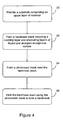
- Figure 4 shows a process flow for manufacture of a semiconductor device encompassing the first preferred embodiment, its aforementioned alternatives, and further alternative embodiments not explicitly discussed.
- a substrate comprising an upper layer of material is provided (30).
- a hardmask stack is then formed on the upper layer of material (32).
- the hardmask stack is comprised of an amorphous carbon portion formed in contact with the layer of material, and a capping layer formed on the amorphous carbon portion.
- the amorphous carbon portion is comprised of alternating layers of doped amorphous carbon containing dopant for enhancing etch selectivity with respect to the material, and undoped amorphous carbon that contains essentially none of the dopant.
- a photoresist mask is then formed over the hardmask (34).
- the photoresist mask may be trimmed by a photoresist trimming process.
- the hardmask stack is then etched using the photoresist mask as an initial etch mask to form a hardmask for patterning the underlying material (36).
- Further processing may also be performed such as patterning the upper layer of material and removing the hardmask.
- Figure 5 shows a structure formed in accordance with a second preferred embodiment of the invention.
- the structure of Figure 5 includes a semiconductor substrate 2 having field oxides 4 that bound source/drain regions of a MOSFET. Layers of a gate insulating material 6 such as silicon oxide and a gate conductive material 8 such as doped polysilicon are formed over the substrate. The gate conductive layer 8 will be patterned to form a gate line of a MOSFET. Formed over the gate conductive layer 8 is a hardmask stack including alternating layers of amorphous carbon 40 and a layer of a capping material 42 such as silicon oxide, silicon nitride, or silicon oxynitride. The amorphous carbon may be doped or undoped. A photoresist mask 14 for defining the pattern of the gate line is formed on the upper layer of capping material. The total height of the hardmask stack is preferably approximately 50nm (500 angstroms). The layers of capping material are preferably 2-5nm (20 - 50 angstroms) in height.
- the structure of Figure 5 differs from the structure of Figure 1 in its use of multiple alternating layers of amorphous carbon and capping material.
- the layers of capping material 42 serve as buffering layers that constrain compressive stresses within amorphous carbon layers 40 to prevent delamination. While the uppermost layer of capping material will typically be removed during the course of etching the hardmask, the remaining layer or layers of capping material will remain to resist delamination.
- the lowermost layer of the hardmask stack is amorphous carbon in order to enable removal of the hardmask by an ashing process, and to form the uppermost amorphous carbon layer of the hardmask stack from undoped amorphous carbon to reduce photoresist poisoning.
- the lowermost layer may be formed of a capping material, and the uppermost amorphous carbon layer may be doped.
- alternative capping materials such as silicon rich oxide, or silicon rich nitride may be employed, and different capping materials may be used in different layers within the same hardmask stack.
- such hardmask structures may be formed over a different material to be etched, such as a metal wiring layer, or may be used to form a different type of patterned structure, such as a contact or interconnect.
- Figure 6 shows a process flow for manufacture of a semiconductor device encompassing the second preferred embodiment, its aforementioned alternatives, and further alternative embodiments not explicitly discussed.
- a substrate comprising an upper layer of material is provided (50).
- a hardmask stack is then formed on the upper layer of material (52).
- the hardmask stack is comprised of alternating layers of capping material and amorphous carbon including at least a first upper layer of capping material, a layer of amorphous carbon underlying the first upper layer of capping material, and a second layer of capping material underlying the layer of amorphous carbon.
- a photoresist mask is then formed over the hardmask (54). The photoresist mask may be trimmed by a photoresist trimming process.
- the hardmask stack is then etched using the photoresist mask as an initial etch mask to form a hardmask for patterning the underlying upper layer of material (56).
- Further processing may also be performed such as patterning the underlying material and removing the hardmask.
Abstract
Description
- Embodiments of the invention relate to semiconductor fabrication, and in particular, to methods of eliminating pattern deformation in semiconductor devices.
- The use of amorphous carbon film as part of a hardmask stack for patterning MOSFET features has been found to be beneficial due to the ease with which amorphous carbon may be patterned and the high selectivity of amorphous carbon relative to typically used capping or protective materials such as silicon oxide, silicon nitride and silicon oxynitride.
Figure 1 shows a structure including amorphous carbon that may be used in the formation of a MOSFET. The structure includes asemiconductor substrate 2 havingfield oxides 4 that bound source/drain regions of a MOSFET. A layer of agate insulating material 6 such as SiO2 is formed over the substrate. A layer of a gateconductive material 8 such as doped polysilicon is formed over the substrate and will be patterned to form a gate line of the MOSFET. Formed over the gateconductive layer 8 is a hardmask stack including anamorphous carbon layer 10 and acapping material layer 12 such as SiON. Aphotoresist mask 14 for defining the pattern of the gate is formed on the SiONcapping material layer 12. During processing, a first etch is used to transfer the photoresist mask pattern to the SiON layer, a second etch is used to transfer the SiON mask pattern to the amorphous carbon layer, a third etch is used to remove oxide from the surface of the gate conductive layer, and a further etches are performed to etch the underlying gate conductive layer using the SiON and amorphous carbon patterns as a hardmask. - One problem with the structure of
Figure 1 is that the amorphous carbon material has relatively poor selectivity with respect to the polysilicon gate conductive material during the polysilicon etch, and as a result the amorphous carbon is also etched during etching of the polysilicon, resulting in degradation of the transferred pattern. A proposed solution to this problem is to dope the amorphous carbon with nitrogen, which enhances its selectivity with respect to polysilicon. - However, the nitrogen doping technique creates other problems that become more significant as device dimensions are reduced. One problem involves poisoning of the photoresist with nitrogen from the amorphous carbon layer. Poisoning is enabled by pinholes in the SiON cap layer that randomly occur during SiON deposition. The pinholes extend partly or entirely through the SiON layer, enabling nitrogen dopant from the amorphous carbon to diffuse into the photoresist. Poisoned photoresist is difficult to remove by conventional developing techniques and therefore the poisoned photoresist degrades the quality of the photoresist mask. As SiON cap layers become thinner, the poisoning problem becomes more pronounced.
- A second problem of amorphous carbon is delamination of etched amorphous carbon from the underlying polysilicon.
Figures 2a and 2b illustrate this problem.Figure 2a shows a top view of a patterned amorphous carbon line. The line is subject tocompressive forces 16 resulting from differences in the thermal expansion coefficients of amorphous carbon, polysilicon and SiON. As the width of the line decreases relative to its length, the compressive forces along the length of the line become significantly greater than those across the width of the line. So long as a SiON top layer is present on the amorphous carbon line, the compressive forces do not deform the line. However, during typical processing, an etch for removing oxide from the polysilicon layer is performed after patterning the amorphous carbon, and this etch typically removes most or all of the SiON overlying the amorphous carbon line. At that point the internal compressive forces of the amorphous carbon are no longer restrained, and the amorphous carbon delaminates from the underlying polysilicon and may assume a "squiggle" pattern as shown inFigure 2b that effectively lengthens the line to relieve compressive stress. This pattern will be reproduced in the polysilicon upon further etching, resulting in a deformed gate line. The severity of this problem is enhanced by nitrogen doping. - Consequently, there is a need for methods that reduce pattern deformation and photoresist poisoning while maintaining the desirable etch selectivity properties of nitrogen doped amorphous carbon.
- It is an object of the present invention to reduce pattern deformation in semiconductor device fabrication.
- In accordance with one preferred embodiment of the invention, a hardmask stack is comprised of alternating layers of doped amorphous carbon and undoped amorphous carbon. The undoped amorphous carbon layers serve as buffer layers that constrain the effects of compressive stress within the doped amorphous carbon layers to prevent delamination. The stack is provided with a top capping material layer. The layer beneath the capping material layer is preferably undoped amorphous carbon to reduce photoresist poisoning.
- In accordance with a second preferred embodiment, a hardmask stack is comprised of alternating layers of a capping material and amorphous carbon. The amorphous carbon layers may be doped or undoped. The capping material layers serve as buffer layers that constrain the effects of compressive stress within the amorphous carbon layers to prevent delamination. The top layer of the stack is formed of the capping material. The layer beneath the capping layer is preferably undoped amorphous carbon to reduce photoresist poisoning. The lowest layer of the hardmask stack is preferably amorphous carbon to facilitate easy removal of the hardmask stack from the underlying materials by an ashing process.
- Preferred embodiments of the invention will hereafter be described with reference to the accompanying drawings.
-
Figure 1 shows a structure formed during fabrication of a semiconductor device using an amorphous carbon layer. -
Figures 2a and 2b illustrate doped amorphous carbon line deformation. -
Figures 3a and 3b show structures formed during fabrication of a semiconductor device in accordance with a first preferred embodiment of the invention. -
Figure 4 shows a process flow encompassing the first preferred embodiment and alternative embodiments. -
Figures 5 shows a structure formed during fabrication of a semiconductor device in accordance with a second preferred embodiment of the invention. -
Figure 6 shows a process flow encompassing the second preferred embodiment and alternative embodiments. -
Figures 3a and 3b show alternative structure formed in accordance with a first preferred embodiment of the invention. - The structure of
Figure 3a includes asemiconductor substrate 2 havingfield oxides 4 that bound source/drain regions of a MOSFET. Layers of agate insulating material 6 such as SiO2 and a gateconductive material 8 such as doped polysilicon are formed over the substrate and will be patterned to form a gate line and gate insulator of the MOSFET. Formed over the gateconductive layer 8 is a hardmask stack including an amorphous carbon portion formed in contact with the underlying polysilicon. The amorphous carbon portion is comprised of discrete alternating layers of dopedamorphous carbon 22 containing dopant such as nitrogen for enhancing its etch selectivity relative to the polysilicon, and undopedamorphous carbon 20 that contains essentially none of the etch selectivity enhancing dopant of the dopedlayers 22. Acapping layer 12 of SiON, silicon oxide or silicon nitride is formed over the amorphous carbon portion of the hardmask stack, and aphotoresist mask 14 for defining the pattern of the gate line is formed on thecapping layer 12. The total height of the hardmask stack is preferably approximately 50nm (500 angstroms.) - The structure of
Figure 3a differs from the structure ofFigure 1 in its use of undopedamorphous carbon layers 20 in conjunction with one or more dopedamorphous carbon layers 22. Theundoped layers 20 serve as buffering layers that constrain the compressive stresses within the dopedlayers 22 to prevent delamination. While any number and order of doped and undoped layers may be employed in accordance with this embodiment, it is preferred to provide an uppermost layer of undoped amorphous carbon in contact with the capping layer to reduce photoresist poisoning, and to provide a lowermost layer of undoped amorphous carbon formed on the underlying polysilicon layer to increase resistance to delamination. - The layers of the amorphous carbon portion illustrated in
Figure 3a are formed as discrete layers in independent processing steps. In an alternative to the structure ofFigure 3a , the doped and undoped layers may be formed as continuous layers as illustrated inFigure 3b . This is done by varying dopant source gas flow rates during a single continuous deposition process to produce a dopant profile having a desired gradient through the amorphous carbon portion of the hardmask. - Further alternatives to the structures of
Figures 3a and 3b may employ a greater number of layers of doped and undoped amorphous carbon, and may arrange those layers in a different order, such as by having a doped layer formed on the underlying polysilicon. In further embodiments, alternative capping materials such as silicon rich oxide, or silicon rich nitride may be employed. In still further embodiments, such hardmask structures may be formed over a different material to be etched, such as a metal wiring layer, or may be used to form a different type of patterned structure, such as a contact or interconnect. -
Figure 4 shows a process flow for manufacture of a semiconductor device encompassing the first preferred embodiment, its aforementioned alternatives, and further alternative embodiments not explicitly discussed. Initially a substrate comprising an upper layer of material is provided (30). A hardmask stack is then formed on the upper layer of material (32). The hardmask stack is comprised of an amorphous carbon portion formed in contact with the layer of material, and a capping layer formed on the amorphous carbon portion. The amorphous carbon portion is comprised of alternating layers of doped amorphous carbon containing dopant for enhancing etch selectivity with respect to the material, and undoped amorphous carbon that contains essentially none of the dopant. - A photoresist mask is then formed over the hardmask (34). The photoresist mask may be trimmed by a photoresist trimming process. The hardmask stack is then etched using the photoresist mask as an initial etch mask to form a hardmask for patterning the underlying material (36).
- Further processing may also be performed such as patterning the upper layer of material and removing the hardmask.
-
Figure 5 shows a structure formed in accordance with a second preferred embodiment of the invention. - The structure of
Figure 5 includes asemiconductor substrate 2 havingfield oxides 4 that bound source/drain regions of a MOSFET. Layers of agate insulating material 6 such as silicon oxide and a gateconductive material 8 such as doped polysilicon are formed over the substrate. The gateconductive layer 8 will be patterned to form a gate line of a MOSFET. Formed over the gateconductive layer 8 is a hardmask stack including alternating layers ofamorphous carbon 40 and a layer of a cappingmaterial 42 such as silicon oxide, silicon nitride, or silicon oxynitride. The amorphous carbon may be doped or undoped. Aphotoresist mask 14 for defining the pattern of the gate line is formed on the upper layer of capping material. The total height of the hardmask stack is preferably approximately 50nm (500 angstroms). The layers of capping material are preferably 2-5nm (20 - 50 angstroms) in height. - The structure of
Figure 5 differs from the structure ofFigure 1 in its use of multiple alternating layers of amorphous carbon and capping material. The layers of cappingmaterial 42 serve as buffering layers that constrain compressive stresses within amorphous carbon layers 40 to prevent delamination. While the uppermost layer of capping material will typically be removed during the course of etching the hardmask, the remaining layer or layers of capping material will remain to resist delamination. - It is preferable to form the lowermost layer of the hardmask stack from amorphous carbon in order to enable removal of the hardmask by an ashing process, and to form the uppermost amorphous carbon layer of the hardmask stack from undoped amorphous carbon to reduce photoresist poisoning. However, in alternative embodiments the lowermost layer may be formed of a capping material, and the uppermost amorphous carbon layer may be doped. In further embodiments, alternative capping materials such as silicon rich oxide, or silicon rich nitride may be employed, and different capping materials may be used in different layers within the same hardmask stack. In still further embodiments, such hardmask structures may be formed over a different material to be etched, such as a metal wiring layer, or may be used to form a different type of patterned structure, such as a contact or interconnect.
-
Figure 6 shows a process flow for manufacture of a semiconductor device encompassing the second preferred embodiment, its aforementioned alternatives, and further alternative embodiments not explicitly discussed. Initially a substrate comprising an upper layer of material is provided (50). A hardmask stack is then formed on the upper layer of material (52). The hardmask stack is comprised of alternating layers of capping material and amorphous carbon including at least a first upper layer of capping material, a layer of amorphous carbon underlying the first upper layer of capping material, and a second layer of capping material underlying the layer of amorphous carbon. A photoresist mask is then formed over the hardmask (54). The photoresist mask may be trimmed by a photoresist trimming process. The hardmask stack is then etched using the photoresist mask as an initial etch mask to form a hardmask for patterning the underlying upper layer of material (56). - Further processing may also be performed such as patterning the underlying material and removing the hardmask.
Claims (10)
- A method for fabricating a semiconductor device comprising:providing a substrate comprising an upper layer of material (8);forming a hardmask stack on the upper layer of material, the hardmask stack comprising an amorphous carbon portion formed in contact with the layer of material (8), and a capping layer (12) formed on the amorphous carbon portion, the amorphous carbon portion comprising alternating layers of doped amorphous carbon (22) containing dopant for enhancing etch selectivity with respect to said upper layer of material, and undoped amorphous carbon (20) containing essentially none of said dopant;forming a photoresist mask (14) over the hardmask stack; andetching the hardmask stack using the photoresist mask (14) as an initial etch mask to form a hardmask for patterning said upper layer of material.
- The method claimed in claim 1, further comprising:patterning the upper layer of material (8) using the hardmask; andremoving the hardmask by an ashing process.
- The method claimed in claim 1, wherein forming said photoresist mask comprises:forming a photoresist pattern on said capping layer; andtrimming said photoresist pattern.
- A structure formed during fabrication of a semiconductor device, comprising:a substrate comprising an upper layer of material (8); anda hardmask stack formed on said upper layer of material, the hardmask stack comprising an amorphous carbon portion formed in contact with said upper layer of material, and a capping layer formed on the amorphous carbon portion, the amorphous carbon portion comprising alternating layers of doped amorphous carbon (22) containing dopant for enhancing etch selectivity with respect to the material, and undoped amorphous carbon (20) containing essentially none of said dopant.
- The structure claimed in claim 4, wherein the amorphous carbon portion of the hardmask comprises:a lowermost layer of undoped amorphous carbon (20) formed on said upper layer of material (8);an uppermost layer of undoped amorphous carbon (20) formed in contact with said capping layer (12); andat least one layer of doped amorphous carbon (22) between said uppermost (20) and lowermost (20) layers of undoped amorphous carbon.
- A method for fabricating a semiconductor device comprising:providing a substrate comprising an upper layer of material (8);forming a hardmask stack on the upper layer of material (8), the hardmask stack comprising alternating layers of capping material (42) and amorphous carbon (40) including at least an upper capping material layer (42) and a lower capping material layer (42), and at least one amorphous carbon layer (40) formed between the upper and lower capping material layers (42);forming a photoresist mask (14) over the hardmask stack; andetching the hardmask stack using the photoresist mask (14) as an initial etch mask to form a hardmask for patterning said upper layer of material (8).
- The method claimed in claim 6, wherein the hardmask stack further comprises a lower amorphous carbon layer (40) formed on said upper layer of material (8), said lower capping material layer (42) being formed on said lower amorphous carbon layer (40), and
wherein the method further comprises:patterning the upper layer of material (8) using the hardmask; andremoving the hardmask from the upper layer of material (8) by an ashing process. - The method claimed in claim 6, wherein said lower amorphous carbon layer (40) contains dopant for enhancing etch selectivity with respect to said upper layer of material (8).
- A structure formed during fabrication of a semiconductor device, comprising:a substrate comprising an upper layer of material (8); anda hardmask stack formed on said upper layer of material, the hardmask stack comprising alternating layers of capping material (42) and amorphous carbon (40) including at least an upper capping material layer (42) and a lower capping material layer (42), and at least one amorphous carbon layer (40) formed between the upper and lower capping material layers (42).
- The structure claimed in claim 9, wherein the hardmask further comprises a lower amorphous carbon layer (40) formed on said upper layer of material (8), said lower capping material layer (42) being formed on said lower amorphous carbon layer (40), and
wherein said lower amorphous carbon layer (40) contains dopant for enhancing etch selectivity with respect to said upper layer of material (8).
Applications Claiming Priority (5)
| Application Number | Priority Date | Filing Date | Title |
|---|---|---|---|
| US40045302P | 2002-07-31 | 2002-07-31 | |
| US400453P | 2002-07-31 | ||
| US10/334,392 US6764949B2 (en) | 2002-07-31 | 2002-12-30 | Method for reducing pattern deformation and photoresist poisoning in semiconductor device fabrication |
| US334392 | 2002-12-30 | ||
| PCT/US2003/023746 WO2004012246A2 (en) | 2002-07-31 | 2003-07-29 | Method for reducing pattern deformation and photoresist poisoning in semiconductor device fabrication |
Publications (2)
| Publication Number | Publication Date |
|---|---|
| EP1576657A2 EP1576657A2 (en) | 2005-09-21 |
| EP1576657B1 true EP1576657B1 (en) | 2010-01-13 |
Family
ID=31190859
Family Applications (1)
| Application Number | Title | Priority Date | Filing Date |
|---|---|---|---|
| EP03772065A Expired - Lifetime EP1576657B1 (en) | 2002-07-31 | 2003-07-29 | Method for reducing pattern deformation and photoresist poisoning in semiconductor device fabrication |
Country Status (9)
| Country | Link |
|---|---|
| US (1) | US6764949B2 (en) |
| EP (1) | EP1576657B1 (en) |
| JP (1) | JP4599578B2 (en) |
| KR (1) | KR101001346B1 (en) |
| CN (1) | CN100341114C (en) |
| AU (1) | AU2003254254A1 (en) |
| DE (1) | DE60330998D1 (en) |
| TW (1) | TWI307917B (en) |
| WO (1) | WO2004012246A2 (en) |
Families Citing this family (82)
| Publication number | Priority date | Publication date | Assignee | Title |
|---|---|---|---|---|
| US6573030B1 (en) * | 2000-02-17 | 2003-06-03 | Applied Materials, Inc. | Method for depositing an amorphous carbon layer |
| US6939808B2 (en) * | 2002-08-02 | 2005-09-06 | Applied Materials, Inc. | Undoped and fluorinated amorphous carbon film as pattern mask for metal etch |
| US7084071B1 (en) * | 2002-09-16 | 2006-08-01 | Advanced Micro Devices, Inc. | Use of multilayer amorphous carbon ARC stack to eliminate line warpage phenomenon |
| US6803313B2 (en) * | 2002-09-27 | 2004-10-12 | Advanced Micro Devices, Inc. | Method for forming a hardmask employing multiple independently formed layers of a pecvd material to reduce pinholes |
| US6855627B1 (en) * | 2002-12-04 | 2005-02-15 | Advanced Micro Devices, Inc. | Method of using amorphous carbon to prevent resist poisoning |
| US6972255B2 (en) * | 2003-07-28 | 2005-12-06 | Freescale Semiconductor, Inc. | Semiconductor device having an organic anti-reflective coating (ARC) and method therefor |
| US7129180B2 (en) * | 2003-09-12 | 2006-10-31 | Micron Technology, Inc. | Masking structure having multiple layers including an amorphous carbon layer |
| US7132201B2 (en) | 2003-09-12 | 2006-11-07 | Micron Technology, Inc. | Transparent amorphous carbon structure in semiconductor devices |
| US6838347B1 (en) * | 2003-09-23 | 2005-01-04 | International Business Machines Corporation | Method for reducing line edge roughness of oxide material using chemical oxide removal |
| US7064078B2 (en) * | 2004-01-30 | 2006-06-20 | Applied Materials | Techniques for the use of amorphous carbon (APF) for various etch and litho integration scheme |
| US7172969B2 (en) * | 2004-08-26 | 2007-02-06 | Tokyo Electron Limited | Method and system for etching a film stack |
| US7151040B2 (en) * | 2004-08-31 | 2006-12-19 | Micron Technology, Inc. | Methods for increasing photo alignment margins |
| US7910288B2 (en) | 2004-09-01 | 2011-03-22 | Micron Technology, Inc. | Mask material conversion |
| US7655387B2 (en) | 2004-09-02 | 2010-02-02 | Micron Technology, Inc. | Method to align mask patterns |
| US7115525B2 (en) * | 2004-09-02 | 2006-10-03 | Micron Technology, Inc. | Method for integrated circuit fabrication using pitch multiplication |
| US7390746B2 (en) | 2005-03-15 | 2008-06-24 | Micron Technology, Inc. | Multiple deposition for integration of spacers in pitch multiplication process |
| US7253118B2 (en) * | 2005-03-15 | 2007-08-07 | Micron Technology, Inc. | Pitch reduced patterns relative to photolithography features |
| US7611944B2 (en) * | 2005-03-28 | 2009-11-03 | Micron Technology, Inc. | Integrated circuit fabrication |
| US7120046B1 (en) | 2005-05-13 | 2006-10-10 | Micron Technology, Inc. | Memory array with surrounding gate access transistors and capacitors with global and staggered local bit lines |
| US7371627B1 (en) | 2005-05-13 | 2008-05-13 | Micron Technology, Inc. | Memory array with ultra-thin etched pillar surround gate access transistors and buried data/bit lines |
| US7429536B2 (en) | 2005-05-23 | 2008-09-30 | Micron Technology, Inc. | Methods for forming arrays of small, closely spaced features |
| US7560390B2 (en) | 2005-06-02 | 2009-07-14 | Micron Technology, Inc. | Multiple spacer steps for pitch multiplication |
| US7396781B2 (en) * | 2005-06-09 | 2008-07-08 | Micron Technology, Inc. | Method and apparatus for adjusting feature size and position |
| US7541632B2 (en) * | 2005-06-14 | 2009-06-02 | Micron Technology, Inc. | Relaxed-pitch method of aligning active area to digit line |
| US7271108B2 (en) * | 2005-06-28 | 2007-09-18 | Lam Research Corporation | Multiple mask process with etch mask stack |
| US7888721B2 (en) * | 2005-07-06 | 2011-02-15 | Micron Technology, Inc. | Surround gate access transistors with grown ultra-thin bodies |
| US7768051B2 (en) * | 2005-07-25 | 2010-08-03 | Micron Technology, Inc. | DRAM including a vertical surround gate transistor |
| US7413981B2 (en) * | 2005-07-29 | 2008-08-19 | Micron Technology, Inc. | Pitch doubled circuit layout |
| US8123968B2 (en) * | 2005-08-25 | 2012-02-28 | Round Rock Research, Llc | Multiple deposition for integration of spacers in pitch multiplication process |
| US7816262B2 (en) | 2005-08-30 | 2010-10-19 | Micron Technology, Inc. | Method and algorithm for random half pitched interconnect layout with constant spacing |
| US7829262B2 (en) * | 2005-08-31 | 2010-11-09 | Micron Technology, Inc. | Method of forming pitch multipled contacts |
| US7696567B2 (en) * | 2005-08-31 | 2010-04-13 | Micron Technology, Inc | Semiconductor memory device |
| US7393789B2 (en) * | 2005-09-01 | 2008-07-01 | Micron Technology, Inc. | Protective coating for planarization |
| US7776744B2 (en) * | 2005-09-01 | 2010-08-17 | Micron Technology, Inc. | Pitch multiplication spacers and methods of forming the same |
| US7416943B2 (en) * | 2005-09-01 | 2008-08-26 | Micron Technology, Inc. | Peripheral gate stacks and recessed array gates |
| US7687342B2 (en) * | 2005-09-01 | 2010-03-30 | Micron Technology, Inc. | Method of manufacturing a memory device |
| US7759197B2 (en) * | 2005-09-01 | 2010-07-20 | Micron Technology, Inc. | Method of forming isolated features using pitch multiplication |
| US7572572B2 (en) | 2005-09-01 | 2009-08-11 | Micron Technology, Inc. | Methods for forming arrays of small, closely spaced features |
| US7557032B2 (en) * | 2005-09-01 | 2009-07-07 | Micron Technology, Inc. | Silicided recessed silicon |
| JP2007149768A (en) * | 2005-11-24 | 2007-06-14 | Nec Electronics Corp | Method of manufacturing semiconductor device |
| US7842558B2 (en) * | 2006-03-02 | 2010-11-30 | Micron Technology, Inc. | Masking process for simultaneously patterning separate regions |
| US7476933B2 (en) * | 2006-03-02 | 2009-01-13 | Micron Technology, Inc. | Vertical gated access transistor |
| US7902074B2 (en) | 2006-04-07 | 2011-03-08 | Micron Technology, Inc. | Simplified pitch doubling process flow |
| US8003310B2 (en) | 2006-04-24 | 2011-08-23 | Micron Technology, Inc. | Masking techniques and templates for dense semiconductor fabrication |
| US7488685B2 (en) | 2006-04-25 | 2009-02-10 | Micron Technology, Inc. | Process for improving critical dimension uniformity of integrated circuit arrays |
| US7795149B2 (en) | 2006-06-01 | 2010-09-14 | Micron Technology, Inc. | Masking techniques and contact imprint reticles for dense semiconductor fabrication |
| US7723009B2 (en) | 2006-06-02 | 2010-05-25 | Micron Technology, Inc. | Topography based patterning |
| US7611980B2 (en) | 2006-08-30 | 2009-11-03 | Micron Technology, Inc. | Single spacer process for multiplying pitch by a factor greater than two and related intermediate IC structures |
| US7517804B2 (en) * | 2006-08-31 | 2009-04-14 | Micron Technologies, Inc. | Selective etch chemistries for forming high aspect ratio features and associated structures |
| US7666578B2 (en) | 2006-09-14 | 2010-02-23 | Micron Technology, Inc. | Efficient pitch multiplication process |
| KR100772706B1 (en) | 2006-09-28 | 2007-11-02 | 주식회사 하이닉스반도체 | Method for fabricating contact in semiconductor device |
| KR100834396B1 (en) * | 2006-12-27 | 2008-06-04 | 주식회사 하이닉스반도체 | Method for forming a pattern in semiconductor device |
| KR100808056B1 (en) * | 2006-12-27 | 2008-02-28 | 주식회사 하이닉스반도체 | Method for forming pattern using hardmask |
| KR100792405B1 (en) * | 2007-01-03 | 2008-01-09 | 주식회사 하이닉스반도체 | Method for fabricating bulb type recess pattern |
| US20080254233A1 (en) * | 2007-04-10 | 2008-10-16 | Kwangduk Douglas Lee | Plasma-induced charge damage control for plasma enhanced chemical vapor deposition processes |
| US9732416B1 (en) | 2007-04-18 | 2017-08-15 | Novellus Systems, Inc. | Wafer chuck with aerodynamic design for turbulence reduction |
| US7923373B2 (en) | 2007-06-04 | 2011-04-12 | Micron Technology, Inc. | Pitch multiplication using self-assembling materials |
| US7718546B2 (en) * | 2007-06-27 | 2010-05-18 | Sandisk 3D Llc | Method for fabricating a 3-D integrated circuit using a hard mask of silicon-oxynitride on amorphous carbon |
| US8563229B2 (en) * | 2007-07-31 | 2013-10-22 | Micron Technology, Inc. | Process of semiconductor fabrication with mask overlay on pitch multiplied features and associated structures |
| US20090098701A1 (en) * | 2007-10-15 | 2009-04-16 | Jurgen Faul | Method of manufacturing an integrated circuit |
| US7737039B2 (en) | 2007-11-01 | 2010-06-15 | Micron Technology, Inc. | Spacer process for on pitch contacts and related structures |
| US7659208B2 (en) | 2007-12-06 | 2010-02-09 | Micron Technology, Inc | Method for forming high density patterns |
| US7790531B2 (en) * | 2007-12-18 | 2010-09-07 | Micron Technology, Inc. | Methods for isolating portions of a loop of pitch-multiplied material and related structures |
| US8030218B2 (en) | 2008-03-21 | 2011-10-04 | Micron Technology, Inc. | Method for selectively modifying spacing between pitch multiplied structures |
| US8110476B2 (en) * | 2008-04-11 | 2012-02-07 | Sandisk 3D Llc | Memory cell that includes a carbon-based memory element and methods of forming the same |
| US8076208B2 (en) | 2008-07-03 | 2011-12-13 | Micron Technology, Inc. | Method for forming transistor with high breakdown voltage using pitch multiplication technique |
| US8557685B2 (en) * | 2008-08-07 | 2013-10-15 | Sandisk 3D Llc | Memory cell that includes a carbon-based memory element and methods of forming the same |
| US8419964B2 (en) | 2008-08-27 | 2013-04-16 | Novellus Systems, Inc. | Apparatus and method for edge bevel removal of copper from silicon wafers |
| US8101497B2 (en) | 2008-09-11 | 2012-01-24 | Micron Technology, Inc. | Self-aligned trench formation |
| US8492282B2 (en) * | 2008-11-24 | 2013-07-23 | Micron Technology, Inc. | Methods of forming a masking pattern for integrated circuits |
| US8172646B2 (en) | 2009-02-27 | 2012-05-08 | Novellus Systems, Inc. | Magnetically actuated chuck for edge bevel removal |
| US8304175B2 (en) * | 2009-03-25 | 2012-11-06 | Macronix International Co., Ltd. | Patterning method |
| TWI419201B (en) * | 2009-04-27 | 2013-12-11 | Macronix Int Co Ltd | Patterning method |
| DE102009046259B4 (en) | 2009-10-30 | 2019-10-10 | GLOBALFOUNDRIES Dresden Module One Ltd. Liability Company & Co. KG | Greater adhesion of a PECVD carbon to dielectric materials by providing a bond interface |
| US8252699B2 (en) * | 2010-11-22 | 2012-08-28 | Applied Materials, Inc. | Composite removable hardmask |
| KR20130075158A (en) | 2011-12-27 | 2013-07-05 | 삼성전자주식회사 | Methods of manufacturing a semiconductor device |
| US9881788B2 (en) | 2014-05-22 | 2018-01-30 | Lam Research Corporation | Back side deposition apparatus and applications |
| KR102477091B1 (en) * | 2015-07-24 | 2022-12-13 | 삼성전자주식회사 | Two-dimensional material hard mask, method of manufacturing the same and method of forming pattern of material layer using hard mask |
| US9806161B1 (en) * | 2016-04-07 | 2017-10-31 | Globalfoundries Inc. | Integrated circuit structure having thin gate dielectric device and thick gate dielectric device |
| CN108695162B (en) | 2017-04-12 | 2021-04-09 | 联华电子股份有限公司 | Method for manufacturing fin structure |
| US10345702B2 (en) | 2017-08-24 | 2019-07-09 | International Business Machines Corporation | Polymer brushes for extreme ultraviolet photolithography |
| US10522750B2 (en) | 2018-02-19 | 2019-12-31 | Taiwan Semiconductor Manufacturing Company, Ltd. | Multiply spin-coated ultra-thick hybrid hard mask for sub 60nm MRAM devices |
Family Cites Families (9)
| Publication number | Priority date | Publication date | Assignee | Title |
|---|---|---|---|---|
| EP0517627A1 (en) * | 1991-06-07 | 1992-12-09 | Eastman Kodak Company | Deposited carbon mask for dry etch processing of Si |
| FR2687844A1 (en) * | 1992-02-26 | 1993-08-27 | Chouan Yannick | PROCESS FOR PRODUCING A DUAL GRID THIN FILM TRANSISTOR AND OPTICAL MASK |
| KR100188508B1 (en) * | 1993-03-26 | 1999-06-01 | 세끼사와 다까시 | Reduction of reflection by amorphous carbon |
| US5759746A (en) * | 1996-05-24 | 1998-06-02 | Kabushiki Kaisha Toshiba | Fabrication process using a thin resist |
| JP3047832B2 (en) * | 1996-10-03 | 2000-06-05 | 日本電気株式会社 | Method for manufacturing semiconductor device |
| US6143476A (en) * | 1997-12-12 | 2000-11-07 | Applied Materials Inc | Method for high temperature etching of patterned layers using an organic mask stack |
| TWI246633B (en) * | 1997-12-12 | 2006-01-01 | Applied Materials Inc | Method of pattern etching a low k dielectric layen |
| JP2000058830A (en) * | 1998-05-28 | 2000-02-25 | Texas Instr Inc <Ti> | Antireflection structure and manufacture thereof |
| US6664639B2 (en) * | 2000-12-22 | 2003-12-16 | Matrix Semiconductor, Inc. | Contact and via structure and method of fabrication |
-
2002
- 2002-12-30 US US10/334,392 patent/US6764949B2/en not_active Expired - Lifetime
-
2003
- 2003-07-29 AU AU2003254254A patent/AU2003254254A1/en not_active Abandoned
- 2003-07-29 CN CNB038182580A patent/CN100341114C/en not_active Expired - Lifetime
- 2003-07-29 DE DE60330998T patent/DE60330998D1/en not_active Expired - Lifetime
- 2003-07-29 WO PCT/US2003/023746 patent/WO2004012246A2/en active Application Filing
- 2003-07-29 JP JP2004525039A patent/JP4599578B2/en not_active Expired - Fee Related
- 2003-07-29 EP EP03772065A patent/EP1576657B1/en not_active Expired - Lifetime
- 2003-07-29 KR KR1020057000968A patent/KR101001346B1/en not_active IP Right Cessation
- 2003-07-31 TW TW092120947A patent/TWI307917B/en not_active IP Right Cessation
Also Published As
| Publication number | Publication date |
|---|---|
| EP1576657A2 (en) | 2005-09-21 |
| WO2004012246A3 (en) | 2004-05-13 |
| WO2004012246A2 (en) | 2004-02-05 |
| CN100341114C (en) | 2007-10-03 |
| TWI307917B (en) | 2009-03-21 |
| US6764949B2 (en) | 2004-07-20 |
| KR101001346B1 (en) | 2010-12-14 |
| CN1672243A (en) | 2005-09-21 |
| AU2003254254A1 (en) | 2004-02-16 |
| KR20050019905A (en) | 2005-03-03 |
| TW200405414A (en) | 2004-04-01 |
| US20040023475A1 (en) | 2004-02-05 |
| JP2005535119A (en) | 2005-11-17 |
| DE60330998D1 (en) | 2010-03-04 |
| JP4599578B2 (en) | 2010-12-15 |
Similar Documents
| Publication | Publication Date | Title |
|---|---|---|
| EP1576657B1 (en) | Method for reducing pattern deformation and photoresist poisoning in semiconductor device fabrication | |
| US5872385A (en) | Conductive interconnect structure and method of formation | |
| US7892940B2 (en) | Device and methodology for reducing effective dielectric constant in semiconductor devices | |
| US7183198B2 (en) | Method for forming a hardmask employing multiple independently formed layers of a capping material to reduce pinholes | |
| US6750127B1 (en) | Method for fabricating a semiconductor device using amorphous carbon having improved etch resistance | |
| US6828219B2 (en) | Stacked spacer structure and process | |
| KR100190261B1 (en) | Method of fabricating gate stack having a reduced height | |
| JPH0817930A (en) | Semiconductor device structure using etching stop layer and its method | |
| US6849530B2 (en) | Method for semiconductor gate line dimension reduction | |
| US5512518A (en) | Method of manufacture of multilayer dielectric on a III-V substrate | |
| US6218311B1 (en) | Post-etch treatment of a semiconductor device | |
| US6764947B1 (en) | Method for reducing gate line deformation and reducing gate line widths in semiconductor devices | |
| JP4989817B2 (en) | Semiconductor device and manufacturing method thereof | |
| KR20080092614A (en) | Method of fabricating semiconductor device | |
| KR100875653B1 (en) | Method of forming fine pattern of semiconductor device | |
| KR100505407B1 (en) | Method of etching hard mask layer in semiconductor device | |
| US7268066B2 (en) | Method for semiconductor gate line dimension reduction | |
| KR100500457B1 (en) | A Semiconductor Device Having A Pocket Line and Fabrication Method Thereof | |
| US6828082B2 (en) | Method to pattern small features by using a re-flowable hard mask | |
| KR100226767B1 (en) | Method of manufacturing semiconductor device | |
| KR100447989B1 (en) | Gate electrode formation method of semiconductor device | |
| KR101026371B1 (en) | Method for forming Gate | |
| KR100412137B1 (en) | Method for forming gate spacer of semiconductor device | |
| KR100800106B1 (en) | Method for forming trench isolation layer in semiconductor device | |
| US20040185608A1 (en) | Methods of forming integrated circuit devices using buffer layers covering conductive/insulating interfaces |
Legal Events
| Date | Code | Title | Description |
|---|---|---|---|
| PUAI | Public reference made under article 153(3) epc to a published international application that has entered the european phase |
Free format text: ORIGINAL CODE: 0009012 |
|
| 17P | Request for examination filed |
Effective date: 20050114 |
|
| AK | Designated contracting states |
Kind code of ref document: A2 Designated state(s): AT BE BG CH CY CZ DE DK EE ES FI FR GB GR HU IE IT LI LU MC NL PT RO SE SI SK TR |
|
| AX | Request for extension of the european patent |
Extension state: AL LT LV MK |
|
| DAX | Request for extension of the european patent (deleted) | ||
| RBV | Designated contracting states (corrected) |
Designated state(s): DE FR GB |
|
| RIC1 | Information provided on ipc code assigned before grant |
Ipc: H01L 21/3213 20060101ALI20090401BHEP Ipc: H01L 21/033 20060101AFI20090401BHEP |
|
| GRAP | Despatch of communication of intention to grant a patent |
Free format text: ORIGINAL CODE: EPIDOSNIGR1 |
|
| GRAS | Grant fee paid |
Free format text: ORIGINAL CODE: EPIDOSNIGR3 |
|
| GRAA | (expected) grant |
Free format text: ORIGINAL CODE: 0009210 |
|
| RAP1 | Party data changed (applicant data changed or rights of an application transferred) |
Owner name: GLOBALFOUNDRIES, INC. |
|
| AK | Designated contracting states |
Kind code of ref document: B1 Designated state(s): DE FR GB |
|
| REG | Reference to a national code |
Ref country code: GB Ref legal event code: FG4D |
|
| REF | Corresponds to: |
Ref document number: 60330998 Country of ref document: DE Date of ref document: 20100304 Kind code of ref document: P |
|
| PLBE | No opposition filed within time limit |
Free format text: ORIGINAL CODE: 0009261 |
|
| STAA | Information on the status of an ep patent application or granted ep patent |
Free format text: STATUS: NO OPPOSITION FILED WITHIN TIME LIMIT |
|
| PGFP | Annual fee paid to national office [announced via postgrant information from national office to epo] |
Ref country code: GB Payment date: 20100616 Year of fee payment: 8 |
|
| 26N | No opposition filed |
Effective date: 20101014 |
|
| REG | Reference to a national code |
Ref country code: FR Ref legal event code: ST Effective date: 20110331 |
|
| PG25 | Lapsed in a contracting state [announced via postgrant information from national office to epo] |
Ref country code: FR Free format text: LAPSE BECAUSE OF NON-PAYMENT OF DUE FEES Effective date: 20100802 |
|
| PGFP | Annual fee paid to national office [announced via postgrant information from national office to epo] |
Ref country code: DE Payment date: 20110727 Year of fee payment: 9 |
|
| GBPC | Gb: european patent ceased through non-payment of renewal fee |
Effective date: 20110729 |
|
| PG25 | Lapsed in a contracting state [announced via postgrant information from national office to epo] |
Ref country code: GB Free format text: LAPSE BECAUSE OF NON-PAYMENT OF DUE FEES Effective date: 20110729 |
|
| PG25 | Lapsed in a contracting state [announced via postgrant information from national office to epo] |
Ref country code: DE Free format text: LAPSE BECAUSE OF NON-PAYMENT OF DUE FEES Effective date: 20130201 |
|
| REG | Reference to a national code |
Ref country code: DE Ref legal event code: R119 Ref document number: 60330998 Country of ref document: DE Effective date: 20130201 |