EP1583159A2 - Semiconductor light emitting device capable of suppressing silver migration of reflection film made of silver - Google Patents
Semiconductor light emitting device capable of suppressing silver migration of reflection film made of silver Download PDFInfo
- Publication number
- EP1583159A2 EP1583159A2 EP04024366A EP04024366A EP1583159A2 EP 1583159 A2 EP1583159 A2 EP 1583159A2 EP 04024366 A EP04024366 A EP 04024366A EP 04024366 A EP04024366 A EP 04024366A EP 1583159 A2 EP1583159 A2 EP 1583159A2
- Authority
- EP
- European Patent Office
- Prior art keywords
- layer
- side electrode
- light emitting
- emitting device
- semiconductor light
- Prior art date
- Legal status (The legal status is an assumption and is not a legal conclusion. Google has not performed a legal analysis and makes no representation as to the accuracy of the status listed.)
- Granted
Links
- 239000004065 semiconductor Substances 0.000 title claims abstract description 89
- BQCADISMDOOEFD-UHFFFAOYSA-N Silver Chemical compound [Ag] BQCADISMDOOEFD-UHFFFAOYSA-N 0.000 title claims abstract description 16
- 229910052709 silver Inorganic materials 0.000 title claims abstract description 16
- 239000004332 silver Substances 0.000 title claims abstract description 15
- 238000013508 migration Methods 0.000 title description 19
- 230000005012 migration Effects 0.000 title description 19
- 150000004767 nitrides Chemical class 0.000 claims abstract description 15
- 238000003475 lamination Methods 0.000 claims abstract description 12
- 239000000956 alloy Substances 0.000 claims abstract description 5
- 229910045601 alloy Inorganic materials 0.000 claims abstract description 5
- VYPSYNLAJGMNEJ-UHFFFAOYSA-N Silicium dioxide Chemical compound O=[Si]=O VYPSYNLAJGMNEJ-UHFFFAOYSA-N 0.000 claims description 15
- 229910052751 metal Inorganic materials 0.000 claims description 15
- 239000002184 metal Substances 0.000 claims description 15
- 239000010936 titanium Substances 0.000 claims description 15
- 230000001681 protective effect Effects 0.000 claims description 12
- 239000000463 material Substances 0.000 claims description 11
- 229910052814 silicon oxide Inorganic materials 0.000 claims description 11
- 229910052759 nickel Inorganic materials 0.000 claims description 8
- 229910052703 rhodium Inorganic materials 0.000 claims description 7
- PNEYBMLMFCGWSK-UHFFFAOYSA-N aluminium oxide Inorganic materials [O-2].[O-2].[O-2].[Al+3].[Al+3] PNEYBMLMFCGWSK-UHFFFAOYSA-N 0.000 claims description 6
- RVTZCBVAJQQJTK-UHFFFAOYSA-N oxygen(2-);zirconium(4+) Chemical compound [O-2].[O-2].[Zr+4] RVTZCBVAJQQJTK-UHFFFAOYSA-N 0.000 claims description 6
- 229910052719 titanium Inorganic materials 0.000 claims description 6
- 229910001928 zirconium oxide Inorganic materials 0.000 claims description 6
- 238000004020 luminiscence type Methods 0.000 claims description 5
- 229910052750 molybdenum Inorganic materials 0.000 claims description 5
- 229910052697 platinum Inorganic materials 0.000 claims description 5
- 229910052721 tungsten Inorganic materials 0.000 claims description 5
- GWEVSGVZZGPLCZ-UHFFFAOYSA-N Titan oxide Chemical compound O=[Ti]=O GWEVSGVZZGPLCZ-UHFFFAOYSA-N 0.000 claims description 4
- 229910052782 aluminium Inorganic materials 0.000 claims description 4
- BPUBBGLMJRNUCC-UHFFFAOYSA-N oxygen(2-);tantalum(5+) Chemical compound [O-2].[O-2].[O-2].[O-2].[O-2].[Ta+5].[Ta+5] BPUBBGLMJRNUCC-UHFFFAOYSA-N 0.000 claims description 4
- 229910052763 palladium Inorganic materials 0.000 claims description 3
- 230000001902 propagating effect Effects 0.000 claims description 2
- 229910000449 hafnium oxide Inorganic materials 0.000 claims 2
- WIHZLLGSGQNAGK-UHFFFAOYSA-N hafnium(4+);oxygen(2-) Chemical compound [O-2].[O-2].[Hf+4] WIHZLLGSGQNAGK-UHFFFAOYSA-N 0.000 claims 2
- 229910001936 tantalum oxide Inorganic materials 0.000 claims 2
- OGIDPMRJRNCKJF-UHFFFAOYSA-N titanium oxide Inorganic materials [Ti]=O OGIDPMRJRNCKJF-UHFFFAOYSA-N 0.000 claims 2
- 239000010410 layer Substances 0.000 description 168
- 239000010408 film Substances 0.000 description 159
- 239000000758 substrate Substances 0.000 description 44
- 239000010931 gold Substances 0.000 description 18
- BASFCYQUMIYNBI-UHFFFAOYSA-N platinum Chemical compound [Pt] BASFCYQUMIYNBI-UHFFFAOYSA-N 0.000 description 18
- 239000010948 rhodium Substances 0.000 description 12
- 238000004088 simulation Methods 0.000 description 10
- 238000011156 evaluation Methods 0.000 description 9
- 229910052594 sapphire Inorganic materials 0.000 description 9
- 239000010980 sapphire Substances 0.000 description 9
- 238000000034 method Methods 0.000 description 6
- PCHJSUWPFVWCPO-UHFFFAOYSA-N gold Chemical compound [Au] PCHJSUWPFVWCPO-UHFFFAOYSA-N 0.000 description 5
- -1 Ag+ ions Chemical class 0.000 description 4
- KDLHZDBZIXYQEI-UHFFFAOYSA-N Palladium Chemical compound [Pd] KDLHZDBZIXYQEI-UHFFFAOYSA-N 0.000 description 4
- 230000008859 change Effects 0.000 description 4
- 230000000052 comparative effect Effects 0.000 description 4
- 238000010894 electron beam technology Methods 0.000 description 4
- 238000005530 etching Methods 0.000 description 4
- 239000011347 resin Substances 0.000 description 4
- 229920005989 resin Polymers 0.000 description 4
- 238000001771 vacuum deposition Methods 0.000 description 4
- 238000000137 annealing Methods 0.000 description 3
- 229910052737 gold Inorganic materials 0.000 description 3
- 238000005259 measurement Methods 0.000 description 3
- 230000008569 process Effects 0.000 description 3
- 238000007789 sealing Methods 0.000 description 3
- NDVLTYZPCACLMA-UHFFFAOYSA-N silver oxide Substances [O-2].[Ag+].[Ag+] NDVLTYZPCACLMA-UHFFFAOYSA-N 0.000 description 3
- 239000002344 surface layer Substances 0.000 description 3
- 238000012360 testing method Methods 0.000 description 3
- 229910002704 AlGaN Inorganic materials 0.000 description 2
- 239000004642 Polyimide Substances 0.000 description 2
- 229910052681 coesite Inorganic materials 0.000 description 2
- 229910052593 corundum Inorganic materials 0.000 description 2
- 229910052906 cristobalite Inorganic materials 0.000 description 2
- 230000005684 electric field Effects 0.000 description 2
- 238000002474 experimental method Methods 0.000 description 2
- CJNBYAVZURUTKZ-UHFFFAOYSA-N hafnium(iv) oxide Chemical compound O=[Hf]=O CJNBYAVZURUTKZ-UHFFFAOYSA-N 0.000 description 2
- 239000011810 insulating material Substances 0.000 description 2
- 230000003287 optical effect Effects 0.000 description 2
- 229920001721 polyimide Polymers 0.000 description 2
- 230000000717 retained effect Effects 0.000 description 2
- MHOVAHRLVXNVSD-UHFFFAOYSA-N rhodium atom Chemical compound [Rh] MHOVAHRLVXNVSD-UHFFFAOYSA-N 0.000 description 2
- 239000000377 silicon dioxide Substances 0.000 description 2
- 229910001923 silver oxide Inorganic materials 0.000 description 2
- 229910000108 silver(I,III) oxide Inorganic materials 0.000 description 2
- UKHWJBVVWVYFEY-UHFFFAOYSA-M silver;hydroxide Chemical compound [OH-].[Ag+] UKHWJBVVWVYFEY-UHFFFAOYSA-M 0.000 description 2
- 238000004544 sputter deposition Methods 0.000 description 2
- 229910052682 stishovite Inorganic materials 0.000 description 2
- 230000001629 suppression Effects 0.000 description 2
- 229910052905 tridymite Inorganic materials 0.000 description 2
- 229910001845 yogo sapphire Inorganic materials 0.000 description 2
- 239000000853 adhesive Substances 0.000 description 1
- 230000001070 adhesive effect Effects 0.000 description 1
- 239000000969 carrier Substances 0.000 description 1
- 238000006243 chemical reaction Methods 0.000 description 1
- 239000004020 conductor Substances 0.000 description 1
- 238000005260 corrosion Methods 0.000 description 1
- 230000007797 corrosion Effects 0.000 description 1
- 230000001419 dependent effect Effects 0.000 description 1
- 230000005611 electricity Effects 0.000 description 1
- 238000009791 electrochemical migration reaction Methods 0.000 description 1
- 229910052739 hydrogen Inorganic materials 0.000 description 1
- 239000001257 hydrogen Substances 0.000 description 1
- 125000004435 hydrogen atom Chemical class [H]* 0.000 description 1
- 238000002347 injection Methods 0.000 description 1
- 239000007924 injection Substances 0.000 description 1
- 238000004519 manufacturing process Methods 0.000 description 1
- 230000007246 mechanism Effects 0.000 description 1
- 150000002739 metals Chemical class 0.000 description 1
- 239000000203 mixture Substances 0.000 description 1
- 238000012986 modification Methods 0.000 description 1
- 230000004048 modification Effects 0.000 description 1
- 230000001590 oxidative effect Effects 0.000 description 1
- 238000001020 plasma etching Methods 0.000 description 1
- 230000000644 propagated effect Effects 0.000 description 1
- 230000005855 radiation Effects 0.000 description 1
- 230000000191 radiation effect Effects 0.000 description 1
- 238000000926 separation method Methods 0.000 description 1
- 238000005476 soldering Methods 0.000 description 1
- 230000003746 surface roughness Effects 0.000 description 1
- 239000010409 thin film Substances 0.000 description 1
- 239000012808 vapor phase Substances 0.000 description 1
- 230000000007 visual effect Effects 0.000 description 1
Images


Classifications
-
- H—ELECTRICITY
- H01—ELECTRIC ELEMENTS
- H01L—SEMICONDUCTOR DEVICES NOT COVERED BY CLASS H10
- H01L33/00—Semiconductor devices with at least one potential-jump barrier or surface barrier specially adapted for light emission; Processes or apparatus specially adapted for the manufacture or treatment thereof or of parts thereof; Details thereof
- H01L33/36—Semiconductor devices with at least one potential-jump barrier or surface barrier specially adapted for light emission; Processes or apparatus specially adapted for the manufacture or treatment thereof or of parts thereof; Details thereof characterised by the electrodes
- H01L33/40—Materials therefor
-
- H—ELECTRICITY
- H01—ELECTRIC ELEMENTS
- H01L—SEMICONDUCTOR DEVICES NOT COVERED BY CLASS H10
- H01L33/00—Semiconductor devices with at least one potential-jump barrier or surface barrier specially adapted for light emission; Processes or apparatus specially adapted for the manufacture or treatment thereof or of parts thereof; Details thereof
- H01L33/44—Semiconductor devices with at least one potential-jump barrier or surface barrier specially adapted for light emission; Processes or apparatus specially adapted for the manufacture or treatment thereof or of parts thereof; Details thereof characterised by the coatings, e.g. passivation layer or anti-reflective coating
- H01L33/46—Reflective coating, e.g. dielectric Bragg reflector
-
- H—ELECTRICITY
- H01—ELECTRIC ELEMENTS
- H01L—SEMICONDUCTOR DEVICES NOT COVERED BY CLASS H10
- H01L2224/00—Indexing scheme for arrangements for connecting or disconnecting semiconductor or solid-state bodies and methods related thereto as covered by H01L24/00
- H01L2224/01—Means for bonding being attached to, or being formed on, the surface to be connected, e.g. chip-to-package, die-attach, "first-level" interconnects; Manufacturing methods related thereto
- H01L2224/02—Bonding areas; Manufacturing methods related thereto
- H01L2224/0212—Auxiliary members for bonding areas, e.g. spacers
- H01L2224/02122—Auxiliary members for bonding areas, e.g. spacers being formed on the semiconductor or solid-state body
- H01L2224/02163—Auxiliary members for bonding areas, e.g. spacers being formed on the semiconductor or solid-state body on the bonding area
- H01L2224/02165—Reinforcing structures
- H01L2224/02166—Collar structures
-
- H—ELECTRICITY
- H01—ELECTRIC ELEMENTS
- H01L—SEMICONDUCTOR DEVICES NOT COVERED BY CLASS H10
- H01L2224/00—Indexing scheme for arrangements for connecting or disconnecting semiconductor or solid-state bodies and methods related thereto as covered by H01L24/00
- H01L2224/01—Means for bonding being attached to, or being formed on, the surface to be connected, e.g. chip-to-package, die-attach, "first-level" interconnects; Manufacturing methods related thereto
- H01L2224/02—Bonding areas; Manufacturing methods related thereto
- H01L2224/04—Structure, shape, material or disposition of the bonding areas prior to the connecting process
- H01L2224/06—Structure, shape, material or disposition of the bonding areas prior to the connecting process of a plurality of bonding areas
- H01L2224/0601—Structure
- H01L2224/0603—Bonding areas having different sizes, e.g. different heights or widths
-
- H—ELECTRICITY
- H01—ELECTRIC ELEMENTS
- H01L—SEMICONDUCTOR DEVICES NOT COVERED BY CLASS H10
- H01L2224/00—Indexing scheme for arrangements for connecting or disconnecting semiconductor or solid-state bodies and methods related thereto as covered by H01L24/00
- H01L2224/01—Means for bonding being attached to, or being formed on, the surface to be connected, e.g. chip-to-package, die-attach, "first-level" interconnects; Manufacturing methods related thereto
- H01L2224/10—Bump connectors; Manufacturing methods related thereto
- H01L2224/15—Structure, shape, material or disposition of the bump connectors after the connecting process
- H01L2224/16—Structure, shape, material or disposition of the bump connectors after the connecting process of an individual bump connector
- H01L2224/161—Disposition
- H01L2224/16135—Disposition the bump connector connecting between different semiconductor or solid-state bodies, i.e. chip-to-chip
- H01L2224/16145—Disposition the bump connector connecting between different semiconductor or solid-state bodies, i.e. chip-to-chip the bodies being stacked
-
- H—ELECTRICITY
- H01—ELECTRIC ELEMENTS
- H01L—SEMICONDUCTOR DEVICES NOT COVERED BY CLASS H10
- H01L2224/00—Indexing scheme for arrangements for connecting or disconnecting semiconductor or solid-state bodies and methods related thereto as covered by H01L24/00
- H01L2224/01—Means for bonding being attached to, or being formed on, the surface to be connected, e.g. chip-to-package, die-attach, "first-level" interconnects; Manufacturing methods related thereto
- H01L2224/42—Wire connectors; Manufacturing methods related thereto
- H01L2224/44—Structure, shape, material or disposition of the wire connectors prior to the connecting process
- H01L2224/45—Structure, shape, material or disposition of the wire connectors prior to the connecting process of an individual wire connector
- H01L2224/45001—Core members of the connector
- H01L2224/45099—Material
- H01L2224/451—Material with a principal constituent of the material being a metal or a metalloid, e.g. boron (B), silicon (Si), germanium (Ge), arsenic (As), antimony (Sb), tellurium (Te) and polonium (Po), and alloys thereof
- H01L2224/45138—Material with a principal constituent of the material being a metal or a metalloid, e.g. boron (B), silicon (Si), germanium (Ge), arsenic (As), antimony (Sb), tellurium (Te) and polonium (Po), and alloys thereof the principal constituent melting at a temperature of greater than or equal to 950°C and less than 1550°C
- H01L2224/45144—Gold (Au) as principal constituent
-
- H—ELECTRICITY
- H01—ELECTRIC ELEMENTS
- H01L—SEMICONDUCTOR DEVICES NOT COVERED BY CLASS H10
- H01L2224/00—Indexing scheme for arrangements for connecting or disconnecting semiconductor or solid-state bodies and methods related thereto as covered by H01L24/00
- H01L2224/01—Means for bonding being attached to, or being formed on, the surface to be connected, e.g. chip-to-package, die-attach, "first-level" interconnects; Manufacturing methods related thereto
- H01L2224/42—Wire connectors; Manufacturing methods related thereto
- H01L2224/47—Structure, shape, material or disposition of the wire connectors after the connecting process
- H01L2224/48—Structure, shape, material or disposition of the wire connectors after the connecting process of an individual wire connector
- H01L2224/4805—Shape
- H01L2224/4809—Loop shape
- H01L2224/48091—Arched
-
- H—ELECTRICITY
- H01—ELECTRIC ELEMENTS
- H01L—SEMICONDUCTOR DEVICES NOT COVERED BY CLASS H10
- H01L2224/00—Indexing scheme for arrangements for connecting or disconnecting semiconductor or solid-state bodies and methods related thereto as covered by H01L24/00
- H01L2224/01—Means for bonding being attached to, or being formed on, the surface to be connected, e.g. chip-to-package, die-attach, "first-level" interconnects; Manufacturing methods related thereto
- H01L2224/42—Wire connectors; Manufacturing methods related thereto
- H01L2224/47—Structure, shape, material or disposition of the wire connectors after the connecting process
- H01L2224/48—Structure, shape, material or disposition of the wire connectors after the connecting process of an individual wire connector
- H01L2224/481—Disposition
- H01L2224/48151—Connecting between a semiconductor or solid-state body and an item not being a semiconductor or solid-state body, e.g. chip-to-substrate, chip-to-passive
- H01L2224/48221—Connecting between a semiconductor or solid-state body and an item not being a semiconductor or solid-state body, e.g. chip-to-substrate, chip-to-passive the body and the item being stacked
- H01L2224/48245—Connecting between a semiconductor or solid-state body and an item not being a semiconductor or solid-state body, e.g. chip-to-substrate, chip-to-passive the body and the item being stacked the item being metallic
- H01L2224/48247—Connecting between a semiconductor or solid-state body and an item not being a semiconductor or solid-state body, e.g. chip-to-substrate, chip-to-passive the body and the item being stacked the item being metallic connecting the wire to a bond pad of the item
-
- H—ELECTRICITY
- H01—ELECTRIC ELEMENTS
- H01L—SEMICONDUCTOR DEVICES NOT COVERED BY CLASS H10
- H01L2224/00—Indexing scheme for arrangements for connecting or disconnecting semiconductor or solid-state bodies and methods related thereto as covered by H01L24/00
- H01L2224/01—Means for bonding being attached to, or being formed on, the surface to be connected, e.g. chip-to-package, die-attach, "first-level" interconnects; Manufacturing methods related thereto
- H01L2224/42—Wire connectors; Manufacturing methods related thereto
- H01L2224/47—Structure, shape, material or disposition of the wire connectors after the connecting process
- H01L2224/48—Structure, shape, material or disposition of the wire connectors after the connecting process of an individual wire connector
- H01L2224/481—Disposition
- H01L2224/48151—Connecting between a semiconductor or solid-state body and an item not being a semiconductor or solid-state body, e.g. chip-to-substrate, chip-to-passive
- H01L2224/48221—Connecting between a semiconductor or solid-state body and an item not being a semiconductor or solid-state body, e.g. chip-to-substrate, chip-to-passive the body and the item being stacked
- H01L2224/48245—Connecting between a semiconductor or solid-state body and an item not being a semiconductor or solid-state body, e.g. chip-to-substrate, chip-to-passive the body and the item being stacked the item being metallic
- H01L2224/48257—Connecting between a semiconductor or solid-state body and an item not being a semiconductor or solid-state body, e.g. chip-to-substrate, chip-to-passive the body and the item being stacked the item being metallic connecting the wire to a die pad of the item
-
- H—ELECTRICITY
- H01—ELECTRIC ELEMENTS
- H01L—SEMICONDUCTOR DEVICES NOT COVERED BY CLASS H10
- H01L2224/00—Indexing scheme for arrangements for connecting or disconnecting semiconductor or solid-state bodies and methods related thereto as covered by H01L24/00
- H01L2224/01—Means for bonding being attached to, or being formed on, the surface to be connected, e.g. chip-to-package, die-attach, "first-level" interconnects; Manufacturing methods related thereto
- H01L2224/42—Wire connectors; Manufacturing methods related thereto
- H01L2224/47—Structure, shape, material or disposition of the wire connectors after the connecting process
- H01L2224/49—Structure, shape, material or disposition of the wire connectors after the connecting process of a plurality of wire connectors
- H01L2224/491—Disposition
- H01L2224/49105—Connecting at different heights
- H01L2224/49107—Connecting at different heights on the semiconductor or solid-state body
-
- H—ELECTRICITY
- H01—ELECTRIC ELEMENTS
- H01L—SEMICONDUCTOR DEVICES NOT COVERED BY CLASS H10
- H01L2224/00—Indexing scheme for arrangements for connecting or disconnecting semiconductor or solid-state bodies and methods related thereto as covered by H01L24/00
- H01L2224/80—Methods for connecting semiconductor or other solid state bodies using means for bonding being attached to, or being formed on, the surface to be connected
- H01L2224/85—Methods for connecting semiconductor or other solid state bodies using means for bonding being attached to, or being formed on, the surface to be connected using a wire connector
- H01L2224/85909—Post-treatment of the connector or wire bonding area
- H01L2224/8592—Applying permanent coating, e.g. protective coating
-
- H—ELECTRICITY
- H01—ELECTRIC ELEMENTS
- H01L—SEMICONDUCTOR DEVICES NOT COVERED BY CLASS H10
- H01L2924/00—Indexing scheme for arrangements or methods for connecting or disconnecting semiconductor or solid-state bodies as covered by H01L24/00
- H01L2924/15—Details of package parts other than the semiconductor or other solid state devices to be connected
- H01L2924/181—Encapsulation
-
- H—ELECTRICITY
- H01—ELECTRIC ELEMENTS
- H01L—SEMICONDUCTOR DEVICES NOT COVERED BY CLASS H10
- H01L33/00—Semiconductor devices with at least one potential-jump barrier or surface barrier specially adapted for light emission; Processes or apparatus specially adapted for the manufacture or treatment thereof or of parts thereof; Details thereof
- H01L33/02—Semiconductor devices with at least one potential-jump barrier or surface barrier specially adapted for light emission; Processes or apparatus specially adapted for the manufacture or treatment thereof or of parts thereof; Details thereof characterised by the semiconductor bodies
- H01L33/26—Materials of the light emitting region
- H01L33/30—Materials of the light emitting region containing only elements of group III and group V of the periodic system
- H01L33/32—Materials of the light emitting region containing only elements of group III and group V of the periodic system containing nitrogen
-
- H—ELECTRICITY
- H01—ELECTRIC ELEMENTS
- H01L—SEMICONDUCTOR DEVICES NOT COVERED BY CLASS H10
- H01L33/00—Semiconductor devices with at least one potential-jump barrier or surface barrier specially adapted for light emission; Processes or apparatus specially adapted for the manufacture or treatment thereof or of parts thereof; Details thereof
- H01L33/36—Semiconductor devices with at least one potential-jump barrier or surface barrier specially adapted for light emission; Processes or apparatus specially adapted for the manufacture or treatment thereof or of parts thereof; Details thereof characterised by the electrodes
- H01L33/38—Semiconductor devices with at least one potential-jump barrier or surface barrier specially adapted for light emission; Processes or apparatus specially adapted for the manufacture or treatment thereof or of parts thereof; Details thereof characterised by the electrodes with a particular shape
Definitions
- the present invention relates to a semiconductor light emitting device, and more particularly to a semiconductor light emitting device which uses nitride semiconductor and has positive and negative electrodes disposed on the same side of a substrate.
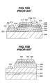
- Fig. 15A is a cross sectional view of a semiconductor light emitting device disclosed in Japanese Patent Laid-open Publication No. 2003-224297.
- a buffer layer 201 is formed on a sapphire substrate 200.
- an n-type contact layer 202 of n-type GaN, an n-type clad layer 203 of n-type AlGaN, a light emitting or luminous layer 204 of InGaN, a p-type clad layer 205 of p-type AlGaN and a p-type contact layer 206 of p-type GaN are stacked in this order.
- the layers from the p-type contact layer 206 to the surface layer of the n-type contact layer 202 are etched to expose a partial area of the n-type contact layer 202.
- a p-side ohmic electrode 207 is formed on the p-type contact layer 206 and an n-side ohmic electrode 208 is formed on the exposed surface of the n-type contact layer 202.
- the lamination structure of these layers is covered with a translucent insulating film 210. Openings 210a and 210b are formed through the insulating film 210 to expose partial surfaces of the n-side ohmic electrode 208 and p-side ohmic electrodes 207, respectively.
- a reflection film 211 is formed on the insulating film 210, covering the p-side ohmic electrode 207.
- a p-side pad 213 is formed on a partial surface of the reflective film 211, and an n-side pad 212 is formed on the n-side ohmic electrode 208.
- the reflection film 211 is made of Al, Ag or Rh and reflects light radiated in the luminous layer 204 toward the substrate 200 side. Light passes through the substrate 200 to be output to an external. In order to improve a light output efficiency, it is desired to increase a reflectance of the reflection film 211.
- Ag has a very high reflectance in the range from ultraviolet light to visual light. Ag is, however, the metal likely to evolve electrochemical migration. According to "High Reliability Micro Soldering Techniques" by Tadashi TAKEMOTO and Ryouhei SATO (Kogyou Chousakai, Publishing, Co., Ltd), the Ag migration evolution mechanism is described as in the following.
- Fig. 15B is a cross sectional view of a semiconductor light emitting device disclosed in Japanese Patent Laid-open Publication No. 2003-168823.
- an AIN buffer layer 221, an n-type GaN layer 222, an InGaN luminous layer 223 and a p-type GaN layer 224 are stacked in this order.
- the p-type GaN layer 224 and luminous layer 223 are partially etched to expose a partial area of the n-type GaN layer 222.
- an Ag layer 225 is formed being covered with a silicon oxide film 227.
- a via hole is formed through the silicon oxide film 227 to expose a partial upper surface of the Ag layer 225.
- An Au layer 228 is formed on the silicon oxide film 227. The Au layer 228 is connected to the Ag layer 225 via the via hole formed through the silicon oxide film 227.
- an n-side ohmic electrode 226 is formed which has a lamination structure of a V layer and an Al layer. Since the Ag layer 225 is covered with the silicon oxide film 227, Ag migration can be suppressed.
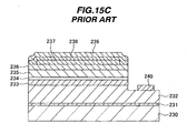
- Fig. 15C is a cross sectional view of a semiconductor light emitting device disclosed in Japanese Patent Laid-open Publication No. HEI-11-220171.
- an AIN buffer layer 231, an n-type GaN layer 232, an n-type GaN clad layer 233, a luminous layer 234, a p-type GaN clad layer 235 and a p-type GaN contact layer 236 are stacked in this order.
- the lamination structure from the p-type GaN contact layer 236 to n-type GaN clad layer 233 is partially etched to expose a partial area of the n-type GaN layer 232.
- An Ag layer 237 is formed on a partial surface of the p-type GaN contact layer 236.
- the Ag layer 237 is covered with a V layer 238 and an Al layer 239 so that Ag migration can be suppressed.
- Ag migration can be suppressed by covering the Ag layer used as the reflection film and electrode with an insulating film or another metal film.
- this migration suppression effect is not sufficient. It is desired to provide a semiconductor light emitting device capable of effectively suppress Ag migration.
- An object of this invention is to provide a semiconductor light emitting device capable of suppressing migration and improving reliability although it uses the metal likely to evolve migration.
- a semiconductor light emitting device comprising: a luminous lamination structure including a first layer made of n-type nitride semiconductor and a second layer made of p-type nitride semiconductor and disposed over the first layer wherein a luminous region is defined between the first and second layers and the second layer is removed to expose the first layer in a first area which is a partial surface of the first layer; a p-side electrode disposed on a surface of the second layer and electrically connected to the second layer; an insulating film covering the p-side electrode; an n-side electrode electrically connected to the first layer in the first area; and a reflection film disposed on the insulating film, extending to the n-side electrode, electrically connected to the n-side electrode, and made of silver containing alloy or silver.
- the reflection film may be made in an electrically floating state.
- the reflection film is connected to the n-side electrode, i.e., cathode. It is therefore possible to suppress ionization of metal constituting the reflection film and suppress the generation of migration.
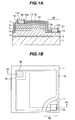
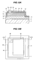
- Fig. 1A is a cross sectional view of a semiconductor light emitting device according to the first embodiment
- Fig. 1 B is a plan view of the device shown in Fig. 1A
- a cross sectional view taken along one-dot chain line A1-A1 shown in Fig. 1B corresponds to Fig. 1A.
- an initial nucleus forming layer 2 an n-type contact layer 3, an n-type clad layer 4, a luminous layer 5, a p-type clad layer 6, a p-type contact layer 7 are stacked in this order.
- a first area 25 of a partial substrate in-plane the layers from the p-type contact layer 7 to a surface layer of the n-type contact layer 3 are etched to partially expose the n-type contact layer 3.
- a p-side ohmic electrode 10 is formed on the p-type contact layer 7.
- the p-side ohmic electrode 10 is made of platinum (Pt) and has a thickness of about 5 nm.
- An n-side ohmic electrode 11 is formed on the surface of the n-type contact layer 3 in the first area 25.
- the n-side ohmic electrode 11 has a two-layer structure of an Al layer having a thickness of about 3 nm and a rhodium (Rh) layer having a thickness of about 100 nm.
- the p-side ohmic electrode 10 and n-side ohmic electrode 11 are in ohmic contact with the p-type contact layer 7 and n-type contact layer 3, respectively.
- An adhesion layer (not shown) made of Ti, Ni, W, Mo or the like and having a thickness of 0.3 nm to 3 nm is formed on the p-side ohmic electrode 10 and n-side ohmic electrode 11.
- the adhesion layer can improve adhesion to an insulating film 15 deposited on the adhesion film.
- the insulating film 15 is formed on the substrate, covering the p-side ohmic electrode 10 and n-side ohmic electrode 11.
- the insulating film 15 is made of silicon oxide and has a thickness of about 300 nm. Openings 15a and 15b are formed through the insulating film 15. A partial surface of the p-side ohmic electrode 10 is exposed on the bottom of the opening 15a, and a partial surface of the n-side ohmic electrode 11 is exposed on the bottom of the opening 15b.
- a reflection film 16 is formed on the insulating film 15.
- the reflection film 16 extends from the area superposed upon the p-side ohmic electrode 10 to the upper surface of the n-side ohmic electrode 11 in the first area 25, and is electrically connected to the n-side ohmic electrode 11 exposed on the bottom of the opening 15b.
- the reflection film 16 is made of silver (Ag) and has a thickness of about 200 nm.
- An adhesion layer (not shown) made of Ti, Ni, Al, W, Mo or the like and having a thickness of 0.3 nm to 3 nm is inserted between the insulating film 15 and reflection film 16. This adhesion layer improves adhesion properties between the insulating film 15 and reflection film 16. A similar adhesion layer (not shown) is formed also on the reflection film 16. This adhesion layer improves adhesion to a protective film 17 to be formed thereon.
- the upper adhesion layer has a thickness of, for example, 10 nm.
- a p-side pad electrode 20 is formed on the p-side ohmic electrode 10 exposed on the bottom of the opening 15a, and an n-side pad electrode 21 is formed on the n-side ohmic electrode 11 exposed on the bottom of the opening 15b.
- the p-side pad electrode 20 and n-side pad electrode 21 have a multi-layer structure of Ti/Pt/Au/(Pt/Au) n where n is the number of repetitions of two layers of a Pt layer and an Au layer.
- a thickness of the lowermost Ti layer is, for example, 3 nm and a thickness of each of the Pt layer and Au layer is, for example, 100 nm.
- the number of repetitions is, for example, 2.
- the number n of repetitions is preferably 1 to 5 from the viewpoint of film forming works and an amount of material to be used. If flip chip bonding is to be performed, it is preferable to set a thickness of the third Au layer of the n-side pad electrode 21 as measured from the substrate side to 100 nm to 1000 nm to make the upper surface height of the n-side pad electrode 21 be flush with the upper surface height of the p-side pad electrode 20.
- An adhesion layer (not shown) made of Ti, Ni, Al, W, Mo or the like and having a thickness of 0.3 nm to 3 nm is formed on the p-side pad electrode 20 and n-side pad electrode 21. This adhesion layer improves adhesion to a protective film 17 to be deposited thereon.
- the protective film 17 is formed covering the reflection film 16 and pad electrodes 20 and 21.
- the protective film 17 is made of silicon oxide and has a thickness of 100 nm to 300 nm, preferably about 200 nm. Openings 17a and 17b are formed through the protective film 17. The upper surfaces of the p-side pad electrode 20 and n-side pad electrode 21 are exposed on the bottoms of the openings 17a and 17b, respectively.
- the plan shape of one semiconductor light emitting device is, for example, a square having one side length of 300 ⁇ m.
- the first area 25 contains one vertex of the square and is constituted of an area near this vertex.
- the shape of the first area is a sector shape having a center angle of 90 ° around one vertex.
- the p-side ohmic electrode 10 is disposed in an area excluding the first area 25 and occupies most of the surface of the semiconductor light emitting device.
- the p-side pad electrode 20 is disposed in an area near the diagonally opposite vertex to the vertex contained in the first area 25.
- the reflection film 16 occupies most of the surface of the semiconductor light emitting device excluding the area where the p-side pad electrode 20 is disposed.
- Each of the layers from the initial nucleus forming layer 2 to the p-type contact layer 7 formed on the underlying substrate 1 made of sapphire is formed, for example, metal organic vapor phase epitaxial (MOVPE) growth, molecular beam epitaxial (MBE) growth or the like.
- MOVPE metal organic vapor phase epitaxial
- MBE molecular beam epitaxial
- etching is performed down to the surface layer region of the n-type contact layer 3 by reactive ion etching to partially expose the n-type contact layer 3. After etching, the resist pattern used as the mask is removed. On the exposed surface of the n-type contact layer 3, the n-side ohmic electrode 11 is formed by electron beam vacuum deposition and lift-off.
- the p-side ohmic electrode 10 and n-side ohmic electrode 11 may be formed after the surface of the n-type contact layer 3 is partially exposed.
- the insulating film 15 is formed by sputtering.
- the openings 15a and 15b are formed through the insulating film 15.
- the openings 15a and 15b may be formed by lift-off.
- the lower adhesion layer, reflection film 16 and upper adhesion layer are formed by electron beam vacuum deposition and lift-off.
- the boundary of the reflection film 16 is retracted from the boundary of the opening 15a by 1 ⁇ m or longer, preferably by about 5 ⁇ m.
- an overlap width of about 3 ⁇ m to 5 ⁇ m is retained between the reflection film 16 and opening 15b. In this manner, the reflection film 16 is not connected to the p-side ohmic electrode 10, but is electrically connected to the n-side ohmic electrode 11.
- the p-side pad electrode 20, n-side pad electrode 21 and adhesion layers thereon are formed by electron beam vacuum deposition and lift-off.
- the p-side pad electrode 20 is preferably formed in such a manner that the outer periphery thereof is disposed slightly inner than the boundary of the opening 15a. If the p-side pad electrode 20 does not contact the reflection film 16, the area near the outer periphery of the p-side pad electrode 20 may overlap the insulating film 15.
- the protective film 17 is formed by sputtering. Thereafter, the openings 17a and 17b are formed through the protective film 17.
- the openings 17a and 17b may be formed by lift-off.
- the surface of the p-side pad electrode 20 is exposed on the bottom of the opening 17a, and the n-side pad electrode 21 is exposed on the bottom of the opening 17b.
- the bottom surface of the underlying substrate 1 is ground and polished to thin the thickness of the underlying substrate 1 ⁇ m to about 100 ⁇ m.
- the thickness of the underlying substrate 1 may be 60 ⁇ m to 210 ⁇ m. Scribing and breaking are performed to separate the wafer into light emitting devices. Each separated light emitting device can be used in various application fields. For example, the separated light emitting device is flip-chip-bonded to a submount substrate.
- the underlying substrate 1 may be adhered to a light guiding plate by transparent adhesive, and the p-side pad electrode 20 and n-side pad electrode 21 are connected to wiring lines formed on the light guiding plate by gold wires.
- the lamination structure constituted of the n-type clad layer 4, luminous layer 5 and p-type clad layer 6, light is radiated in the luminous layer 5.
- Light radiated in the luminous layer 5 passes through the underlying substrate 1 and is irradiated to an external.
- Light radiated in the luminous layer 5 and propagated toward the p-type clad layer 6 passes through the p-side ohmic electrode 10 and insulating film 15, is reflected by the reflection film 16 toward the underlying substrate 1, passes through the underlying substrate 1 and is irradiated to the external.
- Ag migration may be ascribed to that Ag is dissolved at the anode when an electric field is applied under the existence of moisture.
- the reflection film 16 made of Ag is connected to the cathode (n-side ohmic electrode 11), Ag will not be dissolved so that Ag migration can be suppressed.
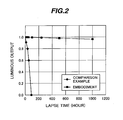
- Fig. 2 shows the result of a lifetime evaluation test of the semiconductor light emitting device of the first embodiment.
- the abscissa represents a lapse time in the unit of "hour" and the ordinate represents a luminous output indicated by a relative scale.
- the result of the lifetime evaluation test of a semiconductor light emitting device is shown, the device having the structure that the p-side ohmic electrode 10 shown in Fig. 1A is made of Ag and used as the reflection film.
- a black rectangle symbol in Fig. 2 shows a change with time of the luminous output of the semiconductor light emitting device of the first embodiment, and a black circle symbol shows a change with time of the luminous output of the semiconductor light emitting device of the comparative example.
- the lifetime evaluation test measured a luminous output in the atmospheric air while the semiconductor light emitting device is flip-chip-bonded to a sub-mount substrate. The luminescence wavelength was 405 nm.
- the luminous output of the semiconductor light emitting device of the comparative example abruptly lowers in several tens hours, whereas the luminous output of the semiconductor light emitting device of the embodiment hardly lowers even after the lapse of 1000 hours.
- the semiconductor light emitting device can have a long lifetime.
- the p-side ohmic electrode 10 is made of Pt, it may be made of a different conductive material which allows light in the luminescence wavelength range of the luminous layer 5 to transmit and can have an ohmic contact with the p-side contact layer 7.
- Such materials may be rhodium (Rh), palladium (Pd) and the like.
- Rh rhodium
- Pd palladium
- a two-layer structure of a Pt layer and an Rh layer or a two-layer structure of an Ni layer and an Au layer may also be adopted. If a two-layer structure of an Ni layer and an Au layer is used, an annealing process is required to be performed after the layers are formed in order to obtain an ohmic contact.
- a translucent oxide film made of oxide of Au and Ni may be used. In this case, after the layer is formed, an annealing process in an oxidizing atmosphere is required to be performed.
- the n-side ohmic electrode 11 has the two-layer structure of an Al layer and an Rh layer (Al/Rh structure)
- a different structure capable of obtaining an ohmic contact with the n-side contact layer 3 may be used.
- usable structures include an Al/Pt structure, an Al/Ir structure, an Al/Pd structure, a Ti/Al structure and a V/Al structure. If the Ti/Al structure or V/Al structure is adopted, an annealing process is necessary after the layers are formed, in order to obtain an ohmic contact.
- the insulating film 15 is made of silicon oxide, it may be made of different insulating material which allows light in the radiation range of the luminous layer 5 to transmit.
- usable materials of the insulating film may be oxide such as titanium oxide (TiO 2 ), tantalum oxide (Ta 2 O 5 ), alumina (Al 2 O 3 ), zirconium oxide (ZrO 2 ) and hafnium oxide (HfO 2 ), heat resistant organic polymeric material such as polyimide, and the like.
- the p-side pad electrode 20 has the multi-layer structure of Ti/Pt/Au/(Pt/Au) n , it may have a different multi-layer structure such as Ti/Rh/Au/(Pt/Au) n and Ni/Rh/Au/(Pt/Au) n .
- a thickness of the lower most layer of the Ti or Ni layer is set to, for example, 0.3 nm to 1 nm.
- a thickness of each of upper Rh, Pt and Au layers is set to 100 nm.
- the number n of repetitions is set to 1 to 5.
- the multi-layer structure satisfying these conditions allows the p-side pad electrode 20 to present the function of the reflection film, and improves the light output efficiency.
- the reflection film 16 is made of Ag, it may be made of alloy which contains Ag as a main composition.
- a thickness of the reflection film 16 is preferably set to 80 nm or thicker in order not to allow light radiated in the luminous layer 5 to transmit. Even if the reflection film 16 is made of the metal other than Ag likely to invoke migration, the migration suppression effect can be expected. This embodiment is particularly effective when the reflection film 16 is made of the metal likely to invoke migration more than the p-side ohmic electrode 10.
- the protective film 17 is made of silicon oxide, it may be made of different insulating material.
- usable materials of the insulating film may be oxide such as titanium oxide (TiO 2 ), tantalum oxide (Ta 2 O 5 ), alumina (Al 2 O 3 ), zirconium oxide (ZrO 2 ) and hafnium oxide (HfO 2 ), heat resistant organic polymeric material such as polyimide, and the like.
- a conductive layer may be formed which is made of metal such as Al having a larger ionization tendency than Ag.
- metal such as Al having a larger ionization tendency than Ag.
- the p-side ohmic electrode 10, insulating film 15 and reflection film 16 constitute the multi-layer reflection film.
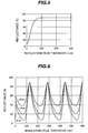
- the reflectance is dependent upon the thicknesses of these films. It is difficult to determine from experiments the conditions suitable for raising the reflectance of the multi-layer film constituted of a metal thin film and a dielectric film. Therefore, the film thickness dependency of a reflectance of a multi-layer reflection film was evaluated by simulation. The evaluation result by simulation will be described hereinunder.
- Fig. 3 shows a model of a multi-layer reflection film used by simulation.
- a contact layer 7 made of GaN On a contact layer 7 made of GaN, a p-side ohmic electrode 10 of Pt, an adhesion layer 10a of Ti, an insulating film 15 of SiO 2 , an adhesion layer 16a of Ti and a reflection film 16 of Ag are stacked in this order.
- a reflectance of light having a wavelength of 460 nm and propagating from the contact layer 7 to the reflection film 16 was obtained by simulation.
- Fig. 4 shows the relation between a thickness of the p-side ohmic electrode 10 and a reflectance.
- the abscissa represents a thickness of the p-side ohmic electrode 10 in the unit of "nm” and the ordinate represents a reflectance in the unit of "%".
- the thicknesses of the adhesion layer 10a, insulating film 15, adhesion layer 16a and reflection film 16 were set to 0.3 nm, 285 nm, 0.3 nm and 200 nm, respectively.
- the reflectance is hardly influenced by the film thickness in the film thickness range equal to or thinner than 7 nm of the p-side ohmic electrode 10. In the film thickness range equal to or thicker than 7 nm, the reflectance lowers as the film thickness increases.
- Fig. 5 shows the relation between a thickness of the reflection film 16 and a reflectance.
- the abscissa represents a thickness of the reflection film 16 in the unit of "nm” and the ordinate represents a reflectance in the unit of "%”.
- the thicknesses of the p-side ohmic electrode 10, adhesion layer 10a, insulating film 15 and adhesion layer 16a were set to 5 nm, 0.3 nm, 285 nm and 0.3 nm, respectively. It can be understood that as the reflection film 16 becomes thick, the reflectance increases and the reflectance saturates at a film thickness of near 80 nm. It can be understood from this result that the thickness of the reflection film 16 is preferably set to 80 nm or thicker.
- Fig. 6 shows the relation between a thickness of the insulating film 15 and a reflectance.
- the abscissa represents a thickness of the insulating film 15 in the unit of "nm” and the ordinate represents a reflectance in the unit of "%".
- the thicknesses of the adhesion layer 10a, adhesion layer 16a and reflection film 16 were set to 0.3 nm, 0.3 nm and 200 nm, respectively.
- Three curves in Fig. 6 show reflectances at the thicknesses of 3 nm, 5 nm and 8 nm of the p-side ohmic electrode 10.
- the reflectance changes periodically in accordance with a change in the thickness of the insulating film 15.
- the reflectance takes maximum values at the thicknesses of the insulating film 15 near about 130 nm, 286 nm and 440 nm.
- the reflectance at the minimum value lowers as the p-side ohmic electrode 10 becomes thicker.
- the p-side ohmic electrode 10 is made thin. If the p-side ohmic electrode is made too thin, it is not possible to achieve the primary object of the electrode that carriers should be injected uniformly into the p-type contact layer 7.
- the thickness of the p-side ohmic electrode 10 is preferably set to 1 nm to 15 nm and more preferably to 3 nm to 8 nm.
- the thickness of the p-side ohmic electrode 10 may be thinned to 1 nm to 5 nm and a mesh type auxiliary electrode of Pt or Rh may be formed on the p-side ohmic electrode.
- a width of one electrode constituting the mesh is set to 2 ⁇ m to 5 ⁇ m, and a distance between electrodes is set to 10 ⁇ m to 15 ⁇ m.
- the measured reflectance of an actually formed evaluation sample had a maximum value at a thickness of near 300 nm of the insulating film 15, although simulation indicates a maximum reflectance at a thickness of about 286 nm of the insulating film 15.
- a shift of the optimum film thickness of the insulating film 15 obtained by experiments from the optimum film thickness of the insulating film 15 obtained by simulation may be ascribed to that the optical characteristics of each film used by simulation do not correctly coincide with the optical characteristics of each film actually formed.
- the thickness of the insulating film 15 is preferably set to 100 nm to 600 nm and more preferably to 200 nm to 400 nm.
- Figs. 7 and 8 show the relation between a thickness of the insulating film 15 and a reflectance, at different wavelengths.
- the abscissa represents a thickness of the insulating film in the unit of "nm” and the ordinate represents a reflectance in the unit of "%”.
- the thicknesses of the p-side ohmic electrode 10, adhesion layer 10a, adhesion layer 16a and reflection film 16 were set to 5 nm, 0.3 nm, 0.3 nm and 200 nm, respectively.
- a numerical number added to each of a plurality of curves shown in Figs. 7 and 8 indicates the wavelength of light to be reflected.
- the thickness of the insulating film 15 at the maximum reflectance changes. It is preferable to set the thickness of the insulating film 15 near to a thickness providing the maximum reflectance, in accordance with the wavelength of light radiated in the luminous layer.
- the film thickness conditions for increasing the reflectance have been obtained through simulation.
- the refractive index and attenuation coefficient of each film change more or less depending upon a film forming method.
- the reflectance is also influenced by a surface roughness of a film. It is therefore preferable to determine an optimum film thickness of each film, by forming a plurality of evaluation samples having different film thicknesses by referring to the optimum film thickness and by measuring actual reflectances.
- the simulation results can be used as the criterion of determining a thickness of each film of the evaluation sample.
- a sapphire substrate having a thickness of 320 ⁇ m was used as the p-side contact layer 7 shown in Fig. 3.
- Pt films having thicknesses of 5 nm, 8 nm and 10 nm were used as the p-side ohmic electrode 10.
- a Ti film having a thickness of 0.3 nm was used as the adhesion layers 10a and 16a.
- An SiO 2 film having a thickness of 313 nm was used as the insulating film 15.
- An Ag film having a thickness of 200 nm was used as the reflection film 16.
- a warp is formed on the substrate. As the warp is formed on the substrate, it is not possible to correctly adjust the incidence angle of incidence light to be used for measuring a reflectance. From this reason, a sapphire substrate not formed with a GaN layer was used as the measurement sample.
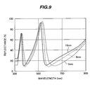
- Fig. 9 shows the measurement results of reflectances.
- the abscissa represents a wavelength in the unit of "nm” and the ordinate represents a reflectance in the unit of "%".
- the samples actually formed had maximum reflectances in the wavelength range of 350 nm to 360 nm and in the wavelength range of 510 nm to 520 nm.
- Fig. 10 is a plan view of a semiconductor light emitting device of the second embodiment.
- the reflection film 16 is made of a plain film and superposes most area of the p-side ohmic electrode 10.
- a reflection pattern 16a of a grid shape is disposed.
- the other fundamental structure is similar to that of the semiconductor light emitting device of the first embodiment.
- a p-side pad electrode 20 and an n-side pad electrode 21 are disposed slightly inside of the central area of a pair of opposing sides of a rectangle, they may be disposed near at the vertexes of the rectangle as in the case of the first embodiment shown in Fig. 1 B.
- light radiated in the luminous layer is irradiated to an external via the support substrate and to the side opposite to the support substrate via openings of the reflection pattern 16a.
- Light is also scattered by the reflection pattern 16a and irradiated to the side of the semiconductor light emitting device.
- Fig. 11 is a schematic cross sectional view of a lamp having the semiconductor light emitting device of the second embodiment built therein.
- the semiconductor light emitting device 28 shown in Fig. 10 is mounted with the support substrate directed to the frame side.
- a cathode lead 31 extends from the frame 30.
- An n-side pad electrode 21 of the semiconductor light emitting device 28 is connected to the frame 30 via a gold wire 35.
- the p-side pad electrode 20 is connected to an anode lead 32 via a gold wire 36.
- the fluorescent member 37 buries the recess of the frame 30.
- the semiconductor light emitting device 28 is covered with the fluorescent member 37.
- the frame 30, cathode lead 31 and anode lead 32 are molded with sealing resin 38.
- the reflection pattern 16a of the grid shape is used, another pattern having openings and scattering light may be used.
- a stripe pattern, a honeycomb pattern or the like may be used.
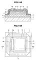
- Fig. 12A is a cross sectional view of the semiconductor light emitting device of the third embodiment
- Fig. 12B is a plan view thereof.
- a cross sectional view taken along one-dot chain line A12-A12 shown in Fig. 12B corresponds to Fig. 12A. Description will be made on different points from the semiconductor light emitting device of the first embodiment.
- the n-side pad electrode 21 is disposed on the n-side ohmic electrode 11, whereas in the second embodiment, an n-side pad electrode 21 is disposed over a p-side ohmic electrode 10 and contacts a reflection film 16.
- a p-side pad electrode 20 and the n-side pad electrode 21 are exposed on the bottoms of openings 17a and 17b formed through a protective film 17.
- the n-side ohmic electrode 11 is disposed along one side of a support substrate 1.
- the p-side pad electrode 20 is disposed near at one end of the side facing the side along which the n-side ohmic electrode 11 is disposed.
- the reflection film 16 occupies most of the area where the p-side pad electrode 20 is not disposed.
- the n-side pad electrode 21 occupies most of the area where the reflection film 16 superposes the p-side ohmic electrode 10.
- Fig. 13 is a schematic cross sectional view of a lamp having the semiconductor light emitting device of the third embodiment built therein.
- the semiconductor light emitting device 50 of the third embodiment is flip-chip-bonded to a sub-mount substrate 43.
- the p-side pad electrode 20 and n-side pad electrode 21 of the semiconductor light emitting device 50 are connected to respective anode wiring 44 and cathode wiring 45 formed on the sub-mount substrate 43.
- the sub-mount substrate 43 is fixed to a stem 40.
- An anode lead 42 and a cathode lead 41 are fixed to the stem 40.
- the anode wiring 44 is connected to the anode lead 42 via a gold wire 46
- the cathode wiring 45 is connected to the cathode lead 41 via a gold wire 47.
- the semiconductor light emitting device 50 and sub-mount substrate 43 are sealed with sealing resin 48. Light radiated in the luminous layer of the semiconductor light emitting device 50 is reflected by the reflection film 16 shown in Fig. 12A and transmits through the support substrate 1 and sealing resin 48 to be irradiated to an external.
- the n-side pad electrode 21 occupies a broader area of the device surface, as compared to the semiconductor light emitting device of the first embodiment. Via this broad n-side pad electrode 21, heat generated in the device efficiently flows to the sub-mount substrate 43. A good heat radiation effect can therefore be retained.
- Fig. 14A is a cross sectional view of the semiconductor light emitting device of the fourth embodiment
- Fig. 14B is a plan view thereof.
- a cross sectional view taken along one-dot chain line A14-A14 shown in Fig. 14B corresponds to Fig. 14A.
- four n-side ohmic electrodes 11 are disposed along four sides of a support substrate 1 of a square shape.
- a reflection film 16 is connected to four n-side ohmic electrodes 11.
- An opening 16a is formed through the reflection film 16 in such a manner that a p-side pad electrode 20 exists in this opening. By forming this opening 16a, a short circuit between the reflection film 16 and p-side pad electrode 20 can be avoided.
- n-side ohmic electrodes 11 since four n-side ohmic electrodes 11 are formed, a contact area of the electrodes can be broadened so that a contact resistance can be lowered. Since four n-side ohmic electrodes 11 are disposed along the four sides of the square, a current deviation in the substrate in-plane can be reduced.
- the areas near the vertexes of the support substrate 1 are likely to be broken during device separation. It is therefore preferable that the n-side ohmic electrodes 11 are not extended near to the vertexes of the support substrate 1.
- the whole side area of a mesa portion constituted of the lamination structure from the n-type clad layer 4 to p-type clad layer 7 is covered with the reflection film 16. It is therefore possible to efficiently reflect light irradiated from the luminous layer 5 toward the side portion, toward the support substrate 1 side and improve the light output efficiency.
- the inclination angle of the side wall of the mesa portion is preferably set to 60 ° or larger.
- a nitride semiconductor layer is dry-etched. Since the resist pattern is also gradually etched, the side wall of the mesa portion of the nitride semiconductor is made inclined in correspondence with the inclination of the side wall of the resist pattern.
- the reflection film 16 may be made in a floating state by connecting it neither to the p-side ohmic electrode 10 nor to the n-side ohmic electrode 11. Also in the floating state, migration can be suppressed more than when the reflection film is connected to the anode as shown in Fig. 15B and 15C.
Abstract

Description
Claims (17)
- A semiconductor light emitting device comprising:a luminous lamination structure including a first layer made of n-type nitride semiconductor and a second layer made of p-type nitride semiconductor and disposed over the first layer wherein a luminous region is defined between the first and second layers and the second layer is removed to expose the first layer in a first area which is a partial surface of the first layer;a p-side electrode disposed on a surface of the second layer and electrically connected to the second layer;an insulating film covering the p-side electrode;an n-side electrode electrically connected to the first layer in the first area; anda reflection film disposed on the insulating film, extending to the n-side electrode, electrically connected to the n-side electrode, and made of silver containing alloy or silver.
- A semiconductor light emitting device according to claim 1, wherein the p-side electrode transmits light having a luminescence wavelength of the luminous region.
- A semiconductor light emitting device according to claim 1, wherein the p-side electrode is made of a metal selected from a group consisting of Pt, Rh and Pd, and has a thickness of 1 nm to 15 nm.
- A semiconductor light emitting device comprising:a luminous lamination structure including a first layer made of n-type nitride semiconductor and a second layer made of p-type nitride semiconductor and disposed over the first layer wherein a luminous region is defined between the first and second layers and the second layer is removed to expose the first layer in a first area which is a partial surface of the first layer;a p-side electrode disposed on a surface of the second layer, electrically connected to the second layer, and transmitting light irradiated from the luminous region;an insulating film covering the p-side electrode;an n-side electrode electrically connected to the first layer in the first area; anda reflection film disposed on the insulating film, extending to the n-side electrode, electrically connected to the n-side electrode, and reflecting light irradiated from the luminous region.
- A semiconductor light emitting device comprising:a luminous lamination structure including a first layer made of n-type nitride semiconductor and a second layer made of p-type nitride semiconductor and disposed over the first layer wherein a luminous region is defined between the first and second layers and the second layer is removed to expose the first layer in a first area which is a partial surface of the first layer;a p-side electrode disposed on a surface of the second layer and electrically connected to the second layer;an insulating film covering the p-side electrode;an n-side electrode electrically connected to the first layer in the first area; anda reflection film disposed on the insulating film, made of silver containing alloy or silver, and made in an electrically floating state, being connected neither to the p-side electrode nor to the n-side electrode.
- A semiconductor light emitting device according to claim 5, wherein the p-side electrode transmits light having a luminescence wavelength of the luminous region.
- A semiconductor light emitting device according to claim 5, wherein the p-side electrode is made of a metal selected from a group consisting of Pt, Rh and Pd, and has a thickness of 1 nm to 15 nm.
- A semiconductor light emitting device comprising:a luminous lamination structure including a first layer made of n-type nitride semiconductor and a second layer made of p-type nitride semiconductor and disposed over the first layer wherein a luminous region is defined between the first and second layers and the second layer is removed to expose the first layer in a first area which is a partial surface of the first layer;a p-side electrode disposed on a surface of the second layer, electrically connected to the second layer, and transmitting light irradiated from the luminous region;an insulating film covering the p-side electrode;an n-side electrode electrically connected to the first layer in the first area; anda reflection film disposed on the insulating film, made in an electrically floating state, being connected neither to the p-side electrode nor to the n-side electrode, and reflecting light irradiated from the luminous region.
- A semiconductor light emitting device according to claim 1, further comprising an intermediate layer disposed between the p-side electrode and the insulating film, the intermediate layer being made of at least a metal selected from a group consisting of Ti, Ni, W and Mo.
- A semiconductor light emitting device according to claim 1, wherein the p-side electrode transmits light having a luminescence wavelength of the luminous region.
- A semiconductor light emitting device according to claim 1, wherein the insulating film is made of at least a material selected from a group consisting of silicon oxide, titanium oxide, tantalum oxide, alumina, zirconium oxide, hafnium oxide, and insulating polymeric material.
- A semiconductor light emitting device according to claim 1, further comprising an insulating protective film covering the reflection film.
- A semiconductor light emitting device according to claim 12, wherein the protective film is made of at least a material selected from a group consisting of silicon oxide, titanium oxide, tantalum oxide, alumina, zirconium oxide, hafnium oxide, and insulating polymeric material.
- A semiconductor light emitting device according to claim 12, further comprising an intermediate layer disposed between the reflection film and the protective film, the intermediate layer being made of at least a metal selected from a group consisting of Ti, Ni, Al, W and Mo.
- A semiconductor light emitting device according to claim 1, further comprising:a p-side pad for flip chip bonding disposed on a partial surface area of the p-side electrode; andan n-side pad for flip chip bonding disposed on a partial surface area of the n-side electrode.
- A semiconductor light emitting device according to claim 1, further comprising:a p-side pad for flip chip bonding disposed on a partial surface area of the p-side electrode; andan n-side pad for flip chip bonding disposed on a surface of the reflection film superposing the second layer.
- A semiconductor light emitting device according to claim 1, wherein the reflection film has a plane shape which scatters light irradiated from the luminous region and propagating toward the reflection film, and the semiconductor light emitting device further comprises a fluorescent material member which produces fluorescence when light scattered by the reflection film becomes incident.
Applications Claiming Priority (2)
| Application Number | Priority Date | Filing Date | Title |
|---|---|---|---|
| JP2004095217A JP4330476B2 (en) | 2004-03-29 | 2004-03-29 | Semiconductor light emitting device |
| JP2004095217 | 2004-03-29 |
Publications (3)
| Publication Number | Publication Date |
|---|---|
| EP1583159A2 true EP1583159A2 (en) | 2005-10-05 |
| EP1583159A3 EP1583159A3 (en) | 2008-11-05 |
| EP1583159B1 EP1583159B1 (en) | 2019-01-30 |
Family
ID=34879909
Family Applications (1)
| Application Number | Title | Priority Date | Filing Date |
|---|---|---|---|
| EP04024366.9A Active EP1583159B1 (en) | 2004-03-29 | 2004-10-13 | Semiconductor light emitting device capable of suppressing silver migration of reflection film made of silver |
Country Status (4)
| Country | Link |
|---|---|
| US (1) | US7141825B2 (en) |
| EP (1) | EP1583159B1 (en) |
| JP (1) | JP4330476B2 (en) |
| TW (1) | TWI262610B (en) |
Cited By (8)
| Publication number | Priority date | Publication date | Assignee | Title |
|---|---|---|---|---|
| WO2007136392A1 (en) | 2006-05-19 | 2007-11-29 | Bridgelux, Inc. | Low optical loss electrode structures for leds |
| WO2009140939A3 (en) * | 2008-05-20 | 2010-01-21 | Osram Opto Semiconductors Gmbh | Optoelectronic semiconductor chip comprising a reflective layer |
| CN102655197A (en) * | 2011-03-01 | 2012-09-05 | 索尼公司 | Light emitting unit and display device |
| EP2403024A3 (en) * | 2010-06-29 | 2014-06-11 | Nichia Corporation | Adhesion layer between electrode and insulating layer for a semiconductor element and corresponding fabrication method |
| TWI473307B (en) * | 2011-10-13 | 2015-02-11 | Automotive Res & Testing Ct | A planar light source light emitting device having a reflective layer |
| CN104576857A (en) * | 2013-10-15 | 2015-04-29 | 上海工程技术大学 | Flip LED chip structure with high reflection layer and manufacturing method of flip LED chip structure |
| EP2325905B1 (en) * | 2009-11-19 | 2017-01-11 | Kabushiki Kaisha Toshiba | Semiconductor light-emitting device and method for manufacturing same |
| EP3751627A3 (en) * | 2009-05-11 | 2021-04-07 | Cree, Inc. | Semiconductor light emitting diodes having reflective structures and methods of fabricating same |
Families Citing this family (105)
| Publication number | Priority date | Publication date | Assignee | Title |
|---|---|---|---|---|
| US10686106B2 (en) | 2003-07-04 | 2020-06-16 | Epistar Corporation | Optoelectronic element |
| US9000461B2 (en) * | 2003-07-04 | 2015-04-07 | Epistar Corporation | Optoelectronic element and manufacturing method thereof |
| US9142740B2 (en) | 2003-07-04 | 2015-09-22 | Epistar Corporation | Optoelectronic element and manufacturing method thereof |
| US20060108672A1 (en) * | 2004-11-24 | 2006-05-25 | Brennan John M | Die bonded device and method for transistor packages |
| DE112005002889B4 (en) * | 2004-12-14 | 2015-07-23 | Seoul Viosys Co., Ltd. | Light emitting device with a plurality of light emitting cells and assembly assembly thereof |
| JP4967243B2 (en) * | 2005-03-08 | 2012-07-04 | 三菱化学株式会社 | GaN-based light emitting diode and light emitting device |
| WO2006095949A1 (en) * | 2005-03-11 | 2006-09-14 | Seoul Semiconductor Co., Ltd. | Led package having an array of light emitting cells coupled in series |
| JP4956902B2 (en) * | 2005-03-18 | 2012-06-20 | 三菱化学株式会社 | GaN-based light emitting diode and light emitting device using the same |
| US7888687B2 (en) * | 2005-09-08 | 2011-02-15 | Showa Denko K.K. | Electrode for semiconductor light emitting device |
| JP4947954B2 (en) * | 2005-10-31 | 2012-06-06 | スタンレー電気株式会社 | Light emitting element |
| JP4777757B2 (en) * | 2005-12-01 | 2011-09-21 | スタンレー電気株式会社 | Semiconductor light emitting device and manufacturing method thereof |
| JP4952884B2 (en) * | 2006-01-24 | 2012-06-13 | ソニー株式会社 | Semiconductor light emitting device and semiconductor light emitting device assembly |
| KR101235460B1 (en) * | 2006-02-14 | 2013-02-20 | 엘지이노텍 주식회사 | Side-View Type Light Emitting Diode and Manufacturing Method thereof |
| JP5153082B2 (en) * | 2006-03-24 | 2013-02-27 | 三洋電機株式会社 | Semiconductor element |
| JP5162909B2 (en) * | 2006-04-03 | 2013-03-13 | 豊田合成株式会社 | Semiconductor light emitting device |
| US7737455B2 (en) * | 2006-05-19 | 2010-06-15 | Bridgelux, Inc. | Electrode structures for LEDs with increased active area |
| US7686469B2 (en) | 2006-09-30 | 2010-03-30 | Ruud Lighting, Inc. | LED lighting fixture |
| US9028087B2 (en) | 2006-09-30 | 2015-05-12 | Cree, Inc. | LED light fixture |
| US9212812B2 (en) | 2013-02-11 | 2015-12-15 | Cree, Inc. | LED light fixture with integrated light shielding |
| US20090086491A1 (en) | 2007-09-28 | 2009-04-02 | Ruud Lighting, Inc. | Aerodynamic LED Floodlight Fixture |
| US9222632B2 (en) | 2013-01-31 | 2015-12-29 | Cree, Inc. | LED lighting fixture |
| US8878245B2 (en) * | 2006-11-30 | 2014-11-04 | Cree, Inc. | Transistors and method for making ohmic contact to transistors |
| US7609004B2 (en) * | 2007-04-05 | 2009-10-27 | World Properties, Inc. | Eliminating silver migration in EL lamps |
| US9484499B2 (en) * | 2007-04-20 | 2016-11-01 | Cree, Inc. | Transparent ohmic contacts on light emitting diodes with carrier substrates |
| US8092042B2 (en) | 2007-05-03 | 2012-01-10 | Ruud Lighting, Inc. | Shield member in LED apparatus |
| JP2008305857A (en) * | 2007-06-05 | 2008-12-18 | Mitsubishi Electric Corp | Optical semiconductor device |
| JP2009059970A (en) * | 2007-08-31 | 2009-03-19 | Seiwa Electric Mfg Co Ltd | Semiconductor light-emitting element and method for fabricating semiconductor light-emitting element |
| US9660153B2 (en) | 2007-11-14 | 2017-05-23 | Cree, Inc. | Gap engineering for flip-chip mounted horizontal LEDs |
| US8575633B2 (en) * | 2008-12-08 | 2013-11-05 | Cree, Inc. | Light emitting diode with improved light extraction |
| US9634191B2 (en) * | 2007-11-14 | 2017-04-25 | Cree, Inc. | Wire bond free wafer level LED |
| US9754926B2 (en) * | 2011-01-31 | 2017-09-05 | Cree, Inc. | Light emitting diode (LED) arrays including direct die attach and related assemblies |
| US8536584B2 (en) * | 2007-11-14 | 2013-09-17 | Cree, Inc. | High voltage wire bond free LEDS |
| US9640737B2 (en) | 2011-01-31 | 2017-05-02 | Cree, Inc. | Horizontal light emitting diodes including phosphor particles |
| US8026527B2 (en) * | 2007-12-06 | 2011-09-27 | Bridgelux, Inc. | LED structure |
| KR101221281B1 (en) * | 2008-03-13 | 2013-01-11 | 쇼와 덴코 가부시키가이샤 | Semiconductor light-emitting device and method for manufacturing the same |
| JP2013038450A (en) * | 2008-03-26 | 2013-02-21 | Panasonic Corp | Semiconductor light-emitting element and light device using the same |
| US7637630B2 (en) * | 2008-04-22 | 2009-12-29 | Ruud Lighting, Inc. | Integrated shield-gasket member in LED apparatus |
| US8384115B2 (en) * | 2008-08-01 | 2013-02-26 | Cree, Inc. | Bond pad design for enhancing light extraction from LED chips |
| TW201021240A (en) * | 2008-11-24 | 2010-06-01 | Harvatek Corp | Wafer level LED package structure for increasing light-emitting efficiency |
| US8741715B2 (en) * | 2009-04-29 | 2014-06-03 | Cree, Inc. | Gate electrodes for millimeter-wave operation and methods of fabrication |
| US7977132B2 (en) * | 2009-05-06 | 2011-07-12 | Koninklijke Philips Electronics N.V. | Extension of contact pads to the die edge via electrical isolation |
| JP5244703B2 (en) | 2009-05-22 | 2013-07-24 | 昭和電工株式会社 | LIGHT EMITTING DIODE, LIGHT EMITTING DIODE LAMP, AND LIGHTING DEVICE |
| US8507935B2 (en) * | 2009-08-06 | 2013-08-13 | Panasonic Corporation | Light emitting element and light emitting device |
| JP5543164B2 (en) * | 2009-09-25 | 2014-07-09 | 豊田合成株式会社 | Light emitting element |
| JP5793292B2 (en) * | 2010-02-17 | 2015-10-14 | 豊田合成株式会社 | Semiconductor light emitting device |
| CN102770975B (en) * | 2010-02-26 | 2015-08-05 | 日亚化学工业株式会社 | Nitride semiconductor luminescent element and manufacture method thereof |
| KR101039948B1 (en) * | 2010-04-23 | 2011-06-09 | 엘지이노텍 주식회사 | Light emitting device, method for fabricating the light emitting device and light emitting device package |
| JP5414627B2 (en) * | 2010-06-07 | 2014-02-12 | 株式会社東芝 | Semiconductor light emitting device and manufacturing method thereof |
| JP2012028381A (en) * | 2010-07-20 | 2012-02-09 | Sharp Corp | Semiconductor light emitting device and method of manufacturing the same |
| JP5633477B2 (en) | 2010-08-27 | 2014-12-03 | 豊田合成株式会社 | Light emitting element |
| US9070851B2 (en) | 2010-09-24 | 2015-06-30 | Seoul Semiconductor Co., Ltd. | Wafer-level light emitting diode package and method of fabricating the same |
| JP5630384B2 (en) * | 2010-09-28 | 2014-11-26 | 豊田合成株式会社 | Group III nitride semiconductor light emitting device manufacturing method |
| US8455882B2 (en) | 2010-10-15 | 2013-06-04 | Cree, Inc. | High efficiency LEDs |
| KR101189081B1 (en) * | 2010-12-16 | 2012-10-10 | 엘지이노텍 주식회사 | Wafer substrate bonding structure, light emitting diode comprising the same and manufacturing method thereof |
| JP2012146926A (en) | 2011-01-14 | 2012-08-02 | Rohm Co Ltd | Light-emitting element, light-emitting element unit and light-emitting element package |
| US9831220B2 (en) | 2011-01-31 | 2017-11-28 | Cree, Inc. | Light emitting diode (LED) arrays including direct die attach and related assemblies |
| US9053958B2 (en) | 2011-01-31 | 2015-06-09 | Cree, Inc. | Light emitting diode (LED) arrays including direct die attach and related assemblies |
| US9673363B2 (en) | 2011-01-31 | 2017-06-06 | Cree, Inc. | Reflective mounting substrates for flip-chip mounted horizontal LEDs |
| US9401103B2 (en) | 2011-02-04 | 2016-07-26 | Cree, Inc. | LED-array light source with aspect ratio greater than 1 |
| US8569889B1 (en) * | 2011-02-09 | 2013-10-29 | Nlight Photonics Corporation | Nano thick Pt metallization layer |
| JP5541260B2 (en) * | 2011-03-21 | 2014-07-09 | 豊田合成株式会社 | Group III nitride semiconductor light emitting device |
| JP5541261B2 (en) * | 2011-03-23 | 2014-07-09 | 豊田合成株式会社 | Group III nitride semiconductor light emitting device |
| JP5652373B2 (en) | 2011-03-24 | 2015-01-14 | 豊田合成株式会社 | Group III nitride semiconductor light emitting device manufacturing method |
| DE102011114865B4 (en) * | 2011-07-29 | 2023-03-02 | OSRAM Opto Semiconductors Gesellschaft mit beschränkter Haftung | Optoelectronic component and method for producing an optoelectronic component |
| JP5321656B2 (en) * | 2011-08-05 | 2013-10-23 | 三菱化学株式会社 | GaN-based light emitting diode and light emitting device |
| JP5304855B2 (en) * | 2011-08-12 | 2013-10-02 | 三菱化学株式会社 | GaN-based light emitting diode and light emitting device using the same |
| KR20130024089A (en) * | 2011-08-30 | 2013-03-08 | 엘지이노텍 주식회사 | Light emitting device |
| TWI479694B (en) * | 2012-01-11 | 2015-04-01 | Formosa Epitaxy Inc | Light emitting diode wafers |
| KR101740531B1 (en) * | 2012-07-02 | 2017-06-08 | 서울바이오시스 주식회사 | Light Emitting Diode Module for Surface Mount Technology and Method of manufacturing the same |
| US9461212B2 (en) | 2012-07-02 | 2016-10-04 | Seoul Viosys Co., Ltd. | Light emitting diode module for surface mount technology and method of manufacturing the same |
| JP5900284B2 (en) * | 2012-10-25 | 2016-04-06 | 豊田合成株式会社 | Semiconductor light emitting element and light emitting device |
| JP5971090B2 (en) * | 2012-11-14 | 2016-08-17 | 豊田合成株式会社 | Semiconductor light emitting element and light emitting device |
| US9435519B2 (en) | 2013-01-31 | 2016-09-06 | Cree, Inc. | Light-fixture support assembly |
| KR102006390B1 (en) | 2013-03-11 | 2019-08-01 | 삼성전자주식회사 | Method of manufacturing Light Emitting diode package |
| DE102013103216A1 (en) * | 2013-03-28 | 2014-10-02 | Osram Opto Semiconductors Gmbh | Radiation emitting semiconductor chip |
| KR102085897B1 (en) * | 2013-06-10 | 2020-03-06 | 엘지이노텍 주식회사 | Light emitting device and light emitting device package |
| DE102013107531A1 (en) | 2013-07-16 | 2015-01-22 | Osram Opto Semiconductors Gmbh | Optoelectronic semiconductor chip |
| JP6215612B2 (en) | 2013-08-07 | 2017-10-18 | ソニーセミコンダクタソリューションズ株式会社 | LIGHT EMITTING ELEMENT, LIGHT EMITTING ELEMENT WAFER, AND ELECTRONIC DEVICE |
| CN106663734B (en) * | 2014-06-10 | 2019-06-14 | 世迈克琉明有限公司 | Semiconductor light-emitting elements |
| FR3023061B1 (en) * | 2014-06-27 | 2017-12-15 | Commissariat Energie Atomique | MESA STRUCTURE DIODE WITH SUBSTANTIALLY PLANE CONTACT SURFACE |
| USD826871S1 (en) | 2014-12-11 | 2018-08-28 | Cree, Inc. | Light emitting diode device |
| JP6827265B2 (en) * | 2015-01-05 | 2021-02-10 | シチズン電子株式会社 | LED light emitting device |
| WO2016157850A1 (en) * | 2015-03-30 | 2016-10-06 | ソニーセミコンダクタソリューションズ株式会社 | Light-emitting element, light-emitting unit, light-emitting panel device, and method for driving light-emitting panel device |
| KR20170003102A (en) * | 2015-06-30 | 2017-01-09 | 엘지이노텍 주식회사 | Light emitting device and light emitting device package comprising the same |
| CN104934514B (en) * | 2015-07-06 | 2018-06-22 | 天津宝坻紫荆科技有限公司 | A kind of composite insulation layer and preparation method |
| KR101744845B1 (en) * | 2015-09-30 | 2017-06-08 | 순천대학교 산학협력단 | Method for manufacturing light emitting diode and light emitting diode using the same |
| CN105226177B (en) * | 2015-10-13 | 2018-03-02 | 厦门市三安光电科技有限公司 | The eutectic electrode structure and flip LED chips of flip LED chips |
| JP6617875B2 (en) * | 2015-12-10 | 2019-12-11 | ウシオ電機株式会社 | LED element and manufacturing method thereof |
| JP7266961B2 (en) | 2015-12-31 | 2023-05-01 | 晶元光電股▲ふん▼有限公司 | light emitting device |
| CN205944139U (en) | 2016-03-30 | 2017-02-08 | 首尔伟傲世有限公司 | Ultraviolet ray light -emitting diode spare and contain this emitting diode module |
| CN105655463B (en) * | 2016-04-11 | 2018-09-18 | 杭州士兰明芯科技有限公司 | A kind of LED structure and preparation method thereof |
| DE102016106831A1 (en) * | 2016-04-13 | 2017-10-19 | Osram Opto Semiconductors Gmbh | Optoelectronic semiconductor chip |
| CN110383509B (en) * | 2016-12-06 | 2022-12-13 | 苏州立琻半导体有限公司 | Light emitting device |
| CN106684223B (en) * | 2016-12-07 | 2019-04-12 | 华灿光电(浙江)有限公司 | A kind of chip of light emitting diode and preparation method thereof |
| KR102237158B1 (en) * | 2017-03-08 | 2021-04-07 | 엘지이노텍 주식회사 | Semiconductor device and semiconductor device package |
| WO2018164371A1 (en) | 2017-03-08 | 2018-09-13 | 엘지이노텍 주식회사 | Semiconductor device and semiconductor device package |
| CN109923683B (en) * | 2017-09-15 | 2022-04-05 | 厦门市三安光电科技有限公司 | Micro light-emitting diode and manufacturing method thereof |
| US20190237629A1 (en) * | 2018-01-26 | 2019-08-01 | Lumileds Llc | Optically transparent adhesion layer to connect noble metals to oxides |
| CN108417682B (en) * | 2018-03-22 | 2020-03-20 | 厦门市三安光电科技有限公司 | Micro light-emitting element and manufacturing method thereof |
| KR102495758B1 (en) * | 2018-08-10 | 2023-02-03 | 삼성전자주식회사 | Flip-chip light emitting diode, manufacturing method of flip-chip light emitting diode and display device including flip-chip light emitting diode |
| KR102300384B1 (en) * | 2019-10-17 | 2021-09-09 | 주식회사 피앤엘세미 | Light emitting diode and manufacturing method therof |
| JP7307662B2 (en) | 2019-10-31 | 2023-07-12 | 日機装株式会社 | Semiconductor light emitting device and method for manufacturing semiconductor light emitting device |
| US11705534B2 (en) | 2020-12-01 | 2023-07-18 | Lumileds Llc | Methods of making flip chip micro light emitting diodes |
| US11955583B2 (en) * | 2020-12-01 | 2024-04-09 | Lumileds Llc | Flip chip micro light emitting diodes |
| WO2024038686A1 (en) * | 2022-08-19 | 2024-02-22 | ソニーセミコンダクタソリューションズ株式会社 | Light-emitting device |
Citations (1)
| Publication number | Priority date | Publication date | Assignee | Title |
|---|---|---|---|---|
| JP2002246647A (en) | 2001-02-16 | 2002-08-30 | Stanley Electric Co Ltd | Wavelength conversion type semiconductor device |
Family Cites Families (16)
| Publication number | Priority date | Publication date | Assignee | Title |
|---|---|---|---|---|
| US5291507A (en) * | 1991-05-15 | 1994-03-01 | Minnesota Mining And Manufacturing Company | Blue-green laser diode |
| US5889295A (en) * | 1996-02-26 | 1999-03-30 | Kabushiki Kaisha Toshiba | Semiconductor device |
| JP3447527B2 (en) * | 1996-09-09 | 2003-09-16 | 株式会社東芝 | Semiconductor light emitting device and method of manufacturing the same |
| JP3503439B2 (en) * | 1997-09-11 | 2004-03-08 | 日亜化学工業株式会社 | Nitride semiconductor device |
| JP3130292B2 (en) * | 1997-10-14 | 2001-01-31 | 松下電子工業株式会社 | Semiconductor light emitting device and method of manufacturing the same |
| US5952681A (en) * | 1997-11-24 | 1999-09-14 | Chen; Hsing | Light emitting diode emitting red, green and blue light |
| JPH11220171A (en) | 1998-02-02 | 1999-08-10 | Toyoda Gosei Co Ltd | Gallium nitride compound semiconductor device |
| US6936859B1 (en) * | 1998-05-13 | 2005-08-30 | Toyoda Gosei Co., Ltd. | Light-emitting semiconductor device using group III nitride compound |
| JP3531475B2 (en) * | 1998-05-22 | 2004-05-31 | 日亜化学工業株式会社 | Flip chip type optical semiconductor device |
| JP2001339101A (en) * | 2000-05-26 | 2001-12-07 | Sharp Corp | Gallium nitride compound semiconductor element |
| US6998281B2 (en) * | 2000-10-12 | 2006-02-14 | General Electric Company | Solid state lighting device with reduced form factor including LED with directional emission and package with microoptics |
| CN1217425C (en) * | 2001-07-12 | 2005-08-31 | 日亚化学工业株式会社 | Semiconductor device |
| JP2003168823A (en) | 2001-09-18 | 2003-06-13 | Toyoda Gosei Co Ltd | Iii nitride based compound semiconductor light emitting element |
| JP4122785B2 (en) | 2002-01-30 | 2008-07-23 | 日亜化学工業株式会社 | Light emitting element |
| JP4123830B2 (en) * | 2002-05-28 | 2008-07-23 | 松下電工株式会社 | LED chip |
| US7239080B2 (en) * | 2004-03-11 | 2007-07-03 | Avago Technologies Ecbu Ip (Singapore) Pte. Ltd | LED display with overlay |
-
2004
- 2004-03-29 JP JP2004095217A patent/JP4330476B2/en not_active Expired - Fee Related
- 2004-10-13 EP EP04024366.9A patent/EP1583159B1/en active Active
- 2004-10-19 US US10/968,761 patent/US7141825B2/en active Active
-
2005
- 2005-03-10 TW TW094107302A patent/TWI262610B/en not_active IP Right Cessation
Patent Citations (1)
| Publication number | Priority date | Publication date | Assignee | Title |
|---|---|---|---|---|
| JP2002246647A (en) | 2001-02-16 | 2002-08-30 | Stanley Electric Co Ltd | Wavelength conversion type semiconductor device |
Cited By (20)
| Publication number | Priority date | Publication date | Assignee | Title |
|---|---|---|---|---|
| US9099613B2 (en) | 2006-05-19 | 2015-08-04 | Bridgelux, Inc. | LEDs with efficient electrode structures |
| EP2018671A1 (en) * | 2006-05-19 | 2009-01-28 | Bridgelux, Inc. | Low optical loss electrode structures for leds |
| US10741726B2 (en) | 2006-05-19 | 2020-08-11 | Bridgelux Inc. | LEDs with efficient electrode structures |
| US10199543B2 (en) | 2006-05-19 | 2019-02-05 | Bridgelux, Inc. | LEDs with efficient electrode structures |
| EP2018671A4 (en) * | 2006-05-19 | 2013-11-20 | Bridgelux Inc | Low optical loss electrode structures for leds |
| WO2007136392A1 (en) | 2006-05-19 | 2007-11-29 | Bridgelux, Inc. | Low optical loss electrode structures for leds |
| US9627589B2 (en) | 2006-05-19 | 2017-04-18 | Bridgelux, Inc. | LEDs with efficient electrode structures |
| US9356194B2 (en) | 2006-05-19 | 2016-05-31 | Bridgelux, Inc. | LEDs with efficient electrode structures |
| US9105815B2 (en) | 2006-05-19 | 2015-08-11 | Bridgelux, Inc. | LEDs with efficient electrode structures |
| US8710512B2 (en) | 2008-05-20 | 2014-04-29 | Osram Opto Semiconductors Gmbh | Optoelectronic semiconductor chip comprising a reflective layer |
| WO2009140939A3 (en) * | 2008-05-20 | 2010-01-21 | Osram Opto Semiconductors Gmbh | Optoelectronic semiconductor chip comprising a reflective layer |
| EP3751627A3 (en) * | 2009-05-11 | 2021-04-07 | Cree, Inc. | Semiconductor light emitting diodes having reflective structures and methods of fabricating same |
| EP2325905B1 (en) * | 2009-11-19 | 2017-01-11 | Kabushiki Kaisha Toshiba | Semiconductor light-emitting device and method for manufacturing same |
| EP2403024A3 (en) * | 2010-06-29 | 2014-06-11 | Nichia Corporation | Adhesion layer between electrode and insulating layer for a semiconductor element and corresponding fabrication method |
| CN102655197B (en) * | 2011-03-01 | 2016-12-14 | 索尼公司 | Luminescence unit and display device |
| CN102655197A (en) * | 2011-03-01 | 2012-09-05 | 索尼公司 | Light emitting unit and display device |
| EP3564997A1 (en) * | 2011-03-01 | 2019-11-06 | Sony Corporation | Light emitting unit and display device |
| TWI473307B (en) * | 2011-10-13 | 2015-02-11 | Automotive Res & Testing Ct | A planar light source light emitting device having a reflective layer |
| CN104576857A (en) * | 2013-10-15 | 2015-04-29 | 上海工程技术大学 | Flip LED chip structure with high reflection layer and manufacturing method of flip LED chip structure |
| CN104576857B (en) * | 2013-10-15 | 2017-07-04 | 上海工程技术大学 | A kind of high reflection layer flip LED chips structure and preparation method thereof |
Also Published As
| Publication number | Publication date |
|---|---|
| JP2005302747A (en) | 2005-10-27 |
| US7141825B2 (en) | 2006-11-28 |
| TWI262610B (en) | 2006-09-21 |
| US20050211989A1 (en) | 2005-09-29 |
| EP1583159B1 (en) | 2019-01-30 |
| TW200535960A (en) | 2005-11-01 |
| EP1583159A3 (en) | 2008-11-05 |
| JP4330476B2 (en) | 2009-09-16 |
Similar Documents
| Publication | Publication Date | Title |
|---|---|---|
| US7141825B2 (en) | Semiconductor light emitting device capable of suppressing silver migration of reflection film made of silver | |
| JP5021693B2 (en) | Semiconductor light emitting device | |
| US8698178B2 (en) | Optoelectronic semiconductor component and method for producing an inorganic optoelectronic semiconductor component | |
| KR100876737B1 (en) | Semiconductor light emitting device and manufacturing method thereof | |
| JP4976849B2 (en) | Semiconductor light emitting device | |
| US8716728B2 (en) | Nitride semiconductor light-emitting diode device | |
| US8643046B2 (en) | Semiconductor light-emitting element, method for producing the same, lamp, lighting device, electronic equipment, mechanical device and electrode | |
| KR101368720B1 (en) | Semiconductor light emimitting device | |
| US9018656B2 (en) | Light emitting device | |
| US20100117109A1 (en) | Light emitting element | |
| US20150357525A1 (en) | Semiconductor device and method for manufacturing same | |
| JP2006253298A (en) | Semiconductor light emitting element and device therefor | |
| KR100955007B1 (en) | Gallium nitride-based compound semiconductor light-emitting device | |
| KR20070038864A (en) | Semiconductor light emitting device | |
| KR20110053064A (en) | Light emitting diode chip and light emitting diode package each having distributed bragg reflector | |
| US20100289047A1 (en) | Light Emitting Element and Illumination Device | |
| JP2010272592A (en) | Semiconductor light emitting element | |
| JP2005302803A (en) | Nitride semiconductor light emitting element and its manufacturing method | |
| KR101378948B1 (en) | Semiconductor light emimitting device | |
| CN210040239U (en) | Light emitting diode | |
| KR101403641B1 (en) | Semiconductor light emimitting device | |
| JPH10341038A (en) | Semiconductor light emitting element | |
| KR101378950B1 (en) | Semiconductor light emimitting device | |
| CN211350691U (en) | Semiconductor light-emitting element | |
| KR102338178B1 (en) | Semiconductor light emitting device |
Legal Events
| Date | Code | Title | Description |
|---|---|---|---|
| PUAI | Public reference made under article 153(3) epc to a published international application that has entered the european phase |
Free format text: ORIGINAL CODE: 0009012 |
|
| AK | Designated contracting states |
Kind code of ref document: A2 Designated state(s): AT BE BG CH CY CZ DE DK EE ES FI FR GB GR HU IE IT LI LU MC NL PL PT RO SE SI SK TR |
|
| AX | Request for extension of the european patent |
Extension state: AL HR LT LV MK |
|
| PUAL | Search report despatched |
Free format text: ORIGINAL CODE: 0009013 |
|
| AK | Designated contracting states |
Kind code of ref document: A3 Designated state(s): AT BE BG CH CY CZ DE DK EE ES FI FR GB GR HU IE IT LI LU MC NL PL PT RO SE SI SK TR |
|
| AX | Request for extension of the european patent |
Extension state: AL HR LT LV MK |
|
| 17P | Request for examination filed |
Effective date: 20090216 |
|
| 17Q | First examination report despatched |
Effective date: 20090327 |
|
| AKX | Designation fees paid |
Designated state(s): DE FR GB |
|
| REG | Reference to a national code |
Ref country code: DE Ref legal event code: R079 Ref document number: 602004053676 Country of ref document: DE Free format text: PREVIOUS MAIN CLASS: H01L0033000000 Ipc: H01L0033320000 |
|
| GRAP | Despatch of communication of intention to grant a patent |
Free format text: ORIGINAL CODE: EPIDOSNIGR1 |
|
| RIC1 | Information provided on ipc code assigned before grant |
Ipc: H01L 33/46 20100101ALI20180726BHEP Ipc: H01L 33/32 20100101AFI20180726BHEP Ipc: H01L 33/44 20100101ALI20180726BHEP Ipc: H01L 33/40 20100101ALI20180726BHEP |
|
| INTG | Intention to grant announced |
Effective date: 20180830 |
|
| GRAS | Grant fee paid |
Free format text: ORIGINAL CODE: EPIDOSNIGR3 |
|
| GRAA | (expected) grant |
Free format text: ORIGINAL CODE: 0009210 |
|
| AK | Designated contracting states |
Kind code of ref document: B1 Designated state(s): DE FR GB |
|
| REG | Reference to a national code |
Ref country code: GB Ref legal event code: FG4D |
|
| REG | Reference to a national code |
Ref country code: DE Ref legal event code: R096 Ref document number: 602004053676 Country of ref document: DE |
|
| REG | Reference to a national code |
Ref country code: DE Ref legal event code: R097 Ref document number: 602004053676 Country of ref document: DE |
|
| PLBE | No opposition filed within time limit |
Free format text: ORIGINAL CODE: 0009261 |
|
| STAA | Information on the status of an ep patent application or granted ep patent |
Free format text: STATUS: NO OPPOSITION FILED WITHIN TIME LIMIT |
|
| 26N | No opposition filed |
Effective date: 20191031 |
|
| PGFP | Annual fee paid to national office [announced via postgrant information from national office to epo] |
Ref country code: GB Payment date: 20230831 Year of fee payment: 20 |
|
| PGFP | Annual fee paid to national office [announced via postgrant information from national office to epo] |
Ref country code: FR Payment date: 20230911 Year of fee payment: 20 |
|
| PGFP | Annual fee paid to national office [announced via postgrant information from national office to epo] |
Ref country code: DE Payment date: 20230830 Year of fee payment: 20 |