TECHNICAL FIELD
The present invention relates to an image correction method and device
that process image signals according to movement of images.
BACKGROUND ART
Conventionally, some suggestions have been made on image signal
correction devices. Such a device detects movement of image and processes
image signal differently between the area with still picture and the area with
motion picture. For example, Japanese Patent Unexamined Publication No.
2001-34229 discloses a method of correcting dynamic pseudo contour. Fig. 8 is
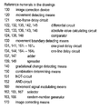
a block diagram of image correction device 20 for correcting dynamic false
contour, which is introduced in the aforementioned disclosure. In Fig. 8, image
correcting means 170 contains adder 3; still-picture coding circuit 4;
motion-picture coding circuit 5; selector 7; differential circuit 11; coefficient
circuit group 12; and delay circuit group 13. With the structure, image
correcting means 170 provides an image signal with error diffusion. Image
correcting means 170 is controlled by the output of movement detecting means
120 such that an error diffusion using the output from still-picture coding
circuit 4 takes place in a still-picture area, while, in a motion-picture area, an
error diffusion using the output from motion-picture coding circuit 5 takes
place.
In such a correction device, however, upon switching of correction process
of image signals according to movement of images, some images have often
produced noise with sharp edge (hereinafter referred to as switch shock) at the
boundary between the still-picture area and the motion-picture area. To
address the problem above, Japanese Patent Unexamined Publication No.
2001-34229 also introduces another image correction device that performs the
diffusion process with the use of random numbers so as not to give sharp lines
to the boundary area, whereby the switch shock is eased. The conventional
image correction device, however, simply provides the boundary area with error
diffusion. Therefore, in some images, the switch shock persists due to an
insufficient diffusion, or another noise like jitters, which is a side effect of the
diffusion, appears along the outlines the image. Avoiding the inconveniencies
above has been an obstacle to an intended correction of dynamic pseudo
contour.
The present invention addresses the problems above. It is therefore the
object of the invention to provide a method and device for image correction
capable of not only performing image signal process according to the movement
of images, but also suppressing the switch shock.
DISCLOSURE OF THE INVENTION
The image correction method of the present invention provides image
signals with image correction selected from a plurality of correction methods
according to the image signal. The method provides the image correction by
following procedures: detecting a motion picture area according to an image
signal; comparing gradation of image signals corresponding to adjoining pixels;
and providing the boundary area of the motion-picture area with diffusion in an
area having gradational change smaller than a predetermined threshold. In
this way, the image correction device switches the correction process between
the boundary-diffused motion-picture area and other areas.
BRIEF DESCRIPTION OF THE DRAWINGS
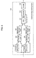
Fig. 1 is a circuit block diagram illustrating the structure of an image
correction device of an exemplary embodiment of the present invention.
Fig. 2 is a circuit block diagram of the movement detecting means of the
image correction device.
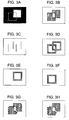
Fig. 3 illustrates the workings of the image correction device.
Fig. 4 is a circuit block diagram of the movement boundary detecting
means of the image correction device.
Fig. 5 is a circuit block diagram of the gradational change detecting
means of the image correction device.
Fig. 6 is a circuit block diagram of the movement signal modulating
means of the image correction device.
Fig. 7 is a circuit block diagram embodying the image correcting means of
the image correction device.
Fig. 8 is a circuit block diagram illustrating the structure of a
conventional image correction device.
DETAILED DESCRIPTION OF CARRYING OUT OF THE INVENTION
An exemplary embodiment of the present invention is described
hereinafter with reference to the accompanying drawings.
EXEMPLARY EMBODIMENT
Fig. 1 is a circuit block diagram illustrating the structure of image
correction device 100 of the exemplary embodiment of the present invention.
As a typical image correction, the description of the embodiment will be made
on correcting dynamic pseudo contour. Receiving an input image signal,
movement detecting means 120 compares the signal to one-frame-before image
signal and detects an area with big temporal gradational change (hereinafter
referred to as a movement area). Movement boundary detecting means 130
detects the boundary area of the movement area. On the other hand, receiving
the input image signal, gradational change detecting means 140 compares the
gradation of adjoining pixels and detects an image area with big spatial
gradational change. Combination determining means 150 determines the area
excluding the image area with big gradational change by the following
procedure: NOT-circuit 151 calculates logical NOT of the output from
gradational change detecting means 140; AND-circuit 152 receives the result
from NOT-circuit 151 and calculates logical conjunction of the result and the
boundary area of the movement area. The logical NOT of the output from
gradational change detecting means 140 shows the image area with small
spatial gradational change (hereinafter, flat area); therefore, the output of
combination determining means 150 shows the boundary area of the movement
area that belongs to the flat area. Movement signal modulating means 160
modulates the output of movement detecting means 120 (as will be described
later), whereas, for other areas, movement signal modulating means 160 sends
the output of movement detecting means 120 to image correcting means 170.
Image correcting means 170 of the embodiment changes a correction method
according to the output of movement signal modulating means 160 so as to
properly correct the dynamic pseudo contour.
Fig. 2 is a circuit block diagram of movement detecting means 120 of the
image correction device of the embodiment. One-frame delay circuit 121
delays an incoming image signal by one frame. Differential circuit 122
calculates the difference between the image signal and the one-frame-delayed
image signal. Absolute value calculating circuit 123 calculates the absolute
value of the difference. Comparator 124 compares the output from absolute
value calculating circuit 123 to a threshold used for determining movement
areas. If the output from absolute value calculating circuit 123 is greater than
the threshold, comparator 124 outputs 1; otherwise, outputs 0. Fig. 3
illustrates the workings of the image correction device of the present invention.
Suppose that an image signal-corresponding to a bright rectangular pattern
moving in the upper-right direction against a dark background, as is shown in
Fig. 3A (where, the rectangular shown by dot lines indicates the
one-frame-before position of the pattern)-is coming in. Receiving the image
signal, comparator 124 outputs movement area signals, as shown in Fig. 3B,
according to the image signal: 1 for the movement area, 0 for other areas.
Fig. 4 is a circuit block diagram of movement boundary detecting means
130 of the image correction device of the embodiment. One-pixel delay circuit
131 delays an incoming movement area signal by one pixel. Differential circuit
132 calculates the difference between the original movement area signal and
the one-pixel-delayed movement area signal. Absolute value calculating
circuit 133 calculates the absolute value of the difference. That is, absolute
value calculating circuit 133 outputs a signal representing the horizontal
boundaries of the movement area, as shown in Fig. 3C. On the other hand,
one-line delay circuit 134 delays the movement area signal by one line.
Differential circuit 135 calculates the difference between the original movement
area signal and the one-line-delayed movement area signal. Absolute value
calculating circuit 136 calculates the absolute value of the difference. That is,
absolute value calculating circuit 136 outputs a signal representing the vertical
boundaries of the movement area. Adder 137 adds the outputs from absolute
value calculating circuits 133 and 136. Comparator 138 compares the outputs
from adder 137 to a threshold used for determining boundaries. If the output
from adder 137 is greater than the threshold, comparator 138 outputs 1;
otherwise, outputs 0. When receiving output of 1 from comparator 138,
spreader 139 gives 1 to adjacent pixels, thereby increasing the area having 1.
In the embodiment, according to the number of delay circuits of movement
signal modulating means 160 (as will be described later), the area having 1 is
extended horizontally by five pixels, and vertically by three pixels.
Comparator 138 outputs 1 with respect to the horizontal 5 pixels and vertical 3
pixels around the boundary of the movement area, and outputs 0 with respect
to other areas, so that the boundary area is extended, as shown in Fig. 3D.
Fig. 5 is a circuit block diagram of gradational change detecting means
140 of the embodiment. Gradational change detecting means 140 contains
one-pixel delay circuit 141; differential circuit 142; absolute value calculating
circuit 143; one-line delay circuit 144; differential circuit 145; absolute value
calculating circuit 146; adder 147; comparator 148; and spreader 149. The
structure above is exactly alike to that of movement boundary detecting means
130, except that gradational change detecting means 140 receives an image
signal as input signal. Comparator 148 outputs a gradational change signal
showing the area with big gradational change, i.e., the boundary of the
rectangular pattern of Fig. 3A. Therefore, as shown in Fig. 3E, comparator
148 outputs 1 with respect to the boundary of the rectangular pattern, and
outputs 0 with respect to other areas. Like spreader 139, spreader 149 gives 1
to horizontal 5 pixels and vertical 3 pixels, thereby increasing the area having 1.
Combination determining means 150 contains, as shown in Fig. 1, NOT-circuit
151 and AND-circuit 152. NOT-circuit 151 calculates logical NOT of a
boundary change signal. Receiving the result from NOT-circuit 151,
AND-circuit 152 calculates logical conjunction of the result and a movement
boundary signal. As a result, the modulation control signal fed from
combination determining means 150, as shown in Fig. 3F, gives 1 with respect
to the boundary area of the movement area belongs to the flat area, and gives 0
with respect to other areas.
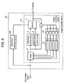
Fig. 6 is a circuit block diagram of movement signal modulating means
160 of the image correction device. Movement signal modulating means 160
modulates a movement area signal so as to provide a movement area with
parallel movement in the horizontal and vertical directions. Movement signal
modulating means 160 contains four one-pixel delay circuits 1611 - 1614, which
sequentially delay a movement area signal by one pixel. According to the
output from random-number generator 163, selector 162 selects one signal from
the original movement area signal and four delayed movement area signals.
Random-number generator 163 generates a random number for each pixel; and
accordingly, selector 162 outputs at latest 4-pixel-delayed movement area signal.
As a result, a random diffusion is applied to the boundary of a movement area
in a horizontal direction, as shown in Fig. 3G. The output from selector 162 is
now fed into selector 165 and one line-delayed circuits 1641, 1642. Selector 165
selects, according to the output from random number-generator 166, one signal,
which provides the boundary of the movement area with a random diffusion in
a vertical direction. When a modulation control signal takes 1, selector 167
selects the horizontally and vertically modulated movement area signal; on the
other hand, when the modulation control signal takes 0, selector 167 selects a
movement area signal with no modulation. The selected signal is fed into
image correcting means 170. As a result, the output from movement signal
modulating means 160 provides the boundary of a movement area with a
selective diffusion. The output signal is fed into image correcting means 170
as a correction control signal.
By virtue of the aforementioned delay circuit, the movement signal
modulating means can be formed of a relatively simple structure. In addition,
using the randomly selected amount of a delay of the delay circuits enables to
provide the movement area with a diffusion having no periodical component,
thereby further suppressing the switch shock. The amount of a delay may be
periodically changed by pixel, line, or field, as long as the switch shock is not
recognized as an eyesore.
Fig. 7 is a circuit block diagram embodying image correcting means 170
of the image correction device of Fig. 1. Image correcting means 170 functions
as a means for correcting dynamic pseudo contour and the structure thereof is
the same as that of image correcting means 170 of the conventional device
shown in Fig. 8. Therefore, the circuit blocks identical to those of image
correcting means 170 bear similar reference numbers and detailed explanation
thereof will be omitted. In Fig. 7, when selector 7 selects the output from
still-picture coding circuit 4, the correction device provides image correction
capable of showing a smooth gradation although dynamic pseudo contour easily
appears; on the other hand, when selector 7 selects the output from
motion-picture coding circuit 5, the correction device provides image correction
for suppressing the dynamic pseudo contour although the number of the
gradation levels decreases.
Now suppose that, like a conventional image correction device, selector 7
selects image correction according to the movement area signal shown in Fig.
3B. In this case, Fig. 3D shows the boundary at which correction control is
switched. The area shown in Fig. 3F of the entire boundary of Fig. 3D is the
boundary between the rectangular pattern and the background in the
one-frame-before image, but in the current frame, it belongs to a flat area with
small gradational change. That is, as described earlier, the boundary area is
supposed to suffer the switch shock. However, according to the embodiment,
the correction control signal shown in Fig. 3H is used for operating selector 7,
and correction control suitable for each area is selected. At the boundary of the
rectangular patterns, the correction control is switched at the boundary,
whereas in the flat area susceptible to the switch shock, the boundary of
correction undergoes selective diffusion. As a result, the switch shock is
preferably suppressed and sufficient correction of dynamic pseudo contour is
performed.
The image correction method of the embodiment, as described above,
differs from the method that simply switches the image correction at the
boundary of the movement area, and also differs from the method that provides
the boundary area with a uniform diffusion. When switching image correction
according to the movement of images, the method of the present invention
provides the boundary area in a flat area-where the switch shock is likely to
occur-with selective diffusion. In this way, the correction method of the
embodiment not only can properly perform the image signal process according
to the movement of images, but also suppresses the switch shock.
Although movement signal modulating means 160 of the embodiment
employs, as shown in Fig. 6, four one-pixel-delay circuits and two one-line-delay
circuits, it is not limited thereto; the number of each delay circuit can be
arbitrarily defined.
In the description above, spreaders 139 and 149 are disposed in the
output-side of comparators 138 and 148, respectively. Receiving the output
signal from comparator 138, spreader 139 extends the width of the boundary
area corresponding to the signal in a horizontal direction; similarly, spreader
149 extends the width of the boundary area corresponding to the signal from
comparator 148 in a vertical direction. However, it is not limited to the
structure above as long as the width of the boundary area can be extended.
For example, disposing a low pass filter in the input-side of a comparator can
provide the same effect.
Although image correcting means 170 of the embodiment is used for
correcting dynamic pseudo contour in the description, it is not limited thereto.
For example, interlace-progressive (IP) converting means, which switches
image interpolation between movement areas and other areas, can generate a
switch shock on a boundary. The image correction device of the embodiment is
applicable to other image corrections as long as the device contains an image
correcting means capable of changing the correction process according to a
control signal that corresponds to movement of images.
The present invention can thus provide a method and device for image
correction in which image signal processes are performed according to the
movement of images, with occurrence of the switch shock preferably
suppressed.
INDUSTRIAL APPLICABILITY
According to the present invention, the image signal process is performed
according to the movement of images, with occurrence of the switch shock
preferably suppressed. The device of the invention is therefore useful as the
method and device for image correction that perform the image signal process
according to movement of images.