EP1608032A2 - Organic electro-luminescence display device and fabricating method thereof - Google Patents
Organic electro-luminescence display device and fabricating method thereof Download PDFInfo
- Publication number
- EP1608032A2 EP1608032A2 EP05012738A EP05012738A EP1608032A2 EP 1608032 A2 EP1608032 A2 EP 1608032A2 EP 05012738 A EP05012738 A EP 05012738A EP 05012738 A EP05012738 A EP 05012738A EP 1608032 A2 EP1608032 A2 EP 1608032A2
- Authority
- EP
- European Patent Office
- Prior art keywords
- organic electro
- seal line
- display device
- line area
- insulating pattern
- Prior art date
- Legal status (The legal status is an assumption and is not a legal conclusion. Google has not performed a legal analysis and makes no representation as to the accuracy of the status listed.)
- Granted
Links
- 238000005401 electroluminescence Methods 0.000 title claims abstract description 59
- 238000000034 method Methods 0.000 title claims abstract description 18
- 239000000758 substrate Substances 0.000 claims abstract description 29
- 239000000565 sealant Substances 0.000 claims abstract description 23
- 238000004519 manufacturing process Methods 0.000 claims description 5
- 239000000463 material Substances 0.000 claims description 5
- 230000008569 process Effects 0.000 abstract description 10
- 230000003044 adaptive effect Effects 0.000 abstract description 3
- 238000005538 encapsulation Methods 0.000 abstract description 3
- 230000004888 barrier function Effects 0.000 description 9
- 238000002347 injection Methods 0.000 description 6
- 239000007924 injection Substances 0.000 description 6
- 108091006149 Electron carriers Proteins 0.000 description 4
- 238000000151 deposition Methods 0.000 description 4
- 239000007769 metal material Substances 0.000 description 4
- ZOKXTWBITQBERF-UHFFFAOYSA-N Molybdenum Chemical compound [Mo] ZOKXTWBITQBERF-UHFFFAOYSA-N 0.000 description 3
- 230000008901 benefit Effects 0.000 description 3
- 238000005530 etching Methods 0.000 description 3
- 229910052751 metal Inorganic materials 0.000 description 3
- 239000002184 metal Substances 0.000 description 3
- 229910052750 molybdenum Inorganic materials 0.000 description 3
- 239000011733 molybdenum Substances 0.000 description 3
- 238000004806 packaging method and process Methods 0.000 description 3
- 238000000206 photolithography Methods 0.000 description 3
- QVGXLLKOCUKJST-UHFFFAOYSA-N atomic oxygen Chemical compound [O] QVGXLLKOCUKJST-UHFFFAOYSA-N 0.000 description 2
- 230000015572 biosynthetic process Effects 0.000 description 2
- 239000007772 electrode material Substances 0.000 description 2
- 239000011810 insulating material Substances 0.000 description 2
- 150000002894 organic compounds Chemical class 0.000 description 2
- 229910052760 oxygen Inorganic materials 0.000 description 2
- 239000001301 oxygen Substances 0.000 description 2
- 238000000926 separation method Methods 0.000 description 2
- XOLBLPGZBRYERU-UHFFFAOYSA-N tin dioxide Chemical compound O=[Sn]=O XOLBLPGZBRYERU-UHFFFAOYSA-N 0.000 description 2
- 239000000853 adhesive Substances 0.000 description 1
- 230000001070 adhesive effect Effects 0.000 description 1
- 230000008021 deposition Effects 0.000 description 1
- 238000010586 diagram Methods 0.000 description 1
- 239000011521 glass Substances 0.000 description 1
- 230000005283 ground state Effects 0.000 description 1
- AMGQUBHHOARCQH-UHFFFAOYSA-N indium;oxotin Chemical compound [In].[Sn]=O AMGQUBHHOARCQH-UHFFFAOYSA-N 0.000 description 1
- 239000004973 liquid crystal related substance Substances 0.000 description 1
- 230000004048 modification Effects 0.000 description 1
- 238000012986 modification Methods 0.000 description 1
- 230000003287 optical effect Effects 0.000 description 1
- 239000011368 organic material Substances 0.000 description 1
- 238000005192 partition Methods 0.000 description 1
- 238000000059 patterning Methods 0.000 description 1
- 230000004044 response Effects 0.000 description 1
- 239000004065 semiconductor Substances 0.000 description 1
- HUAUNKAZQWMVFY-UHFFFAOYSA-M sodium;oxocalcium;hydroxide Chemical compound [OH-].[Na+].[Ca]=O HUAUNKAZQWMVFY-UHFFFAOYSA-M 0.000 description 1
- 238000004528 spin coating Methods 0.000 description 1
- 238000001771 vacuum deposition Methods 0.000 description 1
Images


Classifications
-
- H—ELECTRICITY
- H10—SEMICONDUCTOR DEVICES; ELECTRIC SOLID-STATE DEVICES NOT OTHERWISE PROVIDED FOR
- H10K—ORGANIC ELECTRIC SOLID-STATE DEVICES
- H10K50/00—Organic light-emitting devices
- H10K50/80—Constructional details
- H10K50/84—Passivation; Containers; Encapsulations
- H10K50/842—Containers
- H10K50/8426—Peripheral sealing arrangements, e.g. adhesives, sealants
-
- H—ELECTRICITY
- H10—SEMICONDUCTOR DEVICES; ELECTRIC SOLID-STATE DEVICES NOT OTHERWISE PROVIDED FOR
- H10K—ORGANIC ELECTRIC SOLID-STATE DEVICES
- H10K59/00—Integrated devices, or assemblies of multiple devices, comprising at least one organic light-emitting element covered by group H10K50/00
- H10K59/80—Constructional details
- H10K59/88—Dummy elements, i.e. elements having non-functional features
-
- H—ELECTRICITY
- H05—ELECTRIC TECHNIQUES NOT OTHERWISE PROVIDED FOR
- H05B—ELECTRIC HEATING; ELECTRIC LIGHT SOURCES NOT OTHERWISE PROVIDED FOR; CIRCUIT ARRANGEMENTS FOR ELECTRIC LIGHT SOURCES, IN GENERAL
- H05B33/00—Electroluminescent light sources
- H05B33/02—Details
- H05B33/04—Sealing arrangements, e.g. against humidity
-
- H—ELECTRICITY
- H10—SEMICONDUCTOR DEVICES; ELECTRIC SOLID-STATE DEVICES NOT OTHERWISE PROVIDED FOR
- H10K—ORGANIC ELECTRIC SOLID-STATE DEVICES
- H10K59/00—Integrated devices, or assemblies of multiple devices, comprising at least one organic light-emitting element covered by group H10K50/00
- H10K59/10—OLED displays
- H10K59/17—Passive-matrix OLED displays
- H10K59/179—Interconnections, e.g. wiring lines or terminals
-
- H—ELECTRICITY
- H10—SEMICONDUCTOR DEVICES; ELECTRIC SOLID-STATE DEVICES NOT OTHERWISE PROVIDED FOR
- H10K—ORGANIC ELECTRIC SOLID-STATE DEVICES
- H10K59/00—Integrated devices, or assemblies of multiple devices, comprising at least one organic light-emitting element covered by group H10K50/00
- H10K59/80—Constructional details
- H10K59/87—Passivation; Containers; Encapsulations
- H10K59/871—Self-supporting sealing arrangements
- H10K59/8722—Peripheral sealing arrangements, e.g. adhesives, sealants
Definitions
- This invention relates to an electro-luminescence display (ELD), and more particularly, to an organic electro-luminescence display device and a fabricating method thereof that are adaptive for improving an adhesion of a sealant used in an encapsulation process.
- ELD electro-luminescence display
- Such flat panel display devices include a liquid crystal display (LCD), a field emission display (FED), a plasma display panel (PDP) and an electro-luminescence (EL) display, etc. device.
- the PDP has the most advantage for making a large dimension screen because its structure and manufacturing process are simple, but has a drawback in that it has low light-emission efficiency and large power consumption.
- the LCD has a difficulty in making a large dimension screen because it is fabricated by a semiconductor process, but has an expanded demand as it is mainly used for a display device of a notebook personal computer.
- the LCD has a drawback in that it has a difficulty in making a large dimension screen and it has large power consumption due to a backlight unit. Also, the LCD has characteristics of a large light loss and a narrow viewing angle due to optical devices such as a polarizing filter, a prism sheet, a diffuser and the like.
- the EL display device is largely classified into an inorganic EL device and an organic EL device depending upon a material of a light-emitting layer, and is a self-luminous device. When compared with the above-mentioned display devices, the EL display device has advantages of a fast response speed, large light-emission efficiency, a large brightness and a large viewing angle.
- the organic EL display device can display a picture at approximately 10[V] and a high brightness of ten thousands of [cd/m 2 ].
- the organic EL display device is largely used for a mini type display such as mobile phone and the like.
- FIG. 1 is a schematic view showing a related art organic EL display device
- FIG. 2 is a sectional view specifically illustrating 'A' area in FIG. 1.
- the related art EL display device includes: a display area P1 provided with an organic EL array; and a non-display area P2 provided with a pad portion 25 for applying driving signals to driving electrodes at the display area P1 and a adhering area P3(or seal line area) both of a cap 28 and a substrate 2.
- the display area P1 is provided with an anode electrode 4 formed on the substrate 2, and a cathode electrode 12 formed in a direction crossing the anode electrode 4.
- a plurality of anode electrodes 4 are provided on the substrate 2 in such a manner to be spaced at a desired distance from each other.
- the anode electrode 4 is partially exposed, to thereby form an insulating film 6 defining a light-emitting area on the substrate 2 having the anode electrode 4.
- a barrier rib 8 for making a separation of an organic light-emitting layer 10 and the cathode electrode 12 to be formed thereon is provided.
- the barrier rib 8 is formed in a direction crossing the anode electrode 4, and has an overhang structure in which the upper portion thereof has a larger width than the lower portion thereof.
- the organic light-emitting layer 10 made of an organic compound and the cathode electrode 12 are entirely deposited onto the insulating film 6 provided with the barrier rib 8.
- the organic light-emitting layer 10 is formed by depositing a hole injection layer, a hole carrier layer, a light-emitting layer, an electron carrier layer and an electron injection layer onto the anode electrode 4.
- the non-display area P2 is provided with a first line 54 extended from the anode electrode 4 at the display area P1, data pads for supplying data voltages, via the first line 54, to the anode electrode 4, a second line 52 connected to the cathode electrode 12, and scan pads for supplying scan voltages via the second line 52.
- the first and the second lines 54 and 52 are formed of the same transparent electrode material as the anode electrode 4, and a conductive metal layer 53 is further formed of molybdenum and the like, on the second line 52 in order to reinforce a conductivity of the second line 52.
- the data pad is connected to a tape carrier package (TCP) mounted with a first driving circuit for generating data voltages to thereby supply the data voltage to each anode electrode 4.
- TCP tape carrier package
- the scan pad is provided at each side of the data pad.
- the scan pad is connected to a TCP mounted with a second driving circuit for generating scan voltages, to thereby supply the scan voltage to each cathode electrode 12.
- the electron and the hole supplied from the electron carrier layer 10b and the hole carrier layer 10d are recombined to form an exiton, and the exiton is excited again to a ground state, thus a light of a fixed energy is emitted to the outside through the anode electrode 4, so that a picture is displayed.
- the second line 52 turns around the display area P1 to connect to the scan pad, so that a plurality of second lines 52 are located at the seal line area P3 as shown in FIG. 4.
- the second lines 52 are densely arranged it is goes from the seal line area P3 to the display area P1. Accordingly, there is a problem that the sealant 25 is not uniformly at the seal line area P3 upon adhering the cap to the substrate 2, as shown in FIG. 4. In other words, since the densely arranged second line 52 prevents that the sealant 25 is uniformly spread to the seal line area P3 upon adhering the can 28 to the substrate, a width of the spread sealant 25 becomes uneven.
- an object of the present invention to provide an organic electro-luminescence display device and a fabricating method thereof that are adaptive for improving an adhesion of a sealant used in an encapsulation process.
- an organic electro-luminescence display device includes: a substrate provided with an organic electro-luminescence array having first and second electrodes crossing each other with having an organic light-emitting layer therebetween; a cap adhered via a sealant to a seal line area; a plurality of signal lines connected to any one of the first and the second electrodes and located on the seal line area; and a dummy insulating pattern formed to cover any one of the signal lines, wherein a portion of the dummy insulating pattern is formed on the seal line area.
- the dummy insulating pattern is overlapped with a portion of the seal line area adjacent to the organic electro-luminescence array.
- the dummy insulating pattern is overlapped with the seal line area as much as more than 1/2 of the entire width of the seal line area.
- the signal lines are arranged by a narrower distance as it is goes from the seal line area to the organic electro-luminescence array, and the dummy insulating pattern is formed to cover at least one signal line located at the seal line area adjacent to the organic electro-luminescence array.
- the dummy insulating pattern is formed to cover more than 1/2 of the signal lines.
- the organic electro-luminescence display device further includes an insulating film formed on the first electrode to define a light-emitting area, wherein the dummy insulating pattern is the same material as the insulating film.
- a method of fabricating an organic electro-luminescence display device includes: forming an organic electro-luminescence array having first and second electrodes crossing each other with having an organic light-emitting layer therebetween; providing a cap adhered via a sealant to a seal line area; forming a plurality of signal lines connected to any one of the first and the second electrodes and located on the seal line area; and forming a dummy insulating pattern to cover any one of the signal lines, wherein a portion of the dummy insulating pattern is formed on the seal line area.
- the organic electro-luminescence array includes an insulating film defining the light-emitting area by partially exposing the first electrode, and the dummy insulating pattern is simultaneously formed of the same material as the insulating film.
- FIG. 1 is a schematic view showing a structure of a related art organic electro-luminescence display device
- FIG. 2 is a sectional view specifically illustrating ' A' area in FIG. 1;
- FIG. 3 is a diagram for explaining a light-emitting principle of the organic electro-luminescence display device
- FIG. 4 is a sectional view for explaining a formation badness of the related art sealant
- FIG. 5 is a sectional view specifically illustrating a portion of the organic electro-luminescence display device according to the present invention.
- FIG. 6A to FIG. 6G are sectional views for sequentially explaining a method of fabricating the organic electro-luminescence display device shown in FIG. 5.
- FIG. 5 is a schematic section view showing a portion of an organic electro-luminescence display device according to the present invention.
- the organic EL display device includes: a display area P1 provided with an organic EL array 115; and a non-display area P2 provided with a pad portion(not shown) for applying driving signals to driving electrodes at the display area P1 and a adhering area P3(or seal line area) both of a cap 128 and a substrate 102.
- the display area P1 is provided with an anode electrode 104 formed on the substrate 102, and a cathode electrode 112 formed in a direction crossing the anode electrode 104.
- a plurality of anode electrodes 104 are provided on the substrate 102 in such a manner to be spaced at a desired distance from each other.
- the anode electrode 104 is partially exposed, to thereby form an insulating film 106 defining a light-emitting area on the substrate 102 having the anode electrode 104.
- a barrier rib 108 for making a separation of an organic light-emitting layer 110 and the cathode electrode 112 to be formed thereon is provided.
- the barrier rib 108 is formed in a direction crossing the anode electrode 104, and has an overhang structure in which the upper portion thereof has a larger width than the lower portion thereof.
- the organic light-emitting layer 110 made of an organic compound and the cathode electrode 112 are entirely deposited onto the insulating film 106 provided with the barrier rib 108.
- the organic light-emitting layer 110 is formed by depositing a hole injection layer, a hole carrier layer, a light-emitting layer, an electron carrier layer and an electron injection layer onto the anode electrode 104.
- the non-display area P2 is provided with a first line(not shown) extended from the anode electrode 104 at the display area P1, data pads for supplying data voltages, via the first line, to the anode electrode 104, a second line 152 connected to the cathode electrode 112, and scan pads for supplying scan voltages via the second line 152.
- the first line and the second line 152 are formed of the same transparent electrode material as the anode electrode 104, and a conductive metal layer 153 is further formed of molybdenum and the like, on the second line 152 in order to reinforce a conductivity of the second line 152.
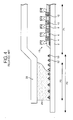
- the organic EL display device further includes a dummy insulating pattern 107 at the seal line area P3 of the non-display area P2.
- the dummy insulating pattern 107 is formed to cover the second lines 152 densely located in the seal line area P3, so that the sealant 125 is corresponded to the seal line area P3 and is uniformly formed.
- the dummy insulating pattern 107 is formed to cover the densely arranged second line 152.
- the sealant 125 is located on the dummy insulating pattern 107, so that it is possible to prevent an uneven formation of the sealant caused by the second line 152 as compared with the related art.
- the dummy insulating pattern 107 might be formed to be overlapped with the seal line area P3 of a direction adjacent to the display area P1 and to be partially further enlarged from the seal line area P3 to the display area P1 direction.
- the dummy insulating pattern 107 might be formed to be overlapped with the seal line area P2 as much as more than a half thereof.
- the dummy insulating pattern 107 is formed of an organic material identical to the insulating film 106 of the organic EL array 115 and a thickness of the dummy insulating pattern 107 is approximately 1.2 ⁇ m, and a thickness of the second line 152 is approximately 1000 ⁇ , so that the dummy insulating pattern 107 can reduce a stepped difference between the second line 152 and the substrate 102.
- the anode electrode 104 and the second line 152 are provided by depositing a transparent conductive metal material onto the substrate 102 made of a sodalime or a vulcanized glass and then patterning it by the photolithography and the etching process.
- a transparent conductive metal material such as indium-tin-oxide (ITO) or SnO 2 is used as the metal material.
- a conductive metal material such as molybdenum Mo and the like is deposited and is patterned by a photolithography process and an etching process, to thereby form the conductive metal layer 153 on the second line 152 as shown in FIG 6B.
- a photosensitive insulating material is coated on the substrate 102 having the anode electrode 104 and the second line 152 by a spin-coating method, and is patterned, to thereby form the insulating film 106 defining a light-emitting area of the display area P1 and the dummy insulating pattern 107 on the seal line area P3 as shown in FIG. 6C.
- the dummy insulating pattern 107 is formed to cover the second line 152 densely arranged on the seal line area P3, and might be formed to be partially further enlarged from the seal line area P3 to the display area P1 direction.
- a photosensitive insulating material is deposited on the substrate 102 having the insulating film 106 and the dummy insulating pattern 107, and is patterned by a photolithography process and an etching process, to thereby form a barrier rib 108 as shown in FIG. 6D.
- the barrier rib 108 is formed at a non light-emitting area to be cross with the anode electrodes 104 in order to partition a pixel.
- an organic light-emitting layer 110 is formed on the substrate 102 having the barrier rib 108 by a heat deposition, a vacuum deposition and the like using a common mask and a show mask, those are not shown.
- a metal material is deposited on the substrate 102 having the organic light-emitting layer 110, to thereby form a cathode electrode 112 as shown in FIG. 6F.
- the sealant 125 is applied to an area where the cap 128 and the substrate 102 are adhered, and then an encapsulating process is performed to make the sealant is corresponded to the seal line area P3 of the substrate 102, to thereby combine the cap 128 and the substrate 102 provided with the organic EL array 115 having the cathode electrode 112 as shown in FIG. 6G.
- the dummy insulating pattern 107 is formed to cover the second line 152 (or signal line) located at the seal line area P3, that is adhering area of both the cap and the substrate.
- the dummy insulating pattern 107 reduces a stepped difference between the substrate 102 and the second line 152, so that the sealant 125 becomes uniformly formed at the seal line area P3.
- the adhesion of the sealant 125 becomes improved, to thereby improve a packaging of the organic EL array 115.
- the dummy insulating pattern is formed to cover the second line (or signal line) located at the seal line area, so that the dummy insulating pattern reduces a stepped difference between the substrate and the second line. Accordingly, the sealant becomes uniformly formed, so that it is possible to improve a packaging of the organic EL array.
Abstract
Description
- This application claims the benefit of Korean Patent Application No. P2004-44331 filed in Korea on June 16, 2004, which is hereby incorporated by reference.
- This invention relates to an electro-luminescence display (ELD), and more particularly, to an organic electro-luminescence display device and a fabricating method thereof that are adaptive for improving an adhesion of a sealant used in an encapsulation process.
- Recently, there have been developed various flat panel display devices reduced in weight and bulk that is capable of eliminating disadvantages of a cathode ray tube (CRT). Such flat panel display devices include a liquid crystal display (LCD), a field emission display (FED), a plasma display panel (PDP) and an electro-luminescence (EL) display, etc. device. In such flat panel display devices, the PDP has the most advantage for making a large dimension screen because its structure and manufacturing process are simple, but has a drawback in that it has low light-emission efficiency and large power consumption. The LCD has a difficulty in making a large dimension screen because it is fabricated by a semiconductor process, but has an expanded demand as it is mainly used for a display device of a notebook personal computer. However, the LCD has a drawback in that it has a difficulty in making a large dimension screen and it has large power consumption due to a backlight unit. Also, the LCD has characteristics of a large light loss and a narrow viewing angle due to optical devices such as a polarizing filter, a prism sheet, a diffuser and the like. On the other hand, the EL display device is largely classified into an inorganic EL device and an organic EL device depending upon a material of a light-emitting layer, and is a self-luminous device. When compared with the above-mentioned display devices, the EL display device has advantages of a fast response speed, large light-emission efficiency, a large brightness and a large viewing angle. The organic EL display device can display a picture at approximately 10[V] and a high brightness of ten thousands of [cd/m2]. The organic EL display device is largely used for a mini type display such as mobile phone and the like.
- FIG. 1 is a schematic view showing a related art organic EL display device, and FIG. 2 is a sectional view specifically illustrating 'A' area in FIG. 1.
- Referring to FIG. 1 and FIG. 2, the related art EL display device includes: a display area P1 provided with an organic EL array; and a non-display area P2 provided with a
pad portion 25 for applying driving signals to driving electrodes at the display area P1 and a adhering area P3(or seal line area) both of acap 28 and asubstrate 2. - The display area P1 is provided with an
anode electrode 4 formed on thesubstrate 2, and acathode electrode 12 formed in a direction crossing theanode electrode 4. - A plurality of
anode electrodes 4 are provided on thesubstrate 2 in such a manner to be spaced at a desired distance from each other. Theanode electrode 4 is partially exposed, to thereby form aninsulating film 6 defining a light-emitting area on thesubstrate 2 having theanode electrode 4. On theinsulating film 6, abarrier rib 8 for making a separation of an organic light-emittinglayer 10 and thecathode electrode 12 to be formed thereon is provided. Thebarrier rib 8 is formed in a direction crossing theanode electrode 4, and has an overhang structure in which the upper portion thereof has a larger width than the lower portion thereof. The organic light-emittinglayer 10 made of an organic compound and thecathode electrode 12 are entirely deposited onto theinsulating film 6 provided with thebarrier rib 8. The organic light-emitting layer 10 is formed by depositing a hole injection layer, a hole carrier layer, a light-emitting layer, an electron carrier layer and an electron injection layer onto theanode electrode 4. - The non-display area P2 is provided with a
first line 54 extended from theanode electrode 4 at the display area P1, data pads for supplying data voltages, via thefirst line 54, to theanode electrode 4, asecond line 52 connected to thecathode electrode 12, and scan pads for supplying scan voltages via thesecond line 52. Herein, the first and thesecond lines anode electrode 4, and aconductive metal layer 53 is further formed of molybdenum and the like, on thesecond line 52 in order to reinforce a conductivity of thesecond line 52. - The data pad is connected to a tape carrier package (TCP) mounted with a first driving circuit for generating data voltages to thereby supply the data voltage to each
anode electrode 4. The scan pad is provided at each side of the data pad. The scan pad is connected to a TCP mounted with a second driving circuit for generating scan voltages, to thereby supply the scan voltage to eachcathode electrode 12. - The
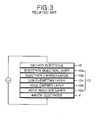
cap 28, adhered to thesubstrate 2 via thesealant 25 at the seal line area P3 of the non-display area P2, prevents theorganic EL array 15 of the display area P1 from oxygen and moisture in the area. - As shown in FIG. 3, in the related art organic EL display device having the structure as mentioned above, if a voltage is applied between the
anode electrode 4 and thecathode electrode 12, then electrons (or cathodes) generated from thecathode electrode 12 are moved, via anelectron injection layer 10a and anelectron carrier layer 10b, into a light-emitting layer 10c. On the other hand, holes (or anodes) generated from theanode electrode 4 are moved, via ahole injection layer 10e and ahole carrier layer 10d, into the light-emittinglayer 10c. - Accordingly, in the light-emitting
layer 10c, the electron and the hole supplied from theelectron carrier layer 10b and thehole carrier layer 10d are recombined to form an exiton, and the exiton is excited again to a ground state, thus a light of a fixed energy is emitted to the outside through theanode electrode 4, so that a picture is displayed. - Meanwhile, in such an organic EL display device, the
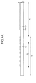
second line 52 turns around the display area P1 to connect to the scan pad, so that a plurality ofsecond lines 52 are located at the seal line area P3 as shown in FIG. 4. Thesecond lines 52 are densely arranged it is goes from the seal line area P3 to the display area P1. Accordingly, there is a problem that thesealant 25 is not uniformly at the seal line area P3 upon adhering the cap to thesubstrate 2, as shown in FIG. 4. In other words, since the densely arrangedsecond line 52 prevents that thesealant 25 is uniformly spread to the seal line area P3 upon adhering thecan 28 to the substrate, a width of thespread sealant 25 becomes uneven. - Accordingly, in a case that an adhesive power both of the
substrate 2 and thecap 28 becomes lowered and an unbalance pressure is generated at a fixed area, there is a problem of a packaging badness, i. e., thesealant 25 is partially broken. - Accordingly, it is an object of the present invention to provide an organic electro-luminescence display device and a fabricating method thereof that are adaptive for improving an adhesion of a sealant used in an encapsulation process.
- In order to achieve these and other objects of the invention, an organic electro-luminescence display device according to an embodiment of the present invention includes: a substrate provided with an organic electro-luminescence array having first and second electrodes crossing each other with having an organic light-emitting layer therebetween; a cap adhered via a sealant to a seal line area; a plurality of signal lines connected to any one of the first and the second electrodes and located on the seal line area; and a dummy insulating pattern formed to cover any one of the signal lines, wherein a portion of the dummy insulating pattern is formed on the seal line area.
- The dummy insulating pattern is overlapped with a portion of the seal line area adjacent to the organic electro-luminescence array.
- The dummy insulating pattern is overlapped with the seal line area as much as more than 1/2 of the entire width of the seal line area.
- The signal lines are arranged by a narrower distance as it is goes from the seal line area to the organic electro-luminescence array, and the dummy insulating pattern is formed to cover at least one signal line located at the seal line area adjacent to the organic electro-luminescence array.
- The dummy insulating pattern is formed to cover more than 1/2 of the signal lines.
- The organic electro-luminescence display device further includes an insulating film formed on the first electrode to define a light-emitting area, wherein the dummy insulating pattern is the same material as the insulating film.
- A method of fabricating an organic electro-luminescence display device according to an embodiment of the present invention includes: forming an organic electro-luminescence array having first and second electrodes crossing each other with having an organic light-emitting layer therebetween; providing a cap adhered via a sealant to a seal line area; forming a plurality of signal lines connected to any one of the first and the second electrodes and located on the seal line area; and forming a dummy insulating pattern to cover any one of the signal lines, wherein a portion of the dummy insulating pattern is formed on the seal line area.
- The organic electro-luminescence array includes an insulating film defining the light-emitting area by partially exposing the first electrode, and the dummy insulating pattern is simultaneously formed of the same material as the insulating film.
- These and other objects of the invention will be apparent from the following detailed description of the embodiments of the present invention with reference to the accompanying drawings, in which:
- FIG. 1 is a schematic view showing a structure of a related art organic electro-luminescence display device;
- FIG. 2 is a sectional view specifically illustrating ' A' area in FIG. 1;
- FIG. 3 is a diagram for explaining a light-emitting principle of the organic electro-luminescence display device;
- FIG. 4 is a sectional view for explaining a formation badness of the related art sealant;
- FIG. 5 is a sectional view specifically illustrating a portion of the organic electro-luminescence display device according to the present invention; and
- FIG. 6A to FIG. 6G are sectional views for sequentially explaining a method of fabricating the organic electro-luminescence display device shown in FIG. 5.
- Reference will now be made in detail to the preferred embodiments of the present invention, examples of which are illustrated in the accompanying drawings.
- Hereinafter, the preferred embodiments of the present invention will be described in detail with reference to FIGs. 5 to 6G.
- FIG. 5 is a schematic section view showing a portion of an organic electro-luminescence display device according to the present invention.
- Referring to FIG. 5, the organic EL display device according to the present invention includes: a display area P1 provided with an
organic EL array 115; and a non-display area P2 provided with a pad portion(not shown) for applying driving signals to driving electrodes at the display area P1 and a adhering area P3(or seal line area) both of acap 128 and asubstrate 102. - The display area P1 is provided with an
anode electrode 104 formed on thesubstrate 102, and acathode electrode 112 formed in a direction crossing theanode electrode 104. - A plurality of
anode electrodes 104 are provided on thesubstrate 102 in such a manner to be spaced at a desired distance from each other. Theanode electrode 104 is partially exposed, to thereby form an insulatingfilm 106 defining a light-emitting area on thesubstrate 102 having theanode electrode 104. On the insulatingfilm 106, abarrier rib 108 for making a separation of an organic light-emittinglayer 110 and thecathode electrode 112 to be formed thereon is provided. Thebarrier rib 108 is formed in a direction crossing theanode electrode 104, and has an overhang structure in which the upper portion thereof has a larger width than the lower portion thereof. The organic light-emittinglayer 110 made of an organic compound and thecathode electrode 112 are entirely deposited onto the insulatingfilm 106 provided with thebarrier rib 108. The organic light-emittinglayer 110 is formed by depositing a hole injection layer, a hole carrier layer, a light-emitting layer, an electron carrier layer and an electron injection layer onto theanode electrode 104. - The non-display area P2 is provided with a first line(not shown) extended from the
anode electrode 104 at the display area P1, data pads for supplying data voltages, via the first line, to theanode electrode 104, asecond line 152 connected to thecathode electrode 112, and scan pads for supplying scan voltages via thesecond line 152. Herein, the first line and thesecond line 152 are formed of the same transparent electrode material as theanode electrode 104, and aconductive metal layer 153 is further formed of molybdenum and the like, on thesecond line 152 in order to reinforce a conductivity of thesecond line 152. - The
cap 128, adhered to thesubstrate 102 via thesealant 125 at the seal line area P3 of the non-display area P2, prevents theorganic EL array 115 of the display area P1 from oxygen and moisture in the area. - The organic EL display device according to the present invention further includes a
dummy insulating pattern 107 at the seal line area P3 of the non-display area P2. Thedummy insulating pattern 107 is formed to cover thesecond lines 152 densely located in the seal line area P3, so that thesealant 125 is corresponded to the seal line area P3 and is uniformly formed. - More specifically, this will be described as follows.
- A portion of the
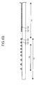
second line 152, turning around the display area P1 to connect to the scan pad, is located at the seal line area P3, especially, becomes densely arranged as it goes from the seal line area P3 to the display area P1. Herein, thedummy insulating pattern 107 is formed to cover the densely arrangedsecond line 152. And, thesealant 125 is located on thedummy insulating pattern 107, so that it is possible to prevent an uneven formation of the sealant caused by thesecond line 152 as compared with the related art. Thedummy insulating pattern 107 might be formed to be overlapped with the seal line area P3 of a direction adjacent to the display area P1 and to be partially further enlarged from the seal line area P3 to the display area P1 direction. Furthermore, thedummy insulating pattern 107 might be formed to be overlapped with the seal line area P2 as much as more than a half thereof. Meanwhile, thedummy insulating pattern 107 is formed of an organic material identical to the insulatingfilm 106 of theorganic EL array 115 and a thickness of thedummy insulating pattern 107 is approximately 1.2µm, and a thickness of thesecond line 152 is approximately 1000Å, so that thedummy insulating pattern 107 can reduce a stepped difference between thesecond line 152 and thesubstrate 102. - Hereinafter, a method of fabricating the organic EL display device will be described with reference to FIGs. 6A to 6G.
- Firstly, as shown in FIG. 6A, the
anode electrode 104 and thesecond line 152 are provided by depositing a transparent conductive metal material onto thesubstrate 102 made of a sodalime or a vulcanized glass and then patterning it by the photolithography and the etching process. Herein, indium-tin-oxide (ITO) or SnO2 is used as the metal material. - on the
substrate 102, a conductive metal material such as molybdenum Mo and the like is deposited and is patterned by a photolithography process and an etching process, to thereby form theconductive metal layer 153 on thesecond line 152 as shown in FIG 6B. - A photosensitive insulating material is coated on the
substrate 102 having theanode electrode 104 and thesecond line 152 by a spin-coating method, and is patterned, to thereby form the insulatingfilm 106 defining a light-emitting area of the display area P1 and thedummy insulating pattern 107 on the seal line area P3 as shown in FIG. 6C. Herein, thedummy insulating pattern 107 is formed to cover thesecond line 152 densely arranged on the seal line area P3, and might be formed to be partially further enlarged from the seal line area P3 to the display area P1 direction. - A photosensitive insulating material is deposited on the
substrate 102 having the insulatingfilm 106 and thedummy insulating pattern 107, and is patterned by a photolithography process and an etching process, to thereby form abarrier rib 108 as shown in FIG. 6D. Thebarrier rib 108 is formed at a non light-emitting area to be cross with theanode electrodes 104 in order to partition a pixel. - As shown in FIG. 6E, an organic light-emitting
layer 110 is formed on thesubstrate 102 having thebarrier rib 108 by a heat deposition, a vacuum deposition and the like using a common mask and a show mask, those are not shown. - A metal material is deposited on the
substrate 102 having the organic light-emittinglayer 110, to thereby form acathode electrode 112 as shown in FIG. 6F. - Thereafter, the
sealant 125 is applied to an area where thecap 128 and thesubstrate 102 are adhered, and then an encapsulating process is performed to make the sealant is corresponded to the seal line area P3 of thesubstrate 102, to thereby combine thecap 128 and thesubstrate 102 provided with theorganic EL array 115 having thecathode electrode 112 as shown in FIG. 6G. - In the organic electro-luminescence display device and a fabricating method thereof, the
dummy insulating pattern 107 is formed to cover the second line 152 (or signal line) located at the seal line area P3, that is adhering area of both the cap and the substrate. Thedummy insulating pattern 107 reduces a stepped difference between thesubstrate 102 and thesecond line 152, so that thesealant 125 becomes uniformly formed at the seal line area P3. Hereby, the adhesion of thesealant 125 becomes improved, to thereby improve a packaging of theorganic EL array 115. - As described above, in the organic electro-luminescence display device and a fabricating method thereof, the dummy insulating pattern is formed to cover the second line (or signal line) located at the seal line area, so that the dummy insulating pattern reduces a stepped difference between the substrate and the second line. Accordingly, the sealant becomes uniformly formed, so that it is possible to improve a packaging of the organic EL array.
- Although the present invention has been explained by the embodiments shown in the drawings described above, it should be understood to the ordinary skilled person in the art that the invention is not limited to the embodiments, but rather that various changes or modifications thereof are possible without departing from the spirit of the invention. Accordingly, the scope of the invention shall be determined only by the appended claims and their equivalents.
Claims (8)
- An organic electro-luminescence display device, comprising:a substrate provided with an organic electro-luminescence array having first and second electrodes crossing each other with having an organic light-emitting layer therebetween;a cap adhered via a sealant to a seal line area;a plurality of signal lines connected to any one of the first and the second electrodes and located on the seal line area; anda dummy insulating pattern formed to cover any one of the signal lines, wherein a portion of the dummy insulating pattern is formed on the seal line area.
- The organic electro-luminescence display device according to claim 1, wherein the dummy insulating pattern is overlapped with a portion of the seal line area adjacent to the organic electro-luminescence array.
- The organic electro-luminescence display device according to claim 2, wherein the dummy insulating pattern is overlapped with the seal line area as much as more than 1/2 of the entire width of the seal line area.
- The organic electro-luminescence display device according to claim 1, wherein the signal lines are arranged by a narrower distance as it is goes from the seal line area to the organic electro-luminescence array, and the dummy insulating pattern is formed to cover at least one signal line located at the seal line area adjacent to the organic electro-luminescence array.
- The organic electro-luminescence display device according to claim 4, wherein the dummy insulating pattern is formed to cover more than 1/2 of the signal lines.
- The organic electro-luminescence display device according to claim 1, further comprising an insulating film formed on the first electrode to define a light-emitting area, wherein the dummy insulating pattern is the same material as the insulating film.
- A method of fabricating an organic electro-luminescence display device, further comprising:forming an organic electro-luminescence array having first and second electrodes crossing each other with having an organic light-emitting layer therebetween;providing a cap adhered via a sealant to a seal line area;forming a plurality of signal lines connected to any one of the first and the second electrodes and located on the seal line area; andforming a dummy insulating pattern to cover any one of the signal lines, wherein a portion of the dummy insulating pattern is formed on the seal line area.
- The method according to claim 7, wherein the organic electro-luminescence array includes an insulating film defining the light-emitting area by partially exposing the first electrode, and the dummy insulating pattern is simultaneously formed of the same material as the insulating film.
Applications Claiming Priority (2)
| Application Number | Priority Date | Filing Date | Title |
|---|---|---|---|
| KR2004044331 | 2004-06-16 | ||
| KR1020040044331A KR100681022B1 (en) | 2004-06-16 | 2004-06-16 | Organic Electro Luminescence Display Device And Fabricating Method Thereof |
Publications (3)
| Publication Number | Publication Date |
|---|---|
| EP1608032A2 true EP1608032A2 (en) | 2005-12-21 |
| EP1608032A3 EP1608032A3 (en) | 2007-05-16 |
| EP1608032B1 EP1608032B1 (en) | 2011-11-23 |
Family
ID=34937427
Family Applications (1)
| Application Number | Title | Priority Date | Filing Date |
|---|---|---|---|
| EP05012738A Not-in-force EP1608032B1 (en) | 2004-06-16 | 2005-06-14 | Organic electro-luminescence display device and fabricating method thereof |
Country Status (5)
| Country | Link |
|---|---|
| US (1) | US20050280360A1 (en) |
| EP (1) | EP1608032B1 (en) |
| JP (1) | JP5057007B2 (en) |
| KR (1) | KR100681022B1 (en) |
| CN (1) | CN100592530C (en) |
Cited By (6)
| Publication number | Priority date | Publication date | Assignee | Title |
|---|---|---|---|---|
| EP1814160A2 (en) * | 2006-01-27 | 2007-08-01 | Samsung SDI Co., Ltd. | Flat panel display device and method of making the same |
| EP1814158A2 (en) * | 2006-01-27 | 2007-08-01 | Samsung SDI Co., Ltd. | Flat panel display device and method of making the same |
| US9950100B2 (en) | 2004-04-28 | 2018-04-24 | Smith & Nephew Plc | Negative pressure wound therapy dressing system |
| US10278869B2 (en) | 2002-10-28 | 2019-05-07 | Smith & Nephew Plc | Apparatus for aspirating, irrigating and cleansing wounds |
| US10328187B2 (en) | 2007-07-02 | 2019-06-25 | Smith & Nephew Plc | Systems and methods for controlling operation of negative pressure wound therapy apparatus |
| US10617801B2 (en) | 2007-08-06 | 2020-04-14 | Smith & Nephew Plc | Canister status determination |
Families Citing this family (12)
| Publication number | Priority date | Publication date | Assignee | Title |
|---|---|---|---|---|
| KR100671643B1 (en) * | 2006-01-27 | 2007-01-19 | 삼성에스디아이 주식회사 | Organic light emitting display device and a method of manufacturing thereof |
| KR100688789B1 (en) * | 2006-01-27 | 2007-03-02 | 삼성에스디아이 주식회사 | Organic light emitting display device and a method of manufacturing thereof |
| JP2007220647A (en) * | 2006-02-14 | 2007-08-30 | Samsung Sdi Co Ltd | Organic electroluminescent display device and its manufacturing method |
| KR100761174B1 (en) * | 2006-11-23 | 2007-09-21 | 엘지전자 주식회사 | Light emitting diode |
| KR100879858B1 (en) * | 2007-07-09 | 2009-01-22 | 삼성모바일디스플레이주식회사 | Organic Light Emitting Display Device |
| KR100883072B1 (en) * | 2007-07-12 | 2009-02-10 | 엘지전자 주식회사 | Display device |
| CN101789493B (en) * | 2009-12-25 | 2012-11-07 | 昆山维信诺显示技术有限公司 | Organic electroluminescent device |
| US8283853B2 (en) * | 2010-03-31 | 2012-10-09 | General Electric Company | Light-emitting device and article |
| KR102169015B1 (en) * | 2013-12-23 | 2020-10-23 | 삼성디스플레이 주식회사 | Mother substrate for organic light emitting display apparatus and organic light emitting display apparatus |
| KR102482408B1 (en) * | 2017-05-19 | 2022-12-28 | 삼성디스플레이 주식회사 | Display device |
| CN109216565B (en) | 2017-06-30 | 2021-05-18 | 昆山国显光电有限公司 | Organic electroluminescent device and preparation method thereof |
| CN109713015B (en) * | 2018-12-29 | 2021-01-22 | 苏州清越光电科技股份有限公司 | Display panel and display terminal |
Citations (4)
| Publication number | Priority date | Publication date | Assignee | Title |
|---|---|---|---|---|
| US20020000560A1 (en) * | 2000-05-31 | 2002-01-03 | Nec Corporation | Organic EL element and method of manufacturing the same |
| US6590337B1 (en) * | 1999-09-29 | 2003-07-08 | Sanyo Electric Co., Ltd. | Sealing structure for display device |
| US6624572B1 (en) * | 2000-02-17 | 2003-09-23 | Lg Electronics, Inc. | Organic electroluminescence display panel and method for sealing the same |
| WO2003096440A2 (en) * | 2002-05-07 | 2003-11-20 | Osram Opto Semiconductors Gmbh | Organic device |
Family Cites Families (17)
| Publication number | Priority date | Publication date | Assignee | Title |
|---|---|---|---|---|
| US5076667A (en) * | 1990-01-29 | 1991-12-31 | David Sarnoff Research Center, Inc. | High speed signal and power supply bussing for liquid crystal displays |
| KR100356973B1 (en) * | 1994-01-01 | 2003-01-24 | 코닌클리케 필립스 일렉트로닉스 엔.브이. | Liquid crystal display device and method for manufacturing a number of liquid crystal display devices |
| US5684555A (en) * | 1994-12-19 | 1997-11-04 | Kabushiki Kaisha Toshiba | Liquid crystal display panel |
| JP3737176B2 (en) * | 1995-12-21 | 2006-01-18 | 株式会社半導体エネルギー研究所 | Liquid crystal display |
| US5953094A (en) * | 1997-04-04 | 1999-09-14 | Sanyo Electric Co., Ltd. | Liquid crystal display device |
| JP3907804B2 (en) * | 1997-10-06 | 2007-04-18 | 株式会社半導体エネルギー研究所 | Liquid crystal display |
| TW439387B (en) * | 1998-12-01 | 2001-06-07 | Sanyo Electric Co | Display device |
| JP2002008871A (en) * | 2000-06-27 | 2002-01-11 | Tohoku Pioneer Corp | Organic electroluminescent display panel |
| US7019718B2 (en) * | 2000-07-25 | 2006-03-28 | Semiconductor Energy Laboratory Co., Ltd. | Display device |
| JP4027614B2 (en) * | 2001-03-28 | 2007-12-26 | 株式会社日立製作所 | Display device |
| JP3702858B2 (en) * | 2001-04-16 | 2005-10-05 | セイコーエプソン株式会社 | Electro-optical device and electronic apparatus |
| US6822264B2 (en) * | 2001-11-16 | 2004-11-23 | Semiconductor Energy Laboratory Co., Ltd. | Light emitting device |
| JP4156861B2 (en) * | 2002-05-07 | 2008-09-24 | ローム株式会社 | Organic EL display device and portable terminal |
| US7026660B2 (en) * | 2003-04-25 | 2006-04-11 | Osram Opto Semiconductors (Malaysia) Sdn. Bhd | Interconnection for organic devices |
| US7928654B2 (en) * | 2003-08-29 | 2011-04-19 | Semiconductor Energy Laboratory Co., Ltd. | Display device and method for manufacturing the same |
| KR100615212B1 (en) * | 2004-03-08 | 2006-08-25 | 삼성에스디아이 주식회사 | Flat display device |
| US7619258B2 (en) * | 2004-03-16 | 2009-11-17 | Semiconductor Energy Laboratory Co., Ltd. | Display device |
-
2004
- 2004-06-16 KR KR1020040044331A patent/KR100681022B1/en not_active IP Right Cessation
-
2005
- 2005-06-14 EP EP05012738A patent/EP1608032B1/en not_active Not-in-force
- 2005-06-15 US US11/152,077 patent/US20050280360A1/en not_active Abandoned
- 2005-06-15 CN CN200510076460A patent/CN100592530C/en active Active
- 2005-06-16 JP JP2005176245A patent/JP5057007B2/en active Active
Patent Citations (4)
| Publication number | Priority date | Publication date | Assignee | Title |
|---|---|---|---|---|
| US6590337B1 (en) * | 1999-09-29 | 2003-07-08 | Sanyo Electric Co., Ltd. | Sealing structure for display device |
| US6624572B1 (en) * | 2000-02-17 | 2003-09-23 | Lg Electronics, Inc. | Organic electroluminescence display panel and method for sealing the same |
| US20020000560A1 (en) * | 2000-05-31 | 2002-01-03 | Nec Corporation | Organic EL element and method of manufacturing the same |
| WO2003096440A2 (en) * | 2002-05-07 | 2003-11-20 | Osram Opto Semiconductors Gmbh | Organic device |
Cited By (15)
| Publication number | Priority date | Publication date | Assignee | Title |
|---|---|---|---|---|
| US10278869B2 (en) | 2002-10-28 | 2019-05-07 | Smith & Nephew Plc | Apparatus for aspirating, irrigating and cleansing wounds |
| US9950100B2 (en) | 2004-04-28 | 2018-04-24 | Smith & Nephew Plc | Negative pressure wound therapy dressing system |
| US10758424B2 (en) | 2004-04-28 | 2020-09-01 | Smith & Nephew Plc | Dressing and apparatus for cleansing the wounds |
| US10758425B2 (en) | 2004-04-28 | 2020-09-01 | Smith & Nephew Plc | Negative pressure wound therapy dressing system |
| US10039868B2 (en) | 2004-04-28 | 2018-08-07 | Smith & Nephew Plc | Dressing and apparatus for cleansing the wounds |
| EP1814160A3 (en) * | 2006-01-27 | 2007-10-31 | Samsung SDI Co., Ltd. | Flat panel display device and method of making the same |
| US8035300B2 (en) | 2006-01-27 | 2011-10-11 | Samsung Mobile Display Co., Ltd. | Flat panel display device and method of making the same |
| US7948177B2 (en) | 2006-01-27 | 2011-05-24 | Samsung Mobile Display Co., Ltd. | Flat panel display device with protective layer structure and method of making the same |
| EP1814160A2 (en) * | 2006-01-27 | 2007-08-01 | Samsung SDI Co., Ltd. | Flat panel display device and method of making the same |
| EP1814158A3 (en) * | 2006-01-27 | 2007-10-03 | Samsung SDI Co., Ltd. | Flat panel display device and method of making the same |
| EP1814158A2 (en) * | 2006-01-27 | 2007-08-01 | Samsung SDI Co., Ltd. | Flat panel display device and method of making the same |
| US10328187B2 (en) | 2007-07-02 | 2019-06-25 | Smith & Nephew Plc | Systems and methods for controlling operation of negative pressure wound therapy apparatus |
| US10617801B2 (en) | 2007-08-06 | 2020-04-14 | Smith & Nephew Plc | Canister status determination |
| US10994060B2 (en) | 2007-08-06 | 2021-05-04 | Smith & Nephew Plc | Canister status determination |
| US11559620B2 (en) | 2007-08-06 | 2023-01-24 | Smith & Nephew Plc | Canister status determination |
Also Published As
| Publication number | Publication date |
|---|---|
| US20050280360A1 (en) | 2005-12-22 |
| KR100681022B1 (en) | 2007-02-09 |
| JP5057007B2 (en) | 2012-10-24 |
| EP1608032B1 (en) | 2011-11-23 |
| EP1608032A3 (en) | 2007-05-16 |
| JP2006004942A (en) | 2006-01-05 |
| KR20050119277A (en) | 2005-12-21 |
| CN1713786A (en) | 2005-12-28 |
| CN100592530C (en) | 2010-02-24 |
Similar Documents
| Publication | Publication Date | Title |
|---|---|---|
| EP1608032B1 (en) | Organic electro-luminescence display device and fabricating method thereof | |
| KR100460210B1 (en) | Dual Panel Type Organic Electroluminescent Device and Method for Fabricating the same | |
| US7683538B2 (en) | Dual panel-type organic electroluminescent display device | |
| EP1598869A2 (en) | Organic electroluminescence display device and fabricating method thereof | |
| US7358664B2 (en) | Organic electro-luminescence display device having a pad portion | |
| US7221091B2 (en) | Organic electroluminescent display device and method of fabricating the same | |
| US7851994B2 (en) | Organic electro-luminescence display device with an organic electro-luminescence array and fabricating method thereof | |
| US7183708B2 (en) | Organic electro luminescence display device and fabricating method thereof | |
| US7486018B2 (en) | Organic electro-luminescence display device and fabricating method thereof | |
| KR100726942B1 (en) | Organic Electro-Luminescence Display Device And Fabricating Method Thereof | |
| KR20070067502A (en) | Organic electro-luminescence display device and fabricating method thereof | |
| KR100623450B1 (en) | Organic Electro-Luminescence Display Device And Fabricating Method Thereof | |
| KR100705270B1 (en) | Organic Electro Luminescence Display Device And Fabricating Method Thereof | |
| KR100592390B1 (en) | Organic electroluminescent display and manufacturing method | |
| KR100556697B1 (en) | Organic Electro Luminescence Device And Fabricating Method Thereof | |
| KR100726939B1 (en) | Organic Electro-Luminescence Display Device And Fabricating Method Thereof | |
| KR100726994B1 (en) | Organic Electro-Luminescence Display Device And Fabricating Method Thereof | |
| KR20060077051A (en) | Organic electro-luminescence display device and fabricating method thereof | |
| KR20050106138A (en) | Organic electro-luminescence display device and fabricating method thereof | |
| KR20070067499A (en) | Organic electro-luminescence display device and fabricating method thereof | |
| KR20070035791A (en) | Organic electro luminescence display device and method for fabricating thereof |
Legal Events
| Date | Code | Title | Description |
|---|---|---|---|
| PUAI | Public reference made under article 153(3) epc to a published international application that has entered the european phase |
Free format text: ORIGINAL CODE: 0009012 |
|
| 17P | Request for examination filed |
Effective date: 20050614 |
|
| AK | Designated contracting states |
Kind code of ref document: A2 Designated state(s): AT BE BG CH CY CZ DE DK EE ES FI FR GB GR HU IE IS IT LI LT LU MC NL PL PT RO SE SI SK TR |
|
| AX | Request for extension of the european patent |
Extension state: AL BA HR LV MK YU |
|
| PUAL | Search report despatched |
Free format text: ORIGINAL CODE: 0009013 |
|
| AK | Designated contracting states |
Kind code of ref document: A3 Designated state(s): AT BE BG CH CY CZ DE DK EE ES FI FR GB GR HU IE IS IT LI LT LU MC NL PL PT RO SE SI SK TR |
|
| AX | Request for extension of the european patent |
Extension state: AL BA HR LV MK YU |
|
| AKX | Designation fees paid |
Designated state(s): DE FR GB NL |
|
| 17Q | First examination report despatched |
Effective date: 20080124 |
|
| REG | Reference to a national code |
Ref country code: DE Ref legal event code: R079 Ref document number: 602005031303 Country of ref document: DE Free format text: PREVIOUS MAIN CLASS: H01L0051200000 Ipc: H01L0051520000 |
|
| GRAP | Despatch of communication of intention to grant a patent |
Free format text: ORIGINAL CODE: EPIDOSNIGR1 |
|
| RIC1 | Information provided on ipc code assigned before grant |
Ipc: H01L 27/32 20060101ALI20110524BHEP Ipc: H01L 51/52 20060101AFI20110524BHEP |
|
| GRAS | Grant fee paid |
Free format text: ORIGINAL CODE: EPIDOSNIGR3 |
|
| GRAA | (expected) grant |
Free format text: ORIGINAL CODE: 0009210 |
|
| AK | Designated contracting states |
Kind code of ref document: B1 Designated state(s): DE FR GB NL |
|
| REG | Reference to a national code |
Ref country code: GB Ref legal event code: FG4D |
|
| REG | Reference to a national code |
Ref country code: DE Ref legal event code: R096 Ref document number: 602005031303 Country of ref document: DE Effective date: 20120119 |
|
| REG | Reference to a national code |
Ref country code: NL Ref legal event code: VDEP Effective date: 20111123 |
|
| PG25 | Lapsed in a contracting state [announced via postgrant information from national office to epo] |
Ref country code: NL Free format text: LAPSE BECAUSE OF FAILURE TO SUBMIT A TRANSLATION OF THE DESCRIPTION OR TO PAY THE FEE WITHIN THE PRESCRIBED TIME-LIMIT Effective date: 20111123 |
|
| PLBE | No opposition filed within time limit |
Free format text: ORIGINAL CODE: 0009261 |
|
| STAA | Information on the status of an ep patent application or granted ep patent |
Free format text: STATUS: NO OPPOSITION FILED WITHIN TIME LIMIT |
|
| 26N | No opposition filed |
Effective date: 20120824 |
|
| REG | Reference to a national code |
Ref country code: DE Ref legal event code: R097 Ref document number: 602005031303 Country of ref document: DE Effective date: 20120824 |
|
| GBPC | Gb: european patent ceased through non-payment of renewal fee |
Effective date: 20120614 |
|
| REG | Reference to a national code |
Ref country code: FR Ref legal event code: ST Effective date: 20130228 |
|
| REG | Reference to a national code |
Ref country code: DE Ref legal event code: R119 Ref document number: 602005031303 Country of ref document: DE Effective date: 20130101 |
|
| PG25 | Lapsed in a contracting state [announced via postgrant information from national office to epo] |
Ref country code: DE Free format text: LAPSE BECAUSE OF NON-PAYMENT OF DUE FEES Effective date: 20130101 Ref country code: GB Free format text: LAPSE BECAUSE OF NON-PAYMENT OF DUE FEES Effective date: 20120614 Ref country code: FR Free format text: LAPSE BECAUSE OF NON-PAYMENT OF DUE FEES Effective date: 20120702 |