EP1640334A2 - An integrated lid formed on mems device - Google Patents
An integrated lid formed on mems device Download PDFInfo
- Publication number
- EP1640334A2 EP1640334A2 EP05255976A EP05255976A EP1640334A2 EP 1640334 A2 EP1640334 A2 EP 1640334A2 EP 05255976 A EP05255976 A EP 05255976A EP 05255976 A EP05255976 A EP 05255976A EP 1640334 A2 EP1640334 A2 EP 1640334A2
- Authority
- EP
- European Patent Office
- Prior art keywords
- lid
- cavity
- slide
- opening
- moving part
- Prior art date
- Legal status (The legal status is an assumption and is not a legal conclusion. Google has not performed a legal analysis and makes no representation as to the accuracy of the status listed.)
- Granted
Links
- 239000000463 material Substances 0.000 claims description 17
- 238000000034 method Methods 0.000 claims description 12
- 239000000758 substrate Substances 0.000 claims description 12
- 230000015572 biosynthetic process Effects 0.000 claims description 8
- 150000004767 nitrides Chemical class 0.000 abstract description 8
- 238000004544 sputter deposition Methods 0.000 abstract description 3
- XUIMIQQOPSSXEZ-UHFFFAOYSA-N Silicon Chemical compound [Si] XUIMIQQOPSSXEZ-UHFFFAOYSA-N 0.000 description 5
- 229910052710 silicon Inorganic materials 0.000 description 5
- 239000010703 silicon Substances 0.000 description 5
- 239000007788 liquid Substances 0.000 description 3
- 230000008569 process Effects 0.000 description 3
- 230000001133 acceleration Effects 0.000 description 2
- 239000003990 capacitor Substances 0.000 description 2
- 239000000919 ceramic Substances 0.000 description 2
- 238000010586 diagram Methods 0.000 description 2
- 239000008393 encapsulating agent Substances 0.000 description 2
- 239000002184 metal Substances 0.000 description 2
- 230000004044 response Effects 0.000 description 2
- 230000004075 alteration Effects 0.000 description 1
- 238000010276 construction Methods 0.000 description 1
- 230000007812 deficiency Effects 0.000 description 1
- 238000005530 etching Methods 0.000 description 1
- 238000004519 manufacturing process Methods 0.000 description 1
- 230000007246 mechanism Effects 0.000 description 1
- 239000002245 particle Substances 0.000 description 1
- 238000002161 passivation Methods 0.000 description 1
- 238000000059 patterning Methods 0.000 description 1
- 238000005498 polishing Methods 0.000 description 1
- 229910021420 polycrystalline silicon Inorganic materials 0.000 description 1
- 229920005591 polysilicon Polymers 0.000 description 1
- 238000007789 sealing Methods 0.000 description 1
- 239000007787 solid Substances 0.000 description 1
- 238000006467 substitution reaction Methods 0.000 description 1
Images


Classifications
-
- B—PERFORMING OPERATIONS; TRANSPORTING
- B81—MICROSTRUCTURAL TECHNOLOGY
- B81C—PROCESSES OR APPARATUS SPECIALLY ADAPTED FOR THE MANUFACTURE OR TREATMENT OF MICROSTRUCTURAL DEVICES OR SYSTEMS
- B81C1/00—Manufacture or treatment of devices or systems in or on a substrate
- B81C1/00015—Manufacture or treatment of devices or systems in or on a substrate for manufacturing microsystems
- B81C1/00261—Processes for packaging MEMS devices
- B81C1/00333—Aspects relating to packaging of MEMS devices, not covered by groups B81C1/00269 - B81C1/00325
-
- B—PERFORMING OPERATIONS; TRANSPORTING
- B81—MICROSTRUCTURAL TECHNOLOGY
- B81C—PROCESSES OR APPARATUS SPECIALLY ADAPTED FOR THE MANUFACTURE OR TREATMENT OF MICROSTRUCTURAL DEVICES OR SYSTEMS
- B81C2203/00—Forming microstructural systems
- B81C2203/01—Packaging MEMS
- B81C2203/0136—Growing or depositing of a covering layer
-
- B—PERFORMING OPERATIONS; TRANSPORTING
- B81—MICROSTRUCTURAL TECHNOLOGY
- B81C—PROCESSES OR APPARATUS SPECIALLY ADAPTED FOR THE MANUFACTURE OR TREATMENT OF MICROSTRUCTURAL DEVICES OR SYSTEMS
- B81C2203/00—Forming microstructural systems
- B81C2203/01—Packaging MEMS
- B81C2203/0145—Hermetically sealing an opening in the lid
-
- B—PERFORMING OPERATIONS; TRANSPORTING
- B81—MICROSTRUCTURAL TECHNOLOGY
- B81C—PROCESSES OR APPARATUS SPECIALLY ADAPTED FOR THE MANUFACTURE OR TREATMENT OF MICROSTRUCTURAL DEVICES OR SYSTEMS
- B81C2203/00—Forming microstructural systems
- B81C2203/01—Packaging MEMS
- B81C2203/0163—Reinforcing a cap, e.g. with ribs
Definitions
- the present invention is directed, in general, to integrated circuit structures and, more specifically, to micro-electro-mechanical system structures.
- Micro-electro-mechanical system (MEMS) devices typically include at least one freely movable structure within a recess formed in a substrate and covered by a "lid" or overlying layer.
- the lid includes openings therethrough to allow etchant to be employed in removing a sacrificial material fixing the movable structure in place until the enclosure surrounding the structure is completely formed.
- Such openings if not too large, may be subsequently sealed by sputtering metal into the opening.
- openings through the lid that are too small may not allow sufficient etchant to pass through to etch the structure as desired. Accordingly, the size of the openings and/or the time required to perform an etch through the openings is constrained.
- MEMS micro-electro-mechanical system
- FIGURES 1 through 8C are diagrams illustrating formation of a micro-electro-mechanical system device structure having an integrated lid supported by pillars and having openings sealed by slides according to one embodiment of the present invention.
- FIGURES 1 through 8C discussed below, and the various embodiments used to describe the principles of the present invention in this patent document are by way of illustration only and should not be construed in any way to limit the scope of the invention. Those skilled in the art will understand that the principles of the present invention may be implemented in any suitably arranged device.
- FIGURES 1 through 8C are diagrams illustrating formation of a micro-electro-mechanical system device structure having an integrated lid supported by pillars and having openings sealed by slides according to one embodiment of the present invention.
- a MEMS device nor the complete process for formation of a MEMS device are depicted or described herein. Instead, for simplicity and clarity, only so much of the structure of a MEMS device and the process for formation of such a device as are unique to the present invention or necessary for an understanding of the present invention are depicted and described.
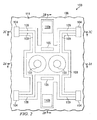
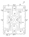
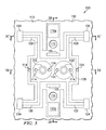
- FIGURE 1A is a plan view of a partially formed MEMS device structure.
- FIGURES 1A, 1B and 1C are cross-sectional views of the structure depicted in FIGURE 1 taken at section lines A-A, B-B and C-C, respectively.
- the same views of the device structure at different stages of processing are depicted in FIGURES 2 and 2A-2C, 3 and 3A-3C, etc.
- MEMS device structure 100 is formed by patterning recesses 101 in a silicon substrate 102, within which moveable structures will be formed, and leaving elevated regions 103-106.
- a sacrificial oxide material 107 is formed at the bottom of the recesses 101, and polysilicon is deposited thereon and selectively patterned to form movable parts 108, 109 and 110a-110b.
- the structure for the movable parts 108, 109 and 110a-110b is simply patterned from the silicon substrate 102 at the same time that recesses 101 are formed, and extend all the way to the bottom of the recesses 101 in the same manner the elevated regions 103-106.
- the MEMS device structure 100 depicted in the exemplary embodiment is a portion of an accelerometer.
- the accelerometer includes an inertia element or body 108, tethers 109 and anchors 104, where the body 108 and tethers 109 are, at the completion of formation of the MEMS device, freely movable.
- tethers 109 flex to allow movement of body 108 in response to acceleration of the MEMS device structure.
- Body 108 forms a capacitor with one or more other structures, with a capacitance that varies with movement of body 108 in response to acceleration of the integrated circuit containing the MEMS device structure 100.
- anchors 104 are electrically connected to body 108
- electrodes 105 are electrically isolated from body 108. Accordingly, one of body 108 and electrodes 105 may be connected to power and the other connected to ground to work as a variable capacitor.
- the accelerometer body 108 should preferably have a large area and significant mass, but need not necessarily be solid. Accordingly, in the present invention, pillars 103 are formed within openings through the body 108. These pillars 103 will provide support for the integrated lids as described in further detail below. In addition, movable parts 110a and 110b will form slides in the final MEMS device structure that may be moved by applying a voltage to electrodes 105 to seal large openings, also as described in further detail below.
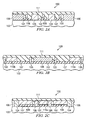
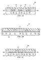
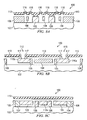
- the grooves between elevated regions 103-106 and movable parts 108, 109 and 110a-110b is backfilled with additional sacrificial oxide 111 as illustrated in the cross-sectional views of FIGURES 2A-2C, with the MEMS device structure 100, covered by the oxide 111, being shown in phantom in the plan view FIGURE 2.
- the oxide 111 may be conformally deposited, but is then preferably planarized by chemical-mechanical polishing (CMP) or another planarization process. In the example shown, some thickness of oxide 111 remains overlying the tops of elevated regions 103-106 and movable parts 108, 109 and 110a-110b after planarization.
- CMP chemical-mechanical polishing
- openings 112 are etched through the remaining thickness of oxide 111 over pillars 103 as shown in FIGURES 3 and 3A-3C.
- a nitride passivation layer 113 is then formed over the entire structure as depicted in FIGURES 4 and 4A-4C, in contact with the exposed upper surfaces of pillars 103. Nitride 113 will form the integrated lid over the MEMS device structure, supported by pillars 103 in the area over the accelerometer body in the exemplary embodiment.
- small openings 114 through nitride 113 are then formed over the grooves defining the MEMS device structure, while large openings 115, about 3 microns ( ⁇ m) in diameter, are formed through the nitride 113 in the regions adjacent to slides 110a-110b.
- Etchant is then introduced through the openings 114-115, removing the sacrificial oxide 111 as illustrated in FIGURES 6 and 6A-6C.
- a sacrificial oxide 107 was formed under the movable parts, the etchant is also employed to remove that oxide. If no sacrificial oxide 107 was employed, and the movable parts were instead patterned directly from the silicon substrate, a directionally preferential etchant is introduced through openings 114-115 to remove about a 0.5 ⁇ m thickness of silicon at the bottom of the cavities. In either event, this etch should completely undercut the movable parts (body 108, tethers 109 and slides 110a-110b) without completely undercutting the (wider) pillars 103, anchors 104, electrodes 105, and elevated regions 106 as illustrated in FIGURES 7 and 7A-7C.
- the pillars 103 may be formed of the sacrificial oxide material rather than from the substrate, with a width sufficient to prevent the pillars from being completely undercut when the etch is performed to undercut the (narrower) movable parts.
- pillars 103, anchors 104, electrodes 105, and elevated regions 106 should all be wider than the widest portions of body 108, tethers 109 and slides 110a-110b, so that those "fixed" structures are not completely undercut by the directionally preferential etch.
- the thickness of the undercut movable parts is preferably about 3-4 ⁇ m, but may be up to 10-20 ⁇ m.
- Electrodes 105 which may necessitate a hole, not shown, opened through nitride lid 111, or alternatively may be accomplished using conductive structures, also not shown, within the substrate and connected to the bottom of electrodes 105.
- the voltage causes slides 110a-110b to move beneath the large openings as illustrated in FIGURES 8 and 8A-8C.
- Metal or other deposited material is then sputtered to form plugs 116 within the small openings and seals 117 between the slides 110a-110b and nitride lid 111.
- slides 110a-110b are shown as completely disconnected from a remainder of the MEMS device structure 100.
- the slides may in fact be connected by a relatively thin strip of material to a portion of the "frame" (i.e., the elevated regions 106 surrounding the accelerometer) similar to tethers 109, and move beneath the large openings by rotation rather than by translation.
- latches may be formed to retain the slides in place after the slides are moved beneath the opening.
- a ratchet-type pawl-and-catch latch, a pair of detents catching protrusions on biased arms extending from either side of the slide, or any other suitable mechanical latching mechanism may be employed for that purpose.
- the present invention allows MEMS devices having elements with a large but not necessarily continuous area to be formed beneath an integrated lid by providing pillars to support the lid, increasing mechanical strength of the lid against breakage.
- the MEMS device structure is sealed during wafer fabrication without bonding another silicon substrate or ceramic lid over the cavities in which the movable parts are formed.
- the device may be further sealed with a liquid encapsulant prior to singulation.
- the present invention also allows large openings to be formed through the integrated lid to facilitate introduction of the etchant(s) required to separate movable structures from adjacent and/or underlying regions, with slides provided to allow the lid to be sealed against particles and liquids once the MEMS device formation is complete. Larger MEMS devices are possible, since the etchant openings limit the size of structures that may be undercut. Any additional masks required to form the slide and/or additional steps required to, for instance, apply the liquid encapsulant are offset by the processing savings from not using another substrate or a ceramic lid to sealing the MEMS device.
Abstract
Description
- The present invention is directed, in general, to integrated circuit structures and, more specifically, to micro-electro-mechanical system structures.
- Micro-electro-mechanical system (MEMS) devices typically include at least one freely movable structure within a recess formed in a substrate and covered by a "lid" or overlying layer. Often the lid includes openings therethrough to allow etchant to be employed in removing a sacrificial material fixing the movable structure in place until the enclosure surrounding the structure is completely formed. Such openings, if not too large, may be subsequently sealed by sputtering metal into the opening. However, openings through the lid that are too small may not allow sufficient etchant to pass through to etch the structure as desired. Accordingly, the size of the openings and/or the time required to perform an etch through the openings is constrained.
- In addition, if the area that must be covered by an unsupported portion of the lid is too large, the lid becomes fragile or prone to deformation, fracture or breakage. In a worst case, problems with the lid may potentially interfere with free movement of MEMS device structure. A large number of small openings through the lid merely increases the fragility of the lid.
- There is, therefore, a need in the art for an improved lid for MEMS device structures.
- To address the above-discussed deficiencies of the prior art, it is a primary object of the present invention to provide, for use in a micro-electro-mechanical system (MEMS) device structure, an integrated lid formed from a nitride layer deposited over a cavity containing movable parts for the device. Pillars are formed through openings within large area movable parts to support the lid over those parts. Slides are formed and moved under large etchant openings through the lid to allow the openings to be sealed by sputtering.
- The foregoing has outlined rather broadly the features and technical advantages of the present invention so that those skilled in the art may better understand the detailed description of the invention that follows. Additional features and advantages of the invention will be described hereinafter that form the subject of the claims of the invention. Those skilled in the art will appreciate that they may readily use the conception and the specific embodiment disclosed as a basis for modifying or designing other structures for carrying out the same purposes of the present invention. Those skilled in the art will also realize that such equivalent constructions do not depart from the spirit and scope of the invention in its broadest form.
- Before undertaking the DETAILED DESCRIPTION OF THE INVENTION below, it may be advantageous to set forth definitions of certain words or phrases used throughout this patent document: the terms "include" and "comprise," as well as derivatives thereof, mean inclusion without limitation; the term "or" is inclusive, meaning and/or; the phrases "associated with" and "associated therewith," as well as derivatives thereof, may mean to include, be included within, interconnect with, contain, be contained within, connect to or with, couple to or with, be communicable with, cooperate with, interleave, juxtapose, be proximate to, be bound to or with, have, have a property of, or the like; and the term "controller" means any device, system or part thereof that controls at least one operation, whether such a device is implemented in hardware, firmware, software or some combination of at least two of the same. It should be noted that the functionality associated with any particular controller may be centralized or distributed, whether locally or remotely. Definitions for certain words and phrases are provided throughout this patent document, and those of ordinary skill in the art will understand that such definitions apply in many, if not most, instances to prior as well as future uses of such defined words and phrases.
- For a more complete understanding of the present invention, and the advantages thereof, reference is now made to the following descriptions taken in conjunction with the accompanying drawings, wherein like numbers designate like objects, and in which:
- FIGURES 1 through 8C are diagrams illustrating formation of a micro-electro-mechanical system device structure having an integrated lid supported by pillars and having openings sealed by slides according to one embodiment of the present invention.
- FIGURES 1 through 8C, discussed below, and the various embodiments used to describe the principles of the present invention in this patent document are by way of illustration only and should not be construed in any way to limit the scope of the invention. Those skilled in the art will understand that the principles of the present invention may be implemented in any suitably arranged device.
- FIGURES 1 through 8C are diagrams illustrating formation of a micro-electro-mechanical system device structure having an integrated lid supported by pillars and having openings sealed by slides according to one embodiment of the present invention. Those skilled in the art will recognize that neither the complete structure of a MEMS device nor the complete process for formation of a MEMS device are depicted or described herein. Instead, for simplicity and clarity, only so much of the structure of a MEMS device and the process for formation of such a device as are unique to the present invention or necessary for an understanding of the present invention are depicted and described.
- FIGURE 1A is a plan view of a partially formed MEMS device structure. FIGURES 1A, 1B and 1C are cross-sectional views of the structure depicted in FIGURE 1 taken at section lines A-A, B-B and C-C, respectively. The same views of the device structure at different stages of processing are depicted in FIGURES 2 and 2A-2C, 3 and 3A-3C, etc.
-
MEMS device structure 100 is formed bypatterning recesses 101 in asilicon substrate 102, within which moveable structures will be formed, and leaving elevated regions 103-106. In the example depicted, asacrificial oxide material 107 is formed at the bottom of therecesses 101, and polysilicon is deposited thereon and selectively patterned to formmovable parts movable parts silicon substrate 102 at the same time thatrecesses 101 are formed, and extend all the way to the bottom of therecesses 101 in the same manner the elevated regions 103-106. - The
MEMS device structure 100 depicted in the exemplary embodiment is a portion of an accelerometer. The accelerometer includes an inertia element orbody 108, tethers 109 andanchors 104, where thebody 108 andtethers 109 are, at the completion of formation of the MEMS device, freely movable. In operation, tethers 109 flex to allow movement ofbody 108 in response to acceleration of the MEMS device structure.Body 108 forms a capacitor with one or more other structures, with a capacitance that varies with movement ofbody 108 in response to acceleration of the integrated circuit containing theMEMS device structure 100. For example, whileanchors 104 are electrically connected tobody 108,electrodes 105 are electrically isolated frombody 108. Accordingly, one ofbody 108 andelectrodes 105 may be connected to power and the other connected to ground to work as a variable capacitor. - The
accelerometer body 108 should preferably have a large area and significant mass, but need not necessarily be solid. Accordingly, in the present invention,pillars 103 are formed within openings through thebody 108. Thesepillars 103 will provide support for the integrated lids as described in further detail below. In addition,movable parts electrodes 105 to seal large openings, also as described in further detail below. - The grooves between elevated regions 103-106 and
movable parts sacrificial oxide 111 as illustrated in the cross-sectional views of FIGURES 2A-2C, with theMEMS device structure 100, covered by theoxide 111, being shown in phantom in the plan view FIGURE 2. Theoxide 111 may be conformally deposited, but is then preferably planarized by chemical-mechanical polishing (CMP) or another planarization process. In the example shown, some thickness ofoxide 111 remains overlying the tops of elevated regions 103-106 andmovable parts - In the exemplary embodiment,
openings 112 are etched through the remaining thickness ofoxide 111 overpillars 103 as shown in FIGURES 3 and 3A-3C. - A
nitride passivation layer 113 is then formed over the entire structure as depicted in FIGURES 4 and 4A-4C, in contact with the exposed upper surfaces ofpillars 103. Nitride 113 will form the integrated lid over the MEMS device structure, supported bypillars 103 in the area over the accelerometer body in the exemplary embodiment. - As illustrated in FIGURES 5 and 5A-5C,
small openings 114 throughnitride 113 are then formed over the grooves defining the MEMS device structure, whilelarge openings 115, about 3 microns (µm) in diameter, are formed through thenitride 113 in the regions adjacent toslides 110a-110b. Etchant is then introduced through the openings 114-115, removing thesacrificial oxide 111 as illustrated in FIGURES 6 and 6A-6C. - If a
sacrificial oxide 107 was formed under the movable parts, the etchant is also employed to remove that oxide. If nosacrificial oxide 107 was employed, and the movable parts were instead patterned directly from the silicon substrate, a directionally preferential etchant is introduced through openings 114-115 to remove about a 0.5 µm thickness of silicon at the bottom of the cavities. In either event, this etch should completely undercut the movable parts (body 108, tethers 109 andslides 110a-110b) without completely undercutting the (wider)pillars 103,anchors 104,electrodes 105, and elevatedregions 106 as illustrated in FIGURES 7 and 7A-7C. In one embodiment, thepillars 103 may be formed of the sacrificial oxide material rather than from the substrate, with a width sufficient to prevent the pillars from being completely undercut when the etch is performed to undercut the (narrower) movable parts. - If no sacrificial oxide is used beneath the movable parts,
pillars 103,anchors 104,electrodes 105, and elevatedregions 106 should all be wider than the widest portions ofbody 108, tethers 109 andslides 110a-110b, so that those "fixed" structures are not completely undercut by the directionally preferential etch. The thickness of the undercut movable parts is preferably about 3-4 µm, but may be up to 10-20 µm. - After the etching is completed and the etchant is removed, a voltage is applied to
electrodes 105, which may necessitate a hole, not shown, opened throughnitride lid 111, or alternatively may be accomplished using conductive structures, also not shown, within the substrate and connected to the bottom ofelectrodes 105. The voltage causesslides 110a-110b to move beneath the large openings as illustrated in FIGURES 8 and 8A-8C. Metal or other deposited material is then sputtered to formplugs 116 within the small openings andseals 117 between theslides 110a-110b andnitride lid 111. - In the exemplary embodiment, slides 110a-110b are shown as completely disconnected from a remainder of the
MEMS device structure 100. In an alternative embodiment, however, the slides may in fact be connected by a relatively thin strip of material to a portion of the "frame" (i.e., theelevated regions 106 surrounding the accelerometer) similar totethers 109, and move beneath the large openings by rotation rather than by translation. In either cases, latches (not shown) may be formed to retain the slides in place after the slides are moved beneath the opening. A ratchet-type pawl-and-catch latch, a pair of detents catching protrusions on biased arms extending from either side of the slide, or any other suitable mechanical latching mechanism may be employed for that purpose. - The present invention allows MEMS devices having elements with a large but not necessarily continuous area to be formed beneath an integrated lid by providing pillars to support the lid, increasing mechanical strength of the lid against breakage. The MEMS device structure is sealed during wafer fabrication without bonding another silicon substrate or ceramic lid over the cavities in which the movable parts are formed. The device may be further sealed with a liquid encapsulant prior to singulation.
- The present invention also allows large openings to be formed through the integrated lid to facilitate introduction of the etchant(s) required to separate movable structures from adjacent and/or underlying regions, with slides provided to allow the lid to be sealed against particles and liquids once the MEMS device formation is complete. Larger MEMS devices are possible, since the etchant openings limit the size of structures that may be undercut. Any additional masks required to form the slide and/or additional steps required to, for instance, apply the liquid encapsulant are offset by the processing savings from not using another substrate or a ceramic lid to sealing the MEMS device.
- Although the present invention has been described in detail, those skilled in the art will understand that various changes, substitutions, variations, enhancements, nuances, gradations, lesser forms, alterations, revisions, improvements and knock-offs of the invention disclosed herein may be made without departing from the spirit and scope of the invention in its broadest form.
Claims (16)
- An integrated circuit structure comprising:a cavity within a substrate;an integrated lid over the cavity;a first movable element disposed within the cavity, the first movable element having an opening therethrough and adapted for physical movement in at least one direction within the cavity; anda pillar extending from a bottom of the cavity through the opening in the first movable element to an inner surface of the integrated lid.
- The integrated circuit structure according to claim 1, further comprising:an opening through the lid, the opening sealed by a second movable element within the cavity disposed beneath the opening through the lid and a material formed between the second movable element and the lid.
- An integrated circuit structure comprising:a cavity within a substrate;an integrated lid over the cavity, the lid having an opening therethrough;a slide within the cavity disposed beneath the opening through the lid; anda material formed between the slide and the lid,wherein the opening through the lid is sealed by the slide and the material formed between the slide and the lid.
- The integrated circuit structure according to claim 3, further comprising:a moving part disposed within the cavity, the moving part having an opening therethrough and adapted to be selectively capable of physical movement in at least one direction within the cavity; anda pillar extending from a bottom of the cavity through the opening in the moving part to an inner surface of the integrated lid.
- The integrated circuit structure according to any preceding claim, wherein the pillar has a width greater than a widest portion of the moving part or of the first movable element.
- The integrated circuit structure according to any preceding claim, wherein, prior to formation of the material between the slide or the second movable element and the lid, the slide or second movable element is selectively movable between a first position within the cavity wherein the slide or the second movable element is not disposed beneath the opening through the lid and a second position within the cavity wherein the slide or second movable element is disposed beneath the opening through the lid.
- The integrated circuit structure according to any preceding claim, wherein the slide or second movable element is tethered to a sidewall of the cavity.
- The integrated circuit structure according to any preceding claim, wherein the second movable element or slide is secured in position beneath the opening through the lid by at least one latch.
- The integrated circuit structure according to any preceding claim, further comprising:a sacrificial material within the cavity between the moving part or the first movable element and at least one of sidewalls of the cavity, the bottom of the cavity and the lid, wherein the moving part is capable of physical movement in the at least one direction within the cavity upon removal of the sacrificial material and any other sacrificial material within the cavity adjacent to the moving part.
- A method of forming an integrated circuit structure, the method comprising:forming a cavity within a substrate;forming a moving part within the cavity, the moving part having an opening therethrough and adapted for physical movement in at least one direction within the cavity;forming an integrated lid over the cavity; andforming a pillar extending from a bottom of the cavity through the opening in the moving part to an inner surface of the integrated lid.
- The method according to claim 10, further comprising:forming the pillar with a width greater than a widest portion of the moving part.
- The method according to claim 10 or 11, further comprising:forming a sacrificial material within the cavity between the moving part and at least one of sidewalls of the cavity, the bottom of the cavity, and the lid, wherein the moving part is capable of physical movement in the at least one direction within the cavity upon removal of all sacrificial material within the cavity adjacent to the moving part.
- A method of forming an integrated circuit structure, the method comprising:forming a cavity within a substrate;forming an integrated lid over the cavity, the lid having an opening therethrough;forming a slide within the cavity disposed beneath the opening through the lid; andforming a material between the slide and the lid,wherein the opening through the lid is sealed by the slide and the material formed between the slide and the lid.
- The method according to claim 13, wherein, prior to formation of the material between the slide and the lid, the slide is selectively movable between a first position within the cavity wherein the slide is not disposed beneath the opening through the lid and a second position within the cavity wherein the slide is disposed beneath the opening through the lid.
- The method according to claim 13 or 14, wherein the slide is tethered to a sidewall of the cavity.
- The method according to claim 13, 14 or 15, wherein the slide is secured in position beneath the opening through the lid by at least one latch.
Applications Claiming Priority (1)
| Application Number | Priority Date | Filing Date | Title |
|---|---|---|---|
| US10/952,183 US7098065B2 (en) | 2004-09-28 | 2004-09-28 | Integrated lid formed on MEMS device |
Publications (3)
| Publication Number | Publication Date |
|---|---|
| EP1640334A2 true EP1640334A2 (en) | 2006-03-29 |
| EP1640334A3 EP1640334A3 (en) | 2006-05-17 |
| EP1640334B1 EP1640334B1 (en) | 2009-11-25 |
Family
ID=35623700
Family Applications (1)
| Application Number | Title | Priority Date | Filing Date |
|---|---|---|---|
| EP05255976A Active EP1640334B1 (en) | 2004-09-28 | 2005-09-26 | An integrated lid formed on mems device |
Country Status (3)
| Country | Link |
|---|---|
| US (1) | US7098065B2 (en) |
| EP (1) | EP1640334B1 (en) |
| DE (1) | DE602005017858D1 (en) |
Cited By (1)
| Publication number | Priority date | Publication date | Assignee | Title |
|---|---|---|---|---|
| WO2012141854A1 (en) * | 2011-04-14 | 2012-10-18 | Robert Bosch Gmbh | Mems package or sensor package with intra-cap electrical via and method thereof |
Families Citing this family (7)
| Publication number | Priority date | Publication date | Assignee | Title |
|---|---|---|---|---|
| US7585744B2 (en) * | 2003-12-08 | 2009-09-08 | Freescale Semiconductor, Inc. | Method of forming a seal for a semiconductor device |
| JP4726927B2 (en) * | 2008-06-19 | 2011-07-20 | 株式会社日立製作所 | Integrated microelectromechanical system and manufacturing method thereof |
| WO2010006065A2 (en) * | 2008-07-08 | 2010-01-14 | Wispry, Inc. | Thin-film lid mems devices and methods |
| WO2010111601A2 (en) * | 2009-03-26 | 2010-09-30 | Semprius, Inc. | Methods of forming printable integrated circuit devices and devices formed thereby |
| US8648432B2 (en) * | 2011-11-28 | 2014-02-11 | Texas Instruments Deutschland Gmbh | Fully embedded micromechanical device, system on chip and method for manufacturing the same |
| JP6331551B2 (en) * | 2014-03-25 | 2018-05-30 | セイコーエプソン株式会社 | MEMS device |
| US11807520B2 (en) * | 2021-06-23 | 2023-11-07 | Taiwan Semiconductor Manufacturing Company Ltd. | Semiconductor structure and method for manufacturing thereof |
Citations (6)
| Publication number | Priority date | Publication date | Assignee | Title |
|---|---|---|---|---|
| WO1995009366A1 (en) * | 1993-09-27 | 1995-04-06 | Siemens Aktiengesellschaft | Micromechanical device and process for producing the same |
| US5417235A (en) * | 1993-07-28 | 1995-05-23 | Regents Of The University Of Michigan | Integrated microvalve structures with monolithic microflow controller |
| US5441597A (en) * | 1992-12-01 | 1995-08-15 | Honeywell Inc. | Microstructure gas valve control forming method |
| US5834332A (en) * | 1995-03-17 | 1998-11-10 | Siemens Aktiengesellschaft | Micromechanical semiconductor components and manufacturing method therefor |
| US5992233A (en) * | 1996-05-31 | 1999-11-30 | The Regents Of The University Of California | Micromachined Z-axis vibratory rate gyroscope |
| DE10005555A1 (en) * | 2000-02-09 | 2001-08-16 | Bosch Gmbh Robert | Micromechanical component and corresponding manufacturing method |
Family Cites Families (4)
| Publication number | Priority date | Publication date | Assignee | Title |
|---|---|---|---|---|
| US5181156A (en) * | 1992-05-14 | 1993-01-19 | Motorola Inc. | Micromachined capacitor structure and method for making |
| US7153717B2 (en) * | 2000-05-30 | 2006-12-26 | Ic Mechanics Inc. | Encapsulation of MEMS devices using pillar-supported caps |
| JP4156946B2 (en) * | 2003-02-26 | 2008-09-24 | 三菱電機株式会社 | Acceleration sensor |
| US7585744B2 (en) * | 2003-12-08 | 2009-09-08 | Freescale Semiconductor, Inc. | Method of forming a seal for a semiconductor device |
-
2004
- 2004-09-28 US US10/952,183 patent/US7098065B2/en active Active
-
2005
- 2005-09-26 DE DE602005017858T patent/DE602005017858D1/en active Active
- 2005-09-26 EP EP05255976A patent/EP1640334B1/en active Active
Patent Citations (6)
| Publication number | Priority date | Publication date | Assignee | Title |
|---|---|---|---|---|
| US5441597A (en) * | 1992-12-01 | 1995-08-15 | Honeywell Inc. | Microstructure gas valve control forming method |
| US5417235A (en) * | 1993-07-28 | 1995-05-23 | Regents Of The University Of Michigan | Integrated microvalve structures with monolithic microflow controller |
| WO1995009366A1 (en) * | 1993-09-27 | 1995-04-06 | Siemens Aktiengesellschaft | Micromechanical device and process for producing the same |
| US5834332A (en) * | 1995-03-17 | 1998-11-10 | Siemens Aktiengesellschaft | Micromechanical semiconductor components and manufacturing method therefor |
| US5992233A (en) * | 1996-05-31 | 1999-11-30 | The Regents Of The University Of California | Micromachined Z-axis vibratory rate gyroscope |
| DE10005555A1 (en) * | 2000-02-09 | 2001-08-16 | Bosch Gmbh Robert | Micromechanical component and corresponding manufacturing method |
Cited By (2)
| Publication number | Priority date | Publication date | Assignee | Title |
|---|---|---|---|---|
| WO2012141854A1 (en) * | 2011-04-14 | 2012-10-18 | Robert Bosch Gmbh | Mems package or sensor package with intra-cap electrical via and method thereof |
| US8878314B2 (en) | 2011-04-14 | 2014-11-04 | Robert Bosch Gmbh | MEMS package or sensor package with intra-cap electrical via and method thereof |
Also Published As
| Publication number | Publication date |
|---|---|
| US7098065B2 (en) | 2006-08-29 |
| DE602005017858D1 (en) | 2010-01-07 |
| EP1640334B1 (en) | 2009-11-25 |
| US20060065961A1 (en) | 2006-03-30 |
| EP1640334A3 (en) | 2006-05-17 |
Similar Documents
| Publication | Publication Date | Title |
|---|---|---|
| EP1640334B1 (en) | An integrated lid formed on mems device | |
| US9938138B2 (en) | MEMS device structure with a capping structure | |
| JP4438786B2 (en) | MEMS vibrator and manufacturing method thereof | |
| CN110636422B (en) | Semiconductor device and method of forming the same | |
| EP2297025B1 (en) | Mems devices | |
| US7919346B2 (en) | Micromechanical component and manufacturing method | |
| US9266719B2 (en) | Methods of manufacture MEMS devices | |
| US20060157807A1 (en) | Three dimensional high aspect ratio micromachining | |
| EP1712514A2 (en) | Method for forming anti-stiction bumps on a micro-electro mechanical structure | |
| US7524767B2 (en) | Method for manufacturing a micro-electro-mechanical structure | |
| US20200346919A1 (en) | Mems apparatus with anti-stiction layer | |
| KR102202821B1 (en) | Method for forming multi-depth mems package | |
| US6242363B1 (en) | Method of etching a wafer layer using a sacrificial wall to form vertical sidewall | |
| CN116199182B (en) | Semiconductor device and manufacturing method thereof | |
| TWI606007B (en) | Micro-eletromechanical element using composite substrate and manufacturing method thereof | |
| CN116216630B (en) | Semiconductor device and manufacturing method thereof | |
| US7674392B2 (en) | Method of fabricating a hinge | |
| CN112875641A (en) | Integrated structure of MEMS device and circuit device and manufacturing method thereof | |
| CN112875642A (en) | MEMS device and method of manufacturing the same | |
| JPH06151889A (en) | Semiconductor device | |
| CN116534789A (en) | MEMS device and preparation method thereof |
Legal Events
| Date | Code | Title | Description |
|---|---|---|---|
| PUAI | Public reference made under article 153(3) epc to a published international application that has entered the european phase |
Free format text: ORIGINAL CODE: 0009012 |
|
| AK | Designated contracting states |
Kind code of ref document: A2 Designated state(s): AT BE BG CH CY CZ DE DK EE ES FI FR GB GR HU IE IS IT LI LT LU LV MC NL PL PT RO SE SI SK TR |
|
| AX | Request for extension of the european patent |
Extension state: AL BA HR MK YU |
|
| PUAL | Search report despatched |
Free format text: ORIGINAL CODE: 0009013 |
|
| AK | Designated contracting states |
Kind code of ref document: A3 Designated state(s): AT BE BG CH CY CZ DE DK EE ES FI FR GB GR HU IE IS IT LI LT LU LV MC NL PL PT RO SE SI SK TR |
|
| AX | Request for extension of the european patent |
Extension state: AL BA HR MK YU |
|
| 17P | Request for examination filed |
Effective date: 20061101 |
|
| 17Q | First examination report despatched |
Effective date: 20061206 |
|
| AKX | Designation fees paid |
Designated state(s): DE FR GB IT |
|
| GRAP | Despatch of communication of intention to grant a patent |
Free format text: ORIGINAL CODE: EPIDOSNIGR1 |
|
| GRAS | Grant fee paid |
Free format text: ORIGINAL CODE: EPIDOSNIGR3 |
|
| GRAA | (expected) grant |
Free format text: ORIGINAL CODE: 0009210 |
|
| AK | Designated contracting states |
Kind code of ref document: B1 Designated state(s): DE FR GB IT |
|
| REG | Reference to a national code |
Ref country code: GB Ref legal event code: FG4D |
|
| REF | Corresponds to: |
Ref document number: 602005017858 Country of ref document: DE Date of ref document: 20100107 Kind code of ref document: P |
|
| PLBE | No opposition filed within time limit |
Free format text: ORIGINAL CODE: 0009261 |
|
| STAA | Information on the status of an ep patent application or granted ep patent |
Free format text: STATUS: NO OPPOSITION FILED WITHIN TIME LIMIT |
|
| 26N | No opposition filed |
Effective date: 20100826 |
|
| PG25 | Lapsed in a contracting state [announced via postgrant information from national office to epo] |
Ref country code: IT Free format text: LAPSE BECAUSE OF FAILURE TO SUBMIT A TRANSLATION OF THE DESCRIPTION OR TO PAY THE FEE WITHIN THE PRESCRIBED TIME-LIMIT Effective date: 20091125 |
|
| REG | Reference to a national code |
Ref country code: DE Ref legal event code: R119 Ref document number: 602005017858 Country of ref document: DE Effective date: 20110401 |
|
| PG25 | Lapsed in a contracting state [announced via postgrant information from national office to epo] |
Ref country code: DE Free format text: LAPSE BECAUSE OF NON-PAYMENT OF DUE FEES Effective date: 20110401 |
|
| REG | Reference to a national code |
Ref country code: FR Ref legal event code: PLFP Year of fee payment: 12 |
|
| REG | Reference to a national code |
Ref country code: FR Ref legal event code: PLFP Year of fee payment: 13 |
|
| REG | Reference to a national code |
Ref country code: FR Ref legal event code: PLFP Year of fee payment: 14 |
|
| PGFP | Annual fee paid to national office [announced via postgrant information from national office to epo] |
Ref country code: GB Payment date: 20200819 Year of fee payment: 16 |
|
| GBPC | Gb: european patent ceased through non-payment of renewal fee |
Effective date: 20210926 |
|
| PG25 | Lapsed in a contracting state [announced via postgrant information from national office to epo] |
Ref country code: GB Free format text: LAPSE BECAUSE OF NON-PAYMENT OF DUE FEES Effective date: 20210926 |
|
| PGFP | Annual fee paid to national office [announced via postgrant information from national office to epo] |
Ref country code: FR Payment date: 20230822 Year of fee payment: 19 |