EP1646052A1 - A memory circuit with flexible bitline- and/or wordline-related defect memory cell substitution - Google Patents
A memory circuit with flexible bitline- and/or wordline-related defect memory cell substitution Download PDFInfo
- Publication number
- EP1646052A1 EP1646052A1 EP04023959A EP04023959A EP1646052A1 EP 1646052 A1 EP1646052 A1 EP 1646052A1 EP 04023959 A EP04023959 A EP 04023959A EP 04023959 A EP04023959 A EP 04023959A EP 1646052 A1 EP1646052 A1 EP 1646052A1
- Authority
- EP
- European Patent Office
- Prior art keywords
- memory
- substitution
- memory block
- memory cells
- block
- Prior art date
- Legal status (The legal status is an assumption and is not a legal conclusion. Google has not performed a legal analysis and makes no representation as to the accuracy of the status listed.)
- Withdrawn
Links
Images

Classifications
-
- G—PHYSICS
- G11—INFORMATION STORAGE
- G11C—STATIC STORES
- G11C29/00—Checking stores for correct operation ; Subsequent repair; Testing stores during standby or offline operation
- G11C29/70—Masking faults in memories by using spares or by reconfiguring
- G11C29/78—Masking faults in memories by using spares or by reconfiguring using programmable devices
- G11C29/80—Masking faults in memories by using spares or by reconfiguring using programmable devices with improved layout
- G11C29/808—Masking faults in memories by using spares or by reconfiguring using programmable devices with improved layout using a flexible replacement scheme
Definitions
- the invention relates to memory circuits, particularly to RAM (random access memory) circuits, with memory redundancy for the substitution of defect memory cells.
- RAM circuits comprise one or more two-dimensional arrays of 1-bit-memory cells.
- DRAM dynamic random access memory
- SRAM static random access memory
- the memory cells of one array are arranged into y rows and x columns.
- the memory cells of one row are assigned to one wordline, whereas the memory cells of one column are assigned to one bitline.
- the memory cells are selected via the signals on the wordlines; for the actual data access, i.e. reading and writing of the data, the bitlines are employed.
- RAM circuits are accessed word-oriented via an appropriate address signal, i.e. each code of the address signal is assigned to a specific number of n memory cells within one memory array which are read out or written in parallel.
- the n-bit-wide information is equivalent to one word. Consequently, such RAM circuits comprise n-bit-wide inputs and outputs with n ports.
- a plurality of x/n bitlines is assigned, with one bitline per port being selectable via port-related column multiplexers.
- a multi-bit-wide address signal is applied to the RAM circuit, which generally exhibits three code components.
- a first code component typically ld(y)-bit-wide, specifies the wordline of the accessed memory cells.
- a second code component typically ld(x/n)-bit-wide, specifies one bitline for each plurality of x/n grouped bitlines.
- the optional third code component specifies the index of the memory array in case more than one memory array is employed.
- RAM circuits may contain one or more randomly distributed defective memory cells after fabrication. Without appropriate countermeasures such RAM circuits with defect memory cells would be unusable for most applications even if only a small number of memory cells compared to the total number is affected. Generally, the larger the number of memory cells within one memory array, the lower the probability that the array is fault-free.
- substitution memory cells are provided which allow a substitution of such defective memory cells within the main memory.
- the address codes or subsets thereof of the substituted memory cells are stored in non-volatile memory cells, which are generally implemented by fuses. If a memory cell is accessed the stored address information is compared with the actual address information of the address signal. In case of a positive comparison result the access is redirected to the substitution memory cells.
- bitline-related repair approach and the wordline-related repair approach are alternatively employed.
- bitlines or additional wordlines, respectively, which are connected to substitution memory cells are provided.
- the main memory and the substitution memory form a common array of main memory cells and substitution memory cells.
- the memory cells of the main memory and the substitution memory are typically identical.
- process failures affecting the yield of the memory cells of the main memory affect the yield of the substitution memory cells in the same way.
- a further drawback of such an implementation of the bitline-related repair approach or alternatively the wordline-related repair is that the memory access time of the RAM circuit is increased in comparison to the memory access time of a RAM circuit without bitline- or wordline-related substitution memory. This is due to the fact that earlier to the actual memory access the above-mentioned comparison regarding stored address information is performed.
- the RAM circuit comprises more than one memory array, additional bitlines or wordlines which are connected to substitution memory cells, appropriate comparators and fuses for non-volatile address information storage are needed for each memory array. This leads to a huge area overhead.
- bitline- or wordline-related repair approach is only valid for a particular implementation of the main memory.
- the document US 6,484,271 B1 describes a memory system with redundancy for the substitution of defective memory cells within a main memory.
- the main memory comprises a plurality of memory instances.
- An extra substitution or redundant memory is provided which substitutes defective memory cells within the main memory, with the substitution memory being capable to substitute word-related sets of memory cells.
- the substitution memory is not capable to substitute complete wordline-related sets of memory cells or bitline-related sets of memory cells.
- the inventive memory (e.g. RAM) circuit for read and write access comprises a main memory block, which comprises at least one complete memory array of memory cells.
- the memory cells are connected to wordlines as well as bitlines and are addressable via an address signal.
- the memory circuit comprises a substitution memory block with at least one data input and at least one data output for the substitution of memory cells within the main memory block.
- the substitution memory block comprises a plurality of substitution memory cells.
- a substantial feature of the present inventive memory circuit is that the substitution memory block is external to the main memory block, i.e. the substitution memory block is spatially separated from the main memory block.
- the substitution memory cells and the memory cells of the main memory block do not form a memory array.
- the substitution memory block comprises at least one complete memory array of memory cells being connected to wordlines and bitlines, the bitlines within the main memory and within the substitution memory block are distinct nets. Also the wordlines within the main memory and within the substitution memory block are distinct nets.
- the substitution memory block is arranged to substitute at least one bitline-related set of memory cells being connected to the same bitline in one memory array.
- a bitline-related repair approach as mentioned above, is employed.
- the inventive memory circuit comprises redirection means for redirecting the access to a memory cell of the at least one respective substituted bitline-related set of memory cells in the main memory block to the substitution memory block.
- the inventive external bitline-related repair approach provides the advantage that the physical implementation of the substitution memory block is not bound to the physical implementation of the main memory block.
- the substitution memory cells within the substitution memory block are less dense packed compared to the memory cells within the main memory block.
- a further advantage of the memory circuit according to claim 1 is that the processing speed of the circuit is generally not affected by the memory redundancy since the comparison can be performed in parallel to the main memory access.
- the inventive solution provides the option that the substitution memory block can be shared for the substitution of several memory arrays within the main memory block.
- the external substitution memory is not bound to one specific main memory block and thus can be flexibly used for different designs of the main memory block.
- the number of non-volatile memory cells for the address information storage is not dependent on the total number of memory array within the main memory.
- inventive memory circuit is not limited to a RAM circuit; the scope of the invention also comprises other types of memory circuits with read/write functionality, e.g. flash-memory circuits. Theoretically, the inventive memory circuit could be even a read-only memory circuit, i.e. without data inputs.
- the redirection means comprise a first multiplexer for write access.
- the input of the first multiplexer is electrically connected to receive the signal on the data input of the memory circuit and the output of the first multiplexer is electrically connected to the data input of the substitution memory block.
- the redirection means comprise a second multiplexer for read access.
- the input of the second multiplexer is electrically connected to receive the signal on the data output of the substitution memory block and the signal on the data output of the main memory block.
- the output of the second multiplexer is electrically connected to the data output of the memory circuit.
- the presence of the second multiplexer does not necessarily imply that the redirection means comprise the first multiplexer.
- the data input and the data output of the memory circuit as well as the data input and the data output of the main memory block are each n-bit-wide.
- these data inputs and data outputs each comprise n ports, with n > 1.
- n-bit-wide information at the data inputs or data outputs is equivalent to one word.
- the at least one data input and the at least one data output of the substitution memory block are each 1-bit-wide.
- substitution memory block may comprise not only one data input and one data output but more than one data input and data output (which is equivalent to a multi-bit-wide input or output). Nevertheless such memory block comprises still at least one 1-bit-wide data input and at least one 1-bit-wide data output.
- the first multiplexer is an n-to-1-multiplexer, i.e. with n binary input signals and 1 binary output signal
- the second multiplexer is an (n+1) -to-n-multiplexer, i.e. with n+1 binary input signals and n binary output signals.
- the first multiplexer selects one port of the n-bit-wide data input of the memory circuit, with the selected port being related to a currently addressed defective memory cell.
- the selected port is connected to the at least one 1-bit-wide data input of the substitution memory block via the first multiplexer, thereby writing the data which is dedicated to the defective memory cell into the substitution memory block.
- the second multiplexer replaces the signal of one port of the n-bit-wide data output of the main memory block with the signal of one 1-bit-wide data output of the substitution memory block.
- This particular port is related to a currently addressed defective memory cell.
- the signals on the other ports of the data output of the main memory block are fed-through to the output of the memory circuit.
- the redirection means comprise memory means, particularly fuses, for storing at least one first code specifying the at least one respective substituted bitline-related set of memory cells.
- the redirection means further comprise a first comparator, which compares the at least one stored first code (related to a substituted bitline-related set of memory cells) with a code being derived from the current address signal. Therefore, the first comparator checks if the current address of the address signal is related to a substituted memory cell.
- the substitution memory block advantageously comprises a particular input (called chip-select input) which enables the substitution memory block.
- the chip-select input is driven by the output of the first comparator.
- logic gates are placed between the output of the first comparator and the chip-select input.
- the substitution memory block is enabled via the chip-select input. Otherwise the substitution memory block is disabled.
- each memory array to each port of the data input and/or data output of the main memory block a plurality of bitline-related sets of memory cells is assigned. Particularly, to each port of the n ports a plurality of x/n bitline-related sets of memory cells (if x is the number of bitlines of one memory array) is assigned.
- the at least one first code specifies one bitline-related set of memory cells within each plurality of bitline-related sets of memory cells. In this case, the first code is advantageously ld(x/n)-bit-wide.
- the main memory block comprises a plurality of complete memory arrays.
- the substitution memory block can be shared for the substitution of defective memory cells within several memory arrays.
- the at least first code advantageously specifies the particular memory array, wherein the at least one respective substituted bitline-related set of memory cells is located.
- the redirection means comprise memory means, typically fuses, for storing a second code.
- the second code specifies the port-index of any above-specified n-bit-wide data input and/or output which is related to the at least one respective substituted bitline-related set of memory cells.
- the second code is ld(n)-bit-wide.
- the redirection means advantageously comprise a decoder for decoding the second code to a select signal which controls any above-specified multiplexer. Since the two multiplexers select one port out of n ports (first multiplexer) or n ports out of n+1 ports (second multiplexer), the select signal is advantageously an n-bit-wide signal, with only the signal port corresponding to the substituted bitline-related set of memory cells being active.
- the substitution memory block is arranged to substitute not only one bitline-related set of memory cells but a plurality m of bitline-related sets of memory cells; particularly, the substitution memory block comprises m 1-bit-wide data inputs and m 1-bit-wide data outputs.
- the memory means for storing the first code are arranged to store m first codes of m substituted bitline-related sets of memory cells.
- the redirection means comprise m first comparators, which compare the m stored first codes with a code being derived from the current address signal.
- the redirection means comprise one comparator, which is comparing each first stored code one after the other with a code being derived from the current address signal.
- memory means for storing a plurality of m second codes are to be provided.
- the substitution memory block is arranged to substitute not only one bitline-related set but at least one port-related set of memory cells within one memory array.
- the at least one port-related set of memory cells comprises those bitline-related sets of memory cells within one memory array which are assigned to the same port of the data input and data output of the main memory block.
- the redirection means are arranged to redirect the access to a memory cell of the at least one substituted port-related set of memory cells to the substitution memory block.
- substitution memory block and the redirection means support the above-mentioned port-related repair (I/O repair) approach.
- I/O repair port-related repair
- the above-mentioned advantages of the inventive external bitline-related repair approach are also valid for the inventive external port-related repair approach.
- the redirection means advantageously comprise memory means for storing at least one third (which does not necessarily imply the presence of a first and second code) code which specifies the at least one respective substituted port-related set of memory cells.
- the redirection means comprise a second (which does not necessarily imply the presence of a first comparator) comparator which compares the at least one stored third code with a code being derived from the address signal.
- the third code and the second comparator correspond to the above-mentioned first code and first comparator, respectively, of the bitline-related approach.
- the inventive memory (e.g. RAM) circuit according to claim 20 employs a wordline-related repair approach.
- the memory circuit comprises a main memory block, which comprises at least one complete memory array of memory cells connected to wordlines and bitlines.
- the memory cells are addressable via an address signal.
- the memory circuit comprises a substitution memory block for the substitution of memory cells within the main memory block.
- the substitution memory block comprises a plurality of substitution memory cells.
- a substantial feature of the present inventive memory circuit is that the substitution memory block is external to the main memory block, i.e. the substitution memory block is spatially separated from the main memory block.
- the substitution memory cells and the memory cells of the main memory block do not form a memory array.
- the substitution memory block is arranged to substitute at least one wordline-related set of memory cells being connected to the same wordline in the at least one memory array.
- a wordline-related repair approach as mentioned above, is employed.
- the inventive memory circuit comprises redirection means for redirecting the access to a memory cell of the at least one respective substituted wordline-related set of memory cells in the main memory block to the substitution memory block.
- inventive memory circuit is not limited to a RAM circuit; the scope of the invention also comprises other types of memory circuits with read/write functionality, e.g. flash-memory circuits. Theoretically, the inventive memory circuit could be even a read-only memory circuit, i.e. without data inputs.
- the redirection means comprise a multiplexer for read access.
- the multiplexer is used to select either the signal on the output of the main memory block or the signal on the substitution memory block.
- the input of the multiplexer is electrically connected to receive the signal on the data output of the substitution memory block and the signal on the data output of the main memory block.
- the output of the multiplexer is electrically connected to the data output of the memory circuit.
- the data input and the data output of the memory circuit, the data input and the data output of the main memory block as well as the data input and the data output of the substitution memory are each n-bit-wide.
- these data inputs and data outputs each comprise n ports, with n > 1.
- n-bit-wide information at the data inputs or data outputs is equivalent to one word.
- the multiplexer is advantageously implemented as a 2n-to-n-multiplexer, which either selects the signal on the data output of the main memory block or the substitution memory block.
- the redirection means comprise memory means for storing at least one code specifying the at least one respective substituted wordline-related set of memory cells, i.e. more than one code is conceivable to specify more than one wordline-related set of memory cells.
- the redirection means further comprise a first comparator, which compares the at least one stored code with a code which is derived from the current address signal.
- the first comparator checks if the current code of the address signal is related to a substituted memory cell.
- the substitution memory block advantageously comprises a chip-select input which enables the substitution memory block.
- the chip-select input is driven by the output of the first comparator.
- logic gates are placed between the output of the first comparator and the chip-select input.
- the substitution memory block is enabled via the chip-select input. Otherwise the substitution memory block is disabled.
- substitution memory block comprises the chip-select input no particular multiplexer at the data input of the memory circuit for selecting either the data input of the main memory block or the data input of the substitution memory block is necessary. Only in case that the stored code is equal to the code which is derived from the current address signal, the data at the input of the memory circuit is written to the enabled substitution memory block.
- the redirection means comprise an address generator.
- the address generator drives an address input of the substitution memory block. It further receives a code which is derived from the current address signal.
- substitution memory block has a substantially smaller memory capacity than the main memory block
- the addressing of the substitution memory block and the main memory block is completely different, i.e. the number of addresses of the substitution memory block is significantly smaller than the number of addresses of the main memory block.
- the address generator which can be also regarded as an address converter, receives the current address signal or a subset of the current address signal of the memory circuit to generate an appropriate address signal for the substitution memory block.
- the address generator is advantageously configurable with respect to the structure of the main memory block, e.g. with respect to the total number of bitlines within one memory array of the main memory block which are related to one port of the main memory block.
- the external substitution memory is not bound to a specific main memory block and thus can be flexibly used for different designs of the main memory block.
- the address generator receives a configuration signal which specifies the total number of bitlines within one memory array of the main memory block which are related to one port of the main memory block.
- the substitution memory block is arranged to substitute at least one word-related set of memory cells in the main memory.
- the word-related set of memory cells is addressed by one address code of the address signal.
- the inventive memory circuit further, i.e. beside the wordline-related repair approach, supports a word-related repair approach.
- the redirection means are also arranged to redirect the access to a memory cell of the at least one respective substituted word-related set of memory cells in the main memory block to the substitution memory block.
- the redirection means advantageously comprise memory means for storing at least one address code of the at least one respective substituted word-related set of memory cells.
- the redirection means further comprise a second comparator, which compares the at least one stored address code with the code of the address signal.
- the substitution memory cells within the substitution memory block are advantageously less dense packed compared to the memory cells within the main memory block, i.e. larger substitution memory cells in comparison to the memory cells of the main memory are used, resulting in an increased yield regarding the substitution memory block.
- the design rules of a semiconductor technology which limit the physical dimensions on the lower end, can be followed within the substitution memory block.
- Layout waivers which break these rules in favour of a denser layout and which are critical for the fabrication of the memory circuit, are not necessary for the substitution memory block.
- the increased physical dimensions of the substitution memory cells enable flexible usage of the substitution memory block for process technologies with smaller as well as larger feature sizes.
- inventive memory circuit might also support a bitline-related or port-related repair approach according to the first aspect of the invention as well as a wordline-related (and optional also a word-related) repair approach according to the second aspect of the invention.
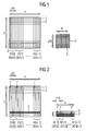
- Fig. 1 gives a basic illustration of an inventive RAM circuit based on the inventive external bitline-related repair approach.
- the memory cells 2 of a memory array 1 within a RAM circuit are arranged into y (e.g. 512) rows and x (e.g. 512) columns; the memory array 1 comprises a number of x ⁇ y memory cells 2.
- a plurality of x memory cells 2 within one row are assigned to one wordline (not shown), whereas a plurality of y memory cells 2 within one column are assigned to one bitline (not shown).
- n n-bit-wide input and output
- To each input or output port a plurality of x/n bitlines is assigned.
- the selection of one bitline for each plurality of x/n bitlines is carried out by column multiplexers (not shown).
- a substitution memory 4 which comprises at least y memory cells.
- a memory array 4 of 8-(y/8) memory cells 3' is used for the substitution of y memory cells within a particular bitline-related set 3 of memory cells 2.
- substitution memory array 4 is external to the main memory array 1, i.e. the substitution memory array 4 is placed outside the main memory array 1.
- the substitution memory array 4 Since during a random word-wise read or write access of the main memory array 1 only one port DI [0], DI [1], .., DI [n-1] or DO [0], DO [1], .., DO[n-1] is affected by the memory substitution, the substitution memory array 4 is accessed via an 1-bit-wide input or output. The signal on the 1-bit-wide input or output substitutes the signal on the affected port DI [0], DI [1], .., DI [n-1] or DO [0], DO [1], .., DO [n - 1] .
- bitline-related repair approach which means that not only one particular bitline-related set 3 of memory cells 2 but all x/n (here: 4) bitline-related sets of memory cells 2 which are assigned to one port DI[i] or DO[i] (e.g. DI [0], DO [0]) are substituted, the number of memory cells within the substitution memory array 4 has to be increased to y. (x/n) .
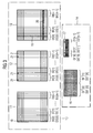
- FIG. 2 shows a basic illustration of an inventive RAM circuit based on the inventive external wordline-related repair approach in combination with the word-related repair approach.
- Figurative elements of Fig. 1 and Fig. 2 which are related to the same reference signs are basically same.
- substitution memory array 6 which comprises at least x memory cells.
- the substitution memory array 6 is external to the main memory array 1.
- the number x of memory cells per row in the main memory array 1 and the number x' of memory cells per row in the substitution memory array 6 may be different.
- the ratio x/x' is an integer.
- the number x' is half the number x. Therefore, in Fig. 2 two rows within the substitution memory array 6 are used for the substitution of one row within the main memory array 1.
- word-related sets 7 of memory cells 2 and not solely complete wordline-related sets of memory cells 2 can be substituted by memory cells 7' within the substitution memory array 6.
- FIG. 3 shows a basic illustration of an inventive RAM circuit with multiple main memory arrays based on multiple repair approaches.
- a main memory block 10 comprises a plurality (here: 3) of memory arrays 11, 12, 13. To each input port DI[0], DI [1], .., DI [n-1] or output port DO [0], DO [1], .., DO [n-1] of the main memory block 10 a number of x/n bitlines per memory array 11, 12, 13 is assigned.
- the RAM circuit also comprises a substitution memory 14 which contains two memory blocks 16 and 17.
- the bitline-related memory block 16 is provided for the substitution of a first 18 and a second 19 bitline-related set of memory cells. Since the memory block 16 is capable to substitute two bitline-related sets of memory cells, the memory block 16 comprises for the data input and the data output each two ports DI'' [0], DI'' [1] and DO"[0], DO" [1], respectively.
- a wordline/word-related memory array 17 is provided for the substitution of a wordline-related set 20 of memory cells and for the substitution of a word-related set 21 of memory cells according to the explanations regarding Fig. 2.
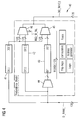
- Fig. 4 shows a simplified block diagram of an implemented inventive RAM circuit 40, which is an embedded SRAM circuit.
- the RAM circuit supports a wordline-related, a word-related and a bitline-related repair approach.
- the RAM circuit 40 comprises a main memory block 41, a wordline/word-related substitution memory block 42 for wordline/word-related substitution of defective memory cells within the main memory block 41 and a bitline-related substitution memory block 43 for bitline-related substitution of defective memory cells within the main memory block 41.
- the indication "[]" denotes that the particular signal, input or output comprises several bits.
- bitline-related memory substitution two multiplexers 44 and 45 are provided.
- the 128-to-1 multiplexer 44 selects one affected bitline of the 128 bitlines of the input DI_RAM[] in case an addressed memory cell within the main memory block 41 is substituted.
- the output signal of the multiplexer 44 is fed to the data input DI '' of the bitline-related substitution memory block 43.
- the 129-to-128 multiplexer 45 (implemented by a plurality of 128 2-to-1 multiplexers) is used to deselect one bitline of the 128 bitlines of the data output DO[] of the main memory block and to substitute the deselected bitline with the data output DO'' of the bitline-related substitution memory block 43 in case an addressed memory cell within the main memory block 41 is substituted.
- the output of the multiplexer is connected to the data output DO_RAM[] of the RAM circuit.
- Both multiplexers 44 and 45 are controlled via an 128-bit-wide select signal MUXD[]. Only the bit of the signal MUXD[] which corresponds to a substituted bit of the signal DI_RAM[] or DO_RAM [] is high, whereas the remaining 127 bits are low.
- a 256-to-128 multiplexer 46 (implemented by a plurality of 128 2-to-1 multiplexers) is provided. During read access the multiplexer 46 selects either the 128-bit-wide signal at the output DO[] of the main memory block 41 or the 128-bit-wide signal at the output DO'[] of the wordline/word-related substitution memory block 42 and feeds the selected signal to the output DO_RAM[] of the RAM circuit 40.
- the multiplexer 46 is controlled by an 1-bit-wide select signal RED_W_WL.
- no particular multiplexer is necessary because the wordline/word-related substitution memory block 42 is disabled in case the current address is not affected by wordline/word-related memory substitution.
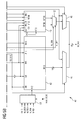
- Fig. 5 shows a detailed block diagram of the implemented inventive RAM circuit according to Fig. 4.
- Figurative elements of Fig. 4 and Fig. 5 which are related to the same reference signs are basically same.
- Circuit elements which are exclusively assigned to wordline-related and word-related memory substitution are marked by dotted areas. In case these circuit elements are omitted the RAM circuit does not support wordline/word-related memory substitution but only bitline-related memory substitution.
- the main memory block 41 comprises multiple memory arrays similar to the main memory block 12 according to Fig. 3.
- the main memory block 41 contains 8 memory arrays, with a particular memory array being addressed by a 3-bit-wide address signal component Az[] of the address signal A[].
- a particular wordline is selected by a 9-bit-wide address signal component Ax[].
- a plurality of 4 bitlines per memory array is assigned to each port of the data input DI[] or data output DO[], i.e. each column multiplexer is connected to 4 bitlines.
- One particular bitline out of the 4 bitlines is selected by a 2-bit-wide address signal component Ay[].
- the operation mode i.e. read or write access
- the system clock is provided by the signal CLK.
- the main memory block is enabled by the chip-select signal CSB.
- Table 1 provides the truth table of the main memory block 41.
- Table 1 CLK CSB RWB WIB [i] A [i] DI [i] DO [i] read low->high low high low/high address low/high data out write low->high low low low address data in old data out disabled low->high high low/high low/high low/high low/high old data out
- the main memory block supports writing of individual bits via a low-active 128-bit-wide signal WIB_RAM[] (write individual bar), i.e. the write operation for each bit of an addressed word can be individually enabled or disabled.
- WIB_RAM[i] of the signal WIB_RAM[] is high, the corresponding bit of the data input DI[i] is not written in the memory.
- the information of the signal WIB_RAM[] is also considered in case one of the substitution memory blocks 42 or 43 is accessed. Before feeding the signal WIB_RAM[] to the substitution memory block 42 or 43, the signal WIB_RAM[] is sampled via the parallel flip-flops 59.
- the sampled version of the signal WIB_RAM[] is fed to the input WIB[] of the substitution memory block 42.
- an 128-to-1 multiplexer 60 is provided which selects in dependency of the signal MUXD[] that particular bit of the sampled version of the signal WIB_RAM[] which corresponds to the substituted bit of the signal DI_RAM[].
- the RAM circuit 40 is capable to substitute 2 word-related sets, 2 wordline-related sets and 2 bitline-related sets of memory cells within the main memory block 41.
- address information of the substituted memory cells is stored (after memory test) within memory elements (not shown), particularly non-volatile memory elements.
- the stored address information is compared with address information which is derived from the address signal A[].
- the wordline-related memory repair for specifying the two substituted wordline-related sets of memory cells two 12-bit-wide codes FWL0[] and FWL1[] are employed; the codes FWL0[] and FWL1[] each specify the particular memory array (which corresponds to Az[]) and the particular wordline (which corresponds to Ax[]). The codes FWL0[] and FWL1[] are compared with the components Az[] and Ax[] of the current address signal A [] .
- bitline-related memory repair for specifying the two substituted bitline-related sets of memory cells two 5-bit-wide codes FBL0[] and FBL1[] amongst other information are employed.
- the codes FBL0[] and FBL1[] each specify the particular memory array (which corresponds to Az[]) and one bitline-related set of memory cells out of 4 bitline-related sets of memory cells for each port of the data input DI[] or data output DO[] (which corresponds to Ay[]).
- the codes FBL0[] and FBL1[] are compared with the components Az[] and Ay[] of the current address signal A[].
- 1-bit-wide enable signals FBL0_EN FBL1_EN, FW0_EN, FW1_EN, FWL0_EN and FWL1_EN are provided which indicate whether the corresponding redundancy memory resource is used or not.
- the enable signals FBL0_EN and FBL1_EN indicate whether a first and a second bitline-related set of memory cells are substituted or not.
- the enable signals FW0_EN and FW1_EN indicate whether a first and a second word-related set of memory cells are substituted or not.
- the enable signals FWL0_EN and FWL1_EN indicate whether a first and a second wordline-related set of memory cells are substituted or not.
- the signals FBL0_EN, FBL1_EN, FW0_EN, FW1_EN, FWL0_EN and FWL1_EN are read out of memory elements (not shown), particularly non-volatile memory elements.
- the flip-flop FF1 generates an activation pulse within the signal ACTCOMP (ACTCOMP is active high) that controls the operation of the address comparators 47, 48 and 49 and the comparator flip-flops 51.
- the flip-flop FF2 generates an activation pulse within the signal ACT (ACT is active high) that controls the operation of the flip-flop RWBFF, the address flip-flops 50, the data input flip-flops 56 and the flip-flops 59 at the input WIB_RAM[].
- the flip-flop RWBFF, the address flip-flops 50, the data input flip-flops 56 and the flip-flops 59 at the input WIB_RAM[] are used to sample the signals RWB, A[], DI[] and WIB[], respectively, at the rising edge of the clock signal. Thus, the sampled values of these signals are stored during the following clock cycle.
- the two bitline-related address comparators 47 compare the stored codes FBL0 [] and FBL1 [] with sampled versions QAz [] and QAy[] of the components Az[] and Ay[] of the current address signal A[].
- the sampled versions QAz[], QAx[] and QAy[] of the address components Az [], Ax[] and Ay[] are generated by a plurality of flip-flops 50.
- Each of the two comparisons is performed in case the corresponding enable signal FBL0_EN or FBL1_EN, respectively, is set to high.
- the two word-related address comparators 48 compare the stored codes FW0[] and FW1[] with the sampled versions QAz[], Qax[], QAy [] of the components Az[], Ax[] and Ay[] of the current address signal A[]. Each of the two comparisons is performed in case the corresponding enable signal FW0_EN or FW1_EN, respectively, is set to high.
- the two wordline-related address comparators 49 compare the stored codes FWL0[] and FWL1[] with the sampled versions QAz[] and Qax[] of the components Az[] and Ax[] of the current address signal A[]. Each of the two comparisons is performed in case the corresponding enable signal FWL0_EN or FWL1_EN, respectively, is set to high.
- the output signals of the comparators 47, 48 and 49 are sampled by a plurality of parallel flip-flops 51.
- the first and second output signal BL_RED0 and BL_RED1 of the flip-flops 51 which are active high, control the activation of the first and second bitline-related memory substitution.
- the third and fourth output signal W_RED0 and W_RED1 (active high) of the flip-flops 51 control the activation of the first and second word-related memory substitution.
- the fifth and sixth output signal WL_RED0 and WL_RED1 (active high) of the flip-flops 51 control the activation of the first and second wordline-related memory substitution.
- bitline-related signals BL_RED0 and BL_RED1 are fed to a NOR-gate 52, the output signal RED_BL (active low) of which indicates whether at least one bitline-related set of memory cells is substituted or not.
- the word-related signals W_RED0 and W-RED1 and wordline-related signals WL_RED0 and WL_RED1 are fed to a NOR-gate 53 with 4 inputs, the output signal RED_W_WL (active low) of which indicates whether at least one wordline-related or word-related set of memory cells is substituted or not.
- bitline-related substitution memory block 43 is enabled via its input CSB (chip-select bar).
- the corresponding 7-bit-wide code FIO0[] or FI01[] of the first or the second bitline-related set of memory cells is selected by a multiplexer 54.
- the selected code FIO[] is decoded via a decoder 55 to the above-mentioned 128-bit-wide signal MUXD[], with the bit-width of the signal MUXD[] corresponding to the number of ports of the data input/output of the RAM circuit.
- the signal MUXD[] controls the multiplexers 44 and 45 for write and read memory access, respectively.
- the selected bit is first of all fed to both input ports DI" [0] and DI" [1] of the bitline-related substitution memory block 43, with each input port DI" [0] and DI” [1] being dedicated to one bitline-related set of memory cells to substitute (similar to memory block 16 in Fig. 3).
- the selection whether the first input port DI" [0] or the second input port DI" [1] is actually used is controlled via the state of the inputs WIB[0] and WIB[1], which work analogously to the input WIB[] of the main memory 41.
- WIB[0] or WIB[1] the data signal at the output of the multiplexer 44 is written into the corresponding memory cells within the memory block 43.
- the state of the inputs WIB[0] and WIB[1] is controlled via the OR-gates 61, 62 in dependency of the signals BL_RED0 and BL_RED1, respectively, and also in dependency of the output signal of the multiplexer 60.
- one of the two data output ports DO'' [0] and DO''[1] is selected via the 2-to-1 multiplexer 57, with each output port DO" [0] and DO" [1] being dedicated to one substituted bitline-related set of memory cells.
- the selection of the multiplexer 57 is controlled by the signals BL_RED0 and BL_RED1: in case BL_RED0 is high, the port DO " [0] is selected; in case BL_RED1 is high, the port DO" [1] is selected.
- the 129-to-128 multiplexer 45 which drives the global data output bus DO_RAM[], deselects one bitline of the 128 bitlines of the data output DO[] of the main memory block 41 and substitutes the signal on the deselected bitline with the signal on the data output of the multiplexer 57.
- the number of addresses of the memory block 43 is equal to the number y of memory cells within one bitline-related set of memory cells of the main memory block 41.
- y 512 memory cells are connected to one bitline; consequently, the memory block 43 has 512 addresses.
- the address input A2[] of the memory block 43 is driven by the sampled version QAx[] of the address component Ax[] which specifies the current wordline and has 512 different values.
- the word/wordline-related substitution memory block 42 is enabled via its input CSB (chip-select bar).
- the word/wordline-related substitution memory block 42 offers the same number of ports at the data input DI'[] and the data output DO' [] than the main memory block 41.
- the number of addresses of the word/wordline-related substitution memory block 42 is reduced compared to the number of addresses of the main memory block 41.
- the main memory block 41 and the word/wordline-related substitution memory block 42 may have a different number x/n of bitlines which are assigned to one column multiplexer (e.g. 4 bitlines in memory block 41 and 2 bitlines in memory block 42).
- an address generator 58 is employed which generates an appropriate address signal for driving the address input A1[] of the memory block 42.
- the address generator 58 can be also regarded as an address converter which modifies a particular main memory address signal A[] or a subset thereof to an appropriate address signal for driving the address input A1[] of the memory block 42.
- the address generator 58 is controlled by the sampled version QAy[] of the address component Ay[] and the signals W_RED0, W_RED1, WL_RED0 and WL_RED1.
- the address generator 58 is configurable, i.e. it supports different designs of the main memory block 41 with different widths x/n of the column multiplexers in the main memory block 41. The actual width x/n is configured by the signal MUX_CODE.
- the data at the output DO'[] of the memory block 42 is selected via the multiplexer 46 and fed to the global data output bus DO_RAM[] .
- the RAM circuit 40 has to be modified in the following way:
- the particular choice of the parameters of the inventive RAM circuit 40 e.g. the number x of bitlines (here 512), the number y of wordlines (here 512), the number n of I/O-ports (here 128) or the number of memory arrays within the main memory block 41 (here 8), is arbitrary.
- the inventive RAM circuit 40 can also be implemented with a different choice of such parameters.
- the RAM circuit 40 merely supports memory substitution of one single independent main memory block 41
- the invention is not limited to memory substitution of a single independent main memory block.
- these main memory blocks share the resources for memory substitution, in particular the substitution memory blocks.
- the access to the substitution memory blocks is preferably redirected according to the particular main memory block which uses the substitution memory blocks for a given clock cycle.
- a set of redirections means is provided which redirects the address information, the signal RWB, the data input and the data output between the substitution memory blocks and the different main memory blocks.
- the invention is not limited to main memory blocks with one data input and one data output. It is included within the scope of the invention to employ main memory blocks with several data inputs and several data inputs. In this case, the substitution memory blocks preferably have the same number of data inputs and data outputs as the main memory block. In addition, specific redirection means for the various data inputs and data outputs are provided.
- the inventive idea is not strictly limited to the substitution of a complete bitline-related, port-related or wordline-related set of memory cells. It is conceivable that the substitution memory block is arranged to substitute a part of a bitline-related, port-related or wordline-related set of memory cells, e.g. one fourth of a bitline-related set of memory cells.
Abstract

Description
- The invention relates to memory circuits, particularly to RAM (random access memory) circuits, with memory redundancy for the substitution of defect memory cells.
- RAM circuits comprise one or more two-dimensional arrays of 1-bit-memory cells. In DRAM (dynamic random access memory) circuits the information storage in a memory cell is based on the charge state of a capacitor, whereas in SRAM (static random access memory) circuits flip-flops with positive feedback for information storage are employed.
- The memory cells of one array are arranged into y rows and x columns. The memory cells of one row are assigned to one wordline, whereas the memory cells of one column are assigned to one bitline. The memory cells are selected via the signals on the wordlines; for the actual data access, i.e. reading and writing of the data, the bitlines are employed.
- Generally, RAM circuits are accessed word-oriented via an appropriate address signal, i.e. each code of the address signal is assigned to a specific number of n memory cells within one memory array which are read out or written in parallel. The n-bit-wide information is equivalent to one word. Consequently, such RAM circuits comprise n-bit-wide inputs and outputs with n ports. In this case, to each port of the n ports a plurality of x/n bitlines is assigned, with one bitline per port being selectable via port-related column multiplexers.
- For word-oriented memory access a multi-bit-wide address signal is applied to the RAM circuit, which generally exhibits three code components. A first code component, typically ld(y)-bit-wide, specifies the wordline of the accessed memory cells. A second code component, typically ld(x/n)-bit-wide, specifies one bitline for each plurality of x/n grouped bitlines. The optional third code component specifies the index of the memory array in case more than one memory array is employed.
- RAM circuits may contain one or more randomly distributed defective memory cells after fabrication. Without appropriate countermeasures such RAM circuits with defect memory cells would be unusable for most applications even if only a small number of memory cells compared to the total number is affected. Generally, the larger the number of memory cells within one memory array, the lower the probability that the array is fault-free.
- To prevent most RAM memories from being discarded once one or more defect memory cells are located during memory test, substitution memory cells are provided which allow a substitution of such defective memory cells within the main memory. Normally, the address codes or subsets thereof of the substituted memory cells are stored in non-volatile memory cells, which are generally implemented by fuses. If a memory cell is accessed the stored address information is compared with the actual address information of the address signal. In case of a positive comparison result the access is redirected to the substitution memory cells.
- For the substitution of defect memory cells different approaches are conceivable:
- 1. Bitline-related repair approach
According to the so called bitline-related repair approach a complete bitline-related set of y memory cells being connected to the same bitline in one memory array is substituted with y substitution memory cells. In case a substituted bitline-related set comprises y = 512 memory cells, all 512 memory cells are substituted. - 2. Wordline-related repair approach
In case a wordline-related repair approach is employed, a complete wordline-related set of x memory cells being connected to the same wordline in one memory array is substituted by the same number of substitution memory cells. Similar to the bitline-related repair approach all memory cells connected to one wordline (e.g. 512 memory cells) are substituted. - 3. Word-related repair approach
By applying a word-related repair approach, a word-related set of n memory cells which are addressed by one single address code is substituted by the same number of substitution memory cells. - 4. Port-related or I/O-related repair approach
The port-related repair approach (also called I/O repair) is an extension of the bitline-related repair approach, i.e. more than one bitline is substituted. According to a port-related repair approach those x/n.y memory cells which are connected to a plurality of x/n bitlines, with the x/n bitlines being assigned to one port, i.e. connected to one column multiplexer, are substituted by the same number of substitution memory cells. - Generally, the bitline-related repair approach and the wordline-related repair approach are alternatively employed.
- Regarding the implementation of the bitline-related repair approach or alternatively the wordline-related repair approach additional bitlines or additional wordlines, respectively, which are connected to substitution memory cells are provided. Thus, the main memory and the substitution memory form a common array of main memory cells and substitution memory cells.
- Consequently, the memory cells of the main memory and the substitution memory are typically identical. Thus, process failures affecting the yield of the memory cells of the main memory affect the yield of the substitution memory cells in the same way.
- A further drawback of such an implementation of the bitline-related repair approach or alternatively the wordline-related repair is that the memory access time of the RAM circuit is increased in comparison to the memory access time of a RAM circuit without bitline- or wordline-related substitution memory. This is due to the fact that earlier to the actual memory access the above-mentioned comparison regarding stored address information is performed.
- In case the RAM circuit comprises more than one memory array, additional bitlines or wordlines which are connected to substitution memory cells, appropriate comparators and fuses for non-volatile address information storage are needed for each memory array. This leads to a huge area overhead.
- In addition, the concrete implementation of the bitline- or wordline-related repair approach is only valid for a particular implementation of the main memory.
- The document US 6,484,271 B1 describes a memory system with redundancy for the substitution of defective memory cells within a main memory. The main memory comprises a plurality of memory instances. An extra substitution or redundant memory is provided which substitutes defective memory cells within the main memory, with the substitution memory being capable to substitute word-related sets of memory cells. The substitution memory is not capable to substitute complete wordline-related sets of memory cells or bitline-related sets of memory cells.
- In the document US 5,644,541 a memory system with redundancy for the substitution of defective memory cells within a plurality of DRAM memory circuits is presented. Similar to the document US 6,484,271 B1 an extra substitution memory is provided, which substitutes defective memory cells within the plurality of DRAM memory circuits. The substitution memory substitutes single defective memory cells within the plurality of DRAM memory circuits. Complete wordline-related or bitline-related sets of memory cells within the plurality of DRAM memory circuits are not substituted.
- It is an object of the present invention to provide a memory circuit, particularly a RAM circuit, with memory redundancy for bitline- or wordline-related substitution of defect memory cells which overcomes the above-mentioned drawbacks.
- The above-mentioned object of the present invention is achieved by a memory circuit according to
claim 1 or claim 20. - The inventive memory (e.g. RAM) circuit for read and write access according to
claim 1 comprises a main memory block, which comprises at least one complete memory array of memory cells. The memory cells are connected to wordlines as well as bitlines and are addressable via an address signal. - In addition, the memory circuit comprises a substitution memory block with at least one data input and at least one data output for the substitution of memory cells within the main memory block. The substitution memory block comprises a plurality of substitution memory cells. A substantial feature of the present inventive memory circuit is that the substitution memory block is external to the main memory block, i.e. the substitution memory block is spatially separated from the main memory block. Thus, the substitution memory cells and the memory cells of the main memory block do not form a memory array. In case the substitution memory block comprises at least one complete memory array of memory cells being connected to wordlines and bitlines, the bitlines within the main memory and within the substitution memory block are distinct nets. Also the wordlines within the main memory and within the substitution memory block are distinct nets.
- The substitution memory block is arranged to substitute at least one bitline-related set of memory cells being connected to the same bitline in one memory array. Thus, a bitline-related repair approach, as mentioned above, is employed.
- Furthermore, the inventive memory circuit comprises redirection means for redirecting the access to a memory cell of the at least one respective substituted bitline-related set of memory cells in the main memory block to the substitution memory block.
- The inventive external bitline-related repair approach provides the advantage that the physical implementation of the substitution memory block is not bound to the physical implementation of the main memory block. Advantageously, the substitution memory cells within the substitution memory block are less dense packed compared to the memory cells within the main memory block.
- A further advantage of the memory circuit according to
claim 1 is that the processing speed of the circuit is generally not affected by the memory redundancy since the comparison can be performed in parallel to the main memory access. - In addition, the inventive solution provides the option that the substitution memory block can be shared for the substitution of several memory arrays within the main memory block.
- Thus, the total area overhead due to memory redundancy is reduced.
- Furthermore, the external substitution memory is not bound to one specific main memory block and thus can be flexibly used for different designs of the main memory block.
- In addition, the number of non-volatile memory cells for the address information storage is not dependent on the total number of memory array within the main memory.
- It should be noted that the inventive memory circuit is not limited to a RAM circuit; the scope of the invention also comprises other types of memory circuits with read/write functionality, e.g. flash-memory circuits. Theoretically, the inventive memory circuit could be even a read-only memory circuit, i.e. without data inputs.
- Advantageously, the redirection means comprise a first multiplexer for write access. The input of the first multiplexer is electrically connected to receive the signal on the data input of the memory circuit and the output of the first multiplexer is electrically connected to the data input of the substitution memory block.
- According to a preferred embodiment, the redirection means comprise a second multiplexer for read access. The input of the second multiplexer is electrically connected to receive the signal on the data output of the substitution memory block and the signal on the data output of the main memory block. The output of the second multiplexer is electrically connected to the data output of the memory circuit.
- It should be noted that the presence of the second multiplexer does not necessarily imply that the redirection means comprise the first multiplexer.
- Advantageously, the data input and the data output of the memory circuit as well as the data input and the data output of the main memory block are each n-bit-wide. Thus, these data inputs and data outputs each comprise n ports, with n > 1.
- As mentioned above the n-bit-wide information at the data inputs or data outputs is equivalent to one word.
- According to a preferred embodiment, the at least one data input and the at least one data output of the substitution memory block are each 1-bit-wide.
- It should be noted that the substitution memory block may comprise not only one data input and one data output but more than one data input and data output (which is equivalent to a multi-bit-wide input or output). Nevertheless such memory block comprises still at least one 1-bit-wide data input and at least one 1-bit-wide data output.
- In case the data input of the memory circuit and the main memory block are each n-bit-wide and the at least one data input of the substitution memory block is 1-bit-wide, the first multiplexer is an n-to-1-multiplexer, i.e. with n binary input signals and 1 binary output signal, and the second multiplexer is an (n+1) -to-n-multiplexer, i.e. with n+1 binary input signals and n binary output signals.
- For write access, the first multiplexer selects one port of the n-bit-wide data input of the memory circuit, with the selected port being related to a currently addressed defective memory cell. The selected port is connected to the at least one 1-bit-wide data input of the substitution memory block via the first multiplexer, thereby writing the data which is dedicated to the defective memory cell into the substitution memory block.
- For read access, the second multiplexer replaces the signal of one port of the n-bit-wide data output of the main memory block with the signal of one 1-bit-wide data output of the substitution memory block. This particular port is related to a currently addressed defective memory cell. The signals on the other ports of the data output of the main memory block are fed-through to the output of the memory circuit.
- Advantageously, the redirection means comprise memory means, particularly fuses, for storing at least one first code specifying the at least one respective substituted bitline-related set of memory cells. In this case the redirection means further comprise a first comparator, which compares the at least one stored first code (related to a substituted bitline-related set of memory cells) with a code being derived from the current address signal. Therefore, the first comparator checks if the current address of the address signal is related to a substituted memory cell.
- In this case, the substitution memory block advantageously comprises a particular input (called chip-select input) which enables the substitution memory block. The chip-select input is driven by the output of the first comparator. Optionally, logic gates are placed between the output of the first comparator and the chip-select input.
- If the at least one stored first code is equal to the code which is derived from the current address signal, the substitution memory block is enabled via the chip-select input. Otherwise the substitution memory block is disabled.
- Advantageously, within each memory array, to each port of the data input and/or data output of the main memory block a plurality of bitline-related sets of memory cells is assigned. Particularly, to each port of the n ports a plurality of x/n bitline-related sets of memory cells (if x is the number of bitlines of one memory array) is assigned. The at least one first code specifies one bitline-related set of memory cells within each plurality of bitline-related sets of memory cells. In this case, the first code is advantageously ld(x/n)-bit-wide.
- According to a preferred embodiment, the main memory block comprises a plurality of complete memory arrays. In this case, the substitution memory block can be shared for the substitution of defective memory cells within several memory arrays.
- If the main memory block comprises a plurality of memory arrays, the at least first code advantageously specifies the particular memory array, wherein the at least one respective substituted bitline-related set of memory cells is located.
- According to a preferred embodiment, the redirection means comprise memory means, typically fuses, for storing a second code. The second code specifies the port-index of any above-specified n-bit-wide data input and/or output which is related to the at least one respective substituted bitline-related set of memory cells. Particularly, the second code is ld(n)-bit-wide.
- In case such second code is provided, the redirection means advantageously comprise a decoder for decoding the second code to a select signal which controls any above-specified multiplexer. Since the two multiplexers select one port out of n ports (first multiplexer) or n ports out of n+1 ports (second multiplexer), the select signal is advantageously an n-bit-wide signal, with only the signal port corresponding to the substituted bitline-related set of memory cells being active.
- Advantageously, the substitution memory block is arranged to substitute not only one bitline-related set of memory cells but a plurality m of bitline-related sets of memory cells; particularly, the substitution memory block comprises m 1-bit-wide data inputs and m 1-bit-wide data outputs. In this case, the memory means for storing the first code are arranged to store m first codes of m substituted bitline-related sets of memory cells.
- Advantageously, the redirection means comprise m first comparators, which compare the m stored first codes with a code being derived from the current address signal. Alternatively, the redirection means comprise one comparator, which is comparing each first stored code one after the other with a code being derived from the current address signal. Additionally, memory means for storing a plurality of m second codes are to be provided.
- According to a preferred embodiment, the substitution memory block is arranged to substitute not only one bitline-related set but at least one port-related set of memory cells within one memory array. The at least one port-related set of memory cells comprises those bitline-related sets of memory cells within one memory array which are assigned to the same port of the data input and data output of the main memory block. The redirection means are arranged to redirect the access to a memory cell of the at least one substituted port-related set of memory cells to the substitution memory block.
- Thus, the substitution memory block and the redirection means support the above-mentioned port-related repair (I/O repair) approach. The above-mentioned advantages of the inventive external bitline-related repair approach are also valid for the inventive external port-related repair approach.
- In case a port-related repair approach is employed, the redirection means advantageously comprise memory means for storing at least one third (which does not necessarily imply the presence of a first and second code) code which specifies the at least one respective substituted port-related set of memory cells. Furthermore, the redirection means comprise a second (which does not necessarily imply the presence of a first comparator) comparator which compares the at least one stored third code with a code being derived from the address signal.
- The third code and the second comparator correspond to the above-mentioned first code and first comparator, respectively, of the bitline-related approach.
- Further preferred embodiments of the port-related repair approach which are analogous to the above-mentioned preferred embodiments of the bitline-related repair approach are described in the
dependent claims 16 to 18. - With respect to a second aspect of the invention, the inventive memory (e.g. RAM) circuit according to
claim 20 employs a wordline-related repair approach. - The memory circuit comprises a main memory block, which comprises at least one complete memory array of memory cells connected to wordlines and bitlines. The memory cells are addressable via an address signal.
- In addition, the memory circuit comprises a substitution memory block for the substitution of memory cells within the main memory block. The substitution memory block comprises a plurality of substitution memory cells. A substantial feature of the present inventive memory circuit is that the substitution memory block is external to the main memory block, i.e. the substitution memory block is spatially separated from the main memory block. Thus, the substitution memory cells and the memory cells of the main memory block do not form a memory array. The substitution memory block is arranged to substitute at least one wordline-related set of memory cells being connected to the same wordline in the at least one memory array. Thus, a wordline-related repair approach, as mentioned above, is employed.
- Furthermore, the inventive memory circuit comprises redirection means for redirecting the access to a memory cell of the at least one respective substituted wordline-related set of memory cells in the main memory block to the substitution memory block.
- The above-mentioned advantages of the memory circuit according to the inventive external bitline-related repair approach are also valid for the memory circuit according to the inventive external wordline-related repair approach.
- Also with respect to the second aspect of the invention, it should be noted that the inventive memory circuit is not limited to a RAM circuit; the scope of the invention also comprises other types of memory circuits with read/write functionality, e.g. flash-memory circuits. Theoretically, the inventive memory circuit could be even a read-only memory circuit, i.e. without data inputs.
- According to a preferred embodiment of the second aspect of the invention, the redirection means comprise a multiplexer for read access. The multiplexer is used to select either the signal on the output of the main memory block or the signal on the substitution memory block. The input of the multiplexer is electrically connected to receive the signal on the data output of the substitution memory block and the signal on the data output of the main memory block. The output of the multiplexer is electrically connected to the data output of the memory circuit.
- Advantageously, the data input and the data output of the memory circuit, the data input and the data output of the main memory block as well as the data input and the data output of the substitution memory are each n-bit-wide. Thus, these data inputs and data outputs each comprise n ports, with n > 1.
- As mentioned above the n-bit-wide information at the data inputs or data outputs is equivalent to one word.
- In case the data outputs of the memory circuit, the main memory block and the substitution memory block are each n-bit-wide, the multiplexer is advantageously implemented as a 2n-to-n-multiplexer, which either selects the signal on the data output of the main memory block or the substitution memory block.
- Advantageously, the redirection means comprise memory means for storing at least one code specifying the at least one respective substituted wordline-related set of memory cells, i.e. more than one code is conceivable to specify more than one wordline-related set of memory cells. In this case, the redirection means further comprise a first comparator, which compares the at least one stored code with a code which is derived from the current address signal.
- Thus, the first comparator checks if the current code of the address signal is related to a substituted memory cell.
- In this case, the substitution memory block advantageously comprises a chip-select input which enables the substitution memory block. The chip-select input is driven by the output of the first comparator. Optionally, logic gates are placed between the output of the first comparator and the chip-select input.
- If the at least one stored code is equal to the code which is derived from the current address signal, the substitution memory block is enabled via the chip-select input. Otherwise the substitution memory block is disabled.
- Since the substitution memory block comprises the chip-select input no particular multiplexer at the data input of the memory circuit for selecting either the data input of the main memory block or the data input of the substitution memory block is necessary. Only in case that the stored code is equal to the code which is derived from the current address signal, the data at the input of the memory circuit is written to the enabled substitution memory block.
- According to a preferred embodiment, the redirection means comprise an address generator. The address generator drives an address input of the substitution memory block. It further receives a code which is derived from the current address signal.
- Because the substitution memory block has a substantially smaller memory capacity than the main memory block, the addressing of the substitution memory block and the main memory block is completely different, i.e. the number of addresses of the substitution memory block is significantly smaller than the number of addresses of the main memory block. The address generator, which can be also regarded as an address converter, receives the current address signal or a subset of the current address signal of the memory circuit to generate an appropriate address signal for the substitution memory block.
- In case an address generator is provided, the address generator is advantageously configurable with respect to the structure of the main memory block, e.g. with respect to the total number of bitlines within one memory array of the main memory block which are related to one port of the main memory block. By providing a configurable address generator the external substitution memory is not bound to a specific main memory block and thus can be flexibly used for different designs of the main memory block.
- Advantageously, the address generator receives a configuration signal which specifies the total number of bitlines within one memory array of the main memory block which are related to one port of the main memory block.
- According to a preferred embodiment of the second aspect of the invention, the substitution memory block is arranged to substitute at least one word-related set of memory cells in the main memory. The word-related set of memory cells is addressed by one address code of the address signal. Thus, the inventive memory circuit further, i.e. beside the wordline-related repair approach, supports a word-related repair approach.
- Consequently, the redirection means are also arranged to redirect the access to a memory cell of the at least one respective substituted word-related set of memory cells in the main memory block to the substitution memory block.
- In case a word-related repair approach is supported, the redirection means advantageously comprise memory means for storing at least one address code of the at least one respective substituted word-related set of memory cells. The redirection means further comprise a second comparator, which compares the at least one stored address code with the code of the address signal.
- Regarding the first or alternatively the second aspect of the invention, the substitution memory cells within the substitution memory block are advantageously less dense packed compared to the memory cells within the main memory block, i.e. larger substitution memory cells in comparison to the memory cells of the main memory are used, resulting in an increased yield regarding the substitution memory block. Thus, the design rules of a semiconductor technology, which limit the physical dimensions on the lower end, can be followed within the substitution memory block. Layout waivers, which break these rules in favour of a denser layout and which are critical for the fabrication of the memory circuit, are not necessary for the substitution memory block. Furthermore, the increased physical dimensions of the substitution memory cells enable flexible usage of the substitution memory block for process technologies with smaller as well as larger feature sizes.
- It should be noted that the inventive memory circuit might also support a bitline-related or port-related repair approach according to the first aspect of the invention as well as a wordline-related (and optional also a word-related) repair approach according to the second aspect of the invention.
- The invention is explained below in an exemplary manner with reference to the drawings, in which
- Fig. 1
- shows a basic illustration of an inventive RAM circuit based on the inventive external bitline-related repair approach;
- Fig. 2
- shows a basic illustration of an inventive RAM circuit based on the inventive external wordline-related repair approach in combination with the word-related repair approach;
- Fig. 3
- shows a basic illustration of an inventive RAM circuit with multiple main memory arrays based on multiple repair approaches;
- Fig. 4
- shows a simplified block diagram of an implemented inventive RAM circuit; and
- Fig. 5
- shows a detailed block diagram of the implemented inventive RAM circuit.
- Fig. 1 gives a basic illustration of an inventive RAM circuit based on the inventive external bitline-related repair approach. The
memory cells 2 of amemory array 1 within a RAM circuit are arranged into y (e.g. 512) rows and x (e.g. 512) columns; thememory array 1 comprises a number of x·y memory cells 2. A plurality ofx memory cells 2 within one row are assigned to one wordline (not shown), whereas a plurality ofy memory cells 2 within one column are assigned to one bitline (not shown). - The
memory array 1 is word-wise accessed, i.e. it comprises an n-bit-wide input and output (e.g. n = 128) with n ports DI [0], DI [1], .. DI [n-1] and DO [0], DO [1], .. DO [n-1], respectively. To each input or output port a plurality of x/n bitlines is assigned. The selection of one bitline for each plurality of x/n bitlines is carried out by column multiplexers (not shown). - In case one or more memory cells within a particular bitline-related
set 3 ofmemory cells 2 are defective, the whole particular bitline-relatedset 3 ofmemory cells 2 is substituted by memory cells 3' within asubstitution memory 4, which comprises at least y memory cells. In Fig. 1 amemory array 4 of 8-(y/8) memory cells 3' is used for the substitution of y memory cells within a particular bitline-relatedset 3 ofmemory cells 2. - A substantial feature of the inventive RAM circuit is that the
substitution memory array 4 is external to themain memory array 1, i.e. thesubstitution memory array 4 is placed outside themain memory array 1. - Since during a random word-wise read or write access of the
main memory array 1 only one port DI [0], DI [1], .., DI [n-1] or DO [0], DO [1], .., DO[n-1] is affected by the memory substitution, thesubstitution memory array 4 is accessed via an 1-bit-wide input or output. The signal on the 1-bit-wide input or output substitutes the signal on the affected port DI [0], DI [1], .., DI [n-1] or DO [0], DO [1], .., DO [n - 1] . - For a port-related repair approach (not shown), which means that not only one particular bitline-related
set 3 ofmemory cells 2 but all x/n (here: 4) bitline-related sets ofmemory cells 2 which are assigned to one port DI[i] or DO[i] (e.g. DI [0], DO [0]) are substituted, the number of memory cells within thesubstitution memory array 4 has to be increased to y. (x/n) . - Fig. 2 shows a basic illustration of an inventive RAM circuit based on the inventive external wordline-related repair approach in combination with the word-related repair approach. Figurative elements of Fig. 1 and Fig. 2 which are related to the same reference signs are basically same.
- In case one or more memory cells within a particular wordline-related
set 5 ofmemory cells 2 are defective, the whole particular wordline-relatedset 5 ofmemory cells 2 is substituted by memory cells 5' within asubstitution memory array 6, which comprises at least x memory cells. Thesubstitution memory array 6 is external to themain memory array 1. Thesubstitution memory array 6 is accessed via an n-bit-wide input and output (e.g. n = 128) with n ports DI'[0], DI'[1], .., DI' [n-1] and DO' [0], DO' [1], ..,
DO' [n-1] . To each input port DI' [0], DI' [1], .., DI' [n-1] or output port DO' [0], DO'[1], .., DO'[n-1] a plurality of x'/n bitlines is assigned (x' = number of columns of the substitution memory array 6) - The number x of memory cells per row in the
main memory array 1 and the number x' of memory cells per row in thesubstitution memory array 6 may be different. Advantageously, the ratio x/x' is an integer. In Fig. 2 the number x' is half the number x. Therefore, in Fig. 2 two rows within thesubstitution memory array 6 are used for the substitution of one row within themain memory array 1. - In addition, also word-related
sets 7 ofmemory cells 2 and not solely complete wordline-related sets ofmemory cells 2 can be substituted by memory cells 7' within thesubstitution memory array 6. - Fig. 3 shows a basic illustration of an inventive RAM circuit with multiple main memory arrays based on multiple repair approaches. A
main memory block 10 comprises a plurality (here: 3) ofmemory arrays memory array - The RAM circuit also comprises a
substitution memory 14 which contains twomemory blocks 16 and 17. The bitline-relatedmemory block 16 is provided for the substitution of a first 18 and a second 19 bitline-related set of memory cells. Since thememory block 16 is capable to substitute two bitline-related sets of memory cells, thememory block 16 comprises for the data input and the data output each two ports DI'' [0], DI'' [1] and DO"[0], DO" [1], respectively. In addition, a wordline/word-related memory array 17 is provided for the substitution of a wordline-relatedset 20 of memory cells and for the substitution of a word-relatedset 21 of memory cells according to the explanations regarding Fig. 2. - Fig. 4 shows a simplified block diagram of an implemented
inventive RAM circuit 40, which is an embedded SRAM circuit. The RAM circuit supports a wordline-related, a word-related and a bitline-related repair approach. - The
RAM circuit 40 comprises amain memory block 41, a wordline/word-relatedsubstitution memory block 42 for wordline/word-related substitution of defective memory cells within themain memory block 41 and a bitline-relatedsubstitution memory block 43 for bitline-related substitution of defective memory cells within themain memory block 41. TheRAM circuit 40 has an 128-bit-wide data input DI_RAM[] and an 128-bit-wide data output DO_RAM[] (n = 128). The indication "[]" denotes that the particular signal, input or output comprises several bits. - Depending on the address signal (not shown), data has to be read or written in the
main memory block 41 or in the substitution memory blocks 42 or 43. For the control of the data flow a plurality of multiplexers is employed. - For the data flow regarding the bitline-related memory substitution two
multiplexers multiplexer 44 selects one affected bitline of the 128 bitlines of the input DI_RAM[] in case an addressed memory cell within themain memory block 41 is substituted. The output signal of themultiplexer 44 is fed to the data input DI '' of the bitline-relatedsubstitution memory block 43. During read access the 129-to-128 multiplexer 45 (implemented by a plurality of 128 2-to-1 multiplexers) is used to deselect one bitline of the 128 bitlines of the data output DO[] of the main memory block and to substitute the deselected bitline with the data output DO'' of the bitline-relatedsubstitution memory block 43 in case an addressed memory cell within themain memory block 41 is substituted. The output of the multiplexer is connected to the data output DO_RAM[] of the RAM circuit. Bothmultiplexers - For the data flow regarding the wordline- or word-related memory substitution a 256-to-128 multiplexer 46 (implemented by a plurality of 128 2-to-1 multiplexers) is provided. During read access the
multiplexer 46 selects either the 128-bit-wide signal at the output DO[] of themain memory block 41 or the 128-bit-wide signal at the output DO'[] of the wordline/word-relatedsubstitution memory block 42 and feeds the selected signal to the output DO_RAM[] of theRAM circuit 40. Themultiplexer 46 is controlled by an 1-bit-wide select signal RED_W_WL. For the data input, i.e. the write access, no particular multiplexer is necessary because the wordline/word-relatedsubstitution memory block 42 is disabled in case the current address is not affected by wordline/word-related memory substitution. - In addition, a plurality of flip-flops, several comparators, several fuses, an address generator and additional logic gates are provided for memory substitution, the functions of which will be explained later on.
- Fig. 5 shows a detailed block diagram of the implemented inventive RAM circuit according to Fig. 4. Figurative elements of Fig. 4 and Fig. 5 which are related to the same reference signs are basically same. Circuit elements which are exclusively assigned to wordline-related and word-related memory substitution are marked by dotted areas. In case these circuit elements are omitted the RAM circuit does not support wordline/word-related memory substitution but only bitline-related memory substitution.
- The
main memory block 41 comprises multiple memory arrays similar to themain memory block 12 according to Fig. 3. Here themain memory block 41 contains 8 memory arrays, with a particular memory array being addressed by a 3-bit-wide address signal component Az[] of the address signal A[]. Each memory array of themain memory block 41 contains y = 512 wordlines. A particular wordline is selected by a 9-bit-wide address signal component Ax[]. The data busses DI[], DI_RAM[], DO[] and DO_RAM[] are, as mentioned earlier, 128-bit-wide (n = 128). A plurality of 4 bitlines per memory array is assigned to each port of the data input DI[] or data output DO[], i.e. each column multiplexer is connected to 4 bitlines. One particular bitline out of the 4 bitlines is selected by a 2-bit-wide address signal component Ay[]. - The operation mode, i.e. read or write access, is selected via the signal RWB (read write bar). The system clock is provided by the signal CLK. The main memory block is enabled by the chip-select signal CSB. Table 1 provides the truth table of the
main memory block 41.Table 1 CLK CSB RWB WIB [i] A [i] DI [i] DO [i] read low->high low high low/high address low/high data out write low->high low low low address data in old data out disabled low->high high low/high low/high low/high low/high old data out - In addition, the main memory block supports writing of individual bits via a low-active 128-bit-wide signal WIB_RAM[] (write individual bar), i.e. the write operation for each bit of an addressed word can be individually enabled or disabled. In case a particular bit WIB_RAM[i] of the signal WIB_RAM[] is high, the corresponding bit of the data input DI[i] is not written in the memory. The information of the signal WIB_RAM[] is also considered in case one of the substitution memory blocks 42 or 43 is accessed. Before feeding the signal WIB_RAM[] to the
substitution memory block flops 59. The sampled version of the signal WIB_RAM[] is fed to the input WIB[] of thesubstitution memory block 42. In addition, for bitline-related memory substitution an 128-to-1multiplexer 60 is provided which selects in dependency of the signal MUXD[] that particular bit of the sampled version of the signal WIB_RAM[] which corresponds to the substituted bit of the signal DI_RAM[]. - The
RAM circuit 40 according to Fig. 5 is capable to substitute 2 word-related sets, 2 wordline-related sets and 2 bitline-related sets of memory cells within themain memory block 41. For identifying the substituted memory cells address information of the substituted memory cells is stored (after memory test) within memory elements (not shown), particularly non-volatile memory elements. The stored address information is compared with address information which is derived from the address signal A[]. - For specifying the two substituted word-related sets of memory cells two 14-bit-wide codes FW0[] and FW1[] are employed. These particular address codes FW0[] and FW1[] are compared with the current address signal A[], i.e. with all components Az[], Ax[] and Ay[] of the current address signal A[].
- Regarding the wordline-related memory repair, for specifying the two substituted wordline-related sets of memory cells two 12-bit-wide codes FWL0[] and FWL1[] are employed; the codes FWL0[] and FWL1[] each specify the particular memory array (which corresponds to Az[]) and the particular wordline (which corresponds to Ax[]). The codes FWL0[] and FWL1[] are compared with the components Az[] and Ax[] of the current address signal A [] .
- Regarding the bitline-related memory repair, for specifying the two substituted bitline-related sets of memory cells two 5-bit-wide codes FBL0[] and FBL1[] amongst other information are employed. The codes FBL0[] and FBL1[] each specify the particular memory array (which corresponds to Az[]) and one bitline-related set of memory cells out of 4 bitline-related sets of memory cells for each port of the data input DI[] or data output DO[] (which corresponds to Ay[]). The codes FBL0[] and FBL1[] are compared with the components Az[] and Ay[] of the current address signal A[]. In addition, for further specification of the two bitline-related sets of memory cells two 7-bit-wide (ld(n) = ld(128) = 7) codes F100[] and FIO1[] codes are employed which indicate the particular input or output port of the substituted bitline-related sets of memory cells. The codes FIO0 [] and FIO1 [] are read out of memory elements (not shown), particularly non-volatile memory elements.
- Further, 1-bit-wide enable signals FBL0_EN FBL1_EN, FW0_EN, FW1_EN, FWL0_EN and FWL1_EN are provided which indicate whether the corresponding redundancy memory resource is used or not. The enable signals FBL0_EN and FBL1_EN indicate whether a first and a second bitline-related set of memory cells are substituted or not. The enable signals FW0_EN and FW1_EN indicate whether a first and a second word-related set of memory cells are substituted or not. Finally, the enable signals FWL0_EN and FWL1_EN indicate whether a first and a second wordline-related set of memory cells are substituted or not. The signals FBL0_EN, FBL1_EN, FW0_EN, FW1_EN, FWL0_EN and FWL1_EN are read out of memory elements (not shown), particularly non-volatile memory elements.
- For comparing the stored address information FW0[], FW1[], FWL0 [], FWL1 [], FBL0 [] and FBL1 [] with corresponding information which is derived from the actual address signal A[]
address comparators - The flip-flop FF1 generates an activation pulse within the signal ACTCOMP (ACTCOMP is active high) that controls the operation of the
address comparators flops 51. - The flip-flop FF2 generates an activation pulse within the signal ACT (ACT is active high) that controls the operation of the flip-flop RWBFF, the address flip-flops 50, the data input flip-
flops 56 and the flip-flops 59 at the input WIB_RAM[]. The flip-flop RWBFF, the address flip-flops 50, the data input flip-flops 56 and the flip-flops 59 at the input WIB_RAM[] are used to sample the signals RWB, A[], DI[] and WIB[], respectively, at the rising edge of the clock signal. Thus, the sampled values of these signals are stored during the following clock cycle. - The two bitline-related
address comparators 47 compare the stored codes FBL0 [] and FBL1 [] with sampled versions QAz [] and QAy[] of the components Az[] and Ay[] of the current address signal A[]. The sampled versions QAz[], QAx[] and QAy[] of the address components Az [], Ax[] and Ay[] are generated by a plurality of flip-flops 50. Each of the two comparisons is performed in case the corresponding enable signal FBL0_EN or FBL1_EN, respectively, is set to high. - The two word-related
address comparators 48 compare the stored codes FW0[] and FW1[] with the sampled versions QAz[], Qax[], QAy [] of the components Az[], Ax[] and Ay[] of the current address signal A[]. Each of the two comparisons is performed in case the corresponding enable signal FW0_EN or FW1_EN, respectively, is set to high. - Finally, the two wordline-related
address comparators 49 compare the stored codes FWL0[] and FWL1[] with the sampled versions QAz[] and Qax[] of the components Az[] and Ax[] of the current address signal A[]. Each of the two comparisons is performed in case the corresponding enable signal FWL0_EN or FWL1_EN, respectively, is set to high. - The output signals of the
comparators flops 51. - The first and second output signal BL_RED0 and BL_RED1 of the flip-
flops 51, which are active high, control the activation of the first and second bitline-related memory substitution. - The third and fourth output signal W_RED0 and W_RED1 (active high) of the flip-
flops 51 control the activation of the first and second word-related memory substitution. - The fifth and sixth output signal WL_RED0 and WL_RED1 (active high) of the flip-
flops 51 control the activation of the first and second wordline-related memory substitution. - The bitline-related signals BL_RED0 and BL_RED1 are fed to a NOR-gate 52, the output signal RED_BL (active low) of which indicates whether at least one bitline-related set of memory cells is substituted or not.
- Analogously, the word-related signals W_RED0 and W-RED1 and wordline-related signals WL_RED0 and WL_RED1 are fed to a NOR-gate 53 with 4 inputs, the output signal RED_W_WL (active low) of which indicates whether at least one wordline-related or word-related set of memory cells is substituted or not.
- In case none of the
comparators main memory block 41 is accessed. - The subsequent description is related to the substitution of bitline-related sets of memory cells.
- In case the signal RED_BL is active, i.e. is set to low level, the bitline-related
substitution memory block 43 is enabled via its input CSB (chip-select bar). - In dependency of the signals BL_RED0 and BL_RED1, the corresponding 7-bit-wide code FIO0[] or FI01[] of the first or the second bitline-related set of memory cells is selected by a
multiplexer 54. Themultiplexer 54 is formed by ld(n) = ld(128) = 7 separate 2-to-1 multiplexers. - The selected code FIO[] is decoded via a
decoder 55 to the above-mentioned 128-bit-wide signal MUXD[], with the bit-width of the signal MUXD[] corresponding to the number of ports of the data input/output of the RAM circuit. The signal MUXD [] indicates which of the n = 128 parallel ports of the input or the output of the RAM circuit is affected by the bitline-related memory substitution. - As mentioned above the signal MUXD[] controls the
multiplexers - In case of a write operation which is affected by a bitline-related memory substitution (signal RED_BL is low and each port RWB of
memory block substitution memory block 43 via themultiplexer 44. In parallel, the complete word at the data input DI_RAM[] is written in the main memory. - More specifically, the selected bit is first of all fed to both input ports DI" [0] and DI" [1] of the bitline-related
substitution memory block 43, with each input port DI" [0] and DI" [1] being dedicated to one bitline-related set of memory cells to substitute (similar tomemory block 16 in Fig. 3). The selection whether the first input port DI" [0] or the second input port DI" [1] is actually used is controlled via the state of the inputs WIB[0] and WIB[1], which work analogously to the input WIB[] of themain memory 41. In case of a logical low level at the inputs WIB[0] or WIB[1] the data signal at the output of themultiplexer 44 is written into the corresponding memory cells within thememory block 43. The state of the inputs WIB[0] and WIB[1] is controlled via the OR-gates multiplexer 60. - In case of a read operation which is affected by a bitline-related memory substitution (signal RED_BL is low and each port RWB of
memory block multiplexer 57, with each output port DO" [0] and DO" [1] being dedicated to one substituted bitline-related set of memory cells. The selection of themultiplexer 57 is controlled by the signals BL_RED0 and BL_RED1: in case BL_RED0 is high, the port DO " [0] is selected; in case BL_RED1 is high, the port DO" [1] is selected. - The 129-to-128
multiplexer 45, which drives the global data output bus DO_RAM[], deselects one bitline of the 128 bitlines of the data output DO[] of themain memory block 41 and substitutes the signal on the deselected bitline with the signal on the data output of themultiplexer 57. - Regarding the addressing of the bitline-related
substitution memory block 43, the number of addresses of thememory block 43 is equal to the number y of memory cells within one bitline-related set of memory cells of themain memory block 41. Here y = 512 memory cells are connected to one bitline; consequently, thememory block 43 has 512 addresses. The address input A2[] of thememory block 43 is driven by the sampled version QAx[] of the address component Ax[] which specifies the current wordline and has 512 different values. - The subsequent description is related to the substitution of wordline- or word-related sets of memory cells.
- In case the signal RED_W_WL is active, i.e. is set to low level, the word/wordline-related
substitution memory block 42 is enabled via its input CSB (chip-select bar). - The word/wordline-related
substitution memory block 42 offers the same number of ports at the data input DI'[] and the data output DO' [] than themain memory block 41. The number of addresses of the word/wordline-relatedsubstitution memory block 42 is reduced compared to the number of addresses of themain memory block 41. In addition, themain memory block 41 and the word/wordline-relatedsubstitution memory block 42 may have a different number x/n of bitlines which are assigned to one column multiplexer (e.g. 4 bitlines inmemory block - Consequently, an
address generator 58 is employed which generates an appropriate address signal for driving the address input A1[] of thememory block 42. Theaddress generator 58 can be also regarded as an address converter which modifies a particular main memory address signal A[] or a subset thereof to an appropriate address signal for driving the address input A1[] of thememory block 42. Theaddress generator 58 is controlled by the sampled version QAy[] of the address component Ay[] and the signals W_RED0, W_RED1, WL_RED0 and WL_RED1. In addition, theaddress generator 58 is configurable, i.e. it supports different designs of themain memory block 41 with different widths x/n of the column multiplexers in themain memory block 41. The actual width x/n is configured by the signal MUX_CODE. - In case of a write operation which is affected by a wordline/word-related memory substitution (signal RED_W_WL is low and each port RWB of
memory block memory block 42, which is enabled before via the port CSB. - In case of a read operation which is affected by a wordline/word-related memory substitution (signal RED_W_WL is low and each port RWB of
memory block memory block 42 is selected via themultiplexer 46 and fed to the global data output bus DO_RAM[] . - To support a port-related repair approach instead of a simple bitline-related repair approach, the
RAM circuit 40 has to be modified in the following way: - 1. The bit-width of the codes FBL0[] and FBL1[] has to be reduced from 5 to 3 since the 2-bit-wide information Ay[] that codes the bitline-index within each plurality of x/n bitlines is not relevant for the comparison. The
comparators 47 compare the reduced codes FBL0[] and FBL1[] only with the sampled version QAz[] of the address component Az[]. Consequently, the number of memory cells for storing each of these codes is reduced to 3. - 2. The bitline-related
substitution memory block 43 has a x/n times higher number of addresses to be able to substitute all memory cells which are connected to one column multiplexer. Consequently the address input A2[] of the memory is in addition fed by the signal QAy[]. - It should be noted that the particular choice of the parameters of the
inventive RAM circuit 40, e.g. the number x of bitlines (here 512), the number y of wordlines (here 512), the number n of I/O-ports (here 128) or the number of memory arrays within the main memory block 41 (here 8), is arbitrary. Theinventive RAM circuit 40 can also be implemented with a different choice of such parameters. - Although the
RAM circuit 40 according to Fig. 5 merely supports memory substitution of one single independentmain memory block 41, the invention is not limited to memory substitution of a single independent main memory block. Thus, it is conceivable to substitute two or more independent main memory blocks. In this case, these main memory blocks share the resources for memory substitution, in particular the substitution memory blocks. In order to provide this option, the access to the substitution memory blocks is preferably redirected according to the particular main memory block which uses the substitution memory blocks for a given clock cycle. In this case, a set of redirections means is provided which redirects the address information, the signal RWB, the data input and the data output between the substitution memory blocks and the different main memory blocks. - In addition, it should be noted that the invention is not limited to main memory blocks with one data input and one data output. It is included within the scope of the invention to employ main memory blocks with several data inputs and several data inputs. In this case, the substitution memory blocks preferably have the same number of data inputs and data outputs as the main memory block. In addition, specific redirection means for the various data inputs and data outputs are provided.
- Finally, the inventive idea is not strictly limited to the substitution of a complete bitline-related, port-related or wordline-related set of memory cells. It is conceivable that the substitution memory block is arranged to substitute a part of a bitline-related, port-related or wordline-related set of memory cells, e.g. one fourth of a bitline-related set of memory cells.
Claims (32)
- A memory circuit (40), having a data input (DI_RAM[]) and a data output (DO_RAM[]) and comprising:- a main memory block (41), having a data input (DI[]) and a data output (DO[]) and comprising at least one complete memory array (1, 11, 12, 13) of memory cells (2) being connected to wordlines and bitlines, with the memory cells (2) being addressable via an address signal (A[]),- a substitution memory block (43) for the substitution of memory cells (2) within the main memory block (41), having at least one data input (DI" (0), DI" (1)) and at least one data output (DO" (0), DO" (1)) and comprising a plurality of substitution memory cells, with the substitution memory block (43) being-- external to the main memory block (41) and-- arranged to substitute at least one bitline-related set (3, 18, 19) of memory cells being connected to the same bitline in one memory array, and- redirection means for redirecting the access to a memory cell of the at least one respective substituted bitline-related set (3, 18, 19) of memory cells in the main memory block (41) to the substitution memory block (43).
- The memory circuit (40) according to claim 1,
characterised in that
the redirection means comprise a first multiplexer (44), the input (DDI[]) of which being electrically connected to receive the signal on the data input (DI_RAM[]) of the memory circuit (40) and the output (QDI[]) of which being electrically connected to the data input (DI" (0), DI" (1)) of the substitution memory block (43). - The memory circuit (40) according to claim 1 or 2,
characterised in that
the redirection means comprise a second multiplexer (45), the input of which being electrically connected to receive- the signal on the at least one data output (DO " (0), DO " (1)) of the substitution memory block (43) and- the signal on the data output (DO[]) of the main memory block (41) andthe output of which being electrically connected to the data output (DO_RAM[]) of the memory circuit (40). - The memory circuit (40) according to any of the above claims,
characterised in that
the data input (DI_RAM[]) and the data output (DO_RAM[]) of the memory circuit (40) as well as the data input (DI[]) and the data output (DO[]) of the main memory block (41) are each n-bit-wide and each comprise n ports, with n > 1. - The memory circuit (40) according to any of the above claims,
characterised in that
the at least one data input (DI" (0), DI" (1)) and the at least one data output (DO " (0), DO " (1)) of the substitution memory block (43) are each 1-bit-wide. - The memory circuit (40) according to claims 2, 4 and 5,
characterised in that
the first multiplexer (44) is an n-to-1-multiplexer. - The memory circuit (40) according to claims 3, 4 and 5 or claim 3 and 6,
characterised in that
the second multiplexer (45) is an (n+1)-to-n-multiplexer. - The memory circuit (40) according to any of the claims 1 to 7,
characterised in that
the redirection means comprise- memory means for storing at least one first code (FBL0[], FBL1[]) specifying the at least one respective substituted bitline-related set of memory cells and- a first comparator (47), which compares the at least one stored first code (FBL0[], FBL1[]) with a code (QAz [] +QAy [] ) being derived from the address signal (A[]). - The memory circuit (40) according to claim 8,
characterised in that
the substitution memory block (43) comprises a chip-select input (CSB), which enables the substitution memory block (43), with the signal at the chip-select input (CSB) being dependent on the signal at the output of the first comparator (47). - The memory circuit (40) according to claim 8 or 9 which is referring back to claim 4,
characterised in that- within each memory array (1, 11, 12, 13), to each port (DI [i] , DO [i]) of the data input (DI [] ) and/or data output (DO[]) of the main memory block (41) a plurality of bitline-related sets (3, 18, 19) of memory cells (2) is assigned and- the at least one first code (FBL0[], FBL1[1) specifies one bitline-related set of memory cells within each plurality of bitline-related sets of memory cells. - The memory circuit (40) according to any of the claims 8 to 10,
c h a r a c t e r i s e d in that- the main memory block (41) comprises a plurality of complete memory arrays (11, 12, 13) and- the at least first code (FBL0[], FBL1 []) specifies the memory array, wherein the at least one respective substituted bitline-related set of memory cells is located. - The memory circuit (40) according to claim 6 or 7 or to any of the claims 8 to 11 which is referring back to claim 6 or 7,
characterised in that
the redirection means comprise- memory means for storing a second code (FIO0[], FIO1[]) specifying the port-index of any above-specified n-bit-wide data input (DI[], DI_RAM[]) and/or data output (DO[], DO_RAM[]) which is related to the at least one respective substituted bitline-related set of memory cells, particularly the second code being ld(n)-bit-wide, and- a decoder (55) for decoding the second code (FIO0[], FIO1[]) to a select signal (MUXD[]) controlling any above-specified multiplexer (44, 45), particularly the select signal (MUXD[]) being an n-bit-wide signal. - The memory circuit (40) according to any of the claims 1 to 12,
characterised in that- the substitution memory block (43) is arranged to substitute a plurality m of bitline-related sets of memory cells, particularly the substitution memory block (43) comprises m 1-bit-wide data inputs (DI''[0], DI" [1]) and m 1-bit-wide data outputs (DO'' [0], DO" [1]) , and- the memory means for storing the first code are arranged to store m first codes (FBL0[], FBL1[1) of m substituted bitline-related sets (18, 19) of memory cells and particularly- the redirection means comprise m first comparators (47), which compare the m stored first codes (FBL0[], FBL1 []) with a code (QAz[]+QAy[]) being derived from the address signal (A []) . - The memory circuit (40) according to claim 4 or to any of the claims 5 to 13 which is referring to claim 4,
characterised in that- the substitution memory block (43) is arranged to substitute at least one port-related set of memory cells within one memory array, with the at least one port-related set of memory cells comprises those bitline-related sets of memory cells within one memory array being assigned to the same port (DI [i] , DO [i] ) of the data input (DI [] ) and data output (DO[]) of the main memory block (41) and- the redirection means are arranged to redirect the access to a memory cell of the at least one substituted port-related set of memory cells to the substitution memory block (43). - The memory circuit (40) according to claim 14,
c h a r a c t e r i s e d in that
the redirection means comprise- memory means for storing at least one third code specifying the at least one respective substituted port-related set of memory cells and- a second comparator, which compares the at least one stored third code with a code being derived from the address signal. - The memory circuit (40) according to claim 15,
characterised in that
the substitution memory block comprises a chip-select input (CSB), which enables the substitution memory block (43), with the signal at the chip-select input (CSB) being dependent on the signal at the output of the second comparator. - The memory circuit (40) according to any of the claims 14 to 16,
characterised in that- the main memory block (41) comprises a plurality of complete memory arrays (11, 12, 13) and- the third code specifies the memory array, wherein the at least one respective substituted port-related set of memory cells is located. - The memory circuit (40) according to any of the claims 14 to 17 which is referring back to claim 6 or 7,
characterised in that
the redirection means comprise- memory means for storing a fourth code (FIO0[), FIO1[]) specifying the port-index of any above-specified n-bit-wide data input (DI [] , DI_RAM [] ) and/or data output (DO[], DO_RAM[]) which is related to the at least one respective substituted port-related set of memory cells, particularly the fourth code being ld(n)-bit-wide, and- a decoder (55) for decoding the fourth code (FIO0 [], FIO1 []) to a select signal (MUXD[]) controlling any above-specified multiplexer (44, 45), particularly the select signal being an n-bit-wide signal. - The memory circuit (40) according to any of the above claims,
characterised in that
the substitution memory cells within the substitution memory (43) block are less dense packed compared to the memory cells within the main memory block (41). - A memory circuit (40), having a data input (DI_RAM[]) and a data output (DO_RAM[]) and comprising:- a main memory block (41), having a data input (DI[]) and a data output (DO[]) and comprising at least one complete memory array (1, 11, 12, 13) of memory cells (2) being connected to wordlines and bitlines, with the memory cells (2) being addressable via an address signal (A[]),- a substitution memory block (42) for the substitution of memory cells within the main memory block (41), having a data input (DI' []) and a data output (DO' []) and comprising a plurality of substitution memory cells, with the substitution memory block (42) being-- external to the main memory block (41) and-- arranged to substitute at least one wordline-related set (5, 20) of memory cells being connected to the same wordline in one memory array (1, 11, 12, 13), and- redirection means for redirecting the access to a memory cell of the at least one respective substituted wordline-related set (1, 11, 12, 13) of memory cells in the main memory block (41) to the substitution memory block (42).
- The memory circuit (40) according to claim 20,
c h a r a c t e r i s e d in that
the redirection means comprise a multiplexer (46), the input of which being electrically connected to receive- the signal on the data output (DO'[]) of the substitution memory block (42) and- the signal on the data output (DO[]) of the main memory block (41) and
the output of which being electrically connected to the data output (DO_RAM[]) of the memory circuit (40). - The memory circuit (40) according to claim 20 or 21,
characterised in that
the data input (DI_RAM[]) and the data output (DO_RAM[]) of the memory circuit (40), the data input (DI[]) and the data output (DO[]) of the main memory block (41) as well as the data input (DI' []) and the data output (DI' []) of the substitution memory block (42) are each n-bit-wide and each comprise n ports, with n > 1. - The memory circuit (40) according to claim 21 and 22,
characterised in that
the multiplexer (46) is a 2n-to-n-multiplexer. - The memory circuit (40) according to any of the claims 20 to 23,
characterised in that
the redirection means comprise- memory means for storing at least one code (FWL0[], FWL1[]) specifying the at least one respective substituted wordline-related set (20) of memory cells and- a first comparator (49), which compares the at least one stored code (FWL0 [], FWL1[]) with a code (QAz[] +QAx[]) being derived from the address signal (A[]). - The memory circuit (40) according to claim 24,
characterised in that
the substitution memory (42) block comprises a chip-select input (CSB), which enables the substitution memory block (42), with the signal at the chip-select input (CSB) being dependent on the signal at the output of the first comparator (49). - The memory circuit (40) according to claim 24 or 25,
characterised in that
the redirection means comprise an address generator (58),- which drives an address input (A1[]) of the substitution memory block (42) and- which receives a code (QAy[]) being derived from the address signal (A[]). - The memory circuit (40) according to claim 26,
characterised in that
the address generator (58) is configurable with respect to the structure of the main memory block (41), particularly with respect to the number of bitlines within one memory array of the main memory block (41) which are assigned to one port (DI [i] , DO [i] ) of the data input (DI [] ) and/or data output (DO[]) of the main memory block (41) . - The memory circuit (40) according to any of the claims 20 to 27,
characterised in that- the substitution memory block (42) is arranged to substitute at least one word-related set (7, 21) of memory cells (2) in the main memory (41) being addressed by one single address code of the address signal (A[]) and- the redirection means are also arranged to redirect the access to a memory cell of the at least one respective substituted word-related set (7, 21) of memory cells in the main memory block (41) to the substitution memory block (42) . - The memory circuit (40) according to claim 28,
characterised in that
the redirection means comprise- memory means for storing at least one address code (FWO[], FW1[]) of the at least one respective substituted word-related set (7, 21) of memory cells and- a second comparator (48), which compares the at least one stored address code (FWO[], FW1[]) with the code of the address signal (A[]). - The memory circuit (40) according to any of the claims 20 to 29,
characterised in that
the substitution memory cells within the substitution memory block (42) are less dense packed compared to the memory cells within the main memory block (41). - The memory circuit (40) according to any of the claims 1 to 19 and to any of the claims 20 to 30.
- The memory circuit (40) according to any of the above claims,
characterised in that
the memory circuit (40) is a RAM circuit, particularly an SRAM circuit.
Priority Applications (2)
| Application Number | Priority Date | Filing Date | Title |
|---|---|---|---|
| EP04023959A EP1646052A1 (en) | 2004-10-07 | 2004-10-07 | A memory circuit with flexible bitline- and/or wordline-related defect memory cell substitution |
| US11/246,046 US7263011B2 (en) | 2004-10-07 | 2005-10-07 | Memory circuit with flexible bitline-related and/or wordline-related defect memory cell substitution |
Applications Claiming Priority (1)
| Application Number | Priority Date | Filing Date | Title |
|---|---|---|---|
| EP04023959A EP1646052A1 (en) | 2004-10-07 | 2004-10-07 | A memory circuit with flexible bitline- and/or wordline-related defect memory cell substitution |
Publications (1)
| Publication Number | Publication Date |
|---|---|
| EP1646052A1 true EP1646052A1 (en) | 2006-04-12 |
Family
ID=34926895
Family Applications (1)
| Application Number | Title | Priority Date | Filing Date |
|---|---|---|---|
| EP04023959A Withdrawn EP1646052A1 (en) | 2004-10-07 | 2004-10-07 | A memory circuit with flexible bitline- and/or wordline-related defect memory cell substitution |
Country Status (2)
| Country | Link |
|---|---|
| US (1) | US7263011B2 (en) |
| EP (1) | EP1646052A1 (en) |
Families Citing this family (4)
| Publication number | Priority date | Publication date | Assignee | Title |
|---|---|---|---|---|
| US20070118778A1 (en) * | 2005-11-10 | 2007-05-24 | Via Telecom Co., Ltd. | Method and/or apparatus to detect and handle defects in a memory |
| US7783940B2 (en) * | 2008-06-06 | 2010-08-24 | Syntest Technologies, Inc. | Apparatus for redundancy reconfiguration of faculty memories |
| US8238178B2 (en) * | 2010-02-12 | 2012-08-07 | Taiwan Semiconductor Manufacturing Company, Ltd. | Redundancy circuits and operating methods thereof |
| US20130321439A1 (en) * | 2012-05-31 | 2013-12-05 | Allen B. Goodrich | Method and apparatus for accessing video data for efficient data transfer and memory cache performance |
Citations (9)
| Publication number | Priority date | Publication date | Assignee | Title |
|---|---|---|---|---|
| US4376300A (en) * | 1981-01-02 | 1983-03-08 | Intel Corporation | Memory system employing mostly good memories |
| US4601031A (en) * | 1982-10-29 | 1986-07-15 | Inmos Limited | Repairable ROM array |
| WO1992008231A1 (en) * | 1990-11-02 | 1992-05-14 | Transcomputer, Inc. | Rom patch device |
| US5416740A (en) * | 1991-12-12 | 1995-05-16 | Mitsubishi Denki Kabushiki Kaisha | Semiconductor memory device including redundant memory cell array for repairing defect |
| US5504712A (en) * | 1989-12-11 | 1996-04-02 | Sgs-Thompson Microelectronics S.A. | Redundancy circuit for memory |
| US5644541A (en) * | 1995-11-03 | 1997-07-01 | Philip K. Siu | Memory substitution system and method for correcting partially defective memories |
| US5793683A (en) * | 1997-01-17 | 1998-08-11 | International Business Machines Corporation | Wordline and bitline redundancy with no performance penalty |
| JP2000125660A (en) * | 1998-10-16 | 2000-05-09 | Compex Co Ltd | Automatic inoculation of mushroom |
| US6484271B1 (en) * | 1999-09-16 | 2002-11-19 | Koninklijke Philips Electronics N.V. | Memory redundancy techniques |
Family Cites Families (3)
| Publication number | Priority date | Publication date | Assignee | Title |
|---|---|---|---|---|
| US7023747B2 (en) * | 2000-11-29 | 2006-04-04 | Nec Electronics Corp. | Semiconductor memory device and address conversion circuit |
| US6542418B2 (en) * | 2001-06-26 | 2003-04-01 | International Business Machines Corporation | Redundant memory array having dual-use repair elements |
| US6909645B2 (en) * | 2002-07-16 | 2005-06-21 | Intel Corporation | Cluster based redundancy scheme for semiconductor memories |
-
2004
- 2004-10-07 EP EP04023959A patent/EP1646052A1/en not_active Withdrawn
-
2005
- 2005-10-07 US US11/246,046 patent/US7263011B2/en not_active Expired - Fee Related
Patent Citations (9)
| Publication number | Priority date | Publication date | Assignee | Title |
|---|---|---|---|---|
| US4376300A (en) * | 1981-01-02 | 1983-03-08 | Intel Corporation | Memory system employing mostly good memories |
| US4601031A (en) * | 1982-10-29 | 1986-07-15 | Inmos Limited | Repairable ROM array |
| US5504712A (en) * | 1989-12-11 | 1996-04-02 | Sgs-Thompson Microelectronics S.A. | Redundancy circuit for memory |
| WO1992008231A1 (en) * | 1990-11-02 | 1992-05-14 | Transcomputer, Inc. | Rom patch device |
| US5416740A (en) * | 1991-12-12 | 1995-05-16 | Mitsubishi Denki Kabushiki Kaisha | Semiconductor memory device including redundant memory cell array for repairing defect |
| US5644541A (en) * | 1995-11-03 | 1997-07-01 | Philip K. Siu | Memory substitution system and method for correcting partially defective memories |
| US5793683A (en) * | 1997-01-17 | 1998-08-11 | International Business Machines Corporation | Wordline and bitline redundancy with no performance penalty |
| JP2000125660A (en) * | 1998-10-16 | 2000-05-09 | Compex Co Ltd | Automatic inoculation of mushroom |
| US6484271B1 (en) * | 1999-09-16 | 2002-11-19 | Koninklijke Philips Electronics N.V. | Memory redundancy techniques |
Also Published As
| Publication number | Publication date |
|---|---|
| US7263011B2 (en) | 2007-08-28 |
| US20060087895A1 (en) | 2006-04-27 |
Similar Documents
| Publication | Publication Date | Title |
|---|---|---|
| US5163023A (en) | Memory circuit capable of replacing a faulty column with a spare column | |
| US5691945A (en) | Technique for reconfiguring a high density memory | |
| JP3351595B2 (en) | Semiconductor memory device | |
| US7159141B2 (en) | Repairable block redundancy scheme | |
| US6876588B2 (en) | Semiconductor storage device formed to optimize test technique and redundancy technology | |
| US7286399B2 (en) | Dedicated redundancy circuits for different operations in a flash memory device | |
| US6768685B1 (en) | Integrated circuit memory array with fast test mode utilizing multiple word line selection and method therefor | |
| US7613056B2 (en) | Semiconductor memory device | |
| US7843746B2 (en) | Method and device for redundancy replacement in semiconductor devices using a multiplexer | |
| US5659509A (en) | Method for programming redundancy registers in a row redundancy integrated circuitry for a semiconductor memory device, and row redundancy integrated circuitry | |
| EP0689695B1 (en) | Fault tolerant memory system | |
| US6055196A (en) | Semiconductor device with increased replacement efficiency by redundant memory cell arrays | |
| US6490210B2 (en) | Semiconductor memory integrated circuit employing a redundant circuit system for compensating for defectiveness | |
| US7359260B2 (en) | Repair of memory cells | |
| US6310805B1 (en) | Architecture for a dual-bank page mode memory with redundancy | |
| US7460419B2 (en) | Nonvolatile semiconductor storing device and block redundancy saving method | |
| US7263011B2 (en) | Memory circuit with flexible bitline-related and/or wordline-related defect memory cell substitution | |
| US7221575B1 (en) | Pseudo ternary content addressable memory device having row redundancy and method therefor | |
| US6339554B1 (en) | Semiconductor memory device with replacement programming circuit | |
| KR20020062127A (en) | Semiconductor memory | |
| US11551780B2 (en) | Semiconductor apparatus | |
| JP3105001B2 (en) | Integrated circuit memory and method of configuring an integrated circuit memory array | |
| US6134176A (en) | Disabling a defective element in an integrated circuit device having redundant elements | |
| EP1408512B1 (en) | Method for storing errors of a memory device in a diagnose array having a minimum storing size | |
| JP2000195289A (en) | Ram capable of constituting redundancy |
Legal Events
| Date | Code | Title | Description |
|---|---|---|---|
| PUAI | Public reference made under article 153(3) epc to a published international application that has entered the european phase |
Free format text: ORIGINAL CODE: 0009012 |
|
| AK | Designated contracting states |
Kind code of ref document: A1 Designated state(s): AT BE BG CH CY CZ DE DK EE ES FI FR GB GR HU IE IT LI LU MC NL PL PT RO SE SI SK TR |
|
| AX | Request for extension of the european patent |
Extension state: AL HR LT LV MK |
|
| 17P | Request for examination filed |
Effective date: 20060814 |
|
| 17Q | First examination report despatched |
Effective date: 20060912 |
|
| AKX | Designation fees paid |
Designated state(s): DE FR GB |
|
| 17Q | First examination report despatched |
Effective date: 20060912 |
|
| STAA | Information on the status of an ep patent application or granted ep patent |
Free format text: STATUS: THE APPLICATION IS DEEMED TO BE WITHDRAWN |
|
| 18D | Application deemed to be withdrawn |
Effective date: 20070724 |