EP1662586A2 - Silicon optoelectronic device, manufacturing method thereof, and image input and/or output apparatus using the same - Google Patents
Silicon optoelectronic device, manufacturing method thereof, and image input and/or output apparatus using the same Download PDFInfo
- Publication number
- EP1662586A2 EP1662586A2 EP05257069A EP05257069A EP1662586A2 EP 1662586 A2 EP1662586 A2 EP 1662586A2 EP 05257069 A EP05257069 A EP 05257069A EP 05257069 A EP05257069 A EP 05257069A EP 1662586 A2 EP1662586 A2 EP 1662586A2
- Authority
- EP
- European Patent Office
- Prior art keywords
- silicon
- substrate
- optoelectronic device
- microdefect
- polysilicon
- Prior art date
- Legal status (The legal status is an assumption and is not a legal conclusion. Google has not performed a legal analysis and makes no representation as to the accuracy of the status listed.)
- Withdrawn
Links
- 229910052710 silicon Inorganic materials 0.000 title claims abstract description 179
- 239000010703 silicon Substances 0.000 title claims abstract description 179
- XUIMIQQOPSSXEZ-UHFFFAOYSA-N Silicon Chemical compound [Si] XUIMIQQOPSSXEZ-UHFFFAOYSA-N 0.000 title claims abstract description 173
- 230000005693 optoelectronics Effects 0.000 title claims abstract description 119
- 238000004519 manufacturing process Methods 0.000 title claims abstract description 19
- 238000000034 method Methods 0.000 claims abstract description 103
- 239000000758 substrate Substances 0.000 claims abstract description 90
- 230000003647 oxidation Effects 0.000 claims abstract description 88
- 238000007254 oxidation reaction Methods 0.000 claims abstract description 88
- 229920005591 polysilicon Polymers 0.000 claims abstract description 79
- 229910021420 polycrystalline silicon Inorganic materials 0.000 claims abstract description 66
- 238000005530 etching Methods 0.000 claims abstract description 15
- 239000002019 doping agent Substances 0.000 claims abstract description 9
- QVGXLLKOCUKJST-UHFFFAOYSA-N atomic oxygen Chemical compound [O] QVGXLLKOCUKJST-UHFFFAOYSA-N 0.000 claims abstract description 6
- 239000001301 oxygen Substances 0.000 claims abstract description 6
- 229910052760 oxygen Inorganic materials 0.000 claims abstract description 6
- 230000001590 oxidative effect Effects 0.000 claims abstract description 4
- 230000008569 process Effects 0.000 claims description 77
- 229910021417 amorphous silicon Inorganic materials 0.000 claims description 37
- 239000000463 material Substances 0.000 claims description 32
- 230000000694 effects Effects 0.000 claims description 13
- KZBUYRJDOAKODT-UHFFFAOYSA-N Chlorine Chemical compound ClCl KZBUYRJDOAKODT-UHFFFAOYSA-N 0.000 claims description 10
- 238000006243 chemical reaction Methods 0.000 claims description 6
- 239000007789 gas Substances 0.000 claims description 3
- 230000001131 transforming effect Effects 0.000 claims description 3
- 238000009792 diffusion process Methods 0.000 description 25
- 229920002120 photoresistant polymer Polymers 0.000 description 25
- 230000007246 mechanism Effects 0.000 description 5
- 230000003287 optical effect Effects 0.000 description 5
- 239000004065 semiconductor Substances 0.000 description 5
- -1 silicon ion Chemical class 0.000 description 5
- 235000012431 wafers Nutrition 0.000 description 5
- IJGRMHOSHXDMSA-UHFFFAOYSA-N Atomic nitrogen Chemical compound N#N IJGRMHOSHXDMSA-UHFFFAOYSA-N 0.000 description 4
- 238000004891 communication Methods 0.000 description 4
- 230000015572 biosynthetic process Effects 0.000 description 3
- 238000007796 conventional method Methods 0.000 description 3
- 238000010586 diagram Methods 0.000 description 3
- 238000005516 engineering process Methods 0.000 description 3
- 238000000059 patterning Methods 0.000 description 3
- 239000002096 quantum dot Substances 0.000 description 3
- 230000006798 recombination Effects 0.000 description 3
- 238000005215 recombination Methods 0.000 description 3
- 230000000007 visual effect Effects 0.000 description 3
- MYMOFIZGZYHOMD-UHFFFAOYSA-N Dioxygen Chemical compound O=O MYMOFIZGZYHOMD-UHFFFAOYSA-N 0.000 description 2
- 230000008901 benefit Effects 0.000 description 2
- 230000005540 biological transmission Effects 0.000 description 2
- 239000000969 carrier Substances 0.000 description 2
- 229910001873 dinitrogen Inorganic materials 0.000 description 2
- 229910001882 dioxygen Inorganic materials 0.000 description 2
- 238000005401 electroluminescence Methods 0.000 description 2
- 230000001965 increasing effect Effects 0.000 description 2
- 230000004048 modification Effects 0.000 description 2
- 238000012986 modification Methods 0.000 description 2
- ZOXJGFHDIHLPTG-UHFFFAOYSA-N Boron Chemical compound [B] ZOXJGFHDIHLPTG-UHFFFAOYSA-N 0.000 description 1
- 230000001133 acceleration Effects 0.000 description 1
- 238000009825 accumulation Methods 0.000 description 1
- 230000004888 barrier function Effects 0.000 description 1
- 230000002457 bidirectional effect Effects 0.000 description 1
- 229910052796 boron Inorganic materials 0.000 description 1
- 239000003086 colorant Substances 0.000 description 1
- 239000002131 composite material Substances 0.000 description 1
- 150000001875 compounds Chemical class 0.000 description 1
- 229910003460 diamond Inorganic materials 0.000 description 1
- 239000010432 diamond Substances 0.000 description 1
- 239000007772 electrode material Substances 0.000 description 1
- 230000002708 enhancing effect Effects 0.000 description 1
- BHEPBYXIRTUNPN-UHFFFAOYSA-N hydridophosphorus(.) (triplet) Chemical compound [PH] BHEPBYXIRTUNPN-UHFFFAOYSA-N 0.000 description 1
- 239000007943 implant Substances 0.000 description 1
- 238000002513 implantation Methods 0.000 description 1
- 239000012535 impurity Substances 0.000 description 1
- AMGQUBHHOARCQH-UHFFFAOYSA-N indium;oxotin Chemical compound [In].[Sn]=O AMGQUBHHOARCQH-UHFFFAOYSA-N 0.000 description 1
- 230000002452 interceptive effect Effects 0.000 description 1
- 230000001788 irregular Effects 0.000 description 1
- 229910052751 metal Inorganic materials 0.000 description 1
- 239000002184 metal Substances 0.000 description 1
- 229910052757 nitrogen Inorganic materials 0.000 description 1
- 239000007800 oxidant agent Substances 0.000 description 1
- 230000000704 physical effect Effects 0.000 description 1
- 238000012545 processing Methods 0.000 description 1
- 238000011160 research Methods 0.000 description 1
- 238000009279 wet oxidation reaction Methods 0.000 description 1
Images


Classifications
-
- H—ELECTRICITY
- H01—ELECTRIC ELEMENTS
- H01L—SEMICONDUCTOR DEVICES NOT COVERED BY CLASS H10
- H01L31/00—Semiconductor devices sensitive to infrared radiation, light, electromagnetic radiation of shorter wavelength or corpuscular radiation and specially adapted either for the conversion of the energy of such radiation into electrical energy or for the control of electrical energy by such radiation; Processes or apparatus specially adapted for the manufacture or treatment thereof or of parts thereof; Details thereof
- H01L31/18—Processes or apparatus specially adapted for the manufacture or treatment of these devices or of parts thereof
- H01L31/1804—Processes or apparatus specially adapted for the manufacture or treatment of these devices or of parts thereof comprising only elements of Group IV of the Periodic System
-
- H—ELECTRICITY
- H01—ELECTRIC ELEMENTS
- H01L—SEMICONDUCTOR DEVICES NOT COVERED BY CLASS H10
- H01L27/00—Devices consisting of a plurality of semiconductor or other solid-state components formed in or on a common substrate
- H01L27/14—Devices consisting of a plurality of semiconductor or other solid-state components formed in or on a common substrate including semiconductor components sensitive to infrared radiation, light, electromagnetic radiation of shorter wavelength or corpuscular radiation and specially adapted either for the conversion of the energy of such radiation into electrical energy or for the control of electrical energy by such radiation
- H01L27/144—Devices controlled by radiation
- H01L27/146—Imager structures
- H01L27/14601—Structural or functional details thereof
- H01L27/1462—Coatings
- H01L27/14621—Colour filter arrangements
-
- H—ELECTRICITY
- H01—ELECTRIC ELEMENTS
- H01L—SEMICONDUCTOR DEVICES NOT COVERED BY CLASS H10
- H01L27/00—Devices consisting of a plurality of semiconductor or other solid-state components formed in or on a common substrate
- H01L27/14—Devices consisting of a plurality of semiconductor or other solid-state components formed in or on a common substrate including semiconductor components sensitive to infrared radiation, light, electromagnetic radiation of shorter wavelength or corpuscular radiation and specially adapted either for the conversion of the energy of such radiation into electrical energy or for the control of electrical energy by such radiation
- H01L27/144—Devices controlled by radiation
- H01L27/146—Imager structures
- H01L27/14683—Processes or apparatus peculiar to the manufacture or treatment of these devices or parts thereof
- H01L27/14685—Process for coatings or optical elements
-
- H—ELECTRICITY
- H01—ELECTRIC ELEMENTS
- H01L—SEMICONDUCTOR DEVICES NOT COVERED BY CLASS H10
- H01L31/00—Semiconductor devices sensitive to infrared radiation, light, electromagnetic radiation of shorter wavelength or corpuscular radiation and specially adapted either for the conversion of the energy of such radiation into electrical energy or for the control of electrical energy by such radiation; Processes or apparatus specially adapted for the manufacture or treatment thereof or of parts thereof; Details thereof
- H01L31/0248—Semiconductor devices sensitive to infrared radiation, light, electromagnetic radiation of shorter wavelength or corpuscular radiation and specially adapted either for the conversion of the energy of such radiation into electrical energy or for the control of electrical energy by such radiation; Processes or apparatus specially adapted for the manufacture or treatment thereof or of parts thereof; Details thereof characterised by their semiconductor bodies
- H01L31/0352—Semiconductor devices sensitive to infrared radiation, light, electromagnetic radiation of shorter wavelength or corpuscular radiation and specially adapted either for the conversion of the energy of such radiation into electrical energy or for the control of electrical energy by such radiation; Processes or apparatus specially adapted for the manufacture or treatment thereof or of parts thereof; Details thereof characterised by their semiconductor bodies characterised by their shape or by the shapes, relative sizes or disposition of the semiconductor regions
- H01L31/035272—Semiconductor devices sensitive to infrared radiation, light, electromagnetic radiation of shorter wavelength or corpuscular radiation and specially adapted either for the conversion of the energy of such radiation into electrical energy or for the control of electrical energy by such radiation; Processes or apparatus specially adapted for the manufacture or treatment thereof or of parts thereof; Details thereof characterised by their semiconductor bodies characterised by their shape or by the shapes, relative sizes or disposition of the semiconductor regions characterised by at least one potential jump barrier or surface barrier
- H01L31/03529—Shape of the potential jump barrier or surface barrier
-
- H—ELECTRICITY
- H01—ELECTRIC ELEMENTS
- H01L—SEMICONDUCTOR DEVICES NOT COVERED BY CLASS H10
- H01L31/00—Semiconductor devices sensitive to infrared radiation, light, electromagnetic radiation of shorter wavelength or corpuscular radiation and specially adapted either for the conversion of the energy of such radiation into electrical energy or for the control of electrical energy by such radiation; Processes or apparatus specially adapted for the manufacture or treatment thereof or of parts thereof; Details thereof
- H01L31/18—Processes or apparatus specially adapted for the manufacture or treatment of these devices or of parts thereof
- H01L31/186—Particular post-treatment for the devices, e.g. annealing, impurity gettering, short-circuit elimination, recrystallisation
- H01L31/1872—Recrystallisation
-
- H—ELECTRICITY
- H01—ELECTRIC ELEMENTS
- H01L—SEMICONDUCTOR DEVICES NOT COVERED BY CLASS H10
- H01L27/00—Devices consisting of a plurality of semiconductor or other solid-state components formed in or on a common substrate
- H01L27/15—Devices consisting of a plurality of semiconductor or other solid-state components formed in or on a common substrate including semiconductor components with at least one potential-jump barrier or surface barrier specially adapted for light emission
- H01L27/153—Devices consisting of a plurality of semiconductor or other solid-state components formed in or on a common substrate including semiconductor components with at least one potential-jump barrier or surface barrier specially adapted for light emission in a repetitive configuration, e.g. LED bars
- H01L27/156—Devices consisting of a plurality of semiconductor or other solid-state components formed in or on a common substrate including semiconductor components with at least one potential-jump barrier or surface barrier specially adapted for light emission in a repetitive configuration, e.g. LED bars two-dimensional arrays
-
- H—ELECTRICITY
- H01—ELECTRIC ELEMENTS
- H01L—SEMICONDUCTOR DEVICES NOT COVERED BY CLASS H10
- H01L31/00—Semiconductor devices sensitive to infrared radiation, light, electromagnetic radiation of shorter wavelength or corpuscular radiation and specially adapted either for the conversion of the energy of such radiation into electrical energy or for the control of electrical energy by such radiation; Processes or apparatus specially adapted for the manufacture or treatment thereof or of parts thereof; Details thereof
- H01L31/02—Details
- H01L31/0216—Coatings
- H01L31/02161—Coatings for devices characterised by at least one potential jump barrier or surface barrier
- H01L31/02162—Coatings for devices characterised by at least one potential jump barrier or surface barrier for filtering or shielding light, e.g. multicolour filters for photodetectors
-
- H—ELECTRICITY
- H01—ELECTRIC ELEMENTS
- H01L—SEMICONDUCTOR DEVICES NOT COVERED BY CLASS H10
- H01L31/00—Semiconductor devices sensitive to infrared radiation, light, electromagnetic radiation of shorter wavelength or corpuscular radiation and specially adapted either for the conversion of the energy of such radiation into electrical energy or for the control of electrical energy by such radiation; Processes or apparatus specially adapted for the manufacture or treatment thereof or of parts thereof; Details thereof
- H01L31/02—Details
- H01L31/0236—Special surface textures
-
- H—ELECTRICITY
- H01—ELECTRIC ELEMENTS
- H01L—SEMICONDUCTOR DEVICES NOT COVERED BY CLASS H10
- H01L33/00—Semiconductor devices with at least one potential-jump barrier or surface barrier specially adapted for light emission; Processes or apparatus specially adapted for the manufacture or treatment thereof or of parts thereof; Details thereof
- H01L33/02—Semiconductor devices with at least one potential-jump barrier or surface barrier specially adapted for light emission; Processes or apparatus specially adapted for the manufacture or treatment thereof or of parts thereof; Details thereof characterised by the semiconductor bodies
- H01L33/16—Semiconductor devices with at least one potential-jump barrier or surface barrier specially adapted for light emission; Processes or apparatus specially adapted for the manufacture or treatment thereof or of parts thereof; Details thereof characterised by the semiconductor bodies with a particular crystal structure or orientation, e.g. polycrystalline, amorphous or porous
- H01L33/18—Semiconductor devices with at least one potential-jump barrier or surface barrier specially adapted for light emission; Processes or apparatus specially adapted for the manufacture or treatment thereof or of parts thereof; Details thereof characterised by the semiconductor bodies with a particular crystal structure or orientation, e.g. polycrystalline, amorphous or porous within the light emitting region
-
- Y—GENERAL TAGGING OF NEW TECHNOLOGICAL DEVELOPMENTS; GENERAL TAGGING OF CROSS-SECTIONAL TECHNOLOGIES SPANNING OVER SEVERAL SECTIONS OF THE IPC; TECHNICAL SUBJECTS COVERED BY FORMER USPC CROSS-REFERENCE ART COLLECTIONS [XRACs] AND DIGESTS
- Y02—TECHNOLOGIES OR APPLICATIONS FOR MITIGATION OR ADAPTATION AGAINST CLIMATE CHANGE
- Y02E—REDUCTION OF GREENHOUSE GAS [GHG] EMISSIONS, RELATED TO ENERGY GENERATION, TRANSMISSION OR DISTRIBUTION
- Y02E10/00—Energy generation through renewable energy sources
- Y02E10/50—Photovoltaic [PV] energy
- Y02E10/547—Monocrystalline silicon PV cells
-
- Y—GENERAL TAGGING OF NEW TECHNOLOGICAL DEVELOPMENTS; GENERAL TAGGING OF CROSS-SECTIONAL TECHNOLOGIES SPANNING OVER SEVERAL SECTIONS OF THE IPC; TECHNICAL SUBJECTS COVERED BY FORMER USPC CROSS-REFERENCE ART COLLECTIONS [XRACs] AND DIGESTS
- Y02—TECHNOLOGIES OR APPLICATIONS FOR MITIGATION OR ADAPTATION AGAINST CLIMATE CHANGE
- Y02P—CLIMATE CHANGE MITIGATION TECHNOLOGIES IN THE PRODUCTION OR PROCESSING OF GOODS
- Y02P70/00—Climate change mitigation technologies in the production process for final industrial or consumer products
- Y02P70/50—Manufacturing or production processes characterised by the final manufactured product
Definitions
- the present invention relates to a method of manufacturing a silicon optoelectronic device, a silicon optoelectronic device manufactured by the method and an image input and/or output apparatus having the silicon optoelectronic device.
- An advantage of using a silicon semiconductor substrate is that it provides excellent reliability and allows a highly integrated density of logic device, an operation device, and a drive device on the substrate. Also, a silicon semiconductor material can be used to fabricate a highly integrated circuit at much lower cost than a compound semiconductor material, due to the use of inexpensive silicon. That is why many integrated circuits use silicon as their basic material.
- the present applicant has introduced a silicon optoelectronic device in U.S. Patent Application No. 10/122,421, filed on April 16, 2002.
- the silicon optoelectronic device includes an ultra-shallow doping region to form a quantum structure in a p-n junction of a silicon-based substrate.
- a period of surface flections i.e. microdefects enhancing wavelength selectivity, are formed by self-assembled under specific oxidation conditions and a specific diffusion process. For this reason, uniform production and reproduction of the microdefects are very difficult.
- wavelength of the silicon optoelectronic device having the light emitting characteristics or/and light receiving characteristics due to the quantum structure formed by an ultra-shallow diffusion process is determined by the period of the microdefects, which is a microcavity length.
- the microdefects must be repeatedly arranged with a specific period to select the desired wavelength band.
- a method of manufacturing a silicon optoelectronic device including: preparing an n-type or p-type silicon-based substrate; forming a polysilicon at one or more regions on the surface of the substrate; oxidizing the surface of the substrate where the polysilicon is formed to form a silicon oxidation layer on the substrate, and forming a microdefect flection pattern at the interface between the substrate and the silicon oxidation layer, wherein the microdefect flection pattern is formed by the oxidation during oxidation process accelerated by oxygen traveling through boundaries of the grains in the polysilicon; exposing the microdefect flection pattern by etching the silicon oxidation layer; and forming a doping region by doping the exposed microdefect flection pattern in an opposite type to the substrate.
- the forming of the polysilicon may include: forming an amorphous silicon by implanting a predetermined amount of a preamorphization material into the region of the substrate; and transforming the amorphous silicon to a polysilicon by a high temperature process.
- the preamorphization material may be a silicon ion or an inactive element.
- a microdefect of the microdefect flection pattern may be formed to have about single period for emitting and/or receiving light of a specific wavelength.
- the region where the polysilicon is formed may be a two-dimensional array, and an oxidation process, an etching process and a doping process are performed to form a two-dimensional array of silicon optoelectronic devices.
- the silicon optoelectronic device may be formed to include a plurality of silicon optoelectronic elements emitting and/or receiving light of a plurality of wavelengths by forming a plurality of polysilicons having different grain sizes through a plurality of repetition of polysilicon forming process on a plurality of regions of the substrate, forming a plurality of microdefect flection patterns having different periods by an oxidation process, and performing an etching process and a doping process
- a group of a plurality of polysilicons may be formed on the substrate as a two-dimensional array, and an oxidation process, an etching process and a doping process are performed to form a two-dimensional array of silicon optoelectronic device emitting and/or receiving light of a plurality of wavelengths.
- the plurality of polysilicons may be formed to have different grain sizes by implanting differently the amount of a preamorphization material.
- the preamorphization material may be a silicon ion or an inactive element.
- the preamorphization material may be a silicon ion or an inactive element.
- the method may further include forming an electrode pattern at the doping region, to be electrically connected to the doping region
- the doping region may be formed to have a quantum structure for generating an optoelectric conversion effect by a quantum confinement effect at a p-n junction between the doping region and the substrate.
- an image input and/or output apparatus including: a silicon optoelectronic device panel formed by arranging silicon optoelectronic devices for inputting and/or outputting an image as a two-dimensional array on an n-type or p-type silicon-based substrate, wherein the silicon optoelectronic devices are manufactured by the above method.
- An electrode pattern may be formed on the substrate for inputting and/or outputting an image according to each pixel of a silicon optoelectronic panel.
- the silicon optoelectronic device may include a plurality of silicon optoelectronic elements for receiving and/or emitting light of different wavelengths, and one silicon optoelectronic device is included in each pixel of the silicon optoelectronic panel.
- the present invention provides a method of manufacturing a silicon optoelectronic device for increasing wavelength selectivity by controlling a microcavity length.
- the present invention also provides a silicon optoelectronic device manufactured by the method and an image input and/or output apparatus having the same.
- FIGS. 1 through 7 show a manufacturing process of a silicon optoelectronic device according to an embodiment of the present invention.
- an n-type or p-type silicon-based substrate 1 is prepared.
- the substrate 1 may be made of a semiconductor material containing silicon (Si), for example, Si or SiC.
- the substrate 1 is doped with an n-type dopant.
- a silicon based wafer may be used as the substrate 1.
- the substrate 1 is made of a diamond.
- FIGS. 2A through 2E show an embodiment of a method of forming polysilicon having different grain sizes on three regions in the substrate 1, for obtaining microdefect flection patterns having different periods for emitting and/or receiving red, green and blue light.
- a first photoresist layer 11 is formed on the substrate 1 for forming a first polysilicon 15 shown in FIG. 2E.
- the first photoresist layer 11 is formed to have openings in desiring region of the substrate to form the first polysilicon 15.
- the size of the opening is sub-micrometer.
- the photoresist layers 11, 21, 31 shown in FIGS. 2A through 2C may be formed by forming the photoresist layers on the substrates and etching regions of each photoresist layer corresponding to desired regios to form a polysilicon.
- a first amorphous silicon 13 is formed by implanting a Si preamorphization material through the opening of the photoresist layer 11 into any region on the substrate 11. After forming the first amorphous silicon 13, the photoresist layer 11 is eliminated.
- the preamorphization material may be implanted based on an implant method.
- a second photoresist layer 21 is formed on the substrate 1 where the first amorphous silicon 13 is formed, as shown in FIG. 2B.
- the second photoresist layer 21 also is formed to have an opening which matches to the region of the substrate 1 where a second polysilicon 25 is shown in FIG. 2E.
- the opening of the second photoresist layer 21 is spaced apart from the first amorphous silicon 13 formed in the region to form the first polysilicon 15.
- the preamorphization material is implanted into a region of the substrate 1 through the opening of the photoresist layer 21 so that a second amorphous silicon 23 is formed.
- the amount of implanted preamorphization material for the second amorphous silicon 23 is different from that for the first amorphous silicon 13, as will be described later.
- the photoresist layer 21 is eliminated.
- a photoresist layer 31 is formed on the substrate 1 where the first and the second amorphous silicons 13 and 23 are formed as shown in FIG. 2C.
- the photoresist layer 31 is formed to have an opening matching to the region of the substrate where a third amorphous silicon 35 of FIG. 2E is to be formed.
- the opening of the photoresist layer 31 is spaced apart from the first and the second amorphous silicon 13 and 23 formed in the regions to form the first and the second polysilicons 15 and 25.
- the preamorphization material is implanted into a region of the substrate 1 through the opening of the photoresist layer 31 so that a third amorphous silicon 33 is formed.
- the amount of the implanted preamorphization material for the third amorphous silicon 33 is different from that for the first and for the second amorphous silicons 13 and 23, as will be described later.
- the photoresist layer 31 is eliminated.
- the first, the second and the third amorphous silicon 13, 23, 33 formed substrate 1 is obtained, as shown in FIG. 2D.
- the first, the second and the third amorphous silicon 13, 23, 33 are spaced apart from each other. In this case, the amounts of preamorphization material implanted are different for the first, the second and the third amorphous silicon 13, 23, 33.
- the substrate 1 is placed in a furnace and the temperature of the furnace increased to, for example, about 1150°C.
- the first, the second and the third amorphous silicon 13, 23, 33 are transformed into a first, a second and a third polysilicon 15, 25, 35 by this high temperature process.
- FIG. 8 shows the surface of the polysilicon. As shown in FIG. 8, there are a number of grains in the polysilicon. Oxygen can easily travel through boundaries of the grains in a following oxidation process. That is, the oxidation process is accelerated by the existence of the grains in the polysilicon.
- the preamorphization material may be silicon ions including Si 2+ or Si 3+ , or an inactive element.
- the implanted amount of preamorphization material for forming the first, the second and the third amorphous silicons 13, 23 and 33 is determined such that the first, the second and the third polysilicons 15, 25 and 35 obtained by following a high temperature process have an appropriate size of grain, to form microdefects having a period corresponding to the wavelength of light emitting and/or to be received.
- the grains in the polysilicon become larger.
- the polysilicon includes large grains, a microdefect flection pattern of long period can be formed.
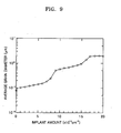
- FIG. 9 is a graph showing the relationship between the implanted amount of preamorphization material and the average diameter of grains in polysilicon.
- the graph of the FIG. 9 was disclosed in page 2422 in Journal of Applied Physics 59(2) 1986.
- the size of the grain in the polysilicon becomes larger in proportion to the implanted amount of preamorphization material.
- the largest amount of preamorphization material is implanted into the first amorphous silicon 13, and smallest amount of preamorphization material is implanted into the third amorphous silicon 33.
- the first polysilicon 15 formed on the first amorphous silicon 13 has the largest grain size, thereby, a microdefect flection pattern having a long period is formed for emitting and/or receiving red light, which has the longest wavelength. This will be described in more detail later.
- a second polysilicon 25 formed on the second amorphous silicon 23 may be formed with a grain size for forming a microdefect flection pattern having a period for emitting and/or receiving green light.
- a third polysilicon 35 formed on the third amorphous silicon 33 has a grain size for forming a microdefect flection pattern having a period for emitting and/or receiving blue light.
- groups of the first, the second and the third amorphous silicon 13, 23, 33 are formed as a two-dimensional array structure corresponding to the two-dimensional array of the silicon optoelectronic device.
- the arrangement of the region of the first, the second and the third amorphous silicon 13, 23, 33 may be modified in various ways.
- a panel for inputting and/or outputting light corresponding to a color image signal based on a pixel unit can be obtained by forming the region of the first, the second and the third amorphous silicon 13, 23, 33 as a two-dimensional array, transforming the amorphous silicon to the polysilicon by a high temperature process, and performing an oxidation process, an etching process, a doping process and an electrode patterning process, which will be explained later.
- the oxidation process i.e. a dry oxidation process, is performed as shown in FIG. 3, to form a silicon oxidation layer (SiO 2 ) 40 on the surface of the substrate where the first, the second and third polysilicon 15, 25 and 35 are formed.
- the oxidation process may be a dry oxidation process in a gas atmosphere containing O 2 and Cl 2 , at a high temperature of, for example, about 1150°C.
- the dry oxidation process is performed to several hours or several tens of hours.
- the oxidation process may also be a wet oxidation process.
- Nitrogen gas is basically injected into a vacuum chamber for the oxidation process to set the inner pressure of the vacuum chamber.
- the inner pressure of the vacuum chamber is set by using mainly oxygen gas O 2 and nitrogen gas N 2 .
- Chlorine gas Cl 2 of small amount compared with oxygen gas O 2 , for example, about 5 %, is included in the vacuum chamber.
- a microdefect flection pattern is formed at the interface between the silicon oxidation layer 40 and the substrate 1, due to acceleration of the oxidation by oxygen traveling through grain boundaries in the polysilicon.
- the technique related to oxidation of polysilicon is introduced in "Silicon Processing for the VLSI, Era vol. 1-Process Technology, page. 298" In the literature, it assumes that stress generated by the existence of the boundaries of grains accelerates the oxidation.
- the chlorine gas increases the oxidation rate during a dry oxidation process. That is, the chlorine gas accelerates the reaction or diffusion of oxidants at the interface between an oxidation layer i.e. the silicon oxidation layer 40, and a silicon layer i.e. the substrate 1.
- the chlorine gas traps and neutralizes nitrogen pollution in the oxidized layer.
- the chlorine gas also getters metallic impurities and stacking faults from the silicon layer. If more chlorine gas than the threshold concentration is included in the gas atmosphere, it causes the formation of additional phases at the interface between the oxidation layer and the silicon layer due to accumulation of gaseous oxidation products. Therefore, the interface between oxidation layer and silicon layer (SiO 2 /Si) becomes more rough.
- the first, the second and the third polysilicon 15, 25, 35 have different grain sizes.
- Magnified parts of FIG. 3 show exemplarily process that the interface between the silicon oxidation layer 40 and the substrate 1 is oxidized to be formed microdefect flection pattern having a period corresponding to the size of the grain by accelerating oxidation through the boundaries of the grains 15a, 25a, and 35a when the first polysilicon 15 has large grains 15a and the third polysilicon 35 has small grains.
- FIG. 3 shows exemplarily process that the interface between the silicon oxidation layer 40 and the substrate 1 is oxidized to be formed microdefect flection pattern having a period corresponding to the size of the grain by accelerating oxidation through the boundaries of the grains 15a, 25a, and 35a when the first polysilicon 15 has large grains 15a and the third polysilicon 35 has small grains.
- a first microdefect flection pattern 51 having a long period is formed at the interface where the first polysilicon 15 is formed
- a third microdefect flection pattern 53 having a short period is formed at the interface where the third polysilicon 35 is formed.
- the second polysilicon 25, for example may have a grain size smaller than that of the first polysilicon 15 and larger than that of the third polysilicon 35.
- illustration with respect to a grain in the second polysilicon 25 and oxidation process through boundaries of grains in the second polysilicon 25 is omitted.
- the first, the second and the third microdefect flection patterns 51, 52, 53 are formed at the interface between the silicon oxidation layer 40 and the substrate 1 (SiO 2 /Si interface) where the first, the second and the third polysilicon 15, 25, 35 are formed as shown in a magnified part of FIG. 4.
- the grain sizes of the first, the second and the third polysilicon 15, 25, 35 are different, the period of the microdefects, that is the microcavity lengths in the first, the second and the third microdefect flection patterns are different.
- the microdefects of the first microdefect flection pattern 51 region may be formed to have a period to emit and/or to receive light of a red R wavelength region.
- the microdefects of the second microdefect flection pattern 52 region may be formed to have a period to emit and/or to receive light of green G wavelength region.
- the microdefect of the third microdefect flection pattern 53 region may be formed to have a period to emit and/or to receive light of blue B wavelength region.
- an etching process is performed as shown in FIGS. 5A and 5B. That is, regions of the silicon oxidation layer 40 where the first, the second and the third polysilicon 15, 25, 35 are formed are etched to expose the first, the second and the third microdefect flection patterns 40a, 40b, 40c formed at the interface between the silicon oxidation layer 40 and the substrate 1. The exposed region is bigger than the regions where the first, the second and the third polysilicon 15, 25, 35 are formed. The first, the second and the third microdefect flection patterns are exaggerated in FIGS. 5A and 5B.
- a photoresist layer 60 is formed on the silicon oxidation layer 40 and patterned to expose regions corresponding to the first, the second and the third polysilicon 15, 25, 35 of the silicon oxidation layer 40. After patterning, the exposed silicon oxidation layer 40 region is etched, and then the photoresist layer 60 is eliminated. As a result, the pattern of the silicon oxidation layer 4 having openings 40a, 40b, 40c obtained by eliminating the regions of the silicon oxidation layer 40 where the first, the second and the third polysilicon 15, 25, 35 are formed is obtained as shown in FIG. 5B.
- the first, the second and the third microdefect flection patterns 51, 53, 55 are doped with a dopant of the opposite type to the substrate 1, to 10 to 20 nm depth by using the pattern of the silicon oxidation layer 4 as a mask, thereby being formed first, second and third doping regions 71, 73 and 75.
- a dopant such as boron or phosphorous
- a dopant such as boron or phosphorous
- a non-equilibrium diffusion process there are formed ultra-shallowly doped region with the opposite type to the substrate 1, for example, a p+ type, along the surfaces of the first, the second and the third microdefect flection patterns 51, 53, 55.
- the first, the second and the third doping regions 71, 73, 75 having a quantum structure are formed at the p-n junction between doping region and the substrate 1.
- the magnified part of FIG. 6 shows the p-n junction between the substrate and the first doping region 71.
- the first, the second and the third microdefect flection patterns 15, 25, 35, and the first, the second and the third doping regions 71, 73, 75 are exaggerated.
- FIG. 10 shows a microdefect flection pattern and the quantum structure of a p-n junction region of a doping region ultra shallowly doped.
- the ultra-shallow doping regions 71, 73, 75 having the quantum structure at the p-n junction can also be used, while the doping regions can be formed to the desired shallow depth.
- the substrate 1 may be doped with a p type, and the first, the second and the third doping regions 71, 73, 75 may be doped with a n+ type.
- a quantum structure including at least one of a quantum well, a quantum dot and a quantum wire is formed at the interface between the doping regions of the substrate 1, i.e. a p-n junction. Therefore, the quantum confinement effect occurs at the p-n junction, thereby expressing the photoelectric conversion effect.
- Quantum wells are mostly formed at the p-n junction regions. Quantum dots or quantum wires may be formed at the p-n junction regions. A composite structure including two or more of the quantum well, the quantum dot and the quantum wire may also be formed at the p-n junction.
- doping regions of opposite conductivity types alternate with each other.
- the sizes of wells and barriers are respectively, for example, about 2 and 1 nm thick.
- Such ultra-shallow doping for forming the quantum structure at the p-n junction can be accomplished by optimally controlling diffusion temperature and deformed potential of a surface by structure of the microdefect flection patterns.
- the thickness of a diffusion profile can be adjusted to 10-20 nm by an appropriate diffusion temperature and a deformed potential due to the microdefect flection patterns formed along the surface of the substrate during diffusion.
- the quantum structure is created by the ultra-shallow diffusion profile thus formed.
- the silicon oxidation layer 40 exceeds a proper thickness e.g. several thousand angstrom ( ⁇ ), or the diffusion temperature is low, vacancies mainly affect diffusion, causing a deep diffusion.
- a proper thickness e.g. several thousand angstrom ( ⁇ )
- the diffusion temperature is low
- vacancies mainly affect diffusion, causing a deep diffusion.
- the silicon oxidation layer 40 is thinner than a proper thickness, or the diffusion temperature is high, silicon self-interstitials mainly affect diffusion, thereby causing a deep diffusion.
- the diffusion mechanism includes a kick-out mechanism by the self-interstitial and a vacancy mechanism by the vacancy, mainly.
- the silicon oxidation layer 40 works as a source providing the self-interstitial influencing on diffusion.
- diffusion is mostly generated by the kick-out mechanism by the self-interstitial
- the silicon oxidation layer 40 is thick, diffusion is mostly generated by the vacancy mechanism since the supplying amount of the self-interstitial is small. In above two cases, when the effect of Si self-interstitial or vacancy appears greatly, deep diffusion generates.
- the first, the second and the third doping regions 71, 73 and 75 are formed at the regions of the first, the second and the third microdefect flection patterns 51, 53 and 55 through the openings 40a, 40b, 40c of the silicon oxidation layer 40 pattern.
- the first, the second and the third microdefect flection patterns 51, 53, and 55 have different periods
- the first, the second and the third doping region 71, 73 and 75 are formed to have the periods for receiving and/or emitting light of, for example, red R, green G and blue B wavelengths.
- the silicon optoelectronic device includes an array of three silicon optoelectronic elements for emitting and/or receiving three different wavelengths, such as a first silicon optoelectronic element I for red light, a second silicon optoelectronic element II for green light and third silicon optoelectronic element III for blue light.
- a second electrode (not shown), that is, common electrode, is formed.
- the oxidation process is performed after forming the first, the second and the third polysilicon 15, 25, 35 having different grain sizes. Therefore, the microcavity length can be easily controlled and a single oxidation process can form the microdefect flection patterns having the microcavity for the red wavelength, the green wavelength and the blue wavelength. Therefore, an RGB optoelectronic device can be formed in a single wafer.
- a conventional method for forming naturally a microdefect flection pattern by controlling conditions of the oxidation process which was introduced in the U.S. Patent Application No.
- microdefect flection patterns for different colors must be formed on different wafers.
- three oxidation processes must be performed for forming microdefect flection patterns for red, green and blue. Accordingly, the conventional method takes about three times as long as the present invention for performing the oxidation process. Therefore, an optoelectronic device can be rapidly manufactured according to the method of the present invention because the number of oxidation processes having need of long time is reduced.
- samples of R, G, B must be prepared separately and then assembled for providing a white light.
- the optoelectronic devices for R, G and B can be embodied on single wafer as a pattern form.
- the method of manufacturing three adjacent silicon optoelectronic devices or a two-dimensional array structure of the three silicon optoelectronic devices for receiving and/or emitting red, green, and blue light on the substrate 1 is explained and shown above.
- the arrangement of the silicon optoelectronic devices on the substrate 1 may be modified in various ways.
- At least one optoelectronic device for single color light or a two-dimensional array structure of the same may be formed on the substrate 1.
- a silicon optoelectronic device for red, green or blue light may be formed on the substrate 1 by controlling the amount of preamorphization material implanted into the substrate 1 for forming amorphous silicon having a size of grain corresponding to the desired color light.
- FIG. 11 is a schematic view of one silicon optoelectronic device portion of a silicon optoelectronic device for emitting and/or receiving light of a plurality of wavelengths, which is manufactured by the processes shown in FIGS. 1 through 7.
- a first electrode 81 is formed on the surface of the substrate 1 where the doping regions 17, 73 and 75 are formed and a second electrode 85 is formed on the bottom of the substrate 1.
- Reference numerals common to the above-described drawings indicate substantially the same constitutional elements.
- FIG. 11 shows that the first electrode 81 is made of an opaque metal and contacts the external sides of the doping regions 71, 73 and 75.
- the first electrode 81 may also be made of a transparent electrode material such as indium tin oxide (ITO). In this case, the first electrode 81 may be formed on the entire surface of the doping regions 71, 73 and 75.
- ITO indium tin oxide
- the doping regions 71, 73, 75 are formed by forming the microdefect flection patterns at the interface between the silicon oxidation layer 40 and the substrate 1 by accelerating the oxidation through the grain boundaries in the polysilicon during oxidation process, exposing the resulting microdefect flection patterns by etching process, and ultra-shallowly doping the exposed microdefect flection patterns.
- the silicon optoelectronic device of the present invention can be used as a light-emitting device and/or light receiving device since the p-n junction formed between the doping regions 71, 73, 75 and the substrate 1 has a quantum structure at which the creation and recombination of electron-hole pairs occur.
- the silicon optoelectronic device may function as a light-emitting device as follows. For example, if an electric power (a voltage or a current) is applied across the first electrode 81 and the second electrode 85, carriers, i.e. electrons and holes, are injected into the quantum wells of the p-n junction and recombined (annihilated) at a subband energy level of the quantum wells. In this case, electroluminescence (EL) occurs at various wavelengths according to the recombination state of carriers, and only light of specific wavelength is amplified and emitted due to the microdefect period (microcavity length) of the microdefect flections 51, 53 and 55. The quantity of light generated varies depending on the voltage or current applied across the first and the second electrodes 81 and 85.
- EL electroluminescence
- the silicon optoelectronic device also may function as a light-receiving device as follows.
- the silicon optoelectronic device according to the present invention as described above has a high quantum efficiency since the quantum confinement effect occurs due to local variations in potential of charge distribution at the p-n junction of the ultra-shallow doping regions 71, 73 and 75 and a subband energy level is formed in the quantum well.
- the silicon optoelectronic device for emitting and/or receiving red, green and blue light at different doping regions can be obtained by forming the first, the second and the third polysilicons 15, 25, 35, performing the oxidation process for forming the first, the second and the third microdefect flection patterns 51, 53, 55 having different microcavity lengths corresponding to red, green and blue wavelength bands at the interface between the silicon oxidation layer 40 and the substrate 1, and performing the etching process and the doping process.
- an optoelectronic device omitting and/ore receiving lights of red, green and blue is generally required.
- the method of manufacturing the silicon optoelectronic device for wavelengths of red, green and blue is described and illustrated.
- the present invention can be applied to manufacture a silicon optoelectronic device for more than three wavelengths by forming a plurality of polysilicons having various grain sizes, by controlling the amount of preamorphization material implanted and performing the above mentioned processes.
- a silicon optoelectronic device may be manufactured to have superior characteristics for selecting and amplifying a specific wavelength band, because a microdefect flection pattern having desired microcavity length can be formed on the substrate 1.
- the amorphous silicon is formed by controlling the amount of preamorphization material implanted, and the amorphous silicon is transformed to polysilicon by a high temperature process, the polysilicon having a grain size corresponding to a desired wavelength band is obtained.
- the microdefect flection patterns are formed to have the desired microcavity length because the oxidation is accelerated through the boundaries of the grains of the polysilicon during oxidation process. Therefore, a silicon optoelectronic device for a specific wavelength band can be easily manufactured and uniformity and reproducibility are improved.
- microdefect flection pattern having regularly formed microdefects can be formed on the surface of the silicon optoelectronic device according to the present embodiment. It is also possible to amplify the light of specific wavelength band or attenuate the light of an unwanted wavelength band by regularly forming microdefects on the surface of the silicon optoelectronic device as mentioned above in comparison with a structure having irregular microdefect patterns or plane.
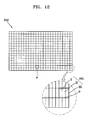
- FIG. 12 is a schematic plane diagram of an image input and/or output apparatus according to an embodiment of the present invention.
- the image input and/or output apparatus includes a silicon optoelectronic device panel 250 having a two-dimensional array of silicon optoelectronic devices 200, each of which leads to input and/or output of an image, formed on an n-type or a p-type silicon-based single substrate 1.
- image output means substantially an image display.
- image input means substantially the generation of an electric image signal by a camera photographing an object.
- the silicon optoelectronic device 200 includes first, second and third silicon optoelectronic elements I, II, III which are formed according to the manufacturing processes shown in FIGS. 1 through 7 for emitting and/or receiving red R, green G and blue B light.
- Each of the silicon optoelectronic elements I, II, III of the silicon optoelectronic device 200 functions as a light emitting and/or receiving device of a specific wavelength band due to the microcavity length of the microdefect flection pattern and the creation and recombination of electron-hole pairs by the quantum confinement effect at the p-n junction of the doping region which is ultra-shallowly doped along the surface of the microdefect flection pattern.
- a silicon optoelectronic device panel 250 for inputting and outputting an image by forming a two dimensional array of the silicon optoelectronic devices 200 on a single substrate 1 through a series of semiconductor manufacturing process.
- an electrode is patterned on the substrate 1 used as a base of the silicon optoelectronic device panel 250 so that the input and/or output of an image can be performed on a pixel-by-pixel basis in the silicon optoelectronic device panel 250 and thus an image of photographed object is converted into an electrical image signal and/or to display a two-dimensional image is displayed.
- a two-dimensional color image can be input and/or output by using the silicon optoelectronic device panel 250 where the silicon optoelectronic device 200 is arranged in a two-dimensional array.
- the silicon optoelectronic device 200 having the first, the second and the third silicon optoelectronic elements I, II, and III for red, green, and blue light is included in each pixel.
- the electrode is patterned on the substrate 1 for inputting and/or outputting an image for each pixel P in the silicon optoelectronic device panel 250.
- the color image can be provided without additional color filters.
- a color filter (not shown) on the front surface of the silicon optoelectronic device panel 250, to provide further clear color image.
- the image input and/or output device of the present invention may be modified in various ways as follows, in a view of inputting and outputting an image.
- the various modifications of the image input and/or output device in the view of inputting and outputting an image are originated from modification of circuit configurations of controlling to input and/or output image.
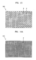
- an image input and/or output apparatus may be formed to input and output an image using image input pixels and image output pixels that are alternately arranged as shown in FIG. 13.
- pixels represented by oblique lines are image input pixels where a silicon optoelectronic device 200 of the present invention is used as a light-receiving device.
- Pixels represented by empty squares are image output pixels where a silicon optoelectronic device 200 of the present invention is used as a light-emitting device.
- the image input and/or output device of the present invention may be formed in such a way that some of the silicon optoelectronic devices 200 of the silicon optoelectronic device panel 250 input an image and the others output an image.
- the image input pixels and the image output pixels may have various arrangements. For example, pixels positioned at some areas of the silicon optoelectronic device panel 250 can be used as the image input pixels and the other pixels can be used as the image output pixels.
- the image input pixels and the image output pixels can be switched and the number of image input pixels and the image output pixels may also be altered when needed in an image input and/or output apparatus according to the present invention in which the input and output of an image are carried out by different silicon optoelectronic devices 200 as shown in FIG. 13. This is realized by appropriately designing the driving and/or control circuits and algorithms of an image input and/or output apparatus according to the present invention so that the image input pixels and the image output pixels are changed as necessary.
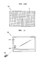
- Image input and/or output apparatus may also be formed in such a way that the input and output of an image can be carried out by the same silicon optoelectronic device 200 of the silicon optoelectronic device panel 250 at different times, as shown in FIGS. 14A and 14B.
- FIG. 14A shows an image input state of the silicon optoelectronic device panel 250 of an image input and/or output apparatus according to the present invention
- FIG. 14B shows an image output state of the silicon optoelectronic device panel 250 of an image input and/or output apparatus according to the present invention.
- an image input and/or output apparatus as described above can directly input optical information through a screen, it can be used in equipment for interactive visual communications and/or bidirectional information transmission, such as computer monitors, televisions, and in particular, digital televisions and handheld terminals.
- an image input and/or output apparatus allows the input and output of an image in a single panel, no separate camera is needed for visual communications.
- Handheld terminals may be various types of portable communication equipment such as mobile phones and personal digital assistants (PDAs).
- portable communication equipment such as mobile phones and personal digital assistants (PDAs).
- PDAs personal digital assistants
- an image input and/or output apparatus can input and output an image in a single panel, the full face of an operator can be photographed and transmitted. Therefore, vividness in visual communication is enhanced.
- an image input and/or output apparatus including a single silicon optoelectronic device panel having a two-dimensional array of silicon optoelectronic devices, but is not limited thereto. That is, an image input and/or output apparatus according to the present invention may include combinations of a plurality of silicon optoelectronic device panels to provide a larger screen.
- FIG. 15 shows a digital television using an image input and/or output apparatus according to the present invention.
- an image input and/or output apparatus can be used in a digital television 300 which allows for the input of information into a screen 310 and selection of a menu using an optical wireless remote controller 350.
- the optical wireless remote controller 350 irradiates a beam of light in specific area like a light pointer:
- a light signal is irradiated onto a specific region of the screen 310, for example, a menu 330, a silicon optoelectronic device in that region receives the light signal.
- changing channels of the digital television or working on the Internet is possible.
- an image input and/or output apparatus of the present invention can be applied to various equipment requiring bi-directional optical information transmission.
- the microcavity length can be easily controlled according to the present invention because the oxidation process is performed after forming a plurality of polysilicons having different grain sizes to form microdefect flection patterns having different microcavity lengths corresponding to the desired wavelengths. Therefore, according to the present invention, a silicon optoelectronic device having high wavelength selectivity is realized.
- a silicon optoelectronic device emitting and/or receiving light of different wavelengths in adjacent regions may be realized by performing an oxidation process, an etching process and a doping process after forming polysilicons having different grain sizes by controlling the amount of preamorphization material implanted at a plurality of regions.
- a microcavity length can be easily controlled and microdefect patterns suitable for red, green and blue light can be formed by a single oxidation process
- a silicon optoelectronic device for emitting and/or receiving red, green and blue light can be implemented on single wafer.
- a silicon optoelectronic device can be used as both a light-emitting device and a light-receiving device, an image input and/or output apparatus that can display an image and/or input an image or optical information in a single panel can be produced.
Abstract
Description
- The present invention relates to a method of manufacturing a silicon optoelectronic device, a silicon optoelectronic device manufactured by the method and an image input and/or output apparatus having the silicon optoelectronic device.
- An advantage of using a silicon semiconductor substrate is that it provides excellent reliability and allows a highly integrated density of logic device, an operation device, and a drive device on the substrate. Also, a silicon semiconductor material can be used to fabricate a highly integrated circuit at much lower cost than a compound semiconductor material, due to the use of inexpensive silicon. That is why many integrated circuits use silicon as their basic material.
- In this regard, current research into the fabrication of silicon-based light-emitting devices aims to make them compatible with integrated circuits and to obtain inexpensive photoelectronic devices.
- The present applicant has introduced a silicon optoelectronic device in U.S. Patent Application No. 10/122,421, filed on April 16, 2002. The silicon optoelectronic device includes an ultra-shallow doping region to form a quantum structure in a p-n junction of a silicon-based substrate. In this device, a period of surface flections i.e. microdefects enhancing wavelength selectivity, are formed by self-assembled under specific oxidation conditions and a specific diffusion process. For this reason, uniform production and reproduction of the microdefects are very difficult.
- As described in the U.S. Application No. 10/122,421, wavelength of the silicon optoelectronic device having the light emitting characteristics or/and light receiving characteristics due to the quantum structure formed by an ultra-shallow diffusion process is determined by the period of the microdefects, which is a microcavity length. Thus, the microdefects must be repeatedly arranged with a specific period to select the desired wavelength band.
- According to an aspect of the present invention, there is provided a method of manufacturing a silicon optoelectronic device, including: preparing an n-type or p-type silicon-based substrate; forming a polysilicon at one or more regions on the surface of the substrate; oxidizing the surface of the substrate where the polysilicon is formed to form a silicon oxidation layer on the substrate, and forming a microdefect flection pattern at the interface between the substrate and the silicon oxidation layer, wherein the microdefect flection pattern is formed by the oxidation during oxidation process accelerated by oxygen traveling through boundaries of the grains in the polysilicon; exposing the microdefect flection pattern by etching the silicon oxidation layer; and forming a doping region by doping the exposed microdefect flection pattern in an opposite type to the substrate.
- The forming of the polysilicon may include: forming an amorphous silicon by implanting a predetermined amount of a preamorphization material into the region of the substrate; and transforming the amorphous silicon to a polysilicon by a high temperature process.
- The preamorphization material may be a silicon ion or an inactive element.
- A microdefect of the microdefect flection pattern may be formed to have about single period for emitting and/or receiving light of a specific wavelength.
- The region where the polysilicon is formed may be a two-dimensional array, and an oxidation process, an etching process and a doping process are performed to form a two-dimensional array of silicon optoelectronic devices.
- The silicon optoelectronic device may be formed to include a plurality of silicon optoelectronic elements emitting and/or receiving light of a plurality of wavelengths by forming a plurality of polysilicons having different grain sizes through a plurality of repetition of polysilicon forming process on a plurality of regions of the substrate, forming a plurality of microdefect flection patterns having different periods by an oxidation process, and performing an etching process and a doping process
- A group of a plurality of polysilicons may be formed on the substrate as a two-dimensional array, and an oxidation process, an etching process and a doping process are performed to form a two-dimensional array of silicon optoelectronic device emitting and/or receiving light of a plurality of wavelengths.
- The plurality of polysilicons may be formed to have different grain sizes by implanting differently the amount of a preamorphization material.
- The preamorphization material may be a silicon ion or an inactive element.
- The preamorphization material may be a silicon ion or an inactive element.
- The method may further include forming an electrode pattern at the doping region, to be electrically connected to the doping region
- The doping region may be formed to have a quantum structure for generating an optoelectric conversion effect by a quantum confinement effect at a p-n junction between the doping region and the substrate.
- According to another aspect of the present invention, there is provided a silicon optoelectronic device manufactured by the above mentioned method.
- According to a further another aspect of the present invention, there is an image input and/or output apparatus, including: a silicon optoelectronic device panel formed by arranging silicon optoelectronic devices for inputting and/or outputting an image as a two-dimensional array on an n-type or p-type silicon-based substrate, wherein the silicon optoelectronic devices are manufactured by the above method.
- An electrode pattern may be formed on the substrate for inputting and/or outputting an image according to each pixel of a silicon optoelectronic panel.
- The silicon optoelectronic device may include a plurality of silicon optoelectronic elements for receiving and/or emitting light of different wavelengths, and one silicon optoelectronic device is included in each pixel of the silicon optoelectronic panel.
- The present invention provides a method of manufacturing a silicon optoelectronic device for increasing wavelength selectivity by controlling a microcavity length. The present invention also provides a silicon optoelectronic device manufactured by the method and an image input and/or output apparatus having the same.
- The above and other features and advantages of the present invention will become more apparent by describing in detail exemplary embodiments thereof with reference to the attached drawings in which:
- FIGS. 1 through 7 show a manufacturing process of a silicon optoelectronic device according to an embodiment of the present invention;
- FIG. 8 shows a polysilicon surface;
- FIG. 9 is a graph showing the relationship between the amount of an implanted preamorphization material and the average diameter of polysilicon grains;
- FIG. 10 shows a microdefect flection pattern and the quantum structure of a p-n junction region of an ultra-shallow doping region;
- FIG. 11 is a schematic view of a silicon optoelectronic device for emitting or/and receiving a plurality of wavelengths, which is manufactured by the processes shown in FIGS. 1 through 7;
- FIG. 12 is a schematic plane diagram of an image input and/or output device according to an embodiment of the present invention;
- FIG. 13 is a schematic plane diagram of an image input and/or output device in a view of inputting and outputting an image according to an embodiment of the present invention;
- FIGS. 14A and 14B shows an image input and/or output device in a view of inputting and outputting an image according to another embodiment of the present invention; and
- FIG. 15 shows a digital television using an image input and/or output apparatus according to the present invention.
- The present invention will now be described more fully with reference to the accompanying drawings, which show exemplary embodiments of a method of manufacturing a silicon optoelectronic device, a silicon optoelectronic device manufactured by the method, and an image input and/or output apparatus according to the present invention.
- FIGS. 1 through 7 show a manufacturing process of a silicon optoelectronic device according to an embodiment of the present invention.
- Referring to Fig. 1, an n-type or p-type silicon-based
substrate 1 is prepared. Thesubstrate 1 may be made of a semiconductor material containing silicon (Si), for example, Si or SiC. Thesubstrate 1 is doped with an n-type dopant. A silicon based wafer may be used as thesubstrate 1. Alternatively, thesubstrate 1 is made of a diamond. - Next, polysilicon is formed at regions of the surface of the
substrate 1 according to the manufacturing processes shown in FIGS. 2A through 2E. FIGS. 2A through 2E show an embodiment of a method of forming polysilicon having different grain sizes on three regions in thesubstrate 1, for obtaining microdefect flection patterns having different periods for emitting and/or receiving red, green and blue light. - Referring to FIG. 2A, a first
photoresist layer 11 is formed on thesubstrate 1 for forming afirst polysilicon 15 shown in FIG. 2E. - The first
photoresist layer 11 is formed to have openings in desiring region of the substrate to form thefirst polysilicon 15. The size of the opening is sub-micrometer. Thephotoresist layers - After forming the
photoresist layer 11 on thesubstrate 1, a firstamorphous silicon 13 is formed by implanting a Si preamorphization material through the opening of thephotoresist layer 11 into any region on thesubstrate 11. After forming the firstamorphous silicon 13, thephotoresist layer 11 is eliminated. The preamorphization material may be implanted based on an implant method. - After eliminating the
first photoresist layer 11, asecond photoresist layer 21 is formed on thesubstrate 1 where the firstamorphous silicon 13 is formed, as shown in FIG. 2B. Thesecond photoresist layer 21 also is formed to have an opening which matches to the region of thesubstrate 1 where asecond polysilicon 25 is shown in FIG. 2E. The opening of thesecond photoresist layer 21 is spaced apart from the firstamorphous silicon 13 formed in the region to form thefirst polysilicon 15. - After forming the
photoresist layer 21, the preamorphization material is implanted into a region of thesubstrate 1 through the opening of thephotoresist layer 21 so that a secondamorphous silicon 23 is formed. The amount of implanted preamorphization material for the secondamorphous silicon 23 is different from that for the firstamorphous silicon 13, as will be described later. After forming the secondamorphous silicon 23, thephotoresist layer 21 is eliminated. - After eliminating the
photoresist layer 21, aphotoresist layer 31 is formed on thesubstrate 1 where the first and the second amorphous silicons 13 and 23 are formed as shown in FIG. 2C. Thephotoresist layer 31 is formed to have an opening matching to the region of the substrate where a thirdamorphous silicon 35 of FIG. 2E is to be formed. The opening of thephotoresist layer 31 is spaced apart from the first and the secondamorphous silicon - After forming the
photoresist layer 31, the preamorphization material is implanted into a region of thesubstrate 1 through the opening of thephotoresist layer 31 so that a thirdamorphous silicon 33 is formed. The amount of the implanted preamorphization material for the thirdamorphous silicon 33 is different from that for the first and for the second amorphous silicons 13 and 23, as will be described later. After forming the thirdamorphous silicon 33, thephotoresist layer 31 is eliminated. - If the
photoresist layer 31 is eliminated, the first, the second and the thirdamorphous silicon substrate 1 is obtained, as shown in FIG. 2D. As described above, the first, the second and the thirdamorphous silicon amorphous silicon - After forming the
amorphous silicon substrate 1 is placed in a furnace and the temperature of the furnace increased to, for example, about 1150°C. Referring to FIG. 2E, the first, the second and the thirdamorphous silicon third polysilicon - As described above, the amorphous silicon is converted to polysilicon by the high temperature process. FIG. 8 shows the surface of the polysilicon. As shown in FIG. 8, there are a number of grains in the polysilicon. Oxygen can easily travel through boundaries of the grains in a following oxidation process. That is, the oxidation process is accelerated by the existence of the grains in the polysilicon.
- The preamorphization material may be silicon ions including Si2+ or Si3+, or an inactive element.
- The implanted amount of preamorphization material for forming the first, the second and the third
amorphous silicons third polysilicons - When a large amount of the preamorphization material is implanted, the grains in the polysilicon become larger. When the polysilicon includes large grains, a microdefect flection pattern of long period can be formed.
- FIG. 9 is a graph showing the relationship between the implanted amount of preamorphization material and the average diameter of grains in polysilicon. The graph of the FIG. 9 was disclosed in page 2422 in Journal of Applied Physics 59(2) 1986. As shown in FIG. 9, the size of the grain in the polysilicon becomes larger in proportion to the implanted amount of preamorphization material.
- Therefore, for example, when the formation of microdefect flection patterns having periods for emitting and/or receiving red light R, green light G and blue light B , respectively is desired in corresponding regions of the first, the second and the third
amorphous silicon amorphous silicon 13, and smallest amount of preamorphization material is implanted into the thirdamorphous silicon 33. In this case, thefirst polysilicon 15 formed on the firstamorphous silicon 13 has the largest grain size, thereby, a microdefect flection pattern having a long period is formed for emitting and/or receiving red light, which has the longest wavelength. This will be described in more detail later. Asecond polysilicon 25 formed on the secondamorphous silicon 23 may be formed with a grain size for forming a microdefect flection pattern having a period for emitting and/or receiving green light. Athird polysilicon 35 formed on the thirdamorphous silicon 33 has a grain size for forming a microdefect flection pattern having a period for emitting and/or receiving blue light. - When the silicon optoelectronic device is formed as two-dimensional array, groups of the first, the second and the third
amorphous silicon amorphous silicon amorphous silicon - After forming the polysilicons, the oxidation process, i.e. a dry oxidation process, is performed as shown in FIG. 3, to form a silicon oxidation layer (SiO2) 40 on the surface of the substrate where the first, the second and
third polysilicon - The oxidation process may be a dry oxidation process in a gas atmosphere containing O2 and Cl2, at a high temperature of, for example, about 1150°C. The dry oxidation process is performed to several hours or several tens of hours. The oxidation process may also be a wet oxidation process.
- Nitrogen gas is basically injected into a vacuum chamber for the oxidation process to set the inner pressure of the vacuum chamber. The inner pressure of the vacuum chamber is set by using mainly oxygen gas O2 and nitrogen gas N2. Chlorine gas Cl2 of small amount compared with oxygen gas O2, for example, about 5 %, is included in the vacuum chamber.
- While forming the
silicon oxidation layer 40, a microdefect flection pattern is formed at the interface between thesilicon oxidation layer 40 and thesubstrate 1, due to acceleration of the oxidation by oxygen traveling through grain boundaries in the polysilicon. The technique related to oxidation of polysilicon is introduced in "Silicon Processing for the VLSI, Era vol. 1-Process Technology, page. 298" In the literature, it assumes that stress generated by the existence of the boundaries of grains accelerates the oxidation. - The chlorine gas increases the oxidation rate during a dry oxidation process. That is, the chlorine gas accelerates the reaction or diffusion of oxidants at the interface between an oxidation layer i.e. the
silicon oxidation layer 40, and a silicon layer i.e. thesubstrate 1. The chlorine gas traps and neutralizes nitrogen pollution in the oxidized layer. The chlorine gas also getters metallic impurities and stacking faults from the silicon layer. If more chlorine gas than the threshold concentration is included in the gas atmosphere, it causes the formation of additional phases at the interface between the oxidation layer and the silicon layer due to accumulation of gaseous oxidation products. Therefore, the interface between oxidation layer and silicon layer (SiO2/Si) becomes more rough. - Since such existence of chlorine gas makes the interface between the oxidation layer and silicon layer further rough, sure microdefect flection patterns can be obtained and a high quality
silicon oxidation layer 40 can be formed. - Referring to FIG. 3 again, the first, the second and the
third polysilicon silicon oxidation layer 40 and thesubstrate 1 is oxidized to be formed microdefect flection pattern having a period corresponding to the size of the grain by accelerating oxidation through the boundaries of thegrains first polysilicon 15 haslarge grains 15a and thethird polysilicon 35 has small grains. As shown exemplarily in FIG. 3, when thefirst polysilicon 15 haslarge grains 15a and thethird polysilicon 35 hassmall grains 35a, a firstmicrodefect flection pattern 51 having a long period is formed at the interface where thefirst polysilicon 15 is formed, and a thirdmicrodefect flection pattern 53 having a short period is formed at the interface where thethird polysilicon 35 is formed. Thesecond polysilicon 25, for example, may have a grain size smaller than that of thefirst polysilicon 15 and larger than that of thethird polysilicon 35. Here, illustration with respect to a grain in thesecond polysilicon 25 and oxidation process through boundaries of grains in thesecond polysilicon 25 is omitted. - When the structure of the
substrate 1 and thesilicon oxidation layer 40 is formed by oxidizing thesubstrate 1 to constant thickness through oxidation process as mentioned above, the first, the second and the thirdmicrodefect flection patterns silicon oxidation layer 40 and the substrate 1 (SiO2/Si interface) where the first, the second and thethird polysilicon - Since the grain sizes of the first, the second and the
third polysilicon - The microdefects of the first
microdefect flection pattern 51 region, for example, may be formed to have a period to emit and/or to receive light of a red R wavelength region. The microdefects of the second microdefect flection pattern 52 region may be formed to have a period to emit and/or to receive light of green G wavelength region. The microdefect of the thirdmicrodefect flection pattern 53 region may be formed to have a period to emit and/or to receive light of blue B wavelength region. - After performing the oxidation process as described above, an etching process is performed as shown in FIGS. 5A and 5B. That is, regions of the
silicon oxidation layer 40 where the first, the second and thethird polysilicon microdefect flection patterns silicon oxidation layer 40 and thesubstrate 1. The exposed region is bigger than the regions where the first, the second and thethird polysilicon - Referring to FIG. 5A, a
photoresist layer 60 is formed on thesilicon oxidation layer 40 and patterned to expose regions corresponding to the first, the second and thethird polysilicon silicon oxidation layer 40. After patterning, the exposedsilicon oxidation layer 40 region is etched, and then thephotoresist layer 60 is eliminated. As a result, the pattern of the silicon oxidation layer 4 havingopenings silicon oxidation layer 40 where the first, the second and thethird polysilicon - Referring to FIG. 6, after patterning of the
silicon oxidation layer 40, the first, the second and the thirdmicrodefect flection patterns substrate 1, to 10 to 20 nm depth by using the pattern of the silicon oxidation layer 4 as a mask, thereby being formed first, second andthird doping regions - When a dopant such as boron or phosphorous is injected into the
substrate 1 through theopenings silicon oxidation layer 40 pattern, for example, by a non-equilibrium diffusion process, there are formed ultra-shallowly doped region with the opposite type to thesubstrate 1, for example, a p+ type, along the surfaces of the first, the second and the thirdmicrodefect flection patterns - As a result, the first, the second and the
third doping regions substrate 1. The magnified part of FIG. 6 shows the p-n junction between the substrate and thefirst doping region 71. In FIG. 6, the first, the second and the thirdmicrodefect flection patterns third doping regions - Although a non-equilibrium diffusion process is used here for the formation of the
ultra-shallow doping regions - The
substrate 1 may be doped with a p type, and the first, the second and thethird doping regions - As mentioned above, when the doping process is controlled so that the doping regions are formed to an ultra-shallow depth, a quantum structure including at least one of a quantum well, a quantum dot and a quantum wire is formed at the interface between the doping regions of the
substrate 1, i.e. a p-n junction. Therefore, the quantum confinement effect occurs at the p-n junction, thereby expressing the photoelectric conversion effect. - Quantum wells are mostly formed at the p-n junction regions. Quantum dots or quantum wires may be formed at the p-n junction regions. A composite structure including two or more of the quantum well, the quantum dot and the quantum wire may also be formed at the p-n junction.
- At the quantum structure of the p-n junction, doping regions of opposite conductivity types alternate with each other. The sizes of wells and barriers are respectively, for example, about 2 and 1 nm thick.
- Such ultra-shallow doping for forming the quantum structure at the p-n junction can be accomplished by optimally controlling diffusion temperature and deformed potential of a surface by structure of the microdefect flection patterns.
- The thickness of a diffusion profile can be adjusted to 10-20 nm by an appropriate diffusion temperature and a deformed potential due to the microdefect flection patterns formed along the surface of the substrate during diffusion. The quantum structure is created by the ultra-shallow diffusion profile thus formed.
- As is well known in the field of diffusion technology, when the
silicon oxidation layer 40 exceeds a proper thickness e.g. several thousand angstrom (Å), or the diffusion temperature is low, vacancies mainly affect diffusion, causing a deep diffusion. On the other hand, when thesilicon oxidation layer 40 is thinner than a proper thickness, or the diffusion temperature is high, silicon self-interstitials mainly affect diffusion, thereby causing a deep diffusion. - The diffusion mechanism includes a kick-out mechanism by the self-interstitial and a vacancy mechanism by the vacancy, mainly. The
silicon oxidation layer 40 works as a source providing the self-interstitial influencing on diffusion. When thesilicon oxidation layer 40 is thin, diffusion is mostly generated by the kick-out mechanism by the self-interstitial, and when thesilicon oxidation layer 40 is thick, diffusion is mostly generated by the vacancy mechanism since the supplying amount of the self-interstitial is small. In above two cases, when the effect of Si self-interstitial or vacancy appears greatly, deep diffusion generates. - However, when a
silicon oxidation layer 40 is formed to an appropriate thickness to be generated Si self-interstitial and vacancy in a similar ratio, a combination of the silicon self-interstitials and the vacancies do not accelerate dopant diffusion. As a result, an ultra-shallow doping is accomplished. The physical properties of the vacancies and the self-interstitials as used herein are well disclosed in the field of the diffusion technology, and thus, the detailed description thereof will be omitted. - When the conditions which vacancy and silicon self-interstitial do not influence on dopant diffusion are satisfied, ultra-shallow doping depth of several tens nm can be accomplished.
- By the above mentioned doping process, the first, the second and the
third doping regions microdefect flection patterns openings silicon oxidation layer 40 pattern. In this case, since the first, the second and the thirdmicrodefect flection patterns third doping region - Lastly, when a
first electrode pattern 81 is formed on thesubstrate 1 to be electrically connected to the first, the second and thethird doping regions substrate 1; a second electrode (not shown), that is, common electrode, is formed. - In the method of manufacturing the silicon optoelectronic device according to the present invention, the oxidation process is performed after forming the first, the second and the
third polysilicon - Furthermore, in the case of a microdefect flection pattern self-assembled along the surface of a substrate by controlling the conditions of an oxidation process, which was introduced in the U.S. Patent Application No. 10/122,421, samples of R, G, B must be prepared separately and then assembled for providing a white light. In the present invention, the optoelectronic devices for R, G and B can be embodied on single wafer as a pattern form.
- The method of manufacturing three adjacent silicon optoelectronic devices or a two-dimensional array structure of the three silicon optoelectronic devices for receiving and/or emitting red, green, and blue light on the
substrate 1 is explained and shown above. However, the arrangement of the silicon optoelectronic devices on thesubstrate 1 may be modified in various ways. - Also, at least one optoelectronic device for single color light or a two-dimensional array structure of the same may be formed on the
substrate 1. For example, a silicon optoelectronic device for red, green or blue light may be formed on thesubstrate 1 by controlling the amount of preamorphization material implanted into thesubstrate 1 for forming amorphous silicon having a size of grain corresponding to the desired color light. - When forming at least one optoelectronic device for single color light or a two-dimensional array structure of the same on the
substrate 1, the processes shown in FIGS. 2B and 2C can be omitted because only one type of amorphous silicon is formed. - FIG. 11 is a schematic view of one silicon optoelectronic device portion of a silicon optoelectronic device for emitting and/or receiving light of a plurality of wavelengths, which is manufactured by the processes shown in FIGS. 1 through 7.
- Referring to FIG. 11, a
first electrode 81 is formed on the surface of thesubstrate 1 where thedoping regions second electrode 85 is formed on the bottom of thesubstrate 1. Reference numerals common to the above-described drawings indicate substantially the same constitutional elements. FIG. 11 shows that thefirst electrode 81 is made of an opaque metal and contacts the external sides of thedoping regions first electrode 81 may also be made of a transparent electrode material such as indium tin oxide (ITO). In this case, thefirst electrode 81 may be formed on the entire surface of thedoping regions - In the silicon optoelectronic device shown in FIG. 11, the
doping regions silicon oxidation layer 40 and thesubstrate 1 by accelerating the oxidation through the grain boundaries in the polysilicon during oxidation process, exposing the resulting microdefect flection patterns by etching process, and ultra-shallowly doping the exposed microdefect flection patterns. - The silicon optoelectronic device of the present invention can be used as a light-emitting device and/or light receiving device since the p-n junction formed between the
doping regions substrate 1 has a quantum structure at which the creation and recombination of electron-hole pairs occur. - The silicon optoelectronic device may function as a light-emitting device as follows. For example, if an electric power (a voltage or a current) is applied across the
first electrode 81 and thesecond electrode 85, carriers, i.e. electrons and holes, are injected into the quantum wells of the p-n junction and recombined (annihilated) at a subband energy level of the quantum wells. In this case, electroluminescence (EL) occurs at various wavelengths according to the recombination state of carriers, and only light of specific wavelength is amplified and emitted due to the microdefect period (microcavity length) of the microdefect flections 51, 53 and 55. The quantity of light generated varies depending on the voltage or current applied across the first and thesecond electrodes - The silicon optoelectronic device also may function as a light-receiving device as follows. When only light of a specific wavelength band according to the microdefect period of the microdefect flection pattern artificially formed is incident on the p-n junction and photons are absorbed in the p-n junction of the quantum well structure, electrons and holes are excited at a subband energy level of the quantum well. Therefore, when an external circuit (not shown), for example, load resistance is connected to an output terminal, a current proportional to the quantity of received light is output.
- The silicon optoelectronic device according to the present invention as described above has a high quantum efficiency since the quantum confinement effect occurs due to local variations in potential of charge distribution at the p-n junction of the
ultra-shallow doping regions - As described above, the silicon optoelectronic device for emitting and/or receiving red, green and blue light at different doping regions can be obtained by forming the first, the second and the
third polysilicons microdefect flection patterns silicon oxidation layer 40 and thesubstrate 1, and performing the etching process and the doping process. - For realizing color image, an optoelectronic device omitting and/ore receiving lights of red, green and blue is generally required. In consideration of this requirement, in the present embodiment above described, the method of manufacturing the silicon optoelectronic device for wavelengths of red, green and blue is described and illustrated. However, this is only example. That is, the present invention can be applied to manufacture a silicon optoelectronic device for more than three wavelengths by forming a plurality of polysilicons having various grain sizes, by controlling the amount of preamorphization material implanted and performing the above mentioned processes.
- According to the present invention, a silicon optoelectronic device may be manufactured to have superior characteristics for selecting and amplifying a specific wavelength band, because a microdefect flection pattern having desired microcavity length can be formed on the
substrate 1. - As described above, in the conventional method introduced in U.S. Patent Application No. 10/122,421, it was not easy to control the microcavity length because the microcavity was self-assembled during process. It is easily generated that microcavities for various wavelengths were mixed, and the process conditions for selecting a specific wavelength could not be easily defined.
- However, in the present invention, since the amorphous silicon is formed by controlling the amount of preamorphization material implanted, and the amorphous silicon is transformed to polysilicon by a high temperature process, the polysilicon having a grain size corresponding to a desired wavelength band is obtained. After forming the polysilicon, the microdefect flection patterns are formed to have the desired microcavity length because the oxidation is accelerated through the boundaries of the grains of the polysilicon during oxidation process. Therefore, a silicon optoelectronic device for a specific wavelength band can be easily manufactured and uniformity and reproducibility are improved.
- Especially, it is possible to filter only the light of specific wavelength band because a microdefect flection pattern having regularly formed microdefects can be formed on the surface of the silicon optoelectronic device according to the present embodiment. It is also possible to amplify the light of specific wavelength band or attenuate the light of an unwanted wavelength band by regularly forming microdefects on the surface of the silicon optoelectronic device as mentioned above in comparison with a structure having irregular microdefect patterns or plane.
- Hereinafter, an image input and/or output apparatus will be explained as an embodiment of a device having the silicon optoelectronic device array according to the present invention.
- FIG. 12 is a schematic plane diagram of an image input and/or output apparatus according to an embodiment of the present invention.
- Referring to FIG. 12, the image input and/or output apparatus according to the present invention includes a silicon
optoelectronic device panel 250 having a two-dimensional array of siliconoptoelectronic devices 200, each of which leads to input and/or output of an image, formed on an n-type or a p-type silicon-basedsingle substrate 1. The term, "image output" as used herein means substantially an image display. The term, "image input" as used herein means substantially the generation of an electric image signal by a camera photographing an object. - The
silicon optoelectronic device 200 includes first, second and third silicon optoelectronic elements I, II, III which are formed according to the manufacturing processes shown in FIGS. 1 through 7 for emitting and/or receiving red R, green G and blue B light. - Each of the silicon optoelectronic elements I, II, III of the
silicon optoelectronic device 200 functions as a light emitting and/or receiving device of a specific wavelength band due to the microcavity length of the microdefect flection pattern and the creation and recombination of electron-hole pairs by the quantum confinement effect at the p-n junction of the doping region which is ultra-shallowly doped along the surface of the microdefect flection pattern. - Accordingly, it is possible to manufacture a silicon
optoelectronic device panel 250 for inputting and outputting an image by forming a two dimensional array of the siliconoptoelectronic devices 200 on asingle substrate 1 through a series of semiconductor manufacturing process. - In this case, an electrode is patterned on the
substrate 1 used as a base of the siliconoptoelectronic device panel 250 so that the input and/or output of an image can be performed on a pixel-by-pixel basis in the siliconoptoelectronic device panel 250 and thus an image of photographed object is converted into an electrical image signal and/or to display a two-dimensional image is displayed. - Accordingly, a two-dimensional color image can be input and/or output by using the silicon
optoelectronic device panel 250 where thesilicon optoelectronic device 200 is arranged in a two-dimensional array. In this case, thesilicon optoelectronic device 200 having the first, the second and the third silicon optoelectronic elements I, II, and III for red, green, and blue light is included in each pixel. - As mentioned above, the electrode is patterned on the
substrate 1 for inputting and/or outputting an image for each pixel P in the siliconoptoelectronic device panel 250. - By using the silicon
optoelectronic device panel 250, the color image can be provided without additional color filters. - It is possible to further include a color filter (not shown) on the front surface of the silicon
optoelectronic device panel 250, to provide further clear color image. - The image input and/or output device of the present invention may be modified in various ways as follows, in a view of inputting and outputting an image. The various modifications of the image input and/or output device in the view of inputting and outputting an image are originated from modification of circuit configurations of controlling to input and/or output image.
- That is, an image input and/or output apparatus according to the present invention may be formed to input and output an image using image input pixels and image output pixels that are alternately arranged as shown in FIG. 13. In FIG. 13, pixels represented by oblique lines are image input pixels where a
silicon optoelectronic device 200 of the present invention is used as a light-receiving device. Pixels represented by empty squares are image output pixels where asilicon optoelectronic device 200 of the present invention is used as a light-emitting device. - As shown in FIG. 13, the image input and/or output device of the present invention may be formed in such a way that some of the silicon
optoelectronic devices 200 of the siliconoptoelectronic device panel 250 input an image and the others output an image. - The image input pixels and the image output pixels may have various arrangements. For example, pixels positioned at some areas of the silicon
optoelectronic device panel 250 can be used as the image input pixels and the other pixels can be used as the image output pixels. - Since the silicon
optoelectronic devices 200 can be used as light-emitting and receiving devices, the image input pixels and the image output pixels can be switched and the number of image input pixels and the image output pixels may also be altered when needed in an image input and/or output apparatus according to the present invention in which the input and output of an image are carried out by different siliconoptoelectronic devices 200 as shown in FIG. 13. This is realized by appropriately designing the driving and/or control circuits and algorithms of an image input and/or output apparatus according to the present invention so that the image input pixels and the image output pixels are changed as necessary. - Image input and/or output apparatus according to the present invention may also be formed in such a way that the input and output of an image can be carried out by the same
silicon optoelectronic device 200 of the siliconoptoelectronic device panel 250 at different times, as shown in FIGS. 14A and 14B. FIG. 14A shows an image input state of the siliconoptoelectronic device panel 250 of an image input and/or output apparatus according to the present invention and FIG. 14B shows an image output state of the siliconoptoelectronic device panel 250 of an image input and/or output apparatus according to the present invention. - While an image input and/or output apparatus according to the present invention has been particularly shown and described with reference to exemplary embodiments thereof, various changes may be made therein without departing from the scope of the present invention.
- Since an image input and/or output apparatus according to the present invention as described above can directly input optical information through a screen, it can be used in equipment for interactive visual communications and/or bidirectional information transmission, such as computer monitors, televisions, and in particular, digital televisions and handheld terminals.
- In this case, since an image input and/or output apparatus according to the present invention allows the input and output of an image in a single panel, no separate camera is needed for visual communications.
- Handheld terminals may be various types of portable communication equipment such as mobile phones and personal digital assistants (PDAs).
- Furthermore, since an image input and/or output apparatus according to the present invention can input and output an image in a single panel, the full face of an operator can be photographed and transmitted. Therefore, vividness in visual communication is enhanced.
- Up until now, the present invention has been described with a view to an image input and/or output apparatus including a single silicon optoelectronic device panel having a two-dimensional array of silicon optoelectronic devices, but is not limited thereto. That is, an image input and/or output apparatus according to the present invention may include combinations of a plurality of silicon optoelectronic device panels to provide a larger screen.
- FIG. 15 shows a digital television using an image input and/or output apparatus according to the present invention.
- Referring to FIG. 15, an image input and/or output apparatus according to the present invention can be used in a
digital television 300 which allows for the input of information into ascreen 310 and selection of a menu using an optical wirelessremote controller 350. The optical wirelessremote controller 350 irradiates a beam of light in specific area like a light pointer: When a light signal is irradiated onto a specific region of thescreen 310, for example, amenu 330, a silicon optoelectronic device in that region receives the light signal. According to the received light signal, changing channels of the digital television or working on the Internet is possible. - In addition, an image input and/or output apparatus of the present invention can be applied to various equipment requiring bi-directional optical information transmission.
- As is apparent from the above description, the microcavity length can be easily controlled according to the present invention because the oxidation process is performed after forming a plurality of polysilicons having different grain sizes to form microdefect flection patterns having different microcavity lengths corresponding to the desired wavelengths. Therefore, according to the present invention, a silicon optoelectronic device having high wavelength selectivity is realized.
- In addition, according to the present invention, a silicon optoelectronic device emitting and/or receiving light of different wavelengths in adjacent regions may be realized by performing an oxidation process, an etching process and a doping process after forming polysilicons having different grain sizes by controlling the amount of preamorphization material implanted at a plurality of regions.
- Accordingly, since a microcavity length can be easily controlled and microdefect patterns suitable for red, green and blue light can be formed by a single oxidation process, a silicon optoelectronic device for emitting and/or receiving red, green and blue light can be implemented on single wafer.
- Furthermore, since a silicon optoelectronic device according to the present invention can be used as both a light-emitting device and a light-receiving device, an image input and/or output apparatus that can display an image and/or input an image or optical information in a single panel can be produced.
- While the present invention has been particularly shown and described with reference to exemplary embodiments thereof, it will be understood by those of ordinary skill in the art that various changes in form and details may be made therein without departing from the scope of the present invention as defined by the following claims.
Claims (22)
- A method of manufacturing a silicon optoelectronic device, comprising:preparing an n-type or p-type silicon-based substrate;forming a polysilicon at one or more regions on the surface of the substrate;oxidizing the surface of the substrate where the polysilicon is formed to form a silicon oxidation layer on the substrate, and forming a microdefect flection pattern at the interface between the substrate and the silicon oxidation layer, wherein the microdefect flection pattern is formed by the oxidation during the oxidation process accelerated by oxygen traveling through boundaries of the grains in the polysilicon;exposing the microdefect flection pattern by etching the silicon oxidation layer; andforming a doping region by doping the exposed microdefect flection pattern in an opposite type to the substrate.
- The method of claim 1, wherein forming the polysilicon includes:forming an amorphous silicon by implanting a predetermined amount of a preamorphization material into the region of the substrate; andtransforming the amorphous silicon to a polysilicon by a high temperature process.
- The method of claim 2, wherein the preamorphization material is a silicon ion or an inactive element.
- The method of claim 2 or 3, wherein a microdefect of the microdefect flection pattern is formed to have about single period for emitting and/or receiving light of a specific wavelength.
- The method of claim 4, wherein the region where the polysilicon is formed is a two-dimensional array, and an oxidation process, an etching process and a doping process are performed to form a two-dimensional array of silicon optoelectronic devices.
- The method of any of claims 2 to 4, wherein the silicon optoelectronic device is formed to include a plurality of silicon optoelectronic elements emitting and/or receiving light of a plurality of wavelengths by forming a plurality of polysilicons having different grain sizes through a plurality of repetition of polysilicon forming process on a plurality of regions of the substrate, forming a plurality of microdefect flection patterns having different periods by an oxidation process, and performing an etching process and a doping process
- The method of claim 6, wherein a group of a plurality of polysilicons is formed on the substrate as a two-dimensional array, and an oxidation process, an etching process and a doping process are performed to form a two-dimensional array of silicon optoelectronic device emitting and/or receiving light of a plurality of wavelengths.
- The method of claim 6, wherein the plurality of polysilicons is formed to have different grain sizes by implanting differently the amount of a preamorphization material.
- The method of any of claims 2 to 8, wherein the preamorphization material is a silicon ion or an inactive element.
- The method of any preceding claim, wherein the oxidation process is performed in a gas atmosphere containing oxygen and chlorine gas.
- The method of any one of claims 1 through 10, further comprising forming an electrode pattern at the doping region, to be electrically connected to the doping region.
- The method of any one of claims 1 through 11, wherein the doping region is formed to have a quantum structure for generating an optoelectric conversion effect by a quantum confinement effect at a p-n junction between the doping region and the substrate.
- The method of claim 12, wherein the doping region is formed by a non-equilibrium of dopant.
- A silicon optoelectronic device manufactured by the method of any one of claims 1 through 13.
- The silicon optoelectronic device of claim 14, wherein the doping region is formed to have a quantum structure generating an optoelectric conversion effect by a quantum confinement effect at a p-n junction between the doping region and the substrate.
- The silicon optoelectronic device of claim 15, wherein the doping region is formed by a non-equilibrium of dopant.
- The silicon optoelectronic device of claim 14, further comprising an electrode pattern in the doping region to be electrically connected to the doping region.
- An image input and/or output apparatus, comprising:a silicon optoelectronic device panel formed by arranging silicon optoelectronic devices for inputting and/or outputting an image as a two-dimensional array on an n-type or p-type silicon-based substrate,wherein the silicon optoelectronic devices are the silicon optoelectronic devices of claim 16.
- The mage input and/or output apparatus of claim 18, wherein the doping region is to have a quantum structure generating an optoelectric conversion effect by a quantum confinement effect at a p-n junction between the doping region and the substrate.
- The image input and/or output apparatus of claim 19, wherein the doping region is formed by a non-equilibrium of dopant.
- The image input and/or output apparatus of claim 18, wherein an electrode pattern is formed on the substrate for inputting and/or outputting an image according to each pixel from a silicon optoelectronic device panel.
- The image input and/or output apparatus of claim 18, wherein the silicon optoelectronic device includes a plurality of silicon optoelectronic elements for receiving and/or emitting light of different wavelengths, and one silicon optoelectronic device is included in each pixel of the silicon optoelectronic panel.
Applications Claiming Priority (1)
| Application Number | Priority Date | Filing Date | Title |
|---|---|---|---|
| KR1020040097007A KR100612875B1 (en) | 2004-11-24 | 2004-11-24 | Silicon optoelectronic device manufacturing method and Silicon optoelectronic device manufactured by thereof and Image input and/or output apparatus applied it |
Publications (2)
| Publication Number | Publication Date |
|---|---|
| EP1662586A2 true EP1662586A2 (en) | 2006-05-31 |
| EP1662586A3 EP1662586A3 (en) | 2009-03-11 |
Family
ID=35892266
Family Applications (1)
| Application Number | Title | Priority Date | Filing Date |
|---|---|---|---|
| EP05257069A Withdrawn EP1662586A3 (en) | 2004-11-24 | 2005-11-16 | Silicon optoelectronic device, manufacturing method thereof, and image input and/or output apparatus using the same |
Country Status (5)
| Country | Link |
|---|---|
| US (1) | US7670862B2 (en) |
| EP (1) | EP1662586A3 (en) |
| JP (1) | JP2006148142A (en) |
| KR (1) | KR100612875B1 (en) |
| CN (1) | CN1780007A (en) |
Cited By (1)
| Publication number | Priority date | Publication date | Assignee | Title |
|---|---|---|---|---|
| WO2008122877A2 (en) * | 2007-04-05 | 2008-10-16 | Technomedica Ag | Solid-state radiation source, production and use thereof |
Families Citing this family (5)
| Publication number | Priority date | Publication date | Assignee | Title |
|---|---|---|---|---|
| KR100940530B1 (en) * | 2003-01-17 | 2010-02-10 | 삼성전자주식회사 | Silicon optoelectronic device manufacturing method and Silicon optoelectronic device manufactured by thereof and Image input and/or output apparatus applied it |
| KR100612875B1 (en) | 2004-11-24 | 2006-08-14 | 삼성전자주식회사 | Silicon optoelectronic device manufacturing method and Silicon optoelectronic device manufactured by thereof and Image input and/or output apparatus applied it |
| KR20060059327A (en) * | 2004-11-27 | 2006-06-01 | 삼성전자주식회사 | Silicon optoelectronic device manufacturing method and silicon optoelectronic device manufactured by thereof and image input and/or output apparatus applied it |
| US8748908B2 (en) | 2012-05-07 | 2014-06-10 | Sufian Abedrabbo | Semiconductor optical emission device |
| DE102020111371A1 (en) * | 2020-02-27 | 2021-09-02 | Taiwan Semiconductor Manufacturing Co. Ltd. | ABSORPTION ENRICHMENT STRUCTURE TO INCREASE THE QUANTUM EFFICIENCY OF AN IMAGE SENSOR |
Citations (8)
| Publication number | Priority date | Publication date | Assignee | Title |
|---|---|---|---|---|
| US4013465A (en) * | 1973-05-10 | 1977-03-22 | Secretary Of State For Defence In Her Britannic Majesty's Government Of The United Kingdom Of Great Britain And Northern Ireland | Reducing the reflectance of surfaces to radiation |
| KR20010061354A (en) * | 1999-12-28 | 2001-07-07 | 박종섭 | Method for fabricating photodiode of image sensor |
| US6278145B1 (en) * | 1999-06-25 | 2001-08-21 | Mitsubishi Denki Kabushiki Kaisha | PN junction diode having enhanced light-gathering efficiency |
| US6359323B1 (en) * | 1998-12-30 | 2002-03-19 | Hyundai Electronics Industries Co., Ltd. | Color image sensor and method for fabricating the same |
| US20020135869A1 (en) * | 2000-11-03 | 2002-09-26 | Michele Banish | Anti-reflective structures |
| EP1328024A2 (en) * | 2002-01-10 | 2003-07-16 | Samsung Electronics Co. Ltd. | Silicon optoelectronic device and light emitting device |
| US20040208415A1 (en) * | 2003-02-25 | 2004-10-21 | Jun-Young Kim | Silicon optoelectronic device and optical signal input and/or output apparatus using the same |
| US20040227140A1 (en) * | 2002-01-10 | 2004-11-18 | Samsung Electronics Co, Ltd. | Method of manufacturing silicon optoelectronic device,silicon optoelectronic device manufactured by the method, and image input and/or output apparatus using the silicon optoelectronic device |
Family Cites Families (49)
| Publication number | Priority date | Publication date | Assignee | Title |
|---|---|---|---|---|
| US3879606A (en) * | 1973-09-24 | 1975-04-22 | Texas Instruments Inc | Light projection coupling of semiconductor type devices through the use of thermally grown or deposited SiO{HD 2 {B films |
| SU728183A1 (en) | 1977-10-06 | 1980-04-15 | Государственный Ордена Октябрьской Революции Научно-Исследовательский И Проектный Институт Редкометаллической Промышленности "Гиредмет" | Method of marking part of the surface of semiconductor crystal corresponding to volumetric microdefect |
| US4210923A (en) * | 1979-01-02 | 1980-07-01 | Bell Telephone Laboratories, Incorporated | Edge illuminated photodetector with optical fiber alignment |
| US4371847A (en) * | 1979-03-13 | 1983-02-01 | Spectronics, Inc. | Data transmission link |
| US4684964A (en) * | 1980-10-08 | 1987-08-04 | Rca Corporation | Silicon light emitting device and a method of making the device |
| US5223919A (en) * | 1987-02-25 | 1993-06-29 | U. S. Philips Corp. | Photosensitive device suitable for high voltage operation |
| JPH02155278A (en) * | 1988-12-08 | 1990-06-14 | Ricoh Co Ltd | Optically functional element |
| JP2906260B2 (en) * | 1989-12-01 | 1999-06-14 | セイコーインスツルメンツ株式会社 | Manufacturing method of PN junction device |
| US5093576A (en) * | 1991-03-15 | 1992-03-03 | Cree Research | High sensitivity ultraviolet radiation detector |
| JP2964698B2 (en) * | 1991-04-26 | 1999-10-18 | ソニー株式会社 | Objective lens holder, method of manufacturing the same, and objective lens holding member block |
| JP3243303B2 (en) * | 1991-10-28 | 2002-01-07 | ゼロックス・コーポレーション | Quantum confined semiconductor light emitting device and method of manufacturing the same |
| US5268317A (en) * | 1991-11-12 | 1993-12-07 | Siemens Aktiengesellschaft | Method of forming shallow junctions in field effect transistors |
| US5283447A (en) * | 1992-01-21 | 1994-02-01 | Bandgap Technology Corporation | Integration of transistors with vertical cavity surface emitting lasers |
| JPH05288020A (en) | 1992-04-09 | 1993-11-02 | Nippon Seiko Kk | Lash adjustor for internal combustion engine |
| JP2874442B2 (en) * | 1992-04-10 | 1999-03-24 | 日本電気株式会社 | Surface input / output photoelectric fusion device |
| JPH0645645A (en) | 1992-07-22 | 1994-02-18 | Eastman Kodak Japan Kk | Light-emitting element |
| US5391896A (en) * | 1992-09-02 | 1995-02-21 | Midwest Research Institute | Monolithic multi-color light emission/detection device |
| US6693736B1 (en) * | 1992-09-10 | 2004-02-17 | Fujitsu Limited | Optical circuit system and components of same |
| JPH0793419B2 (en) | 1992-11-04 | 1995-10-09 | 日本電気株式会社 | Light receiving and emitting integrated device |
| US5324965A (en) * | 1993-03-26 | 1994-06-28 | The United States Of America As Represented By The Secretary Of The Army | Light emitting diode with electro-chemically etched porous silicon |
| GB2277405A (en) * | 1993-04-22 | 1994-10-26 | Sharp Kk | Semiconductor colour display or detector array |
| JPH07153991A (en) * | 1993-11-26 | 1995-06-16 | Nec Corp | Light emitting diode and its production |
| JP2797941B2 (en) * | 1993-12-27 | 1998-09-17 | 日本電気株式会社 | Photoelectric conversion element and driving method thereof |
| US5574744A (en) * | 1995-02-03 | 1996-11-12 | Motorola | Optical coupler |
| US5726440A (en) * | 1995-11-06 | 1998-03-10 | Spire Corporation | Wavelength selective photodetector |
| JPH09205223A (en) * | 1995-11-24 | 1997-08-05 | Denso Corp | Semiconductor device |
| JP2817703B2 (en) * | 1996-04-25 | 1998-10-30 | 日本電気株式会社 | Optical semiconductor device |
| WO1997049132A1 (en) * | 1996-06-20 | 1997-12-24 | Jeffrey Frey | Light-emitting semiconductor device |
| US5908307A (en) * | 1997-01-31 | 1999-06-01 | Ultratech Stepper, Inc. | Fabrication method for reduced-dimension FET devices |
| JP2000022128A (en) * | 1998-07-06 | 2000-01-21 | Murata Mfg Co Ltd | Semiconductor light-emitting device and optoelectronic integrated circuit device |
| US6297115B1 (en) * | 1998-11-06 | 2001-10-02 | Advanced Micro Devices, Inc. | Cmos processs with low thermal budget |
| JP2000164921A (en) | 1998-11-26 | 2000-06-16 | Mitsubishi Materials Corp | Semiconductor light emitting material, manufacture thereof, and light emitting element using the material |
| US6147366A (en) * | 1999-02-08 | 2000-11-14 | Intel Corporation | On chip CMOS optical element |
| JP3751791B2 (en) * | 2000-03-28 | 2006-03-01 | 日本電気株式会社 | Heterojunction field effect transistor |
| JP2004507786A (en) * | 2000-08-18 | 2004-03-11 | コーニンクレッカ フィリップス エレクトロニクス エヌ ヴィ | Optical component and method of manufacturing the same |
| JP2002141611A (en) * | 2000-08-24 | 2002-05-17 | Fuji Photo Film Co Ltd | Semiconductor light emitting element and its fabricating method |
| JP3753605B2 (en) * | 2000-11-01 | 2006-03-08 | シャープ株式会社 | Solar cell and method for manufacturing the same |
| WO2002075785A2 (en) * | 2001-03-16 | 2002-09-26 | Peregrine Semiconductor Corporation | Coupled optical and optoelectronic devices, and method of making the same |
| US20020181915A1 (en) * | 2001-06-01 | 2002-12-05 | Motorola, Inc. | Apparatus for generating an oscillating reference signal and method of manufacture therefore |
| US20030020121A1 (en) * | 2001-07-25 | 2003-01-30 | Motorola, Inc. | Semiconductor structure for monolithic switch matrix and method of manufacturing |
| US6744072B2 (en) * | 2001-10-02 | 2004-06-01 | Xerox Corporation | Substrates having increased thermal conductivity for semiconductor structures |
| KR100459894B1 (en) * | 2002-02-09 | 2004-12-04 | 삼성전자주식회사 | Silicon photo-detecting device |
| US6605812B1 (en) * | 2002-02-22 | 2003-08-12 | Taiwan Semiconductor Manufacturing Co., Ltd | Method reducing the effects of N2 gas contamination in an ion implanter |
| US6664744B2 (en) * | 2002-04-03 | 2003-12-16 | Mitsubishi Electric Research Laboratories, Inc. | Automatic backlight for handheld devices |
| US20030218666A1 (en) * | 2002-05-22 | 2003-11-27 | Thoughtbeam, Inc. | Projection print engine and method for forming same |
| KR100464321B1 (en) * | 2002-11-20 | 2004-12-31 | 삼성전자주식회사 | Silicon optoelectronic device and image input/output apparatus applying it |
| US6806111B1 (en) * | 2002-12-19 | 2004-10-19 | Advanced Micro Devices, Inc. | Semiconductor component and method of manufacture |
| KR100612875B1 (en) | 2004-11-24 | 2006-08-14 | 삼성전자주식회사 | Silicon optoelectronic device manufacturing method and Silicon optoelectronic device manufactured by thereof and Image input and/or output apparatus applied it |
| KR20060059327A (en) * | 2004-11-27 | 2006-06-01 | 삼성전자주식회사 | Silicon optoelectronic device manufacturing method and silicon optoelectronic device manufactured by thereof and image input and/or output apparatus applied it |
-
2004
- 2004-11-24 KR KR1020040097007A patent/KR100612875B1/en active IP Right Grant
-
2005
- 2005-11-16 EP EP05257069A patent/EP1662586A3/en not_active Withdrawn
- 2005-11-22 US US11/284,107 patent/US7670862B2/en not_active Expired - Fee Related
- 2005-11-24 JP JP2005339504A patent/JP2006148142A/en not_active Withdrawn
- 2005-11-24 CN CNA2005101268333A patent/CN1780007A/en active Pending
Patent Citations (8)
| Publication number | Priority date | Publication date | Assignee | Title |
|---|---|---|---|---|
| US4013465A (en) * | 1973-05-10 | 1977-03-22 | Secretary Of State For Defence In Her Britannic Majesty's Government Of The United Kingdom Of Great Britain And Northern Ireland | Reducing the reflectance of surfaces to radiation |
| US6359323B1 (en) * | 1998-12-30 | 2002-03-19 | Hyundai Electronics Industries Co., Ltd. | Color image sensor and method for fabricating the same |
| US6278145B1 (en) * | 1999-06-25 | 2001-08-21 | Mitsubishi Denki Kabushiki Kaisha | PN junction diode having enhanced light-gathering efficiency |
| KR20010061354A (en) * | 1999-12-28 | 2001-07-07 | 박종섭 | Method for fabricating photodiode of image sensor |
| US20020135869A1 (en) * | 2000-11-03 | 2002-09-26 | Michele Banish | Anti-reflective structures |
| EP1328024A2 (en) * | 2002-01-10 | 2003-07-16 | Samsung Electronics Co. Ltd. | Silicon optoelectronic device and light emitting device |
| US20040227140A1 (en) * | 2002-01-10 | 2004-11-18 | Samsung Electronics Co, Ltd. | Method of manufacturing silicon optoelectronic device,silicon optoelectronic device manufactured by the method, and image input and/or output apparatus using the silicon optoelectronic device |
| US20040208415A1 (en) * | 2003-02-25 | 2004-10-21 | Jun-Young Kim | Silicon optoelectronic device and optical signal input and/or output apparatus using the same |
Non-Patent Citations (5)
| Title |
|---|
| IRENE E A ET AL: "SILICON OXIDATION STUDIES: MORPHOLOGICAL ASPECTS OF THE OXIDATION OF POLYCRYSTALLINE SILICON" JOURNAL OF THE ELECTROCHEMICAL SOCIETY, ELECTROCHEMICAL SOCIETY. MANCHESTER, NEW HAMPSHIRE, US, vol. 127, no. 3, 1 March 1980 (1980-03-01), pages 705-713, XP000840656 ISSN: 0013-4651 * |
| KOW-MING CHANG ET AL: "A New Simple and Reliable Method to Form a Textured Si Surface for the Fabrication of a Tunnel Oxide Film" IEEE ELECTRON DEVICE LETTERS, IEEE SERVICE CENTER, NEW YORK, NY, US, vol. 19, no. 5, 1 May 1998 (1998-05-01), XP011018402 ISSN: 0741-3106 * |
| KOW-MING CHANG ET AL: "The Characteristics of Tunnel Oxides Grown on Textured Silicon Surface with a Simple and Reliable Process" IEEE TRANSACTIONS ON ELECTRON DEVICES, IEEE SERVICE CENTER, PISACATAWAY, NJ, US, vol. 46, no. 2, 1 February 1999 (1999-02-01), XP011016784 ISSN: 0018-9383 * |
| KUNG K T - Y ET AL: "Implant-dose dependence of grain size and {110} texture enhancements in polycrystalline Si films by seed selection through ion channeling" JOURNAL OF APPLIED PHYSICS USA, vol. 59, no. 7, 1 April 1986 (1986-04-01), pages 2422-2428, XP002510668 ISSN: 0021-8979 * |
| YEE Y ET AL: "Polysilicon surface-modification technique to reduce sticking of microstructures" SENSORS AND ACTUATORS A, ELSEVIER SEQUOIA S.A., LAUSANNE, CH, vol. 52, no. 1, 1 March 1996 (1996-03-01), pages 145-150, XP004007044 ISSN: 0924-4247 * |
Cited By (2)
| Publication number | Priority date | Publication date | Assignee | Title |
|---|---|---|---|---|
| WO2008122877A2 (en) * | 2007-04-05 | 2008-10-16 | Technomedica Ag | Solid-state radiation source, production and use thereof |
| WO2008122877A3 (en) * | 2007-04-05 | 2009-04-30 | Technomedica Ag | Solid-state radiation source, production and use thereof |
Also Published As
| Publication number | Publication date |
|---|---|
| US20060226445A1 (en) | 2006-10-12 |
| KR100612875B1 (en) | 2006-08-14 |
| JP2006148142A (en) | 2006-06-08 |
| US7670862B2 (en) | 2010-03-02 |
| EP1662586A3 (en) | 2009-03-11 |
| KR20060057825A (en) | 2006-05-29 |
| CN1780007A (en) | 2006-05-31 |
Similar Documents
| Publication | Publication Date | Title |
|---|---|---|
| US7754508B2 (en) | Method of manufacturing silicon optoelectronic device, silicon optoelectronic device manufactured by the method, and image input and/or output apparatus using the silicon optoelectronic device | |
| US7537956B2 (en) | Silicon optoelectronic device manufacturing method and silicon optoelectronic device manufactured by thereof and image input and/or output apparatus having the same | |
| US7670862B2 (en) | Silicon optoelectronic device, manufacturing method thereof, and image input and/or output apparatus using the same | |
| JP4780637B2 (en) | Electroluminescence device | |
| US6677610B2 (en) | Light-emitting device and display apparatus using the same | |
| EP1328024A2 (en) | Silicon optoelectronic device and light emitting device | |
| JP2002368258A (en) | Light-emitting element and light-emitting device applied therewith | |
| US7157741B2 (en) | Silicon optoelectronic device and optical signal input and/or output apparatus using the same | |
| CN1310343C (en) | Method for producing avalanche slot optical detector and detector | |
| US7012239B2 (en) | Silicon optoelectronic device and image input/output device using the silicon optoelectronic device | |
| JP2006269421A (en) | Electroluminescent diode, electroluminescent diode array, and manufacturing method of electroluminescent diode | |
| KR100468846B1 (en) | Image input/output apparatus | |
| CN100349304C (en) | Silicon light-receiving device | |
| JP3303914B2 (en) | Light emitting device and method for manufacturing the same | |
| JP4529646B2 (en) | Rare earth element ion diffusion region manufacturing method, light emitting device manufacturing method, and light emitting device | |
| CN115377082A (en) | Method for manufacturing photoelectric device | |
| JPH10200145A (en) | Photoelectric transfer device |
Legal Events
| Date | Code | Title | Description |
|---|---|---|---|
| PUAI | Public reference made under article 153(3) epc to a published international application that has entered the european phase |
Free format text: ORIGINAL CODE: 0009012 |
|
| AK | Designated contracting states |
Kind code of ref document: A2 Designated state(s): AT BE BG CH CY CZ DE DK EE ES FI FR GB GR HU IE IS IT LI LT LU LV MC NL PL PT RO SE SI SK TR |
|
| AX | Request for extension of the european patent |
Extension state: AL BA HR MK YU |
|
| PUAL | Search report despatched |
Free format text: ORIGINAL CODE: 0009013 |
|
| RIC1 | Information provided on ipc code assigned before grant |
Ipc: H01L 31/0236 20060101ALN20090121BHEP Ipc: H01L 31/0216 20060101ALN20090121BHEP Ipc: H01L 31/0352 20060101ALI20090121BHEP Ipc: H01L 27/146 20060101ALI20090121BHEP Ipc: H01L 31/18 20060101ALI20090121BHEP Ipc: H01L 27/15 20060101ALI20090121BHEP Ipc: H01L 33/00 20060101AFI20060315BHEP |
|
| AK | Designated contracting states |
Kind code of ref document: A3 Designated state(s): AT BE BG CH CY CZ DE DK EE ES FI FR GB GR HU IE IS IT LI LT LU LV MC NL PL PT RO SE SI SK TR |
|
| AX | Request for extension of the european patent |
Extension state: AL BA HR MK YU |
|
| AKX | Designation fees paid | ||
| REG | Reference to a national code |
Ref country code: DE Ref legal event code: 8566 |
|
| STAA | Information on the status of an ep patent application or granted ep patent |
Free format text: STATUS: THE APPLICATION IS DEEMED TO BE WITHDRAWN |
|
| 18D | Application deemed to be withdrawn |
Effective date: 20090912 |