EP1670024A2 - Plasma display apparatus comprising filter - Google Patents
Plasma display apparatus comprising filter Download PDFInfo
- Publication number
- EP1670024A2 EP1670024A2 EP05292617A EP05292617A EP1670024A2 EP 1670024 A2 EP1670024 A2 EP 1670024A2 EP 05292617 A EP05292617 A EP 05292617A EP 05292617 A EP05292617 A EP 05292617A EP 1670024 A2 EP1670024 A2 EP 1670024A2
- Authority
- EP
- European Patent Office
- Prior art keywords
- plasma display
- filter
- light
- layer
- display apparatus
- Prior art date
- Legal status (The legal status is an assumption and is not a legal conclusion. Google has not performed a legal analysis and makes no representation as to the accuracy of the status listed.)
- Withdrawn
Links
Images

Classifications
-
- H—ELECTRICITY
- H01—ELECTRIC ELEMENTS
- H01J—ELECTRIC DISCHARGE TUBES OR DISCHARGE LAMPS
- H01J11/00—Gas-filled discharge tubes with alternating current induction of the discharge, e.g. alternating current plasma display panels [AC-PDP]; Gas-filled discharge tubes without any main electrode inside the vessel; Gas-filled discharge tubes with at least one main electrode outside the vessel
- H01J11/10—AC-PDPs with at least one main electrode being out of contact with the plasma
-
- G—PHYSICS
- G09—EDUCATION; CRYPTOGRAPHY; DISPLAY; ADVERTISING; SEALS
- G09G—ARRANGEMENTS OR CIRCUITS FOR CONTROL OF INDICATING DEVICES USING STATIC MEANS TO PRESENT VARIABLE INFORMATION
- G09G3/00—Control arrangements or circuits, of interest only in connection with visual indicators other than cathode-ray tubes
- G09G3/20—Control arrangements or circuits, of interest only in connection with visual indicators other than cathode-ray tubes for presentation of an assembly of a number of characters, e.g. a page, by composing the assembly by combination of individual elements arranged in a matrix no fixed position being assigned to or needed to be assigned to the individual characters or partial characters
- G09G3/22—Control arrangements or circuits, of interest only in connection with visual indicators other than cathode-ray tubes for presentation of an assembly of a number of characters, e.g. a page, by composing the assembly by combination of individual elements arranged in a matrix no fixed position being assigned to or needed to be assigned to the individual characters or partial characters using controlled light sources
- G09G3/28—Control arrangements or circuits, of interest only in connection with visual indicators other than cathode-ray tubes for presentation of an assembly of a number of characters, e.g. a page, by composing the assembly by combination of individual elements arranged in a matrix no fixed position being assigned to or needed to be assigned to the individual characters or partial characters using controlled light sources using luminous gas-discharge panels, e.g. plasma panels
- G09G3/288—Control arrangements or circuits, of interest only in connection with visual indicators other than cathode-ray tubes for presentation of an assembly of a number of characters, e.g. a page, by composing the assembly by combination of individual elements arranged in a matrix no fixed position being assigned to or needed to be assigned to the individual characters or partial characters using controlled light sources using luminous gas-discharge panels, e.g. plasma panels using AC panels
-
- H—ELECTRICITY
- H01—ELECTRIC ELEMENTS
- H01J—ELECTRIC DISCHARGE TUBES OR DISCHARGE LAMPS
- H01J11/00—Gas-filled discharge tubes with alternating current induction of the discharge, e.g. alternating current plasma display panels [AC-PDP]; Gas-filled discharge tubes without any main electrode inside the vessel; Gas-filled discharge tubes with at least one main electrode outside the vessel
- H01J11/20—Constructional details
- H01J11/34—Vessels, containers or parts thereof, e.g. substrates
- H01J11/44—Optical arrangements or shielding arrangements, e.g. filters, black matrices, light reflecting means or electromagnetic shielding means
-
- H—ELECTRICITY
- H01—ELECTRIC ELEMENTS
- H01J—ELECTRIC DISCHARGE TUBES OR DISCHARGE LAMPS
- H01J2211/00—Plasma display panels with alternate current induction of the discharge, e.g. AC-PDPs
- H01J2211/20—Constructional details
- H01J2211/34—Vessels, containers or parts thereof, e.g. substrates
- H01J2211/44—Optical arrangements or shielding arrangements, e.g. filters or lenses
- H01J2211/442—Light reflecting means; Anti-reflection means
-
- H—ELECTRICITY
- H01—ELECTRIC ELEMENTS
- H01J—ELECTRIC DISCHARGE TUBES OR DISCHARGE LAMPS
- H01J2211/00—Plasma display panels with alternate current induction of the discharge, e.g. AC-PDPs
- H01J2211/20—Constructional details
- H01J2211/34—Vessels, containers or parts thereof, e.g. substrates
- H01J2211/44—Optical arrangements or shielding arrangements, e.g. filters or lenses
- H01J2211/444—Means for improving contrast or colour purity, e.g. black matrix or light shielding means
-
- H—ELECTRICITY
- H01—ELECTRIC ELEMENTS
- H01J—ELECTRIC DISCHARGE TUBES OR DISCHARGE LAMPS
- H01J2211/00—Plasma display panels with alternate current induction of the discharge, e.g. AC-PDPs
- H01J2211/20—Constructional details
- H01J2211/34—Vessels, containers or parts thereof, e.g. substrates
- H01J2211/44—Optical arrangements or shielding arrangements, e.g. filters or lenses
- H01J2211/446—Electromagnetic shielding means; Antistatic means
Definitions
- This document relates to a plasma display apparatus comprising a filter.
- a plasma display panel consists of a front substrate and a rear substrate made of soda-lime glass. Barrier ribs formed between the front substrate and the rear substrate partition discharge cells.
- An inert gas injected into the discharge cells such as helium-xeon (He-Xe) or helium-neon (He-Ne) generates a discharge with a high frequency voltage.
- He-Xe helium-xeon
- He-Ne helium-neon
- Vacuum ultraviolet rays light-emit phosphors formed between the barrier ribs, implementing images.
- FIG. 1 schematically shows the construction of a plasma display apparatus in the related art.
- the related art plasma display apparatus comprises a casing 110 comprising a front cabinet 111 and a back cover 112, a plasma display panel 120 mounted in the casing 110, a driving apparatus 130 for driving the plasma display panel 120, and a frame 140 coupled to the driving apparatus 130, for dissipating heat generating when the plasma display panel is driven and supporting the plasma display panel.
- the related art plasma display apparatus further comprises a filter 150 whose film is attached to a transparent glass substrate (not shown), a filter spring gasket 160 and a filter supporter 170, which support the filter 150 and are electrically connected to the back cover 112, and a module supporter 180 for supporting the driving apparatus 130 and the plasma display panel 120.
- the related art plasma display apparatus implements images using a driving pulse of a high voltage and a high frequency for the purpose of a plasma discharge. Therefore, there is a problem in that a great amount of Electromagnetic Interference (hereinafter referred to as "EMI"), which is generated by the driving pulse, is dissipated through a front glass. More particularly, an amount of EMI generated by the plasma display apparatus is greater than that generated by a Cathode Ray Tube (CRT) or a Liquid Crystal Display (LCD).
- CTR Cathode Ray Tube
- LCD Liquid Crystal Display
- the prior art plasma display apparatus radiates Near Infrared Rays (hereinafter referred to as "NIR") generated by an inert gas such as Ne or Xe.
- NIR Near Infrared Rays
- the NIR generated from the prior art plasma display apparatus is problematic in that it causes malfunction because it is very close to a wavelength of NIR output from a remote controller of home appliances. Furthermore, a problem arises because a user may feel dazzling due to external light as in CRT or LCD. There is also a problem, such as a low contrast ratio, which is one of picture quality characteristics of other display apparatuses.
- the prior art plasma display apparatus comprises a filter capable of reducing or obviating EMI or NIR.
- the filter of the plasma display apparatus can be classified into a glass filter and a film filter depending on its structure.
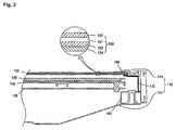
- FIG. 2 shows the construction of a plasma display apparatus comprising a glass filter in the related art.
- the glass filter of the prior art plasma display apparatus comprises a transparent glass substrate 151 spaced apart from the plasma display panel 120 at a predetermined distance, an anti-reflection film 152 formed on the transparent glass substrate 151, a color-dye film 153 adjacent to the transparent glass substrate 151, for shielding NIR and controlling color, and an EMI-shielding film 154 for shielding EMI.
- the transparent glass substrate 151 serves as a base forming the filter and protects the plasma display panel from external shock.
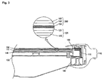
- FIG. 3 shows the construction of a plasma display apparatus comprising a film filter in the related art.
- the prior art film filter 350 comprises an EMI-shielding film 154, a color-dye film 153 and an anti-reflection film 152.
- the prior art film filter is directly attached to a front substrate 121 of the plasma display panel by means of a lamination method, etc.
- the EMI-shielding film 154 of the glass filter and the film filter in the related art is formed using a black layer of a mesh type in order to improve the contrast ratio.
- the black layer functions to lower the transmittance of light, which is incident on the filter from the outside and thus to lower light reflecting from the surface of the plasma display. Therefore, the contrast ratio of the plasma display apparatus can be improved.
- the black layer included in the glass filter or the film filter of the related art shields light generated when the plasma display panel is driven. That is, the black layer included in the filter lowers the aspect ratio and reduces brightness.
- an object of the embodiment of the present invention is to solve at least the problems and disadvantages of the background art.
- a plasma display apparatus comprises a plasma display panel radiating light, and a filter comprising a concentrating layer disposed over the plasma display panel, for concentrating the light, and a light-transmitting layer disposed on the concentrating layer and comprising a plurality of apertures through which the concentrated light passes.
- a filter according to an aspect of the present invention comprises a concentrating layer disposed over the plasma display panel, for concentrating the light, and a light-transmitting layer disposed on the concentrating layer and comprising a plurality of apertures through which the concentrated light passes formed therein.
- FIG. 1 schematically shows the construction of a plasma display apparatus in the related art
- FIG. 2 shows the construction of a plasma display apparatus comprising a glass filter in the related art
- FIG. 3 shows the construction of a plasma display apparatus comprising a film filter in the related art
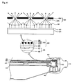
- FIG. 4 shows the construction of a plasma display apparatus comprising a film filter according to an embodiment of the present invention.
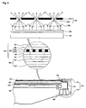
- FIG. 5 shows the construction of a plasma display apparatus comprising a glass filter according to an embodiment of the present invention.
- a plasma display apparatus comprises a plasma display panel radiating light, and a filter comprising a concentrating layer disposed over the plasma display panel, for concentrating the light, and a light-transmitting layer disposed on the concentrating layer and comprising a plurality of apertures through which the concentrated light passes.
- the light-transmitting layer may be a conductive mesh layer.
- the conductive mesh layer may be made of a black conductive material.
- the conductive mesh layer may be grounded.
- the conductive mesh layer may be a copper mesh layer.
- the copper mesh layer may comprise a surface blackened by means of oxidization.
- the light-transmitting layer may comprise a surface blackened by means of oxidization.
- the concentrating layer may be a micro lens array comprising a plurality of unit lenses.
- Each of the unit lenses may comprise a convex shape in the direction to the plasma display panel.
- the focus of one of the unit lenses may be formed in one aperture.
- the filter may be either of a glass filter or a film filter.
- a filter according to an aspect of the present invention comprises a concentrating layer disposed over the plasma display panel, for concentrating the light, and a light-transmitting layer disposed on the concentrating layer and having a plurality of apertures through which the concentrated light passes.
- the light-transmitting layer may be a conductive mesh layer.
- the conductive mesh layer may be made of a black conductive material.
- the conductive mesh layer may be a copper mesh layer.
- the copper mesh layer may comprise a surface blackened by means of oxidization.
- the light-transmitting layer may comprise a surface blackened by means of oxidization.
- the concentrating layer may be a micro lens array comprising a plurality of unit lenses.
- Each of the unit lenses may comprise a convex shape in an opposite direction to the light-transmitting layer.
- the focus of one of the unit lenses may be formed in the one aperture.
- FIG. 4 shows the construction of a plasma display apparatus comprising a film filter according to an embodiment of the present invention.
- the plasma display apparatus of the present invention comprises a casing 410 comprising a front cabinet 411 and a back cover 412, which decide an external form, a plasma display panel 420 mounted within a casing, a driving circuit substrate 430 for driving the plasma display panel 420, a heat dissipation sheet 440 coupled to the driving circuit substrate 430, for dissipating heat to the outside, a film filter 400 comprising a concentrating layer 402 that enhances the contrast ratio and brightness, a filter supporter 470 that supports the film filter 400 and is electrically connected to the back cover 412, and a module supporter 480 that supports the driving circuit substrate 430 and the plasma display panel 420.
- the film filter 400 of the present invention comprises a NIR-shielding film 401 that shields NIR, an EMI-shielding film 403 that shields EMI, an anti-reflection film 404 that prevents the reflection of incident light, and the concentrating layer 402 for enhancing the contrast ratio and brightness.
- the EMI-shielding film 403 of the film filter 400 is a black layer 403a of a mesh type, which comprises a plurality of apertures 403b.
- the black layer 403a comprises a copper mesh whose surface is oxidized and then blackened. Therefore, the black layer 403a has a good electrical conductivity while having a black color. Therefore, the black layer 403a reduces light reflected from the surface of the plasma display panel, thus improving the contrast ratio of the plasma display apparatus. Furthermore the black layer 403a is grounded and therefore shields EMI generated by the plasma display panel.
- the concentrating layer 402 is disposed over the plasma display panel 420 that radiates light corresponding to an image.
- the black layer 403a that serves as the EMI-shielding film 403 is disposed on the concentrating layer 402.
- the concentrating layer 402 can be a micro lens array.
- the micro lens array used as the concentrating layer 402 comprises a plurality of unit lenses.
- Each of the unit lenses comprises a convex shape in the direction to a front substrate 421. If each unit lens comprises a convex shape in the direction to the front substrate 421, light passing through the unit lens is concentrated into a focus of the unit lens. If light radiated from the front substrate 421 of the plasma display panel to the outside passes through the micro lens array (i.e., the concentrating layer 402), it is concentrated on a focus of the micro lens array.
- the focus of the unit lens of the micro lens array is located at the center of one of the apertures 403b of the black layer 403a.
- Light that has passed through the unit lens of the micro lens array 402 is concentrated at the center of the aperture 403b where the focus of the unit lens is located, and is then radiated to the outside.
- the brightness of the plasma display apparatus can be enhanced.
- FIG. 5 shows the construction of a plasma display apparatus comprising a glass filter according to an embodiment of the present invention.
- the plasma display apparatus of the present invention comprises a casing 510 comprising a front cabinet 511 and a back cover 512, which decide an external form, a plasma display panel 520 mounted within a casing, a driving circuit substrate 530 for driving the plasma display panel 520, a heat dissipation sheet 540 coupled to the driving circuit substrate 530, for dissipating heat to the outside, a glass filter 500 comprising a concentrating layer 502 that enhances the contrast ratio and brightness, a filter supporter 570 that supports the glass filter 500 and is electrically connected to the back cover 512, and a module supporter 580 that supports the driving circuit substrate 530 and the plasma display panel 520.
- the glass filter 500 of the present invention comprises a NIR-shielding film 501, the concentrating layer 502 for improving the contrast ratio and brightness, an EMI-shielding film 503, a glass substrate 505 and an anti-reflection film 504.
- the NIR-shielding film 501, the EMI-shielding film 503 and the anti-reflection film 504 have the same functions as those of the NIR-shielding film 501, the EMI-shielding film 503 and the anti-reflection film 504 included in the film filter. Therefore, detailed description thereof will be omitted.
- the glass substrate 505 serves as a base for forming the NIR-shielding film 501, the concentrating layer 502, the EMI-shielding film 503 and the anti-reflection film 504, and protects the plasma display panel 520.
- the EMI-shielding film 503 of the glass filter 500 is a black layer 503a of a mesh type, which comprises apertures 503b.
- the black layer 503a comprises a copper mesh whose surface is oxidized and then blackened. Therefore, the black layer 503a can improve the contrast ratio of the plasma display apparatus. Furthermore, the black layer 503a is grounded and shields EMI generated by the plasma display panel.
- the concentrating layer 502 is disposed over the plasma display panel.
- the black layer 503a serving as the EMI-shielding film 503 is disposed on the concentrating layer 502.
- the concentrating layer 502 is a micro lens array.
- the micro lens array used as the concentrating layer 502 comprises a plurality of unit lenses that have a convex shape in the direction to the front substrate 521. If each of the unit lenses comprises a convex shape in the direction to the front substrate 521, light that has radiated from the plasma display panel 520 and then passes through the unit lens gathers at a focus of the unit lens.
- the focus of the unit lens of the micro lens array is located at the center of one of the apertures 503b of the black layer 503a.
- Light that has passed through the unit lens of the micro lens array 502 is concentrated at the center of the aperture 503b where the focus of the unit lens is located, and is then radiated to the outside.
- the brightness of the plasma display apparatus can be enhanced.
Abstract
Description
- This document relates to a plasma display apparatus comprising a filter.
- In general, a plasma display panel consists of a front substrate and a rear substrate made of soda-lime glass. Barrier ribs formed between the front substrate and the rear substrate partition discharge cells. An inert gas injected into the discharge cells, such as helium-xeon (He-Xe) or helium-neon (He-Ne) generates a discharge with a high frequency voltage. When a discharge is generated, vacuum ultraviolet rays are generated. Vacuum ultraviolet rays light-emit phosphors formed between the barrier ribs, implementing images.
- FIG. 1 schematically shows the construction of a plasma display apparatus in the related art. As shown in FIG. 1, the related art plasma display apparatus comprises a
casing 110 comprising afront cabinet 111 and aback cover 112, aplasma display panel 120 mounted in thecasing 110, adriving apparatus 130 for driving theplasma display panel 120, and aframe 140 coupled to thedriving apparatus 130, for dissipating heat generating when the plasma display panel is driven and supporting the plasma display panel. - The related art plasma display apparatus further comprises a
filter 150 whose film is attached to a transparent glass substrate (not shown), afilter spring gasket 160 and afilter supporter 170, which support thefilter 150 and are electrically connected to theback cover 112, and amodule supporter 180 for supporting thedriving apparatus 130 and theplasma display panel 120. - The related art plasma display apparatus implements images using a driving pulse of a high voltage and a high frequency for the purpose of a plasma discharge. Therefore, there is a problem in that a great amount of Electromagnetic Interference (hereinafter referred to as "EMI"), which is generated by the driving pulse, is dissipated through a front glass. More particularly, an amount of EMI generated by the plasma display apparatus is greater than that generated by a Cathode Ray Tube (CRT) or a Liquid Crystal Display (LCD).
- The prior art plasma display apparatus radiates Near Infrared Rays (hereinafter referred to as "NIR") generated by an inert gas such as Ne or Xe. The NIR generated from the prior art plasma display apparatus is problematic in that it causes malfunction because it is very close to a wavelength of NIR output from a remote controller of home appliances. Furthermore, a problem arises because a user may feel dazzling due to external light as in CRT or LCD. There is also a problem, such as a low contrast ratio, which is one of picture quality characteristics of other display apparatuses.
- Therefore, the prior art plasma display apparatus comprises a filter capable of reducing or obviating EMI or NIR. The filter of the plasma display apparatus can be classified into a glass filter and a film filter depending on its structure.
- FIG. 2 shows the construction of a plasma display apparatus comprising a glass filter in the related art. As shown in FIG. 2, the glass filter of the prior art plasma display apparatus comprises a
transparent glass substrate 151 spaced apart from theplasma display panel 120 at a predetermined distance, ananti-reflection film 152 formed on thetransparent glass substrate 151, a color-dye film 153 adjacent to thetransparent glass substrate 151, for shielding NIR and controlling color, and an EMI-shielding film 154 for shielding EMI. Thetransparent glass substrate 151 serves as a base forming the filter and protects the plasma display panel from external shock. - FIG. 3 shows the construction of a plasma display apparatus comprising a film filter in the related art. As shown in FIG. 3, the prior
art film filter 350 comprises an EMI-shielding film 154, a color-dye film 153 and ananti-reflection film 152. The prior art film filter is directly attached to afront substrate 121 of the plasma display panel by means of a lamination method, etc. - The EMI-
shielding film 154 of the glass filter and the film filter in the related art is formed using a black layer of a mesh type in order to improve the contrast ratio. The black layer functions to lower the transmittance of light, which is incident on the filter from the outside and thus to lower light reflecting from the surface of the plasma display. Therefore, the contrast ratio of the plasma display apparatus can be improved. However, the black layer included in the glass filter or the film filter of the related art shields light generated when the plasma display panel is driven. That is, the black layer included in the filter lowers the aspect ratio and reduces brightness. - Accordingly, an object of the embodiment of the present invention is to solve at least the problems and disadvantages of the background art.
- It is an object of the embodiment of the present invention to provide a plasma display apparatus comprising a filter, in which it can reduce a reduction in brightness and improve the contrast ratio.
- A plasma display apparatus according to an aspect of the present invention comprises a plasma display panel radiating light, and a filter comprising a concentrating layer disposed over the plasma display panel, for concentrating the light, and a light-transmitting layer disposed on the concentrating layer and comprising a plurality of apertures through which the concentrated light passes.
- A filter according to an aspect of the present invention comprises a concentrating layer disposed over the plasma display panel, for concentrating the light, and a light-transmitting layer disposed on the concentrating layer and comprising a plurality of apertures through which the concentrated light passes formed therein.
- It is thus possible to improve brightness and the contrast ratio and shield EMI.
- The embodiment of the invention will be described in detail with reference to the following drawings in which like numerals refer to like elements.
- FIG. 1 schematically shows the construction of a plasma display apparatus in the related art;
- FIG. 2 shows the construction of a plasma display apparatus comprising a glass filter in the related art;
- FIG. 3 shows the construction of a plasma display apparatus comprising a film filter in the related art;
- FIG. 4 shows the construction of a plasma display apparatus comprising a film filter according to an embodiment of the present invention; and
- FIG. 5 shows the construction of a plasma display apparatus comprising a glass filter according to an embodiment of the present invention.
- Embodiments of the present invention will be described in a more detailed manner with reference to the drawings.
- A plasma display apparatus according to an aspect of the present invention comprises a plasma display panel radiating light, and a filter comprising a concentrating layer disposed over the plasma display panel, for concentrating the light, and a light-transmitting layer disposed on the concentrating layer and comprising a plurality of apertures through which the concentrated light passes.
- The light-transmitting layer may be a conductive mesh layer.
- The conductive mesh layer may be made of a black conductive material.
- The conductive mesh layer may be grounded.
- The conductive mesh layer may be a copper mesh layer.
- The copper mesh layer may comprise a surface blackened by means of oxidization.
- The light-transmitting layer may comprise a surface blackened by means of oxidization.
- The concentrating layer may be a micro lens array comprising a plurality of unit lenses.
- Each of the unit lenses may comprise a convex shape in the direction to the plasma display panel.
- The focus of one of the unit lenses may be formed in one aperture.
- The filter may be either of a glass filter or a film filter.
- A filter according to an aspect of the present invention comprises a concentrating layer disposed over the plasma display panel, for concentrating the light, and a light-transmitting layer disposed on the concentrating layer and having a plurality of apertures through which the concentrated light passes.
- The light-transmitting layer may be a conductive mesh layer.
- The conductive mesh layer may be made of a black conductive material.
- The conductive mesh layer may be a copper mesh layer.
- The copper mesh layer may comprise a surface blackened by means of oxidization.
- The light-transmitting layer may comprise a surface blackened by means of oxidization.
- The concentrating layer may be a micro lens array comprising a plurality of unit lenses.
- Each of the unit lenses may comprise a convex shape in an opposite direction to the light-transmitting layer.
- The focus of one of the unit lenses may be formed in the one aperture.
- It is thus possible to improve brightness and the contrast ratio and shield EMI.
- Detailed embodiments of the present invention will be described below with reference to the accompanying drawings.
- FIG. 4 shows the construction of a plasma display apparatus comprising a film filter according to an embodiment of the present invention. As shown in FIG. 4, the plasma display apparatus of the present invention comprises a
casing 410 comprising afront cabinet 411 and aback cover 412, which decide an external form, aplasma display panel 420 mounted within a casing, a drivingcircuit substrate 430 for driving theplasma display panel 420, aheat dissipation sheet 440 coupled to thedriving circuit substrate 430, for dissipating heat to the outside, afilm filter 400 comprising a concentratinglayer 402 that enhances the contrast ratio and brightness, afilter supporter 470 that supports thefilm filter 400 and is electrically connected to theback cover 412, and amodule supporter 480 that supports the drivingcircuit substrate 430 and theplasma display panel 420. - The
film filter 400 of the present invention comprises a NIR-shieldingfilm 401 that shields NIR, an EMI-shieldingfilm 403 that shields EMI, ananti-reflection film 404 that prevents the reflection of incident light, and the concentratinglayer 402 for enhancing the contrast ratio and brightness. - The EMI-shielding
film 403 of thefilm filter 400 is ablack layer 403a of a mesh type, which comprises a plurality ofapertures 403b. Theblack layer 403a comprises a copper mesh whose surface is oxidized and then blackened. Therefore, theblack layer 403a has a good electrical conductivity while having a black color. Therefore, theblack layer 403a reduces light reflected from the surface of the plasma display panel, thus improving the contrast ratio of the plasma display apparatus. Furthermore theblack layer 403a is grounded and therefore shields EMI generated by the plasma display panel. - The concentrating
layer 402 is disposed over theplasma display panel 420 that radiates light corresponding to an image. Theblack layer 403a that serves as the EMI-shieldingfilm 403 is disposed on the concentratinglayer 402. The concentratinglayer 402 can be a micro lens array. - The micro lens array used as the concentrating
layer 402 comprises a plurality of unit lenses. Each of the unit lenses comprises a convex shape in the direction to afront substrate 421. If each unit lens comprises a convex shape in the direction to thefront substrate 421, light passing through the unit lens is concentrated into a focus of the unit lens. If light radiated from thefront substrate 421 of the plasma display panel to the outside passes through the micro lens array (i.e., the concentrating layer 402), it is concentrated on a focus of the micro lens array. - The focus of the unit lens of the micro lens array is located at the center of one of the
apertures 403b of theblack layer 403a. Light that has passed through the unit lens of themicro lens array 402 is concentrated at the center of theaperture 403b where the focus of the unit lens is located, and is then radiated to the outside. - Since light is concentrated at the center of the
aperture 403b by means of the micro lens array of the concentratinglayer 403, the brightness of the plasma display apparatus can be enhanced. - Furthermore, most of light, which is incident on the
front substrate 421 of theplasma display panel 420 from the outside, is absorbed by theblack layer 403a. Light that is incident through theaperture 403b of theblack layer 403a is absorbed by theblack layer 403a again although it is reflected from thefront substrate 421 of the plasma display panel. As a result, since an amount of light reflected from the front substrate of the plasma display panel is reduced, the contrast ratio can be improved. - FIG. 5 shows the construction of a plasma display apparatus comprising a glass filter according to an embodiment of the present invention. As shown in FIG. 5, the plasma display apparatus of the present invention comprises a
casing 510 comprising afront cabinet 511 and aback cover 512, which decide an external form, aplasma display panel 520 mounted within a casing, a drivingcircuit substrate 530 for driving theplasma display panel 520, aheat dissipation sheet 540 coupled to thedriving circuit substrate 530, for dissipating heat to the outside, aglass filter 500 comprising a concentratinglayer 502 that enhances the contrast ratio and brightness, afilter supporter 570 that supports theglass filter 500 and is electrically connected to theback cover 512, and amodule supporter 580 that supports the drivingcircuit substrate 530 and theplasma display panel 520. - The
glass filter 500 of the present invention comprises a NIR-shieldingfilm 501, the concentratinglayer 502 for improving the contrast ratio and brightness, an EMI-shieldingfilm 503, aglass substrate 505 and ananti-reflection film 504. - The NIR-shielding
film 501, the EMI-shieldingfilm 503 and theanti-reflection film 504 have the same functions as those of the NIR-shieldingfilm 501, the EMI-shieldingfilm 503 and theanti-reflection film 504 included in the film filter. Therefore, detailed description thereof will be omitted. - The
glass substrate 505 serves as a base for forming the NIR-shieldingfilm 501, the concentratinglayer 502, the EMI-shieldingfilm 503 and theanti-reflection film 504, and protects theplasma display panel 520. - The EMI-shielding
film 503 of theglass filter 500 is ablack layer 503a of a mesh type, which comprisesapertures 503b. Theblack layer 503a comprises a copper mesh whose surface is oxidized and then blackened. Therefore, theblack layer 503a can improve the contrast ratio of the plasma display apparatus. Furthermore, theblack layer 503a is grounded and shields EMI generated by the plasma display panel. - The concentrating
layer 502 is disposed over the plasma display panel. Theblack layer 503a serving as the EMI-shieldingfilm 503 is disposed on the concentratinglayer 502. The concentratinglayer 502 is a micro lens array. - The micro lens array used as the concentrating
layer 502 comprises a plurality of unit lenses that have a convex shape in the direction to thefront substrate 521. If each of the unit lenses comprises a convex shape in the direction to thefront substrate 521, light that has radiated from theplasma display panel 520 and then passes through the unit lens gathers at a focus of the unit lens. - The focus of the unit lens of the micro lens array is located at the center of one of the
apertures 503b of theblack layer 503a. Light that has passed through the unit lens of themicro lens array 502 is concentrated at the center of theaperture 503b where the focus of the unit lens is located, and is then radiated to the outside. - Since light is concentrated at the center of the
aperture 503b by means of the micro lens array of the concentratinglayer 503, the brightness of the plasma display apparatus can be enhanced. - Furthermore, most of light, which is incident on the
front substrate 521 of theplasma display panel 520 from the outside, is absorbed by theblack layer 503a. Light that is incident through theaperture 503b of theblack layer 503a is absorbed by theblack layer 503a again although it is reflected from thefront substrate 521 of the plasma display panel. As a result, since an amount of light reflected from the front substrate of the plasma display panel is reduced, the contrast ratio can be improved. - The invention being thus described, it will be obvious that the same may be varied in many ways. Such variations are not to be regarded as a departure from the spirit and scope of the invention, and all such modifications as would be obvious to one skilled in the art are intended to be included within the scope of the following claims.
Claims (20)
- A plasma display apparatus comprising:a plasma display panel radiating light; anda filter comprising a concentrating layer disposed over the plasma display panel, for concentrating the light, and a light-transmitting layer disposed on the concentrating layer and comprising a plurality of apertures through which the concentrated light passes.
- The plasma display apparatus as claimed in claim 1, wherein the light-transmitting layer is a conductive mesh layer.
- The plasma display apparatus as claimed in claim 2, wherein the conductive mesh layer is made of a black conductive material.
- The plasma display apparatus as claimed in claim 2, wherein the conductive mesh layer is grounded.
- The plasma display apparatus as claimed in claim 2, wherein the conductive mesh layer is a copper mesh layer.
- The plasma display apparatus as claimed in claim 5, wherein the copper mesh layer comprises a surface blackened by means of oxidization.
- The plasma display apparatus as claimed in claim 1, wherein the light-transmitting layer comprises a surface blackened by means of oxidization.
- The plasma display apparatus as claimed in claim 1, wherein the concentrating layer is a micro lens array comprising a plurality of unit lenses.
- The plasma display apparatus as claimed in claim 8, wherein each of the unit lenses comprises a convex shape in the direction to the plasma display panel.
- The plasma display apparatus as claimed in claim 8, wherein the focus of one of the unit lenses is formed in one aperture.
- The plasma display apparatus as claimed in claim 1, wherein the filter is either of a glass filter or a film filter.
- A filter disposed over a plasma display panel radiating light, comprising:a concentrating layer disposed over the plasma display panel, for concentrating the light; anda light-transmitting layer disposed on the concentrating layer and comprising a plurality of apertures through which the concentrated light passes.
- The filter as claimed in claim 12, wherein the light-transmitting layer is a conductive mesh layer.
- The filter as claimed in claim 13, wherein the conductive mesh layer is made of a black conductive material.
- The filter as claimed in claim 13, wherein the conductive mesh layer is a copper mesh layer.
- The filter as claimed in claim 15, wherein the copper mesh layer comprises a surface blackened by means of oxidization.
- The filter as claimed in claim 12, wherein the light-transmitting layer comprises a surface blackened by means of oxidization.
- The filter as claimed in claim 12, wherein the concentrating layer is a micro lens array comprising a plurality of unit lenses.
- The filter as claimed in claim 8, wherein each of the unit lenses has a convex shape in an opposite direction to the light-transmitting layer.
- The filter as claimed in claim 18, wherein the focus of one of the unit lenses is formed in the one aperture.
Applications Claiming Priority (1)
| Application Number | Priority Date | Filing Date | Title |
|---|---|---|---|
| KR1020040103844A KR100738814B1 (en) | 2004-12-09 | 2004-12-09 | Filter for Plasma Display Apparatus and Plasma Display Apparatus comprising the Filter |
Publications (2)
| Publication Number | Publication Date |
|---|---|
| EP1670024A2 true EP1670024A2 (en) | 2006-06-14 |
| EP1670024A3 EP1670024A3 (en) | 2009-05-27 |
Family
ID=36088249
Family Applications (1)
| Application Number | Title | Priority Date | Filing Date |
|---|---|---|---|
| EP05292617A Withdrawn EP1670024A3 (en) | 2004-12-09 | 2005-12-08 | Plasma display apparatus comprising filter |
Country Status (5)
| Country | Link |
|---|---|
| US (1) | US20060125366A1 (en) |
| EP (1) | EP1670024A3 (en) |
| JP (1) | JP2006163422A (en) |
| KR (1) | KR100738814B1 (en) |
| CN (1) | CN1787044A (en) |
Cited By (3)
| Publication number | Priority date | Publication date | Assignee | Title |
|---|---|---|---|---|
| WO2007067572A1 (en) * | 2005-12-07 | 2007-06-14 | Bright View Technologies, Inc. | Optically transparent electromagnetic interference (emi) shields for direct-view displays |
| EP1868223A3 (en) * | 2006-06-15 | 2008-12-10 | Samsung Electronics Co., Ltd. | Display panel |
| US7502169B2 (en) | 2005-12-07 | 2009-03-10 | Bright View Technologies, Inc. | Contrast enhancement films for direct-view displays and fabrication methods therefor |
Families Citing this family (8)
| Publication number | Priority date | Publication date | Assignee | Title |
|---|---|---|---|---|
| KR20060042478A (en) * | 2004-11-09 | 2006-05-15 | 엘지전자 주식회사 | Front filter of plasma display panel with microlens array |
| KR100783645B1 (en) * | 2006-11-06 | 2007-12-07 | 엘지전자 주식회사 | Plasma display device |
| WO2008020664A1 (en) * | 2006-08-18 | 2008-02-21 | Lg Electronics Inc. | Filter and plasma display device thereof |
| JP5022666B2 (en) * | 2006-10-23 | 2012-09-12 | 株式会社日立製作所 | Plasma display device |
| KR100870290B1 (en) * | 2006-10-31 | 2008-11-25 | 삼성정밀화학 주식회사 | Visibility enhancement film, display filter and display apparatus using the same |
| KR100775837B1 (en) * | 2006-11-06 | 2007-11-13 | 엘지전자 주식회사 | Filter and plasma display device thereof |
| JP2012083557A (en) * | 2010-10-12 | 2012-04-26 | Asahi Glass Co Ltd | Plasma display device and filter substrate for plasma display device |
| KR102567498B1 (en) * | 2018-09-13 | 2023-08-16 | 삼성디스플레이 주식회사 | Cover window and display apparatus having the same |
Citations (5)
| Publication number | Priority date | Publication date | Assignee | Title |
|---|---|---|---|---|
| JPH10282309A (en) * | 1997-04-04 | 1998-10-23 | Toppan Printing Co Ltd | Lens sheet with electromagnetic shield function, and its manufacture |
| JP2001154597A (en) * | 1999-11-25 | 2001-06-08 | Toppan Printing Co Ltd | Front plate of plasma display panel |
| EP1209715A2 (en) * | 2000-11-21 | 2002-05-29 | GRUNDIG Aktiengesellschaft | Front panel for shielding a flat plasma display screen |
| US20040222003A1 (en) * | 2003-04-10 | 2004-11-11 | Lg Electronics Inc. | Electromagnetic interference shielding filter manufacturing method thereof |
| EP1655759A2 (en) * | 2004-11-09 | 2006-05-10 | LG Electronics Inc. | Front filter of display panel and fabrication method thereof |
Family Cites Families (12)
| Publication number | Priority date | Publication date | Assignee | Title |
|---|---|---|---|---|
| JPH0589850A (en) * | 1991-09-27 | 1993-04-09 | Canon Inc | Flat plate type light emitting tube |
| DE69631095T2 (en) * | 1995-07-06 | 2004-08-26 | Dai Nippon Printing Co., Ltd. | Holographic color filter and its manufacturing process |
| JP3586326B2 (en) * | 1995-10-31 | 2004-11-10 | ソニー株式会社 | Transmissive display |
| JPH11119675A (en) * | 1997-10-16 | 1999-04-30 | Dainippon Printing Co Ltd | Production of electromagnetic shielding plate |
| JPH11260269A (en) * | 1998-03-11 | 1999-09-24 | Omron Corp | Plasma display device and plasma display substrate thereof |
| JP3464155B2 (en) * | 1998-09-30 | 2003-11-05 | 三菱電機株式会社 | Display device and method of manufacturing the same |
| KR20010041206A (en) * | 1998-12-24 | 2001-05-15 | 요트.게.아. 롤페즈 | Image display panel |
| JP2001305315A (en) * | 2000-02-14 | 2001-10-31 | Fuji Photo Film Co Ltd | Light diffusing plate, liquid crystal display device and rear projector device |
| JP2002123182A (en) * | 2000-08-10 | 2002-04-26 | Nisshinbo Ind Inc | Front plate for plasma display panel and its manufacturing method |
| JP2004206076A (en) * | 2002-12-10 | 2004-07-22 | Pioneer Electronic Corp | Flat display device |
| KR100511789B1 (en) * | 2003-04-10 | 2005-09-02 | 엘지전자 주식회사 | Front-filter |
| KR100665026B1 (en) * | 2004-05-17 | 2007-01-09 | 삼성코닝 주식회사 | Filter for display device, display device employing the same and method for fabricating the same |
-
2004
- 2004-12-09 KR KR1020040103844A patent/KR100738814B1/en not_active IP Right Cessation
-
2005
- 2005-12-08 EP EP05292617A patent/EP1670024A3/en not_active Withdrawn
- 2005-12-08 JP JP2005354549A patent/JP2006163422A/en active Pending
- 2005-12-08 US US11/296,427 patent/US20060125366A1/en not_active Abandoned
- 2005-12-09 CN CNA2005101297919A patent/CN1787044A/en active Pending
Patent Citations (5)
| Publication number | Priority date | Publication date | Assignee | Title |
|---|---|---|---|---|
| JPH10282309A (en) * | 1997-04-04 | 1998-10-23 | Toppan Printing Co Ltd | Lens sheet with electromagnetic shield function, and its manufacture |
| JP2001154597A (en) * | 1999-11-25 | 2001-06-08 | Toppan Printing Co Ltd | Front plate of plasma display panel |
| EP1209715A2 (en) * | 2000-11-21 | 2002-05-29 | GRUNDIG Aktiengesellschaft | Front panel for shielding a flat plasma display screen |
| US20040222003A1 (en) * | 2003-04-10 | 2004-11-11 | Lg Electronics Inc. | Electromagnetic interference shielding filter manufacturing method thereof |
| EP1655759A2 (en) * | 2004-11-09 | 2006-05-10 | LG Electronics Inc. | Front filter of display panel and fabrication method thereof |
Cited By (5)
| Publication number | Priority date | Publication date | Assignee | Title |
|---|---|---|---|---|
| WO2007067572A1 (en) * | 2005-12-07 | 2007-06-14 | Bright View Technologies, Inc. | Optically transparent electromagnetic interference (emi) shields for direct-view displays |
| US7420742B2 (en) | 2005-12-07 | 2008-09-02 | Bright View Technologies, Inc. | Optically transparent electromagnetic interference (EMI) shields for direct-view displays |
| US7502169B2 (en) | 2005-12-07 | 2009-03-10 | Bright View Technologies, Inc. | Contrast enhancement films for direct-view displays and fabrication methods therefor |
| EP1868223A3 (en) * | 2006-06-15 | 2008-12-10 | Samsung Electronics Co., Ltd. | Display panel |
| US8058804B2 (en) | 2006-06-15 | 2011-11-15 | Samsung Electronics Co., Ltd. | Display device having light blocking members |
Also Published As
| Publication number | Publication date |
|---|---|
| KR20060065110A (en) | 2006-06-14 |
| KR100738814B1 (en) | 2007-07-12 |
| US20060125366A1 (en) | 2006-06-15 |
| CN1787044A (en) | 2006-06-14 |
| EP1670024A3 (en) | 2009-05-27 |
| JP2006163422A (en) | 2006-06-22 |
Similar Documents
| Publication | Publication Date | Title |
|---|---|---|
| EP1670024A2 (en) | Plasma display apparatus comprising filter | |
| CN100523917C (en) | Liquid crystal display device with electromagnetic wave screening element | |
| KR100546261B1 (en) | Display Panel Moudle | |
| JP2008158530A (en) | External light shielding layer for display filter, filter for display apparatus, and display apparatus | |
| US20040090182A1 (en) | Plasma display panel | |
| KR100509764B1 (en) | Electromagnetic wave shilding filter and method for fabricating the same | |
| KR20040085765A (en) | Front-filter of film type using plasma display panel | |
| JP4271163B2 (en) | Plasma display device and film filter thereof | |
| KR20040085762A (en) | Method for fabricating electromagnetic wave shilding film and display panel module using the same, and fabricating method tererof | |
| KR100441529B1 (en) | Display device using plasma display panel | |
| JP2005070661A (en) | Panel type display device | |
| KR20040095767A (en) | Display panel module with front-filter and fabricating method tererof | |
| US20070190860A1 (en) | Plasma display apparatus | |
| KR100579329B1 (en) | Plasma Display Apparatus | |
| KR100585530B1 (en) | Plasma Display Equipment | |
| KR100709879B1 (en) | Film filter of a plasma display panel | |
| KR20040088700A (en) | Front-filter and display panel module using the same | |
| KR100580680B1 (en) | earth structure of plasma display device | |
| KR100509598B1 (en) | Plasma display apparatus | |
| KR100866875B1 (en) | Plasma display apparatus | |
| KR101052738B1 (en) | Optical member for display device, method for manufacturing same and filter and display device for display device including same | |
| US8369106B2 (en) | Plasma display apparatus to reduce EMI emission | |
| KR101072429B1 (en) | Optical member for display apparatus, method for fabricating the same, filter for display device and display device employing the same | |
| KR100747217B1 (en) | The Filter for Plasma Display Apparatus and Plasma Display Apparatus Containing the Same | |
| KR20040090076A (en) | Display panel module and fabricating method tererof |
Legal Events
| Date | Code | Title | Description |
|---|---|---|---|
| PUAI | Public reference made under article 153(3) epc to a published international application that has entered the european phase |
Free format text: ORIGINAL CODE: 0009012 |
|
| 17P | Request for examination filed |
Effective date: 20051216 |
|
| AK | Designated contracting states |
Kind code of ref document: A2 Designated state(s): AT BE BG CH CY CZ DE DK EE ES FI FR GB GR HU IE IS IT LI LT LU LV MC NL PL PT RO SE SI SK TR |
|
| AX | Request for extension of the european patent |
Extension state: AL BA HR MK YU |
|
| PUAL | Search report despatched |
Free format text: ORIGINAL CODE: 0009013 |
|
| AK | Designated contracting states |
Kind code of ref document: A3 Designated state(s): AT BE BG CH CY CZ DE DK EE ES FI FR GB GR HU IE IS IT LI LT LU LV MC NL PL PT RO SE SI SK TR |
|
| AX | Request for extension of the european patent |
Extension state: AL BA HR MK YU |
|
| RIC1 | Information provided on ipc code assigned before grant |
Ipc: H01J 17/49 20060101ALI20090421BHEP Ipc: H01J 17/16 20060101AFI20060406BHEP |
|
| AKX | Designation fees paid | ||
| REG | Reference to a national code |
Ref country code: DE Ref legal event code: 8566 |
|
| STAA | Information on the status of an ep patent application or granted ep patent |
Free format text: STATUS: THE APPLICATION IS DEEMED TO BE WITHDRAWN |
|
| 18D | Application deemed to be withdrawn |
Effective date: 20091128 |