EP1677153B1 - Lithographic apparatus and device manufacturing method - Google Patents
Lithographic apparatus and device manufacturing method Download PDFInfo
- Publication number
- EP1677153B1 EP1677153B1 EP20050257739 EP05257739A EP1677153B1 EP 1677153 B1 EP1677153 B1 EP 1677153B1 EP 20050257739 EP20050257739 EP 20050257739 EP 05257739 A EP05257739 A EP 05257739A EP 1677153 B1 EP1677153 B1 EP 1677153B1
- Authority
- EP
- European Patent Office
- Prior art keywords
- substrate
- layer
- final element
- liquid
- projection system
- Prior art date
- Legal status (The legal status is an assumption and is not a legal conclusion. Google has not performed a legal analysis and makes no representation as to the accuracy of the status listed.)
- Expired - Fee Related
Links
Images


Classifications
-
- G—PHYSICS
- G03—PHOTOGRAPHY; CINEMATOGRAPHY; ANALOGOUS TECHNIQUES USING WAVES OTHER THAN OPTICAL WAVES; ELECTROGRAPHY; HOLOGRAPHY
- G03F—PHOTOMECHANICAL PRODUCTION OF TEXTURED OR PATTERNED SURFACES, e.g. FOR PRINTING, FOR PROCESSING OF SEMICONDUCTOR DEVICES; MATERIALS THEREFOR; ORIGINALS THEREFOR; APPARATUS SPECIALLY ADAPTED THEREFOR
- G03F7/00—Photomechanical, e.g. photolithographic, production of textured or patterned surfaces, e.g. printing surfaces; Materials therefor, e.g. comprising photoresists; Apparatus specially adapted therefor
- G03F7/70—Microphotolithographic exposure; Apparatus therefor
- G03F7/70216—Mask projection systems
- G03F7/70341—Details of immersion lithography aspects, e.g. exposure media or control of immersion liquid supply
-
- G—PHYSICS
- G03—PHOTOGRAPHY; CINEMATOGRAPHY; ANALOGOUS TECHNIQUES USING WAVES OTHER THAN OPTICAL WAVES; ELECTROGRAPHY; HOLOGRAPHY
- G03F—PHOTOMECHANICAL PRODUCTION OF TEXTURED OR PATTERNED SURFACES, e.g. FOR PRINTING, FOR PROCESSING OF SEMICONDUCTOR DEVICES; MATERIALS THEREFOR; ORIGINALS THEREFOR; APPARATUS SPECIALLY ADAPTED THEREFOR
- G03F7/00—Photomechanical, e.g. photolithographic, production of textured or patterned surfaces, e.g. printing surfaces; Materials therefor, e.g. comprising photoresists; Apparatus specially adapted therefor
- G03F7/70—Microphotolithographic exposure; Apparatus therefor
- G03F7/708—Construction of apparatus, e.g. environment aspects, hygiene aspects or materials
- G03F7/7095—Materials, e.g. materials for housing, stage or other support having particular properties, e.g. weight, strength, conductivity, thermal expansion coefficient
- G03F7/70958—Optical materials or coatings, e.g. with particular transmittance, reflectance or anti-reflection properties
Definitions
- the present invention relates to a lithographic apparatus and a method for manufacturing a device.
- a lithographic apparatus is a machine that applies a desired pattern onto a substrate, usually onto a target portion of the substrate.
- a lithographic apparatus can be used, for example, in the manufacture of integrated circuits (ICs).
- a patterning device which is alternatively referred to as a mask or a reticle, may be used to generate a circuit pattern to be formed on an individual layer of the IC.
- This pattern can be transferred onto a target portion (e.g. comprising part of, one, or several dies) on a substrate (e.g. a silicon wafer). Transfer of the pattern is typically via imaging onto a layer of radiation-sensitive material (resist) provided on the substrate.
- resist radiation-sensitive material
- a single substrate will contain a network of adjacent target portions that are successively patterned.
- lithographic apparatus include so-called steppers, in which each target portion is irradiated by exposing an entire pattern onto the target portion at one time, and so-called scanners, in which each target portion is irradiated by scanning the pattern through a radiation beam in a given direction (the "scanning"-direction) while synchronously scanning the substrate parallel or anti-parallel to this direction. It is also possible to transfer the pattern from the patterning device to the substrate by imprinting the pattern onto the substrate.
- liquid supply system to provide liquid on only a localized area of the substrate and in between the final element of the projection system and the substrate (the substrate generally has a larger surface area than the final element of the projection system).
- the substrate generally has a larger surface area than the final element of the projection system.
- liquid is supplied by at least one inlet IN onto the substrate, preferably along the direction of movement of the substrate relative to the final element, and is removed by at least one outlet OUT after having passed under the projection system. That is, as the substrate is scanned beneath the element in a -X direction, liquid is supplied at the +X side of the element and taken up at the -X side.
- Figure 2 shows the arrangement schematically in which liquid is supplied via inlet IN and is taken up on the other side of the element by outlet OUT which is connected to a low pressure source.
- the liquid is supplied along the direction of movement of the substrate relative to the final element, though this does not need to be the case.
- Figure 3 shows the arrangement schematically in which liquid is supplied via inlet IN and is taken up on the other side of the element by outlet OUT which is connected to a low pressure source.
- EP-A-1,510,871 which is citable under Article 54(3) EPC, discloses a lithographic projection system in which a final element of the projection system has a protective coating.
- WO 2004/107048 discloses a lithographic projection system in accordance with the pre-characterizing section of claim 1.
- a lithographic projection apparatus comprising:
- a device manufacturing method comprising:
- Figure 1 schematically depicts a lithographic apparatus according to one embodiment of the invention.
- the apparatus comprises:
- the illumination system may include various types of optical components, such as refractive, reflective, magnetic, electromagnetic, electrostatic or other types of optical components, or any combination thereof, for directing, shaping, or controlling radiation.
- optical components such as refractive, reflective, magnetic, electromagnetic, electrostatic or other types of optical components, or any combination thereof, for directing, shaping, or controlling radiation.
- the support structure supports, i.e. bears the weight of, the patterning device. It holds the patterning device in a manner that depends on the orientation of the patterning device, the design of the lithographic apparatus, and other conditions, such as for example whether or not the patterning device is held in a vacuum environment.
- the support structure can use mechanical, vacuum, electrostatic or other clamping techniques to hold the patterning device.
- the support structure may be a frame or a table, for example, which may be fixed or movable as required.
- the support structure may ensure that the patterning device is at a desired position, for example with respect to the projection system. Any use of the terms "reticle” or “mask” herein may be considered synonymous with the more general term "patterning device.”
- patterning device used herein should be broadly interpreted as referring to any device that can be used to impart a radiation beam with a pattern in its cross-section such as to create a pattern in a target portion of the substrate. It should be noted that the pattern imparted to the radiation beam may not exactly correspond to the desired pattern in the target portion of the substrate, for example if the pattern includes phase-shifting features or so called assist features. Generally, the pattern imparted to the radiation beam will correspond to a particular functional layer in a device being created in the target portion, such as an integrated circuit.
- the patterning device may be transmissive or reflective.
- Examples of patterning devices include masks, programmable mirror arrays, and programmable LCD panels.
- Masks are well known in lithography, and include mask types such as binary, alternating phase-shift, and attenuated phase-shift, as well as various hybrid mask types.
- An example of a programmable mirror array employs a matrix arrangement of small mirrors, each of which can be individually tilted so as to reflect an incoming radiation beam in different directions. The tilted mirrors impart a pattern in a radiation beam which is reflected by the mirror matrix.
- projection system used herein should be broadly interpreted as encompassing any type of projection system, including refractive, reflective, catadioptric, magnetic, electromagnetic and electrostatic optical systems, or any combination thereof, as appropriate for the exposure radiation being used, or for other factors such as the use of an immersion liquid or the use of a vacuum. Any use of the term “projection lens” herein may be considered as synonymous with the more general term “projection system”.
- the apparatus is of a transmissive type (e.g. employing a transmissive mask).
- the apparatus may be of a reflective type (e.g. employing a programmable mirror array of a type as referred to above, or employing a reflective mask).
- the lithographic apparatus may be of a type having two (dual stage) or more substrate tables (and/or two or more mask tables). In such "multiple stage” machines the additional tables may be used in parallel, or preparatory steps may be carried out on one or more tables while one or more other tables are being used for exposure.
- the illuminator IL receives a radiation beam from a radiation source SO.
- the source and the lithographic apparatus may be separate entities, for example when the source is an excimer laser. In such cases, the source is not considered to form part of the lithographic apparatus and the radiation beam is passed from the source SO to the illuminator IL with the aid of a beam delivery system BD comprising, for example, suitable directing mirrors and/or a beam expander. In other cases the source may be an integral part of the lithographic apparatus, for example when the source is a mercury lamp.
- the source SO and the illuminator IL, together with the beam delivery system BD if required, may be referred to as a radiation system.
- the illuminator IL may comprise an adjuster AD for adjusting the angular intensity distribution of the radiation beam.
- an adjuster AD for adjusting the angular intensity distribution of the radiation beam.
- the illuminator IL may comprise various other components, such as an integrator IN and a condenser CO.
- the illuminator may be used to condition the radiation beam, to have a desired uniformity and intensity distribution in its cross-section.
- the radiation beam B is incident on the patterning device (e.g., mask MA), which is held on the support structure (e.g., mask table MT), and is patterned by the patterning device. Having traversed the mask MA, the radiation beam B passes through the projection system PS, which focuses the beam onto a target portion C of the substrate W.
- the substrate table WT can be moved accurately, e.g. so as to position different target portions C in the path of the radiation beam B.
- the first positioner PM and another position sensor can be used to accurately position the mask MA with respect to the path of the radiation beam B, e.g. after mechanical retrieval from a mask library, or during a scan.
- movement of the mask table MT may be realized with the aid of a long-stroke module (coarse positioning) and a short-stroke module (fine positioning), which form part of the first positioner PM.
- movement of the substrate table WT may be realized using a long-stroke module and a short-stroke module, which form part of the second positioner PW.
- the mask table MT may be connected to a short-stroke actuator only, or may be fixed.
- Mask MA and substrate W may be aligned using mask alignment marks M1, M2 and substrate alignment marks P1, P2.
- the substrate alignment marks as illustrated occupy dedicated target portions, they may be located in spaces between target portions (these are known as scribe-lane alignment marks).
- the mask alignment marks may be located between the dies.
- the depicted apparatus could be used in at least one of the following modes:
- FIG. 4 A further immersion lithography solution with a localized liquid supply system is shown in Figure 4 .
- Liquid is supplied by two groove inlets IN on either side of the projection system PL and is removed by a plurality of discrete outlets OUT arranged radially outwardly of the inlets IN.
- the inlets IN and OUT can be arranged in a plate with a hole in its center and through which the projection beam is projected.
- Liquid is supplied by one groove inlet IN on one side of the projection system PL and removed by a plurality of discrete outlets OUT on the other side of the projection system PL, causing a flow of a thin film of liquid between the projection system PL and the substrate W.
- the choice of which combination of inlet IN and outlets OUT to use can depend on the direction of movement of the substrate W (the other combination of inlet IN and outlets OUT being inactive).
- Another immersion lithography solution with a localized liquid supply system solution which has been proposed is to provide the liquid supply system with a liquid confinement structure which extends along at least a part of a boundary of the space between the final element of the projection system and the substrate table.
- the liquid confinement structure is substantially stationary relative to the projection system in the XY plane though there may be some relative movement in the Z direction (in the direction of the optical axis).
- a seal is formed between the liquid confinement structure and the surface of the substrate.
- the seal is a contactless seal such as a gas seal.
- Such a system with a gas seal is disclosed in United States patent application no. US 10/705,783 (publication number US 2004/0207824 ).
- Figure 5 shows a liquid supply system comprising a liquid confinement structure (sometimes referred to as an immersion hood or showerhead) according to an embodiment of the invention.
- Figure 5 depicts an arrangement of a reservoir 10, which forms a contactless seal to the substrate around the image field of the projection system so that liquid is confined to fill a space between the substrate's primary surface, which faces the projection system PL, and the final element (e.g. an 'ab gleichplatte' which seals the projection system, or the final optical element of the projection system) of the projection system PL.
- a liquid confinement structure 12 positioned below and surrounding the final element of the projection system PL forms the reservoir.
- the liquid supply system provides liquid on only a localized area of the substrate.
- the liquid confinement structure 12 forms part of the liquid supply system configured to fill a space between the final element of the projection system and the substrate W (or substrate table WT) with a liquid. Liquid is brought into the space below the projection system and within the liquid confinement structure 12.
- the liquid confinement structure 12 extends a little above the final element of the projection system and the liquid level rises above the final element so that a buffer of liquid is provided.
- the liquid confinement structure 12 has an inner periphery that at the upper end preferably closely conforms to the shape of the projection system or the final element thereof and may, e.g., be round. At the bottom, the inner periphery closely conforms to the shape of the image field, e.g., rectangular though this need not be the case.
- the patterned beam passes through this aperture.
- the liquid is confined in the reservoir by a gas seal 16 between the bottom of the liquid confinement structure 12 and the surface of the substrate W.
- the gas seal is formed by gas, e.g. air, synthetic air, N 2 or an inert gas, provided under pressure via inlet 15 to the gap between liquid confinement structure 12 and substrate and extracted via outlet 14.
- gas e.g. air, synthetic air, N 2 or an inert gas
- the overpressure on the gas inlet 15, vacuum level on the outlet 14 and geometry of the gap are arranged so that there is a high-velocity gas flow inwards that confines the liquid.
- other types of seal could be used to contain the liquid such as simply an outlet to remove liquid and/or gas. As with any seal, some liquid is likely to escape, for example up the outlet 14.
- Figures 2, 3 and 4 also depict a liquid reservoir defined by inlet(s) IN, outlet(s) OUT, the substrate W and the final element of projection lens PL.
- the liquid supply systems illustrated in Figures 2, 3 and 4 comprising inlet(s) IN and outlet(s) OUT, supply liquid to a space between the final element of the projection system and a localized area of the primary surface of the substrate.
- Figure 6 illustrates in detail the final element 20 of the projection system PL according to an embodiment of the invention.
- a final optical element 20 of the projection system is present which is the last lens element of the projection system PL which shapes and/or directs the patterned beam.
- a material transmissive of radiation at 193 nm is quartz, unless the intensity of the radiation will result in significant compaction effects.
- the intensity of the radiation of the patterned beam is highest at the final element, which also tends to be the smallest, so that this element is likely to suffer from compaction if made from quartz.
- the material for the last element may instead be CaF 2 since it does not suffer from compaction at 193 nm.
- the use of CaF 2 is even more applicable for 157 nm radiation as quartz is not transmissive of radiation having this wavelength.
- CaF 2 may dissolve or react with immersion liquid 11 used in an immersion lithographic apparatus.
- CaF 2 has a very high thermal expansion coefficient (40 times larger than that of fused silica) and may therefore be difficult to mount in the projection system without inducing large thermal stresses and deformations if the mounting materials are different. In the first order, these stresses and deformations change linearly with the difference in expansion coefficients.
- mounting a CaF 2 optical element may be problematic, particularly for immersion lithographic apparatus, where the positional requirement of the final lens element can be a factor of 2 to 10 times greater than that for non-immersion lithographic apparatus.
- a final element of the projection system is depicted.
- the bottom surface 25 of the final element (e.g., a lens) 20 of the projection system nearest to the substrate is protected by a fused silica layer 40 which is provided on the final element 20.
- This layer may have a thickness in the range of 50 ⁇ m to 5mm and may be contact bonded or glue bonded to the final element 20. In contact bonding, no glue is used - the bonding surfaces are smooth and clean enough to directly bond together.
- the fused silica layer 40 may be ground and polished to the desired thickness, avoiding difficulties inherent in handling a very thin layer of fused silica.
- the layer 40 and final element 20 are bonded together and the final element 20 is not merely coated.
- this form of bonding can provide an exceptionally strong bond where dissimilar materials, such as CaF 2 and fused silica, are bonded, temperature changes and thermal gradients may cause the bond to "breathe" - differential thermal expansion or contraction of the two materials causing them to separate until the stress is relieved.
- the bond usually reforms very quickly in the case of thermal separation, if this occurs when the final element is in contact with a liquid, e.g. during polishing or grinding of the layer 40 or during use of the immersion lithographic apparatus, liquid may be drawn into the gap.
- an edge barrier 60 of the same material as the layer 40 and extending from the layer 40 away from the substrate completes the barrier around the final element 20 such that the final element 20 is shielded from the liquid 11.
- the edge barrier 60 is attached around the edge of the layer 40. As illustrated, the edge barrier 60 is attached adjacent an edge of the plate 40 which extends beyond the edge of the bottom surface 25 of the final element 20. Other arrangements are possible, for example by bonding the edge barrier 60 to the edge surface of the layer 40 rather than to the top surface of the plate 40. In an embodiment, the bond between the edge barrier 60 and the layer 40 is a fusion bond.
- PCT Patent Application No. PCT/EP04/013310 publication number WO 2005/054955 ) describes such bonding techniques in detail.
- the edge barrier 60 is in the form of a truncated cone. However, the edge barrier 60 may have any shape so long as it creates a cavity which can accommodate the final element 20.
- the final element 20 may well have sides that overlap the bottom surface of the final element 20 such that, in an embodiment, the layer 40 overhangs the bottom surface of the final element 20 so that the edge barrier 60 can be attached to the top of the surface of the layer 40. In an embodiment, a gap is left between the edge barrier 60 and the final element 20 though this need not be the case.
- the final element 20 may be mounted to mounts 80 of the projection system PS body through the edge barrier 60 and through the layer 40. This is advantageous because temperature and mounting induced stresses and deformations may be reduced significantly because the edge barrier 60 acts as a decoupling between the mounts 80 and the final element 20. Alternatively, the final element 20 may be mounted to the mounts 80 directly through the layer 40. Measurement systems or sensors configured to measure the position of the final element 20 may also be attached to the layer 40 or edge barrier 60. The attachment to the projection system or of the sensors is achievable by conventional means.
- the layer 40 and the edge barrier 60 comprising fused silica
- any appropriate material may be used for the layer 40 and/or the edge barrier 60.
- the material used for the layer 40 and/or the edge barrier 60 is resistant to attack by the immersion liquid, which may be a liquid other than water, and has a coefficient of thermal expansion lower than that of the material of the final element 20, which may be a material other than CaF 2 .
- the coefficient of thermal expansion is at least 2 times, 5 times, 10 times or 20 times lower than that of the material of the final element.
- the final element 20 may be made of any appropriate material.
- lithographic apparatus in the manufacture of ICs
- the lithographic apparatus described herein may have other applications, such as the manufacture of integrated optical systems, guidance and detection patterns for magnetic domain memories, flat-panel displays, liquid-crystal displays (LCDs), thin-film magnetic heads, etc.
- LCDs liquid-crystal displays
- any use of the terms “wafer” or “die” herein may be considered as synonymous with the more general terms “substrate” or "target portion”, respectively.
- the substrate referred to herein may be processed, before or after exposure, in for example a track (a tool that typically applies a layer of resist to a substrate and develops the exposed resist), a metrology tool and/or an inspection tool. Where applicable, the disclosure herein may be applied to such and other substrate processing tools. Further, the substrate may be processed more than once, for example in order to create a multi-layer IC, so that the term substrate used herein may also refer to a substrate that already contains multiple processed layers.
- imprint lithography a topography in a patterning device defines the pattern created on a substrate.
- the topography of the patterning device may be pressed into a layer of resist supplied to the substrate whereupon the resist is cured by applying electromagnetic radiation, heat, pressure or a combination thereof.
- the patterning device is moved out of the resist leaving a pattern in it after the resist is cured.
- UV radiation e.g. having a wavelength of or about 365, 248, 193, 157 or 126 nm
- EUV radiation e.g. having a wavelength in the range of 5-20 nm
- particle beams such as ion beams or electron beams.
- lens may refer to any one or combination of various types of optical components, including refractive, reflective, magnetic, electromagnetic and electrostatic optical components.
- the invention may take the form of a computer program containing one or more sequences of machine-readable instructions describing a method as disclosed above, or a data storage medium (e.g. semiconductor memory, magnetic or optical disk) having such a computer program stored therein.
- a data storage medium e.g. semiconductor memory, magnetic or optical disk
- a liquid supply system is any mechanism that provides a liquid to a space between the projection system and the substrate and/or substrate table. It may comprise any combination of one or more structures, one or more liquid inlets, one or more gas inlets, one or more gas outlets, and/or one or more liquid outlets, the combination providing and confining the liquid to the space.
- a surface of the space may be limited to a portion of the substrate and/or substrate table, a surface of the space may completely cover a surface of the substrate and/or substrate table, or the space may envelop the substrate and/or substrate table.
Description
- The present invention relates to a lithographic apparatus and a method for manufacturing a device.
- A lithographic apparatus is a machine that applies a desired pattern onto a substrate, usually onto a target portion of the substrate. A lithographic apparatus can be used, for example, in the manufacture of integrated circuits (ICs). In that instance, a patterning device, which is alternatively referred to as a mask or a reticle, may be used to generate a circuit pattern to be formed on an individual layer of the IC. This pattern can be transferred onto a target portion (e.g. comprising part of, one, or several dies) on a substrate (e.g. a silicon wafer). Transfer of the pattern is typically via imaging onto a layer of radiation-sensitive material (resist) provided on the substrate. In general, a single substrate will contain a network of adjacent target portions that are successively patterned. Known lithographic apparatus include so-called steppers, in which each target portion is irradiated by exposing an entire pattern onto the target portion at one time, and so-called scanners, in which each target portion is irradiated by scanning the pattern through a radiation beam in a given direction (the "scanning"-direction) while synchronously scanning the substrate parallel or anti-parallel to this direction. It is also possible to transfer the pattern from the patterning device to the substrate by imprinting the pattern onto the substrate.
- It has been proposed to immerse the substrate in the lithographic projection apparatus in a liquid having a relatively high refractive index, e.g. water, so as to fill a space between the final element of the projection system and the substrate. The point of this is to enable imaging of smaller features since the exposure radiation will have a shorter wavelength in the liquid. (The effect of the liquid may also be regarded as increasing the effective NA of the system and also increasing the depth of focus.) Other immersion liquids have been proposed, including water with solid particles (e.g. quartz) suspended therein.
- Water or an aqueous solution has been proposed for 248 and 193 nm projection radiation and perfluourohydrocarbons for 157 nm projection radiation.
- However, submersing the substrate or substrate and substrate table in a bath of liquid (see for example
US 4,509,852 ) means that there is a large body of liquid that must be accelerated during a scanning exposure. This requires additional or more powerful motors and turbulence in the liquid may lead to undesirable and unpredictable effects. - One of the solutions proposed is for a liquid supply system to provide liquid on only a localized area of the substrate and in between the final element of the projection system and the substrate (the substrate generally has a larger surface area than the final element of the projection system). One way which has been proposed to arrange for this is disclosed in
WO 99/49504 Figures 2 and 3 , liquid is supplied by at least one inlet IN onto the substrate, preferably along the direction of movement of the substrate relative to the final element, and is removed by at least one outlet OUT after having passed under the projection system. That is, as the substrate is scanned beneath the element in a -X direction, liquid is supplied at the +X side of the element and taken up at the -X side.Figure 2 shows the arrangement schematically in which liquid is supplied via inlet IN and is taken up on the other side of the element by outlet OUT which is connected to a low pressure source. In the illustration ofFigure 2 the liquid is supplied along the direction of movement of the substrate relative to the final element, though this does not need to be the case. Various orientations and numbers of in- and out-lets positioned around the final element are possible, one example is illustrated inFigure 3 in which four sets of an inlet with an outlet on either side are provided in a regular pattern around the final element. -
EP-A-1,510,871 , which is citable under Article 54(3) EPC, discloses a lithographic projection system in which a final element of the projection system has a protective coating. -
WO 2004/107048 discloses a lithographic projection system in accordance with the pre-characterizing section of claim 1. - Accordingly, it would be advantageous, for example, to provide a lithographic projection apparatus in which degradation of components, because of contact with immersion liquid, is reduced.
- According to an aspect of the invention, there is provided a lithographic projection apparatus, comprising:
- a projection system configured to project a patterned beam of radiation onto a substrate, the projection system comprising a final element having a layer on a surface nearest the substrate; and
- a liquid supply system configured to at least partly fill a space between the final element of the projection system and the substrate with a liquid;
- characterized in that the final element is attached to the apparatus through the layer.
- According to an aspect of the invention, there is provided a device manufacturing method, comprising:
- using a lithographic projection apparatus to project a patterned beam of radiation onto a substrate through a liquid provided in a space between a final element of a projection system and the substrate, wherein the final element has on a surface nearest the substrate a layer through which the final element is attached to said apparatus.
- Embodiments of the invention will now be described, by way of example only, with reference to the accompanying schematic drawings in which corresponding reference symbols indicate corresponding parts, and in which:
-
Figure 1 depicts a lithographic apparatus according to an embodiment of the invention; -
Figures 2 and 3 depict a liquid supply system for use in a lithographic projection apparatus; -
Figure 4 depicts another liquid supply system for use in a lithographic projection apparatus; -
Figure 5 depicts a liquid supply system according to an embodiment of the invention; and -
Figure 6 depicts a layer and edge barrier applied to a final element of a projection system according to an embodiment of the invention. -
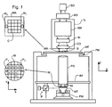
Figure 1 schematically depicts a lithographic apparatus according to one embodiment of the invention. The apparatus comprises: - an illumination system (illuminator) IL configured to condition a radiation beam B (e.g. UV radiation or DUV radiation).
- a support structure (e.g. a mask table) MT constructed to support a patterning device (e.g. a mask) MA and connected to a first positioner PM configured to accurately position the patterning device in accordance with certain parameters;
- a substrate table (e.g. a wafer table) WT constructed to hold a substrate (e.g. a resist-coated wafer) W and connected to a second positioner PW configured to accurately position the substrate in accordance with certain parameters; and
- a projection system (e.g. a refractive projection lens system) PS configured to project a pattern imparted to the radiation beam B by patterning device MA onto a target portion C (e.g. comprising one or more dies) of the substrate W.
- The illumination system may include various types of optical components, such as refractive, reflective, magnetic, electromagnetic, electrostatic or other types of optical components, or any combination thereof, for directing, shaping, or controlling radiation.
- The support structure supports, i.e. bears the weight of, the patterning device. It holds the patterning device in a manner that depends on the orientation of the patterning device, the design of the lithographic apparatus, and other conditions, such as for example whether or not the patterning device is held in a vacuum environment. The support structure can use mechanical, vacuum, electrostatic or other clamping techniques to hold the patterning device. The support structure may be a frame or a table, for example, which may be fixed or movable as required. The support structure may ensure that the patterning device is at a desired position, for example with respect to the projection system. Any use of the terms "reticle" or "mask" herein may be considered synonymous with the more general term "patterning device."
- The term "patterning device" used herein should be broadly interpreted as referring to any device that can be used to impart a radiation beam with a pattern in its cross-section such as to create a pattern in a target portion of the substrate. It should be noted that the pattern imparted to the radiation beam may not exactly correspond to the desired pattern in the target portion of the substrate, for example if the pattern includes phase-shifting features or so called assist features. Generally, the pattern imparted to the radiation beam will correspond to a particular functional layer in a device being created in the target portion, such as an integrated circuit.
- The patterning device may be transmissive or reflective. Examples of patterning devices include masks, programmable mirror arrays, and programmable LCD panels. Masks are well known in lithography, and include mask types such as binary, alternating phase-shift, and attenuated phase-shift, as well as various hybrid mask types. An example of a programmable mirror array employs a matrix arrangement of small mirrors, each of which can be individually tilted so as to reflect an incoming radiation beam in different directions. The tilted mirrors impart a pattern in a radiation beam which is reflected by the mirror matrix.
- The term "projection system" used herein should be broadly interpreted as encompassing any type of projection system, including refractive, reflective, catadioptric, magnetic, electromagnetic and electrostatic optical systems, or any combination thereof, as appropriate for the exposure radiation being used, or for other factors such as the use of an immersion liquid or the use of a vacuum. Any use of the term "projection lens" herein may be considered as synonymous with the more general term "projection system".
- As here depicted, the apparatus is of a transmissive type (e.g. employing a transmissive mask). Alternatively, the apparatus may be of a reflective type (e.g. employing a programmable mirror array of a type as referred to above, or employing a reflective mask).
- The lithographic apparatus may be of a type having two (dual stage) or more substrate tables (and/or two or more mask tables). In such "multiple stage" machines the additional tables may be used in parallel, or preparatory steps may be carried out on one or more tables while one or more other tables are being used for exposure.
- Referring to
Figure 1 , the illuminator IL receives a radiation beam from a radiation source SO. The source and the lithographic apparatus may be separate entities, for example when the source is an excimer laser. In such cases, the source is not considered to form part of the lithographic apparatus and the radiation beam is passed from the source SO to the illuminator IL with the aid of a beam delivery system BD comprising, for example, suitable directing mirrors and/or a beam expander. In other cases the source may be an integral part of the lithographic apparatus, for example when the source is a mercury lamp. The source SO and the illuminator IL, together with the beam delivery system BD if required, may be referred to as a radiation system. - The illuminator IL may comprise an adjuster AD for adjusting the angular intensity distribution of the radiation beam. Generally, at least the outer and/or inner radial extent (commonly referred to as σ-outer and σ-inner, respectively) of the intensity distribution in a pupil plane of the illuminator can be adjusted. In addition, the illuminator IL may comprise various other components, such as an integrator IN and a condenser CO. The illuminator may be used to condition the radiation beam, to have a desired uniformity and intensity distribution in its cross-section.
- The radiation beam B is incident on the patterning device (e.g., mask MA), which is held on the support structure (e.g., mask table MT), and is patterned by the patterning device. Having traversed the mask MA, the radiation beam B passes through the projection system PS, which focuses the beam onto a target portion C of the substrate W. With the aid of the second positioner PW and position sensor IF (e.g. an interferometric device, linear encoder or capacitive sensor), the substrate table WT can be moved accurately, e.g. so as to position different target portions C in the path of the radiation beam B. Similarly, the first positioner PM and another position sensor (which is not explicitly depicted in
Figure 1 ) can be used to accurately position the mask MA with respect to the path of the radiation beam B, e.g. after mechanical retrieval from a mask library, or during a scan. In general, movement of the mask table MT may be realized with the aid of a long-stroke module (coarse positioning) and a short-stroke module (fine positioning), which form part of the first positioner PM. Similarly, movement of the substrate table WT may be realized using a long-stroke module and a short-stroke module, which form part of the second positioner PW. In the case of a stepper (as opposed to a scanner) the mask table MT may be connected to a short-stroke actuator only, or may be fixed. Mask MA and substrate W may be aligned using mask alignment marks M1, M2 and substrate alignment marks P1, P2. Although the substrate alignment marks as illustrated occupy dedicated target portions, they may be located in spaces between target portions (these are known as scribe-lane alignment marks). Similarly, in situations in which more than one die is provided on the mask MA, the mask alignment marks may be located between the dies. - The depicted apparatus could be used in at least one of the following modes:
- 1. In step mode, the mask table MT and the substrate table WT are kept essentially stationary, while an entire pattern imparted to the radiation beam is projected onto a target portion C at one time (i.e. a single static exposure). The substrate table WT is then shifted in the X and/or Y direction so that a different target portion C can be exposed. In step mode, the maximum size of the exposure field limits the size of the target portion C imaged in a single static exposure.
- 2. In scan mode, the mask table MT and the substrate table WT are scanned synchronously while a pattern imparted to the radiation beam is projected onto a target portion C (i.e. a single dynamic exposure). The velocity and direction of the substrate table WT relative to the mask table MT may be determined by the (de-)magnification and image reversal characteristics of the projection system PS. In scan mode, the maximum size of the exposure field limits the width (in the non-scanning direction) of the target portion in a single dynamic exposure, whereas the length of the scanning motion determines the height (in the scanning direction) of the target portion.
- 3. In another mode, the mask table MT is kept essentially stationary holding a programmable patterning device, and the substrate table WT is moved or scanned while a pattern imparted to the radiation beam is projected onto a target portion C. In this mode, generally a pulsed radiation source is employed and the programmable patterning device is updated as required after each movement of the substrate table WT or in between successive radiation pulses during a scan. This mode of operation can be readily applied to maskless lithography that utilizes programmable patterning device, such as a programmable mirror array of a type as referred to above.
- Combinations and/or variations on the above described modes of use or entirely different modes of use may also be employed.
- A further immersion lithography solution with a localized liquid supply system is shown in
Figure 4 . Liquid is supplied by two groove inlets IN on either side of the projection system PL and is removed by a plurality of discrete outlets OUT arranged radially outwardly of the inlets IN. The inlets IN and OUT can be arranged in a plate with a hole in its center and through which the projection beam is projected. Liquid is supplied by one groove inlet IN on one side of the projection system PL and removed by a plurality of discrete outlets OUT on the other side of the projection system PL, causing a flow of a thin film of liquid between the projection system PL and the substrate W. The choice of which combination of inlet IN and outlets OUT to use can depend on the direction of movement of the substrate W (the other combination of inlet IN and outlets OUT being inactive). - Another immersion lithography solution with a localized liquid supply system solution which has been proposed is to provide the liquid supply system with a liquid confinement structure which extends along at least a part of a boundary of the space between the final element of the projection system and the substrate table. The liquid confinement structure is substantially stationary relative to the projection system in the XY plane though there may be some relative movement in the Z direction (in the direction of the optical axis). A seal is formed between the liquid confinement structure and the surface of the substrate. In an embodiment, the seal is a contactless seal such as a gas seal. Such a system with a gas seal is disclosed in
United States patent application no. US 10/705,783US 2004/0207824 ). -
Figure 5 shows a liquid supply system comprising a liquid confinement structure (sometimes referred to as an immersion hood or showerhead) according to an embodiment of the invention. In particular,Figure 5 depicts an arrangement of areservoir 10, which forms a contactless seal to the substrate around the image field of the projection system so that liquid is confined to fill a space between the substrate's primary surface, which faces the projection system PL, and the final element (e.g. an 'abschlussplatte' which seals the projection system, or the final optical element of the projection system) of the projection system PL. Aliquid confinement structure 12 positioned below and surrounding the final element of the projection system PL forms the reservoir. Thus, the liquid supply system provides liquid on only a localized area of the substrate. Theliquid confinement structure 12 forms part of the liquid supply system configured to fill a space between the final element of the projection system and the substrate W (or substrate table WT) with a liquid. Liquid is brought into the space below the projection system and within theliquid confinement structure 12. Theliquid confinement structure 12 extends a little above the final element of the projection system and the liquid level rises above the final element so that a buffer of liquid is provided. Theliquid confinement structure 12 has an inner periphery that at the upper end preferably closely conforms to the shape of the projection system or the final element thereof and may, e.g., be round. At the bottom, the inner periphery closely conforms to the shape of the image field, e.g., rectangular though this need not be the case. The patterned beam passes through this aperture. - The liquid is confined in the reservoir by a
gas seal 16 between the bottom of theliquid confinement structure 12 and the surface of the substrate W. The gas seal is formed by gas, e.g. air, synthetic air, N2 or an inert gas, provided under pressure viainlet 15 to the gap betweenliquid confinement structure 12 and substrate and extracted viaoutlet 14. The overpressure on thegas inlet 15, vacuum level on theoutlet 14 and geometry of the gap are arranged so that there is a high-velocity gas flow inwards that confines the liquid. It will be understood by the person skilled in the art that other types of seal could be used to contain the liquid such as simply an outlet to remove liquid and/or gas. As with any seal, some liquid is likely to escape, for example up theoutlet 14. -
Figures 2, 3 and 4 also depict a liquid reservoir defined by inlet(s) IN, outlet(s) OUT, the substrate W and the final element of projection lens PL. Like the liquid supply system ofFigure 5 , the liquid supply systems illustrated inFigures 2, 3 and 4 , comprising inlet(s) IN and outlet(s) OUT, supply liquid to a space between the final element of the projection system and a localized area of the primary surface of the substrate. - Both of the liquid supply systems of
Figures 2, 3 and 4 as well as other solutions, such as a bath in which the substrate W or whole substrate table WT is submerged, may be used an one or more embodiments of the invention described below. -
Figure 6 illustrates in detail thefinal element 20 of the projection system PL according to an embodiment of the invention. In the embodiment illustrated inFigure 6 , a finaloptical element 20 of the projection system is present which is the last lens element of the projection system PL which shapes and/or directs the patterned beam. - In an embodiment, a material transmissive of radiation at 193 nm is quartz, unless the intensity of the radiation will result in significant compaction effects. The intensity of the radiation of the patterned beam is highest at the final element, which also tends to be the smallest, so that this element is likely to suffer from compaction if made from quartz. Accordingly, in an embodiment, the material for the last element may instead be CaF2 since it does not suffer from compaction at 193 nm. The use of CaF2 is even more applicable for 157 nm radiation as quartz is not transmissive of radiation having this wavelength. However, CaF2 may dissolve or react with immersion liquid 11 used in an immersion lithographic apparatus.
- Several ways of protecting the
final element 20 of the projection system are disclosed inEuropean Patent Application No. 03257400.6 publication number EP 1426821 ). - Another concern with using CaF2 for the final element of the projection system PL is that CaF2 has a very high thermal expansion coefficient (40 times larger than that of fused silica) and may therefore be difficult to mount in the projection system without inducing large thermal stresses and deformations if the mounting materials are different. In the first order, these stresses and deformations change linearly with the difference in expansion coefficients. Thus, mounting a CaF2 optical element may be problematic, particularly for immersion lithographic apparatus, where the positional requirement of the final lens element can be a factor of 2 to 10 times greater than that for non-immersion lithographic apparatus.
- Referring to
Figure 6 , a final element of the projection system according to an embodiment of the invention is depicted. Thebottom surface 25 of the final element (e.g., a lens) 20 of the projection system nearest to the substrate is protected by a fusedsilica layer 40 which is provided on thefinal element 20. This layer may have a thickness in the range of 50µm to 5mm and may be contact bonded or glue bonded to thefinal element 20. In contact bonding, no glue is used - the bonding surfaces are smooth and clean enough to directly bond together. After bonding to the final element, the fusedsilica layer 40 may be ground and polished to the desired thickness, avoiding difficulties inherent in handling a very thin layer of fused silica. Thus, in an embodiment, thelayer 40 andfinal element 20 are bonded together and thefinal element 20 is not merely coated. - Although this form of bonding can provide an exceptionally strong bond where dissimilar materials, such as CaF2 and fused silica, are bonded, temperature changes and thermal gradients may cause the bond to "breathe" - differential thermal expansion or contraction of the two materials causing them to separate until the stress is relieved. Although the bond usually reforms very quickly in the case of thermal separation, if this occurs when the final element is in contact with a liquid, e.g. during polishing or grinding of the
layer 40 or during use of the immersion lithographic apparatus, liquid may be drawn into the gap. - In order to protect the bond between the
final element 20 and thelayer 40, anedge barrier 60 of the same material as thelayer 40 and extending from thelayer 40 away from the substrate (towards the remainder of the projection system PL) completes the barrier around thefinal element 20 such that thefinal element 20 is shielded from the liquid 11. - The
edge barrier 60 is attached around the edge of thelayer 40. As illustrated, theedge barrier 60 is attached adjacent an edge of theplate 40 which extends beyond the edge of thebottom surface 25 of thefinal element 20. Other arrangements are possible, for example by bonding theedge barrier 60 to the edge surface of thelayer 40 rather than to the top surface of theplate 40. In an embodiment, the bond between theedge barrier 60 and thelayer 40 is a fusion bond.PCT Patent Application No. PCT/EP04/013310 WO 2005/054955 ) describes such bonding techniques in detail. In an embodiment, theedge barrier 60 is in the form of a truncated cone. However, theedge barrier 60 may have any shape so long as it creates a cavity which can accommodate thefinal element 20. - The
final element 20 may well have sides that overlap the bottom surface of thefinal element 20 such that, in an embodiment, thelayer 40 overhangs the bottom surface of thefinal element 20 so that theedge barrier 60 can be attached to the top of the surface of thelayer 40. In an embodiment, a gap is left between theedge barrier 60 and thefinal element 20 though this need not be the case. - As is shown in
Figure 6 , thefinal element 20 may be mounted tomounts 80 of the projection system PS body through theedge barrier 60 and through thelayer 40. This is advantageous because temperature and mounting induced stresses and deformations may be reduced significantly because theedge barrier 60 acts as a decoupling between themounts 80 and thefinal element 20. Alternatively, thefinal element 20 may be mounted to themounts 80 directly through thelayer 40. Measurement systems or sensors configured to measure the position of thefinal element 20 may also be attached to thelayer 40 oredge barrier 60. The attachment to the projection system or of the sensors is achievable by conventional means. - Although an embodiment of the invention has been described with the
layer 40 and theedge barrier 60 comprising fused silica, any appropriate material may be used for thelayer 40 and/or theedge barrier 60. In an embodiment, the material used for thelayer 40 and/or theedge barrier 60 is resistant to attack by the immersion liquid, which may be a liquid other than water, and has a coefficient of thermal expansion lower than that of the material of thefinal element 20, which may be a material other than CaF2. In an embodiment, the coefficient of thermal expansion is at least 2 times, 5 times, 10 times or 20 times lower than that of the material of the final element. Thefinal element 20 may be made of any appropriate material. - In
European Patent Application No. 03257072.3 publication number EP 1420300 ), the idea of a twin or dual stage immersion lithography apparatus is disclosed. Such an apparatus is provided with two tables for supporting a substrate. Leveling measurements are carried out with a table at a first position, without immersion liquid, and exposure is carried out with a table at a second position, where immersion liquid is present. Alternatively, the apparatus has only one table. - Although specific reference may be made in this text to the use of lithographic apparatus in the manufacture of ICs, it should be understood that the lithographic apparatus described herein may have other applications, such as the manufacture of integrated optical systems, guidance and detection patterns for magnetic domain memories, flat-panel displays, liquid-crystal displays (LCDs), thin-film magnetic heads, etc. The skilled artisan will appreciate that, in the context of such alternative applications, any use of the terms "wafer" or "die" herein may be considered as synonymous with the more general terms "substrate" or "target portion", respectively. The substrate referred to herein may be processed, before or after exposure, in for example a track (a tool that typically applies a layer of resist to a substrate and develops the exposed resist), a metrology tool and/or an inspection tool. Where applicable, the disclosure herein may be applied to such and other substrate processing tools. Further, the substrate may be processed more than once, for example in order to create a multi-layer IC, so that the term substrate used herein may also refer to a substrate that already contains multiple processed layers.
- Although specific reference may have been made above to the use of embodiments of the invention in the context of optical lithography, it will be appreciated that the invention may be used in other applications, for example imprint lithography, and where the context allows, is not limited to optical lithography. In imprint lithography a topography in a patterning device defines the pattern created on a substrate. The topography of the patterning device may be pressed into a layer of resist supplied to the substrate whereupon the resist is cured by applying electromagnetic radiation, heat, pressure or a combination thereof. The patterning device is moved out of the resist leaving a pattern in it after the resist is cured.
- The terms "radiation" and "beam" used herein encompass all types of electromagnetic radiation, including ultraviolet (UV) radiation (e.g. having a wavelength of or about 365, 248, 193, 157 or 126 nm) and extreme ultra-violet (EUV) radiation (e.g. having a wavelength in the range of 5-20 nm), as well as particle beams, such as ion beams or electron beams.
- The term "lens", where the context allows, may refer to any one or combination of various types of optical components, including refractive, reflective, magnetic, electromagnetic and electrostatic optical components.
- While specific embodiments of the invention have been described above, it will be appreciated that the invention may be practiced otherwise than as described. For example, the invention may take the form of a computer program containing one or more sequences of machine-readable instructions describing a method as disclosed above, or a data storage medium (e.g. semiconductor memory, magnetic or optical disk) having such a computer program stored therein.
- One or more embodiments of the invention may be applied to any immersion lithography apparatus, such as those types mentioned above, and whether the immersion liquid is provided in the form of a bath or only on a localized surface area of the substrate. A liquid supply system is any mechanism that provides a liquid to a space between the projection system and the substrate and/or substrate table. It may comprise any combination of one or more structures, one or more liquid inlets, one or more gas inlets, one or more gas outlets, and/or one or more liquid outlets, the combination providing and confining the liquid to the space. In an embodiment, a surface of the space may be limited to a portion of the substrate and/or substrate table, a surface of the space may completely cover a surface of the substrate and/or substrate table, or the space may envelop the substrate and/or substrate table.
- The descriptions above are intended to be illustrative, not limiting. Thus, it will be apparent to one skilled in the art that modifications may be made to the invention as described without departing from the scope of the claims set out below.
Claims (18)
- A lithographic projection apparatus, comprising:a projection system (PS) configured to project a patterned beam of radiation onto a substrate (W), the projection system comprising a final element (20) having a layer (40) on a surface (25) nearest the substrate; anda liquid supply system (IH) configured to at least partly fill a space between the final element of the projection system and the substrate with a liquid;characterized in that the final element is attached to the apparatus through the layer.
- The apparatus of claim 1, further comprising an edge barrier (60), of the same material as the layer, extending from the layer away from the substrate to shield the final element from the liquid.
- The apparatus of claim 2, wherein the layer is a plate and the final element is attached to the apparatus through the layer and through the edge barrier.
- The apparatus of any one of claim 1-3, wherein the layer is contact bonded to the final element.
- The apparatus of any one of claims 1-3, wherein the layer has a coefficient of thermal expansion lower than the coefficient of thermal expansion of the final element, preferably 10 times lower than the coefficient of thermal expansion of the final element.
- The lithographic projection apparatus of claim 1, wherein: said layer is bonded to said surface nearest the substrate and said projection system further comprises an edge barrier, of the same material as the layer, extending from the layer away from the substrate to shield the final element from a liquid.
- The apparatus of claim 6, wherein the edge barrier is fusion bonded to the layer.
- The apparatus of claim 6 or 7, wherein the edge barrier does not contact the final element.
- The apparatus of claim 6, 7 or 8, wherein the final element is mounted to the apparatus by connection through the edge barrier.
- The apparatus of any one of the preceding claims, wherein the layer is a plate.
- The apparatus of any one of the preceding claims, wherein the layer and barrier member comprise fused silica.
- The apparatus of any one of claims 1-5, wherein the final element comprises CaF2.
- The apparatus of any one of the preceding claims, wherein the edge barrier is in the shape of a truncated cone.
- The apparatus of any one of the preceding claims, wherein the layer is contact bonded to the surface.
- A device manufacturing method, comprising:using a lithographic projection apparatus to project a patterned beam of radiation onto a substrate (W) through a liquid provided in a space between a final element (20) of a projection system and the substrate, wherein the final element has on a surface (25) nearest the substrate a layer (40) through which the final element is attached to said apparatus.
- A device manufacturing method according to claim 15, wherein an edge barrier of the same material as the layer extends from the layer away from the substrate to shield the final element from the liquid.
- The apparatus of any one of claims 1-14 or the method of claim 15 or 16, wherein the layer is substantially insoluble in the liquid.
- The apparatus or method of any one of the preceding claims, wherein the layer has a coefficient of thermal expansion lower than the coefficient of thermal expansion of the final element.
Applications Claiming Priority (1)
| Application Number | Priority Date | Filing Date | Title |
|---|---|---|---|
| US11/022,939 US7405805B2 (en) | 2004-12-28 | 2004-12-28 | Lithographic apparatus and device manufacturing method |
Publications (2)
| Publication Number | Publication Date |
|---|---|
| EP1677153A1 EP1677153A1 (en) | 2006-07-05 |
| EP1677153B1 true EP1677153B1 (en) | 2009-06-03 |
Family
ID=35735374
Family Applications (1)
| Application Number | Title | Priority Date | Filing Date |
|---|---|---|---|
| EP20050257739 Expired - Fee Related EP1677153B1 (en) | 2004-12-28 | 2005-12-15 | Lithographic apparatus and device manufacturing method |
Country Status (8)
| Country | Link |
|---|---|
| US (3) | US7405805B2 (en) |
| EP (1) | EP1677153B1 (en) |
| JP (1) | JP4383408B2 (en) |
| KR (1) | KR100742766B1 (en) |
| CN (1) | CN100510968C (en) |
| DE (1) | DE602005014731D1 (en) |
| SG (2) | SG123750A1 (en) |
| TW (1) | TWI329790B (en) |
Families Citing this family (11)
| Publication number | Priority date | Publication date | Assignee | Title |
|---|---|---|---|---|
| KR101204157B1 (en) | 2004-01-20 | 2012-11-22 | 칼 짜이스 에스엠테 게엠베하 | Microlithographic projection exposure apparatus and measuring device for a projection lens |
| US7405805B2 (en) * | 2004-12-28 | 2008-07-29 | Asml Netherlands B.V. | Lithographic apparatus and device manufacturing method |
| US7450217B2 (en) | 2005-01-12 | 2008-11-11 | Asml Netherlands B.V. | Exposure apparatus, coatings for exposure apparatus, lithographic apparatus, device manufacturing method, and device manufactured thereby |
| DE102005024163A1 (en) * | 2005-05-23 | 2006-11-30 | Carl Zeiss Smt Ag | Optical system e.g. projection objective, for microlithography projection exposure system, has module insertable and removable as unit into system, and concave curved optical surface for capping cavity during operation of exposure system |
| GB2431670A (en) * | 2005-10-25 | 2007-05-02 | Zeiss Carl Smt Ag | Protective coating with windows for protection of optical element that is soluble in immersion liquid. |
| JP4514225B2 (en) * | 2005-11-16 | 2010-07-28 | キヤノン株式会社 | Exposure apparatus and device manufacturing method |
| DE102006021797A1 (en) | 2006-05-09 | 2007-11-15 | Carl Zeiss Smt Ag | Optical imaging device with thermal damping |
| NL2003363A (en) * | 2008-09-10 | 2010-03-15 | Asml Netherlands Bv | Lithographic apparatus, method of manufacturing an article for a lithographic apparatus and device manufacturing method. |
| NL2003392A (en) | 2008-09-17 | 2010-03-18 | Asml Netherlands Bv | Lithographic apparatus and a method of operating the apparatus. |
| NL2004497A (en) * | 2009-05-01 | 2010-11-02 | Asml Netherlands Bv | Lithographic apparatus and a method of operating the apparatus. |
| CN106474858A (en) * | 2015-08-26 | 2017-03-08 | 盐城市瓯华化学工业有限公司 | Gas-liquid cycle separator for chemical material production |
Family Cites Families (117)
| Publication number | Priority date | Publication date | Assignee | Title |
|---|---|---|---|---|
| DE242880C (en) | ||||
| DE224448C (en) | ||||
| DE206607C (en) | ||||
| DE221563C (en) | ||||
| GB1242527A (en) | 1967-10-20 | 1971-08-11 | Kodak Ltd | Optical instruments |
| US3573975A (en) | 1968-07-10 | 1971-04-06 | Ibm | Photochemical fabrication process |
| EP0023231B1 (en) | 1979-07-27 | 1982-08-11 | Tabarelli, Werner, Dr. | Optical lithographic method and apparatus for copying a pattern onto a semiconductor wafer |
| FR2474708B1 (en) | 1980-01-24 | 1987-02-20 | Dme | HIGH-RESOLUTION MICROPHOTOLITHOGRAPHY PROCESS |
| JPS5754317A (en) | 1980-09-19 | 1982-03-31 | Hitachi Ltd | Method and device for forming pattern |
| US4509852A (en) | 1980-10-06 | 1985-04-09 | Werner Tabarelli | Apparatus for the photolithographic manufacture of integrated circuit elements |
| US4346164A (en) | 1980-10-06 | 1982-08-24 | Werner Tabarelli | Photolithographic method for the manufacture of integrated circuits |
| US4390273A (en) | 1981-02-17 | 1983-06-28 | Censor Patent-Und Versuchsanstalt | Projection mask as well as a method and apparatus for the embedding thereof and projection printing system |
| JPS57153433A (en) | 1981-03-18 | 1982-09-22 | Hitachi Ltd | Manufacturing device for semiconductor |
| JPS58202448A (en) | 1982-05-21 | 1983-11-25 | Hitachi Ltd | Exposing device |
| DD206607A1 (en) | 1982-06-16 | 1984-02-01 | Mikroelektronik Zt Forsch Tech | METHOD AND DEVICE FOR ELIMINATING INTERFERENCE EFFECTS |
| DD242880A1 (en) | 1983-01-31 | 1987-02-11 | Kuch Karl Heinz | DEVICE FOR PHOTOLITHOGRAPHIC STRUCTURAL TRANSMISSION |
| DD221563A1 (en) | 1983-09-14 | 1985-04-24 | Mikroelektronik Zt Forsch Tech | IMMERSIONS OBJECTIVE FOR THE STEP-BY-STEP PROJECTION IMAGING OF A MASK STRUCTURE |
| DD224448A1 (en) | 1984-03-01 | 1985-07-03 | Zeiss Jena Veb Carl | DEVICE FOR PHOTOLITHOGRAPHIC STRUCTURAL TRANSMISSION |
| JPS6265326A (en) | 1985-09-18 | 1987-03-24 | Hitachi Ltd | Exposure device |
| JPS62121417A (en) | 1985-11-22 | 1987-06-02 | Hitachi Ltd | Liquid-immersion objective lens device |
| JPS63157419A (en) | 1986-12-22 | 1988-06-30 | Toshiba Corp | Fine pattern transfer apparatus |
| US5040020A (en) | 1988-03-31 | 1991-08-13 | Cornell Research Foundation, Inc. | Self-aligned, high resolution resonant dielectric lithography |
| JPH03209479A (en) | 1989-09-06 | 1991-09-12 | Sanee Giken Kk | Exposure method |
| US5121256A (en) | 1991-03-14 | 1992-06-09 | The Board Of Trustees Of The Leland Stanford Junior University | Lithography system employing a solid immersion lens |
| JPH04305917A (en) | 1991-04-02 | 1992-10-28 | Nikon Corp | Adhesion type exposure device |
| JPH04305915A (en) | 1991-04-02 | 1992-10-28 | Nikon Corp | Adhesion type exposure device |
| JPH06124873A (en) | 1992-10-09 | 1994-05-06 | Canon Inc | Liquid-soaking type projection exposure apparatus |
| JP2753930B2 (en) | 1992-11-27 | 1998-05-20 | キヤノン株式会社 | Immersion type projection exposure equipment |
| JP2520833B2 (en) | 1992-12-21 | 1996-07-31 | 東京エレクトロン株式会社 | Immersion type liquid treatment device |
| JPH07220990A (en) | 1994-01-28 | 1995-08-18 | Hitachi Ltd | Pattern forming method and exposure apparatus therefor |
| US6104687A (en) | 1996-08-26 | 2000-08-15 | Digital Papyrus Corporation | Method and apparatus for coupling an optical lens to a disk through a coupling medium having a relatively high index of refraction |
| US5825043A (en) | 1996-10-07 | 1998-10-20 | Nikon Precision Inc. | Focusing and tilting adjustment system for lithography aligner, manufacturing apparatus or inspection apparatus |
| JP3612920B2 (en) | 1997-02-14 | 2005-01-26 | ソニー株式会社 | Exposure apparatus for producing an optical recording medium master |
| JPH10255319A (en) | 1997-03-12 | 1998-09-25 | Hitachi Maxell Ltd | Master disk exposure device and method therefor |
| JP3747566B2 (en) | 1997-04-23 | 2006-02-22 | 株式会社ニコン | Immersion exposure equipment |
| JP3817836B2 (en) | 1997-06-10 | 2006-09-06 | 株式会社ニコン | EXPOSURE APPARATUS, ITS MANUFACTURING METHOD, EXPOSURE METHOD, AND DEVICE MANUFACTURING METHOD |
| US5900354A (en) | 1997-07-03 | 1999-05-04 | Batchelder; John Samuel | Method for optical inspection and lithography |
| JPH11176727A (en) | 1997-12-11 | 1999-07-02 | Nikon Corp | Projection aligner |
| WO1999031717A1 (en) | 1997-12-12 | 1999-06-24 | Nikon Corporation | Projection exposure method and projection aligner |
| WO1999049504A1 (en) | 1998-03-26 | 1999-09-30 | Nikon Corporation | Projection exposure method and system |
| JP2000058436A (en) | 1998-08-11 | 2000-02-25 | Nikon Corp | Projection aligner and exposure method |
| TWI242111B (en) | 1999-04-19 | 2005-10-21 | Asml Netherlands Bv | Gas bearings for use in vacuum chambers and their application in lithographic projection apparatus |
| JP4504479B2 (en) | 1999-09-21 | 2010-07-14 | オリンパス株式会社 | Immersion objective lens for microscope |
| TW591653B (en) | 2000-08-08 | 2004-06-11 | Koninkl Philips Electronics Nv | Method of manufacturing an optically scannable information carrier |
| JP2002072090A (en) * | 2000-08-31 | 2002-03-12 | Olympus Optical Co Ltd | Wide-angle zoom lens |
| US20020163629A1 (en) | 2001-05-07 | 2002-11-07 | Michael Switkes | Methods and apparatus employing an index matching medium |
| US6600547B2 (en) | 2001-09-24 | 2003-07-29 | Nikon Corporation | Sliding seal |
| EP1446703A2 (en) | 2001-11-07 | 2004-08-18 | Applied Materials, Inc. | Optical spot grid array printer |
| US7092069B2 (en) | 2002-03-08 | 2006-08-15 | Carl Zeiss Smt Ag | Projection exposure method and projection exposure system |
| DE10229818A1 (en) | 2002-06-28 | 2004-01-15 | Carl Zeiss Smt Ag | Focus detection method and imaging system with focus detection system |
| US6788477B2 (en) | 2002-10-22 | 2004-09-07 | Taiwan Semiconductor Manufacturing Co., Ltd. | Apparatus for method for immersion lithography |
| CN101382738B (en) | 2002-11-12 | 2011-01-12 | Asml荷兰有限公司 | Lithographic projection apparatus |
| SG135052A1 (en) | 2002-11-12 | 2007-09-28 | Asml Netherlands Bv | Lithographic apparatus and device manufacturing method |
| SG121822A1 (en) | 2002-11-12 | 2006-05-26 | Asml Netherlands Bv | Lithographic apparatus and device manufacturing method |
| KR100588124B1 (en) | 2002-11-12 | 2006-06-09 | 에이에스엠엘 네델란즈 비.브이. | Lithographic Apparatus and Device Manufacturing Method |
| DE60335595D1 (en) | 2002-11-12 | 2011-02-17 | Asml Netherlands Bv | Immersion lithographic apparatus and method of making a device |
| SG131766A1 (en) | 2002-11-18 | 2007-05-28 | Asml Netherlands Bv | Lithographic apparatus and device manufacturing method |
| TWI243288B (en) * | 2002-11-26 | 2005-11-11 | Asml Netherlands Bv | Method of fabricating an optical element, lithographic apparatus and semiconductor device manufacturing method |
| AU2003302831A1 (en) | 2002-12-10 | 2004-06-30 | Nikon Corporation | Exposure method, exposure apparatus and method for manufacturing device |
| SG152063A1 (en) | 2002-12-10 | 2009-05-29 | Nikon Corp | Exposure apparatus and method for producing device |
| JP4352874B2 (en) | 2002-12-10 | 2009-10-28 | 株式会社ニコン | Exposure apparatus and device manufacturing method |
| WO2004053957A1 (en) | 2002-12-10 | 2004-06-24 | Nikon Corporation | Surface position detection apparatus, exposure method, and device porducing method |
| WO2004053952A1 (en) | 2002-12-10 | 2004-06-24 | Nikon Corporation | Exposure apparatus and method for manufacturing device |
| DE10257766A1 (en) | 2002-12-10 | 2004-07-15 | Carl Zeiss Smt Ag | Method for setting a desired optical property of a projection lens and microlithographic projection exposure system |
| TW200421444A (en) | 2002-12-10 | 2004-10-16 | Nippon Kogaku Kk | Optical device and projecting exposure apparatus using such optical device |
| KR101101737B1 (en) | 2002-12-10 | 2012-01-05 | 가부시키가이샤 니콘 | Exposure apparatus, exposure method and method for manufacturing device |
| AU2003289237A1 (en) | 2002-12-10 | 2004-06-30 | Nikon Corporation | Exposure apparatus and method for manufacturing device |
| US7242455B2 (en) | 2002-12-10 | 2007-07-10 | Nikon Corporation | Exposure apparatus and method for producing device |
| KR20120127755A (en) | 2002-12-10 | 2012-11-23 | 가부시키가이샤 니콘 | Exposure apparatus and method for manufacturing device |
| KR20130010039A (en) | 2002-12-10 | 2013-01-24 | 가부시키가이샤 니콘 | Exposure system and device producing method |
| JP4232449B2 (en) | 2002-12-10 | 2009-03-04 | 株式会社ニコン | Exposure method, exposure apparatus, and device manufacturing method |
| CN100370533C (en) | 2002-12-13 | 2008-02-20 | 皇家飞利浦电子股份有限公司 | Liquid removal in a method and device for irradiating spots on a layer |
| EP1579435B1 (en) | 2002-12-19 | 2007-06-27 | Koninklijke Philips Electronics N.V. | Method and device for irradiating spots on a layer |
| EP1732075A3 (en) | 2002-12-19 | 2007-02-21 | Koninklijke Philips Electronics N.V. | Method and device for irradiating spots on a layer |
| WO2004093159A2 (en) | 2003-04-09 | 2004-10-28 | Nikon Corporation | Immersion lithography fluid control system |
| EP2921905B1 (en) | 2003-04-10 | 2017-12-27 | Nikon Corporation | Run-off path to collect liquid for an immersion lithography apparatus |
| KR101323993B1 (en) | 2003-04-10 | 2013-10-30 | 가부시키가이샤 니콘 | Environmental system including a transport region for an immersion lithography apparatus |
| WO2004090633A2 (en) | 2003-04-10 | 2004-10-21 | Nikon Corporation | An electro-osmotic element for an immersion lithography apparatus |
| KR20180089562A (en) | 2003-04-10 | 2018-08-08 | 가부시키가이샤 니콘 | Environmental system including vaccum scavange for an immersion lithography apparatus |
| WO2004092830A2 (en) | 2003-04-11 | 2004-10-28 | Nikon Corporation | Liquid jet and recovery system for immersion lithography |
| ATE449982T1 (en) | 2003-04-11 | 2009-12-15 | Nikon Corp | CLEANING PROCESS FOR OPTICS IN IMMERSION LITHOGRAPHY |
| SG194264A1 (en) | 2003-04-11 | 2013-11-29 | Nikon Corp | Apparatus having an immersion fluid system configured to maintain immersion fluid in a gap adjacent an optical assembly |
| WO2004095135A2 (en) | 2003-04-17 | 2004-11-04 | Nikon Corporation | Optical arrangement of autofocus elements for use with immersion lithography |
| TWI295414B (en) | 2003-05-13 | 2008-04-01 | Asml Netherlands Bv | Lithographic apparatus and device manufacturing method |
| US7274472B2 (en) | 2003-05-28 | 2007-09-25 | Timbre Technologies, Inc. | Resolution enhanced optical metrology |
| DE10324477A1 (en) * | 2003-05-30 | 2004-12-30 | Carl Zeiss Smt Ag | Microlithographic projection exposure system |
| EP1486827B1 (en) | 2003-06-11 | 2011-11-02 | ASML Netherlands B.V. | Lithographic apparatus and device manufacturing method |
| JP4343597B2 (en) | 2003-06-25 | 2009-10-14 | キヤノン株式会社 | Exposure apparatus and device manufacturing method |
| JP2005019616A (en) | 2003-06-25 | 2005-01-20 | Canon Inc | Immersion type exposure apparatus |
| EP1498778A1 (en) | 2003-06-27 | 2005-01-19 | ASML Netherlands B.V. | Lithographic apparatus and device manufacturing method |
| JP3862678B2 (en) | 2003-06-27 | 2006-12-27 | キヤノン株式会社 | Exposure apparatus and device manufacturing method |
| EP1652003B1 (en) | 2003-07-08 | 2015-01-07 | Nikon Corporation | Wafer table for immersion lithography |
| US7738074B2 (en) | 2003-07-16 | 2010-06-15 | Asml Netherlands B.V. | Lithographic apparatus and device manufacturing method |
| US8149381B2 (en) * | 2003-08-26 | 2012-04-03 | Nikon Corporation | Optical element and exposure apparatus |
| US6954256B2 (en) * | 2003-08-29 | 2005-10-11 | Asml Netherlands B.V. | Gradient immersion lithography |
| US7070915B2 (en) | 2003-08-29 | 2006-07-04 | Tokyo Electron Limited | Method and system for drying a substrate |
| KR101238114B1 (en) | 2003-09-03 | 2013-02-27 | 가부시키가이샤 니콘 | Apparatus and method for providing fluid for immersion lithography |
| JP4378136B2 (en) | 2003-09-04 | 2009-12-02 | キヤノン株式会社 | Exposure apparatus and device manufacturing method |
| JP3870182B2 (en) | 2003-09-09 | 2007-01-17 | キヤノン株式会社 | Exposure apparatus and device manufacturing method |
| JP2005159322A (en) | 2003-10-31 | 2005-06-16 | Nikon Corp | Surface plate, stage apparatus, exposure device and exposing method |
| US8854602B2 (en) * | 2003-11-24 | 2014-10-07 | Asml Netherlands B.V. | Holding device for an optical element in an objective |
| US7545481B2 (en) * | 2003-11-24 | 2009-06-09 | Asml Netherlands B.V. | Lithographic apparatus and device manufacturing method |
| JP2005175016A (en) | 2003-12-08 | 2005-06-30 | Canon Inc | Substrate holding device, exposure device using the same, and method of manufacturing device |
| JP2005175034A (en) | 2003-12-09 | 2005-06-30 | Canon Inc | Aligner |
| JP2005189850A (en) * | 2003-12-15 | 2005-07-14 | Carl Zeiss Smt Ag | Refractive projection objective lens for immersion lithography |
| JP5102492B2 (en) | 2003-12-19 | 2012-12-19 | カール・ツァイス・エスエムティー・ゲーエムベーハー | Objective lens for microlithography projection with crystal elements |
| US7460206B2 (en) * | 2003-12-19 | 2008-12-02 | Carl Zeiss Smt Ag | Projection objective for immersion lithography |
| US7589818B2 (en) | 2003-12-23 | 2009-09-15 | Asml Netherlands B.V. | Lithographic apparatus, alignment apparatus, device manufacturing method, and a method of converting an apparatus |
| JP2005191381A (en) | 2003-12-26 | 2005-07-14 | Canon Inc | Exposure method and system thereof |
| JP2005191393A (en) | 2003-12-26 | 2005-07-14 | Canon Inc | Exposing method and equipment |
| JP4429023B2 (en) | 2004-01-07 | 2010-03-10 | キヤノン株式会社 | Exposure apparatus and device manufacturing method |
| JP4018647B2 (en) | 2004-02-09 | 2007-12-05 | キヤノン株式会社 | Projection exposure apparatus and device manufacturing method |
| JP4510494B2 (en) | 2004-03-29 | 2010-07-21 | キヤノン株式会社 | Exposure equipment |
| JP2005286068A (en) | 2004-03-29 | 2005-10-13 | Canon Inc | Exposure device and method therefor |
| US7180572B2 (en) * | 2004-06-23 | 2007-02-20 | Taiwan Semiconductor Manufacturing Company, Ltd. | Immersion optical projection system |
| JP2006165285A (en) | 2004-12-08 | 2006-06-22 | Nikon Corp | Optical element and aligner |
| US7405805B2 (en) * | 2004-12-28 | 2008-07-29 | Asml Netherlands B.V. | Lithographic apparatus and device manufacturing method |
-
2004
- 2004-12-28 US US11/022,939 patent/US7405805B2/en not_active Expired - Fee Related
-
2005
- 2005-12-15 EP EP20050257739 patent/EP1677153B1/en not_active Expired - Fee Related
- 2005-12-15 DE DE200560014731 patent/DE602005014731D1/en active Active
- 2005-12-16 TW TW94144968A patent/TWI329790B/en not_active IP Right Cessation
- 2005-12-22 SG SG200508320A patent/SG123750A1/en unknown
- 2005-12-22 SG SG200804540-3A patent/SG144153A1/en unknown
- 2005-12-23 CN CN 200510003549 patent/CN100510968C/en not_active Expired - Fee Related
- 2005-12-27 JP JP2005375770A patent/JP4383408B2/en not_active Expired - Fee Related
- 2005-12-28 KR KR1020050132238A patent/KR100742766B1/en not_active IP Right Cessation
-
2008
- 2008-06-20 US US12/213,543 patent/US8013978B2/en not_active Expired - Fee Related
-
2011
- 2011-07-22 US US13/189,288 patent/US8913225B2/en not_active Expired - Fee Related
Also Published As
| Publication number | Publication date |
|---|---|
| SG123750A1 (en) | 2006-07-26 |
| TW200629002A (en) | 2006-08-16 |
| SG144153A1 (en) | 2008-07-29 |
| US7405805B2 (en) | 2008-07-29 |
| US8913225B2 (en) | 2014-12-16 |
| US20110279796A1 (en) | 2011-11-17 |
| US8013978B2 (en) | 2011-09-06 |
| JP4383408B2 (en) | 2009-12-16 |
| CN100510968C (en) | 2009-07-08 |
| JP2006191066A (en) | 2006-07-20 |
| DE602005014731D1 (en) | 2009-07-16 |
| TWI329790B (en) | 2010-09-01 |
| US20080259296A1 (en) | 2008-10-23 |
| CN1797208A (en) | 2006-07-05 |
| US20060139589A1 (en) | 2006-06-29 |
| EP1677153A1 (en) | 2006-07-05 |
| KR20060076752A (en) | 2006-07-04 |
| KR100742766B1 (en) | 2007-07-25 |
Similar Documents
| Publication | Publication Date | Title |
|---|---|---|
| EP1677153B1 (en) | Lithographic apparatus and device manufacturing method | |
| EP1510871B1 (en) | Lithographic apparatus and device manufacturing method | |
| US8115905B2 (en) | Lithographic apparatus and device manufacturing method | |
| US20190258174A1 (en) | Lithographic apparatus and device manufacturing method involving a liquid confinement structure | |
| EP1720074B1 (en) | Lithographic apparatus and device manufacturing method | |
| US7251013B2 (en) | Lithographic apparatus and device manufacturing method | |
| EP1645911A1 (en) | Lithographic apparatus and device manufacturing method | |
| US20170038695A1 (en) | Lithographic apparatus and device manufacturing method | |
| EP2267536B1 (en) | Lithographic apparatus | |
| EP2261740B1 (en) | Lithographic apparatus | |
| EP1528432B1 (en) | Lithographic apparatus and device manufacturing method | |
| US8054445B2 (en) | Lithographic apparatus and device manufacturing method |
Legal Events
| Date | Code | Title | Description |
|---|---|---|---|
| PUAI | Public reference made under article 153(3) epc to a published international application that has entered the european phase |
Free format text: ORIGINAL CODE: 0009012 |
|
| AK | Designated contracting states |
Kind code of ref document: A1 Designated state(s): AT BE BG CH CY CZ DE DK EE ES FI FR GB GR HU IE IS IT LI LT LU LV MC NL PL PT RO SE SI SK TR |
|
| AX | Request for extension of the european patent |
Extension state: AL BA HR MK YU |
|
| 17P | Request for examination filed |
Effective date: 20060728 |
|
| 17Q | First examination report despatched |
Effective date: 20060824 |
|
| AKX | Designation fees paid |
Designated state(s): DE FR GB IT NL |
|
| GRAP | Despatch of communication of intention to grant a patent |
Free format text: ORIGINAL CODE: EPIDOSNIGR1 |
|
| GRAS | Grant fee paid |
Free format text: ORIGINAL CODE: EPIDOSNIGR3 |
|
| GRAA | (expected) grant |
Free format text: ORIGINAL CODE: 0009210 |
|
| AK | Designated contracting states |
Kind code of ref document: B1 Designated state(s): DE FR GB IT NL |
|
| REG | Reference to a national code |
Ref country code: GB Ref legal event code: FG4D |
|
| REF | Corresponds to: |
Ref document number: 602005014731 Country of ref document: DE Date of ref document: 20090716 Kind code of ref document: P |
|
| NLV1 | Nl: lapsed or annulled due to failure to fulfill the requirements of art. 29p and 29m of the patents act | ||
| PG25 | Lapsed in a contracting state [announced via postgrant information from national office to epo] |
Ref country code: NL Free format text: LAPSE BECAUSE OF FAILURE TO SUBMIT A TRANSLATION OF THE DESCRIPTION OR TO PAY THE FEE WITHIN THE PRESCRIBED TIME-LIMIT Effective date: 20090603 |
|
| PLBE | No opposition filed within time limit |
Free format text: ORIGINAL CODE: 0009261 |
|
| STAA | Information on the status of an ep patent application or granted ep patent |
Free format text: STATUS: NO OPPOSITION FILED WITHIN TIME LIMIT |
|
| 26N | No opposition filed |
Effective date: 20100304 |
|
| GBPC | Gb: european patent ceased through non-payment of renewal fee |
Effective date: 20091215 |
|
| PG25 | Lapsed in a contracting state [announced via postgrant information from national office to epo] |
Ref country code: GB Free format text: LAPSE BECAUSE OF NON-PAYMENT OF DUE FEES Effective date: 20091215 |
|
| PG25 | Lapsed in a contracting state [announced via postgrant information from national office to epo] |
Ref country code: IT Free format text: LAPSE BECAUSE OF FAILURE TO SUBMIT A TRANSLATION OF THE DESCRIPTION OR TO PAY THE FEE WITHIN THE PRESCRIBED TIME-LIMIT Effective date: 20090603 |
|
| REG | Reference to a national code |
Ref country code: FR Ref legal event code: PLFP Year of fee payment: 11 |
|
| PGFP | Annual fee paid to national office [announced via postgrant information from national office to epo] |
Ref country code: DE Payment date: 20151211 Year of fee payment: 11 |
|
| PGFP | Annual fee paid to national office [announced via postgrant information from national office to epo] |
Ref country code: FR Payment date: 20151221 Year of fee payment: 11 |
|
| REG | Reference to a national code |
Ref country code: DE Ref legal event code: R119 Ref document number: 602005014731 Country of ref document: DE |
|
| REG | Reference to a national code |
Ref country code: FR Ref legal event code: ST Effective date: 20170831 |
|
| PG25 | Lapsed in a contracting state [announced via postgrant information from national office to epo] |
Ref country code: FR Free format text: LAPSE BECAUSE OF NON-PAYMENT OF DUE FEES Effective date: 20170102 |
|
| PG25 | Lapsed in a contracting state [announced via postgrant information from national office to epo] |
Ref country code: DE Free format text: LAPSE BECAUSE OF NON-PAYMENT OF DUE FEES Effective date: 20170701 |