EP1677522A1 - Photo detecting apparatus - Google Patents
Photo detecting apparatus Download PDFInfo
- Publication number
- EP1677522A1 EP1677522A1 EP04788187A EP04788187A EP1677522A1 EP 1677522 A1 EP1677522 A1 EP 1677522A1 EP 04788187 A EP04788187 A EP 04788187A EP 04788187 A EP04788187 A EP 04788187A EP 1677522 A1 EP1677522 A1 EP 1677522A1
- Authority
- EP
- European Patent Office
- Prior art keywords
- section
- voltage value
- pixel
- terminal
- outputted
- Prior art date
- Legal status (The legal status is an assumption and is not a legal conclusion. Google has not performed a legal analysis and makes no representation as to the accuracy of the status listed.)
- Granted
Links
- 230000003071 parasitic effect Effects 0.000 claims abstract description 54
- 238000007599 discharging Methods 0.000 claims abstract description 26
- 239000004065 semiconductor Substances 0.000 claims description 19
- 230000005540 biological transmission Effects 0.000 claims description 18
- 238000000034 method Methods 0.000 claims description 16
- 238000005513 bias potential Methods 0.000 claims description 10
- 230000035945 sensitivity Effects 0.000 abstract description 25
- 229920006395 saturated elastomer Polymers 0.000 description 35
- 238000010586 diagram Methods 0.000 description 31
- 238000010276 construction Methods 0.000 description 28
- 238000006243 chemical reaction Methods 0.000 description 4
- 239000000758 substrate Substances 0.000 description 3
- 230000003321 amplification Effects 0.000 description 2
- 238000003199 nucleic acid amplification method Methods 0.000 description 2
- 230000003247 decreasing effect Effects 0.000 description 1
- 230000000694 effects Effects 0.000 description 1
- 238000005516 engineering process Methods 0.000 description 1
- 238000012840 feeding operation Methods 0.000 description 1
- 230000010354 integration Effects 0.000 description 1
Images


Classifications
-
- H—ELECTRICITY
- H01—ELECTRIC ELEMENTS
- H01L—SEMICONDUCTOR DEVICES NOT COVERED BY CLASS H10
- H01L33/00—Semiconductor devices with at least one potential-jump barrier or surface barrier specially adapted for light emission; Processes or apparatus specially adapted for the manufacture or treatment thereof or of parts thereof; Details thereof
- H01L33/02—Semiconductor devices with at least one potential-jump barrier or surface barrier specially adapted for light emission; Processes or apparatus specially adapted for the manufacture or treatment thereof or of parts thereof; Details thereof characterised by the semiconductor bodies
-
- H—ELECTRICITY
- H01—ELECTRIC ELEMENTS
- H01L—SEMICONDUCTOR DEVICES NOT COVERED BY CLASS H10
- H01L27/00—Devices consisting of a plurality of semiconductor or other solid-state components formed in or on a common substrate
- H01L27/14—Devices consisting of a plurality of semiconductor or other solid-state components formed in or on a common substrate including semiconductor components sensitive to infrared radiation, light, electromagnetic radiation of shorter wavelength or corpuscular radiation and specially adapted either for the conversion of the energy of such radiation into electrical energy or for the control of electrical energy by such radiation
- H01L27/144—Devices controlled by radiation
- H01L27/146—Imager structures
- H01L27/14601—Structural or functional details thereof
- H01L27/14609—Pixel-elements with integrated switching, control, storage or amplification elements
-
- H—ELECTRICITY
- H04—ELECTRIC COMMUNICATION TECHNIQUE
- H04N—PICTORIAL COMMUNICATION, e.g. TELEVISION
- H04N23/00—Cameras or camera modules comprising electronic image sensors; Control thereof
- H04N23/70—Circuitry for compensating brightness variation in the scene
-
- H—ELECTRICITY
- H04—ELECTRIC COMMUNICATION TECHNIQUE
- H04N—PICTORIAL COMMUNICATION, e.g. TELEVISION
- H04N25/00—Circuitry of solid-state image sensors [SSIS]; Control thereof
- H04N25/50—Control of the SSIS exposure
- H04N25/57—Control of the dynamic range
- H04N25/571—Control of the dynamic range involving a non-linear response
- H04N25/573—Control of the dynamic range involving a non-linear response the logarithmic type
-
- H—ELECTRICITY
- H04—ELECTRIC COMMUNICATION TECHNIQUE
- H04N—PICTORIAL COMMUNICATION, e.g. TELEVISION
- H04N25/00—Circuitry of solid-state image sensors [SSIS]; Control thereof
- H04N25/50—Control of the SSIS exposure
- H04N25/57—Control of the dynamic range
- H04N25/571—Control of the dynamic range involving a non-linear response
- H04N25/575—Control of the dynamic range involving a non-linear response with a response composed of multiple slopes
Definitions
- the present invention relates to a photo-detecting apparatus having a pixel section of an active-pixel type including a photodiode.
- a photo-detecting apparatus using CMOS technology is known; especially, the one of an active-pixel type system is known (see Patent Reference 1).
- the photo-detecting apparatus of the active-pixel system has a picture element or pixel section of an active-pixel type including a photodiode for generating the amount of an electric charge corresponding to intensity of incident light, and converts the electric charge generated at the photodiode into a voltage, namely carries out charge-to-voltage conversion by way of a source follower circuit constituting transistors, which enables photodetection with high sensitivity and low noise.
- C f the capacitance value of the parasitic capacitance section that stores the electric charge generated at the photodiode
- Q is the amount of the electric charge.
- an upper limit of the output voltage value V is a level of several voltages due to the range of an applicable voltage of a power source and circuit-based restrictions.
- an upper limit in the amount Q of the electric charge that can be accumulated in the parasitic capacitance section is also an upper limit in the amount Q of the electric charge that can be accumulated in the parasitic capacitance section.
- the inventors et al. find out the following problems. That is, though the conventional photo-detecting apparatus can perform photodetection with high sensitivity, there is a problem that the dynamic range of the photodetection is narrowed due to restrictions of the amount of saturated electric charge.
- the present invention is made to solve the aforementioned problem, and it is an object to provide a photo-detecting apparatus having a structure which enables photodetection with high sensitivity and wide dynamic range.
- a photo-detecting apparatus is characterized by comprising: (1) a pixel section including a photodiode for generating an electric charge of the amount corresponding to intensity of incident light, an amplifying transistor for outputting a voltage value corresponding to the amount of the electric charge accumulated in a parasitic capacitance section formed at its gate terminal, a transmitting transistor for transmitting the electric charge generated at the photodiode to the gate terminal of the amplifying transistor, a discharging transistor for initializing the electric charge of the parasitic capacitance section, and a selecting transistor for outputting selectively the voltage value outputted from the amplifying transistor; (2) a first pixel data readout section for reading out the voltage value outputted from the selecting transistor of the pixel section and outputting a first voltage value corresponding to the voltage value; (3) a connection switching section, having a first terminal connected to the discharging transistor of the pixel section, a second terminal for inputting a bias potential for initializing the electric charge of the gate terminal of the amplifying transistor of the
- the amount of the electric charge corresponding to intensity of incident light is generated at the photodiode included in the pixel section, and the electric charge is accumulated in the parasitic capacitance section.
- the voltage value corresponding to the amount of the electric charge accumulated at the parasitic capacitance section is outputted from the pixel section by way of the amplifying transistor and selecting transistor, and reads out from the first data readout section. Then, the first voltage value corresponding to this readout voltage value is outputted from the first pixel data readout section.
- the parasitic capacitance section is not saturated, that is, when the intensity of incident light on the pixel section is comparatively small, the first voltage value represents with high precision a result where the intensity of incident light is detected with high sensitivity.
- the electric charge generated at the photodiode included in the pixel section is outputted from the pixel section via the discharging transistor, and inputted to the second pixel data readout section via connection switching means.
- the electric charge flown therein is accumulated in the capacitive element, and the second voltage value corresponding to the amount of the accumulated electric charge is outputted.
- the capacitance value of the capacitive element included in the second pixel data readout section is larger than that of the parasitic capacitance section included in the pixel section.
- photodetection can be carried out with high sensitivity and wide dynamic range.
- the capacitance value of the capacitive element included in the second data readout section is 2 K times as large as that of the parasitic capacitance section, where K is an integer of 1 or more.
- the second voltage value outputted from the second pixel data readout section can become 1/2 K times as small as the first voltage value outputted from the first pixel data readout section.
- post-processes such as determination whether the parasitic capacitance section of the pixel section is saturated or not, selection of either of the first voltage value and second voltage value, and A/D conversion to both or either of the first voltage value and second voltage value may be facilitated.
- the photodiode included in the pixel section has a second semiconductor region of a second conduction-type on a first semiconductor of a first conduction-type, has a third semiconductor region of the first conduction-type on the second semiconductor region, a pn junction is formed between the first semiconductor region and second semiconductor region, and a pn junction is formed between the second semiconductor region and third semiconductor region.
- the photodiode is the one of a buried type, photodetection with further high sensitivity can be performed.
- one of the first conduction-type and second conduction-type means n-type, while the other thereof means p-type.
- the photo-detecting apparatus further includes an interrupting transistor used in a saturation region, while the pixel section is provided between the photodiode and transmitting transistor. Also in this case, photodetection with further high sensitivity can be performed.
- the photo-detecting apparatus according to the present invention has a plurality of pixel sections arranged two-dimensionally. In this case, a two-dimensional image can be picked up.
- the second pixel data readout section may have one capacitive element for each of all the two-dimensionally arranged pixel sections, it preferably has one capacitive element for each column.
- the electric charge generated at the photodiode included in each pixel section provided in one row can be simultaneously outputted by way of the discharging transistor of the pixel section, inputted to the second pixel data readout section by way of the connection switching means, and accumulated in the corresponding capacitive element provided for each column.
- this manner can perform an image pickup at high speed.
- the second pixel data readout section processes the electric charge outputted from the pixel section of the corresponding row.
- the second pixel data readout section processes the electric charge outputted from the pixel section of another row.
- the photo-detecting apparatus further comprises an A/D converting section for inputting the first voltage value outputted from the first pixel data readout section to be A/D converted, and outputting the first digital value corresponding to the first voltage value, and for inputting the second voltage value outputted from the second pixel data readout section to be A/D converted, and outputting the second digital value corresponding to the second voltage value.
- the photo-detecting apparatus further comprises a selecting output section for inputting the first digital value and second digital value outputted from the A/D converting section, and selecting and outputting either of the first digital value and second digital value, based on a result where any one of the first voltage value, second voltage value, first digital value and second digital value is compared in magnitude to a reference value.
- the A/D converting section by means of the A/D converting section, the first voltage value outputted from the first pixel data readout section is A/D converted, and the first digital value corresponding to the first voltage value is outputted, while the second voltage value outputted from the second pixel data readout section is A/D converted, and the second digital value corresponding to the second voltage value is outputted. Then, by means of the selecting output section, based on a result where any one of the first voltage value, second voltage value, first digital value and second digital value is compared in magnitude to a reference value, one of the first digital value and second digital value is selected and outputted.
- the photo-detecting apparatus further comprises an A/D converting section for inputting a first voltage value outputted from the first pixel data readout section and a second voltage value outputted from the second pixel data readout section, and selecting and outputting either of the first voltage value and second voltage value, based on a result where either of the first voltage value and second voltage value is compared in magnitude to a reference value.
- the photo-detecting apparatus further comprises an A/D converting section for inputting the voltage value outputted from the selecting output section to be A/D converted, and outputting a digital value corresponding to the voltage value.
- the selecting output section by means of the selecting output section, based on a result where either of the first voltage value and second voltage value is compared in magnitude to a reference value, one of the first voltage value and second voltage value is selected and outputted. Then, by means of the A/D converting section, the voltage value outputted from the selecting output section is A/D converted, and the digital value corresponding to the voltage value is outputted.
- the second pixel data readout section further includes a logarithmic compressing circuit arranged in parallel to the capacitive element, and inputs in the logarithmic compressing circuit the electric charge flown from the third terminal of the connection switching section in the input terminal, and then outputs a third voltage value corresponding to a logarithmic value of the in-flow amount of the inputted electric charge.
- the photo-detecting apparatus further comprises an A/D converting section for inputting the first voltage value outputted from the first pixel data readout section to be AID converted, and outputting the first digital value corresponding to the first voltage value, and for inputting the second voltage value and third voltage value outputted from the second pixel data readout section to be A/D converted, and outputting the second digital value corresponding to the second voltage value and the third digital value corresponding to the third voltage value.
- the photo-detecting apparatus further comprises a selecting output section for inputting the first digital value, second digital value, and third digital value outputted from the A/D converting section, and outputting any one of the first digital value, second digital value, and third digital value, based on a result where any one of the first voltage value, second voltage value, third voltage value, first digital value, second digital value, and third digital value is compared in magnitude to a reference value.
- the photo-detecting apparatus further comprises a selecting output section for inputting the first voltage value outputted from the first pixel data readout section, and the second voltage value and third voltage value outputted from the second pixel data readout section, and for outputting any one of the first voltage value, second voltage value, and third voltage value, based on a result where any one of the first voltage value, second voltage value, and third voltage value is compared in magnitude to a reference value.
- Fig. 1 is a diagram showing a schematic construction of a first embodiment of a photo-detecting apparatus according to the present invention
- M and N are integers of 2 or more; m is an arbitrary integer of 1 or more and M or less, and n is an arbitrary integer of 1 or more and N or less, as far as these are not specifically defined.
- Fig. 1 is a schematic diagram of the photo-detecting apparatus 1 according to the first embodiment.
- Fig. 2 is a diagram of a photo-detecting section 10 of the photo-detecting apparatus 1 according to the first embodiment.
- the photo-detecting apparatus 1 shown in these figures is composed of the photo-detecting section 10, a first pixel data readout section 20, a second pixel data readout section 30, a data output section 40, a timing control section 50 and switches SW 1 to SW n . It is preferred that these components are formed on a common semiconductor substrate. In the case, it is preferred that a layout on the substrate is the same one as depicted in these figures.
- the timing control section 50 may be divided into a plurality of parts and arranged apart from each other on the substrate, though it is schemed to control the whole operation of the photo-detecting apparatus 1.
- the photo-detecting section 10 has MxN pixel sections P m,n that are two-dimensionally arranged by M rows and N columns. Each pixel section P m,n is positioned at m-th row and n-th column. Each pixel section P m,n has a common construction, which is the one of an active-pixel type including a photodiode, and outputs a voltage value corresponding to intensity of light incident on the photodiode to a wiring L 1,n . Each wiring L 1,n is commonly connected to the output ends of M pixel sections P 1,n to P M,n , while each wiring L 2,n is commonly connected to the other ends of M pixel sections P 1,n to P M,n that are located at n-th column.
- the first pixel data output section 20 is connected to N wirings L 1,1 to L 1,N , and inputs a voltage value that is outputted from each pixel section P m,n to the wiring L 1,n , and outputs in sequence a first voltage value V 1,m,n representing a pixel data after a predetermined processing is carried out.
- Each voltage value V 1,m,n is a value corresponding to intensity of light incident on the pixel section P m,n .
- the first voltage value V 1,m,n represents a result detecting the intensity of the incident light with high sensitivity when a parasitic capacitance section of the pixel section P m,n is not saturated, that is, when the intensity of the incident light on the pixel section P m,n is relatively small.
- the second pixel data output section 30 is connected to N wirings L 2,1 to L 2,N through the switches SW 1 to SW n , and inputs an electric charge that is outputted from each pixel section P m,n to the wiring L 2,n and flown therein through the switch SW n .
- the electric charge is accumulated in the capacitive element, and a second voltage value V 2,m,n corresponding to the amount of the electric charge accumulated in the capacitive element is outputted in sequence.
- the capacitance value of the capacitive element included in the second pixel data readout section 30 is larger than that of the parasitic capacitance section included in the pixel section P m,n .
- Each voltage value V 2,m,n is a value corresponding to intensity of light incident on the pixel section P m,n .
- the second voltage value V 2,m,n represents detected results of the intensity of the incident light with high precision when the parasitic capacitance section of the pixel section P m,n is saturated, that is, when intensity of incident light on the pixel section P m,n is comparatively strong.
- the data output section 40 inputs a first voltage value V 1,m,n outputted from the first pixel data readout section 20 and a first voltage value V 2,m,n outputted from the second pixel data readout section 30, and outputs a digital valued D m,n after a predetermined processing is carried out.
- Each digital value D m,n is a value as a result where either of the first voltage value V 1,m,n and second voltage value V 2,m,n is A/D converted, and represents intensity of light incident on the pixel section P m,n .
- the timing control section 50 controls the operations of the photo-detecting section 10, first pixel data readout section 20, second pixel data readout section 30, data output section 40, and switches SW 1 to SW N , respectively.
- the timing control section 50 generates a variety of control signals at a given timing, for example, by a shift register circuit, and these control signals are transmitted to the photo-detecting section 10, first pixel data readout section 20, second pixel data readout section 30, data output section 40 and switches SW 1 to SW N , respectively. It is noted that in Figs. 1 and 2, drawings of wirings for transmitting the control signals are partially omitted.
- Fig. 3 is a schematic diagram of the first pixel data readout section 20 of the photo-detecting apparatus 1 according to the first embodiment.
- the first pixel data readout section 20 has N voltage holding section H 1 to H N, two voltage follower circuits F 1 , F 2 and a subtracting circuit S.
- Each voltage holding section H n has a common construction and is connected with a wiring L 1,n, and inputs and holds a voltage value, which is outputted from each of M pixel sections P 1,n to P M,n positioned at n-th column, to a wiring L 1,n, and further can output the holding voltage value.
- the N voltage holding sections H 1 to H N each output a voltage value in sequence.
- the voltage values held and outputted by each voltage holding section H n are two voltage values V n,1, V n,2 outputted from the pixel section P m,n at different times from each other.
- the two voltage follower circuits F 1 , F 2 each have a common construction; an inverting input terminal and an output terminal of an amplifier are directly connected to each other, to thus have a high input impedance and a low output impedance, ideally resulting in an amplifier having amplification factor of 1.
- the one voltage follower circuit F 1 the one voltage values V n,1 outputted sequentially from the N voltage holding sections H 1 to H N are inputted to a non-inverting input terminal.
- the other voltage values V n,2 outputted sequentially from the N voltage holding sections H 1 to H N are inputted to a non-inverting input terminal.
- the subtracting circuit S has an amplifier and four resistors R 1 to R 4 .
- the inverting input terminal of the amplifier is connected to the output terminal of the voltage follower circuit F 1 via the resistor R 1 , and connected to its own output terminal via the resistors R 3 .
- the non-inverting input terminal of the amplifier is connected to the output terminal of the voltage follower circuit F 2 via the resistor R 2 , and connected to ground potential via the resistors R 4 .
- V 1,m,n V n,2 - V n,1 .
- Fig. 4 is a circuit diagram of each of the pixel section P m,n , voltage holding section H n and switch SW n of the photo-detecting apparatus 1 according to the first embodiment.
- one pixel section P m,n , one voltage holding section H n , and one switch SW n are representatively illustrated for simplicity.
- Each pixel section P m,n includes a photodiode PD for generating an electric charge of an amount of corresponding to intensity of incident light, an amplifying transistor T 1 for outputting a voltage value of the amount of an electric charge accumulated in a parasitic capacitance section formed in its gate terminal, a transmitting transistor T for transmitting the electric charge generated at the photodiode to the gate terminal of the amplifying transistor T 1 , a discharging transistor T 3 for initializing the electric charge of the parasitic capacitance section formed in the gate terminal of the amplifying transistor T 1 , and a selecting transistor T 4 for outputting a voltage value outputted from the amplifying transistor T 1 to an external wiring L 1,n .
- the photodiode PD In the photodiode PD, its anode terminal is set to ground potential.
- the amplifying transistor T 1 a parasitic capacitance section is formed in its gate terminal, and its drain terminal is set to a bias potential.
- the transmitting transistor T 2 In the transmitting transistor T 2 , its drain terminal is connected to the gate terminal of the amplifying transistor T 1 , and its source terminal is connected to the cathode terminal of the photodiode PD.
- the discharging transistor T 3 In the discharging transistor T 3 , its source terminal is connected to the gate terminal of the amplifying transistor T 1 , and its drain terminal is connected to the switch SW n .
- the selecting transistor T 4 In the selecting transistor T 4 , its source terminal is connected to the source terminal of the amplifying transistor T 1 and its drain terminal is connected to the wiring L 1,n . Additionally, a constant current source is connected to the wiring L 1,n .
- the amplifying transistor T 1 and selecting transistor T 4 constitute
- the constant current source may be connected to the wiring L 1,n for each line to be arranged.
- the first pixel data readout section 20 reads out sequentially voltage values outputted from the respective N pixel sections P m,1 to P m,N at m-th row in such a manner that these switches are closed sequentially, only one constant current source may be arranged between these switches and the first pixel data readout section 20.
- a transmission control signal S trans is inputted to its gate terminal, and when the transmission control signal S trans is a high level, the electric charge generated at the photodiode PD is transmitted to the parasitic capacitance section formed at the gate terminal of the amplifying transistor T 1 .
- a discharge control signal S reset m at m-th row is inputted to its gate terminal, and when discharge control signal S reset,m at m-th row is a high level, a low resistance is provided between the gate electrode of the amplifying transistor T 1 and the switch SW n .
- a selection control signal S select,m at m-th row is inputted to its gate terminal, and when the selection control signal S select,m at m-th row is a high level, a voltage value outputted from the amplifying transistor T 1 is outputted to an external wiring L 1,n .
- the transmission control signal S trans is a low level, and the discharge control signal S reset,m at m-th row is a high level; when a bias potential V bias is inputted to the discharging transistor T 3 via the switch SW n , the electric charge of the parasitic capacitance section of the gate terminal of the amplifying transistor T 1 is initialized; when the selection control signal S select,m at m-th row is a high level, a voltage value (dark signal component) outputted from the amplifying transistor T 1 put in an initialized state is outputted to the wiring L 1,n via the selecting transistor T 4 .
- the discharge control signal S reset,m at m-th row is a low level
- the transmission control signal S trans and selection control signal S select,m at m-th row each are a high level
- the electric discharge generated at the photodiode PD is inputted to the gate terminal of the amplifying transistor T 1
- a voltage value (bright signal component) outputted from the amplifying transistor T 1 corresponding to the amount of the electric discharge is outputted to the wiring L 1,n via the selecting transistor T 4 .
- the voltage holding section H n includes a first holding section H n,1 and a second holding section H n,2 .
- the first holding section H n,1 and second holding section H n,2 have a similar construction to each other, and can input and hold voltage values outputted sequentially from the selecting transistor T 4 of each of the M pixel sections P 1,n to P M,n located at n-th column, and further output the held voltage value.
- the first holding section H n,1 includes a transistor T 11 , a transistor T 12 , and a capacitive element C 1 .
- One terminal of the capacitive element C 1 is set to ground potential, while the other terminal of the capacitive element C 1 is connected to the drain terminal of the transistor T 11 and the source terminal of the transistor T 12 .
- the source terminal of the transistor T 11 is connected to the selecting transistor T 4 of the pixel section P m,n via the wiring L 1,n .
- the drain terminal of the transistor T 12 is connected to the voltage follower circuit F 1 .
- the second holding section H n,2 includes a transistor T 21 , a transistor T 22 , and a capacitive element C 2 .
- One terminal of the capacitive element C 2 is set to ground potential, while the other terminal of the capacitive element C 2 is connected to the drain terminal of the transistor T 21 and the source terminal of the transistor T 22 .
- the source terminal of the transistor T 21 is connected to the selecting transistor T 4 of the pixel section P m,n via the wiring L 1,n .
- the drain terminal of the transistor T 22 is connected to the voltage follower circuit F 2 .
- the first holding section H n,1 and second holding section H n,2 each operate at a different timing from each other.
- the transmission control signal S trans is a low level in the pixel section P m,n connected via the wiring L 1,n
- the discharge control signal S reset,m at m-th row and selection control signal S select,m at m-th row each are a high level
- the voltage value (dark signal component) V n,1 outputted from the amplifying transistor T 1 is inputted and held.
- the discharge control signal S reset,m at m-th row in the pixel section P m,n connected via the wiring L 1,n is a low level
- the transmission control signal S trans and selection control signal S select,m at m-th row each are a high level
- the voltage value (bright signal component) V n,2 outputted from the amplifying transistor T 1 is inputted and held.
- transmission control signal S trans discharge control signal S reset,m at m-th row, selection control signal S select, m at m-th row, first input control signal S input,1, second input control signal S input,2, output control signal S output,n at n-th column each are outputted from the timing control section 50.
- Fig. 5 is a schematic diagram of the second pixel data readout section 30 of the photo-detecting apparatus 1 according to the first embodiment.
- the second pixel data readout section 30 has N integrating circuits 31 l to 31 N , and N switches SW l,l to SW l,N .
- Each integrating circuit 31 n has a common construction, and has a capacitive element for accumulating an electric charge flown in its input end from the switch SW n , and outputs a voltage value corresponding to the amount of the electric charge accumulated in this capacitive element to the switch SW l,n .
- the second pixel data readout section 30 outputs a voltage value outputted from each of the N integrating circuits 31 l to 31 N as a second voltage value V 2,m,n by closing sequentially the switches SW l,l to SW l,N .
- Fig. 6 is a circuit diagram of the pixel section P m,n , integrating circuit 31 n , and switch SW n of the photo-detecting apparatus 1 according to the first embodiment.
- one pixel section P m,n , one integrating circuit 31 n , and one switch SW n are representatively illustrated for simplicity.
- Each integrating circuit 31n has an amplifier A, a capacitive element C and a switch SW.
- the capacitive element C and switch SW each are arranged in parallel between the input and output terminals of the amplifier A.
- a capacitance value of this capacitive element C is larger than that of the parasitic capacitance section formed at the gate terminal of the amplifying transistor T 1 of the pixel section P m,n .
- the capacitance value of the capacitive element C is 2 K times as large as that of the parasitic capacitance section, where K is an integer of 1 or more.
- This integrating circuit 31 n initializes the capacitive element C when the switch SW is closed.
- the integrating circuit 31 n accumulates in the capacitive element C the electric charge flown in its input terminal from the wiring L 2,n via the switch SW n when the switch SW is opened, and outputs the voltage value corresponding to the amount of the electric charge accumulated in the capacitive element to the switch SW 1,n .
- Each switch SW n has a first terminal connected to the drain terminal of the discharging transistor T 3 of the pixel section P m,n , a second terminal connected to a bias potential V bias to initialize the electric charge of the gate terminal of the amplifying transistor T 1 of the pixel section P m,n , and a third terminal connected to the input terminal of the integrating circuit 31 n . Then, the switch SW n operates as a connection switching section to establish an electrical connection between the first terminal and second terminal, or between the first terminal and third terminal. When the electrical connection is made between the first terminal and second terminal of the switch SW n , the bias potential V bias is supplied to the discharging transistor T 3 of the pixel section P m,n via the switch SW n .
- a control signal to control each opening/closing operations of each of the switches SW, SW n , SW l,n is outputted from the timing control section 50. Also, in the switch SW n, there is a state such that no electrical connections between the first terminal and second terminal, and between the first terminal and third terminal are established.
- Fig. 7 is a diagram showing one constructional example of the data output section 40 of the photo-detecting apparatus 1 according to the first embodiment.
- the data output section 40 shown in this drawing has A/D converting circuits 41 1 , 41 2 and a selecting output section 42.
- the A/D converting circuits 41 1 inputs a first voltage value V 1,m,n outputted from the first pixel data readout section 20 to be A/D converted, and outputs a first digital value D 1,m,n corresponding to the first voltage value V 1,m,n .
- the A/D converting circuits 41 2 inputs a second voltage value V 2,m,n outputted from the second pixel data readout section 30 to be A/D converted, and outputs a second digital value D 2,m,n corresponding to the second voltage value V 2,m,n .
- the first digital value where the input voltage value to the A/D converting circuit 41 1 is one value V and a selecting output section 42, and the second digital value where the input voltage value to the A/D converting circuit 41 2 is V/2 K are equal to each other.
- the selecting output section 42 inputs the first digital value D 1,m,n and second digital value D 2,m,n , selects one of the first digital value D 1,m,n and second digital value D 2,m,n based on a result that compares in magnitude the first digital value D 1,m,n with a reference value, and outputs the selected value as a digital value D m,n .
- the reference value is set to a digital value corresponding to a saturation value of the first voltage value outputted from the first pixel data readout section 20, or set to a digital value slightly smaller than this value. That is, when the first digital value D 1,m,n and the reference value are compared in magnitude, it can be determined whether the parasitic section of the pixel section P m,n is saturated or not. Then, when the first digital value D 1,m,n is smaller than the reference value, the selecting output section 42 outputs the first digital value D 1,m,n as a digital value D m,n , while when the first digital value D 1,m,n is the reference value or more, the section 42 outputs the second digital value D 2,m,n as a digital value D m,n .
- the second digital value D 2,m,n may be compared in magnitude to the reference value, and the first voltage value V 1,m,n or the second voltage value V 2,m,n may be compared in magnitude to the reference value.
- the reference value is set to a value that can determine whether the parasitic section of the pixel section P m,n is saturated or not.
- the first digital value D 1,m,n (that is, an A/D converted result of the first voltage value V 1,m,n outputted from the selecting transistor T 4 of the pixel section P m,n and read out from the first pixel data readout section 20) is outputted from the data output section 40 as the digital value D m,n , thereby enabling photodetection with high sensitivity.
- the photo-detecting apparatus 1 when the parasitic capacitance section of the pixel section P m,n is saturated (or, when it is a status on the verge of saturation), that is, when the intensity of incident light on the pixel section P m,n is comparatively greater, the second digital value D 2,m,n (that is, an A/D converted result of the second voltage value V 2,m,n outputted from the discharging transistor T 3 of the pixel section P m,n and read out from the second pixel data readout section 30) is outputted from the data output section 40 as the digital value D m,n , thereby enabling photodetection with wide dynamic range. Therefore, the photo-detecting apparatus 1 according to the first embodiment can carry out an image pickup with high sensitivity and wide dynamic range.
- Fig.8 is a diagram showing another constructional example of the data output section 40 of the photo-detecting apparatus 1 according to the first embodiment.
- the data output section 40 presented in this drawing has a selecting output section 43 and an A/D converting circuit 44.
- the selecting output section 43 inputs the first voltage value V 1,m,n outputted from the first pixel data readout section 20 and the second voltage value V2,m,n outputted from the second pixel data readout section 30, selects one of the first voltage value V 1,m,n and the second voltage value V 2,m,n to be outputted, based on a result where the first voltage value V 1,m,n and a reference value is compared in magnitude to each other.
- the reference value is set to a saturation value of the first voltage value V 1,m,n outputted from the outputted from the first pixel data readout section 20, or set to a slightly smaller value than this saturation value.
- the selecting output section 43 outputs the first voltage value V 1,m,n when the first voltage value V 1,m,n is smaller than the reference value, while it outputs the second voltage value V 2,m,n when the first voltage value V 1,m,n is the reference value or more.
- the second voltage value V 2,m,n and the reference value may be compared in magnitude instead of making a comparison in magnitude between the first voltage value V 1,m,n and the reference value.
- the reference value is set to a value capable of determining whether the parasitic capacitance section of the pixel section P m,n is saturated or not.
- the A/D converting circuit 44 inputs the voltage value outputted from the selecting output section 43 and outputs the digital value D m,n corresponding to this voltage value. Specifically, corresponding to a situation that the capacitance value of the capacitive element C of each integrating circuit 31 n is 2 K times as large as that of the parasitic capacitance section of the pixel section P m,n , when the A/D converting circuit 44 A/D converts the first voltage value V 1,m,n outputted from the first pixel data readout section 20, the digital value obtained from the A/D conversion is outputted as the digital value D m,n , while when it converts the second voltage value V 2,m,n outputted from the second pixel data readout section 30, the digital value obtained from the A/D conversion is shifted to higher order bits by K bits and the resultant is outputted as the digital value D m,n .
- the photo-detecting apparatus 1 can carry out an image pickup with high sensitivity and wide dynamic range.
- Fig. 9 is a schematic diagram of the pixel section P m,n of the photo-detecting apparatus 1 according to the first embodiment.
- the photodiode PD and transmitting transistor T 2 are shown in a sectional view of a semiconductor, and the rest thereof is shown in a circuit diagram.
- the photodiode PD is a buried or embedded one, and constructed by including a p region 101, an n - region 102 on the p region 101, and a p + region 103 on the n - region 102.
- a pn junction is formed between the p region 101 and n- region 102 is formed, and the pn junction also is formed between the n- region 102 and p + region 103.
- part of the n - region 102 reaches to the surface of the semiconductor.
- the transmitting transistor T 2 is constructed by including an n region 104 on the p region 101, a portion reaching the top surface of the semiconductor of the n- region 102, and a gate electrode 106 formed on an insulating layer 105, located between these regions.
- the n region 104 is electrically connected to the gate electrode of the amplifying transistor T 1 , and electrically connected to the source electrode of the discharging transistor T 3 .
- the pn junction is formed between the p region 101 and n region 104, and constructs a parasitic capacitance section for storing an electric charge generated in the photodiode PD within the pixel section P m,n .
- the photodiode PD when the photodiode PD is the buried one, an occurrence of leakage currents is suppressed. Additionally, in a period of time that the electric charge generated at the photodiode PD is transferred to the parasitic capacitance section, when the reverse bias voltage of the photodiode PD is increased, the n' region 102 is completely depleted in the pn junction portion of the photodiode, so that the junction capacitance of the photodiode PD can be brought to nearly zero, and thereby the electric charge generated at the photodiode PD can be transferred almost completely to the parasitic capacitance section. Therefore, the photodiode PD is the buried one, which makes effective to S/N ratio improvement and development of high sensitivity with respect to photodetection.
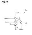
- Fig. 10 is a circuit diagram showing another construction of the pixel section P m,n of the photo-detecting apparatus 1 according to the first embodiment.
- the pixel section P m,n shown in the drawing further comprises an interrupting transistor T 5 in addition to the construction shown in Figs. 4 and 6.
- the interrupting transistor T 5 is provided between the photodiode PD and transferring transistor T 5 , and a voltage value as likely operative in a saturation region is applied to the gate electrode thereof.
- a voltage value as likely operative in a saturation region is applied to the gate electrode thereof.
- Fig. 11 is a timing chart for explaining an example in operation of the photo-detecting apparatus 1 according to the first embodiment. This figure shows a range of times for reading out the respective data of each pixel section P 1,n at 1st row and each pixel section P 2,n at 2nd row.
- each shown are a discharge control signal S reset,m at m-th row inputted to the gate terminal of the discharging transistor T 3 of each pixel section P m,n, a transmission control signal S trans inputted at the gate terminal of the transmitting transistor T 2 of each pixel section P m,n, a selection control signal S select,1 at 1 st row inputted to the gate terminal of the selecting transistor T 4 of the pixel section P 1,n at 1st row, and a selection control signal S select,2 at 2nd row inputted to the gate terminal of the selecting transistor T 4 of the pixel section P 2,n at 2nd row.
- each shown are a first input control signal S input,1 inputted to the gate terminal of a transistor T 11 of a first holding section H n,1 of each voltage holding section H n , a second input control signal S input2 inputted to the gate terminal of a transistor T 21 of a second holding section H n,2 of each voltage holding section H n, an output control signal S output,1 at 1st column inputted to each gate terminal of the transistors T 12 and T 22 of a voltage holding section H 1 at 1st column, an output control signal S output,N at N-th column inputted to each gate terminal of the transistors T 12 and T 22 of a voltage holding section H N at N-th column, and a first output value V 1,m,n outputted from the first pixel data readout section 20.
- each shown are a feeding operation of a bias potential V bias of each switch SW n , a transmitting operation of an electric charge of each switch SW n , opening/closing of a switch SW of each integrating circuit 31 n , opening/closing of a switch SW 1,1 at 1st column, opening/closing of a switch SW 1,N at N-th column, a second voltage value V 2,m,n outputted from the second data readout section 30, and a digital value D m,n outputted from the data output section 40.
- a discharge control signal S reset,m , a transmission control signal S trans , and a selection control signal S select,n at n-th row inputted to each pixel section P m,n each are a low level.
- a first input control signal S input,1 , a second input control signal S input,2 , and an output control signal S output,n at n-th column inputted to each voltage holding section H n of the first pixel data readout section 20 each are a low level.
- a readout of data of each pixel section P 1,n at 1st row is carried out during the period from the time t 10 to the time t 20 .
- the discharge control signal S reset,m is turned to a high level at the time t 10 , and then turned to a low level at the time t 11 that is later than the time t 10 .
- the transmission control signal S trans is turned to a high level at the time t 12 later than the time t 11 , and turned to a low level at the time t 13 later than the time t 12 .
- the selection control signal S select,1 at 1 st row is turned to a high level at the time t 10 .
- the switch SW n supplies the bias potential V bias to each pixel section P m,n during the period from the time t 10 to the time t 11 .
- the first input control signal S input,1 is kept at a high level only during a constant period of time that extends from the time t 11 when the discharge control signal S reset,m is turned to a low level till the time t 12 turned to a low level.
- a voltage value (dark signal component) outputted from the pixel section P 1,n to a wiring L 1,n is held by the first voltage holding section H n,1 of the voltage holding section H n .
- the second input control signal S input,2 keeps a high level only during a constant period of time from the time t 12 when the transmission control signal S trans is a high level till the time t 13 .
- a voltage value (bright signal component) outputted from the pixel section P 1,n to the wiring L 1,n is held by the second voltage holding section H n,2 of the voltage holding section H n .
- output control signals S output,1 to S output,N each are sequentially maintained only during a constant period of time.
- the output control signal S output,n at n-th column is kept at a high level
- the dark signal component and bright signal component of the pixel section P 1,n at 1 st row and n-th column held in the voltage holding section H n are outputted from the voltage holding section H n
- a difference between these dark signal component and bright signal component is determined by the subtracting circuit S, and a first voltage value V 1,1,n corresponding to intensity of light incident on the pixel section P 1,n is outputted from the first pixel data readout section 20.
- first voltage values V 1,1,1 to V 1,1,n corresponding to respective intensities of light incident on the N pixel sections P 1,1 to P 1,N at 1st row are sequentially outputted from the first pixel data readout section 20.
- the level of each voltage value V 1,1,n outputted during this period of time is a level corresponding to intensity of light incident on the pixel section P 1,n , generally different depending on the n value.
- the selection control signal S select,1 at 1st row is turned to a low level. In the aforementioned manner, data readout at each pixel section P 1,n at 1st row is completed.
- each pixel section P 2,n data readout of each pixel section P 2,n is carried out.
- the discharge control signal S reset,m is turned to a high level at the time t 20 , and turned to a low level at the time t 21 later than the time t 20 .
- the transmission control signal S trans is turned to a high level at the time t 22 later than the time t 21 , and turned to a low level at the time t 23 later than the time t 22 .
- the switch SW n supplies the bias potential V bias to each pixel section P m,n during the period from the time t 20 to the time t 21 .
- the first input control signal S input,1 is kept at a high level only during a constant period of time that extends from the time t 21 when the discharge control signal S reset,m is turned till a high level to the time t 22 turned to a high level.
- the voltage value (dark signal component) outputted from the pixel section P 2,n to the wiring L 1,n is held by the first voltage holding section H n,1 of the voltage holding section H n .
- the second input control signal S input , 2 keeps a high level only during a constant period of time from the time t 22 when the transmission control signal S trans is a high level till the time t 23 .
- a voltage value (bright signal component) outputted from the pixel section P 2,n to the wiring L 1,n is held by a second voltage holding section H n,2 of the voltage holding section H n .
- output control signals S output,1 to S output,N each are sequentially maintained only during a constant period of time.
- the output control signal S output,n at n-th column is kept at a high level
- the dark signal component and bright signal component of the pixel section P 2,n at 2nd row and n-th column held in the voltage holding section H n are outputted from the voltage holding section H n
- a difference between these dark signal component and bright signal component is determined by the subtracting circuit S, and a first voltage value V 1,2,n corresponding to intensity of light incident on the pixel section P 2,n is outputted from the first pixel data readout section 20.
- first voltage values V 1,2,1 to V 1,2,N corresponding to respective intensities of light incident on the N pixel sections P 2,1 to P 2,N at 2nd row are sequentially outputted from the first pixel data readout section 20.
- the level of each voltage value V 1,2,n outputted during this period of time is a level corresponding to intensity of light incident on the pixel section P 2,n , generally different depending on the n value.
- the selection control signal S select,2 at 2nd row is turned to a low level. From the above, data readout at each pixel section P 2,n at 2nd row is completed.
- first voltage values V 1,m,1 to V 1,m,N corresponding to intensities of light incident on the N pixel sections P m,1 to P m,N at each row are sequentially outputted from the first pixel data readout section 20.
- readout of the second voltage value V 2,m,n will be carried out as follows.
- the second pixel data readout section 30 operates as follows. During the period from the time t 10 to the time t 11 , the switch SW of each integrating circuit 31 n is closed, and the capacitive element C of each integrating circuit 31 n is discharged.
- a second voltage value V 2,1,n corresponding to the amount of the electric charge accumulated in the capacitive element C of the integrating circuit 31 n is outputted from the second pixel data readout section 30.
- second voltage values V 2,1,1 to V 2 , 1 , N corresponding to intensities of light incident on the respective N pixel sections P 1,1 to P 1,N at 1st row are sequentially outputted from the second pixel data readout section 30. From the above, data readout of each pixel section P 1,n at 1 st row is completed.
- the switch SW of each integrating circuit 31 n is closed, and the capacitive element C of each integrating circuit 31 n is discharged.
- the discharge control signal S reset,m is once turned to a high level, and then turned to a low level; simultaneously, each switch SW n is closed, and the electric charge accumulated in the capacitance section of the pixel section P 2,n at 2nd row is moved to the capacitive element C of the integrating circuit 31 n .
- each switch SW 1,n is sequentially closed for a constant period of time.
- a second voltage value V 2,2,n corresponding to the amount of the electric charge accumulated in the capacitive element C of the integrating circuit 31 n is outputted from the second pixel data readout section 30.
- second voltage values V 2,2,1 to V 2,2,N corresponding to intensities of light incident on the respective N pixel sections P 2,1 to P 2,N at 2nd row are sequentially outputted from the second pixel data readout section 30. From the above, data readout of each pixel section P 2,n at 2nd row is completed.
- the data output section 40 operates as follows. During the period from the time t 14 to the time t 15 , the first voltage value V 1,1,n on the pixel section P 1,n at 1st row read out from the first pixel data output section 20 is sequentially inputted to the data output section 40, and the second voltage value V 2,1,n on the pixel section P 1,n at 1st row read out from the second pixel data output section 30 is sequentially inputted to the data output section 40, and then the digital value D 1,n that is an A/D converted result of the first voltage value V 1,1,n or second voltage value V 2,1,n is sequentially outputted from the data output section 40.
- the first voltage value V 1,2,n on the pixel section P 2,n at 2nd row read out from the first pixel data output section 20 is sequentially inputted to the data output section 40
- the second voltage value V 2,2,n on the pixel section P 2,n at 2nd row read out from the second pixel data output section 30 is sequentially inputted to the data output section 40
- the digital value D 2,n that is an A/D converted result of the first voltage value V 1,2,n or second voltage value V 2,2,n is sequentially outputted from the data output section 40.
- the photo-detecting apparatus 1 can detect the intensity of incident light with high sensitivity and wide dynamic range.
- the second pixel data readout section 30 processes the output electric charge from the pixel section P m,n at m-th row.
- the second pixel data readout section 30 may be set to process the output electric charge from the pixel section at P m,n at another row.
- the second pixel data readout section 30 may be set to process the output electric charge from the pixel section P m,n at m-th row.
- the first pixel data readout section and second pixel data readout section operate in parallel with each other, it is possible to carry out an image pickup without lowering a frame rate.
- the discharge control signal S reset,m at m-th row inputted to the pixel section P m,n at m-th row is individually set, and the first voltage value V 1,m,n of the pixel section P m,n at m-th row outputted previously from the first pixel data readout section 20 is stored till the second voltage value V 2,m,n of the pixel section P m,n at m-th row is outputted from the second pixel data readout section 30.
- FIG. 12 is schematic diagram of the photo-detecting apparatus 2 according to the second embodiment.
- the photo-detecting apparatus 2 according to the second embodiment is different in the points of: including a second pixel data readout section 30A in place of the second pixel data readout section 30; including a data output section 40A in place of the data output section 40; and including a timing control section 50A in place of the timing control section 50.
- the second pixel data readout section 30A outputs not only a second voltage value V 2,m,n but also a third voltage value V 3,m,n to the data output section 40.
- the second voltage value V 2,m,n is a value having a linear relationship with respect to the amount of the electric charge generated at the photodiode PD within the pixel section P m,n .
- the third voltage value V 3,m,n is a value corresponding to a logarithmic value of the amount of the electric charge generated at the photodiode PD within the pixel section P m,n and flown in the second pixel data readout section 30A.
- the second voltage value V 2,m,n and third voltage value V 3,m,n outputted from the second pixel data readout section 30A may be outputted at different timings from each other, and inputted to the data output section 40A by way of a common wiring. Additionally, the second voltage value V 2,m,n and third voltage value V 3,m,n outputted from the second pixel data readout section 30A may be inputted to the data output section 40A by way of different wirings from each other.
- Fig. 13 is a schematic diagram of the second pixel data readout section 30A of the photo-detecting apparatus 2 according to the second embodiment.
- the second pixel data readout section 30A in the second embodiment shown in Fig. 13 is different in the points of including further a logarithmic compressing circuit 32 n provided in shunt with respect to an integrating circuit 31 n .
- Fig. 14 is a circuit diagram of each of the pixel section P m,n , integrating circuit 31 n , logarithmic compressing circuit 32 n and switch SW n of the photo-detecting apparatus 2 according to the second embodiment.
- the logarithmic compressing circuit 32 n is provided in parallel with the capacitive element C of the integrating circuit 31 n .
- the logarithmic compressing circuit 32 n has a transistor T 32 and a switch SW 32 .
- the source terminal of the transistor T 32 is connected to the input terminal of an amplifier A via a switch SW 32 .
- the drain terminal of the transistor T 32 is directly connected to the gate of the transistor T 32 , and also connected to the output terminal of the amplifier A.
- the logarithmic compressing circuit 32 n can output a third voltage value V 3,m,n corresponding to a logarithmic value of the inflow of the inputted electric charge.
- a transmission control signal S trans applied to the gate terminal of the transmitting transistor T 2 in the pixel section P m,n is a high level
- a discharge control signal S reset,m at m-th row applied to the gate terminal of the discharging transistor T 3 also is a high level
- the switch SW n connects a wiring L 2,n to the input terminal of the amplifier A, and that the switch SW in the integrating circuit 31 n is opened, and that the switch SW 32 in the logarithmic compressing circuit 32 n is closed.
- the third voltage value V 3,m,n outputted from the logarithmic compressing circuit 32 n is expressed by the following equation (1): where k is the Boltzmann's constant, T is the absolute temperature, q is the charge of electron, and I is a constant,
- V 3 , m , n ( k T / q ) ln ( I s h / I )
- the second pixel data readout section 30A outputs not only the second voltage value V 2,m,n corresponding to the amount of the electric charge generated at the photodiode PD within the pixel section P m,n and accumulated in the capacitive element C, but also the third voltage value V 3,m,n corresponding to the logarithmic value of the amount of the electric charge from the logarithmic compressing circuit 32 n . Also, the second pixel data readout section 30A outputs the second voltage value V 2,m,n and third voltage value V 3,m,n at timings different from each other to a common wiring leading to the data output section 40A.
- Fig. 15 is a diagram showing one constructional example of the data output section 40A of the photo-detecting apparatus 2 according to the second embodiment.
- the data output section 40A shown in this drawing has a substantially similar construction to that shown in Fig. 7, and A/D converting circuits 41 1 , 41 2 and a selecting output section 42.
- the A/D converting circuit 41 2 inputs the second voltage value V 2,m,n outputted from the second pixel data readout section 30A to be A/D converted, and outputs the second digital value D 2,m,n corresponding to the second voltage value V 2,m,n, and also inputs the third voltage value V 3,m,n outputted from the second pixel data readout section 30A to be A/D converted, and outputs the third digital value D 3,m,n corresponding to the third voltage value V 3,m,n .
- the selecting output section 42 inputs these first digital value D 1,m,n , second digital value D 2,m,n , and third digital value D 3,m,n ; based on results comparing in magnitude the first digital value D 1,m,n and a reference value, any one of the first digital value D 1,m,n , second digital value D 2,m,n , and third digital value D 3,m,n is selected, and the selected value is outputted as the digital value D m,n .
- the second digital value D 2,m,n or third digital value D 3,m,n and the reference value may be compared, and any one of the first voltage value V 1,m,n, second voltage value V 2,n,n, and third voltage value V 3,m,n may be compared in magnitude to the reference value.
- the reference value employed are two of a first reference value enable to determine whether the parasitic capacitance section of the pixel section P m,n is saturated or not, and a second reference value enable to determine whether the capacitive element C of the integrating circuit 31 n is saturated or not.
- the first digital value D 1,m,n (that is, an A/D converted result of the first voltage value V 1,m,n outputted from the selecting transistor T 4 of the pixel section P m,n and read out from the first pixel data readout section 20) is outputted from the data output section 40A as the digital value D m,n, thereby enabling photodetection with high sensitivity.
- the second digital value D 2,m,n (that is, an A/D converted result of the second voltage value V 2,m,n outputted from the discharging transistor T 3 of the pixel section P m,n and read out from the integrating circuit 31 n of the second pixel data readout section 30A) is outputted from the data output section 40A as the digital value D m,n , thereby enabling photodetection with wide dynamic range.
- the photo-detecting apparatus 2 can carry out an image pickup with high sensitivity and further wide dynamic range.
- Fig. 16 is a diagram showing another construction example of the data output section 40A of the photo-detecting apparatus 2 according to the second embodiment.
- the data output section 40A shown in this drawing has a substantially similar construction to that shown in Fig. 8, and a selecting output section 43 and an A/D converting circuit 44.
- the selecting output section 43 inputs the first voltage value V 1,m,n outputted from the first pixel data readout section 20, and inputs the second voltage value V 2,m,n and third voltage value V 3,m,n outputted from the second pixel data readout section 30A, and based on results comparing in magnitude the first voltage value v 1,m,n and the reference value, selects any one of the first voltage value V 1,m,n , second voltage value V 2,m,n and third voltage value V 3,m,n to be outputted.
- the second voltage value V 2,m,n or third voltage value V 3,m,n and the reference value may be compared.
- a first reference value enable to determine whether the parasitic capacitance section of the pixel section P m,n is saturated or not
- a second reference value enable to determine whether the capacitive element C of the integrating circuit 31 n is saturated or not.
- the photo-detecting apparatus 2 can carry out an image pickup with high sensitivity and further wide dynamic range.
- Fig. 17 is a timing chart for explaining an operation example of the photo-detecting apparatus 2 according to the second embodiment. This figure shows a range of time for reading out the data of each pixel section P 1-n at 1st row. As compared with the timing chart in the case of the first embodiment shown in Fig. 11, in the timing chart in the case of the second embodiment shown in Fig.
- the operation of the photo-detecting apparatus 2 according to the second embodiment from the time t 10 or before to the time t 15 is similar to that of the first embodiment. Note that the switch SW 32 of each logarithmic compressing circuit 32 n is opened in this period of time.
- the switch SW of each integrating circuit 31 n is closed for a given period of time, and the capacitive element C of each integrating circuit 31 n is discharged.
- the switch SW 32 of each logarithmic compressing circuit 32 n is closed; the discharge control signal S reset,m and transmission control signal S trans is turned to a high level, and simultaneously each switch SW n is closed, and the electric charge generated at the photodiode PD is flown in each logarithmic compressing circuit 32 n .
- each switch SW 1,n is sequentially closed for a given period of time.
- the third voltage value V 3,1,n corresponding to the logarithmic value of the amount of the electric charge flown in the logarithmic compressing circuit 32 n is outputted from the second pixel data readout section 30A.
- the third voltage values V 3,1,1 to V 3,1,N corresponding to the logarithmic values of the intensities of light incident on respective N pixel sections P 1,1 to P 1,N at 1 st row are sequentially outputted from the second pixel data readout section 30A.
- the digital value D 1,n that is a result in which any one of the first voltage value V 1,1,n , second voltage value V 2,1,n , and third voltage value V 3,1,n is A/D converted is sequentially outputted from the data output section 40A.
- the data holding section for holding the first voltage value V 1,1,n and second voltage value V 2,1,n (or these A/D converted results) outputted in advance is provided.
- the photo-detecting apparatus 2 can detect the intensity of incident light with high sensitivity and wide dynamic range.
Abstract
Description
- The present invention relates to a photo-detecting apparatus having a pixel section of an active-pixel type including a photodiode.
- A photo-detecting apparatus using CMOS technology is known; especially, the one of an active-pixel type system is known (see Patent Reference 1). The photo-detecting apparatus of the active-pixel system has a picture element or pixel section of an active-pixel type including a photodiode for generating the amount of an electric charge corresponding to intensity of incident light, and converts the electric charge generated at the photodiode into a voltage, namely carries out charge-to-voltage conversion by way of a source follower circuit constituting transistors, which enables photodetection with high sensitivity and low noise.
- An output voltage value V is represented by the following equation: V = Q/Cf, where Cf is the capacitance value of the parasitic capacitance section that stores the electric charge generated at the photodiode, and Q is the amount of the electric charge. As is apparent from this equation, when the capacitance value Cf is decreased, sensitivity of the photodetection can be enhanced.
- On the other hand, an upper limit of the output voltage value V is a level of several voltages due to the range of an applicable voltage of a power source and circuit-based restrictions. Thus, there is also an upper limit in the amount Q of the electric charge that can be accumulated in the parasitic capacitance section.
- Provided that the upper limit of the amount Q of the electric charge that can be accumulated in the parasitic capacitance section (the amount of saturated electric charge) is enhanced, it is assumed to increase the capacitance value Cf, or a voltage value of the power source. However, in order to increase the capacitance value Cf of the parasitic capacitance section, it is necessary to be manufactured through fine CMOS processes, so that a smaller voltage value of the power source is necessary; after all, it is impossible to increase the amount of the saturated electric charge. Additionally, if the capacitance value Cf of the parasitic capacitance section is increased, an important advantage of high sensitivity may be lost.
Patent Reference 1: JP-A-11-274454 - After studying a conventional photo-detecting apparatus in detail, the inventors et al. find out the following problems. That is, though the conventional photo-detecting apparatus can perform photodetection with high sensitivity, there is a problem that the dynamic range of the photodetection is narrowed due to restrictions of the amount of saturated electric charge.
- The present invention is made to solve the aforementioned problem, and it is an object to provide a photo-detecting apparatus having a structure which enables photodetection with high sensitivity and wide dynamic range.
- A photo-detecting apparatus according to the present invention is characterized by comprising: (1) a pixel section including a photodiode for generating an electric charge of the amount corresponding to intensity of incident light, an amplifying transistor for outputting a voltage value corresponding to the amount of the electric charge accumulated in a parasitic capacitance section formed at its gate terminal, a transmitting transistor for transmitting the electric charge generated at the photodiode to the gate terminal of the amplifying transistor, a discharging transistor for initializing the electric charge of the parasitic capacitance section, and a selecting transistor for outputting selectively the voltage value outputted from the amplifying transistor; (2) a first pixel data readout section for reading out the voltage value outputted from the selecting transistor of the pixel section and outputting a first voltage value corresponding to the voltage value; (3) a connection switching section, having a first terminal connected to the discharging transistor of the pixel section, a second terminal for inputting a bias potential for initializing the electric charge of the gate terminal of the amplifying transistor of the pixel section, and a third terminal, for making an electrical connection between the first terminal and second terminal, or between the first terminal and third terminal; and (4) a second pixel data readout section, of which the input terminal is connected to the third terminal of the connection switching section, and which includes a capacitive element having a larger capacitance value than that of the parasitic capacitance section, for accumulating in the capacitive element the electric charge flown from the third terminal of the connection switching section to the input terminal, and for outputting a second voltage value corresponding to the amount of the accumulated electric charge.
- In this photo-detecting apparatus, when light is incident on the pixel section, the amount of the electric charge corresponding to intensity of incident light is generated at the photodiode included in the pixel section, and the electric charge is accumulated in the parasitic capacitance section. The voltage value corresponding to the amount of the electric charge accumulated at the parasitic capacitance section is outputted from the pixel section by way of the amplifying transistor and selecting transistor, and reads out from the first data readout section. Then, the first voltage value corresponding to this readout voltage value is outputted from the first pixel data readout section. When the parasitic capacitance section is not saturated, that is, when the intensity of incident light on the pixel section is comparatively small, the first voltage value represents with high precision a result where the intensity of incident light is detected with high sensitivity.
- Further, the electric charge generated at the photodiode included in the pixel section is outputted from the pixel section via the discharging transistor, and inputted to the second pixel data readout section via connection switching means. In the second pixel data readout section, the electric charge flown therein is accumulated in the capacitive element, and the second voltage value corresponding to the amount of the accumulated electric charge is outputted. In this case, the capacitance value of the capacitive element included in the second pixel data readout section is larger than that of the parasitic capacitance section included in the pixel section. Thus, when the parasitic capacitance section is saturated, that is, even when the intensity of incident light on this pixel section is comparatively large, this second voltage value represents with high precision a detected result of the intensity of incident light.
- Therefore, according to the photo-detecting apparatus, based on the first voltage value outputted from the first pixel data readout section and the second voltage value outputted from the second pixel data readout section, photodetection can be carried out with high sensitivity and wide dynamic range.
- Here, it is preferred that the capacitance value of the capacitive element included in the second data readout section is 2K times as large as that of the parasitic capacitance section, where K is an integer of 1 or more. In this case, when the parasitic capacitance section of the pixel section is not saturated, the second voltage value outputted from the second pixel data readout section can become 1/2K times as small as the first voltage value outputted from the first pixel data readout section. Then, for example, post-processes such as determination whether the parasitic capacitance section of the pixel section is saturated or not, selection of either of the first voltage value and second voltage value, and A/D conversion to both or either of the first voltage value and second voltage value may be facilitated.
- It is preferred that in the photo-detecting apparatus according to the invention, the photodiode included in the pixel section has a second semiconductor region of a second conduction-type on a first semiconductor of a first conduction-type, has a third semiconductor region of the first conduction-type on the second semiconductor region, a pn junction is formed between the first semiconductor region and second semiconductor region, and a pn junction is formed between the second semiconductor region and third semiconductor region. Thus, when the photodiode is the one of a buried type, photodetection with further high sensitivity can be performed. Here, one of the first conduction-type and second conduction-type means n-type, while the other thereof means p-type.
- It is preferred that the photo-detecting apparatus according to the present invention further includes an interrupting transistor used in a saturation region, while the pixel section is provided between the photodiode and transmitting transistor. Also in this case, photodetection with further high sensitivity can be performed.
- It is preferred that the photo-detecting apparatus according to the present invention has a plurality of pixel sections arranged two-dimensionally. In this case, a two-dimensional image can be picked up.
- In addition, though the second pixel data readout section may have one capacitive element for each of all the two-dimensionally arranged pixel sections, it preferably has one capacitive element for each column. In the latter case, the electric charge generated at the photodiode included in each pixel section provided in one row can be simultaneously outputted by way of the discharging transistor of the pixel section, inputted to the second pixel data readout section by way of the connection switching means, and accumulated in the corresponding capacitive element provided for each column. Thus, this manner can perform an image pickup at high speed.
- Additionally, it is preferred that during the period when the first pixel data readout section processes the voltage value outputted from a pixel section of a certain row, the second pixel data readout section processes the electric charge outputted from the pixel section of the corresponding row. Alternatively, it is preferred that during the period when the first pixel data readout section processes the voltage value outputted from a pixel section of a certain row, the second pixel data readout section processes the electric charge outputted from the pixel section of another row. In this way, when the first pixel data readout section and second pixel data readout section operate in parallel, an image pickup can be carried out without lowering a frame rate.
- It is preferred that the photo-detecting apparatus according to the present invention further comprises an A/D converting section for inputting the first voltage value outputted from the first pixel data readout section to be A/D converted, and outputting the first digital value corresponding to the first voltage value, and for inputting the second voltage value outputted from the second pixel data readout section to be A/D converted, and outputting the second digital value corresponding to the second voltage value. Additionally, it is preferred that the photo-detecting apparatus further comprises a selecting output section for inputting the first digital value and second digital value outputted from the A/D converting section, and selecting and outputting either of the first digital value and second digital value, based on a result where any one of the first voltage value, second voltage value, first digital value and second digital value is compared in magnitude to a reference value.
- In this case, by means of the A/D converting section, the first voltage value outputted from the first pixel data readout section is A/D converted, and the first digital value corresponding to the first voltage value is outputted, while the second voltage value outputted from the second pixel data readout section is A/D converted, and the second digital value corresponding to the second voltage value is outputted. Then, by means of the selecting output section, based on a result where any one of the first voltage value, second voltage value, first digital value and second digital value is compared in magnitude to a reference value, one of the first digital value and second digital value is selected and outputted.
- Alternatively, it is preferred that the photo-detecting apparatus further comprises an A/D converting section for inputting a first voltage value outputted from the first pixel data readout section and a second voltage value outputted from the second pixel data readout section, and selecting and outputting either of the first voltage value and second voltage value, based on a result where either of the first voltage value and second voltage value is compared in magnitude to a reference value. Additionally, it is preferred that the photo-detecting apparatus further comprises an A/D converting section for inputting the voltage value outputted from the selecting output section to be A/D converted, and outputting a digital value corresponding to the voltage value.
- In this case, by means of the selecting output section, based on a result where either of the first voltage value and second voltage value is compared in magnitude to a reference value, one of the first voltage value and second voltage value is selected and outputted. Then, by means of the A/D converting section, the voltage value outputted from the selecting output section is A/D converted, and the digital value corresponding to the voltage value is outputted.
- It is preferred that in the photo-detecting apparatus according to the present invention, the second pixel data readout section further includes a logarithmic compressing circuit arranged in parallel to the capacitive element, and inputs in the logarithmic compressing circuit the electric charge flown from the third terminal of the connection switching section in the input terminal, and then outputs a third voltage value corresponding to a logarithmic value of the in-flow amount of the inputted electric charge. In this case, from the second pixel data readout section, not only the second voltage value corresponding to the amount of the electric charge generated at the photodiode included in the pixel section be outputted, but also the third voltage value corresponding to the logarithmic value of the in-flow amount of the electric charge is outputted from the logarithmic compressing circuit. Therefore, based on the first voltage value outputted from the first pixel data readout section and the second voltage value and third voltage value outputted from the second pixel data readout section, photodetection can be performed with high sensitivity and wide dynamic range.
- Thus, when the second pixel data readout section also includes the logarithmic compressing circuit, it is preferred that the photo-detecting apparatus further comprises an A/D converting section for inputting the first voltage value outputted from the first pixel data readout section to be AID converted, and outputting the first digital value corresponding to the first voltage value, and for inputting the second voltage value and third voltage value outputted from the second pixel data readout section to be A/D converted, and outputting the second digital value corresponding to the second voltage value and the third digital value corresponding to the third voltage value. Additionally, it is preferred that the photo-detecting apparatus further comprises a selecting output section for inputting the first digital value, second digital value, and third digital value outputted from the A/D converting section, and outputting any one of the first digital value, second digital value, and third digital value, based on a result where any one of the first voltage value, second voltage value, third voltage value, first digital value, second digital value, and third digital value is compared in magnitude to a reference value.
- Alternatively, it is preferred that the photo-detecting apparatus further comprises a selecting output section for inputting the first voltage value outputted from the first pixel data readout section, and the second voltage value and third voltage value outputted from the second pixel data readout section, and for outputting any one of the first voltage value, second voltage value, and third voltage value, based on a result where any one of the first voltage value, second voltage value, and third voltage value is compared in magnitude to a reference value.
- In accordance with the invention, photodetection with high sensitivity and wide dynamic range becomes possible.
- Fig. 1 is a diagram showing a schematic construction of a first embodiment of a photo-detecting apparatus according to the present invention;
- Fig. 2 is a diagram showing a construction of a photo-detecting section in the photo-detecting apparatus according to a first embodiment;
- Fig. 3 is a diagram showing a construction of a first pixel data readout section in the photo-detecting apparatus according to the first embodiment;
- Fig. 4 is a circuit diagram of each of a pixel section Pm,n, a voltage holding section Hn, and a switch SWn in the photo-detecting apparatus according to the first embodiment;
- Fig. 5 is a diagram showing a construction of a second pixel data readout section in the photo-detecting apparatus according to the first embodiment;
- Fig. 6 is a circuit diagram of each of a pixel section Pm,n, an integration section 31n, and a switch SWn in the photo-detecting apparatus according to the first embodiment;
- Fig. 7 is a diagram showing one construction example of a data output section in the photo-detecting apparatus according to the first embodiment;
- Fig. 8 is a diagram showing another construction example of the data output section in the photo-detecting apparatus according to the first embodiment;
- Fig. 9 is a diagram showing a sectional structure of the pixel section Pm,n in the photo-detecting apparatus according to the first embodiment;
- Fig. 10 is a circuit diagram showing another construction of the pixel section Pm,n in the photo-detecting apparatus according to the first embodiment;
- Fig. 11 is a timing chart for explaining an operation example of the photo-detecting apparatus according to the first embodiment;
- Fig. 12 is a diagram showing a schematic construction of a second embodiment of the photo-detecting apparatus according to the present invention;
- Fig. 13 is a diagram showing a construction of a second pixel data readout section in the photo-detecting apparatus according to the second embodiment;
- Fig. 14 is a circuit diagram of each of a pixel section Pm,n, an integrating circuit 31n, a logarithmic compressing circuit 32n, and a switch SWn in the photo-detecting apparatus according to the second embodiment;
- Fig. 15 is a diagram showing one construction example of a data output section in the photo-detecting apparatus according to the second embodiment;
- Fig. 16 is a diagram showing another construction example of the data output section in the photo-detecting apparatus according to the second embodiment; and
- Fig. 17 is a timing chart for explaining an operation example of the photo-detecting apparatus according to the second embodiment.
- 1, 2...photo-detecting apparatus; 10...photo-detecting section; 20...first pixel data readout section; 30, 30A...econd pixel data readout section; 40, 40A...data output section; and 50, 50A...timing control section.
- In the following, the best modes for carrying out the inventions will be explained in detail with reference to Figs. 1 to 17. In the explanation of the drawings, the same elements will be denoted by the same reference symbols and these redundant descriptions will be omitted. In addition, M and N are integers of 2 or more; m is an arbitrary integer of 1 or more and M or less, and n is an arbitrary integer of 1 or more and N or less, as far as these are not specifically defined.
- The summary of the whole construction of a photo-detecting
apparatus 1 according to a first embodiment will be first explained with reference to Figs. 1 and 2. - Fig. 1 is a schematic diagram of the photo-detecting
apparatus 1 according to the first embodiment. Fig. 2 is a diagram of a photo-detectingsection 10 of the photo-detectingapparatus 1 according to the first embodiment. The photo-detectingapparatus 1 shown in these figures is composed of the photo-detectingsection 10, a first pixeldata readout section 20, a second pixeldata readout section 30, adata output section 40, atiming control section 50 and switches SW1 to SWn. It is preferred that these components are formed on a common semiconductor substrate. In the case, it is preferred that a layout on the substrate is the same one as depicted in these figures. Here, thetiming control section 50 may be divided into a plurality of parts and arranged apart from each other on the substrate, though it is schemed to control the whole operation of the photo-detectingapparatus 1. - The photo-detecting
section 10 has MxN pixel sections Pm,n that are two-dimensionally arranged by M rows and N columns. Each pixel section Pm,n is positioned at m-th row and n-th column. Each pixel section Pm,n has a common construction, which is the one of an active-pixel type including a photodiode, and outputs a voltage value corresponding to intensity of light incident on the photodiode to a wiring L1,n. Each wiring L1,n is commonly connected to the output ends of M pixel sections P1,n to PM,n, while each wiring L2,n is commonly connected to the other ends of M pixel sections P1,n to PM,n that are located at n-th column. - The first pixel
data output section 20 is connected to N wirings L1,1 to L1,N, and inputs a voltage value that is outputted from each pixel section Pm,n to the wiring L1,n, and outputs in sequence a first voltage value V1,m,n representing a pixel data after a predetermined processing is carried out. Each voltage value V1,m,n is a value corresponding to intensity of light incident on the pixel section Pm,n. Specifically, when the first voltage value V1,m,n represents a result detecting the intensity of the incident light with high sensitivity when a parasitic capacitance section of the pixel section Pm,n is not saturated, that is, when the intensity of the incident light on the pixel section Pm,n is relatively small. - The second pixel
data output section 30 is connected to N wirings L2,1 to L2,N through the switches SW1 to SWn, and inputs an electric charge that is outputted from each pixel section Pm,n to the wiring L2,n and flown therein through the switch SWn. The electric charge is accumulated in the capacitive element, and a second voltage value V2,m,n corresponding to the amount of the electric charge accumulated in the capacitive element is outputted in sequence. The capacitance value of the capacitive element included in the second pixeldata readout section 30 is larger than that of the parasitic capacitance section included in the pixel section Pm,n. Each voltage value V2,m,n is a value corresponding to intensity of light incident on the pixel section Pm,n. In addition, the second voltage value V2,m,n represents detected results of the intensity of the incident light with high precision when the parasitic capacitance section of the pixel section Pm,n is saturated, that is, when intensity of incident light on the pixel section Pm,n is comparatively strong. - The
data output section 40 inputs a first voltage value V1,m,n outputted from the first pixeldata readout section 20 and a first voltage value V2,m,n outputted from the second pixeldata readout section 30, and outputs a digital valued Dm,n after a predetermined processing is carried out. Each digital value Dm,n is a value as a result where either of the first voltage value V1,m,n and second voltage value V2,m,n is A/D converted, and represents intensity of light incident on the pixel section Pm,n. - The
timing control section 50 controls the operations of the photo-detectingsection 10, first pixeldata readout section 20, second pixeldata readout section 30,data output section 40, and switches SW1 to SWN, respectively. Thetiming control section 50 generates a variety of control signals at a given timing, for example, by a shift register circuit, and these control signals are transmitted to the photo-detectingsection 10, first pixeldata readout section 20, second pixeldata readout section 30,data output section 40 and switches SW1 to SWN, respectively. It is noted that in Figs. 1 and 2, drawings of wirings for transmitting the control signals are partially omitted. - The constructions of the photo-detecting
section 10 and first pixeldata readout section 20 of the photo-detectingapparatus 1 according to the first embodiment will next be explained with respect to Figs. 3 and 4. - Fig. 3 is a schematic diagram of the first pixel
data readout section 20 of the photo-detectingapparatus 1 according to the first embodiment. The first pixeldata readout section 20 has N voltage holding section H1 to HN, two voltage follower circuits F1, F2 and a subtracting circuit S. Each voltage holding section Hn has a common construction and is connected with a wiring L1,n, and inputs and holds a voltage value, which is outputted from each of M pixel sections P1,n to PM,n positioned at n-th column, to a wiring L1,n, and further can output the holding voltage value. The N voltage holding sections H1 to HN each output a voltage value in sequence. The voltage values held and outputted by each voltage holding section Hn are two voltage values Vn,1, Vn,2 outputted from the pixel section Pm,n at different times from each other. - The two voltage follower circuits F1, F2 each have a common construction; an inverting input terminal and an output terminal of an amplifier are directly connected to each other, to thus have a high input impedance and a low output impedance, ideally resulting in an amplifier having amplification factor of 1. In the one voltage follower circuit F1, the one voltage values Vn,1 outputted sequentially from the N voltage holding sections H1 to HN are inputted to a non-inverting input terminal. In the other voltage follower circuit F2, the other voltage values Vn,2 outputted sequentially from the N voltage holding sections H1 to HN are inputted to a non-inverting input terminal.
- The subtracting circuit S has an amplifier and four resistors R1 to R4. The inverting input terminal of the amplifier is connected to the output terminal of the voltage follower circuit F1 via the resistor R1, and connected to its own output terminal via the resistors R3. The non-inverting input terminal of the amplifier is connected to the output terminal of the voltage follower circuit F2 via the resistor R2, and connected to ground potential via the resistors R4. Assuming that the resistance values of the resistors R1 to R4 are equal to each other, where the amplification ratio of each of the voltage follower circuits F1, F2 is 1, the first voltage value V1,m,n outputted from the output terminal of the subtracting circuit S is expressed by the following equation: V1,m,n = Vn,2 - Vn,1.
- Fig. 4 is a circuit diagram of each of the pixel section Pm,n, voltage holding section Hn and switch SWn of the photo-detecting
apparatus 1 according to the first embodiment. In this drawing, one pixel section Pm,n, one voltage holding section Hn, and one switch SWn are representatively illustrated for simplicity. - Each pixel section Pm,n includes a photodiode PD for generating an electric charge of an amount of corresponding to intensity of incident light, an amplifying transistor T1 for outputting a voltage value of the amount of an electric charge accumulated in a parasitic capacitance section formed in its gate terminal, a transmitting transistor T for transmitting the electric charge generated at the photodiode to the gate terminal of the amplifying transistor T1, a discharging transistor T3 for initializing the electric charge of the parasitic capacitance section formed in the gate terminal of the amplifying transistor T1, and a selecting transistor T4 for outputting a voltage value outputted from the amplifying transistor T1 to an external wiring L1,n.
- In the photodiode PD, its anode terminal is set to ground potential. In the amplifying transistor T1, a parasitic capacitance section is formed in its gate terminal, and its drain terminal is set to a bias potential. In the transmitting transistor T2, its drain terminal is connected to the gate terminal of the amplifying transistor T1, and its source terminal is connected to the cathode terminal of the photodiode PD. In the discharging transistor T3, its source terminal is connected to the gate terminal of the amplifying transistor T1, and its drain terminal is connected to the switch SWn. In the selecting transistor T4, its source terminal is connected to the source terminal of the amplifying transistor T1 and its drain terminal is connected to the wiring L1,n. Additionally, a constant current source is connected to the wiring L1,n. The amplifying transistor T1 and selecting transistor T4 constitute a source follower circuit.
- Here, the constant current source may be connected to the wiring L1,n for each line to be arranged. For example, in a case where switches are respectively arranged between the wirings L1,n and the first pixel
data readout section 20, and where the first pixeldata readout section 20 reads out sequentially voltage values outputted from the respective N pixel sections Pm,1to Pm,N at m-th row in such a manner that these switches are closed sequentially, only one constant current source may be arranged between these switches and the first pixeldata readout section 20. - In the transmitting transistor T2, a transmission control signal Strans is inputted to its gate terminal, and when the transmission control signal Strans is a high level, the electric charge generated at the photodiode PD is transmitted to the parasitic capacitance section formed at the gate terminal of the amplifying transistor T1. In the discharging transistor T3, a discharge control signal Sreset,m at m-th row is inputted to its gate terminal, and when discharge control signal Sreset,m at m-th row is a high level, a low resistance is provided between the gate electrode of the amplifying transistor T1 and the switch SWn. In the selecting transistor T4, a selection control signal Sselect,m at m-th row is inputted to its gate terminal, and when the selection control signal Sselect,m at m-th row is a high level, a voltage value outputted from the amplifying transistor T1 is outputted to an external wiring L1,n.
- In the thus constructed pixel section Pm,n, the transmission control signal Strans is a low level, and the discharge control signal Sreset,m at m-th row is a high level; when a bias potential Vbias is inputted to the discharging transistor T3 via the switch SWn, the electric charge of the parasitic capacitance section of the gate terminal of the amplifying transistor T1 is initialized; when the selection control signal Sselect,m at m-th row is a high level, a voltage value (dark signal component) outputted from the amplifying transistor T1 put in an initialized state is outputted to the wiring L1,n via the selecting transistor T4. On the other hand, when the discharge control signal Sreset,m at m-th row is a low level, and the transmission control signal Strans and selection control signal Sselect,m at m-th row each are a high level, the electric discharge generated at the photodiode PD is inputted to the gate terminal of the amplifying transistor T1, and a voltage value (bright signal component) outputted from the amplifying transistor T1 corresponding to the amount of the electric discharge is outputted to the wiring L1,n via the selecting transistor T4.
- The voltage holding section Hn includes a first holding section Hn,1 and a second holding section Hn,2. The first holding section Hn,1 and second holding section Hn,2 have a similar construction to each other, and can input and hold voltage values outputted sequentially from the selecting transistor T4 of each of the M pixel sections P1,n to PM,n located at n-th column, and further output the held voltage value.
- The first holding section Hn,1 includes a transistor T11, a transistor T12, and a capacitive element C1. One terminal of the capacitive element C1 is set to ground potential, while the other terminal of the capacitive element C1 is connected to the drain terminal of the transistor T11 and the source terminal of the transistor T12. The source terminal of the transistor T11 is connected to the selecting transistor T4 of the pixel section Pm,n via the wiring L1,n. The drain terminal of the transistor T12 is connected to the voltage follower circuit F1. In the thus constructed first holding section Hn,1, when a first input control signal Sinput,1 inputted to the gate terminal of the transistor T11 is a high level, a voltage value outputted from the pixel section Pm,n connected via the wiring L1,n is held in the capacitive element C1, while when an output control signal Soutput,n inputted to the gate terminal of the transistor T12 is a high level, a voltage value Vn,1 held in the capacitive element C1 is outputted to the voltage follower circuit F1.
- The second holding section Hn,2 includes a transistor T21, a transistor T22, and a capacitive element C2. One terminal of the capacitive element C2 is set to ground potential, while the other terminal of the capacitive element C2 is connected to the drain terminal of the transistor T21 and the source terminal of the transistor T22. The source terminal of the transistor T21 is connected to the selecting transistor T4 of the pixel section Pm,n via the wiring L1,n. The drain terminal of the transistor T22 is connected to the voltage follower circuit F2. In the thus constructed second holding section Hn,2, when a second input control signal Sinput,2 inputted to the gate terminal of the transistor T21 is a high level, a voltage value outputted from the pixel section Pm,n connected via the wiring L1,n is held in the capacitive element C2, while when an output control signal Soutput,n inputted to the gate terminal of the transistor T22 is a high level, a voltage value Vn,2 held in the capacitive element C2 is outputted to the voltage follower circuit F2.
- The first holding section Hn,1 and second holding section Hn,2 each operate at a different timing from each other. For example, in the first holding section Hn,1, the transmission control signal Strans is a low level in the pixel section Pm,n connected via the wiring L1,n, and the discharge control signal Sreset,m at m-th row and selection control signal Sselect,m at m-th row each are a high level, the voltage value (dark signal component) Vn,1 outputted from the amplifying transistor T1 is inputted and held. On the other hand, in the second holding section Hn,2, the discharge control signal Sreset,m at m-th row in the pixel section Pm,n connected via the wiring L1,n is a low level, and the transmission control signal Strans and selection control signal Sselect,m at m-th row each are a high level, the voltage value (bright signal component) Vn,2 outputted from the amplifying transistor T1 is inputted and held.
- It should be noted that the transmission control signal Strans, discharge control signal Sreset,m at m-th row, selection control signal Sselect, m at m-th row, first input control signal Sinput,1, second input control signal Sinput,2, output control signal Soutput,n at n-th column each are outputted from the
timing control section 50. - The construction of the second pixel
data readout section 30 of the photo-detectingapparatus 1 according to the first embodiment will next be explained with reference to Figs. 5 and 6. - Fig. 5 is a schematic diagram of the second pixel
data readout section 30 of the photo-detectingapparatus 1 according to the first embodiment. The second pixeldata readout section 30 has N integrating circuits 31l to 31N, and N switches SWl,l to SWl,N. Each integrating circuit 31n has a common construction, and has a capacitive element for accumulating an electric charge flown in its input end from the switch SWn, and outputs a voltage value corresponding to the amount of the electric charge accumulated in this capacitive element to the switch SWl,n. The second pixeldata readout section 30 outputs a voltage value outputted from each of the N integrating circuits 31l to 31N as a second voltage value V2,m,n by closing sequentially the switches SWl,l to SWl,N. - Fig. 6 is a circuit diagram of the pixel section Pm,n, integrating circuit 31n, and switch SWn of the photo-detecting
apparatus 1 according to the first embodiment. In this drawing, one pixel section Pm,n, one integrating circuit 31n, and one switch SWn are representatively illustrated for simplicity. - Each integrating
circuit 31n has an amplifier A, a capacitive element C and a switch SW. The capacitive element C and switch SW each are arranged in parallel between the input and output terminals of the amplifier A. A capacitance value of this capacitive element C is larger than that of the parasitic capacitance section formed at the gate terminal of the amplifying transistor T1 of the pixel section Pm,n. Additionally, it is preferred that the capacitance value of the capacitive element C is 2K times as large as that of the parasitic capacitance section, where K is an integer of 1 or more. This integrating circuit 31n initializes the capacitive element C when the switch SW is closed. Also, the integrating circuit 31n accumulates in the capacitive element C the electric charge flown in its input terminal from the wiring L2,n via the switch SWn when the switch SW is opened, and outputs the voltage value corresponding to the amount of the electric charge accumulated in the capacitive element to the switch SW1,n. - Each switch SWn has a first terminal connected to the drain terminal of the discharging transistor T3 of the pixel section Pm,n, a second terminal connected to a bias potential Vbias to initialize the electric charge of the gate terminal of the amplifying transistor T1 of the pixel section Pm,n, and a third terminal connected to the input terminal of the integrating circuit 31n. Then, the switch SWn operates as a connection switching section to establish an electrical connection between the first terminal and second terminal, or between the first terminal and third terminal. When the electrical connection is made between the first terminal and second terminal of the switch SWn, the bias potential Vbias is supplied to the discharging transistor T3 of the pixel section Pm,n via the switch SWn. On the other hand, when the electrical connection is made between the first terminal and third terminal of the switch SWn, the electric charge generated at the photodiode of the pixel section Pm,n is moved to the input terminal of the integrating circuit 31n via the discharging transistor T3 and switch SWn.
- Note that a control signal to control each opening/closing operations of each of the switches SW, SWn, SWl,n is outputted from the
timing control section 50. Also, in the switch SWn, there is a state such that no electrical connections between the first terminal and second terminal, and between the first terminal and third terminal are established. - The construction of the
data output section 40 of the photo-detectingapparatus 1 according to the first embodiment will next be explained with reference to Figs. 7 and 8. - Fig. 7 is a diagram showing one constructional example of the
data output section 40 of the photo-detectingapparatus 1 according to the first embodiment. Thedata output section 40 shown in this drawing has A/D converting circuits 411, 412 and a selectingoutput section 42. The A/D converting circuits 411 inputs a first voltage value V1,m,n outputted from the first pixeldata readout section 20 to be A/D converted, and outputs a first digital value D1,m,n corresponding to the first voltage value V1,m,n. The A/D converting circuits 412 inputs a second voltage value V2,m,n outputted from the second pixeldata readout section 30 to be A/D converted, and outputs a second digital value D2,m,n corresponding to the second voltage value V2,m,n. - Here, corresponding to a fact that the capacitance value of the capacitive element C of each integrating circuit 31n is 2K times as large as that of the parasitic capacitance section of the pixel section Pm,n, the first digital value where the input voltage value to the A/D converting circuit 411 is one value V and a selecting
output section 42, and the second digital value where the input voltage value to the A/D converting circuit 412 is V/2K are equal to each other. - The selecting
output section 42 inputs the first digital value D1,m,n and second digital value D2,m,n, selects one of the first digital value D1,m,n and second digital value D2,m,n based on a result that compares in magnitude the first digital value D1,m,n with a reference value, and outputs the selected value as a digital value Dm,n. - Specifically, the reference value is set to a digital value corresponding to a saturation value of the first voltage value outputted from the first pixel
data readout section 20, or set to a digital value slightly smaller than this value. That is, when the first digital value D1,m,n and the reference value are compared in magnitude, it can be determined whether the parasitic section of the pixel section Pm,n is saturated or not. Then, when the first digital value D1,m,n is smaller than the reference value, the selectingoutput section 42 outputs the first digital value D1,m,n as a digital value Dm,n, while when the first digital value D1,m,n is the reference value or more, thesection 42 outputs the second digital value D2,m,n as a digital value Dm,n. - Here, instead of comparing the first digital value D1,m,n to the reference value, the second digital value D2,m,n may be compared in magnitude to the reference value, and the first voltage value V1,m,n or the second voltage value V2,m,n may be compared in magnitude to the reference value. In any one of these cases, the reference value is set to a value that can determine whether the parasitic section of the pixel section Pm,n is saturated or not.
- As mentioned above, when the parasitic capacitance section of the pixel section Pm,n is not saturated, that is, when intensity of incident light to the pixel section Pm,n is comparatively small, the first digital value D1,m,n (that is, an A/D converted result of the first voltage value V1,m,n outputted from the selecting transistor T4 of the pixel section Pm,n and read out from the first pixel data readout section 20) is outputted from the
data output section 40 as the digital value Dm,n, thereby enabling photodetection with high sensitivity. On the other hand, when the parasitic capacitance section of the pixel section Pm,n is saturated (or, when it is a status on the verge of saturation), that is, when the intensity of incident light on the pixel section Pm,n is comparatively greater, the second digital value D2,m,n (that is, an A/D converted result of the second voltage value V2,m,n outputted from the discharging transistor T3 of the pixel section Pm,n and read out from the second pixel data readout section 30) is outputted from thedata output section 40 as the digital value Dm,n, thereby enabling photodetection with wide dynamic range. Therefore, the photo-detectingapparatus 1 according to the first embodiment can carry out an image pickup with high sensitivity and wide dynamic range. - Fig.8 is a diagram showing another constructional example of the
data output section 40 of the photo-detectingapparatus 1 according to the first embodiment. Thedata output section 40 presented in this drawing has a selectingoutput section 43 and an A/D converting circuit 44. The selectingoutput section 43 inputs the first voltage value V1,m,n outputted from the first pixeldata readout section 20 and the second voltage value V2,m,n outputted from the second pixeldata readout section 30, selects one of the first voltage value V1,m,n and the second voltage value V2,m,n to be outputted, based on a result where the first voltage value V1,m,n and a reference value is compared in magnitude to each other. - Specifically, the reference value is set to a saturation value of the first voltage value V1,m,n outputted from the outputted from the first pixel
data readout section 20, or set to a slightly smaller value than this saturation value. Thus, it can be determined whether the parasitic capacitance section of the pixel section Pm,n is saturated or not by comparing in magnitude the first voltage value V1,m,n with the reference value. Then, the selectingoutput section 43 outputs the first voltage value V1,m,n when the first voltage value V1,m,n is smaller than the reference value, while it outputs the second voltage value V2,m,n when the first voltage value V1,m,n is the reference value or more. - Additionally, the second voltage value V2,m,n and the reference value may be compared in magnitude instead of making a comparison in magnitude between the first voltage value V1,m,n and the reference value. Also in this case, the reference value is set to a value capable of determining whether the parasitic capacitance section of the pixel section Pm,n is saturated or not.
- The A/
D converting circuit 44 inputs the voltage value outputted from the selectingoutput section 43 and outputs the digital value Dm,n corresponding to this voltage value. Specifically, corresponding to a situation that the capacitance value of the capacitive element C of each integrating circuit 31n is 2K times as large as that of the parasitic capacitance section of the pixel section Pm,n, when the A/D converting circuit 44 A/D converts the first voltage value V1,m,n outputted from the first pixeldata readout section 20, the digital value obtained from the A/D conversion is outputted as the digital value Dm,n, while when it converts the second voltage value V2,m,n outputted from the second pixeldata readout section 30, the digital value obtained from the A/D conversion is shifted to higher order bits by K bits and the resultant is outputted as the digital value Dm,n. - As mentioned above, when the parasitic capacitance section of the pixel section Pmn is not saturated, that is, when intensity of incident light on the pixel section Pm,n is comparatively small, an A/D converted result of the first voltage value V1,m,n outputted from the selecting transistor T4 of the pixel section Pm,n and read out by the first pixel
data readout section 20 is outputted from thedata output section 40 as the digital value Dm,n, thereby enabling photodetection with high sensitivity. On the other hand, when the parasitic capacitance section of the pixel section Pm,n is saturated (or when it is a status on the verge of saturation), that is, when the intensity of incident light on the pixel section Pm,n is comparatively great, an A/D converted result of the second voltage value V2,m,n outputted from the discharging transistor T3 of the pixel section Pm,n and read out from the second pixeldata readout section 30 is outputted from thedata output section 40 as the digital value Dm,n, thereby enabling photodetection with wide dynamic range. Therefore, the photo-detectingapparatus 1 according to the first embodiment can carry out an image pickup with high sensitivity and wide dynamic range. - The construction of the pixel section Pm,n of the photo-detecting
apparatus 1 according to the first embodiment will next be explained with respect to Figs. 9 and 10. - Fig. 9 is a schematic diagram of the pixel section Pm,n of the photo-detecting
apparatus 1 according to the first embodiment. In the drawing, the photodiode PD and transmitting transistor T2 are shown in a sectional view of a semiconductor, and the rest thereof is shown in a circuit diagram. As shown in the drawing, the photodiode PD is a buried or embedded one, and constructed by includinga p region 101, an n- region 102 on thep region 101, and a p+ region 103 on the n- region 102. A pn junction is formed between thep region 101 and n-region 102 is formed, and the pn junction also is formed between the n-region 102 and p+ region 103. In addition, part of the n- region 102 reaches to the surface of the semiconductor. - The transmitting transistor T2 is constructed by including an
n region 104 on thep region 101, a portion reaching the top surface of the semiconductor of the n-region 102, and agate electrode 106 formed on an insulatinglayer 105, located between these regions. Then region 104 is electrically connected to the gate electrode of the amplifying transistor T1, and electrically connected to the source electrode of the discharging transistor T3. The pn junction is formed between thep region 101 andn region 104, and constructs a parasitic capacitance section for storing an electric charge generated in the photodiode PD within the pixel section Pm,n. - As described above, when the photodiode PD is the buried one, an occurrence of leakage currents is suppressed. Additionally, in a period of time that the electric charge generated at the photodiode PD is transferred to the parasitic capacitance section, when the reverse bias voltage of the photodiode PD is increased, the n'
region 102 is completely depleted in the pn junction portion of the photodiode, so that the junction capacitance of the photodiode PD can be brought to nearly zero, and thereby the electric charge generated at the photodiode PD can be transferred almost completely to the parasitic capacitance section. Therefore, the photodiode PD is the buried one, which makes effective to S/N ratio improvement and development of high sensitivity with respect to photodetection. - Fig. 10 is a circuit diagram showing another construction of the pixel section Pm,n of the photo-detecting
apparatus 1 according to the first embodiment. The pixel section Pm,n shown in the drawing further comprises an interrupting transistor T5 in addition to the construction shown in Figs. 4 and 6. The interrupting transistor T5 is provided between the photodiode PD and transferring transistor T5, and a voltage value as likely operative in a saturation region is applied to the gate electrode thereof. In this way, in the pixel section Pm,n, an influence of the junction capacitance of the photodiode PD on the potential of the gate terminal of the amplifying transistor T1 is suppressed. Therefore, this case also is effective for improvement of S/N ratio and development of high sensitivity. - An example in operation of the photo-detecting
apparatus 1 according to the first embodiment will next be explained. Fig. 11 is a timing chart for explaining an example in operation of the photo-detectingapparatus 1 according to the first embodiment. This figure shows a range of times for reading out the respective data of each pixel section P1,n at 1st row and each pixel section P2,n at 2nd row. - In this drawing, in the order from the top, each shown are a discharge control signal Sreset,m at m-th row inputted to the gate terminal of the discharging transistor T3 of each pixel section Pm,n, a transmission control signal Strans inputted at the gate terminal of the transmitting transistor T2 of each pixel section Pm,n, a selection control signal Sselect,1 at 1 st row inputted to the gate terminal of the selecting transistor T4 of the pixel section P1,n at 1st row, and a selection control signal Sselect,2 at 2nd row inputted to the gate terminal of the selecting transistor T4 of the pixel section P2,n at 2nd row.
- Subsequently, each shown are a first input control signal Sinput,1 inputted to the gate terminal of a transistor T11 of a first holding section Hn,1of each voltage holding section Hn, a second input control signal Sinput2 inputted to the gate terminal of a transistor T21 of a second holding section Hn,2 of each voltage holding section Hn, an output control signal Soutput,1 at 1st column inputted to each gate terminal of the transistors T12 and T22 of a voltage holding section H1 at 1st column, an output control signal Soutput,N at N-th column inputted to each gate terminal of the transistors T12 and T22 of a voltage holding section HN at N-th column, and a first output value V1,m,n outputted from the first pixel
data readout section 20. - Further, subsequently, each shown are a feeding operation of a bias potential Vbias of each switch SWn, a transmitting operation of an electric charge of each switch SWn, opening/closing of a switch SW of each integrating circuit 31n, opening/closing of a switch SW1,1 at 1st column, opening/closing of a switch SW1,N at N-th column, a second voltage value V2,m,n outputted from the second
data readout section 30, and a digital value Dm,n outputted from thedata output section 40. - Before the time t10, a discharge control signal Sreset,m, a transmission control signal Strans, and a selection control signal Sselect,n at n-th row inputted to each pixel section Pm,n each are a low level. Also, a first input control signal Sinput,1, a second input control signal Sinput,2, and an output control signal Soutput,n at n-th column inputted to each voltage holding section Hn of the first pixel
data readout section 20 each are a low level. - A readout of data of each pixel section P1,n at 1st row is carried out during the period from the time t10 to the time t20. At the pixel section P1,n, the discharge control signal Sreset,m is turned to a high level at the time t10, and then turned to a low level at the time t11 that is later than the time t10. The transmission control signal Strans is turned to a high level at the time t12 later than the time t11, and turned to a low level at the time t13 later than the time t12. The selection control signal Sselect,1 at 1 st row is turned to a high level at the time t10. The switch SWn supplies the bias potential Vbias to each pixel section Pm,n during the period from the time t10 to the time t11.
- In each voltage holding section Hn of the first pixel
data readout section 20, the first input control signal Sinput,1 is kept at a high level only during a constant period of time that extends from the time t11 when the discharge control signal Sreset,m is turned to a low level till the time t12 turned to a low level. Thus, during this period of time, a voltage value (dark signal component) outputted from the pixel section P1,n to a wiring L1,n is held by the first voltage holding section Hn,1 of the voltage holding section Hn. - Also, in each voltage holding section Hn of the first pixel
data readout section 20, the second input control signal Sinput,2 keeps a high level only during a constant period of time from the time t12 when the transmission control signal Strans is a high level till the time t13. Thus, during this period of time, a voltage value (bright signal component) outputted from the pixel section P1,n to the wiring L1,n is held by the second voltage holding section Hn,2 of the voltage holding section Hn. - Then, during the period from the time t14 later than the time t13 to the time t15, output control signals Soutput,1 to Soutput,N each are sequentially maintained only during a constant period of time. In a period of time that the output control signal Soutput,n at n-th column is kept at a high level, the dark signal component and bright signal component of the pixel section P1,n at 1 st row and n-th column held in the voltage holding section Hn are outputted from the voltage holding section Hn, a difference between these dark signal component and bright signal component is determined by the subtracting circuit S, and a first voltage value V1,1,n corresponding to intensity of light incident on the pixel section P1,n is outputted from the first pixel
data readout section 20. Thus, during the period from the time t14 to the time t15, first voltage values V1,1,1 to V1,1,n corresponding to respective intensities of light incident on the N pixel sections P1,1 to P1,N at 1st row are sequentially outputted from the first pixeldata readout section 20. Note that the level of each voltage value V1,1,n outputted during this period of time is a level corresponding to intensity of light incident on the pixel section P1,n, generally different depending on the n value. Thereafter, at the time t15, the selection control signal Sselect,1 at 1st row is turned to a low level. In the aforementioned manner, data readout at each pixel section P1,n at 1st row is completed. - Subsequently, during the period from the time t20 to the time t30, data readout of each pixel section P2,n is carried out. In the pixel section P2,n, the discharge control signal Sreset,m is turned to a high level at the time t20, and turned to a low level at the time t21 later than the time t20. The transmission control signal Strans is turned to a high level at the time t22 later than the time t21, and turned to a low level at the time t23 later than the time t22. The switch SWn supplies the bias potential Vbias to each pixel section Pm,n during the period from the time t20 to the time t21.
- In each voltage holding section Hn of the first pixel
data readout section 20, the first input control signal Sinput,1 is kept at a high level only during a constant period of time that extends from the time t21 when the discharge control signal Sreset,m is turned till a high level to the time t22 turned to a high level. Thus, during this period of time, the voltage value (dark signal component) outputted from the pixel section P2,n to the wiring L1,n is held by the first voltage holding section Hn,1 of the voltage holding section Hn. - Also, in each voltage holding section Hn of the first pixel
data readout section 20, the second input control signal Sinput,2 keeps a high level only during a constant period of time from the time t22 when the transmission control signal Strans is a high level till the time t23. Thus, during this period of time, a voltage value (bright signal component) outputted from the pixel section P2,n to the wiring L1,n is held by a second voltage holding section Hn,2 of the voltage holding section Hn. - Then, during the period from the time t24 later than the time t23 to a time t25, output control signals Soutput,1 to Soutput,N each are sequentially maintained only during a constant period of time. In a period of time that the output control signal Soutput,n at n-th column is kept at a high level, the dark signal component and bright signal component of the pixel section P2,n at 2nd row and n-th column held in the voltage holding section Hn are outputted from the voltage holding section Hn, a difference between these dark signal component and bright signal component is determined by the subtracting circuit S, and a first voltage value V1,2,n corresponding to intensity of light incident on the pixel section P2,n is outputted from the first pixel
data readout section 20. Thus, during the period from the time t24 to the time t25, first voltage values V1,2,1 to V1,2,N corresponding to respective intensities of light incident on the N pixel sections P2,1 to P2,N at 2nd row are sequentially outputted from the first pixeldata readout section 20. Note that the level of each voltage value V1,2,n outputted during this period of time is a level corresponding to intensity of light incident on the pixel section P2,n, generally different depending on the n value. Thereafter, at the time t25, the selection control signal Sselect,2 at 2nd row is turned to a low level. From the above, data readout at each pixel section P2,n at 2nd row is completed. - Hereinafter also, in a like manner, the data of the pixel section Pm,n at each row is sequentially read out from the first pixel
data readout section 20. In such a way, first voltage values V1,m,1 to V1,m,N corresponding to intensities of light incident on the N pixel sections Pm,1 to Pm,N at each row are sequentially outputted from the first pixeldata readout section 20. Additionally, in parallel with the readout of the first voltage values V1,m,n according to this firstdata readout section 20, readout of the second voltage value V2,m,n will be carried out as follows. - The second pixel
data readout section 30 operates as follows. During the period from the time t10 to the time t11, the switch SW of each integrating circuit 31n is closed, and the capacitive element C of each integrating circuit 31n is discharged. In the period from the time t12 to the time t13 when the transmission control signal Strans is a high level, during a period after the second input control signal Sinput,2 is once turned to a high level and then turned to a low level, the discharge control signal Sreset,m is once turned to a high level and then turned to a low level; simultaneously, each of switches SWn is closed, and the electric charge accumulated in the capacitance section of the pixel section P1,n at 1 st row is moved to the capacitive element C of the integrating circuit 31n. During the period from the time t14 to the time t15, each of switches SW1,n is sequentially closed for a constant period of time. During the period when the switches SW1,n are closed, a second voltage value V2,1,n corresponding to the amount of the electric charge accumulated in the capacitive element C of the integrating circuit 31 n is outputted from the second pixeldata readout section 30. In this way, during the period from the time t14 to the time t15, second voltage values V2,1,1 to V2,1,N corresponding to intensities of light incident on the respective N pixel sections P1,1 to P1,N at 1st row are sequentially outputted from the second pixeldata readout section 30. From the above, data readout of each pixel section P1,n at 1 st row is completed. - Subsequently, during the period from the time t20 to the time t21, the switch SW of each integrating circuit 31n is closed, and the capacitive element C of each integrating circuit 31n is discharged. In the period from the time t22 to the time t23 when the transmission control signal Strans is a high level, during the period after the second input control signal Sinput2 is once turned to a high level, and then turned to a low level, the discharge control signal Sreset,m is once turned to a high level, and then turned to a low level; simultaneously, each switch SWn is closed, and the electric charge accumulated in the capacitance section of the pixel section P2,n at 2nd row is moved to the capacitive element C of the integrating circuit 31 n. During the period from time t24 to time t25, each switch SW1,n is sequentially closed for a constant period of time. During the period when the switch SW1,n is closed, a second voltage value V2,2,n corresponding to the amount of the electric charge accumulated in the capacitive element C of the integrating circuit 31n is outputted from the second pixel
data readout section 30. In this way, during the period from the time t24 to the time t25, second voltage values V2,2,1 to V2,2,N corresponding to intensities of light incident on the respective N pixel sections P2,1 to P2,N at 2nd row are sequentially outputted from the second pixeldata readout section 30. From the above, data readout of each pixel section P2,n at 2nd row is completed. - Hereinafter also, in a similar manner, data of the pixel sections Pm,n at each row are read out from the second pixel
data readout section 30. Thus, from the second pixeldata readout section 30, second voltage values V2,m,1 to V2,m,N corresponding to intensities of light incident on respective N pixel sections Pm,1 to Pm,N at each row are sequentially read out with respect to each of 1 st row to M-th row. - Then, the
data output section 40 operates as follows. During the period from the time t14 to the time t15, the first voltage value V1,1,n on the pixel section P1,n at 1st row read out from the first pixeldata output section 20 is sequentially inputted to thedata output section 40, and the second voltage value V2,1,n on the pixel section P1,n at 1st row read out from the second pixeldata output section 30 is sequentially inputted to thedata output section 40, and then the digital value D1,n that is an A/D converted result of the first voltage value V1,1,n or second voltage value V2,1,n is sequentially outputted from thedata output section 40. - Subsequently, during the period of time from the time t24 to the time t25, the first voltage value V1,2,n on the pixel section P2,n at 2nd row read out from the first pixel
data output section 20 is sequentially inputted to thedata output section 40, and the second voltage value V2,2,n on the pixel section P2,n at 2nd row read out from the second pixeldata output section 30 is sequentially inputted to thedata output section 40, and then the digital value D2,n that is an A/D converted result of the first voltage value V1,2,n or second voltage value V2,2,n is sequentially outputted from thedata output section 40. - Hereinafter also, in a similar manner, for 1st row to M-th row, digital values Dm,1 to Dm,N corresponding to intensities of light incident on N pixel sections Pm,1 to Pm,N for each row are sequentially outputted from the
data output section 40, respectively. At this point, when the parasitic capacitance section of the pixel section Pm,n is not saturated, that is, when intensity of incident light to the pixel section Pm,n is relatively small, an A/D converted result from the first voltage values V1,m,n is outputted as the digital values Dm,n. On the other hand, when the parasitic capacitance section of the pixel section Pm,n is saturated, that is, when the intensity of incident light to the pixel section Pm,n is relatively great, an A/D converted result from the second voltage values V2,m,n is outputted as the digital values Dm,n. Therefore, the photo-detectingapparatus 1 according to the first embodiment can detect the intensity of incident light with high sensitivity and wide dynamic range. - Here, in the aforementioned operation example, during the period of time when the first pixel
data readout section 20 processes an output voltage value from the pixel section Pm,n at m-th row, the second pixeldata readout section 30 processes the output electric charge from the pixel section Pm,n at m-th row. However, during the period of time when the first pixeldata readout section 20 processes an output voltage value from the pixel section Pm,n at one row, the second pixeldata readout section 30 may be set to process the output electric charge from the pixel section at Pm,n at another row. For instance, during the period of time when the first pixeldata readout section 20 processes an output voltage value from the pixel section Pm,n at (m+1)-th row, the second pixeldata readout section 30 may be set to process the output electric charge from the pixel section Pm,n at m-th row. In any case, when the first pixel data readout section and second pixel data readout section operate in parallel with each other, it is possible to carry out an image pickup without lowering a frame rate. However, in the latter case, the discharge control signal Sreset,m at m-th row inputted to the pixel section Pm,n at m-th row is individually set, and the first voltage value V1,m,n of the pixel section Pm,n at m-th row outputted previously from the first pixeldata readout section 20 is stored till the second voltage value V2,m,n of the pixel section Pm,n at m-th row is outputted from the second pixeldata readout section 30. - A photo-detecting
apparatus 2 according to a second embodiment will next be explained. Fig. 12 is schematic diagram of the photo-detectingapparatus 2 according to the second embodiment. As compared to the photo-detectingapparatus 1 according to the already mentioned first embodiment, the photo-detectingapparatus 2 according to the second embodiment is different in the points of: including a second pixeldata readout section 30A in place of the second pixeldata readout section 30; including adata output section 40A in place of thedata output section 40; and including atiming control section 50A in place of thetiming control section 50. - In the second embodiment, the second pixel
data readout section 30A outputs not only a second voltage value V2,m,n but also a third voltage value V3,m,n to thedata output section 40. As stated above, the second voltage value V2,m,n is a value having a linear relationship with respect to the amount of the electric charge generated at the photodiode PD within the pixel section Pm,n. On the other hand, as stated later, the third voltage value V3,m,n is a value corresponding to a logarithmic value of the amount of the electric charge generated at the photodiode PD within the pixel section Pm,n and flown in the second pixeldata readout section 30A. The second voltage value V2,m,n and third voltage value V3,m,n outputted from the second pixeldata readout section 30A may be outputted at different timings from each other, and inputted to thedata output section 40A by way of a common wiring. Additionally, the second voltage value V2,m,n and third voltage value V3,m,n outputted from the second pixeldata readout section 30A may be inputted to thedata output section 40A by way of different wirings from each other. - Fig. 13 is a schematic diagram of the second pixel
data readout section 30A of the photo-detectingapparatus 2 according to the second embodiment. As compared to the construction of the second pixeldata readout section 30 in the first embodiment shown in Fig. 5, the second pixeldata readout section 30A in the second embodiment shown in Fig. 13 is different in the points of including further a logarithmic compressing circuit 32n provided in shunt with respect to an integrating circuit 31n. - Fig. 14 is a circuit diagram of each of the pixel section Pm,n, integrating circuit 31n, logarithmic compressing circuit 32n and switch SWn of the photo-detecting
apparatus 2 according to the second embodiment. The logarithmic compressing circuit 32n is provided in parallel with the capacitive element C of the integrating circuit 31n. The logarithmic compressing circuit 32n has a transistor T32 and a switch SW32. The source terminal of the transistor T32 is connected to the input terminal of an amplifier A via a switch SW32. The drain terminal of the transistor T32 is directly connected to the gate of the transistor T32, and also connected to the output terminal of the amplifier A. By inputting the electric charge flown from the switch SWn, the logarithmic compressing circuit 32n can output a third voltage value V3,m,n corresponding to a logarithmic value of the inflow of the inputted electric charge. - In this case, assume that a transmission control signal Strans applied to the gate terminal of the transmitting transistor T2 in the pixel section Pm,n is a high level, and that a discharge control signal Sreset,m at m-th row applied to the gate terminal of the discharging transistor T3 also is a high level; further, assume that the switch SWn connects a wiring L2,n to the input terminal of the amplifier A, and that the switch SW in the integrating circuit 31n is opened, and that the switch SW32 in the logarithmic compressing circuit 32n is closed. At this time, when the inflow (i.e., electric current) of the electric charge flown in the logarithmic compressing circuit 32n with incidence of light to the photodiode PD in the pixel section Pm,n is Ish, the third voltage value V3,m,n outputted from the logarithmic compressing circuit 32n is expressed by the following equation (1): where k is the Boltzmann's constant, T is the absolute temperature, q is the charge of electron, and I is a constant,
-

- As mentioned above, in this embodiment, the second pixel
data readout section 30A outputs not only the second voltage value V2,m,n corresponding to the amount of the electric charge generated at the photodiode PD within the pixel section Pm,n and accumulated in the capacitive element C, but also the third voltage value V3,m,n corresponding to the logarithmic value of the amount of the electric charge from the logarithmic compressing circuit 32n. Also, the second pixeldata readout section 30A outputs the second voltage value V2,m,n and third voltage value V3,m,n at timings different from each other to a common wiring leading to thedata output section 40A. - The construction of the
data output section 40A of the photo-detectingapparatus 2 according to the second embodiment will next be explained with reference to Figs. 15 and 16. - Fig. 15 is a diagram showing one constructional example of the
data output section 40A of the photo-detectingapparatus 2 according to the second embodiment. Thedata output section 40A shown in this drawing has a substantially similar construction to that shown in Fig. 7, and A/D converting circuits 411, 412 and a selectingoutput section 42. However, in the second embodiment, the A/D converting circuit 412 inputs the second voltage value V2,m,n outputted from the second pixeldata readout section 30A to be A/D converted, and outputs the second digital value D2,m,n corresponding to the second voltage value V2,m,n, and also inputs the third voltage value V3,m,n outputted from the second pixeldata readout section 30A to be A/D converted, and outputs the third digital value D3,m,n corresponding to the third voltage value V3,m,n. - The selecting
output section 42 inputs these first digital value D1,m,n, second digital value D2,m,n, and third digital value D3,m,n; based on results comparing in magnitude the first digital value D1,m,n and a reference value, any one of the first digital value D1,m,n, second digital value D2,m,n, and third digital value D3,m,n is selected, and the selected value is outputted as the digital value Dm,n. However, instead of comparing in magnitude the first digital value D1,m,n and the reference value, the second digital value D2,m,n or third digital value D3,m,n and the reference value may be compared, and any one of the first voltage value V1,m,n, second voltage value V2,n,n, and third voltage value V3,m,n may be compared in magnitude to the reference value. For the reference value, employed are two of a first reference value enable to determine whether the parasitic capacitance section of the pixel section Pm,n is saturated or not, and a second reference value enable to determine whether the capacitive element C of the integrating circuit 31n is saturated or not. - Then, when the parasitic capacitance section of the pixel section Pm,n is not saturated, that is, when intensity of incident light to the pixel section Pm,n is comparatively small, the first digital value D1,m,n (that is, an A/D converted result of the first voltage value V1,m,n outputted from the selecting transistor T4 of the pixel section Pm,n and read out from the first pixel data readout section 20) is outputted from the
data output section 40A as the digital value Dm,n, thereby enabling photodetection with high sensitivity. - On the other hand, when the parasitic capacitance section of the pixel section Pmn is saturated (or when it is a status on the verge of saturation), and when the capacitive element C of the integrating circuit 31n is not saturated, the second digital value D2,m,n (that is, an A/D converted result of the second voltage value V2,m,n outputted from the discharging transistor T3 of the pixel section Pm,n and read out from the integrating circuit 31n of the second pixel
data readout section 30A) is outputted from thedata output section 40A as the digital value Dm,n, thereby enabling photodetection with wide dynamic range. - Further, when the capacitive element C of the integrating circuit 31 n also is saturated (or when it is a status on the verge of saturation), that is, intensity of incident light to the pixel section Pmn is comparatively large, the third digital value D3,m,n (that is, an A/D converted result of the third voltage value V3,m,n outputted from the discharging transistor T3 of the pixel section Pm,n and read out from the logarithmic compressing circuit 32n of the second pixel
data readout section 30A) is outputted from thedata output section 40A as the digital value Dm,n, thereby enabling photodetection with further wide dynamic range. Therefore, the photo-detectingapparatus 2 according to the second embodiment can carry out an image pickup with high sensitivity and further wide dynamic range. - Fig. 16 is a diagram showing another construction example of the
data output section 40A of the photo-detectingapparatus 2 according to the second embodiment. Thedata output section 40A shown in this drawing has a substantially similar construction to that shown in Fig. 8, and a selectingoutput section 43 and an A/D converting circuit 44. However, in the second embodiment, the selectingoutput section 43 inputs the first voltage value V1,m,n outputted from the first pixeldata readout section 20, and inputs the second voltage value V2,m,n and third voltage value V3,m,n outputted from the second pixeldata readout section 30A, and based on results comparing in magnitude the first voltage value v1,m,n and the reference value, selects any one of the first voltage value V1,m,n, second voltage value V2,m,n and third voltage value V3,m,n to be outputted. However, instead of comparing in magnitude the first voltage value V1,m,n and the reference value, the second voltage value V2,m,n or third voltage value V3,m,n and the reference value may be compared. For the reference value, employed are two of a first reference value enable to determine whether the parasitic capacitance section of the pixel section Pm,n is saturated or not, and of a second reference value enable to determine whether the capacitive element C of the integrating circuit 31n is saturated or not. - Then, when the parasitic capacitance section of the pixel section Pm,n is not saturated, that is, when intensity of incident light to the pixel section Pm,n is comparatively small, an A/D converted result of the first voltage value V1,m,n outputted from the selecting transistor T4 of the pixel section Pm,n and read out from the
first pixel data 20 is outputted from thedata output section 40A as the digital value Dm,n, thereby enabling photodetection with high sensitivity. - On the other hand, when the parasitic capacitance section of the pixel section Pm,n is saturated (or when it is a status on the verge of saturation), and when the capacitive element C of the integrating circuit 31n is not saturated, an A/D converted result of the second voltage value V2,m,n outputted from the discharging transistor T3 of the pixel section Pm,n and read out from the integrating circuit 31n of the
second pixel data 30A is outputted from thedata output section 40A as the digital value Dm,n, thereby enabling photodetection with wide dynamic range. - Further, when the capacitive element C of the integrating circuit 31n also is saturated (or when it is a status on the verge of saturation), that is, when intensity of incident light to the pixel section Pm,n is comparatively large, an A/D converted result of the third voltage value V3,m,n outputted from the discharging transistor T3 of the pixel section Pm,n and read out from the logarithmic compressing circuit 32n of the
second pixel data 30A is outputted from thedata output section 40A as the digital value Dm,n, thereby enabling photodetection with further wide dynamic range. Therefore, the photo-detectingapparatus 2 according to the second embodiment can carry out an image pickup with high sensitivity and further wide dynamic range. - An example in operation of the photo-detecting
apparatus 2 according to the second embodiment will next be explained. Fig. 17 is a timing chart for explaining an operation example of the photo-detectingapparatus 2 according to the second embodiment. This figure shows a range of time for reading out the data of each pixel section P1-n at 1st row. As compared with the timing chart in the case of the first embodiment shown in Fig. 11, in the timing chart in the case of the second embodiment shown in Fig. 17, subsequently to opening/closing of the switch SW of each integrating circuit 31n, opening/closing of the switch SW32 of each logarithmic compressing circuit 32n, opening/closing of the switch SW1,1 at 1st column, opening/closing of the switch SW1,N at N-th column, a second voltage value V2,m,n outputted from the seconddata readout section 30A, a third voltage value V3,m,n outputted from the seconddata readout section 30A, and a digital value Dm,n outputted from thedata output section 40A each are shown in this turn. Additionally, while the second voltage value V2,m,n and third voltage value V3,m,n are shown at different timings from each other in this timing chart, they are outputted to a common wiring connected to the switch SW1,n at different timings from each other. - The operation of the photo-detecting
apparatus 2 according to the second embodiment from the time t10 or before to the time t15 is similar to that of the first embodiment. Note that the switch SW32 of each logarithmic compressing circuit 32n is opened in this period of time. - During the period from the time t16 later than the time t15 to the later time t17, the switch SW of each integrating circuit 31n is closed for a given period of time, and the capacitive element C of each integrating circuit 31n is discharged. During the period from the time t16 to the time t18 later than the time t17, the switch SW32 of each logarithmic compressing circuit 32n is closed; the discharge control signal Sreset,m and transmission control signal Strans is turned to a high level, and simultaneously each switch SWn is closed, and the electric charge generated at the photodiode PD is flown in each logarithmic compressing circuit 32n. In addition, during the period from the time t17 to the time t18, each switch SW1,n is sequentially closed for a given period of time. For the period of time when the switch SW1,n is closed, the third voltage value V3,1,n corresponding to the logarithmic value of the amount of the electric charge flown in the logarithmic compressing circuit 32n is outputted from the second pixel
data readout section 30A. In such a way, during the period from the time t17 to the time t18, the third voltage values V3,1,1 to V3,1,N corresponding to the logarithmic values of the intensities of light incident on respective N pixel sections P1,1 to P1,N at 1 st row are sequentially outputted from the second pixeldata readout section 30A. - Then, in the
data readout section 40A, based on the first voltage values V1,1,1 to V1,1,N outputted from the first pixeldata readout section 20 during the period from the time t14 to the time t15, the second voltage values V2,1,1 to V2,1,N outputted from the second pixeldata readout section 30A during the period from the time t14 to the time t15, and the third voltage values V3,1,1 to V3,1,N outputted from the second pixeldata readout section 30A during the period from the time t17 to the time t18, the digital value D1,n that is a result in which any one of the first voltage value V1,1,n, second voltage value V2,1,n, and third voltage value V3,1,n is A/D converted is sequentially outputted from thedata output section 40A. Note that since the timing where the third voltage value V3,1,n is outputted is later than that where the first voltage value V1,1,n and second voltage value V2,1,n are outputted, the data holding section for holding the first voltage value V1,1,n and second voltage value V2,1,n (or these A/D converted results) outputted in advance is provided. - Hereinafter also, in a like manner, for each of 1st row to M-th row, digital values Dm,1 to Dm,N corresponding to the intensities of light incident on respective N pixel sections Pm,1 to Pm,N at each row are sequentially outputted from the
data output section 40A. In this case, when the parasitic capacitance section of the pixel section Pm,n is not saturated, that is, when the intensity of incident light on the pixel section Pm,n is comparatively small, an A/D converted result of the first voltage value V1,m,n is outputted as the digital value Dm,n. In addition, when the parasitic capacitance section of the pixel section Pm,n is saturated, and the capacitive element of the integrating circuit 31n is not saturated, an A/D converted result of the second voltage value V2,m,n is outputted as the digital value Dm,n. Further, when the capacitive element of the integrating circuit 31n is saturated, that is, when the intensity of incident light on the pixel section Pm,n is comparatively large, an A/D converted result of the third voltage value V3,m,n is outputted as the digital value Dm,n. Therefore, the photo-detectingapparatus 2 according to the second embodiment can detect the intensity of incident light with high sensitivity and wide dynamic range.
Claims (18)
- A photo-detecting apparatus comprising:a pixel section including a photodiode for generating electric charge of the amount corresponding to intensity of incident light, an amplifying transistor for outputting a voltage value corresponding to the amount of the electric charge accumulated in a parasitic capacitance section formed at its gate terminal, a transmitting transistor for transmitting the electric charge generated at said photodiode to the gate terminal of said amplifying transistor, a discharging transistor for initializing the electric charge of said parasitic capacitance section, and a selecting transistor for outputting selectively the voltage value outputted from said amplifying transistor;a first pixel data readout section for reading out the voltage value outputted from said selecting transistor of said pixel section and outputting a first voltage value corresponding to this voltage value;a connection switching section, having a first terminal connected to said discharging transistor of said pixel section, a second terminal for inputting a bias potential for initializing the electric charge of the gate terminal of the amplifying transistor in said pixel section, and a third terminal, for making an electrical connection between said first terminal and said second terminal, or between said first terminal and said third terminal; anda second pixel data readout section, of which the input terminal is connected to said third terminal of said connection switching section, and which includes a capacitive element having a larger capacitance value than that of said parasitic capacitance section, for accumulating the electric charge flown from said third terminal of said connection switching section to said input terminal in said capacitive element, and outputting a second voltage value corresponding to the amount of the accumulated electric charge.
- A photo-detecting apparatus comprising:a pixel section including: a photodiode for generating an electric charge of the amount corresponding to intensity of incident light; a transmitting transistor having a gate terminal for inputting a transmission control signal, a first terminal connected to said photodiode, and a second terminal; a discharging transistor having a gate terminal for inputting a discharge control signal, a first terminal connected to the second terminal of said transmitting transistor, and a second terminal; an amplifying transistor having a gate terminal connected to the second terminal of said transmitting transistor and the first terminal of said discharging transistor respectively, a first terminal set to a given potential, and a second terminal; and a selecting transistor having a gate terminal for inputting a selection control signal, a first terminal connected to the second terminal of said amplifying transistor, and a second terminal;a first pixel data readout section having an input terminal connected to the second terminal of said selecting transistor in said pixel section;a connection switching section, having a first terminal connected to the second terminal of said discharging transistor in said pixel section, a second terminal set to a given bias potential, and a third terminal, for making an electrical connection at any one of between said first terminal and said second terminal, and between said first terminal and said third terminal; anda second pixel data readout section including an input terminal connected to the third terminal of said connection switching section, and a capacitive element for accumulating an electric charge flown in by way of the input terminal.
- A photo-detecting apparatus according to claim 1, wherein the capacitance value of said capacitive element included in said second pixel data readout section is 2K times as large as that of said parasitic capacitance section, where K is an integer of 1 or more.
- A photo-detecting apparatus according to claim 1 or 2, wherein said photodiode included in said pixel section is provided on a first semiconductor region of a first conduction-type, a second semiconductor region of a second conduction-type provided on said first semiconductor region, and establishing a pn junction between the first and second semiconductor regions, and a third semiconductor region of the first conduction-type provided on said second semiconductor region, and establishing the pn junction between the third and second semiconductor regions.
- A photo-detecting apparatus according to claim 1 or 2, wherein said pixel section further includes an interrupting transistor that is arranged between said photodiode and said transmitting transistor, and that has a gate terminal set to a given potential, a first terminal connected to said photodiode, and a second terminal connected to the first terminal of said transmitting transistor.
- A photo-detecting apparatus according to claim 1 or 2, further comprising a plurality of pixel sections each having the same structure as that of said pixel section, and constructing a two-dimensional arrangement with the pixel section.
- A photo-detecting apparatus according to claim 6, wherein said second pixel data readout section has a plurality of capacitive elements provided corresponding to each column of the two-dimensionally arranged pixel section as said capacitive element.
- A photo-detecting apparatus according to claim 6, wherein during the period when said first pixel data readout section processes a voltage value outputted from a group of pixel sections belonging to one row among said pixel sections two-dimensionally arranged, said second pixel data readout section processes the electric charge outputted from the group of pixel sections belonging to said row.
- A photo-detecting apparatus according to claim 6, wherein during the period when said first pixel data readout section processes a voltage value outputted from a group of pixel sections belonging to one row among said pixel sections two-dimensionally arranged, said second pixel data readout section processes the electric charge outputted from the group of pixel sections belonging to another row.
- A photo-detecting apparatus according to claim 1 or 2, further comprising an A/D converting section for outputting a first digital value corresponding to the first voltage value by A/D converting the first voltage value outputted from said first pixel data readout section, and for outputting a second digital value corresponding to the second voltage value by A/D converting the second voltage value outputted from said second pixel data readout section.
- A photo-detecting apparatus according to claim 10, further comprising a selecting output section for inputting a first digital value and a second digital value outputted from said A/D converting section, and for outputting either of said first digital value and said second digital value, based on a result where any one of said first voltage value, said second voltage value, said first digital value and said second digital value is compared in magnitude to a reference value.
- A photo-detecting apparatus according to claim 1 or 2, further comprising an A/D converting section for inputting a first voltage value outputted from said first pixel data readout section and a second voltage value outputted from said second pixel data readout section, and for outputting either of said first voltage value and said second voltage value, based on a result where either of said first voltage value and said second voltage value is compared in magnitude to a reference value.
- A photo-detecting apparatus according to claim 12, further comprising an A/D converting section for outputting a digital value corresponding to the voltage value by A/D converting the voltage value outputted from said selecting output section.
- A photo-detecting apparatus according to claim 1 or 2, wherein said second pixel data readout section includes a logarithmic compressing circuit, arranged in parallel to said capacitive element, for outputting a third voltage value corresponding to a logarithmic value of the amount of in-flow electric charge from said third end of said connection switching section.
- A photo-detecting apparatus according to claim 14, further comprising an A/D converting section for outputting a first digital value corresponding to the first voltage value by A/D converting the first voltage value outputted from said first pixel data readout section, and for outputting a second digital value corresponding to the second voltage value and a third digital value corresponding to the third voltage value by A/D converting the second voltage value and third voltage value outputted from said second pixel data readout section.
- A photo-detecting apparatus according to claim 15, further comprising a selecting output section for inputting a first digital value, a second digital value, and a third digital value outputted from said A/D converting section, and for outputting any one of said first digital value, said second digital value, and said third digital value, based on a result where any one of said first voltage value, said second voltage value, said third voltage value, said first digital value, said second digital value, and said third digital value is compared in magnitude to a reference value.
- A photo-detecting apparatus according to claim 14, further comprising a selecting output section for inputting a first digital value outputted from said first pixel data readout section, and a second voltage value and a third voltage value outputted from said second pixel data readout section, and for outputting any one of said first voltage value, said second voltage value, and said third voltage value, based on a result where any one of said first voltage value, said second voltage value, and said third voltage value is compared in magnitude to a reference value.
- A photo-detecting apparatus according to claim 17, further comprising an AID converting section for outputting a digital value corresponding to the voltage value by A/D converting the voltage value outputted from said selecting output section.
Applications Claiming Priority (2)
| Application Number | Priority Date | Filing Date | Title |
|---|---|---|---|
| JP2003344895A JP4268492B2 (en) | 2003-10-02 | 2003-10-02 | Photodetector |
| PCT/JP2004/014091 WO2005034511A1 (en) | 2003-10-02 | 2004-09-27 | Photo detecting apparatus |
Publications (3)
| Publication Number | Publication Date |
|---|---|
| EP1677522A1 true EP1677522A1 (en) | 2006-07-05 |
| EP1677522A4 EP1677522A4 (en) | 2010-03-31 |
| EP1677522B1 EP1677522B1 (en) | 2013-04-24 |
Family
ID=34419401
Family Applications (1)
| Application Number | Title | Priority Date | Filing Date |
|---|---|---|---|
| EP04788187.5A Expired - Fee Related EP1677522B1 (en) | 2003-10-02 | 2004-09-27 | Photo detecting apparatus |
Country Status (6)
| Country | Link |
|---|---|
| US (1) | US7800667B2 (en) |
| EP (1) | EP1677522B1 (en) |
| JP (1) | JP4268492B2 (en) |
| KR (1) | KR101074551B1 (en) |
| CN (1) | CN100401751C (en) |
| WO (1) | WO2005034511A1 (en) |
Cited By (4)
| Publication number | Priority date | Publication date | Assignee | Title |
|---|---|---|---|---|
| WO2007085942A3 (en) * | 2006-01-25 | 2007-10-25 | Melexis Nv | Image sensor with a photodiode readout circuit |
| WO2008027134A2 (en) * | 2006-08-25 | 2008-03-06 | Micron Technology, Inc. | Method, apparatus, and system providing an imager with pixels having extended dynamic range |
| US7595830B2 (en) | 2005-10-27 | 2009-09-29 | Funai Electric Co., Ltd. | Imaging device with normal and reduced sensitivity readout |
| US9131142B2 (en) | 2009-07-17 | 2015-09-08 | Nikon Corporation | Focusing device and camera |
Families Citing this family (14)
| Publication number | Priority date | Publication date | Assignee | Title |
|---|---|---|---|---|
| JP4421353B2 (en) * | 2004-04-01 | 2010-02-24 | 浜松ホトニクス株式会社 | Solid-state imaging device |
| JP4744828B2 (en) * | 2004-08-26 | 2011-08-10 | 浜松ホトニクス株式会社 | Photodetector |
| JP5269286B2 (en) * | 2005-07-12 | 2013-08-21 | 浜松ホトニクス株式会社 | Photodetection circuit |
| WO2007088710A1 (en) * | 2006-02-02 | 2007-08-09 | National University Corporation NARA Institute of Science and Technology | Photo detection device |
| JP4762030B2 (en) * | 2006-03-31 | 2011-08-31 | 三洋電機株式会社 | Photodetector |
| KR100808014B1 (en) * | 2006-09-11 | 2008-02-28 | (주)실리콘화일 | Unit pixel including three transistors and pixel array including the unit pixels |
| JP4825116B2 (en) * | 2006-11-22 | 2011-11-30 | 浜松ホトニクス株式会社 | Solid-state imaging device and imaging method |
| FR2929055B1 (en) * | 2008-03-19 | 2010-05-28 | Commissariat Energie Atomique | SYSTEM FOR CONVERTING CHARGES IN VOLTAGE AND METHOD FOR CONTROLLING SUCH A SYSTEM |
| FR2983296B1 (en) * | 2011-11-29 | 2013-12-27 | Soc Fr Detecteurs Infrarouges Sofradir | RADIATION DETECTION DEVICE WITH ENHANCED ILLUMINATION SCALE |
| US9752929B2 (en) * | 2014-05-08 | 2017-09-05 | Pinnacle Imaging Corporation | Light-detecting device and method for converting optical radiation on switched conductivity diodes |
| US9526468B2 (en) | 2014-09-09 | 2016-12-27 | General Electric Company | Multiple frame acquisition for exposure control in X-ray medical imagers |
| JP6837639B2 (en) * | 2017-02-16 | 2021-03-03 | 国立大学法人豊橋技術科学大学 | Ion concentration distribution measuring device |
| EP3607738B1 (en) * | 2017-04-04 | 2021-07-07 | Artilux Inc. | High-speed light sensing apparatus |
| CN110784670B (en) * | 2018-07-30 | 2022-02-08 | 普里露尼库斯新加坡私人有限公司 | Solid-state imaging device, method for driving solid-state imaging device, and electronic apparatus |
Citations (2)
| Publication number | Priority date | Publication date | Assignee | Title |
|---|---|---|---|---|
| JP2000165754A (en) * | 1998-11-27 | 2000-06-16 | Canon Inc | Solid-state image pickup device and signal reading method therefor |
| JP2002077733A (en) * | 2000-08-31 | 2002-03-15 | Minolta Co Ltd | Solid-state image pickup device |
Family Cites Families (14)
| Publication number | Priority date | Publication date | Assignee | Title |
|---|---|---|---|---|
| JP2577559B2 (en) | 1987-04-12 | 1997-02-05 | 浜松ホトニクス株式会社 | Solid-state imaging device |
| JPH08149376A (en) | 1994-11-18 | 1996-06-07 | Olympus Optical Co Ltd | Solid-state image pickup device |
| JP3680366B2 (en) | 1995-08-11 | 2005-08-10 | ソニー株式会社 | Imaging device |
| JPH1093868A (en) * | 1996-09-18 | 1998-04-10 | Sony Corp | Solid-state image pickup element and its drive method |
| US6246436B1 (en) * | 1997-11-03 | 2001-06-12 | Agilent Technologies, Inc | Adjustable gain active pixel sensor |
| JPH11274454A (en) | 1998-03-19 | 1999-10-08 | Canon Inc | Solid image pick-up device and its forming method |
| JP3657780B2 (en) | 1998-06-30 | 2005-06-08 | 株式会社東芝 | Imaging device |
| US6727946B1 (en) * | 1999-12-14 | 2004-04-27 | Omnivision Technologies, Inc. | APS soft reset circuit for reducing image lag |
| JP3558589B2 (en) * | 2000-06-14 | 2004-08-25 | Necエレクトロニクス株式会社 | MOS type image sensor and driving method thereof |
| JP2002204398A (en) * | 2000-10-05 | 2002-07-19 | Honda Motor Co Ltd | Image sensor |
| US7268815B1 (en) * | 2000-10-06 | 2007-09-11 | Cypress Semiconductor Corporation (Belgium) Bvba | Differential readout of a pixel array with elimination of pixel- and column-wise fixed pattern noise |
| US7286174B1 (en) * | 2001-06-05 | 2007-10-23 | Dalsa, Inc. | Dual storage node pixel for CMOS sensor |
| JP3984814B2 (en) * | 2001-10-29 | 2007-10-03 | キヤノン株式会社 | Imaging device, radiation imaging apparatus using the imaging device, and radiation imaging system using the imaging device |
| JP4132850B2 (en) * | 2002-02-06 | 2008-08-13 | 富士通株式会社 | CMOS image sensor and control method thereof |
-
2003
- 2003-10-02 JP JP2003344895A patent/JP4268492B2/en not_active Expired - Fee Related
-
2004
- 2004-09-27 WO PCT/JP2004/014091 patent/WO2005034511A1/en active Application Filing
- 2004-09-27 EP EP04788187.5A patent/EP1677522B1/en not_active Expired - Fee Related
- 2004-09-27 CN CNB2004800288992A patent/CN100401751C/en not_active Expired - Fee Related
- 2004-09-27 US US10/574,104 patent/US7800667B2/en not_active Expired - Fee Related
- 2004-09-27 KR KR1020067006154A patent/KR101074551B1/en active IP Right Grant
Patent Citations (2)
| Publication number | Priority date | Publication date | Assignee | Title |
|---|---|---|---|---|
| JP2000165754A (en) * | 1998-11-27 | 2000-06-16 | Canon Inc | Solid-state image pickup device and signal reading method therefor |
| JP2002077733A (en) * | 2000-08-31 | 2002-03-15 | Minolta Co Ltd | Solid-state image pickup device |
Non-Patent Citations (1)
| Title |
|---|
| See also references of WO2005034511A1 * |
Cited By (12)
| Publication number | Priority date | Publication date | Assignee | Title |
|---|---|---|---|---|
| US7595830B2 (en) | 2005-10-27 | 2009-09-29 | Funai Electric Co., Ltd. | Imaging device with normal and reduced sensitivity readout |
| WO2007085942A3 (en) * | 2006-01-25 | 2007-10-25 | Melexis Nv | Image sensor with a photodiode readout circuit |
| WO2008027134A2 (en) * | 2006-08-25 | 2008-03-06 | Micron Technology, Inc. | Method, apparatus, and system providing an imager with pixels having extended dynamic range |
| WO2008027134A3 (en) * | 2006-08-25 | 2008-06-19 | Micron Technology Inc | Method, apparatus, and system providing an imager with pixels having extended dynamic range |
| US7969490B2 (en) | 2006-08-25 | 2011-06-28 | Micron Technology, Inc. | Method, apparatus, and system providing an imager with pixels having extended dynamic range |
| US8917339B2 (en) | 2006-08-25 | 2014-12-23 | Micron Technology, Inc. | Method, apparatus, and system providing an imager with pixels having extended dynamic range |
| US9426384B2 (en) | 2006-08-25 | 2016-08-23 | Micron Technology, Inc. | Method, apparatus, and system providing an imager with pixels having extended dynamic range |
| US10038861B2 (en) | 2006-08-25 | 2018-07-31 | Micron Technology, Inc. | Method, apparatus, and system providing an imager with pixels having extended dynamic range |
| US10863119B2 (en) | 2006-08-25 | 2020-12-08 | Micron Technology, Inc. | Method, apparatus, and system providing an imager with pixels having extended dynamic range |
| US11496699B2 (en) | 2006-08-25 | 2022-11-08 | Micron Technology, Inc. | Method, apparatus, and system providing an imager with pixels having extended dynamic range |
| US11832004B2 (en) | 2006-08-25 | 2023-11-28 | Micron Technology, Inc. | Method, apparatus, and system providing an imager with pixels having extended dynamic range |
| US9131142B2 (en) | 2009-07-17 | 2015-09-08 | Nikon Corporation | Focusing device and camera |
Also Published As
| Publication number | Publication date |
|---|---|
| CN100401751C (en) | 2008-07-09 |
| JP4268492B2 (en) | 2009-05-27 |
| CN1864403A (en) | 2006-11-15 |
| EP1677522A4 (en) | 2010-03-31 |
| KR101074551B1 (en) | 2011-10-17 |
| JP2005117101A (en) | 2005-04-28 |
| US20080036887A1 (en) | 2008-02-14 |
| KR20060095552A (en) | 2006-08-31 |
| US7800667B2 (en) | 2010-09-21 |
| WO2005034511A1 (en) | 2005-04-14 |
| EP1677522B1 (en) | 2013-04-24 |
Similar Documents
| Publication | Publication Date | Title |
|---|---|---|
| US10257452B2 (en) | Solid-state image pickup apparatus, signal processing method for a solid-state image pickup apparatus, and electronic apparatus | |
| EP1677522B1 (en) | Photo detecting apparatus | |
| US7586487B2 (en) | Solid state imaging apparatus and method for driving the same | |
| EP1582054B1 (en) | Cmos active pixel with hard and soft reset | |
| US6300978B1 (en) | MOS-type solid-state imaging apparatus | |
| EP1732315A1 (en) | Light receiving part and solid-state image pickup device | |
| EP1187217A2 (en) | Solid-state image sensing device | |
| US20090184237A1 (en) | Photodetector | |
| EP1850387A1 (en) | Solid-state image pickup device | |
| US7679663B2 (en) | Photodetection apparatus | |
| US6967682B1 (en) | Photoelectric converting device | |
| EP1874044B1 (en) | Solid state imaging device | |
| US7372489B2 (en) | Signal processing circuit and solid-state image pickup device | |
| EP1712886B1 (en) | Photodetector device | |
| US11265506B1 (en) | Image sensor apparatus and processing circuit capable of preventing sampled reset/exposure charges from light illumination as well as achieving lower circuit costs | |
| KR101029619B1 (en) | Cmos image sensor | |
| JP2003158683A (en) | Solid-state image pickup device and solid-state imaging system employing the same |
Legal Events
| Date | Code | Title | Description |
|---|---|---|---|
| PUAI | Public reference made under article 153(3) epc to a published international application that has entered the european phase |
Free format text: ORIGINAL CODE: 0009012 |
|
| 17P | Request for examination filed |
Effective date: 20060420 |
|
| AK | Designated contracting states |
Kind code of ref document: A1 Designated state(s): DE FR GB |
|
| DAX | Request for extension of the european patent (deleted) | ||
| RBV | Designated contracting states (corrected) |
Designated state(s): DE FR GB |
|
| A4 | Supplementary search report drawn up and despatched |
Effective date: 20100302 |
|
| 17Q | First examination report despatched |
Effective date: 20101208 |
|
| 17Q | First examination report despatched |
Effective date: 20110426 |
|
| GRAP | Despatch of communication of intention to grant a patent |
Free format text: ORIGINAL CODE: EPIDOSNIGR1 |
|
| GRAS | Grant fee paid |
Free format text: ORIGINAL CODE: EPIDOSNIGR3 |
|
| GRAA | (expected) grant |
Free format text: ORIGINAL CODE: 0009210 |
|
| AK | Designated contracting states |
Kind code of ref document: B1 Designated state(s): DE FR GB |
|
| REG | Reference to a national code |
Ref country code: GB Ref legal event code: FG4D |
|
| REG | Reference to a national code |
Ref country code: DE Ref legal event code: R096 Ref document number: 602004041895 Country of ref document: DE Effective date: 20130627 |
|
| PLBE | No opposition filed within time limit |
Free format text: ORIGINAL CODE: 0009261 |
|
| STAA | Information on the status of an ep patent application or granted ep patent |
Free format text: STATUS: NO OPPOSITION FILED WITHIN TIME LIMIT |
|
| 26N | No opposition filed |
Effective date: 20140127 |
|
| REG | Reference to a national code |
Ref country code: DE Ref legal event code: R097 Ref document number: 602004041895 Country of ref document: DE Effective date: 20140127 |
|
| REG | Reference to a national code |
Ref country code: FR Ref legal event code: PLFP Year of fee payment: 13 |
|
| REG | Reference to a national code |
Ref country code: FR Ref legal event code: PLFP Year of fee payment: 14 |
|
| REG | Reference to a national code |
Ref country code: FR Ref legal event code: PLFP Year of fee payment: 15 |
|
| PGFP | Annual fee paid to national office [announced via postgrant information from national office to epo] |
Ref country code: DE Payment date: 20190917 Year of fee payment: 16 Ref country code: FR Payment date: 20190815 Year of fee payment: 16 |
|
| PGFP | Annual fee paid to national office [announced via postgrant information from national office to epo] |
Ref country code: GB Payment date: 20190926 Year of fee payment: 16 |
|
| REG | Reference to a national code |
Ref country code: DE Ref legal event code: R119 Ref document number: 602004041895 Country of ref document: DE |
|
| GBPC | Gb: european patent ceased through non-payment of renewal fee |
Effective date: 20200927 |
|
| PG25 | Lapsed in a contracting state [announced via postgrant information from national office to epo] |
Ref country code: DE Free format text: LAPSE BECAUSE OF NON-PAYMENT OF DUE FEES Effective date: 20210401 Ref country code: FR Free format text: LAPSE BECAUSE OF NON-PAYMENT OF DUE FEES Effective date: 20200930 |
|
| PG25 | Lapsed in a contracting state [announced via postgrant information from national office to epo] |
Ref country code: GB Free format text: LAPSE BECAUSE OF NON-PAYMENT OF DUE FEES Effective date: 20200927 |