EP1732075A2 - Method and device for irradiating spots on a layer - Google Patents
Method and device for irradiating spots on a layer Download PDFInfo
- Publication number
- EP1732075A2 EP1732075A2 EP06118252A EP06118252A EP1732075A2 EP 1732075 A2 EP1732075 A2 EP 1732075A2 EP 06118252 A EP06118252 A EP 06118252A EP 06118252 A EP06118252 A EP 06118252A EP 1732075 A2 EP1732075 A2 EP 1732075A2
- Authority
- EP
- European Patent Office
- Prior art keywords
- layer
- spot
- interspace
- radiation
- liquid
- Prior art date
- Legal status (The legal status is an assumption and is not a legal conclusion. Google has not performed a legal analysis and makes no representation as to the accuracy of the status listed.)
- Withdrawn
Links
Images


Classifications
-
- G—PHYSICS
- G11—INFORMATION STORAGE
- G11B—INFORMATION STORAGE BASED ON RELATIVE MOVEMENT BETWEEN RECORD CARRIER AND TRANSDUCER
- G11B7/00—Recording or reproducing by optical means, e.g. recording using a thermal beam of optical radiation by modifying optical properties or the physical structure, reproducing using an optical beam at lower power by sensing optical properties; Record carriers therefor
- G11B7/12—Heads, e.g. forming of the optical beam spot or modulation of the optical beam
- G11B7/135—Means for guiding the beam from the source to the record carrier or from the record carrier to the detector
- G11B7/1381—Non-lens elements for altering the properties of the beam, e.g. knife edges, slits, filters or stops
-
- G—PHYSICS
- G03—PHOTOGRAPHY; CINEMATOGRAPHY; ANALOGOUS TECHNIQUES USING WAVES OTHER THAN OPTICAL WAVES; ELECTROGRAPHY; HOLOGRAPHY
- G03F—PHOTOMECHANICAL PRODUCTION OF TEXTURED OR PATTERNED SURFACES, e.g. FOR PRINTING, FOR PROCESSING OF SEMICONDUCTOR DEVICES; MATERIALS THEREFOR; ORIGINALS THEREFOR; APPARATUS SPECIALLY ADAPTED THEREFOR
- G03F7/00—Photomechanical, e.g. photolithographic, production of textured or patterned surfaces, e.g. printing surfaces; Materials therefor, e.g. comprising photoresists; Apparatus specially adapted therefor
- G03F7/70—Microphotolithographic exposure; Apparatus therefor
- G03F7/70216—Mask projection systems
- G03F7/70341—Details of immersion lithography aspects, e.g. exposure media or control of immersion liquid supply
-
- G—PHYSICS
- G03—PHOTOGRAPHY; CINEMATOGRAPHY; ANALOGOUS TECHNIQUES USING WAVES OTHER THAN OPTICAL WAVES; ELECTROGRAPHY; HOLOGRAPHY
- G03F—PHOTOMECHANICAL PRODUCTION OF TEXTURED OR PATTERNED SURFACES, e.g. FOR PRINTING, FOR PROCESSING OF SEMICONDUCTOR DEVICES; MATERIALS THEREFOR; ORIGINALS THEREFOR; APPARATUS SPECIALLY ADAPTED THEREFOR
- G03F7/00—Photomechanical, e.g. photolithographic, production of textured or patterned surfaces, e.g. printing surfaces; Materials therefor, e.g. comprising photoresists; Apparatus specially adapted therefor
- G03F7/20—Exposure; Apparatus therefor
-
- G—PHYSICS
- G11—INFORMATION STORAGE
- G11B—INFORMATION STORAGE BASED ON RELATIVE MOVEMENT BETWEEN RECORD CARRIER AND TRANSDUCER
- G11B7/00—Recording or reproducing by optical means, e.g. recording using a thermal beam of optical radiation by modifying optical properties or the physical structure, reproducing using an optical beam at lower power by sensing optical properties; Record carriers therefor
- G11B7/12—Heads, e.g. forming of the optical beam spot or modulation of the optical beam
- G11B7/122—Flying-type heads, e.g. analogous to Winchester type in magnetic recording
-
- G—PHYSICS
- G11—INFORMATION STORAGE
- G11B—INFORMATION STORAGE BASED ON RELATIVE MOVEMENT BETWEEN RECORD CARRIER AND TRANSDUCER
- G11B7/00—Recording or reproducing by optical means, e.g. recording using a thermal beam of optical radiation by modifying optical properties or the physical structure, reproducing using an optical beam at lower power by sensing optical properties; Record carriers therefor
- G11B7/12—Heads, e.g. forming of the optical beam spot or modulation of the optical beam
- G11B7/135—Means for guiding the beam from the source to the record carrier or from the record carrier to the detector
- G11B7/1372—Lenses
- G11B7/1374—Objective lenses
-
- G—PHYSICS
- G11—INFORMATION STORAGE
- G11B—INFORMATION STORAGE BASED ON RELATIVE MOVEMENT BETWEEN RECORD CARRIER AND TRANSDUCER
- G11B7/00—Recording or reproducing by optical means, e.g. recording using a thermal beam of optical radiation by modifying optical properties or the physical structure, reproducing using an optical beam at lower power by sensing optical properties; Record carriers therefor
- G11B7/24—Record carriers characterised by shape, structure or physical properties, or by the selection of the material
- G11B7/26—Apparatus or processes specially adapted for the manufacture of record carriers
- G11B7/261—Preparing a master, e.g. exposing photoresist, electroforming
Definitions
- the invention relates to a method of irradiating a layer according to the introductory portion of claim 1 and to a device for irradiating a layer according to the introductory portion of claim 7.
- Such a method and such a device are known from WO-A-02/13194 .
- the described method and device are used for the manufacturing of an optically scannable information carrier.
- a master mold is manufactured, and then, by means of the master mold or by means of a daughter mold manufactured by means of the master mold, the information carrier is manufactured by means of a replica process.
- a modulated radiation beam which is directed and focussed to a scanning spot on a photosensitive layer carried by a substrate by means of an optical lens system and the substrate and the lens system are moved relatively to each other. An interspace between the photosensitive layer and a nearest surface of a lens system facing the photosensitive layer is maintained filled up with a liquid.
- a table carrying the substrate can be rotated about an axis of rotation.
- the lens system can be displaced with a radial directional component with respect to the axis of rotation of the table.
- a liquid supply means supplies the liquid into the interspace between the photosensitive layer and a nearest optical surface of the lens system.
- a problem of this known method and device is that the immersion of the successive portions of the layer to be irradiated is quite easily disrupted, for instance because the liquid is entrained away from the area of the interspace through which the radiation directed to the radiation spot passes when the layer and the lens move too quickly relative to each other.
- the immersion can also be disrupted due to important changes in the direction of movement of the lens and the layer relative to each other.
- the stability of the liquid film between the layer to be irradiated and the nearest optical surface of the optical element can be improved by making the distance between the layer to be irradiated and the nearest optical surface of the optical element very small.
- this entails that the device and in particular the lens nearest to the layer to be irradiated can easily be damaged in the event of contact between the lens and the layer moving relative to each other.
- JP-A-10255319 Another method and device for directing a radiation beam to a spot on a photosensitive layer are disclosed in JP-A-10255319 .
- a photosensitive layer is applied to a disc-shaped substrate made from glass.
- the table and the substrate are rotated about an axis of rotation extending perpendicularly to the substrate, and the lens system is displaced, at a comparatively low rate, in a radial direction with respect to the axis of rotation, so that the scanning spot of the radiation beam formed on the photosensitive layer follows a spiral-shaped track on the photosensitive layer.
- the radiation beam - in this known device a laser beam - is modulated such that a series of irradiated and non-irradiated elements is formed on the spiral-shaped track, which series correspond to a desired series of information elements on the information carrier to be manufactured.
- the photosensitive layer is subsequently developed, so that the irradiated elements are dissolved and a series of depressions are formed in the photosensitive layer.
- a comparatively thin aluminum layer is sputtered onto the photosensitive layer, which aluminum layer is subsequently provided with a comparatively thick nickel layer by means of an electro deposition process.
- the nickel layer thus formed is subsequently removed from the substrate and forms the master mold to be manufactured, which is provided, in the manner described above, with a disc-shaped surface having a series of raised portions corresponding to the desired series of information elements on the information carrier to be manufactured.
- the master mold thus manufactured can suitably be used in the manufacture of the desired information carriers, however, in general, a number of copies, so-called daughter molds are made by means of the master mold in a replica process. These daughter moulds are used to manufacture the desired information carriers by means of a further replica process, generally an injection molding process. In this manner, the required number of master molds, which are comparatively expensive, is limited.
- Such a method of manufacturing an optically scannable information carrier, such as a CD or DVD, having pit-shaped information elements by means of a master mold or by means of a daughter mold manufactured by means of the master mold is commonly known and customary.
- the interspace between the photosensitive layer and the lens of the lens system facing the photosensitive layer is filled with water.
- the known device is provided with an outflow opening, which is situated near the axis of rotation of the table.
- the water supplied via the outflow opening is spread, under the influence of centrifugal forces, substantially throughout the surface of the photosensitive layer, so that also the interspace is filled with water. Since water has a considerably larger optical refractive index than air, the provision of water in the interspace leads to a substantial increase of an angle which the rays originating from the radiation beam and the optical axis of the lens system include at the location of the scanning spot.
- the size of the spot formed by the radiation beam on the photosensitive layer is reduced considerably, so that a much larger number of irradiated and non-irradiated elements can be formed on the photosensitive layer, and the information carrier to be manufactured has a higher information density.
- optical imaging methods and apparatus such as optical projection lithograpy, in which the spot formed by the radiation projected onto the surface forms an image or a partial image.
- optical projection lithograpy Such a method and apparatus are described in international patent application WO99/49504 .
- a drawback of these methods and devices is that the liquid film formed in the interspace is not always reliably maintained fully and in homogenous condition during and after relative displacement of the lens and the surface parallel to the surface. As a result, faults develop in the photosensitive layer.
- variations in the condition of the liquid film caused by relative movements of the lens and the surface result in varying forces being exerted on the lens system. Since the lens system is suspended with a limited rigidity, the varying forces exerted by the liquid film cause undesirable vibrations of the lens system, which further disturb the precision with which the image is projected onto the surface.
- a comparatively large quantity of liquid must be supplied to keep a liquid volume in place in the portion of the interspace through which the radiation passes.
- the known device must be provided with extensive measures to prevent undesirable contact between the liquid and other parts of the device.
- the canal distributing supplied liquid longitudinally along the canal and dispensing distributed liquid towards the layer feeds the liquid as a layer. Accordingly, the portion of the interspace fulfilling an optical function can be maintained filled with liquid with less sensitivity to variations in direction and velocity of the movement of the lens or lenses and the layer relative to each other.
- That the method and the device are less sensitive to the velocity and direction of displacement of the optical element and the layer relative to each other and variations therein, is not only advantageous in the manufacturing of optical information carriers or molds therefor in which there are at most quite small variations in the direction of movement of the layer relative to the optical element, but also in other applications, such as optical imaging, and more in particular in for instance wafer steppers and wafer scanners for optical projection lithography for example for the production of semiconductor devices in which the direction of movement of the optical element relative to the layer is varied substantially when the wafer is stepped relative to the optical element to bring the optical element into a new position opposite the wafer for projecting the reticle onto a new spot on the wafer or for unrolling (scanning) the projected image of the reticle (mask) over a next area on the wafer.
- the spot is then formed either by the area of projection of the reticle onto the wafer or by the moving area of projection of a running, usually slit shaped, window portion of the reticle obtained by or as if scanning along the reticle in accordance with movement of the wafer relative to the optical element.
- a disc-shaped substrate 3 of glass (see Fig. 1) carrying a thin photosensitive layer 5 on one of its two sides is irradiated by means of a modulated radiation beam 7, for instance a DUV laser beam with a wavelength of approximately 260 nm.
- a modulated radiation beam 7 for instance a DUV laser beam with a wavelength of approximately 260 nm.
- an example 25 of a device in accordance with the invention which device is described hereinafter with reference to Figs. 1-3.
- the radiation beam 7 is focused to a scanning spot 11 on the photosensitive layer 5 by an optical system, according to the present example in the form of a lens system 9, including a plurality of optical elements in the form of lenses.
- the lens system 9 includes an objective lens 55, which is secured in a lens holder 57.
- the lens system 9 further includes a most distal lens 59, which is the one of the optical elements of the lens system 9 that is located nearest to the layer 5 when in operation.
- An interspace 53 is maintained between the layer 5 that is irradiated and the one of the optical elements of the lens system 9 that is located nearest to the layer 5.
- the optical elements may also include other items than lenses, such as filters, shields, diffraction gratings or mirrors.
- the layer 5 and the lens system 9 are displaced with respect to each other, so that the modulated radiation beam 7 on the photosensitive layer 5 successively irradiates a series of spaced apart irradiated portions of the layer 5 and does not irradiate portions of the layer 5 in-between the irradiated portions.
- the irradiated photosensitive layer 5 is subsequently developed by means of a developing liquid, which dissolves the irradiated elements 13 and leaves the non-irradiated elements 15 on the substrate 3. It is also possible to provide that the irradiated portions are left while the non-irradiated portions are dissolved.
- a series of pits or bumps which corresponds to the desired series of pit-shaped information elements on the information carrier, are formed in the photosensitive layer 5.
- the photosensitive layer 5 is subsequently covered with a comparatively thin layer of for instance nickel by means of a sputtering process. Subsequently, this thin layer is covered with a comparatively thick nickel layer in an electro deposition process.
- the pattern of pits formed in the photosensitive layer 5 leaves a corresponding pattern that is a negative of the pattern to be formed in the information carrier to be manufactured, i.e.
- the master mold comprises a series of raised portions, which correspond to the series of pit-shaped elements formed in the photosensitive layer 5 and to the desired series of pit-shaped information elements on the information carrier.
- the master mold is thus rendered suitable for use as a mold in an injection-molding machine for injection molding the desired information carriers.
- a copy of the master mold is used as the mold for injection molding instead of the master mold, which copy of the master mold is commonly referred to as daughter mold, which is manufactured by means of the master mold using a customary replica process which is known per se.
- the substrate 3 with the photosensitive layer 5 is placed on a table 27 that is rotatable about an axis of rotation 29, which extends perpendicularly to the table 27 and the substrate 3.
- the table can be driven by means of a first electromotor 31.
- the device 25 further comprises a radiation source 33, which, in the example shown, is a laser source, which is secured in a fixed position to a frame 35 of the device 25. It is observed that, as an alternative, the radiation may also be obtained from outside the device. Control over the radiation directed to the layer 5 can be achieved in many ways, for instance by controlling the radiation source 33 and/or by controlling a shutter or radiation diverter (not shown) between the radiation source 33 and the layer 5.
- the optical lens system 9 is secured onto a first traveller 37, which can be displaced radially (parallel to the X-direction in the drawings) relative to the axis of rotation 29, by means of a first displacement structure 39.
- the first displacement structure 39 includes a second electromotor 41 by means of which the first traveller 37 can be displaced over a straight guide 43, which extends parallel to the X-direction and is fixed relative to the frame 35.
- a mirror 45 in line with an optical axis 49 of the lens system 9 is also secured to the first traveller 37.
- the radiation beam 7 generated by the radiation source 33 follows a radiation beam path 47 extending parallel to the X-direction, and the radiation beam 7 is deflected by the mirror 45 in a direction parallel to the optical axis 49 of the lens system 9.
- the lens system 9 can be displaced in the direction of its optical axis 49 by means of a focus actuator 51, over comparatively small distances with respect to the first traveller 3, so that the radiation beam 7 can be focused on the photosensitive layer 5.
- the table 27 with the substrate 5 is rotated about the axis of rotation 29 at a comparatively high speed by means of the first motor 31, and the lens system 9 is displaced parallel to the X-direction by means of the second motor 41 at a comparatively low speed, so that the scanning spot 11 where the radiation beam 7 hits the layer follows a spiral-shaped track over the photosensitive layer 5, leaving a trail of irradiated and non-irradiated elements extending in accordance with this spiral-shaped track.
- the device 25 can suitably be used to manufacture master molds having a comparatively high information density, i.e. by means of the device 25, a comparatively large number of irradiated elements can be provided per unit area of the photosensitive layer 5.
- the attainable information density increases as the scanning spot 11 is smaller.
- the size of the scanning spot 11 is determined by the wavelength of the radiation beam 7 and by the numerical aperture of the lens system 9, the numerical aperture depending upon the optical refractive index of the medium present between the lens system 9 and the photosensitive layer 5.
- the scanning spot 11 is smaller as the refractive index of the medium present between the lens system 9 and the photosensitive layer 5 is larger.
- Liquids typically have a much larger optical refractive index than air and therefore the portion of the interspace 53 between the lens system 9 and the photosensitive layer 5 through which the beam 7 extends is maintained filled with a liquid - according to this example water.
- water is also particularly suitable because it is transparent to the DUV radiation beam 7 used and it does not attack the photosensitive layer 5.
- the device 25 further includes a liquid removal structure 77, which is provided with a pick-up mouth 79.
- the pick-up mouth 79 is secured onto a second traveller 81 of the device 25, which can be displaced by means of a second displacement structure 83 of the device 25 in a radial direction with respect to the axis of rotation 29, according to the present example parallel to the X-direction, but another radial direction of displacement may be provided.
- the second displacement device 83 For driving the displacement of the second traveller 81, the second displacement device 83 comprises a third electromotor 85 connected to the second traveller 81 for displacing the second traveller over a straight guide 87, which is attached to the frame 35 and extends in the directions of displacement of the second traveller 81.
- the pick-up mouth 79 is displaced by means of the third motor 85.
- the third motor 85 is controlled so that the lens system 9 and the pick-up mouth 79 are continuously situated at substantially equal distances R from the axis of rotation 29 of the substrate 3. In this manner, the pick-up mouth 79 is maintained in a position downstream from the lens system 9 where irradiated portions of the layer 5 pass, so that the liquid supplied at the location of the lens system 9 is entrained by the rotating layer 5 to the pick-up mouth 79 where the liquid is subsequently picked-up from the photosensitive layer 5 by the pick-up mouth 79.
- the pick-up mouth 79 is always at a distance R from the axis of rotation 29 which corresponds to the distance R at which the lens system 9 is situated from the axis of rotation 29, both the size and the capacity of the pick-up mouth 79 need only to be comparatively small to remove liquid that has already been used.
- Figs. 2 and 3 show, in more detail, the lens system 9, the substrate 3 with the photosensitive layer 5, and the interspace 53 between the photosensitive layer 5 and the lens system 9.
- the lens 59 nearest to the layer 5 has an optical surface 63 facing the substrate 3 and nearest to the substrate 3.
- the lenses 55, 59 are suspended in a housing 61, which includes a flat wall 65, which faces the layer 5 and which substantially extends in an imaginary plane perpendicular to the optical axis of the lens 59 nearest to the layer 5.
- a recess 92 facing the spot 11 to which the radiation 7 is directed is provided in the surface of the lens system nearest to the layer 5.
- the surface 63 of the lens 59 nearest to the layer 5 forms an internal surface of the recess 92.
- This surface 63 also bounds the portion of the interspace 53 through which the radiation 7 irradiates the spot 11.
- the surface 63 of the lens 59 nearest to the layer 5 is concave so that the deepest point of the recess 92 is in the middle, however, this surface may also be flat or convex.
- the portion of the interspace 53 through which the radiation 7 irradiates the spot 11 on the layer 5 is maintained filled with liquid 91.
- the liquid 91 is, at least to some extent, protected against being entrained from the interspace 53. Since, the liquid 91 is less susceptible to being entrained away from the portion of the interspace 53 through which the radiation passes to the spot 11, occurrence of the associated optical distortion caused by the portion of the interspace 53 through which the radiation passes not being completely filled with liquid is thus counteracted.
- this allows the smallest size of the interspace 53 measured parallel to the optical axis of the lenses 55, 59 to be relatively large. In turn, this reduces the risk of damage to the lens 59 nearest to the layer 5 and the allowable tolerances on the tilt of the lens can be larger without increasing the risk of the lens 59 touching the layer 5.
- the recess 92 may for instance be positioned and of such dimensions, so that only a portion of the radiation passes through the recess.
- the recess 92 has a rim portion 93 closest to the layer 5, which extends around the radiation 7 irradiating the spot 11. Accordingly, the portion of the interspace 53 in the recess 92 in which liquid 91 is shielded from being entrained extends throughout the whole cross-section of the radiation beam.
- the optimum working distance between the layer 5 and the wall 65 i.e. the portion of the lens assembly nearest to the layer 5, is determined by two factors. On the one hand, the distance should be large enough to retain sufficient tolerance on the distance between the substrate 3 and arrangement of the lenses 55, 59 and the housing 61. On the other hand, this distance should not be too large because this would require a too large liquid flow to maintain the immersed condition of the portion of the interspace 53 through which the radiation passes to the spot 11.
- a presently preferred range for the smallest thickness of the interspace 53 is 3-1500 ⁇ m and more preferably 3-500 ⁇ m if the liquid is water larger values for the smallest thickness of the interspace can be particularly advantageous if the liquid has a larger viscosity than water.
- the overall width of the outflow opening affects the upper end of the preferred range for the smallest thickness of the interspace, the smallest thickness of the interspace being preferably smaller than (100 + 1/20 * W) ⁇ m in which W is the overall width of the outflow opening measured in a plane parallel to the layer 5.
- the smallest thickness of the interspace may be larger than approximately 10 ⁇ m, for instance larger than 15 ⁇ m, 30 ⁇ m or even 100 ⁇ m, to increase the insensitivity to tolerances.
- liquid outflow is preferably such that a liquid volume between the wall 65 and the layer 5 is maintained which includes a portion of the interspace 53 upstream (in a direction opposite to the direction of relative movement of the layer 5 in the area of the spot 11) of the portion of the interspace 53 through which the radiation irradiates the spot 11.
- a safety margin of liquid upstream is formed which ensures that variations in the distance over which liquid is urged in upstream direction do not cause a disruption of the filled condition of the portion of the interspace 53 through which the radiation 7 passes to the spot 11.
- the most downstream outflow opening 90 in the lens system 9 through which the liquid 91 is passed has a total projected cross-sectional passage area in a plane parallel to the layer 5 of which, seen in a direction parallel to the optical axis of the lens system 109, the centre is located inside the portion of the interspace 53 through which the radiation 7 irradiates the spot 11. Accordingly, the average path along which liquid flows out is at least to a large extent centred relative to the portion of the interspace 53 through which radiation passes to the spot 11. Accordingly, the direction of movement of the layer 5 and the lens arrangement 9 relative to each other in the area of the spot 11 can be varied substantially without disrupting complete immersion of the portion of the interspace 53 through which the spot 11 is irradiated.
- the portion of the interspace 53 through which the radiation 7 irradiates the spot 11 is also centrally located relative to the outflow opening 90 to such an extent that the trace 95 of liquid 91 fed from the outflow opening 90 into the interspace 53 completely immerses the portion of the interspace 53 through which the radiation 7 irradiates the spot 11, not only while, in the position of the spot 11, the layer 5 and the at least one lens system 9 move relative to each other in the direction indicated by the arrow 52 (which indicates the direction of movement of the layer 5 relative to the lens system 9), but also while, in the position of the spot 11, the layer 5 and lens system 9 move relative to each other in opposite direction.
- the advantage of a comparatively large refractive index between the lens system and the medium between the lens system and the irradiated surface is that the image can be projected with a higher resolution, which in turn allows further miniaturization and/or an improved reliability.
- FIG. 6 An example of such applications is optical projection lithography for the processing of wafers for the manufacture of semiconductor devices.
- An apparatus and a method for this purpose are schematically illustrated in Fig. 6. Wafer steppers and wafer scanners are commercially available. Accordingly, such methods and apparatus are not described in great detail, but primarily to provide an understanding of liquid immersion as proposed in the present application in the context of such optical imaging applications.
- the projection lithography apparatus includes a wafer support 12 and a projector 13 having a lens assembly 14 above the wafer support 12.
- the wafer support 12 carries a wafer 15 on which a plurality of areas 16 are intended to be irradiated by a beam projecting an image or partial image of a mask or reticle 17 in a scanner 18 operatively connected to the projector 13.
- the support table is moveable in X and Y direction along spindles 19, 20 driven by spindle drives 21, 22.
- the spindle drives 21, 22 and the scanner 18 are connected to a control unit 23.
- the projector projects a complete image of the reticle onto one of the areas 16 on the wafer 15.
- the light beam is switched off or obscured and the wafer 15 is moved by the spindle drives 21, 22 until a next area 16 of the wafer is in the required position in front of the lens assembly 14.
- this may involve relatively quick movement of the lens assembly 14 along the surface of the wafer in widely varying directions.
- the size of the irradiated spot on the surface of the wafer in which the image of the reticle is projected is typically about 20 x 20 mm, but larger and smaller spots are conceivable.
- the wafer scanner mode In particular when it is desired to manufacture larger semiconductor units, it is advantageous to project the image in the other mode, usually referred to as the wafer scanner mode. In that mode, only a slit-shaped portion of the reticle is projected as a slit shaped spot having a length that is several (for instance four or more times) times larger than its width in an area 16 on the surface of the wafer 15. A typical size for the spot is for instance 30 x 5 mm).
- the reticle 17 to be scanned is moved along the scanning window while the wafer support 12 is synchronously moved relative to the lens assembly 14 under control of the control unit 23 with a velocity adapted so that only the projection spot, but not the scanned partial image portions of the reticle 17 that are projected on the wafer move relative to the wafer 15.
- the image of the reticle 17 is transferred to an area 16 of the wafer as successive portions "unroll" as the spot progresses over the wafer.
- the movement of the wafer 15 relative to the lens assembly 14 while a running window portion of the reticle is projected onto the wafer 15 is usually carried out relatively slowly and usually each time in the same direction.
- the wafer 15 is generally moved much more quickly relative to the lens assembly 14 to bring a next area of the wafer 15 where a next image of the or a reticle 17 is to be projected in front of the lens assembly 14. This movement is carried out in widely varying directions dependent on the relative positions of the exposed area 16 of the wafer 15 and the next area 16 of the wafer 15 to be exposed. To be able to recommence irradiating the surface of the wafer 15 after the displacement of the wafer 15 relative to the lens 14 (i.e.
- the lens or the lens and the wafer may be moved), it is advantageous if the liquid volume in the interspace between the lens 14 and the surface of the wafer 15 through which the radiation passes is immediately filled with liquid after completion of that movement, so that the space is reliably immersed before radiation is recommenced.
- water can be used, for instance if the radiation is light of a wavelength of 193 nm. However in some circumstances other liquids may be more suitable.
- the recess 92 is bound by a concave portion of the surface 63 of the lens 59 nearest to the spot 11 on the layer 5 to which the beam of radiation7 is directed, the advantages of having a recess 92 are combined with a relatively uniform flow pattern throughout the portion 94 of the interspace 53 through which radiation 7 passes to the spot 11.
- a uniform pattern of flow velocity gradients in the interspace 53 is obtained.
- the relatively uniform flow pattern is advantageous to avoid inducing vibrations and for obtaining a continuous uniform supply of fresh liquid and thereby a uniform, steady liquid temperature.
- the dotted circle designated by reference numeral 94 indicates the perimeter of the portion of the interspace 53 between the lens 59 and the layer 5 through which the radiation beam 7 passes.
- a liquid supply conduit 67 extends through the housing 61 and leads to an outflow opening 90.
- the outflow opening 90 has the form of a canal structure in a surface 54, which canal structure 90 is open towards the layer 5, for distributing supplied liquid 91 longitudinally along the canal 90 and dispensing distributed liquid towards the layer 5.
- the liquid 91 is distributed by the canal structure 90 longitudinally along that canal structure and the liquid 91 is dispensed from the canal structure 90 towards the layer 5. This results in a relatively wide liquid trace 95 and full immersion of the portion 94 of the interspace 53 through which the radiation beam 7 passes, even if the direction of movement of the lens system 9 and the layer 5 relative to each other parallel to the plane of the layer 5 is changed substantially.
- the canal 90 can have various forms. In the embodiment shown in Figs. 2 and 3, the canal is formed such that the outflow opening 90 is located outside the radiation beam7 and extends around the portion 94 of the interspace 53 through which the radiation 7 irradiates the spot 11.
- the cross 96 indicates the centre, seen in a direction parallel to the optical axis of the lens system 9, of the total cross-sectional passage area of the outflow opening 90.
- the liquid 91 is preferably supplied at a pressure drop over the liquid between the canal structure 90 and the environment that is just sufficient to keep portion of the interspace 53 through which the radiation passes reliably immersed. Thus, the amount of water fed to the surface is kept to a minimum.
- the smallest thickness of the interspace 153 in this example the distance between the layer 5 and the surface 54 of the wall portion 65
- the displacement structure 27, 31 and the lens system 9 are preferably positioned and dimensioned for maintaining the smallest thickness of the interspace 53 in a range between 3 and 500 ⁇ m.
- the flow rate with which the liquid 91 is supplied is preferably such that it can be reliably ensured that a laminar flow with an essentially linear velocity profile and preferably a homogeneous Couette flow is present in the interspace 53.
- a laminar flow with an essentially linear velocity profile and preferably a homogeneous Couette flow is present in the interspace 53.
- Such a flow exerts a substantially constant force on the wall 65 in which the canal 90 is provided and on the side 63 of the lens 59 nearest to the layer 5.
- the liquid present in the interspace 53 exerts substantially no variable liquid forces on the lens system 9.
- Such varying liquid forces would lead to undesirable vibrations of the lens system 9 and hence to focusing errors and positioning errors of the radiation beam 7 on the photosensitive layer 5.
- the flow is preferably free of air inclusions, so that the radiation beam 7 is not disturbed.
- a second example of a lens system 109 for devices such as the devices shown in Figs. 1 and 6 is shown.
- the outflow opening 190 downstream of the liquid supply canal 167 is also provided with a canal structure open towards the layer 5 (i.e. in the direction in which the beam 107 is directed), but has a different, rectangular shape when seen in axial direction of the lens system 109.
- An essentially rectangular shape is particularly advantageous for reliably immersing a rectangular area 194 of the interspace intersected by the radiation beam while maintaining a uniform liquid flow patter throughout the intersected portion 194 of the interspace 153, in particular if the movement of the lens system 109 and the layer 5 relative to each other is in a direction perpendicular to one of the sides of the rectangular canal structure 190. Such circumstances typically occur in optical projection lithography.
- the recess 192 is bounded by a passage 195 in a wall 165 perpendicular to the axis of the lens system 9 and a surface of the lens 159 nearest to the spot 11 and the surface of the lens 159 nearest to the spot 11 also bounds the portion 194 of the interspace 153 through which the radiation 107 passes to the spot 11. Accordingly, the lens 159 is effectively protected against damage due to inadvertent contact between the lens system 109 and the layer 5 on the substrate 3.
Abstract
Description
- The invention relates to a method of irradiating a layer according to the introductory portion of claim 1 and to a device for irradiating a layer according to the introductory portion of
claim 7. - Such a method and such a device are known from
WO-A-02/13194 - For moving the substrate relative to the lens system a table carrying the substrate can be rotated about an axis of rotation. By means of a displacement device, the lens system can be displaced with a radial directional component with respect to the axis of rotation of the table. A liquid supply means supplies the liquid into the interspace between the photosensitive layer and a nearest optical surface of the lens system.
- A problem of this known method and device is that the immersion of the successive portions of the layer to be irradiated is quite easily disrupted, for instance because the liquid is entrained away from the area of the interspace through which the radiation directed to the radiation spot passes when the layer and the lens move too quickly relative to each other. The immersion can also be disrupted due to important changes in the direction of movement of the lens and the layer relative to each other. The stability of the liquid film between the layer to be irradiated and the nearest optical surface of the optical element can be improved by making the distance between the layer to be irradiated and the nearest optical surface of the optical element very small. However, this entails that the device and in particular the lens nearest to the layer to be irradiated can easily be damaged in the event of contact between the lens and the layer moving relative to each other.
- Another method and device for directing a radiation beam to a spot on a photosensitive layer are disclosed in
JP-A-10255319 - The interspace between the photosensitive layer and the lens of the lens system facing the photosensitive layer is filled with water. For this purpose, the known device is provided with an outflow opening, which is situated near the axis of rotation of the table. The water supplied via the outflow opening is spread, under the influence of centrifugal forces, substantially throughout the surface of the photosensitive layer, so that also the interspace is filled with water. Since water has a considerably larger optical refractive index than air, the provision of water in the interspace leads to a substantial increase of an angle which the rays originating from the radiation beam and the optical axis of the lens system include at the location of the scanning spot. As a result, the size of the spot formed by the radiation beam on the photosensitive layer is reduced considerably, so that a much larger number of irradiated and non-irradiated elements can be formed on the photosensitive layer, and the information carrier to be manufactured has a higher information density.
- Another example of an application in which the gap between a lens and a surface to be irradiated is maintained filled with a liquid are optical imaging methods and apparatus, such as optical projection lithograpy, in which the spot formed by the radiation projected onto the surface forms an image or a partial image. Such a method and apparatus are described in
international patent application WO99/49504 - A drawback of these methods and devices is that the liquid film formed in the interspace is not always reliably maintained fully and in homogenous condition during and after relative displacement of the lens and the surface parallel to the surface. As a result, faults develop in the photosensitive layer. In addition, variations in the condition of the liquid film caused by relative movements of the lens and the surface result in varying forces being exerted on the lens system. Since the lens system is suspended with a limited rigidity, the varying forces exerted by the liquid film cause undesirable vibrations of the lens system, which further disturb the precision with which the image is projected onto the surface. Furthermore, a comparatively large quantity of liquid must be supplied to keep a liquid volume in place in the portion of the interspace through which the radiation passes. As a result, the known device must be provided with extensive measures to prevent undesirable contact between the liquid and other parts of the device.
- It is an object of this invention to reliably maintain the portion of the interspace between the optical surface nearest to the layer to be irradiated and that layer through which the radiation passes filled with liquid throughout a larger range of relative velocities and directions of relative displacement of the optical element and the layer.
- It is another object of the invention to reduce the risk of damage due to unintentional contact between the optical element and the layer to be irradiated.
- According to the invention, these objects are achieved by providing a method according to claim 1. Also according to the invention, a device according to
claim 7 is provided for carrying out a method according to claim 1. - The canal distributing supplied liquid longitudinally along the canal and dispensing distributed liquid towards the layer feeds the liquid as a layer. Accordingly, the portion of the interspace fulfilling an optical function can be maintained filled with liquid with less sensitivity to variations in direction and velocity of the movement of the lens or lenses and the layer relative to each other.
- That the method and the device are less sensitive to the velocity and direction of displacement of the optical element and the layer relative to each other and variations therein, is not only advantageous in the manufacturing of optical information carriers or molds therefor in which there are at most quite small variations in the direction of movement of the layer relative to the optical element, but also in other applications, such as optical imaging, and more in particular in for instance wafer steppers and wafer scanners for optical projection lithography for example for the production of semiconductor devices in which the direction of movement of the optical element relative to the layer is varied substantially when the wafer is stepped relative to the optical element to bring the optical element into a new position opposite the wafer for projecting the reticle onto a new spot on the wafer or for unrolling (scanning) the projected image of the reticle (mask) over a next area on the wafer. The spot is then formed either by the area of projection of the reticle onto the wafer or by the moving area of projection of a running, usually slit shaped, window portion of the reticle obtained by or as if scanning along the reticle in accordance with movement of the wafer relative to the optical element.
- Particular embodiments of the invention are set forth in the dependent claims.
- Other objects, features and effects as well as details of this invention appear from the detailed description of a preferred form of the invention.
- Fig. 1 is a schematic side view of an example of a device for directing radiation to a spot on a layer;
- Fig. 2 is a schematic, cross-sectional view of a distal end portion of a first example of an optical system for a device as shown in Fig. 1, of a layer to which the radiation is directed and of a liquid flow maintained in operation;
- Fig. 3 is a schematic, bottom view along the line III-III in Fig. 2
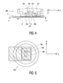
- Fig. 4 is a schematic, cross-sectional view of a distal end portion of a third example of an optical system for a device as shown in Fig. 1, of a layer to which the radiation is directed and of a liquid flow maintained in operation;
- Fig. 5 is a schematic, bottom view along the line V-V in Fig. 4; and
- Fig. 6 is a schematic top plan view representation of a wafer stepper/scanner for optical lithography.
- In the manufacture of an optically scannable information carrier, such as a CD or a DVD, a disc-
shaped substrate 3 of glass (see Fig. 1) carrying a thinphotosensitive layer 5 on one of its two sides is irradiated by means of amodulated radiation beam 7, for instance a DUV laser beam with a wavelength of approximately 260 nm. To irradiate thephotosensitive layer 5, use is made of an example 25 of a device in accordance with the invention, which device is described hereinafter with reference to Figs. 1-3. Theradiation beam 7 is focused to ascanning spot 11 on thephotosensitive layer 5 by an optical system, according to the present example in the form of alens system 9, including a plurality of optical elements in the form of lenses. Thelens system 9 includes an objective lens 55, which is secured in a lens holder 57. Thelens system 9 further includes a mostdistal lens 59, which is the one of the optical elements of thelens system 9 that is located nearest to thelayer 5 when in operation. Aninterspace 53 is maintained between thelayer 5 that is irradiated and the one of the optical elements of thelens system 9 that is located nearest to thelayer 5. The optical elements may also include other items than lenses, such as filters, shields, diffraction gratings or mirrors. - The
layer 5 and thelens system 9 are displaced with respect to each other, so that themodulated radiation beam 7 on thephotosensitive layer 5 successively irradiates a series of spaced apart irradiated portions of thelayer 5 and does not irradiate portions of thelayer 5 in-between the irradiated portions. The irradiatedphotosensitive layer 5 is subsequently developed by means of a developing liquid, which dissolves the irradiatedelements 13 and leaves thenon-irradiated elements 15 on thesubstrate 3. It is also possible to provide that the irradiated portions are left while the non-irradiated portions are dissolved. In both cases, a series of pits or bumps, which corresponds to the desired series of pit-shaped information elements on the information carrier, are formed in thephotosensitive layer 5. Thephotosensitive layer 5 is subsequently covered with a comparatively thin layer of for instance nickel by means of a sputtering process. Subsequently, this thin layer is covered with a comparatively thick nickel layer in an electro deposition process. In the nickel layer, which is eventually removed from thesubstrate 3, the pattern of pits formed in thephotosensitive layer 5 leaves a corresponding pattern that is a negative of the pattern to be formed in the information carrier to be manufactured, i.e. the master mold comprises a series of raised portions, which correspond to the series of pit-shaped elements formed in thephotosensitive layer 5 and to the desired series of pit-shaped information elements on the information carrier. The master mold is thus rendered suitable for use as a mold in an injection-molding machine for injection molding the desired information carriers. Generally, however, a copy of the master mold is used as the mold for injection molding instead of the master mold, which copy of the master mold is commonly referred to as daughter mold, which is manufactured by means of the master mold using a customary replica process which is known per se. - The
substrate 3 with thephotosensitive layer 5 is placed on a table 27 that is rotatable about an axis ofrotation 29, which extends perpendicularly to the table 27 and thesubstrate 3. The table can be driven by means of afirst electromotor 31. Thedevice 25 further comprises aradiation source 33, which, in the example shown, is a laser source, which is secured in a fixed position to aframe 35 of thedevice 25. It is observed that, as an alternative, the radiation may also be obtained from outside the device. Control over the radiation directed to thelayer 5 can be achieved in many ways, for instance by controlling theradiation source 33 and/or by controlling a shutter or radiation diverter (not shown) between theradiation source 33 and thelayer 5. - The
optical lens system 9 is secured onto afirst traveller 37, which can be displaced radially (parallel to the X-direction in the drawings) relative to the axis ofrotation 29, by means of afirst displacement structure 39. For this purpose, thefirst displacement structure 39 includes asecond electromotor 41 by means of which thefirst traveller 37 can be displaced over astraight guide 43, which extends parallel to the X-direction and is fixed relative to theframe 35. - A
mirror 45 in line with anoptical axis 49 of thelens system 9 is also secured to thefirst traveller 37. In operation, theradiation beam 7 generated by theradiation source 33 follows a radiation beam path 47 extending parallel to the X-direction, and theradiation beam 7 is deflected by themirror 45 in a direction parallel to theoptical axis 49 of thelens system 9. Thelens system 9 can be displaced in the direction of itsoptical axis 49 by means of afocus actuator 51, over comparatively small distances with respect to thefirst traveller 3, so that theradiation beam 7 can be focused on thephotosensitive layer 5. The table 27 with thesubstrate 5 is rotated about the axis ofrotation 29 at a comparatively high speed by means of thefirst motor 31, and thelens system 9 is displaced parallel to the X-direction by means of thesecond motor 41 at a comparatively low speed, so that thescanning spot 11 where theradiation beam 7 hits the layer follows a spiral-shaped track over thephotosensitive layer 5, leaving a trail of irradiated and non-irradiated elements extending in accordance with this spiral-shaped track. - The
device 25 can suitably be used to manufacture master molds having a comparatively high information density, i.e. by means of thedevice 25, a comparatively large number of irradiated elements can be provided per unit area of thephotosensitive layer 5. The attainable information density increases as thescanning spot 11 is smaller. The size of thescanning spot 11 is determined by the wavelength of theradiation beam 7 and by the numerical aperture of thelens system 9, the numerical aperture depending upon the optical refractive index of the medium present between thelens system 9 and thephotosensitive layer 5. Thescanning spot 11 is smaller as the refractive index of the medium present between thelens system 9 and thephotosensitive layer 5 is larger. Liquids typically have a much larger optical refractive index than air and therefore the portion of theinterspace 53 between thelens system 9 and thephotosensitive layer 5 through which thebeam 7 extends is maintained filled with a liquid - according to this example water. In the present example, water is also particularly suitable because it is transparent to theDUV radiation beam 7 used and it does not attack thephotosensitive layer 5. - As shown in Fig. 1, the
device 25 according to the present example further includes aliquid removal structure 77, which is provided with a pick-upmouth 79. The pick-upmouth 79 is secured onto asecond traveller 81 of thedevice 25, which can be displaced by means of asecond displacement structure 83 of thedevice 25 in a radial direction with respect to the axis ofrotation 29, according to the present example parallel to the X-direction, but another radial direction of displacement may be provided. For driving the displacement of thesecond traveller 81, thesecond displacement device 83 comprises athird electromotor 85 connected to thesecond traveller 81 for displacing the second traveller over astraight guide 87, which is attached to theframe 35 and extends in the directions of displacement of thesecond traveller 81. - In operation, the pick-up
mouth 79 is displaced by means of thethird motor 85. Thethird motor 85 is controlled so that thelens system 9 and the pick-upmouth 79 are continuously situated at substantially equal distances R from the axis ofrotation 29 of thesubstrate 3. In this manner, the pick-upmouth 79 is maintained in a position downstream from thelens system 9 where irradiated portions of thelayer 5 pass, so that the liquid supplied at the location of thelens system 9 is entrained by therotating layer 5 to the pick-upmouth 79 where the liquid is subsequently picked-up from thephotosensitive layer 5 by the pick-upmouth 79. As the water is thus removed from thephotosensitive layer 5 downstream from thelens system 9, it is substantially precluded that water that has already been used finds its way back to theinterspace 53, thereby disturbing the accurately dosed liquid flow in theinterspace 53. In operation, the pick-upmouth 79 is always at a distance R from the axis ofrotation 29 which corresponds to the distance R at which thelens system 9 is situated from the axis ofrotation 29, both the size and the capacity of the pick-upmouth 79 need only to be comparatively small to remove liquid that has already been used. - Figs. 2 and 3 show, in more detail, the
lens system 9, thesubstrate 3 with thephotosensitive layer 5, and theinterspace 53 between thephotosensitive layer 5 and thelens system 9. Thelens 59 nearest to thelayer 5 has anoptical surface 63 facing thesubstrate 3 and nearest to thesubstrate 3. Thelenses 55, 59 are suspended in ahousing 61, which includes aflat wall 65, which faces thelayer 5 and which substantially extends in an imaginary plane perpendicular to the optical axis of thelens 59 nearest to thelayer 5. In the surface of the lens system nearest to thelayer 5, arecess 92 facing thespot 11 to which theradiation 7 is directed is provided. Thesurface 63 of thelens 59 nearest to thelayer 5 forms an internal surface of therecess 92. Thissurface 63 also bounds the portion of theinterspace 53 through which theradiation 7 irradiates thespot 11. According to the present example, thesurface 63 of thelens 59 nearest to thelayer 5 is concave so that the deepest point of therecess 92 is in the middle, however, this surface may also be flat or convex. - In operation, the portion of the
interspace 53 through which theradiation 7 irradiates thespot 11 on thelayer 5 is maintained filled withliquid 91. In therecess 92, the liquid 91 is, at least to some extent, protected against being entrained from theinterspace 53. Since, the liquid 91 is less susceptible to being entrained away from the portion of theinterspace 53 through which the radiation passes to thespot 11, occurrence of the associated optical distortion caused by the portion of theinterspace 53 through which the radiation passes not being completely filled with liquid is thus counteracted. - Moreover, this allows the smallest size of the
interspace 53 measured parallel to the optical axis of thelenses 55, 59 to be relatively large. In turn, this reduces the risk of damage to thelens 59 nearest to thelayer 5 and the allowable tolerances on the tilt of the lens can be larger without increasing the risk of thelens 59 touching thelayer 5. - The
recess 92 may for instance be positioned and of such dimensions, so that only a portion of the radiation passes through the recess. However, for a particularly effective protection ofliquid 91 across the whole radiation beam, it is preferred that therecess 92 has a rim portion 93 closest to thelayer 5, which extends around theradiation 7 irradiating thespot 11. Accordingly, the portion of theinterspace 53 in therecess 92 in whichliquid 91 is shielded from being entrained extends throughout the whole cross-section of the radiation beam. - The optimum working distance between the
layer 5 and thewall 65, i.e. the portion of the lens assembly nearest to thelayer 5, is determined by two factors. On the one hand, the distance should be large enough to retain sufficient tolerance on the distance between thesubstrate 3 and arrangement of thelenses 55, 59 and thehousing 61. On the other hand, this distance should not be too large because this would require a too large liquid flow to maintain the immersed condition of the portion of theinterspace 53 through which the radiation passes to thespot 11. A presently preferred range for the smallest thickness of theinterspace 53 is 3-1500 µm and more preferably 3-500 µm if the liquid is water larger values for the smallest thickness of the interspace can be particularly advantageous if the liquid has a larger viscosity than water. Also the overall width of the outflow opening affects the upper end of the preferred range for the smallest thickness of the interspace, the smallest thickness of the interspace being preferably smaller than (100 + 1/20 * W)µm in which W is the overall width of the outflow opening measured in a plane parallel to thelayer 5. - The smallest thickness of the interspace may be larger than approximately 10 µm, for instance larger than 15 µm, 30 µm or even 100 µm, to increase the insensitivity to tolerances.
- To avoid inclusion of air bubbles in the liquid and for reliably maintaining the filled condition of the portion of the
interspace 53 through which theradiation 7 passes to thespot 11, liquid outflow is preferably such that a liquid volume between thewall 65 and thelayer 5 is maintained which includes a portion of theinterspace 53 upstream (in a direction opposite to the direction of relative movement of thelayer 5 in the area of the spot 11) of the portion of theinterspace 53 through which the radiation irradiates thespot 11. Thus, a safety margin of liquid upstream is formed which ensures that variations in the distance over which liquid is urged in upstream direction do not cause a disruption of the filled condition of the portion of theinterspace 53 through which theradiation 7 passes to thespot 11. - The most
downstream outflow opening 90 in thelens system 9 through which the liquid 91 is passed has a total projected cross-sectional passage area in a plane parallel to thelayer 5 of which, seen in a direction parallel to the optical axis of thelens system 109, the centre is located inside the portion of theinterspace 53 through which theradiation 7 irradiates thespot 11. Accordingly, the average path along which liquid flows out is at least to a large extent centred relative to the portion of theinterspace 53 through which radiation passes to thespot 11. Accordingly, the direction of movement of thelayer 5 and thelens arrangement 9 relative to each other in the area of thespot 11 can be varied substantially without disrupting complete immersion of the portion of theinterspace 53 through which thespot 11 is irradiated. Even if the direction of movement of thelayer 5 is varied substantially, the trace ofliquid 95 will still cover the entire portion of theinterspace 53 through which the spot is irradiated. Nevertheless, areas of theoutflow opening 90 around thebeam 7 are located close to the beam, so that superfluous wetting of thelayer 5 is limited. - According to the present example, the portion of the
interspace 53 through which theradiation 7 irradiates thespot 11 is also centrally located relative to theoutflow opening 90 to such an extent that thetrace 95 ofliquid 91 fed from theoutflow opening 90 into theinterspace 53 completely immerses the portion of theinterspace 53 through which theradiation 7 irradiates thespot 11, not only while, in the position of thespot 11, thelayer 5 and the at least onelens system 9 move relative to each other in the direction indicated by the arrow 52 (which indicates the direction of movement of thelayer 5 relative to the lens system 9), but also while, in the position of thespot 11, thelayer 5 andlens system 9 move relative to each other in opposite direction. - The more the direction of movement of the
layer 5 and thelens system 9 parallel to thelayer 5 in the area of thespot 11 can be changed without disrupting the immersion of theportion 194 of thearea 153 through which the radiation passes, the more the device is suitable for applications in which thespot 11 needs to move over the surface of the layer in widely varying directions, such as in imaging processes in which the spot is a two-dimensional image projected to thelayer 5. In such applications, the advantage of a comparatively large refractive index between the lens system and the medium between the lens system and the irradiated surface is that the image can be projected with a higher resolution, which in turn allows further miniaturization and/or an improved reliability. - An example of such applications is optical projection lithography for the processing of wafers for the manufacture of semiconductor devices. An apparatus and a method for this purpose are schematically illustrated in Fig. 6. Wafer steppers and wafer scanners are commercially available. Accordingly, such methods and apparatus are not described in great detail, but primarily to provide an understanding of liquid immersion as proposed in the present application in the context of such optical imaging applications.
- The projection lithography apparatus according to Fig. 6 includes a
wafer support 12 and aprojector 13 having alens assembly 14 above thewafer support 12. In Fig. 6, thewafer support 12 carries awafer 15 on which a plurality ofareas 16 are intended to be irradiated by a beam projecting an image or partial image of a mask orreticle 17 in ascanner 18 operatively connected to theprojector 13. The support table is moveable in X and Y direction alongspindles scanner 18 are connected to acontrol unit 23. - Usually one of two principles of operation are applied in optical lithography. In the so-called wafer stepper mode, the projector projects a complete image of the reticle onto one of the
areas 16 on thewafer 15. When the required exposure time has been reached, the light beam is switched off or obscured and thewafer 15 is moved by the spindle drives 21, 22 until anext area 16 of the wafer is in the required position in front of thelens assembly 14. Dependent on the relative positions of the exposed area and the next area to be exposed, this may involve relatively quick movement of thelens assembly 14 along the surface of the wafer in widely varying directions. The size of the irradiated spot on the surface of the wafer in which the image of the reticle is projected is typically about 20 x 20 mm, but larger and smaller spots are conceivable. - In particular when it is desired to manufacture larger semiconductor units, it is advantageous to project the image in the other mode, usually referred to as the wafer scanner mode. In that mode, only a slit-shaped portion of the reticle is projected as a slit shaped spot having a length that is several (for instance four or more times) times larger than its width in an
area 16 on the surface of thewafer 15. A typical size for the spot is for instance 30 x 5 mm). Then, thereticle 17 to be scanned is moved along the scanning window while thewafer support 12 is synchronously moved relative to thelens assembly 14 under control of thecontrol unit 23 with a velocity adapted so that only the projection spot, but not the scanned partial image portions of thereticle 17 that are projected on the wafer move relative to thewafer 15. Thus, the image of thereticle 17 is transferred to anarea 16 of the wafer as successive portions "unroll" as the spot progresses over the wafer. The movement of thewafer 15 relative to thelens assembly 14 while a running window portion of the reticle is projected onto thewafer 15 is usually carried out relatively slowly and usually each time in the same direction. After the complete image of areticle 17 has been projected onto thewafer 15, thewafer 15 is generally moved much more quickly relative to thelens assembly 14 to bring a next area of thewafer 15 where a next image of the or areticle 17 is to be projected in front of thelens assembly 14. This movement is carried out in widely varying directions dependent on the relative positions of the exposedarea 16 of thewafer 15 and thenext area 16 of thewafer 15 to be exposed. To be able to recommence irradiating the surface of thewafer 15 after the displacement of thewafer 15 relative to the lens 14 (i.e. also the lens or the lens and the wafer may be moved), it is advantageous if the liquid volume in the interspace between thelens 14 and the surface of thewafer 15 through which the radiation passes is immediately filled with liquid after completion of that movement, so that the space is reliably immersed before radiation is recommenced. - Also for optical lithography, water can be used, for instance if the radiation is light of a wavelength of 193 nm. However in some circumstances other liquids may be more suitable.
- Returning to Figs. 2 and 3, since the
recess 92 is bound by a concave portion of thesurface 63 of thelens 59 nearest to thespot 11 on thelayer 5 to which the beam of radiation7 is directed, the advantages of having arecess 92 are combined with a relatively uniform flow pattern throughout theportion 94 of theinterspace 53 through whichradiation 7 passes to thespot 11. In particular, a uniform pattern of flow velocity gradients in theinterspace 53 is obtained. In turn, the relatively uniform flow pattern is advantageous to avoid inducing vibrations and for obtaining a continuous uniform supply of fresh liquid and thereby a uniform, steady liquid temperature. These effects are both advantageous for avoiding optical disturbance of theradiation beam 7. - In Fig. 3, the dotted circle designated by
reference numeral 94 indicates the perimeter of the portion of theinterspace 53 between thelens 59 and thelayer 5 through which theradiation beam 7 passes. - For supplying
liquid 91 to theinterspace 53 between thelens 59 and thelayer 5, aliquid supply conduit 67 extends through thehousing 61 and leads to anoutflow opening 90. According to the present example, theoutflow opening 90 has the form of a canal structure in asurface 54, whichcanal structure 90 is open towards thelayer 5, for distributing supplied liquid 91 longitudinally along thecanal 90 and dispensing distributed liquid towards thelayer 5. In operation, the liquid 91 is distributed by thecanal structure 90 longitudinally along that canal structure and the liquid 91 is dispensed from thecanal structure 90 towards thelayer 5. This results in a relatively wideliquid trace 95 and full immersion of theportion 94 of theinterspace 53 through which theradiation beam 7 passes, even if the direction of movement of thelens system 9 and thelayer 5 relative to each other parallel to the plane of thelayer 5 is changed substantially. - The
canal 90 can have various forms. In the embodiment shown in Figs. 2 and 3, the canal is formed such that theoutflow opening 90 is located outside the radiation beam7 and extends around theportion 94 of theinterspace 53 through which theradiation 7 irradiates thespot 11. Thecross 96 indicates the centre, seen in a direction parallel to the optical axis of thelens system 9, of the total cross-sectional passage area of theoutflow opening 90. - The liquid 91 is preferably supplied at a pressure drop over the liquid between the
canal structure 90 and the environment that is just sufficient to keep portion of theinterspace 53 through which the radiation passes reliably immersed. Thus, the amount of water fed to the surface is kept to a minimum. - Furthermore, when the liquid 91 is dispensed via a canal shaped
outflow opening 90, the smallest thickness of the interspace 153 (in this example the distance between thelayer 5 and thesurface 54 of the wall portion 65) may be larger, without causing an undue risk of disrupting the immersion of theportion 94 of the interspace through which the radiation passes. Therefore, when the liquid is dispensed from a canal-shapedoutflow opening 90, thedisplacement structure lens system 9 are preferably positioned and dimensioned for maintaining the smallest thickness of theinterspace 53 in a range between 3 and 500 µm. - The flow rate with which the liquid 91 is supplied is preferably such that it can be reliably ensured that a laminar flow with an essentially linear velocity profile and preferably a homogeneous Couette flow is present in the
interspace 53. Such a flow exerts a substantially constant force on thewall 65 in which thecanal 90 is provided and on theside 63 of thelens 59 nearest to thelayer 5. As a result, the liquid present in theinterspace 53 exerts substantially no variable liquid forces on thelens system 9. Such varying liquid forces would lead to undesirable vibrations of thelens system 9 and hence to focusing errors and positioning errors of theradiation beam 7 on thephotosensitive layer 5. The flow is preferably free of air inclusions, so that theradiation beam 7 is not disturbed. - In Figs. 4 and 5 a second example of a
lens system 109 for devices such as the devices shown in Figs. 1 and 6 is shown. According to this example, theoutflow opening 190 downstream of theliquid supply canal 167 is also provided with a canal structure open towards the layer 5 (i.e. in the direction in which thebeam 107 is directed), but has a different, rectangular shape when seen in axial direction of thelens system 109. An essentially rectangular shape is particularly advantageous for reliably immersing arectangular area 194 of the interspace intersected by the radiation beam while maintaining a uniform liquid flow patter throughout the intersectedportion 194 of theinterspace 153, in particular if the movement of thelens system 109 and thelayer 5 relative to each other is in a direction perpendicular to one of the sides of therectangular canal structure 190. Such circumstances typically occur in optical projection lithography. - The
recess 192 is bounded by apassage 195 in a wall 165 perpendicular to the axis of thelens system 9 and a surface of thelens 159 nearest to thespot 11 and the surface of thelens 159 nearest to thespot 11 also bounds theportion 194 of theinterspace 153 through which theradiation 107 passes to thespot 11. Accordingly, thelens 159 is effectively protected against damage due to inadvertent contact between thelens system 109 and thelayer 5 on thesubstrate 3.
Claims (12)
- A method of irradiating a layer including:directing and focussing a radiation beam to a spot on said layer by means of at least one optical element;causing relative movement of the layer relative to said at least one optical element so that, successively, different portions of the layer are irradiated and an interspace between a surface of said at least one optical element nearest to said layer is maintained; andmaintaining at least a portion of said interspace through which said radiation irradiates said spot on said layer filled with a liquid, the liquid being supplied via a supply conduit and flowing out of an outflow opening;characterized in that at least one outflow opening via which the liquid flows out is provided in the form of at least one canal open towards said layer, said canal distributing supplied liquid longitudinally along said canal and dispensing distributed liquid towards said layer.
- A method according to claim 1, wherein the canal or canals are positioned such that, seen in a direction perpendicular to said layer, the canals define a total cross-sectional area having a centre in said portion of said interspace through which the radiation irradiates the spot.
- A method according to claim 1 or 2, wherein a smallest thickness of said interspace is maintained at 3-1500 µm.
- A method according to any one of the preceding claims, wherein at least a portion of said liquid fills up a recess through which said radiation irradiates said spot.
- A method according to claim 4, wherein the recess has a rim portion closest to said layer extending around said radiation irradiating said spot.
- A method according to claim 4 or 5, wherein said recess includes a concave portion of said surface of said at least one optical element nearest to said layer.
- A device for directing radiation to a layer including:at least one optical element for focussing a beam of radiation originating from said radiation source to a spot on said layer;a displacement structure for causing relative movement of the layer relative to said at least one optical element so that, successively, different portions of the layer are irradiated and an interspace between said layer and a surface of said at least one optical element nearest to said spot is maintained; andan outflow opening for supplying liquid to at least a portion of said interspace through which, in operation, said radiation irradiates said spot on said layer, said outflow opening having a total projected cross-sectional passage area in a plane perpendicular to an axis of said radiation beam;characterized in that the at least one outflow opening is formed by at least one canal open towards said layer, for distributing supplied liquid longitudinally along said canal and dispensing distributed liquid towards said layer.
- A device according to claim 7, wherein the outflow opening or a plurality of the outflow openings are positioned such that, seen in a direction parallel to said axis of said radiation beam, said total cross-sectional area has a centre in said portion of said gap through which the radiation irradiates the spot.
- A device according to claim 7 or 8, wherein said displacement structure and said recess are positioned and dimensioned for maintaining a smallest thickness of said interspace at 3-1500 µm.
- A device according to any one of the claims 7-9, wherein a recess is provided in a surface facing said spot, an internal surface of said recess bounding at least said portion of said interspace through which said radiation irradiates said spot.
- A device according to claim 10, wherein said recess has a rim portion closest to said layer extending around said portion of said interspace through which, in operation, said radiation irradiates said spot.
- A device according to claims 10 or 11, wherein said recess includes a concave portion of said surface of said at least one optical element nearest to said spot.
Priority Applications (1)
| Application Number | Priority Date | Filing Date | Title |
|---|---|---|---|
| EP06118252A EP1732075A3 (en) | 2002-12-19 | 2003-11-20 | Method and device for irradiating spots on a layer |
Applications Claiming Priority (3)
| Application Number | Priority Date | Filing Date | Title |
|---|---|---|---|
| EP02080376 | 2002-12-19 | ||
| EP06118252A EP1732075A3 (en) | 2002-12-19 | 2003-11-20 | Method and device for irradiating spots on a layer |
| EP03775698A EP1584089B1 (en) | 2002-12-19 | 2003-11-20 | Method and device for irradiating spots on a layer |
Related Parent Applications (2)
| Application Number | Title | Priority Date | Filing Date |
|---|---|---|---|
| EP03775698A Division EP1584089B1 (en) | 2002-12-19 | 2003-11-20 | Method and device for irradiating spots on a layer |
| EP03775698.8 Division | 2003-11-20 |
Publications (2)
| Publication Number | Publication Date |
|---|---|
| EP1732075A2 true EP1732075A2 (en) | 2006-12-13 |
| EP1732075A3 EP1732075A3 (en) | 2007-02-21 |
Family
ID=32668762
Family Applications (2)
| Application Number | Title | Priority Date | Filing Date |
|---|---|---|---|
| EP03775698A Expired - Lifetime EP1584089B1 (en) | 2002-12-19 | 2003-11-20 | Method and device for irradiating spots on a layer |
| EP06118252A Withdrawn EP1732075A3 (en) | 2002-12-19 | 2003-11-20 | Method and device for irradiating spots on a layer |
Family Applications Before (1)
| Application Number | Title | Priority Date | Filing Date |
|---|---|---|---|
| EP03775698A Expired - Lifetime EP1584089B1 (en) | 2002-12-19 | 2003-11-20 | Method and device for irradiating spots on a layer |
Country Status (11)
| Country | Link |
|---|---|
| US (1) | US7399978B2 (en) |
| EP (2) | EP1584089B1 (en) |
| JP (1) | JP4364806B2 (en) |
| KR (1) | KR100971441B1 (en) |
| CN (1) | CN100385535C (en) |
| AT (1) | ATE335272T1 (en) |
| AU (1) | AU2003283717A1 (en) |
| DE (1) | DE60307322T2 (en) |
| ES (1) | ES2268450T3 (en) |
| TW (1) | TWI288403B (en) |
| WO (1) | WO2004057590A1 (en) |
Cited By (1)
| Publication number | Priority date | Publication date | Assignee | Title |
|---|---|---|---|---|
| EP2017833A1 (en) * | 2007-07-16 | 2009-01-21 | Nederlandse Organisatie voor toegepast- natuurwetenschappelijk onderzoek TNO | Scanned writing of an exposure pattern on a substrate |
Families Citing this family (247)
| Publication number | Priority date | Publication date | Assignee | Title |
|---|---|---|---|---|
| US10503084B2 (en) | 2002-11-12 | 2019-12-10 | Asml Netherlands B.V. | Lithographic apparatus and device manufacturing method |
| DE60335595D1 (en) | 2002-11-12 | 2011-02-17 | Asml Netherlands Bv | Immersion lithographic apparatus and method of making a device |
| CN100568101C (en) | 2002-11-12 | 2009-12-09 | Asml荷兰有限公司 | Lithographic equipment and device making method |
| SG121822A1 (en) | 2002-11-12 | 2006-05-26 | Asml Netherlands Bv | Lithographic apparatus and device manufacturing method |
| US9482966B2 (en) | 2002-11-12 | 2016-11-01 | Asml Netherlands B.V. | Lithographic apparatus and device manufacturing method |
| KR100585476B1 (en) | 2002-11-12 | 2006-06-07 | 에이에스엠엘 네델란즈 비.브이. | Lithographic Apparatus and Device Manufacturing Method |
| CN101349876B (en) | 2002-11-12 | 2010-12-01 | Asml荷兰有限公司 | Immersion lithographic apparatus and device manufacturing method |
| US7110081B2 (en) | 2002-11-12 | 2006-09-19 | Asml Netherlands B.V. | Lithographic apparatus and device manufacturing method |
| SG131766A1 (en) | 2002-11-18 | 2007-05-28 | Asml Netherlands Bv | Lithographic apparatus and device manufacturing method |
| TWI255971B (en) | 2002-11-29 | 2006-06-01 | Asml Netherlands Bv | Lithographic apparatus and device manufacturing method |
| US7242455B2 (en) | 2002-12-10 | 2007-07-10 | Nikon Corporation | Exposure apparatus and method for producing device |
| WO2004053955A1 (en) | 2002-12-10 | 2004-06-24 | Nikon Corporation | Exposure system and device producing method |
| SG150388A1 (en) | 2002-12-10 | 2009-03-30 | Nikon Corp | Exposure apparatus and method for producing device |
| SG171468A1 (en) | 2002-12-10 | 2011-06-29 | Nikon Corp | Exposure apparatus and method for producing device |
| AU2003289271A1 (en) | 2002-12-10 | 2004-06-30 | Nikon Corporation | Exposure apparatus, exposure method and method for manufacturing device |
| JP4352874B2 (en) | 2002-12-10 | 2009-10-28 | 株式会社ニコン | Exposure apparatus and device manufacturing method |
| US7948604B2 (en) | 2002-12-10 | 2011-05-24 | Nikon Corporation | Exposure apparatus and method for producing device |
| DE10261775A1 (en) | 2002-12-20 | 2004-07-01 | Carl Zeiss Smt Ag | Device for the optical measurement of an imaging system |
| KR101381538B1 (en) | 2003-02-26 | 2014-04-04 | 가부시키가이샤 니콘 | Exposure apparatus and method, and method of manufacturing device |
| WO2004086470A1 (en) | 2003-03-25 | 2004-10-07 | Nikon Corporation | Exposure system and device production method |
| WO2004090956A1 (en) | 2003-04-07 | 2004-10-21 | Nikon Corporation | Exposure apparatus and method for manufacturing device |
| KR20110104084A (en) | 2003-04-09 | 2011-09-21 | 가부시키가이샤 니콘 | Immersion lithography fluid control system |
| KR101129213B1 (en) | 2003-04-10 | 2012-03-27 | 가부시키가이샤 니콘 | Run-off path to collect liquid for an immersion lithography apparatus |
| KR101431938B1 (en) | 2003-04-10 | 2014-08-19 | 가부시키가이샤 니콘 | Environmental system including a transport region for an immersion lithography apparatus |
| EP2950148B1 (en) | 2003-04-10 | 2016-09-21 | Nikon Corporation | Environmental system including vaccum scavenge for an immersion lithography apparatus |
| SG2013077797A (en) | 2003-04-11 | 2017-02-27 | Nippon Kogaku Kk | Cleanup method for optics in immersion lithography |
| SG139736A1 (en) | 2003-04-11 | 2008-02-29 | Nikon Corp | Apparatus having an immersion fluid system configured to maintain immersion fluid in a gap adjacent an optical assembly |
| WO2004092830A2 (en) | 2003-04-11 | 2004-10-28 | Nikon Corporation | Liquid jet and recovery system for immersion lithography |
| EP1614000B1 (en) | 2003-04-17 | 2012-01-18 | Nikon Corporation | Immersion lithographic apparatus |
| TWI295414B (en) | 2003-05-13 | 2008-04-01 | Asml Netherlands Bv | Lithographic apparatus and device manufacturing method |
| TWI503865B (en) | 2003-05-23 | 2015-10-11 | 尼康股份有限公司 | A method of manufacturing an exposure apparatus and an element |
| TWI463533B (en) | 2003-05-23 | 2014-12-01 | 尼康股份有限公司 | An exposure method, an exposure apparatus, and an element manufacturing method |
| KR20110110320A (en) | 2003-05-28 | 2011-10-06 | 가부시키가이샤 니콘 | Exposure method, exposure device, and device manufacturing method |
| TWI347741B (en) | 2003-05-30 | 2011-08-21 | Asml Netherlands Bv | Lithographic apparatus and device manufacturing method |
| US7213963B2 (en) | 2003-06-09 | 2007-05-08 | Asml Netherlands B.V. | Lithographic apparatus and device manufacturing method |
| EP1486827B1 (en) | 2003-06-11 | 2011-11-02 | ASML Netherlands B.V. | Lithographic apparatus and device manufacturing method |
| EP3104396B1 (en) | 2003-06-13 | 2018-03-21 | Nikon Corporation | Exposure method, substrate stage, exposure apparatus, and device manufacturing method |
| US6867844B2 (en) * | 2003-06-19 | 2005-03-15 | Asml Holding N.V. | Immersion photolithography system and method using microchannel nozzles |
| KR101265450B1 (en) | 2003-06-19 | 2013-05-16 | 가부시키가이샤 니콘 | Exposure device and device producing method |
| DE60308161T2 (en) | 2003-06-27 | 2007-08-09 | Asml Netherlands B.V. | Lithographic apparatus and method for making an article |
| EP1498778A1 (en) | 2003-06-27 | 2005-01-19 | ASML Netherlands B.V. | Lithographic apparatus and device manufacturing method |
| EP1494074A1 (en) | 2003-06-30 | 2005-01-05 | ASML Netherlands B.V. | Lithographic apparatus and device manufacturing method |
| DE60321779D1 (en) | 2003-06-30 | 2008-08-07 | Asml Netherlands Bv | Lithographic apparatus and method for making an article |
| JP4697138B2 (en) | 2003-07-08 | 2011-06-08 | 株式会社ニコン | Immersion lithography apparatus, immersion lithography method, and device manufacturing method |
| CN102944981A (en) | 2003-07-09 | 2013-02-27 | 株式会社尼康 | Exposure apparatus, and device fabricating method |
| EP2264531B1 (en) | 2003-07-09 | 2013-01-16 | Nikon Corporation | Exposure apparatus and device manufacturing method |
| KR101296501B1 (en) | 2003-07-09 | 2013-08-13 | 가부시키가이샤 니콘 | Exposure apparatus and method for manufacturing device |
| US7738074B2 (en) | 2003-07-16 | 2010-06-15 | Asml Netherlands B.V. | Lithographic apparatus and device manufacturing method |
| EP1500982A1 (en) | 2003-07-24 | 2005-01-26 | ASML Netherlands B.V. | Lithographic apparatus and device manufacturing method |
| JP4524669B2 (en) | 2003-07-25 | 2010-08-18 | 株式会社ニコン | Projection optical system inspection method and inspection apparatus |
| CN102323724B (en) | 2003-07-28 | 2014-08-13 | 株式会社尼康 | Liquid immersion exposure apparatus, producing method thereof, exposure apparatus and device producing method |
| EP1503244A1 (en) | 2003-07-28 | 2005-02-02 | ASML Netherlands B.V. | Lithographic projection apparatus and device manufacturing method |
| US7175968B2 (en) | 2003-07-28 | 2007-02-13 | Asml Netherlands B.V. | Lithographic apparatus, device manufacturing method and a substrate |
| US7779781B2 (en) | 2003-07-31 | 2010-08-24 | Asml Netherlands B.V. | Lithographic apparatus and device manufacturing method |
| EP2284615B1 (en) | 2003-08-26 | 2013-01-16 | Nikon Corporation | Exposure apparatus |
| US8149381B2 (en) | 2003-08-26 | 2012-04-03 | Nikon Corporation | Optical element and exposure apparatus |
| TWI245163B (en) | 2003-08-29 | 2005-12-11 | Asml Netherlands Bv | Lithographic apparatus and device manufacturing method |
| EP2261740B1 (en) | 2003-08-29 | 2014-07-09 | ASML Netherlands BV | Lithographic apparatus |
| CN101303536B (en) | 2003-08-29 | 2011-02-09 | 株式会社尼康 | Exposure apparatus and device producing method |
| TWI263859B (en) | 2003-08-29 | 2006-10-11 | Asml Netherlands Bv | Lithographic apparatus and device manufacturing method |
| US6954256B2 (en) | 2003-08-29 | 2005-10-11 | Asml Netherlands B.V. | Gradient immersion lithography |
| CN101430508B (en) | 2003-09-03 | 2011-08-10 | 株式会社尼康 | Device and method for supplying fluid for immersion lithography |
| WO2005029559A1 (en) | 2003-09-19 | 2005-03-31 | Nikon Corporation | Exposure apparatus and device producing method |
| KR101335736B1 (en) | 2003-09-29 | 2013-12-02 | 가부시키가이샤 니콘 | Exposure apparatus, exposure method, and device manufacturing method |
| DE60302897T2 (en) | 2003-09-29 | 2006-08-03 | Asml Netherlands B.V. | Lithographic apparatus and method of making a device |
| EP1519230A1 (en) | 2003-09-29 | 2005-03-30 | ASML Netherlands B.V. | Lithographic apparatus and device manufacturing method |
| US7158211B2 (en) | 2003-09-29 | 2007-01-02 | Asml Netherlands B.V. | Lithographic apparatus and device manufacturing method |
| JP4335213B2 (en) | 2003-10-08 | 2009-09-30 | 株式会社蔵王ニコン | Substrate transport apparatus, exposure apparatus, and device manufacturing method |
| KR101361892B1 (en) | 2003-10-08 | 2014-02-12 | 가부시키가이샤 자오 니콘 | Substrate carrying apparatus, substrate carrying method, exposure apparatus, exposure method, and method for producing device |
| TWI553701B (en) | 2003-10-09 | 2016-10-11 | 尼康股份有限公司 | Exposure apparatus and exposure method, component manufacturing method |
| EP1524558A1 (en) | 2003-10-15 | 2005-04-20 | ASML Netherlands B.V. | Lithographic apparatus and device manufacturing method |
| EP1524557A1 (en) | 2003-10-15 | 2005-04-20 | ASML Netherlands B.V. | Lithographic apparatus and device manufacturing method |
| EP1679738A4 (en) | 2003-10-28 | 2008-08-06 | Nikon Corp | Exposure apparatus, exposure method, and device producing method |
| US7352433B2 (en) | 2003-10-28 | 2008-04-01 | Asml Netherlands B.V. | Lithographic apparatus and device manufacturing method |
| US7411653B2 (en) | 2003-10-28 | 2008-08-12 | Asml Netherlands B.V. | Lithographic apparatus |
| US7528929B2 (en) | 2003-11-14 | 2009-05-05 | Asml Netherlands B.V. | Lithographic apparatus and device manufacturing method |
| US7545481B2 (en) | 2003-11-24 | 2009-06-09 | Asml Netherlands B.V. | Lithographic apparatus and device manufacturing method |
| EP3139214B1 (en) | 2003-12-03 | 2019-01-30 | Nikon Corporation | Exposure apparatus, exposure method, and device manufacturing method |
| KR101281397B1 (en) | 2003-12-15 | 2013-07-02 | 가부시키가이샤 니콘 | Stage system, exposure apparatus and exposure method |
| US7589818B2 (en) | 2003-12-23 | 2009-09-15 | Asml Netherlands B.V. | Lithographic apparatus, alignment apparatus, device manufacturing method, and a method of converting an apparatus |
| US7394521B2 (en) | 2003-12-23 | 2008-07-01 | Asml Netherlands B.V. | Lithographic apparatus and device manufacturing method |
| EP1706793B1 (en) | 2004-01-20 | 2010-03-03 | Carl Zeiss SMT AG | Exposure apparatus and measuring device for a projection lens |
| US7589822B2 (en) | 2004-02-02 | 2009-09-15 | Nikon Corporation | Stage drive method and stage unit, exposure apparatus, and device manufacturing method |
| KR101276392B1 (en) | 2004-02-03 | 2013-06-19 | 가부시키가이샤 니콘 | Exposure apparatus and method of producing device |
| EP3267469B1 (en) | 2004-02-04 | 2018-08-15 | Nikon Corporation | Exposure apparatus, exposure method, and method for producing device |
| US7050146B2 (en) | 2004-02-09 | 2006-05-23 | Asml Netherlands B.V. | Lithographic apparatus and device manufacturing method |
| JP2007522508A (en) * | 2004-02-13 | 2007-08-09 | カール・ツアイス・エスエムテイ・アーゲー | Projection objective for a microlithographic projection exposure apparatus |
| DE102004013886A1 (en) | 2004-03-16 | 2005-10-06 | Carl Zeiss Smt Ag | Multiple Exposure Method, Microlithography Projection Exposure System and Projection System |
| TWI628697B (en) | 2004-03-25 | 2018-07-01 | 尼康股份有限公司 | Exposure apparatus, and device manufacturing method |
| US7034917B2 (en) | 2004-04-01 | 2006-04-25 | Asml Netherlands B.V. | Lithographic apparatus, device manufacturing method and device manufactured thereby |
| US7227619B2 (en) | 2004-04-01 | 2007-06-05 | Asml Netherlands B.V. | Lithographic apparatus and device manufacturing method |
| US7295283B2 (en) | 2004-04-02 | 2007-11-13 | Asml Netherlands B.V. | Lithographic apparatus and device manufacturing method |
| US7898642B2 (en) | 2004-04-14 | 2011-03-01 | Asml Netherlands B.V. | Lithographic apparatus and device manufacturing method |
| KR101330370B1 (en) | 2004-04-19 | 2013-11-15 | 가부시키가이샤 니콘 | Exposure apparatus and device producing method |
| US7379159B2 (en) | 2004-05-03 | 2008-05-27 | Asml Netherlands B.V. | Lithographic apparatus and device manufacturing method |
| WO2005111722A2 (en) | 2004-05-04 | 2005-11-24 | Nikon Corporation | Apparatus and method for providing fluid for immersion lithography |
| US7616383B2 (en) | 2004-05-18 | 2009-11-10 | Asml Netherlands B.V. | Lithographic apparatus and device manufacturing method |
| US7486381B2 (en) | 2004-05-21 | 2009-02-03 | Asml Netherlands B.V. | Lithographic apparatus and device manufacturing method |
| KR101257960B1 (en) | 2004-06-04 | 2013-04-24 | 칼 짜이스 에스엠테 게엠베하 | System for measuring the image quality of an optical imaging system |
| KR101433496B1 (en) | 2004-06-09 | 2014-08-22 | 가부시키가이샤 니콘 | Exposure system and device production method |
| US8508713B2 (en) | 2004-06-10 | 2013-08-13 | Nikon Corporation | Exposure apparatus, exposure method, and method for producing device |
| US8482716B2 (en) | 2004-06-10 | 2013-07-09 | Nikon Corporation | Exposure apparatus, exposure method, and method for producing device |
| CN101685269B (en) | 2004-06-10 | 2011-09-14 | 尼康股份有限公司 | Exposure apparatus and device producing method |
| US8373843B2 (en) | 2004-06-10 | 2013-02-12 | Nikon Corporation | Exposure apparatus, exposure method, and method for producing device |
| US8717533B2 (en) | 2004-06-10 | 2014-05-06 | Nikon Corporation | Exposure apparatus, exposure method, and method for producing device |
| US7481867B2 (en) | 2004-06-16 | 2009-01-27 | Edwards Limited | Vacuum system for immersion photolithography |
| US7463330B2 (en) | 2004-07-07 | 2008-12-09 | Asml Netherlands B.V. | Lithographic apparatus and device manufacturing method |
| KR101202230B1 (en) | 2004-07-12 | 2012-11-16 | 가부시키가이샤 니콘 | Exposure equipment and device manufacturing method |
| US7161663B2 (en) | 2004-07-22 | 2007-01-09 | Asml Netherlands B.V. | Lithographic apparatus |
| US7304715B2 (en) | 2004-08-13 | 2007-12-04 | Asml Netherlands B.V. | Lithographic apparatus and device manufacturing method |
| WO2006019124A1 (en) | 2004-08-18 | 2006-02-23 | Nikon Corporation | Exposure apparatus and device manufacturing method |
| US7701550B2 (en) | 2004-08-19 | 2010-04-20 | Asml Netherlands B.V. | Lithographic apparatus and device manufacturing method |
| KR101506100B1 (en) | 2004-09-17 | 2015-03-26 | 가부시키가이샤 니콘 | Exposure apparatus, exposure method, and method for manufacturing device |
| US7133114B2 (en) | 2004-09-20 | 2006-11-07 | Asml Netherlands B.V. | Lithographic apparatus and device manufacturing method |
| US7522261B2 (en) | 2004-09-24 | 2009-04-21 | Asml Netherlands B.V. | Lithographic apparatus and device manufacturing method |
| US7355674B2 (en) | 2004-09-28 | 2008-04-08 | Asml Netherlands B.V. | Lithographic apparatus, device manufacturing method and computer program product |
| US7894040B2 (en) | 2004-10-05 | 2011-02-22 | Asml Netherlands B.V. | Lithographic apparatus and device manufacturing method |
| US7209213B2 (en) | 2004-10-07 | 2007-04-24 | Asml Netherlands B.V. | Lithographic apparatus and device manufacturing method |
| CN100477083C (en) | 2004-10-13 | 2009-04-08 | 株式会社尼康 | Exposing device, exposing method, and assembly manufacturing method |
| US7119876B2 (en) | 2004-10-18 | 2006-10-10 | Asml Netherlands B.V. | Lithographic apparatus and device manufacturing method |
| US7379155B2 (en) | 2004-10-18 | 2008-05-27 | Asml Netherlands B.V. | Lithographic apparatus and device manufacturing method |
| KR101236120B1 (en) | 2004-10-26 | 2013-02-28 | 가부시키가이샤 니콘 | Substrate processing method, exposure apparatus and method for manufacturing device |
| US7583357B2 (en) | 2004-11-12 | 2009-09-01 | Asml Netherlands B.V. | Lithographic apparatus and device manufacturing method |
| US7414699B2 (en) | 2004-11-12 | 2008-08-19 | Asml Netherlands B.V. | Lithographic apparatus and device manufacturing method |
| US7251013B2 (en) | 2004-11-12 | 2007-07-31 | Asml Netherlands B.V. | Lithographic apparatus and device manufacturing method |
| US7423720B2 (en) * | 2004-11-12 | 2008-09-09 | Asml Netherlands B.V. | Lithographic apparatus and device manufacturing method |
| US7411657B2 (en) | 2004-11-17 | 2008-08-12 | Asml Netherlands B.V. | Lithographic apparatus and device manufacturing method |
| US7145630B2 (en) | 2004-11-23 | 2006-12-05 | Asml Netherlands B.V. | Lithographic apparatus and device manufacturing method |
| US7161654B2 (en) | 2004-12-02 | 2007-01-09 | Asml Netherlands B.V. | Lithographic apparatus and device manufacturing method |
| US7446850B2 (en) | 2004-12-03 | 2008-11-04 | Asml Netherlands B.V. | Lithographic apparatus and device manufacturing method |
| US7196770B2 (en) | 2004-12-07 | 2007-03-27 | Asml Netherlands B.V. | Prewetting of substrate before immersion exposure |
| US7248334B2 (en) | 2004-12-07 | 2007-07-24 | Asml Netherlands B.V. | Sensor shield |
| US7397533B2 (en) | 2004-12-07 | 2008-07-08 | Asml Netherlands B.V. | Lithographic apparatus and device manufacturing method |
| US7365827B2 (en) | 2004-12-08 | 2008-04-29 | Asml Netherlands B.V. | Lithographic apparatus and device manufacturing method |
| JP4752473B2 (en) | 2004-12-09 | 2011-08-17 | 株式会社ニコン | Exposure apparatus, exposure method, and device manufacturing method |
| US7352440B2 (en) | 2004-12-10 | 2008-04-01 | Asml Netherlands B.V. | Substrate placement in immersion lithography |
| US7403261B2 (en) | 2004-12-15 | 2008-07-22 | Asml Netherlands B.V. | Lithographic apparatus and device manufacturing method |
| US7880860B2 (en) | 2004-12-20 | 2011-02-01 | Asml Netherlands B.V. | Lithographic apparatus and device manufacturing method |
| US7528931B2 (en) | 2004-12-20 | 2009-05-05 | Asml Netherlands B.V. | Lithographic apparatus and device manufacturing method |
| US7405805B2 (en) | 2004-12-28 | 2008-07-29 | Asml Netherlands B.V. | Lithographic apparatus and device manufacturing method |
| US7491661B2 (en) | 2004-12-28 | 2009-02-17 | Asml Netherlands B.V. | Device manufacturing method, top coat material and substrate |
| US20060147821A1 (en) | 2004-12-30 | 2006-07-06 | Asml Netherlands B.V. | Lithographic apparatus and device manufacturing method |
| SG124351A1 (en) | 2005-01-14 | 2006-08-30 | Asml Netherlands Bv | Lithographic apparatus and device manufacturing method |
| SG124359A1 (en) | 2005-01-14 | 2006-08-30 | Asml Netherlands Bv | Lithographic apparatus and device manufacturing method |
| US8692973B2 (en) | 2005-01-31 | 2014-04-08 | Nikon Corporation | Exposure apparatus and method for producing device |
| WO2006080516A1 (en) | 2005-01-31 | 2006-08-03 | Nikon Corporation | Exposure apparatus and method for manufacturing device |
| KR101140755B1 (en) | 2005-02-10 | 2012-05-03 | 에이에스엠엘 네델란즈 비.브이. | Immersion liquid, exposure apparatus, and exposure process |
| US8018573B2 (en) | 2005-02-22 | 2011-09-13 | Asml Netherlands B.V. | Lithographic apparatus and device manufacturing method |
| US7224431B2 (en) | 2005-02-22 | 2007-05-29 | Asml Netherlands B.V. | Lithographic apparatus and device manufacturing method |
| US7378025B2 (en) | 2005-02-22 | 2008-05-27 | Asml Netherlands B.V. | Fluid filtration method, fluid filtered thereby, lithographic apparatus and device manufacturing method |
| US7428038B2 (en) | 2005-02-28 | 2008-09-23 | Asml Netherlands B.V. | Lithographic apparatus, device manufacturing method and apparatus for de-gassing a liquid |
| US7282701B2 (en) | 2005-02-28 | 2007-10-16 | Asml Netherlands B.V. | Sensor for use in a lithographic apparatus |
| US7324185B2 (en) | 2005-03-04 | 2008-01-29 | Asml Netherlands B.V. | Lithographic apparatus and device manufacturing method |
| US7684010B2 (en) | 2005-03-09 | 2010-03-23 | Asml Netherlands B.V. | Lithographic apparatus, device manufacturing method, seal structure, method of removing an object and a method of sealing |
| JP4844186B2 (en) | 2005-03-18 | 2011-12-28 | 株式会社ニコン | Plate member, substrate holding apparatus, exposure apparatus and exposure method, and device manufacturing method |
| WO2006101024A1 (en) | 2005-03-18 | 2006-09-28 | Nikon Corporation | Exposure method, exposure apparatus, device manufacturing method and exposure apparatus evaluating method |
| US7330238B2 (en) | 2005-03-28 | 2008-02-12 | Asml Netherlands, B.V. | Lithographic apparatus, immersion projection apparatus and device manufacturing method |
| WO2006106832A1 (en) | 2005-03-30 | 2006-10-12 | Nikon Corporation | Method for determining exposure conditions, exposure method, exposure device, and apparatus for producing device |
| US7411654B2 (en) | 2005-04-05 | 2008-08-12 | Asml Netherlands B.V. | Lithographic apparatus and device manufacturing method |
| US7291850B2 (en) | 2005-04-08 | 2007-11-06 | Asml Netherlands B.V. | Lithographic apparatus and device manufacturing method |
| USRE43576E1 (en) | 2005-04-08 | 2012-08-14 | Asml Netherlands B.V. | Dual stage lithographic apparatus and device manufacturing method |
| EP1873816A4 (en) | 2005-04-18 | 2010-11-24 | Nikon Corp | Exposure device, exposure method, and device manufacturing method |
| KR20070122445A (en) | 2005-04-28 | 2007-12-31 | 가부시키가이샤 니콘 | Exposure method, exposure apparatus and device manufacturing method |
| US8248577B2 (en) | 2005-05-03 | 2012-08-21 | Asml Netherlands B.V. | Lithographic apparatus and device manufacturing method |
| US7317507B2 (en) | 2005-05-03 | 2008-01-08 | Asml Netherlands B.V. | Lithographic apparatus and device manufacturing method |
| US7433016B2 (en) | 2005-05-03 | 2008-10-07 | Asml Netherlands B.V. | Lithographic apparatus and device manufacturing method |
| US7751027B2 (en) | 2005-06-21 | 2010-07-06 | Asml Netherlands B.V. | Lithographic apparatus and device manufacturing method |
| US7652746B2 (en) | 2005-06-21 | 2010-01-26 | Asml Netherlands B.V. | Lithographic apparatus and device manufacturing method |
| US7834974B2 (en) | 2005-06-28 | 2010-11-16 | Asml Netherlands B.V. | Lithographic apparatus and device manufacturing method |
| US7468779B2 (en) | 2005-06-28 | 2008-12-23 | Asml Netherlands B.V. | Lithographic apparatus and device manufacturing method |
| US7474379B2 (en) | 2005-06-28 | 2009-01-06 | Asml Netherlands B.V. | Lithographic apparatus and device manufacturing method |
| US8179517B2 (en) | 2005-06-30 | 2012-05-15 | Nikon Corporation | Exposure apparatus and method, maintenance method for exposure apparatus, and device manufacturing method |
| US7535644B2 (en) | 2005-08-12 | 2009-05-19 | Asml Netherlands B.V. | Lens element, lithographic apparatus, device manufacturing method, and device manufactured thereby |
| US8054445B2 (en) | 2005-08-16 | 2011-11-08 | Asml Netherlands B.V. | Lithographic apparatus and device manufacturing method |
| WO2007023813A1 (en) | 2005-08-23 | 2007-03-01 | Nikon Corporation | Exposure apparatus, exposure method, and device manufacturing method |
| JPWO2007034838A1 (en) * | 2005-09-21 | 2009-03-26 | 株式会社ニコン | Exposure apparatus, exposure method, and device manufacturing method |
| US7411658B2 (en) | 2005-10-06 | 2008-08-12 | Asml Netherlands B.V. | Lithographic apparatus and device manufacturing method |
| WO2007055199A1 (en) | 2005-11-09 | 2007-05-18 | Nikon Corporation | Exposure apparatus and method, and method for manufacturing device |
| US7804577B2 (en) | 2005-11-16 | 2010-09-28 | Asml Netherlands B.V. | Lithographic apparatus |
| US7864292B2 (en) | 2005-11-16 | 2011-01-04 | Asml Netherlands B.V. | Lithographic apparatus and device manufacturing method |
| US7656501B2 (en) | 2005-11-16 | 2010-02-02 | Asml Netherlands B.V. | Lithographic apparatus |
| US7803516B2 (en) | 2005-11-21 | 2010-09-28 | Nikon Corporation | Exposure method, device manufacturing method using the same, exposure apparatus, and substrate processing method and apparatus |
| JP2007165869A (en) | 2005-11-21 | 2007-06-28 | Nikon Corp | Exposure method and method for manufacturing device using same, exposure device, and method and device of processing substrate |
| US7633073B2 (en) | 2005-11-23 | 2009-12-15 | Asml Netherlands B.V. | Lithographic apparatus and device manufacturing method |
| US7782442B2 (en) | 2005-12-06 | 2010-08-24 | Nikon Corporation | Exposure apparatus, exposure method, projection optical system and device producing method |
| TW200722935A (en) | 2005-12-06 | 2007-06-16 | Nikon Corp | Exposure apparatus, exposure method, projection optical system and device manufacturing method |
| JP5194799B2 (en) | 2005-12-06 | 2013-05-08 | 株式会社ニコン | Exposure method, exposure apparatus, and device manufacturing method |
| US7420194B2 (en) | 2005-12-27 | 2008-09-02 | Asml Netherlands B.V. | Lithographic apparatus and substrate edge seal |
| US8411271B2 (en) | 2005-12-28 | 2013-04-02 | Nikon Corporation | Pattern forming method, pattern forming apparatus, and device manufacturing method |
| CN101300662B (en) | 2005-12-28 | 2012-05-09 | 株式会社尼康 | Pattern forming method, pattern forming apparatus, and device manufacturing method |
| US8953148B2 (en) | 2005-12-28 | 2015-02-10 | Nikon Corporation | Exposure apparatus and making method thereof |
| CN102636966B (en) | 2005-12-28 | 2014-12-03 | 株式会社尼康 | Exposure method and exposure apparatus, and device manufacturing method |
| US7839483B2 (en) | 2005-12-28 | 2010-11-23 | Asml Netherlands B.V. | Lithographic apparatus, device manufacturing method and a control system |
| EP1978546A4 (en) | 2005-12-28 | 2010-08-04 | Nikon Corp | Exposure apparatus, exposure method, and device production method |
| US7649611B2 (en) | 2005-12-30 | 2010-01-19 | Asml Netherlands B.V. | Lithographic apparatus and device manufacturing method |
| WO2007083758A1 (en) | 2006-01-19 | 2007-07-26 | Nikon Corporation | Moving body drive method, moving body drive system, pattern formation method, pattern formation device, exposure method, exposure device, and device fabrication method |
| KR20080102192A (en) | 2006-02-16 | 2008-11-24 | 가부시키가이샤 니콘 | Exposure apparatus, exposing method, and device manufacturing method |
| WO2007094431A1 (en) | 2006-02-16 | 2007-08-23 | Nikon Corporation | Exposure apparatus, exposing method, and device manufacturing method |
| WO2007094470A1 (en) | 2006-02-16 | 2007-08-23 | Nikon Corporation | Exposure apparatus, exposure method and method for manufacturing device |
| EP1986222A4 (en) | 2006-02-16 | 2010-09-01 | Nikon Corp | Exposure apparatus, exposing method, and device manufacturing method |
| JP5195417B2 (en) | 2006-02-21 | 2013-05-08 | 株式会社ニコン | Pattern forming apparatus, exposure apparatus, exposure method, and device manufacturing method |
| JP5115859B2 (en) | 2006-02-21 | 2013-01-09 | 株式会社ニコン | Pattern forming apparatus, exposure apparatus, exposure method, and device manufacturing method |
| EP2003681B1 (en) | 2006-02-21 | 2014-11-12 | Nikon Corporation | Measuring apparatus, measuring method, pattern forming apparatus, pattern forming method, and device manufacturing method |
| JP5077770B2 (en) | 2006-03-07 | 2012-11-21 | 株式会社ニコン | Device manufacturing method, device manufacturing system, and measurement / inspection apparatus |
| WO2007105645A1 (en) | 2006-03-13 | 2007-09-20 | Nikon Corporation | Exposure apparatus, maintenance method, exposure method and device manufacturing method |
| US8045134B2 (en) | 2006-03-13 | 2011-10-25 | Asml Netherlands B.V. | Lithographic apparatus, control system and device manufacturing method |
| US9477158B2 (en) | 2006-04-14 | 2016-10-25 | Asml Netherlands B.V. | Lithographic apparatus and device manufacturing method |
| DE102006021797A1 (en) | 2006-05-09 | 2007-11-15 | Carl Zeiss Smt Ag | Optical imaging device with thermal damping |
| EP2037486A4 (en) | 2006-05-18 | 2012-01-11 | Nikon Corp | Exposure method and apparatus, maintenance method and device manufacturing method |
| US7969548B2 (en) | 2006-05-22 | 2011-06-28 | Asml Netherlands B.V. | Lithographic apparatus and lithographic apparatus cleaning method |
| JP2008004928A (en) | 2006-05-22 | 2008-01-10 | Nikon Corp | Exposure method and apparatus, maintenance method, and device manufacturing method |
| CN102156389A (en) | 2006-05-23 | 2011-08-17 | 株式会社尼康 | Maintenance method, exposure method and apparatus, and device manufacturing method |
| WO2007138834A1 (en) | 2006-05-31 | 2007-12-06 | Nikon Corporation | Exposure apparatus and exposure method |
| JP5245825B2 (en) | 2006-06-30 | 2013-07-24 | 株式会社ニコン | Maintenance method, exposure method and apparatus, and device manufacturing method |
| US8045135B2 (en) | 2006-11-22 | 2011-10-25 | Asml Netherlands B.V. | Lithographic apparatus with a fluid combining unit and related device manufacturing method |
| US8634053B2 (en) | 2006-12-07 | 2014-01-21 | Asml Netherlands B.V. | Lithographic apparatus and device manufacturing method |
| US9632425B2 (en) | 2006-12-07 | 2017-04-25 | Asml Holding N.V. | Lithographic apparatus, a dryer and a method of removing liquid from a surface |
| US7791709B2 (en) | 2006-12-08 | 2010-09-07 | Asml Netherlands B.V. | Substrate support and lithographic process |
| US8237911B2 (en) | 2007-03-15 | 2012-08-07 | Nikon Corporation | Apparatus and methods for keeping immersion fluid adjacent to an optical assembly during wafer exchange in an immersion lithography machine |
| JPWO2008132799A1 (en) | 2007-04-12 | 2010-07-22 | 株式会社ニコン | Measuring method, exposure method, and device manufacturing method |
| US7866330B2 (en) | 2007-05-04 | 2011-01-11 | Asml Netherlands B.V. | Cleaning device, a lithographic apparatus and a lithographic apparatus cleaning method |
| US8947629B2 (en) | 2007-05-04 | 2015-02-03 | Asml Netherlands B.V. | Cleaning device, a lithographic apparatus and a lithographic apparatus cleaning method |
| US7900641B2 (en) | 2007-05-04 | 2011-03-08 | Asml Netherlands B.V. | Cleaning device and a lithographic apparatus cleaning method |
| KR20100031694A (en) | 2007-05-28 | 2010-03-24 | 가부시키가이샤 니콘 | Exposure apparatus, device manufacturing method, cleaning device, cleaning method and exposure method |
| US8164736B2 (en) | 2007-05-29 | 2012-04-24 | Nikon Corporation | Exposure method, exposure apparatus, and method for producing device |
| US8098362B2 (en) | 2007-05-30 | 2012-01-17 | Nikon Corporation | Detection device, movable body apparatus, pattern formation apparatus and pattern formation method, exposure apparatus and exposure method, and device manufacturing method |
| US8547527B2 (en) | 2007-07-24 | 2013-10-01 | Nikon Corporation | Movable body drive method and movable body drive system, pattern formation method and pattern formation apparatus, and device manufacturing method |
| JP5177449B2 (en) | 2007-07-24 | 2013-04-03 | 株式会社ニコン | Moving body driving method and moving body driving system, pattern forming method and apparatus, exposure method and apparatus, and device manufacturing method |
| US8194232B2 (en) | 2007-07-24 | 2012-06-05 | Nikon Corporation | Movable body drive method and movable body drive system, pattern formation method and apparatus, exposure method and apparatus, position control method and position control system, and device manufacturing method |
| US8867022B2 (en) | 2007-08-24 | 2014-10-21 | Nikon Corporation | Movable body drive method and movable body drive system, pattern formation method and apparatus, and device manufacturing method |
| US8023106B2 (en) | 2007-08-24 | 2011-09-20 | Nikon Corporation | Movable body drive method and movable body drive system, pattern formation method and apparatus, exposure method and apparatus, and device manufacturing method |
| US9304412B2 (en) | 2007-08-24 | 2016-04-05 | Nikon Corporation | Movable body drive method and movable body drive system, pattern formation method and apparatus, exposure method and apparatus, device manufacturing method, and measuring method |
| US8237919B2 (en) | 2007-08-24 | 2012-08-07 | Nikon Corporation | Movable body drive method and movable body drive system, pattern formation method and apparatus, exposure method and apparatus, and device manufacturing method for continuous position measurement of movable body before and after switching between sensor heads |
| US8218129B2 (en) | 2007-08-24 | 2012-07-10 | Nikon Corporation | Movable body drive method and movable body drive system, pattern formation method and apparatus, exposure method and apparatus, device manufacturing method, measuring method, and position measurement system |
| NL1036186A1 (en) * | 2007-12-03 | 2009-06-04 | Asml Netherlands Bv | Lithographic apparatus and device manufacturing method. |
| TWI602033B (en) | 2007-12-28 | 2017-10-11 | Nippon Kogaku Kk | Exposure apparatus, moving body driving system, pattern forming apparatus, exposure method, and device manufacturing method |
| JP5097166B2 (en) | 2008-05-28 | 2012-12-12 | エーエスエムエル ネザーランズ ビー.ブイ. | Lithographic apparatus and method of operating the apparatus |
| US8384875B2 (en) | 2008-09-29 | 2013-02-26 | Nikon Corporation | Exposure apparatus, exposure method, and method for producing device |
| US8619231B2 (en) | 2009-05-21 | 2013-12-31 | Nikon Corporation | Cleaning method, exposure method, and device manufacturing method |
| NL2005207A (en) | 2009-09-28 | 2011-03-29 | Asml Netherlands Bv | Heat pipe, lithographic apparatus and device manufacturing method. |
| NL2005951A (en) * | 2010-02-02 | 2011-08-03 | Asml Netherlands Bv | Lithographic apparatus and a device manufacturing method. |
| EP2381310B1 (en) | 2010-04-22 | 2015-05-06 | ASML Netherlands BV | Fluid handling structure and lithographic apparatus |
| CN107278279B (en) | 2015-02-23 | 2020-07-03 | 株式会社尼康 | Substrate processing system, substrate processing method, and device manufacturing method |
| EP4300194A3 (en) | 2015-02-23 | 2024-04-10 | Nikon Corporation | Measurement device, lithography system and exposure apparatus, and control method, overlay measurement method and device manufacturing method |
| KR20230107706A (en) | 2015-02-23 | 2023-07-17 | 가부시키가이샤 니콘 | Measurement device, lithography system and exposure device, and device manufacturing method |
| CN109863457A (en) | 2016-08-24 | 2019-06-07 | 株式会社尼康 | Measuring system and base plate processing system and manufacturing method |
| CN113608413A (en) | 2016-09-30 | 2021-11-05 | 株式会社尼康 | Measuring system |
Citations (3)
| Publication number | Priority date | Publication date | Assignee | Title |
|---|---|---|---|---|
| US4480910A (en) * | 1981-03-18 | 1984-11-06 | Hitachi, Ltd. | Pattern forming apparatus |
| US6236634B1 (en) * | 1996-08-26 | 2001-05-22 | Digital Papyrus Corporation | Method and apparatus for coupling an optical lens to a disk through a coupling medium having a relatively high index of refraction |
| WO2002013194A1 (en) * | 2000-08-08 | 2002-02-14 | Koninklijke Philips Electronics N.V. | Method of manufacturing an optically scannable information carrier |
Family Cites Families (4)
| Publication number | Priority date | Publication date | Assignee | Title |
|---|---|---|---|---|
| DD221563A1 (en) * | 1983-09-14 | 1985-04-24 | Mikroelektronik Zt Forsch Tech | IMMERSIONS OBJECTIVE FOR THE STEP-BY-STEP PROJECTION IMAGING OF A MASK STRUCTURE |
| JPH06124873A (en) * | 1992-10-09 | 1994-05-06 | Canon Inc | Liquid-soaking type projection exposure apparatus |
| JPH10255319A (en) | 1997-03-12 | 1998-09-25 | Hitachi Maxell Ltd | Master disk exposure device and method therefor |
| AU2747999A (en) | 1998-03-26 | 1999-10-18 | Nikon Corporation | Projection exposure method and system |
-
2003
- 2003-11-20 WO PCT/IB2003/005708 patent/WO2004057590A1/en active IP Right Grant
- 2003-11-20 US US10/539,351 patent/US7399978B2/en not_active Expired - Fee Related
- 2003-11-20 AU AU2003283717A patent/AU2003283717A1/en not_active Abandoned
- 2003-11-20 ES ES03775698T patent/ES2268450T3/en not_active Expired - Lifetime
- 2003-11-20 EP EP03775698A patent/EP1584089B1/en not_active Expired - Lifetime
- 2003-11-20 EP EP06118252A patent/EP1732075A3/en not_active Withdrawn
- 2003-11-20 CN CNB2003801071220A patent/CN100385535C/en not_active Expired - Fee Related
- 2003-11-20 AT AT03775698T patent/ATE335272T1/en not_active IP Right Cessation
- 2003-11-20 KR KR1020057011412A patent/KR100971441B1/en not_active IP Right Cessation
- 2003-11-20 JP JP2004561792A patent/JP4364806B2/en not_active Expired - Fee Related
- 2003-11-20 DE DE60307322T patent/DE60307322T2/en not_active Expired - Lifetime
- 2003-12-16 TW TW092135546A patent/TWI288403B/en not_active IP Right Cessation
Patent Citations (3)
| Publication number | Priority date | Publication date | Assignee | Title |
|---|---|---|---|---|
| US4480910A (en) * | 1981-03-18 | 1984-11-06 | Hitachi, Ltd. | Pattern forming apparatus |
| US6236634B1 (en) * | 1996-08-26 | 2001-05-22 | Digital Papyrus Corporation | Method and apparatus for coupling an optical lens to a disk through a coupling medium having a relatively high index of refraction |
| WO2002013194A1 (en) * | 2000-08-08 | 2002-02-14 | Koninklijke Philips Electronics N.V. | Method of manufacturing an optically scannable information carrier |
Cited By (3)
| Publication number | Priority date | Publication date | Assignee | Title |
|---|---|---|---|---|
| EP2017833A1 (en) * | 2007-07-16 | 2009-01-21 | Nederlandse Organisatie voor toegepast- natuurwetenschappelijk onderzoek TNO | Scanned writing of an exposure pattern on a substrate |
| WO2009011578A1 (en) | 2007-07-16 | 2009-01-22 | Nederlandse Organisatie Voor Toegepast-Natuurwetenschappelijk Onderzoek Tno | Scanned writing of an exposure pattern on a substrate |
| US8319174B2 (en) | 2007-07-16 | 2012-11-27 | Nederlandse Organisatie Voor Toegepast-Natuurwetenschappelijk Onderzoek Tno | Scanned writing of an exposure pattern on a substrate having a spot size modulator and dual motor for moving the substrate table and a laser spot relative to each other |
Also Published As
| Publication number | Publication date |
|---|---|
| JP2006511021A (en) | 2006-03-30 |
| ATE335272T1 (en) | 2006-08-15 |
| CN100385535C (en) | 2008-04-30 |
| TW200423076A (en) | 2004-11-01 |
| WO2004057590A1 (en) | 2004-07-08 |
| DE60307322T2 (en) | 2007-10-18 |
| US7399978B2 (en) | 2008-07-15 |
| US20060209414A1 (en) | 2006-09-21 |
| EP1584089A1 (en) | 2005-10-12 |
| KR20050095588A (en) | 2005-09-29 |
| JP4364806B2 (en) | 2009-11-18 |
| CN1729522A (en) | 2006-02-01 |
| ES2268450T3 (en) | 2007-03-16 |
| EP1732075A3 (en) | 2007-02-21 |
| AU2003283717A1 (en) | 2004-07-14 |
| KR100971441B1 (en) | 2010-07-21 |
| EP1584089B1 (en) | 2006-08-02 |
| TWI288403B (en) | 2007-10-11 |
| DE60307322D1 (en) | 2006-09-14 |
Similar Documents
| Publication | Publication Date | Title |
|---|---|---|
| EP1584089B1 (en) | Method and device for irradiating spots on a layer | |
| EP1579435B1 (en) | Method and device for irradiating spots on a layer | |
| US7358507B2 (en) | Liquid removal in a method and device for irradiating spots on a layer | |
| US6649093B2 (en) | Method of manufacturing an optically scannable information carrier | |
| JP2002251796A (en) | Original disk exposing method and its device |
Legal Events
| Date | Code | Title | Description |
|---|---|---|---|
| PUAI | Public reference made under article 153(3) epc to a published international application that has entered the european phase |
Free format text: ORIGINAL CODE: 0009012 |
|
| AC | Divisional application: reference to earlier application |
Ref document number: 1584089 Country of ref document: EP Kind code of ref document: P |
|
| AK | Designated contracting states |
Kind code of ref document: A2 Designated state(s): AT BE BG CH CY CZ DE DK EE ES FI FR GB GR HU IE IT LI LU MC NL PT RO SE SI SK TR |
|
| PUAL | Search report despatched |
Free format text: ORIGINAL CODE: 0009013 |
|
| AK | Designated contracting states |
Kind code of ref document: A3 Designated state(s): AT BE BG CH CY CZ DE DK EE ES FI FR GB GR HU IE IT LI LU MC NL PT RO SE SI SK TR |
|
| RIC1 | Information provided on ipc code assigned before grant |
Ipc: G11B 7/135 20060101AFI20070116BHEP Ipc: G11B 7/26 20060101ALI20070116BHEP Ipc: G11B 7/12 20060101ALI20070116BHEP Ipc: G03F 7/20 20060101ALI20070116BHEP |
|
| 17P | Request for examination filed |
Effective date: 20070821 |
|
| 17Q | First examination report despatched |
Effective date: 20070926 |
|
| AKX | Designation fees paid |
Designated state(s): AT BE BG CH CY CZ DE DK EE ES FI FR GB GR HU IE IT LI LU MC NL PT RO SE SI SK TR |
|
| STAA | Information on the status of an ep patent application or granted ep patent |
Free format text: STATUS: THE APPLICATION IS DEEMED TO BE WITHDRAWN |
|
| 18D | Application deemed to be withdrawn |
Effective date: 20090403 |