EP1748496A2 - Light emitting semiconductor chip - Google Patents
Light emitting semiconductor chip Download PDFInfo
- Publication number
- EP1748496A2 EP1748496A2 EP06014455A EP06014455A EP1748496A2 EP 1748496 A2 EP1748496 A2 EP 1748496A2 EP 06014455 A EP06014455 A EP 06014455A EP 06014455 A EP06014455 A EP 06014455A EP 1748496 A2 EP1748496 A2 EP 1748496A2
- Authority
- EP
- European Patent Office
- Prior art keywords
- barrier layer
- semiconductor chip
- hole
- chip according
- region
- Prior art date
- Legal status (The legal status is an assumption and is not a legal conclusion. Google has not performed a legal analysis and makes no representation as to the accuracy of the status listed.)
- Granted
Links
- 239000004065 semiconductor Substances 0.000 title claims abstract description 129
- 230000005855 radiation Effects 0.000 claims abstract description 18
- 239000000463 material Substances 0.000 claims abstract description 17
- 230000004888 barrier function Effects 0.000 claims description 177
- 239000010409 thin film Substances 0.000 claims description 15
- 229910052782 aluminium Inorganic materials 0.000 abstract description 35
- XAGFODPZIPBFFR-UHFFFAOYSA-N aluminium Chemical compound [Al] XAGFODPZIPBFFR-UHFFFAOYSA-N 0.000 abstract description 34
- 229910052738 indium Inorganic materials 0.000 abstract description 6
- APFVFJFRJDLVQX-UHFFFAOYSA-N indium atom Chemical compound [In] APFVFJFRJDLVQX-UHFFFAOYSA-N 0.000 abstract description 6
- GYHNNYVSQQEPJS-UHFFFAOYSA-N Gallium Chemical compound [Ga] GYHNNYVSQQEPJS-UHFFFAOYSA-N 0.000 abstract description 2
- 229910052733 gallium Inorganic materials 0.000 abstract description 2
- 229910002651 NO3 Inorganic materials 0.000 abstract 1
- NHNBFGGVMKEFGY-UHFFFAOYSA-N Nitrate Chemical compound [O-][N+]([O-])=O NHNBFGGVMKEFGY-UHFFFAOYSA-N 0.000 abstract 1
- 230000005641 tunneling Effects 0.000 description 25
- 239000000758 substrate Substances 0.000 description 24
- 238000005036 potential barrier Methods 0.000 description 23
- 230000035515 penetration Effects 0.000 description 13
- 239000002800 charge carrier Substances 0.000 description 11
- -1 nitride compound Chemical class 0.000 description 9
- 238000010586 diagram Methods 0.000 description 8
- 239000012535 impurity Substances 0.000 description 4
- 230000003595 spectral effect Effects 0.000 description 4
- 230000008901 benefit Effects 0.000 description 3
- 230000007423 decrease Effects 0.000 description 3
- 230000009467 reduction Effects 0.000 description 3
- 238000004088 simulation Methods 0.000 description 3
- 238000010521 absorption reaction Methods 0.000 description 2
- 230000015572 biosynthetic process Effects 0.000 description 2
- 230000000903 blocking effect Effects 0.000 description 2
- 238000004364 calculation method Methods 0.000 description 2
- 238000005530 etching Methods 0.000 description 2
- 238000013139 quantization Methods 0.000 description 2
- 238000002310 reflectometry Methods 0.000 description 2
- 229910052594 sapphire Inorganic materials 0.000 description 2
- 239000010980 sapphire Substances 0.000 description 2
- 238000000926 separation method Methods 0.000 description 2
- 230000006978 adaptation Effects 0.000 description 1
- 229910045601 alloy Inorganic materials 0.000 description 1
- 239000000956 alloy Substances 0.000 description 1
- AUCDRFABNLOFRE-UHFFFAOYSA-N alumane;indium Chemical compound [AlH3].[In] AUCDRFABNLOFRE-UHFFFAOYSA-N 0.000 description 1
- PNEYBMLMFCGWSK-UHFFFAOYSA-N aluminium oxide Inorganic materials [O-2].[O-2].[O-2].[Al+3].[Al+3] PNEYBMLMFCGWSK-UHFFFAOYSA-N 0.000 description 1
- 239000000919 ceramic Substances 0.000 description 1
- 239000013078 crystal Substances 0.000 description 1
- 238000005520 cutting process Methods 0.000 description 1
- 230000003247 decreasing effect Effects 0.000 description 1
- 230000001419 dependent effect Effects 0.000 description 1
- 238000011161 development Methods 0.000 description 1
- 230000018109 developmental process Effects 0.000 description 1
- 238000009826 distribution Methods 0.000 description 1
- 239000002019 doping agent Substances 0.000 description 1
- 230000000694 effects Effects 0.000 description 1
- 230000005670 electromagnetic radiation Effects 0.000 description 1
- 238000004519 manufacturing process Methods 0.000 description 1
- 230000013011 mating Effects 0.000 description 1
- 229910052751 metal Inorganic materials 0.000 description 1
- 239000002184 metal Substances 0.000 description 1
- 238000000034 method Methods 0.000 description 1
- 150000004767 nitrides Chemical class 0.000 description 1
- 230000003287 optical effect Effects 0.000 description 1
- 230000000149 penetrating effect Effects 0.000 description 1
- 229910052697 platinum Inorganic materials 0.000 description 1
- 230000008569 process Effects 0.000 description 1
- 239000002096 quantum dot Substances 0.000 description 1
- 230000006798 recombination Effects 0.000 description 1
- 238000005215 recombination Methods 0.000 description 1
- 229910052709 silver Inorganic materials 0.000 description 1
- 229910000679 solder Inorganic materials 0.000 description 1
- 230000007704 transition Effects 0.000 description 1
- XLYOFNOQVPJJNP-UHFFFAOYSA-N water Substances O XLYOFNOQVPJJNP-UHFFFAOYSA-N 0.000 description 1
Images


Classifications
-
- H—ELECTRICITY
- H01—ELECTRIC ELEMENTS
- H01L—SEMICONDUCTOR DEVICES NOT COVERED BY CLASS H10
- H01L33/00—Semiconductor devices with at least one potential-jump barrier or surface barrier specially adapted for light emission; Processes or apparatus specially adapted for the manufacture or treatment thereof or of parts thereof; Details thereof
- H01L33/02—Semiconductor devices with at least one potential-jump barrier or surface barrier specially adapted for light emission; Processes or apparatus specially adapted for the manufacture or treatment thereof or of parts thereof; Details thereof characterised by the semiconductor bodies
- H01L33/04—Semiconductor devices with at least one potential-jump barrier or surface barrier specially adapted for light emission; Processes or apparatus specially adapted for the manufacture or treatment thereof or of parts thereof; Details thereof characterised by the semiconductor bodies with a quantum effect structure or superlattice, e.g. tunnel junction
-
- H—ELECTRICITY
- H01—ELECTRIC ELEMENTS
- H01L—SEMICONDUCTOR DEVICES NOT COVERED BY CLASS H10
- H01L2924/00—Indexing scheme for arrangements or methods for connecting or disconnecting semiconductor or solid-state bodies as covered by H01L24/00
- H01L2924/0001—Technical content checked by a classifier
- H01L2924/0002—Not covered by any one of groups H01L24/00, H01L24/00 and H01L2224/00
-
- H—ELECTRICITY
- H01—ELECTRIC ELEMENTS
- H01L—SEMICONDUCTOR DEVICES NOT COVERED BY CLASS H10
- H01L33/00—Semiconductor devices with at least one potential-jump barrier or surface barrier specially adapted for light emission; Processes or apparatus specially adapted for the manufacture or treatment thereof or of parts thereof; Details thereof
- H01L33/02—Semiconductor devices with at least one potential-jump barrier or surface barrier specially adapted for light emission; Processes or apparatus specially adapted for the manufacture or treatment thereof or of parts thereof; Details thereof characterised by the semiconductor bodies
- H01L33/26—Materials of the light emitting region
- H01L33/30—Materials of the light emitting region containing only elements of group III and group V of the periodic system
- H01L33/32—Materials of the light emitting region containing only elements of group III and group V of the periodic system containing nitrogen
-
- H—ELECTRICITY
- H01—ELECTRIC ELEMENTS
- H01S—DEVICES USING THE PROCESS OF LIGHT AMPLIFICATION BY STIMULATED EMISSION OF RADIATION [LASER] TO AMPLIFY OR GENERATE LIGHT; DEVICES USING STIMULATED EMISSION OF ELECTROMAGNETIC RADIATION IN WAVE RANGES OTHER THAN OPTICAL
- H01S5/00—Semiconductor lasers
- H01S5/20—Structure or shape of the semiconductor body to guide the optical wave ; Confining structures perpendicular to the optical axis, e.g. index or gain guiding, stripe geometry, broad area lasers, gain tailoring, transverse or lateral reflectors, special cladding structures, MQW barrier reflection layers
- H01S5/2004—Confining in the direction perpendicular to the layer structure
-
- H—ELECTRICITY
- H01—ELECTRIC ELEMENTS
- H01S—DEVICES USING THE PROCESS OF LIGHT AMPLIFICATION BY STIMULATED EMISSION OF RADIATION [LASER] TO AMPLIFY OR GENERATE LIGHT; DEVICES USING STIMULATED EMISSION OF ELECTROMAGNETIC RADIATION IN WAVE RANGES OTHER THAN OPTICAL
- H01S5/00—Semiconductor lasers
- H01S5/30—Structure or shape of the active region; Materials used for the active region
- H01S5/32—Structure or shape of the active region; Materials used for the active region comprising PN junctions, e.g. hetero- or double- heterostructures
- H01S5/323—Structure or shape of the active region; Materials used for the active region comprising PN junctions, e.g. hetero- or double- heterostructures in AIIIBV compounds, e.g. AlGaAs-laser, InP-based laser
- H01S5/32308—Structure or shape of the active region; Materials used for the active region comprising PN junctions, e.g. hetero- or double- heterostructures in AIIIBV compounds, e.g. AlGaAs-laser, InP-based laser emitting light at a wavelength less than 900 nm
- H01S5/32341—Structure or shape of the active region; Materials used for the active region comprising PN junctions, e.g. hetero- or double- heterostructures in AIIIBV compounds, e.g. AlGaAs-laser, InP-based laser emitting light at a wavelength less than 900 nm blue laser based on GaN or GaP
Definitions
- the present invention relates to a radiation-emitting semiconductor chip with an active region suitable for generating radiation.
- Internal quantum efficiency of semiconductor chips in radiation generation often depends largely on the operating current density with which the semiconductor chip is operated.
- Internal quantum efficiency is understood to be the ratio of the number of charge carriers injected in the active region of one type-electrons or holes-to the number of photons generated therefrom in the active region.
- An object of the present invention is to provide a semiconductor chip which can be formed in a simplified manner with a reduced dependence of the internal quantum efficiency on the operating current density.
- a radiation-emitting semiconductor chip comprises a semiconductor body which has an n-conducting region and a p-conducting region, wherein an active region suitable for generating radiation is arranged between the n-conducting region and the p-conducting region, in which region over the n-conducting region. Conducted region in the active region guided electrons and recombine holes guided over the p-type region into the active region under radiation generation.
- a hole barrier layer comprising a material of the III-V semiconductor material system In y Ga 1-xy Al x N with 0 ⁇ xs 1, 0 sys 1 is arranged and x + ys 1 and for which electrons are permeable.
- the hole barrier layer is preferably arranged in the semiconductor body and designed such that it reduces or completely blocks the penetration of holes into the n-conductive region.
- the hole barrier layer thus hinders the penetration of holes into the n-type region and thus reduces the probability that holes in the n-type region will recombine with non-radiative electrons.
- the probability that recombine holes in the active area radiant is increased accordingly, since the holes are increasingly held by means of the hole-barrier layer on the active area facing side of the hole-barrier layer.
- holes can be kept in this way, even for high current densities increasingly on the active area facing side of the hole-barrier layer.
- the internal quantum efficiency can therefore advantageously be increased by means of the hole barrier layer.
- the Dependence of the internal quantum efficiency on the operating current density is advantageously reduced by means of the hole barrier layer. This manifests itself with comparatively high current densities to a particular extent, since the probability of occurrence of holes in the n-type regions generally increases strongly and nonlinearly with increasing operating current density.
- the hole barrier layer is preferably formed in such a way that the probability of the passage of electrons through the hole barrier layer is greater than the probability of the passage of the holes through the hole barrier layer.
- a barrier for the passage of electrons through the hole-barrier layer is for this purpose preferably smaller than a barrier for the passage of holes through the hole-barrier layer.
- a potential barrier is formed for the holes by means of the hole barrier layer.
- the probability of penetration generally also decreases with increasing thickness of the hole-barrier layer.
- the potential barrier can be adjusted by means of a band gap of the hole barrier layer.
- the potential barrier for the holes can be increased by suitable doping, in particular by suitable n-type doping, wherein the potential barrier for electrons is particularly preferably reduced at the same time.
- the ratio of the passage probability of the electrons through the hole barrier layer to that of the holes may be, for example, 1/10 or less, preferably 1/100 or less, more preferably 1/1000 or less. The smaller this ratio is, the lower is the danger that the hole-barrier layer reduces the internal quantum efficiency by blocking the electrons due to the then reduced, reaching the active region number of electrons.
- the hole barrier layer is disposed between the n-type region and the active region.
- the penetration of holes into the n-type region can be particularly effectively reduced by means of such an arrangement.
- the hole barrier layer may be intrinsically, that is undoped, executed.
- a non-doped layer may optionally be made simpler than a doped layer.
- the hole-barrier layer may also be doped, in particular n-doped.
- the hole barrier layer is then integrated in the n-type region.
- An arrangement of the hole barrier layer on an active region side of the n-type region in the n-type region is also particularly useful for a hole barrier.
- the n-type region is bounded by the hole-barrier layer on the part of the active region.
- the hole-barrier layer preferably adjoins the active area or the hole-barrier layer delimits the active area.
- the hole barrier layer can simultaneously serve as an inclusion layer for the active region, by means of which charge carriers can be confined in the active region (confinement).
- An arrangement of the hole-barrier layer as close as possible to the active region is particularly advantageous for a hole-barrier layer.
- the aluminum content x in the hole-barrier layer is greater than 0.
- the band gap of the hole-barrier layer can be set and used to determine the height of the resulting potential barrier for the holes.
- the aluminum content x is preferably greater than or equal to 0.2, particularly preferably greater than or equal to 0.5, for example up to 1. With such aluminum contents, efficient hole blockage can be achieved by means of the hole barrier layer, in particular in a semiconductor body based on nitride compound semiconductors become.
- the hole barrier layer indiumhaltig that is formed with y greater than 0, so can with advantage the Lattice constant and the band gap of the hole barrier layer on variation of the indium content y and the aluminum content x are set substantially independently.
- the hole barrier layer can thus be formed as a buffer layer.
- the lattice constant for further semiconductor layers to be applied to the buffer layer can be optimized via the buffer layer.
- Tension can be reduced.
- the hole barrier layer is formed as a buffer layer for the active region layer (s).
- An efficiency reduction of the active area, in particular an active area based on InGaN, can thus be prevented.
- 0 ⁇ y ⁇ x, particularly preferably 0 ⁇ y ⁇ x ⁇ 1 is preferred.
- the tensile stress which occurs in a simplified manner due to the comparatively high aluminum content x can already be sufficiently counteracted with a lower indium content y compared to the aluminum content x.
- a tension is completely avoided.
- an indium-free, aluminum-containing hole barrier layer can be produced more easily than an indium- and aluminum-containing hole barrier layer.
- the hole barrier layer is designed as a tunnel barrier layer, wherein the tunnel barrier layer is designed such that it is more likely to be tunneled through by the electrons, as from the holes.
- a potential barrier is formed for both the electrons and holes, whereby the respective potential barrier of electrons to overcome before penetrating into the active region and holes before the penetration into the n-type region is.
- the energy of the conduction band edge of the tunnel barrier layer is preferably greater than the energy of the conduction band edge a layer adjacent to the tunnel barrier layer from the n-type region. The difference of these energies determines the maximum barrier height of the potential barrier to be overcome by the electrons before entering the active region.
- the energy of the valence band edge of the tunnel barrier layer is preferably smaller than the energy of the valence band edge of a layer arranged on the side of the tunnel barrier layer opposite the n-conductive region, in particular adjacent to the tunnel barrier layer, for example a layer of the active region. The difference in these energies determines the maximum barrier height of the potential barrier to be overcome by the holes before entering the n-type region.
- a band gap of the tunnel barrier layer is furthermore preferably larger than the band gap of a layer adjacent to the tunnel barrier layer on the side of the n-conducting region and / or on the side opposite the n-conducting region in the semiconductor body. The formation of a barrier for electrons and holes is thus facilitated.
- the tunneling probability depends on the barrier height and the barrier thickness. The thicker the tunnel barrier layer or the higher the potential barrier, the lower is the tunneling probability as a rule.
- the tunneling probability is further determined by the effective mass of the charge carriers, the tunneling probability generally decreasing with increasing effective mass. Since the holes regularly have an effective mass larger than that of the electrons, the tunneling probability of the holes is often lower than that of the electrons.
- the tunnel barrier layer has a thickness of 8 nm or less, more preferably 4 nm or less, on. Furthermore, it is preferably 0.2 ⁇ xs 0.45.
- a tunnel barrier can be formed which effectively reduces the penetration of holes into the n-type region and only moderately impedes the passage of electrons from the n-type region into the active region.
- a strain in the semiconductor body can be kept comparatively low via a choice of the aluminum content in the above-mentioned range.
- the aluminum content for a tunnel barrier layer is greater than or equal to 0.3.
- the tunnel barrier layer may be n-type doped or intrinsic. Via n-type doping, for example by means of Si, the barrier height for electrons can be lowered. Due to the band gap which remains substantially constant during the doping, the barrier for the holes over this is simultaneously increased. An undoped layer can be produced in a simplified manner compared to a doped layer. Furthermore, impurities can be incorporated into the tunnel barrier layer, which assist the tunneling of the electrons and increase the tunneling probability of the electrons relative to the holes. As an impurity atom, for example, Si is suitable.
- the hole-barrier layer is formed as a pure hole-barrier layer, which blocks passage of holes, in particular completely.
- the pure hole barrier layer for the electrons is substantially completely permeable.
- the pure hole barrier layer also preferentially forms a potential barrier to the holes while, unlike a tunnel barrier layer, the electrons pass substantially barrier free through the pure hole barrier layer. Due to the unimpeded passage of the electrons through the pure hole barrier layer can be compared with a tunnel barrier layer the internal quantum efficiency of the semiconductor chip can be increased.
- the pure hole barrier layer is preferably n-doped such that the energy of the conduction band edge of the hole barrier layer is less than or equal to the energy of the conduction band edge of a layer adjacent to the active region of the pure hole barrier layer adjacent to the pure hole barrier layer is.
- Si is suitable as donor.
- the pure hole barrier layer may have such a high potential barrier and / or thickness that, if an electron barrier was also formed by the hole barrier layer, electrons would not penetrate it, or only with a probability of 10 -5 or less would. For a completely transmissive layer, the probability of occurrence would be 1.
- the pure hole barrier layer has a thickness of 11 nm or more.
- the pure hole-barrier layer preferably has a thickness of 30 nm or less.
- a pure hole barrier layer of such thickness has been found to be particularly suitable for efficiently blocking the penetration of holes into the n-type region.
- the hole barrier layer can also be made with a thickness of more than 30 nm, wherein the barrier effect is not significantly enhanced by increasing this thickness.
- an aluminum content of 0.2 ⁇ x ⁇ 0.3 has been found to be particularly useful for a pure hole barrier layer.
- the semiconductor body is arranged on a carrier.
- the semiconductor chip then includes the carrier with the on this arranged semiconductor body.
- the carrier may mechanically stabilize the semiconductor body, which preferably has a semiconductor layer sequence with a plurality of semiconductor layers.
- the carrier can be formed from an epitaxial substrate on which the semiconductor body has grown epitaxially.
- the carrier may also be different from the epitaxial substrate.
- the semiconductor chip is also referred to as a thin-film chip.
- the semiconductor body is preferably first grown on the epitaxial substrate. Subsequently, the semiconductor body, preferably on the side remote from the epitaxial substrate, is arranged on the carrier and preferably fixed. Then the epitaxial substrate is removed, for example by etching or a laser separation process. Mechanical support of the semiconductor body is ensured by the carrier.
- the hole-barrier layer is preferably arranged on the side of the active region opposite the carrier, while the hole-barrier layer is preferably arranged between the active region and the carrier in the case of non-thin-film chips.
- Such an arrangement results in particular when first the n-type region of the semiconductor body is grown on the epitaxial substrate. The p-type region is then arranged on the side of the active region which faces away from the epitaxial substrate and, when a thin-film chip is formed, is accordingly arranged on the side of the carrier so that the active region is arranged between the hole-barrier layer and the carrier.
- the carrier can be chosen comparatively freely with respect to an epitaxial substrate, since the requirements for a carrier for a thin-film chip are generally lower than those for a thin film chip Epitaxial substrate, about as regards its crystal structure, subject.
- the carrier can be selected, for example, with regard to optimized thermal and / or electrical conductivity.
- a basic principle of a thin-film light-emitting diode chip is, for example, in I. Schnitzer et al., Appl. Phys. Lett. 63 (16), 18 October 1993, 2174-2176 described, the disclosure of which is hereby incorporated by reference.
- a mirror layer is arranged between the carrier and the active region, particularly preferably between the semiconductor body and the carrier.
- the mirror layer can reflect radiation generated in the active region and thus reduce absorption of radiation in structures arranged on the opposite side of the mirror layer from the active region, such as the carrier.
- the mirror layer is designed as a metallic mirror layer.
- a metal-containing mirror layer is characterized by a reflectivity which, as a rule, has an advantageously low directional dependence.
- the mirror layer is preferably designed to be electrically conductive and particularly preferably to be electrically conductively connected to the active region. The electrical contacting of the chip can thus take place via the mirror layer and optionally via an electrically conductive carrier.
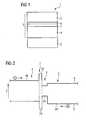
- FIG. 1 shows a schematic sectional view of a first exemplary embodiment of a radiation-emitting semiconductor chip according to the invention.
- the semiconductor chip 1 which is preferably designed as an LED chip, comprises a semiconductor body 3 arranged on a carrier 2.
- the semiconductor body has an n-conducting region 4 and a p-conducting region 5, between which an active region 6 suitable for the generation of radiation is arranged.
- the n-type and / or the p-type region may include a plurality of semiconductor layers (not shown).
- a hole barrier layer 7 Integrated between the n-type region 4 and the active region 6 or in the n-type region.
- the hole barrier layer 7 adjoins or limits the active region 6.
- the hole barrier layer 7 is based on a nitride compound semiconductor material from the material system In y Ga 1-xy Al x N with 0 ⁇ xs 1, 0 ⁇ y ⁇ 1 and x + ys 1 and is formed such that they penetrate holes, which in the operation of the semiconductor chip 1 via the p-type region. 5 into the active zone, reduces or blocks completely.
- the hole barrier layer 7 is designed to be permeable. Electron-hole pairs can recombine in the active region under radiation generation.
- the semiconductor body 3 is preferably grown epitaxially on an epitaxial substrate.
- the carrier 2 can emerge in particular from the epitaxial substrate on which a semiconductor layer sequence has grown for the semiconductor body.
- the semiconductor body is furthermore preferably based on nitride compound semiconductor materials.
- An SiC substrate or a sapphire substrate is particularly suitable here as an epitaxial substrate.
- the semiconductor chip is preferably designed for generating ultraviolet or visible radiation, in particular from the blue to the green spectral range.
- nitride compound semiconductors are particularly suitable.
- the active region 6 is expediently designed in such a way that both the electrons in the conduction band and the holes in the valence band are formed around the active region 6 on both sides of barriers which enclose charge carriers in the active region.
- the internal quantum efficiency of the semiconductor chip can thus be increased.
- one of these barriers is formed by the hole barrier layer, which accordingly may also be formed as an inclusion layer.
- the active region 6 comprises a single or multiple quantum well structure. Such structures are particularly suitable for forming an active region of high internal quantum efficiency.
- quantum well structure encompasses any structure in which charge carriers undergo quantization of their energy states by confinement.
- Name Quantum well structure No information about the dimensionality of the quantization. It thus includes quantum wells, quantum wires and quantum dots and any combination of these structures.
- a potential barrier is preferably formed for the holes, via which the penetration of holes into the n-conducting region is hindered.
- the probability of non-radiative recombination of electrons and holes outside the active region in the n-type region can thus be reduced.
- the internal quantum efficiency of the semiconductor chip can be stabilized even at high current densities.
- the likelihood of penetration of holes directed to the active region via the p-type region would increase to the n-type region 4. The internal quantum efficiency would then be reduced accordingly.
- the potential barrier to be overcome by holes for entry into the n-conducting region 4 is therefore preferably increased with respect to a semiconductor body without a hole barrier layer.
- the barrier height can be influenced by means of the band gap of the hole barrier layer 7 and / or by suitable doping of the hole barrier layer.
- the bandgap e.g. can be adjusted via the aluminum content x of the hole-barrier layer, with increasing aluminum content and the band gap increases.
- An aluminum content x of 0.2 or more is particularly suitable for a hole barrier layer 7.
- the indium content y of the hole Barrier layer 7 preferably greater than 0 selected. If the hole barrier layer 7 contains both indium and aluminum and optionally gallium, then y ⁇ x preferably applies.
- an indium content y which is lower than the aluminum content x, is particularly suitable, in particular for an active region based on In y Ga 1-y N.
- the hole barrier layer can simultaneously be embodied as a buffer layer for the active region 6 and as a barrier layer for holes.
- the aluminum content is preferred, in particular for an indium-free hole barrier layer, less than or equal to 0.45. Tensions can be kept so low.
- the hole barrier layer 7 is designed as a tunnel barrier layer.
- An example of a band diagram for a tunnel barrier layer is shown schematically in FIG. FIG. 2 schematically shows the profile of the conduction band edge 8 and the valence band edge 9 in the semiconductor body 3 of the semiconductor chip, which is preferably operated in the forward direction.
- the conduction band edge 78 of the formed as a tunnel barrier layer hole-barrier layer 7 is energetically above the conduction band edge 48 of the n-type region 4 adjacent to the hole-barrier layer 7 layer.
- the valence band edge 79 of the tunnel barrier layer lies energetically below the valence band edge 69 of the active region and preferably below the valence band edge 59 of the layer adjacent to the active region 6 on the side of the p-type region 5. Electrons coming from the n-type region 4 are guided to the active region 6, as well as holes for penetration into the n-type region must overcome a potential barrier.
- the height of the potential barrier to be overcome for electrons is given by the difference of the energies of the conduction band edge 78 and the conduction band edge 48, the height of the potential barrier for the holes by the difference of the energies of the valence band edge 69 and the valence band edge 79.
- the tunneling probability with which the charge carriers tunnel through the tunnel barrier layer depends on the respective barrier height to be overcome and the thickness of the tunnel barrier layer.
- the tunneling probability T is proportional to T ⁇ exp - 2 ⁇ d ⁇ ⁇ 2 ⁇ m ⁇ V 0 - e with the absolute barrier height V 0 , the barrier thickness d, as well as the energy E of the charge carriers and the effective mass m of the respective charge carriers.
- the barrier height to be overcome by the charge carriers is determined by the difference between the absolute barrier height V 0 -the energy of the conduction or valence band edge of the tunnel barrier layer-and the energy E of the respective charge carriers.
- the barrier height can be adjusted via the band gap, that is to say the difference between the energies of the valence band edge and the conduction band edge of the hole barrier layer 7. As already stated above, this can be done via the aluminum content x.
- FIG. 3 shows the dependence of the tunneling probability 10 for electrons and the tunneling probability 11 for holes as a function of the thickness d of the tunnel barrier layer in nanometers for an Al 0.5 Ga 0.5 N tunnel barrier layer in a diagram.
- Tunneling probabilities were determined based on the above relationship. Because the effective mass of Holes is larger than that of the electrons, the tunneling probability decreases 11 with increasing thickness of the tunnel barrier layer much more than that of the electrons. The effective mass of the holes is about ten times or more the effective mass of the electrons. This results in different tunneling probabilities for electrons and holes, so that charge-carrier asymmetric tunnels (Carrier Asymmetric Tunneling) electrons tunnel through the tunnel barrier layer to a much greater extent than holes. Holes are mostly held by the active region 6 by means of the tunnel barrier layer.
- the tunneling probability of the electrons through the tunnel barrier layer may be ten times or more, preferably one hundred times or more, more preferably a thousand times or more, the tunneling probability of the holes through the tunnel barrier layer. This can be achieved by suitable design of the tunnel barrier layer.
- the thickness of the tunnel barrier layer is 8 nm or less, more preferably 4 nm or less.
- a thickness of greater than or equal to 1 nm has been found to be particularly advantageous.
- x values are particularly suitable between in each case including 0.2 and 0.45, preferably greater than or equal to 0.3. Especially with regard to moderate lattice mismatch tunnel barrier layers with such aluminum content are particularly suitable.
- the tunnel barrier layer can be doped n-type, for example.
- the conduction band edge 78 of the tunnel barrier layer is then lowered, as is the valence band edge 79 of the tunnel barrier layer.
- the band gap remains essentially constant, so that the barrier height for holes is increased while the barrier height for electrons is reduced.
- a dopant with comparatively low donor levels, for example Si, is particularly suitable for this purpose.
- targeted impurities may be incorporated into the tunnel barrier layer that assist in tunneling the electrons to hole tunneling (trap assisted tunneling) and accordingly increase the tunneling probability for electrons relative to that of the holes.
- impurity atom for example, Si is suitable.
- a targeted reduction of the potential barrier for the electrons is indicated by dashed lines in FIG.
- the current density dependence of the internal quantum efficiency can advantageously be reduced since the holes, even at high current densities, increasingly recombine radiatively in the active region 6 and effectively block the penetration of holes into the n-conductive region by means of the tunnel barrier layer becomes.
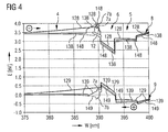
- FIG. 4 shows the influence of the aluminum content on the barrier height of an Al x Ga 1 -x N tunnel barrier layer with x> 0 on the basis of band diagrams determined in a simulation calculation.
- the W direction indicates the growth direction of the semiconductor body in which the individual layers for the semiconductor body, for example epitaxially on an epitaxial substrate, were grown successively.
- the conduction band edge 128 and the valence band edge 129 correspond to a nitride compound semiconductor-based semiconductor body without an aluminum-containing tunnel barrier layer.
- the semiconductor chip with the semiconductor body was assumed to be operated at 3.4 volts in the forward direction.
- the tunnel barrier layer 7b has an aluminum content of 0.3.
- the barrier height of the potential barrier of the tunnel barrier layer increases for electrons as well as for holes with the increasing band gap of the tunnel barrier layer due to the increasing aluminum content.
- the arrow 12 symbolizes a tunneling of the electrons into the active region.
- the hole-barrier layer 7 is designed as a pure hole-barrier layer.
- a pure hole barrier layer in contrast to a tunnel barrier layer, electrons pass from the n-type region 4 into the active region 6 substantially unhindered, that is to say without potential barriers.
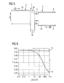
- FIG. 5 shows schematically a band diagram for a pure hole barrier layer.
- the hole barrier layer 7 has a conduction band edge 78 whose energy is less than or equal to that of the conduction band edge 48 of a layer adjoining the pure hole barrier layer 7 on the part of the n-type region 4.
- the valence band edge 79 of the pure hole barrier layer is lower in energy than the valence band edge 69 of the layer adjacent to the active region, and preferably lower in energy than the valence band edge 59 of a layer adjacent to the active region 6 on the part of the p-type region 5.
- the pure hole barrier layer can be made comparatively thick, since tunneling through of electrons does not have to be considered.
- the probability of penetration of holes into the n-type region can thus be kept extremely low, for example less than or equal to 10 -4 or less than or equal to 10 -5 .
- the pure hole barrier layer has an aluminum content between 0.2 and 0.3 inclusive.
- a thickness of the pure hole barrier layer may be between 11 nm and 30 nm inclusive.
- the pure hole barrier layer can also be made thicker.
- the pure hole-barrier layer is preferably more heavily doped (n + ) than a layer arranged on the side of the n-conductive region, in particular adjacent to the hole-barrier layer. Forming an electronically barrier-free transition to the active region can thus be facilitated.
- the conduction band edge 78 of the hole barrier layer may also lie below the conduction band edge 48 in terms of energy. This is indicated by dashed lines in FIG.
- FIG. 6 shows the dependence of the internal quantum efficiency Q in percent of the semiconductor chip 1 on the operating current density j in amperes per square centimeter.
- the current density j is plotted logarithmically.
- the curve 14 was for a semiconductor chip with a semiconductor body based on nitride compound semiconductor determined without aluminum-containing hole barrier layer and the curve 13 for a corresponding semiconductor body with aluminum-containing hole-barrier layer.
- the dependence of the internal quantum efficiency Q on the current density j is greatly reduced in the case of the curve 13 with respect to the curve 14.
- the internal quantum efficiency for the semiconductor chip with the hole barrier layer is substantially constant and independent of the operating current density.
- FIG. 7 shows a schematic sectional view of a second exemplary embodiment of a semiconductor chip 1 according to the invention.
- the semiconductor chip 1 corresponds to the semiconductor chip described in connection with FIG.
- the semiconductor chip 1 shown in FIG. 7 is designed as a thin-film chip.
- the carrier 2 is different from an epitaxial substrate on which a semiconductor layer sequence for the semiconductor body 3 has grown epitaxially.
- the semiconductor body 3 can be manufactured on the epitaxial substrate and subsequently arranged with its side facing away from the epitaxial substrate on the carrier 2 and preferably fixed.
- the carrier 2 does not have to meet the stringent requirements for an epitaxial substrate.
- the epitaxial substrate can be removed so that the thin-film chip is free of an epitaxial substrate. For example, etching, water jet cutting or a laser separation method is suitable for this purpose.
- nitride compound semiconductor-based semiconductor body for example, SiC or sapphire is suitable as a material for the epitaxial substrate.
- the carrier may also contain such materials.
- the carrier may be metallic or ceramic.
- a, in particular metallic, mirror layer 15 is arranged between the carrier 2 and the semiconductor body 3.
- This can prevent absorption in the active region 6 of generated radiation in a possibly absorbing carrier by reflection of the radiation at the mirror layer.
- the radiation component emerging from the semiconductor body 3 via the main surface 16 remote from the carrier can be increased due to the mirror layer.
- a connecting layer 17 is preferably arranged, by means of which the semiconductor body 3 is fixed on the carrier 2.
- the bonding layer 17 may be implemented, for example, as a solder layer or a layer formed in a wafer bonding process.
- the connection layer 17, the mirror layer 15 and / or the carrier 2 is designed to be electrically conductive.
- connection layer 17, the mirror layer 15 and / or the carrier 2 is electrically conductively connected to the active region 6.
- the active region 6 can thus be electrically contacted by means of a contact layer (not shown) arranged on the side of the carrier facing away from the semiconductor body.
- a corresponding mating contact layer (not shown) may be disposed on the main surface 16.
- This contact layer (s) is (are) preferably made metallic.
- the mirror layer 15 preferably contains Al, Ag, Pt or an alloy with at least one of these materials. These materials can advantageously have high reflectivities in the spectral ranges mentioned.
- the hole barrier layer 7 is in the case of the thin-film chip on the side of the active region 6 facing away from the carrier 2 arranged, since the semiconductor body after completion of the growth with the p-type region 5 has been arranged on the support 2.
- the hole barrier layer may be formed according to the above embodiments, wherein the efficiency, in particular the Auskoppeleffizienz, the semiconductor chip due to the mirror layer and the relatively free choice of the carrier may be advantageously increased.
- a hole barrier layer according to the invention can be applied not only to LED chips, but also to optical cavity laser chips such as an edge emitting laser chip, an internal cavity VCSEL, a Vertical External Cylinder Surface Emitting Laser (VECSEL). with external resonator or a RCLED (Resonant Cavity Light Emitting Diode) can be used.
- optical cavity laser chips such as an edge emitting laser chip, an internal cavity VCSEL, a Vertical External Cylinder Surface Emitting Laser (VECSEL). with external resonator or a RCLED (Resonant Cavity Light Emitting Diode) can be used.
Abstract
Description
Die vorliegende Erfindung betrifft einen strahlungsemittierenden Halbleiterchip mit einem zur Strahlungserzeugung geeigneten aktiven Bereich.The present invention relates to a radiation-emitting semiconductor chip with an active region suitable for generating radiation.
Diese Patentanmeldung beansprucht die Priorität der deutschen Patentanmeldungen
Die interne Quanteneffizienz von Halbleiterchips bei der Strahlungserzeugung, insbesondere solchen, die auf Nitrid-Verbindungshalbleitermaterialen basieren, hängt oftmals maßgeblich von der Betriebsstromdichte ab, mit der der Halbleiterchip betrieben wird. Unter interner Quanteneffizienz wird hierbei das Verhältnis der Anzahl an in den aktiven Bereich injizierter Ladungsträger eines Typs - Elektronen oder Löcher - zur Anzahl der hieraus im aktiven Bereich erzeugten Photonen verstanden.The internal quantum efficiency of semiconductor chips in radiation generation, especially those based on nitride compound semiconductor materials, often depends largely on the operating current density with which the semiconductor chip is operated. Internal quantum efficiency is understood to be the ratio of the number of charge carriers injected in the active region of one type-electrons or holes-to the number of photons generated therefrom in the active region.
Je größer die Betriebsstromdichte, desto geringer ist oftmals, insbesondere bei Halbleiterchips auf Nitrid-Basis, die interne Quanteneffizienz. Ein effizienterer Betrieb von Halbleiterchips bei hohen Stromdichten würde es erleichtern, kostengünstig, ohne Vergrößerung der aktiven Fläche, das heißt der Fläche des aktiven Bereichs des Chips, mit diesem Halbleiterchip eine erhöhte Strahlungsleistung zu erzeugen.The larger the operating current density, the lower is often the internal quantum efficiency, in particular with nitride-based semiconductor chips. More efficient operation of semiconductor chips at high current densities would make it easier to inexpensively generate increased radiant power without increasing the active area, that is, the area of the active area of the chip, with this semiconductor chip.
Eine Aufgabe der vorliegenden Erfindung ist es, einen Halbleiterchip anzugeben der vereinfacht mit einer verringerten Abhängigkeit der internen Quanteneffizienz von der Betriebsstromdichte ausbildbar ist.An object of the present invention is to provide a semiconductor chip which can be formed in a simplified manner with a reduced dependence of the internal quantum efficiency on the operating current density.
Diese Aufgabe wird erfindungsgemäß durch einen Halbleiterchip mit den Merkmalen des Patentanspruchs 1 gelöst. Vorteilhafte Weiterbildungen und Ausgestaltungen der Erfindung sind Gegenstand der abhängigen Patentansprüche.This object is achieved by a semiconductor chip with the features of
Ein erfindungsgemäßer strahlungsemittierender Halbleiterchip umfasst einen Halbleiterkörper, der einen n-leitenden Bereich und einen p-leitenden Bereich aufweist, wobei zwischen dem n-leitenden Bereich und dem p-leitenden Bereich ein zur Strahlungserzeugung geeigneter aktiver Bereich angeordnet ist, in dem über den n-leitenden Bereich in den aktiven Bereich geführte Elektronen und über den p-leitenden Bereich in den aktiven Bereich geführte Löcher unter Strahlungserzeugung rekombinieren. Auf der dem p-leitenden Bereich gegenüberliegenden Seite des aktiven Bereichs des erfindungsgemäßen Halbleiterchips ist eine Löcher-Barriereschicht angeordnet, die ein Material aus dem III-V-Halbleitermaterialsystem InyGa1-x-yAlxN mit 0 ≤ x s 1, 0 s y s 1 und x + y s 1 enthält und für die Elektronen durchlässig ist. Die Löcher-Barriereschicht ist hierbei bevorzugt derart im Halbleiterkörper angeordnet und derart ausgebildet, dass sie ein Eindringen von Löchern in den n-leitenden Bereich mindert oder vollständig blockiert.A radiation-emitting semiconductor chip according to the invention comprises a semiconductor body which has an n-conducting region and a p-conducting region, wherein an active region suitable for generating radiation is arranged between the n-conducting region and the p-conducting region, in which region over the n-conducting region. Conducted region in the active region guided electrons and recombine holes guided over the p-type region into the active region under radiation generation. On the side of the active region of the semiconductor chip according to the invention which is opposite the p-type region, a hole barrier layer comprising a material of the III-V semiconductor material system In y Ga 1-xy Al x N with 0
Die Löcher-Barriereschicht behindert also das Eindringen von Löchern in den n-leitenden Bereich und vermindert somit die Wahrscheinlichkeit, dass Löcher im n-leitenden Bereich mit Elektronen nicht-strahlend rekombinieren. Die Wahrscheinlichkeit das Löcher im aktiven Bereich strahlend rekombinieren wird dementsprechend erhöht, da die Löcher mittels der Löcher-Barriereschicht vermehrt auf der dem aktiven Bereich zugewandten Seite der Löcher-Barriereschicht gehalten werden. Insbesondere können Löcher auf diese Weise auch für hohe Stromdichten vermehrt auf der dem aktiven Bereich zugewandten Seite der Löcher-Barriereschicht gehalten werden. Die interne Quanteneffizienz kann mittels der Löcher-Barriereschicht demnach vorteilhaft erhöht werden. Die Abhängigkeit der internen Quanteneffizienz von der Betriebsstromdichte wird mittels der Löcher-Barriereschicht mit Vorteil verringert. Dies äußert sich bei vergleichsweise hohen Stromdichten in besonderem Maße, da die Eintrittswahrscheinlichkeit von Löchern in den n-leitenden Bereichen mit wachsender Betriebsstromdichte in der Regel stark und nichtlinear zunimmt.The hole barrier layer thus hinders the penetration of holes into the n-type region and thus reduces the probability that holes in the n-type region will recombine with non-radiative electrons. The probability that recombine holes in the active area radiant is increased accordingly, since the holes are increasingly held by means of the hole-barrier layer on the active area facing side of the hole-barrier layer. In particular, holes can be kept in this way, even for high current densities increasingly on the active area facing side of the hole-barrier layer. The internal quantum efficiency can therefore advantageously be increased by means of the hole barrier layer. The Dependence of the internal quantum efficiency on the operating current density is advantageously reduced by means of the hole barrier layer. This manifests itself with comparatively high current densities to a particular extent, since the probability of occurrence of holes in the n-type regions generally increases strongly and nonlinearly with increasing operating current density.
Die Löcher-Barriereschicht ist bevorzugt derart ausgebildet, dass die Durchtrittswahrscheinlichkeit von Elektronen durch die Löcher-Barriereschicht größer ist als die Durchtrittswahrscheinlichkeit der Löcher durch die Löcher-Barriereschicht. Eine Barriere für den Durchtritt von Elektronen durch die Löcher-Barriereschicht ist hierzu vorzugsweise kleiner als eine Barriere für den Durchtritt von Löchern durch die Löcher-Barriereschicht.The hole barrier layer is preferably formed in such a way that the probability of the passage of electrons through the hole barrier layer is greater than the probability of the passage of the holes through the hole barrier layer. A barrier for the passage of electrons through the hole-barrier layer is for this purpose preferably smaller than a barrier for the passage of holes through the hole-barrier layer.
Dies kann durch geeignete Ausbildung der Löcher-Barriereschicht erreicht werden. Beispielsweise wird mittels der Löcher-Barriereschicht eine Potenzial-Barriere für die Löcher gebildet. Je höher diese Potenzial-Barriere ist, desto geringer ist in der Regel die Durchtrittswahrscheinlichkeit der Löcher. Weiterhin verringert sich die Durchtrittswahrscheinlichkeit in der Regel auch mit wachsender Dicke der Löcher-Barriereschicht. Die Potenzial-Barriere kann mittels einer Bandlücke der Löcher-Barriereschicht eingestellt werden. Gegebenenfalls kann die Potenzial-Barriere für die Löcher durch geeignete Dotierung, insbesondere durch geeignete n-leitende Dotierung, erhöht werden, wobei besonders bevorzugt die Potenzial-Barriere für Elektronen zugleich vermindert wird.This can be achieved by suitable formation of the hole-barrier layer. For example, a potential barrier is formed for the holes by means of the hole barrier layer. The higher this potential barrier is, the lower is the probability of penetration of the holes. Furthermore, the probability of penetration generally also decreases with increasing thickness of the hole-barrier layer. The potential barrier can be adjusted by means of a band gap of the hole barrier layer. Optionally, the potential barrier for the holes can be increased by suitable doping, in particular by suitable n-type doping, wherein the potential barrier for electrons is particularly preferably reduced at the same time.
Das Verhältnis der Durchtrittswahrscheinlichkeit der Elektronen durch die Löcher-Barriereschicht zu derjenigen der Löcher kann beispielsweise 1/10 oder weniger, bevorzugt 1/100 oder weniger, besonders bevorzugt 1/1000 oder weniger betragen. Je kleiner dieses Verhältnis ist, desto geringer ist die Gefahr, dass die Löcher-Barriereschicht durch Blockade der Elektronen die interne Quanteneffizienz aufgrund der dann verringerten, zum aktiven Bereich gelangenden Anzahl von Elektronen vermindert.The ratio of the passage probability of the electrons through the hole barrier layer to that of the holes may be, for example, 1/10 or less, preferably 1/100 or less, more preferably 1/1000 or less. The smaller this ratio is, the lower is the danger that the hole-barrier layer reduces the internal quantum efficiency by blocking the electrons due to the then reduced, reaching the active region number of electrons.
Bevorzugt ist die Löcher-Barriereschicht zwischen dem n-leitenden Bereich und dem aktiven Bereich angeordnet. Das Eindringen von Löchern in den n-leitenden Bereich kann mittels einer derartigen Anordnung besonders effektiv vermindert werden. Die Löcher-Barriereschicht kann intrinsisch, das heißt undotiert, ausgeführt sein. Eine nichtdotierte Schicht kann gegenüber einer dotierten Schicht gegebenenfalls vereinfacht gefertigt sein. Alternativ kann die Löcher-Barriereschicht jedoch auch dotiert, insbesondere n-leitend dotiert, ausgeführt sein. Zweckmäßigerweise ist die Löcher-Barriereschicht dann im n-leitenden Bereich integriert.Preferably, the hole barrier layer is disposed between the n-type region and the active region. The penetration of holes into the n-type region can be particularly effectively reduced by means of such an arrangement. The hole barrier layer may be intrinsically, that is undoped, executed. A non-doped layer may optionally be made simpler than a doped layer. Alternatively, however, the hole-barrier layer may also be doped, in particular n-doped. Conveniently, the hole barrier layer is then integrated in the n-type region.
Eine Anordnung der Löcher-Barriereschicht auf einer dem aktiven Bereich zugewandten Seite des n-leitenden Bereichs im n-leitenden Bereich ist für eine Löcherbarriere ferner besonders zweckmäßig. Bevorzugt ist der n-leitende Bereich durch die Löcher-Barriereschicht seitens des aktiven Bereichs begrenzt.An arrangement of the hole barrier layer on an active region side of the n-type region in the n-type region is also particularly useful for a hole barrier. Preferably, the n-type region is bounded by the hole-barrier layer on the part of the active region.
Weiterhin grenzt die Löcher-Barriereschicht bevorzugt an den aktiven Bereich an oder die Löcher-Barriereschicht begrenzt den aktiven Bereich. Im letzteren Fall kann die Löcher-Barriereschicht beispielsweise zugleich als Einschlussschicht für den aktiven Bereich dienen, mittels derer Ladungsträger im aktiven Bereich eingeschlossen werden können (Confinement). Eine Anordnung der Löcher-Barriereschicht möglichst nahe am aktiven Bereich ist für eine Löcher-Barriereschicht besonders vorteilhaft.Furthermore, the hole-barrier layer preferably adjoins the active area or the hole-barrier layer delimits the active area. In the latter case, for example, the hole barrier layer can simultaneously serve as an inclusion layer for the active region, by means of which charge carriers can be confined in the active region (confinement). An arrangement of the hole-barrier layer as close as possible to the active region is particularly advantageous for a hole-barrier layer.
In einer bevorzugten Ausgestaltung ist der Aluminiumgehalt x in der Löcher-Barriereschicht größer 0. Mittels des Aluminiumgehalts kann die Bandlücke der Löcher-Barriereschicht eingestellt und hierüber die Höhe der resultierenden Potenzial-Barriere für die Löcher bestimmt werden. Je größer der Aluminiumgehalt ist, desto größer ist in der Regel die Bandlücke der Löcher-Barriereschicht. Mit der Bandlücke wächst in der Regel auch die Barrierenhöhe.In a preferred embodiment, the aluminum content x in the hole-barrier layer is greater than 0. By means of Alumina content, the band gap of the hole-barrier layer can be set and used to determine the height of the resulting potential barrier for the holes. The larger the aluminum content, the larger the bandgap of the hole barrier layer is, as a rule. As a rule, the band gap also increases the barrier height.
Bevorzugt ist der Aluminiumgehalt x größer oder gleich 0,2, besonders bevorzugt größer oder gleich 0,5, zum Beispiel bis 1. Mit derartigen Aluminiumgehalten kann eine effiziente Löcherblockade mittels der Löcher-Barriereschicht, insbesondere in einem auf Nitrid-Verbindungshalbleitern basierenden Halbleiterkörper, erreicht werden.The aluminum content x is preferably greater than or equal to 0.2, particularly preferably greater than or equal to 0.5, for example up to 1. With such aluminum contents, efficient hole blockage can be achieved by means of the hole barrier layer, in particular in a semiconductor body based on nitride compound semiconductors become.
Mit wachsendem Aluminiumgehalt verringert sich jedoch in der Regel auch die Gitterkonstante der Löcher-Barriereschicht. Insbesondere gilt dies für eine indiumfreie Löcher-Barriereschicht mit y = 0. Hieraus können tensile Verspannungen im Halbleiterkörper resultieren. Derartige Verspannungen im Halbleiterkörper, insbesondere im aktiven Bereich, können wiederum zu,einer Verringerung der internen Quanteneffizienz des Halbleiterchips führen. Insbesondere gilt dies für einen aktiven Bereich, der eine Schicht aus dem III-V-Halbleitermaterialsystem InyGa1-yN mit 0 < y s 1 enthält oder auf diesem Materialsystem basiert. Eine Schicht aus diesem Materialsystem ist aluminiumfrei. Die Gitterfehlanpassung einer derartigen Schicht zu einer aluminiumhaltigen Schicht kann daher in erhöhtem Maße zu Verspannungen im Halbleiterkörper, insbesondere dem aktiven Bereich, führen. Um die aufgrund der Löcher-Barriereschicht im Halbleiterkörper resultierende Verspannung tolerabel gering zu halten, ist x bevorzugt kleiner oder gleich 0,45. Von besonderer Bedeutung ist dies, falls die Löcher-Barriereschicht indiumfrei mit y = 0 ausgebildet ist.As the aluminum content increases, however, the lattice constant of the hole-barrier layer generally also decreases. This applies in particular to an indium-free hole barrier layer with y = 0. From this, tensile stresses in the semiconductor body can result. Such stresses in the semiconductor body, in particular in the active region, can in turn lead to a reduction in the internal quantum efficiency of the semiconductor chip. In particular, this applies to an active region which contains a layer of the III-V semiconductor material system In y Ga 1-y N with 0 <
Ist die Löcher-Barriereschicht indiumhaltig, das heißt mit y größer 0, ausgebildet, so können mit Vorteil die Gitterkonstante und die Bandlücke der Löcher-Barriereschicht über Variation des Indiumgehalts y und des Aluminiumgehalts x im wesentlichen unabhängig voneinander eingestellt werden.If the hole barrier layer indiumhaltig, that is formed with y greater than 0, so can with advantage the Lattice constant and the band gap of the hole barrier layer on variation of the indium content y and the aluminum content x are set substantially independently.
Die Löcher-Barriereschicht kann somit als Pufferschicht ausgebildet sein. Über die Pufferschicht kann beim Herstellen des Halbleiterkörpers, beispielsweise mittels epitaktischen Aufwachsens, die Gitterkonstante für auf die Pufferschicht aufzubringende weitere Halbleiterschichten optimiert werden. Verspannungen können so reduziert werden. Bevorzugt ist die Löcher-Barriereschicht als Pufferschicht für die Schicht(en) für den aktiven Bereich ausgebildet. Einer Effizienzminderung des aktiven Bereichs, insbesondere eines aktiven Bereichs auf InGaN-Basis, kann so vorgebeugt werden. Bevorzugt ist hierbei 0 < y < x, besonders bevorzugt 0 < y < x ≤ 1. Der aufgrund des vergleichsweise hohen Aluminiumsgehalts x vereinfacht auftretenden tensilen Verspannung kann mit Vorteil mit einem gegenüber dem Aluminiumgehalt x geringeren Indiumgehalt y bereits ausreichend entgegengewirkt werden. Bevorzugt wird eine Verspannung vollständig vermieden. Eine indiumfreie, aluminiumhaltige Löcher-Barriereschicht ist jedoch gegenüber einer indium- und aluminiumhaltigen Löcher-Barriereschicht vereinfacht herstellbar.The hole barrier layer can thus be formed as a buffer layer. During the production of the semiconductor body, for example by means of epitaxial growth, the lattice constant for further semiconductor layers to be applied to the buffer layer can be optimized via the buffer layer. Tension can be reduced. Preferably, the hole barrier layer is formed as a buffer layer for the active region layer (s). An efficiency reduction of the active area, in particular an active area based on InGaN, can thus be prevented. In this case, 0 <y <x, particularly preferably 0 <y <x <1, is preferred. The tensile stress which occurs in a simplified manner due to the comparatively high aluminum content x can already be sufficiently counteracted with a lower indium content y compared to the aluminum content x. Preferably, a tension is completely avoided. However, an indium-free, aluminum-containing hole barrier layer can be produced more easily than an indium- and aluminum-containing hole barrier layer.
In einer weiteren bevorzugten Ausgestaltung ist die Löcher-Barriereschicht als Tunnel-Barriereschicht ausgeführt, wobei die Tunnel-Barriereschicht derart ausgebildet ist, dass sie von den Elektronen mit höherer Wahrscheinlichkeit durchtunnelt wird, als von den Löchern. Mittels der Tunnel-Barriereschicht wird sowohl für die Elektronen, als auch für Löcher eine Potenzial-Barriere ausgebildet, wobei die jeweilige Potenzial-Barriere von Elektronen vor dem Eindringen in den aktiven Bereich und von Löchern vor dem Eindringen in den n-leitenden Bereich zu überwinden ist.In a further preferred embodiment, the hole barrier layer is designed as a tunnel barrier layer, wherein the tunnel barrier layer is designed such that it is more likely to be tunneled through by the electrons, as from the holes. By means of the tunnel barrier layer, a potential barrier is formed for both the electrons and holes, whereby the respective potential barrier of electrons to overcome before penetrating into the active region and holes before the penetration into the n-type region is.
Die Energie der Leitungsbandkante der Tunnel-Barriereschicht ist bevorzugt größer als die Energie der Leitungsbandkante einer seitens des n-leitenden Bereichs an die Tunnel-Barriereschicht angrenzende Schicht. Die Differenz dieser Energien bestimmt die maximale Barrierenhöhe der von den Elektronen vor dem Eindringen in den aktiven Bereich zu überwindenden Potenzial-Barriere.The energy of the conduction band edge of the tunnel barrier layer is preferably greater than the energy of the conduction band edge a layer adjacent to the tunnel barrier layer from the n-type region. The difference of these energies determines the maximum barrier height of the potential barrier to be overcome by the electrons before entering the active region.
Die Energie der Valenzbandkante der Tunnel-Barriereschicht ist bevorzugt kleiner als die Energie der Valenzbandkante einer auf der dem n-leitenden Bereich gegenüber liegenden Seite der Tunnel-Barriereschicht angeordneten, insbesondere an die Tunnel-Barriereschicht angrenzenden Schicht, zum Beispiel einer Schicht des aktiven Bereichs. Die Differenz dieser Energien bestimmt die maximale Barrierenhöhe der von den Löchern vor dem Eindringen in den n-leitenden Bereich zu überwindenden Potenzial-Barriere.The energy of the valence band edge of the tunnel barrier layer is preferably smaller than the energy of the valence band edge of a layer arranged on the side of the tunnel barrier layer opposite the n-conductive region, in particular adjacent to the tunnel barrier layer, for example a layer of the active region. The difference in these energies determines the maximum barrier height of the potential barrier to be overcome by the holes before entering the n-type region.
Eine Bandlücke der Tunnel-Barriereschicht ist weiterhin bevorzugt größer als die Bandlücke einer seitens des n-leitenden Bereichs und/oder einer auf der dem n-leitenden Bereich gegenüberliegenden Seite im Halbleiterkörper an die Tunnel-Barriereschicht angrenzenden Schicht. Das Ausbilden einer Barriere für Elektronen und Löcher wird so erleichtert.A band gap of the tunnel barrier layer is furthermore preferably larger than the band gap of a layer adjacent to the tunnel barrier layer on the side of the n-conducting region and / or on the side opposite the n-conducting region in the semiconductor body. The formation of a barrier for electrons and holes is thus facilitated.
Die Tunnelwahrscheinlichkeit hängt von der Barrierenhöhe und der Barrierendicke ab. Je dicker die Tunnel-Barriereschicht beziehungsweise je höher die Potenzial-Barriere ist, desto geringer ist in der Regel die Tunnelwahrscheinlichkeit. Die Tunnelwahrscheinlichkeit wird weiterhin durch die effektive Masse der Ladungsträger bestimmt, wobei die Tunnelwahrscheinlichkeit in der Regel mit wachsender effektiver Masse abnimmt. Da die Löcher regelmäßig eine effektive Masse größer derjenigen der Elektronen aufweisen, ist die Tunnelwahrscheinlichkeit der Löcher häufig geringer als die der Elektronen.The tunneling probability depends on the barrier height and the barrier thickness. The thicker the tunnel barrier layer or the higher the potential barrier, the lower is the tunneling probability as a rule. The tunneling probability is further determined by the effective mass of the charge carriers, the tunneling probability generally decreasing with increasing effective mass. Since the holes regularly have an effective mass larger than that of the electrons, the tunneling probability of the holes is often lower than that of the electrons.
Bevorzugt weist die Tunnel-Barriereschicht eine Dicke von 8 nm oder weniger, besonders bevorzugt von 4 nm oder weniger, auf. Weiterhin ist bevorzugt 0,2 ≤ x s 0,45. Mittels derartiger Tunnel-Barriereschichten kann eine Tunnelbarriere ausgebildet werden, die ein Eindringen von Löchern in den n-leitenden Bereich effizient mindert und das Durchtreten von Elektronen vom n-leitenden Bereich in den aktiven Bereich nur moderat behindert. Weiterhin kann eine Verspannung im Halbleiterkörper über eine Wahl des Aluminiumgehalts im oben angeführten Bereich vergleichsweise gering gehalten werden. Besonders bevorzugt ist der Aluminiumgehalt für eine Tunnelbarriereschicht größer oder gleich 0,3.Preferably, the tunnel barrier layer has a thickness of 8 nm or less, more preferably 4 nm or less, on. Furthermore, it is preferably 0.2 ≦ xs 0.45. By means of such tunnel barrier layers, a tunnel barrier can be formed which effectively reduces the penetration of holes into the n-type region and only moderately impedes the passage of electrons from the n-type region into the active region. Furthermore, a strain in the semiconductor body can be kept comparatively low via a choice of the aluminum content in the above-mentioned range. Particularly preferably, the aluminum content for a tunnel barrier layer is greater than or equal to 0.3.
Die Tunnel-Barriereschicht kann n-leitend dotiert oder intrinsisch ausgeführt sein. Über n-leitende Dotierung, zum Beispiel mittels Si, kann die Barrierenhöhe für Elektronen abgesenkt werden. Aufgrund der bei der Dotierung im wesentlichen konstant bleibenden Bandlücke wird die Barriere für die Löcher hierüber zugleich erhöht. Eine undotierte Schicht ist gegenüber einer dotierten Schicht vereinfacht herstellbar. Weiterhin können Störstellen in die Tunnel-Barriereschicht eingebaut werden, die das Tunneln der Elektronen assistieren und die Tunnelwahrscheinlichkeit der Elektronen gegenüber der der Löcher erhöhen. Als Störstellenatom eignet sich beispielsweise Si.The tunnel barrier layer may be n-type doped or intrinsic. Via n-type doping, for example by means of Si, the barrier height for electrons can be lowered. Due to the band gap which remains substantially constant during the doping, the barrier for the holes over this is simultaneously increased. An undoped layer can be produced in a simplified manner compared to a doped layer. Furthermore, impurities can be incorporated into the tunnel barrier layer, which assist the tunneling of the electrons and increase the tunneling probability of the electrons relative to the holes. As an impurity atom, for example, Si is suitable.
In einer weiteren bevorzugten Ausgestaltung ist die Löcher-Barriereschicht als reine Löcher-Barriereschicht ausgebildet, die ein Durchtreten von Löchern, insbesondere vollständig, blockiert. Bevorzugt ist die reine Löcher-Barriereschicht für die Elektronen im wesentlichen vollständig durchlässig. Die reine Löcher-Barriereschicht bildet weiterhin mit Vorzug eine Potenzial-Barriere für die Löcher aus, während, im Gegensatz zu einer Tunnel-Barriereschicht, die Elektronen im wesentlichen potenzialbarrierefrei durch die reine Löcher-Barriereschicht hindurchtreten. Aufgrund des ungehinderten Durchtritts der Elektronen durch die reine Löcherbarriereschicht kann verglichen mit einer Tunnel-Barriereschicht die interne Quanteneffizienz des Halbleiterchips erhöht sein.In a further preferred embodiment, the hole-barrier layer is formed as a pure hole-barrier layer, which blocks passage of holes, in particular completely. Preferably, the pure hole barrier layer for the electrons is substantially completely permeable. The pure hole barrier layer also preferentially forms a potential barrier to the holes while, unlike a tunnel barrier layer, the electrons pass substantially barrier free through the pure hole barrier layer. Due to the unimpeded passage of the electrons through the pure hole barrier layer can be compared with a tunnel barrier layer the internal quantum efficiency of the semiconductor chip can be increased.
Bevorzugt ist die reine Löcher-Barriereschicht derart n-leitend dotiert, dass die Energie der Leitungsbandkante der Löcher-Barriereschicht kleiner oder gleich der Energie der Leitungsbandkante einer auf der dem aktiven Bereich gegenüberliegenden Seite der reinen Löcher-Barriereschicht an die reine Löcher-Barriereschicht angrenzenden Schicht ist. Als Donator ist beispielsweise Si geeignet.The pure hole barrier layer is preferably n-doped such that the energy of the conduction band edge of the hole barrier layer is less than or equal to the energy of the conduction band edge of a layer adjacent to the active region of the pure hole barrier layer adjacent to the pure hole barrier layer is. For example, Si is suitable as donor.
Die reine Löcher-Barriereschicht kann insbesondere eine derart hohe Potenzial-Barriere und/oder Dicke aufweisen, dass Elektronen, falls mittels der Löcher-Barriereschicht auch eine Elektronen-Barriere gebildet wäre, diese nicht oder nur mit einer Wahrscheinlichkeit von 10-5 oder weniger durchdringen würden. Für eine vollständig durchlässige Schicht wäre die Durchtrittswahrscheinlichkeit gleich 1.In particular, the pure hole barrier layer may have such a high potential barrier and / or thickness that, if an electron barrier was also formed by the hole barrier layer, electrons would not penetrate it, or only with a probability of 10 -5 or less would. For a completely transmissive layer, the probability of occurrence would be 1.
Bevorzugt weist die reine Löcher-Barriereschicht eine Dicke von 11 nm oder mehr auf. Weiterhin weist die reine Löcher-Barriereschicht bevorzugt eine Dicke von 30 nm oder weniger auf. Eine reine Löcher-Barriereschicht einer derartigen Dicke hat sich zur effizienten Blockade des Eindringens von Löchern in den n-leitenden Bereich als besonders geeignet erwiesen. Die Löcher-Barriereschicht kann natürlich auch mit einer Dicke von mehr als 30 nm ausgeführt sein, wobei die Barrierewirkung durch Vergrößerung dieser Dicke nicht maßgeblich verstärkt wird.Preferably, the pure hole barrier layer has a thickness of 11 nm or more. Furthermore, the pure hole-barrier layer preferably has a thickness of 30 nm or less. A pure hole barrier layer of such thickness has been found to be particularly suitable for efficiently blocking the penetration of holes into the n-type region. Of course, the hole barrier layer can also be made with a thickness of more than 30 nm, wherein the barrier effect is not significantly enhanced by increasing this thickness.
Ferner hat sich ein Aluminiumgehalt mit 0,2 ≤ x ≤ 0,3 für eine reine Löcher-Barriereschicht als besonders zweckmäßig erwiesen.Further, an aluminum content of 0.2 ≦ x ≦ 0.3 has been found to be particularly useful for a pure hole barrier layer.
In einer weiteren bevorzugten Ausgestaltung ist der Halbleiterkörper auf einem Träger angeordnet. Der Halbleiterchip umfasst dann den Träger mit dem auf diesem angeordneten Halbleiterkörper. Der Träger kann den Halbleiterkörper, der vorzugsweise eine Halbleiterschichtenfolge mit einer Mehrzahl von Halbleiterschichten aufweist, mechanisch stabilisieren.In a further preferred embodiment, the semiconductor body is arranged on a carrier. The semiconductor chip then includes the carrier with the on this arranged semiconductor body. The carrier may mechanically stabilize the semiconductor body, which preferably has a semiconductor layer sequence with a plurality of semiconductor layers.
Beispielsweise kann der Träger aus einem Epitaxiesubstrat, auf dem der Halbleiterkörper epitaktisch gewachsen ist, gebildet sein. Der Träger kann jedoch auch von dem Epitaxiesubstrat verschieden sein. Ist der Träger vom Epitaxiesubstrat verschieden, so wird der Halbleiterchip auch als Dünnfilm-Chip bezeichnet. Für Dünnfilm-Chips wird der Halbleiterkörper bevorzugt zunächst auf dem Epitaxiesubstrat gewachsen. Nachfolgend wird der Halbleiterkörper, bevorzugt auf der dem Epitaxiesubstrat abgewandten Seite, auf dem Träger angeordnet und vorzugsweise befestigt. Daraufhin wird das Epitaxiesubstrat, beispielsweise über Ätzen oder ein Lasertrennverfahren, abgelöst. Eine mechanische Unterstützung des Halbleiterkörpers wird durch den Träger gewährleistet.By way of example, the carrier can be formed from an epitaxial substrate on which the semiconductor body has grown epitaxially. However, the carrier may also be different from the epitaxial substrate. If the carrier is different from the epitaxial substrate, the semiconductor chip is also referred to as a thin-film chip. For thin-film chips, the semiconductor body is preferably first grown on the epitaxial substrate. Subsequently, the semiconductor body, preferably on the side remote from the epitaxial substrate, is arranged on the carrier and preferably fixed. Then the epitaxial substrate is removed, for example by etching or a laser separation process. Mechanical support of the semiconductor body is ensured by the carrier.
Bei Dünnfilm-Chips ist die Löcher-Barriereschicht bevorzugt auf der dem Träger gegenüberliegenden Seite des aktiven Bereichs angeordnet, während die Löcher-Barriereschicht bei Nicht-Dünnfilm-Chips bevorzugt zwischen dem aktiven Bereich und dem Träger angeordnet ist. Eine derartige Anordnung ergibt sich insbesondere dann, wenn zuerst der n-leitende Bereich des Halbleiterkörpers auf dem Epitaxiesubstrat gewachsen wird. Der p-leitende Bereich ist dann auf der dem Epitaxiesubstrat abgewandten Seite des aktiven Bereichs angeordnet und wird bei der Ausbildung eines Dünnfilm-Chips demgemäß auf der Seite des Trägers angeordnet, sodass der aktive Bereich zwischen der Löcher-Barriereschicht und dem Träger angeordnet ist.In the case of thin-film chips, the hole-barrier layer is preferably arranged on the side of the active region opposite the carrier, while the hole-barrier layer is preferably arranged between the active region and the carrier in the case of non-thin-film chips. Such an arrangement results in particular when first the n-type region of the semiconductor body is grown on the epitaxial substrate. The p-type region is then arranged on the side of the active region which faces away from the epitaxial substrate and, when a thin-film chip is formed, is accordingly arranged on the side of the carrier so that the active region is arranged between the hole-barrier layer and the carrier.
Für Dünnfilm-Chips kann der Träger gegenüber einem Epitaxiesubstrat vergleichsweise frei gewählt werden, da die Anforderungen an einen Träger für einen Dünnfilm-Chip in der Regel geringer sind als diejenigen, denen ein Epitaxiesubstrat, etwa hinsichtlich dessen Kristallstruktur, unterliegt. Der Träger kann beispielsweise hinsichtlich optimierter Wärme- und/oder elektrischer Leitfähigkeit gewählt werden.For thin-film chips, the carrier can be chosen comparatively freely with respect to an epitaxial substrate, since the requirements for a carrier for a thin-film chip are generally lower than those for a thin film chip Epitaxial substrate, about as regards its crystal structure, subject. The carrier can be selected, for example, with regard to optimized thermal and / or electrical conductivity.
Ein Dünnfilm-Chip, insbesondere ein Dünnfilm-Leuchtdioden-Chip, kann sich weiterhin durch mindestens eines der folgenden charakteristischen Merkmale auszeichnen:
- an einer zu dem Träger hin gewandten Hauptfläche des Halbleiterkörpers, der bevorzugt eine Epitaxieschichtenfolge aufweist, ist eine reflektierende Schicht aufgebracht oder ausgebildet, die zumindest einen Teil der im Halbleiterkörper erzeugten elektromagnetischen Strahlung in diesen zurückreflektiert,
- der Halbleiterkörper, insbesondere die Epitaxieschichtenfolge, weist eine Dicke im Bereich von 20µm oder weniger, insbesondere
im Bereich von 10 µm auf, und/oder - der Halbleiterkörper, insbesondere die Epitaxieschichtenfolge, enthält mindestens eine Halbleiterschicht mit zumindest einer Fläche, die eine Durchmischungsstruktur aufweist, die im Idealfall zu einer annähernd ergodischen Verteilung des Lichtes im Halbleiterkörper, insbesondere in der Epitaxieschichtenfolge, führt, d.h. die Durchmischungsstruktur weist ein möglichst ergodisch stochastisches Streuverhalten auf.
- on a main surface of the semiconductor body which faces towards the carrier and which preferably has an epitaxial layer sequence, a reflective layer is applied or formed which reflects back at least part of the electromagnetic radiation generated in the semiconductor body,
- the semiconductor body, in particular the epitaxial layer sequence, has a thickness in the range of 20 μm or less, in particular in the range of 10 μm, and / or
- the semiconductor body, in particular the epitaxial layer sequence, contains at least one semiconductor layer with at least one surface which has a thorough mixing structure which ideally leads to an approximately ergodic distribution of the light in the semiconductor body, in particular in the epitaxial layer sequence, ie the mixed structure has a preferably ergodically stochastic scattering behavior on.
Ein Grundprinzip eines Dünnschicht-Leuchtdiodenchips ist beispielsweise in
Bevorzugt ist zwischen dem Träger und dem aktiven Bereich, besonders bevorzugt zwischen dem Halbleiterkörper und dem Träger, eine Spiegelschicht angeordnet. Die Spiegelschicht kann im aktiven Bereich erzeugte Strahlung reflektieren und somit eine Absorption von Strahlung in auf der dem aktiven Bereich gegenüberliegenden Seite der Spiegelschicht angeordneten Strukturen, wie etwa dem Träger, vermindern. Besonders bevorzugt ist die Spiegelschicht als metallische Spiegelschicht ausgeführt. Eine metallhaltige Spiegelschicht zeichnet sich durch eine Reflektivität aus, die in der Regel eine vorteilhaft geringe Richtungsabhängigkeit aufweist. Weiterhin ist die Spiegelschicht bevorzugt elektrisch leitend ausgeführt und besonders bevorzugt elektrisch leitend mit dem aktiven Bereich verbunden. Die elektrische Kontaktierung des Chips kann somit über die Spiegelschicht und gegebenenfalls über einen elektrisch leitenden Träger erfolgen.Preferably, a mirror layer is arranged between the carrier and the active region, particularly preferably between the semiconductor body and the carrier. The mirror layer can reflect radiation generated in the active region and thus reduce absorption of radiation in structures arranged on the opposite side of the mirror layer from the active region, such as the carrier. Particularly preferably, the mirror layer is designed as a metallic mirror layer. A metal-containing mirror layer is characterized by a reflectivity which, as a rule, has an advantageously low directional dependence. Furthermore, the mirror layer is preferably designed to be electrically conductive and particularly preferably to be electrically conductively connected to the active region. The electrical contacting of the chip can thus take place via the mirror layer and optionally via an electrically conductive carrier.
Weitere Merkmale, Vorteile und Zweckmäßigkeiten der Erfindung ergeben sich aus der folgenden Beschreibung der Ausführungsbeispiele in Verbindung mit den Figuren.
Figur 1 zeigt eine schematische Schnittansicht eines ersten Ausführungsbeispiels eines erfindungsgemäßen strahlungsemittierenden Halbleiterchips,Figur 2 zeigt schematisch den Verlauf der Valenz- und der Leitungsbandkante für eine Tunnel-Barriereschicht,Figur 3 zeigt ein Diagramm mit den Tunnelwahrscheinlichkeiten für Elektronen und Löcher,Figur 4 zeigt Ergebnisse einer Simulationsrechnung für den Verlauf der Leitungs- und der Valenzbandkante für verschieden ausgebildete Löcher-Barriereschichten,Figur 5 zeigt schematisch den Verlauf der Valenz- und der Leitungsbandkante für eine reine Löcher-Barriereschicht,Figur 6 zeigt ein Diagramm mit der Abhängigkeit der internen Quanteneffizienz des Halbleiterchips von der Betriebsstromdichte für einen Halbleiterchip mit einer Löcher-Barriereschicht und einen Halbleiterchip ohne Löcherbarriereschicht undFigur 7 zeigt eine schematische Schnittansicht eines zweiten Ausführungsbeispiels eines erfindungsgemäßen strahlungsemittierenden Halbleiterchips.
- FIG. 1 shows a schematic sectional view of a first exemplary embodiment of a radiation-emitting semiconductor chip according to the invention,
- FIG. 2 schematically shows the course of the valence and conduction band edges for a tunnel barrier layer,
- FIG. 3 shows a diagram with the tunneling probabilities for electrons and holes,
- FIG. 4 shows results of a simulation calculation for the course of the conduction and valence band edges for differently formed hole barrier layers,
- FIG. 5 schematically shows the course of the valence and conduction band edge for a pure hole barrier layer,
- FIG. 6 shows a diagram with the dependence of the internal quantum efficiency of the semiconductor chip on the Operating current density for a semiconductor chip with a hole barrier layer and a semiconductor chip without hole barrier layer and
- FIG. 7 shows a schematic sectional view of a second exemplary embodiment of a radiation-emitting semiconductor chip according to the invention.
Gleiche, gleichartige und gleich wirkende Elemente sind in den Figuren mit gleichen Bezugszeichen versehen.The same, similar and equally acting elements are provided in the figures with the same reference numerals.
Figur 1 zeigt eine schematische Schnittansicht eines ersten Ausführungsbeispiels eines erfindungsgemäßen strahlungsemittierenden Halbleiterchips.FIG. 1 shows a schematic sectional view of a first exemplary embodiment of a radiation-emitting semiconductor chip according to the invention.
Der Halbleiterchip 1, der bevorzugt als LED-Chip ausgeführt ist, umfasst einen auf einem Träger 2 angeordneten Halbleiterkörper 3. Der Halbleiterkörper weist einen n-leitenden Bereich 4 und einen p-leitenden Bereich 5 auf, zwischen denen ein zur Strahlungserzeugung geeigneter aktiver Bereich 6 angeordnet ist. Der n-leitende und/oder der p-leitende Bereich kann eine Mehrzahl von Halbleiterschichten (nicht dargestellt) aufweisen. Zwischen dem n-leitenden Bereich 4 und dem aktiven Bereich 6 oder im n-leitenden Bereich integriert ist eine Löcher-Barriereschicht 7 ausgebildet. Vorzugsweise grenzt die Löcher-Barriereschicht 7 an den aktiven Bereich 6 an oder begrenzt diesen. Die Löcher-Barriereschicht 7 basiert auf einem Nitrid-Verbindungshalbleitermaterial aus dem Materialsystem
InyGa1-x-yAlxN mit 0 ≤ x s 1, 0 ≤ y ≤ 1 und x + y s 1 und ist derart ausgebildet, dass sie ein Eindringen von Löchern, die im Betrieb des Halbleiterchips 1 über den p-leitenden Bereich 5 in die aktive Zone geführt werden, mindert oder vollständig blockiert. Für Elektronen, die über den n-leitenden Bereich 4 zum aktiven Bereich 6 geführt werden, ist die Löcher-Barriereschicht 7 durchlässig ausgeführt. Elektronen-Loch-Paare können im aktiven Bereich unter Strahlungserzeugung rekombinieren.The
In y Ga 1-xy Al x N with 0 ≤
Der Halbleiterkörper 3 ist bevorzugt epitaktisch auf einem Epitaxiesubstrat gewachsen. Der Träger 2 kann insbesondere aus dem Epitaxiesubstrat hervorgehen, auf dem eine Halbleiterschichtenfolge für den Halbleiterkörper gewachsen ist. Der Halbleiterkörper basiert weiterhin bevorzugt auf Nitrid-Verbindungshalbleitermaterialien. Ein SiC-Substrat oder ein Saphir-Substrat ist hierbei als Epitaxiesubstrat besonders geeignet.The
Bevorzugt ist der Halbleiterchip zur Erzeugung ultravioletter oder sichtbarer Strahlung, insbesondere vom blauen bis in den grünen Spektralbereich ausgebildet. Zur Erzeugung von Strahlung in den genannten Spektralbereichen sind Nitrid-Verbindungshalbleiter besonders geeignet.The semiconductor chip is preferably designed for generating ultraviolet or visible radiation, in particular from the blue to the green spectral range. For generating radiation in said spectral regions, nitride compound semiconductors are particularly suitable.
Der aktive Bereich 6 ist zweckmäßigerweise derart ausgebildet, dass sowohl für die Elektronen im Leitungsband als auch für die Löcher im Valenzband um den aktiven Bereich 6 herum beidseitige Barrieren ausgebildet sind, die Ladungsträger im aktiven Bereich einschließen. Die interne Quanteneffizienz des Halbleiterchips kann so erhöht werden. Bevorzugt wird eine dieser Barrieren durch die Löcher-Barriereschicht gebildet, die demnach auch als Einschlussschicht ausgebildet sein kann.The
In einer bevorzugten Ausgestaltung umfasst der aktive Bereich 6 eine Ein- oder Mehrfachquantentopfstruktur. Derartige Strukturen sind für die Ausbildung eines aktiven Bereichs hoher interner Quanteneffizienz besonders geeignet.In a preferred embodiment, the
Die Bezeichnung Quantentopfstruktur umfasst im Rahmen der Anmeldung jegliche Struktur, bei der Ladungsträger durch Einschluss ("confinement") eine Quantisierung ihrer Energiezustände erfahren. Insbesondere beinhaltet die Bezeichnung Quantentopfstruktur keine Angabe über die Dimensionalität der Quantisierung. Sie umfasst somit u. a. Quantentröge, Quantendrähte und Quantenpunkte und jede Kombination dieser Strukturen.Within the scope of the application, the term quantum well structure encompasses any structure in which charge carriers undergo quantization of their energy states by confinement. In particular, the Name Quantum well structure No information about the dimensionality of the quantization. It thus includes quantum wells, quantum wires and quantum dots and any combination of these structures.
Mittels der Löcher-Barriereschicht 7 ist bevorzugt eine Potenzial-Barriere für die Löcher gebildet, über die das Eindringen von Löcher in den n-leitenden Bereich behindert wird. Die Wahrscheinlichkeit einer nichtstrahlenden Rekombination von Elektronen und Löchern außerhalb des aktiven Bereichs im n-leitenden Bereich kann so verringert werden. Hierdurch kann auch bei hohen Stromdichten die interne Quanteneffizienz des Halbleiterchips stabilisiert werden. Bei Verzicht auf die Löcher-Barriereschicht würde mit wachsender Stromdichte die Wahrscheinlichkeit des Eindringens von Löchern, die über den p-leitenden Bereich zum aktiven Bereich geführt wurden, in den n-leitenden Bereich 4 steigen. Die interne Quanteneffizienz würde dann entsprechend gemindert.By means of the hole-
Aufgrund der im Halbleiterkörper 3 integrierten Löcher-Barriereschicht 7 ist also die von Löchern zu überwindenden Potenzial-Barriere für einen Eintritt in den n-leitenden Bereich 4 gegenüber einem Halbleiterkörper ohne Löcher-Barriereschicht mit Vorzug erhöht.On account of the
Die Barrierenhöhe kann mittels der Bandlücke der Löcher-Barriereschicht 7 und/oder über geeignete Dotierung der Löcher-Barriereschicht beeinflusst werden. Die Bandlücke z.B. kann über den Aluminiumgehalt x der Löcher-Barriereschicht eingestellt werden, wobei mit steigendem Aluminiumgehalt auch die Bandlücke wächst. Ein Aluminiumgehalt x von 0,2 oder mehr ist für eine Löcher-Barriereschicht 7 besonders geeignet.The barrier height can be influenced by means of the band gap of the
Um aufgrund der sich mit steigendem Aluminiumgehalt verringernden Gitterkonstante der Löcher-Barriereschicht entstehenden tensilen Verspannungen, die, insbesondere bei einer Löcher-Barriereschicht mit y = 0, mit steigendem Aluminiumgehalt vermehrt auftreten würden, im aktiven Bereich 6, der zum Beispiel auf InyGa1-yN mit 0 < y s 1 basiert, entgegen zu wirken, wird der Indiumgehalt y der Löcher-Barriereschicht 7 vorzugsweise größer 0 gewählt. Enthält die Löcher-Barriereschicht 7 sowohl Indium als auch Aluminium und gegebenenfalls Gallium, so gilt bevorzugt y < x. Zur Anpassung der Gitterkonstante beziehungsweise der Kompensation der durch das Aluminium induzierten Verspannung ist, insbesondere für einen aktiven Bereich, der auf InyGa1-yN basiert, ein Indiumanteil y, der geringer als der Aluminiumanteil x ist, besonders geeignet. Die Löcher-Barriereschicht kann demnach zugleich als Pufferschicht für den aktiven Bereich 6 und als Barriereschicht für Löcher ausgeführt sein. Weiterhin ist der Aluminiumgehalt bevorzugt, insbesondere für eine indiumfreie Löcher-Barriereschicht, kleiner oder gleich 0,45. Verspannungen können so gering gehalten werden.Due to the resulting with increasing aluminum content lattice constant of the hole-barrier layer resulting tensile stresses that, in particular at a hole-barrier layer with y = 0, with increasing aluminum content, would appear to counteract in the
In einer bevorzugten Ausgestaltung ist die Löcher-Barriereschicht 7 als Tunnel-Barriereschicht ausgeführt. Ein Beispiel für ein Bänderdiagramm für eine Tunnel-Barriereschicht ist in Figur 2 schematisch dargestellt. Figur 2 zeigt schematisch den Verlauf der Leitungsbandkante 8 und der Valenzbandkante 9 im Halbleiterkörper 3 des Halbleiterchips, der bevorzugt in Durchlassrichtung betrieben ist.In a preferred embodiment, the
Die Leitungsbandkante 78 der als Tunnel-Barriereschicht ausgebildeten Löcher-Barriereschicht 7 liegt energetisch oberhalb der Leitungsbandkante 48 der im n-leitenden Bereich 4 an die Löcher-Barriereschicht 7 angrenzenden Schicht. Die Valenzbandkante 79 der Tunnel-Barriereschicht liegt energetisch unterhalb der Valenzbandkante 69 des aktiven Bereichs und bevorzugt unterhalb der Valenzbandkante 59 der seitens des p-leitenden Bereichs 5 an den aktiven Bereich 6 angrenzenden Schicht. Elektronen, die vom n-leitenden Bereich 4 zum aktiven Bereich 6 geführt werden, müssen ebenso wie Löcher für ein Eindringen in den n-leitenden Bereich eine Potenzial-Barriere überwinden. Die Höhe der zu überwindenden Potenzial-Barriere für Elektronen ist durch die Differenz der Energien der Leitungsbandkante 78 und der Leitungsbandkante 48, die Höhe der Potenzial-Barriere für die Löcher durch die Differenz der Energien der Valenzbandkante 69 und der Valenzbandkante 79 gegeben.The
Die Tunnelwahrscheinlichkeit, mit der die Ladungsträger die Tunnel-Barriereschicht durchtunneln hängt von der jeweiligen zu überwindenden Barrierenhöhe und der Dicke der Tunnel-Barriereschicht ab. Näherungsweise (in WKB-Näherung) ist die Tunnelwahrscheinlichkeit T proportional zu 
In Figur 3 ist die Abhängigkeit der Tunnelwahrscheinlichkeit 10 für Elektronen und der Tunnelwahrscheinlichkeit 11 für Löcher in Abhängigkeit von der Dicke d der Tunnel-Barriereschicht in Nanometern für eine Al0,5Ga0,5N-Tunnel-Barriereschicht in einem Diagramm dargestellt. Die Tunnelwahrscheinlichkeiten wurden auf der Grundlage der oben angegebenen Beziehung ermittelt. Da die effektive Masse der Löcher größer ist als die der Elektronen, nimmt die Tunnelwahrscheinlichkeit 11 mit wachsender Dicke der Tunnel-Barriereschicht wesentlich stärker ab als die der Elektronen. Die effektive Masse der Löcher beträgt ungefähr das zehnfache oder mehr der effektiven Masse der Elektronen. Daraus ergeben sich verschiedene Tunnelwahrscheinlichkeiten für Elektronen und für Löcher, sodass über Ladungsträger-Asymmetrisches-Tunneln (Carrier Asymmetric Tunneling) Elektronen die Tunnel-Barriereschicht zu einem weit größeren Anteil durchtunneln können als Löcher. Löcher werden mittels der Tunnel-Barriereschicht größtenteils seitens des aktiven Bereichs 6 gehalten.FIG. 3 shows the dependence of the
Die Tunnelwahrscheinlichkeit der Elektronen durch die Tunnel-Barriereschicht kann das zehnfache oder mehr, bevorzugt das hundertfache oder mehr, besonders bevorzugt das tausendfache oder mehr, der Tunnelwahrscheinlichkeit der Löcher durch die Tunnel-Barriereschicht betragen. Dies kann durch geeignete Ausbildung der Tunnel-Barriereschicht erreicht werden.The tunneling probability of the electrons through the tunnel barrier layer may be ten times or more, preferably one hundred times or more, more preferably a thousand times or more, the tunneling probability of the holes through the tunnel barrier layer. This can be achieved by suitable design of the tunnel barrier layer.
Bevorzugt beträgt die Dicke der Tunnel-Barriereschicht 8 nm oder weniger, besonders bevorzugt 4 nm oder weniger. Eine Dicke von größer oder gleich 1 nm hat sich als besonders vorteilhaft herausgestellt. Für den Aluminiumgehalt x eignen sich besonders Werte zwischen jeweils einschließlich 0,2 und 0,45, bevorzugt größer oder gleich 0,3. Insbesondere im Hinblick auf moderate Gitterfehlanpassung sind Tunnel-Barriereschichten mit derartigem Aluminiumgehalt besonders geeignet.Preferably, the thickness of the tunnel barrier layer is 8 nm or less, more preferably 4 nm or less. A thickness of greater than or equal to 1 nm has been found to be particularly advantageous. For the aluminum content x values are particularly suitable between in each case including 0.2 and 0.45, preferably greater than or equal to 0.3. Especially with regard to moderate lattice mismatch tunnel barrier layers with such aluminum content are particularly suitable.
Das Verhältnis der Tunnelwahrscheinlichkeit der Elektronen zu derjenigen der Löcher kann gegebenenfalls noch gezielt herabgesetzt werden. Hierzu kann die Tunnel-Barriereschicht beispielsweise n-leitend dotiert werden. Die Leitungsbandkante 78 der Tunnel-Barriereschicht wird dann, ebenso wie die Valenzbandkante 79 der Tunnel-Barriereschicht abgesenkt. Die Bandlücke bleibt im wesentlichen konstant, sodass die Barrierenhöhe für Löcher vergrößert wird, während die Barrierenhöhe für Elektronen verringert wird. Ein Dotierstoff mit vergleichsweise tiefen Donatorniveaus, zum Beispiel Si, ist hierfür besonders geeignet.The ratio of the tunneling probability of the electrons to that of the holes can optionally be further reduced in a targeted manner. For this purpose, the tunnel barrier layer can be doped n-type, for example. The
Alternativ oder zusätzlich können gezielt Störstellen in die Tunnel-Barriereschicht eingebaut sein, die das Tunneln der Elektronen gegenüber dem Löchertunneln assistieren (trap assisted tunneling) und demgemäß die Tunnelwahrscheinlichkeit für Elektronen gegenüber derjenigen der Löcher erhöhen. Für ein Störstellenatom eignet sich beispielsweise Si.Alternatively or additionally, targeted impurities may be incorporated into the tunnel barrier layer that assist in tunneling the electrons to hole tunneling (trap assisted tunneling) and accordingly increase the tunneling probability for electrons relative to that of the holes. For an impurity atom, for example, Si is suitable.
Eine gezielte Herabsetzung der Potenzial-Barriere für die Elektronen ist in Figur 2 gestrichelt angedeutet. Mittels der Tunnel-Barriereschicht kann mit Vorteil die Stromdichteabhängigkeit der internen Quanteneffizienz reduziert werden, da die Löcher, auch bei hohen Stromdichten, vermehrt strahlend im aktiven Bereich 6 rekombinieren und das Eindringen von Löchern in den n-leitenden Bereich mittels der Tunnel-Barriereschicht effektiv blockiert wird.A targeted reduction of the potential barrier for the electrons is indicated by dashed lines in FIG. By means of the tunnel barrier layer, the current density dependence of the internal quantum efficiency can advantageously be reduced since the holes, even at high current densities, increasingly recombine radiatively in the
Figur 4 zeigt anhand von in einer Simulationsrechnung ermittelten Bänderdiagrammen den Einfluss des Aluminiumgehalts auf die Barrierenhöhe einer AlxGa1-xN-Tunnel-Barriereschicht mit x > 0. Aufgetragen sind die Valenz- und Leitungsbandkanten in einem Halbleiterkörpers ähnlich dem in Figur 1 gezeigten für Löcher-Barriereschichten mit verschiedenen Aluminiumgehalten. Die W-Richtung gibt die Wachstumsrichtung des Halbleiterkörpers an, in der die einzelnen Schichten für den Halbleiterkörper, z.B. epitaktisch auf einem Epitaxiesubstrat, nacheinander gewachsen wurden.FIG. 4 shows the influence of the aluminum content on the barrier height of an Al x Ga 1 -x N tunnel barrier layer with x> 0 on the basis of band diagrams determined in a simulation calculation. The valence and conduction band edges in a semiconductor body similar to those shown in FIG for hole barrier layers with different aluminum contents. The W direction indicates the growth direction of the semiconductor body in which the individual layers for the semiconductor body, for example epitaxially on an epitaxial substrate, were grown successively.
Die Leitungsbandkante 128 und die Valenzbandkante 129 entsprechen einem Halbleiterkörper auf Nitrid-Verbindungshalbleiter-Basis ohne aluminiumhaltige Tunnel-Barriereschicht. Der Halbleiterchip mit dem Halbleiterkörper wurde als mit 3,4 Volt in Durchlassrichtung betrieben angenommen.The
Bei der Leitungsbandkante 138 und der Valenzbandkante 139 ist eine Tunnel-Barriereschicht 7a mit x = 0,15 vorgesehen. Für die Leitungsbandkante 148 und die Valenzbandkante 149 weist die Tunnel-Barriereschicht 7b einen Aluminiumgehalt von 0,3 auf. Die Barrierenhöhe der Potenzial-Barriere der Tunnel-Barriereschicht wächst für Elektronen wie auch für Löcher mit der sich aufgrund des wachsenden Aluminiumgehalts vergrößernden Bandlücke der Tunnel-Barriereschicht. Der Pfeil 12 symbolisiert ein Tunneln der Elektronen in den aktiven Bereich.At the
In einer weiteren bevorzugten Ausgestaltung ist die Löcher-Barriereschicht 7 als reine Löcher-Barriereschicht ausgeführt. Elektronen gelangen bei einer reinen Löcher-Barriereschicht, im Gegensatz zu einer Tunnel-Barriereschicht, im wesentlichen ungehindert, das heißt potenzialbarrierefrei, aus dem n-leitenden Bereich 4 in den aktiven Bereich 6.In a further preferred embodiment, the hole-
Figur 5 zeigt schematisch ein Bänderdiagramm für eine reine Löcher-Barriereschicht. Im wesentlichen entspricht Figur 5 dem in Figur 2 gezeigten Diagramm. Im Unterschied hierzu weist die Löcher-Barriereschicht 7 eine Leitungsbandkante 78 auf, deren Energie kleiner oder gleich derjenigen der Leitungsbandkante 48 einer seitens des n-leitenden Bereichs 4 an die reine Löcher-Barriereschicht 7 angrenzenden Schicht ist. Die Valenzbandkante 79 der reinen Löcher-Barriereschicht liegt energetisch tiefer als die Valenzbandkante 69 der seitens des aktiven Bereichs angrenzenden Schicht und vorzugsweise energetisch tiefer als die Valenzbandkante 59 einer seitens des p-leitenden Bereichs 5 an den aktiven Bereich 6 angrenzenden Schicht. Elektronen können so im Halbleiterkörper im wesentlichen potenzialbarrierefrei vom n-leitenden Bereich 4 in den aktiven Bereich 6 eintreten, während die Potenzial-Barriere von den Löchern zu überwinden ist, um in den n-leitenden Bereich 4 zu gelangen. Im Unterschied zu einer Tunnel-Barriereschicht kann die reine Löcher-Barriereschicht vergleichsweise dick ausgeführt sein, da ein Durchtunneln von Elektronen nicht berücksichtigt werden muss. Die Durchtrittswahrscheinlichkeit von Löchern in den n-leitenden Bereich kann so äußerst gering gehalten werden, beispielsweise kleiner oder gleich als 10-4 oder kleiner oder gleich 10-5. Beispielsweise weist die reine Löcher-Barriereschicht einen Aluminiumgehalt zwischen einschließlich 0,2 und einschließlich 0,3 auf. Eine Dicke der reinen Löcher-Barriereschicht kann zwischen einschließlich 11 nm und 30 nm betragen. Gegebenenfalls kann die reine Löcher-Barriereschicht auch dicker ausgeführt werden. Weiterhin ist die reine Löcher-Barriereschicht bevorzugt stärker dotiert (n+) als eine seitens des n-leitenden Bereiches angeordnete, insbesondere an die Löcher-Barriereschicht angrenzende, Schicht. Das Ausbilden eines für Elektronen barrierefreien Übergangs zum aktiven Bereich kann so erleichtert werden. Weiterhin kann die Leitungsbandkante 78 der Löcher-Barriereschicht auch energetisch unterhalb der Leitungsbandkante 48 liegen. Dies ist in Figur 5 gestrichelt angedeutet.FIG. 5 shows schematically a band diagram for a pure hole barrier layer. Essentially, FIG. 5 corresponds to the diagram shown in FIG. In contrast to this, the
Insgesamt kann mit den oben beschriebenen Löcher-Barriereschichten - einer reinen Löcher-Barriereschicht oder einer Tunnel-Barriereschicht - die Stromdichteabhängigkeit der internen Quanteneffizienz des Halbleiterchips 1 vereinfacht verringert werden.Overall, with the above-described hole barrier layers - a pure hole barrier layer or a tunnel barrier layer - the current density dependence of the internal quantum efficiency of the
Dies wird durch das Diagramm in Figur 6, welches die Ergebnisse einer Simulation zeigt, verdeutlicht. In Figur 6 ist die Abhängigkeit der internen Quanteneffizienz Q in Prozent des Halbleiterchips 1 von der Betriebsstromdicht j in Ampere pro Quadratzentimeter gezeigt. Die Stromdichte j ist logarithmisch aufgetragen. Die Kurve 14 wurde für einen Halbleiterchip mit einem Halbleiterkörper auf Nitrid-Verbindungshalbleiterbasis ohne aluminiumhaltige Löcher-Barriereschicht und die Kurve 13 für einen entsprechenden Halbleiterkörper mit aluminiumhaltiger Löcher-Barriereschicht ermittelt. Die Abhängigkeit der internen Quanteneffizienz Q von der Stromdichte j ist bei der Kurve 13 gegenüber der Kurve 14 stark verringert. Die interne Quanteneffizienz ist für den Halbleiterchip mit der Löcher-Barriereschicht im wesentlichen konstant und unabhängig von der Betriebsstromdichte.This is illustrated by the diagram in FIG. 6, which shows the results of a simulation. FIG. 6 shows the dependence of the internal quantum efficiency Q in percent of the
Figur 7 zeigt eine schematische Schnittansicht eines zweiten Ausführungsbeispiels eines erfindungsgemäßen Halbleiterchips 1.FIG. 7 shows a schematic sectional view of a second exemplary embodiment of a
Im wesentlichen entspricht der Halbleiterchip 1 dem in Zusammenhang mit Figur 1 beschriebenen Halbleiterchip. Im Unterschied hierzu ist der in Figur 7 gezeigte Halbleiterchip 1 als Dünnfilm-Chip ausgeführt. Demnach ist der Träger 2 von einem Epitaxiesubstrat, auf dem eine Halbleiterschichtenfolge für den Halbleiterkörper 3 epitaktisch gewachsen ist, verschieden. Der Halbleiterkörper 3 kann auf dem Epitaxiesubstrat gefertigt sein und nachfolgend mit seiner, dem Epitaxiesubstrat abgewandten Seite auf dem Träger 2 angeordnet und vorzugsweise befestigt werden. Mit Vorteil muss der Träger 2 nicht den strengen Anforderungen an ein Epitaxiesubstrat genügen. Nachfolgend kann das Epitaxiesubstrat entfernt werden, sodass der Dünnfilm-Chip frei von einem Epitaxiesubstrat ist. Hierzu eignet sich beispielsweise Ätzen, Wasserstrahlschneiden oder ein Lasertrennverfahren. Für einen Halbleiterkörper auf Nitrid-Verbindungshalbleiterbasis eignet sich beispielsweise SiC oder Saphir als Material für das Epitaxiesubstrat. Gegebenenfalls kann auch der Träger derartige Materialien enthalten. Alternativ kann der Träger metallisch oder als Keramik ausgeführt sein. Hierdurch kann die elektrische Leitfähigkeit oder die Wärmeleitfähigkeit gegenüber einem Epitaxiesubstrat weitergehend verbessert sein.In essence, the
Bevorzugt ist zwischen dem Träger 2 und dem Halbleiterkörper 3 eine, insbesondere metallische, Spiegelschicht 15, angeordnet. Diese kann einer Absorption im aktiven Bereich 6 erzeugter Strahlung in einem eventuell absorbierenden Träger über Reflexion der Strahlung an der Spiegelschicht vorbeugen. Weiterhin kann der über die dem Träger abgewandte Hauptfläche 16 aus dem Halbleiterkörper 3 austretende Strahlungsanteil aufgrund der Spiegelschicht erhöht sein. Zwischen der Spiegelschicht 15 und dem Träger 2 ist bevorzugt eine Verbindungsschicht 17 angeordnet, mittels derer der Halbleiterkörper 3 auf dem Träger 2 befestigt ist. Die Verbindungsschicht 17 kann beispielsweise als Lotschicht oder eine in einem Waferbondingverfahren ausgebildete Schicht ausgeführt sein. Bevorzugt ist die Verbindungsschicht 17, die Spiegelschicht 15 und/oder der Träger 2 elektrisch leitend ausgeführt. Besonders bevorzugt ist die Verbindungsschicht 17, die Spiegelschicht 15 und/oder der Träger 2 mit dem aktiven Bereich 6 elektrisch leitend verbunden. Der aktive Bereich 6 kann so mittels einer auf der dem Halbleiterkörper abgewandten Seite des Trägers angeordneten Kontaktschicht (nicht dargestellt) elektrisch kontaktiert werden. Eine entsprechende Gegenkontaktschicht (nicht dargestellt) kann auf der Hauptfläche 16 angeordnet sein. Diese Kontaktschicht(en) ist (sind) vorzugsweise metallisch ausgeführt.Preferably, between the
Für einen auf Nitrid-Verbindungshalbleitern, die zur Strahlungserzeugung vom ultravioletten bis in den grünen Spektralbereich, besonders geeignet sind, basierenden aktiven Bereich enthält die Spiegelschicht 15 bevorzugt Al, Ag, Pt oder eine Legierung mit mindestens einem dieser Materialien. Diese Materialien können in den genannten Spektralbereichen vorteilhaft hohe Reflektivitäten aufweisen.For an active region based on nitride compound semiconductors, which are particularly suitable for generating radiation from the ultraviolet to the green spectral range, the
Die Löcher-Barriereschicht 7 ist bei dem Dünnfilm-Chip auf der dem Träger 2 abgewandten Seite des aktiven Bereichs 6 angeordnet, da der Halbleiterkörper nach Abschluss des Wachstums mit dem p-leitenden Bereich 5 auf dem Träger 2 angeordnet wurde. Die Löcher-Barriereschicht kann entsprechend den obigen Ausführungen ausgebildet sein, wobei die Effizienz, insbesondere die Auskoppeleffizienz, des Halbleiterchips aufgrund der Spiegelschicht und der vergleichsweise freien Wahl des Trägers vorteilhaft erhöht sein kann.The
Die Erfindung ist nicht durch die Beschreibung anhand der Ausführungsbeispiele beschränkt. Vielmehr umfasst die Erfindung jedes neue Merkmal sowie jede Kombination von Merkmalen, was insbesondere jede Kombination von Merkmalen in den Patentansprüchen beinhaltet, auch wenn dieses Merkmal oder diese Kombination selbst nicht explizit in den Patentansprüchen oder Ausführungsbeispielen angegeben ist.The invention is not limited by the description with reference to the embodiments. Rather, the invention encompasses any novel feature as well as any combination of features, including in particular any combination of features in the claims, even if this feature or combination itself is not explicitly stated in the patent claims or exemplary embodiments.
Insbesondere kann eine erfindungsgemäße Löcher-Barriereschicht nicht nur bei LED-Chips, sondern auch bei Laserchips mit optischem Resonator, wie einem kantenemittierendem Laserchip, einem VCSEL (Vertical Cacity Surface Emitting Laser) mit internem Resonator, einem VECSEL (Vertical External Cacity Surface Emitting Laser) mit externem Resonator oder einer RCLED (Resonant Cavity Light Emitting Diode) eingesetzt werden.In particular, a hole barrier layer according to the invention can be applied not only to LED chips, but also to optical cavity laser chips such as an edge emitting laser chip, an internal cavity VCSEL, a Vertical External Cylinder Surface Emitting Laser (VECSEL). with external resonator or a RCLED (Resonant Cavity Light Emitting Diode) can be used.
Claims (21)
und wobei
auf der dem p-leitenden Bereich gegenüberliegenden Seite des aktiven Bereichs eine Löcher-Barriereschicht (7) angeordnet ist, die ein Material aus dem III-V-Halbleitermaterialsystem InyGa1-x-yAlxN mit 0 ≤ x ≤ 1, 0 ≤ y ≤ 1 und x + y ≤ 1, enthält, wobei die Löcher-Barriereschicht für Elektronen durchlässig ist.A radiation-emitting semiconductor chip (1) comprising a semiconductor body (3) having an n-type region (4) and a p-type region (5), wherein between the n-type region and the p-type region a more active for generating radiation Region (6) is arranged, in which electrons guided through the n-type region into the active region and recombined holes guided into the active region via the p-type region generate radiation;
and where
a hole barrier layer (7) is arranged on the side of the active region opposite the p-conducting region, which is a material made of the III-V semiconductor material system In y Ga 1-xy Al x N with 0 ≦ x ≦ 1, 0 ≦ y ≤ 1 and x + y ≤ 1, wherein the hole barrier layer is permeable to electrons.
dadurch gekennzeichnet, dass
die Löcher-Barriereschicht (7) zwischen dem n-leitenden Bereich (4) und dem aktiven Bereich (6) angeordnet ist oder die Löcher-Barriereschicht auf einer dem aktiven Bereich zugewandten Seite des n-leitenden Bereichs im n-leitenden Bereich integriert ist.Semiconductor chip according to Claim 1,
characterized in that
the hole barrier layer (7) is arranged between the n-conducting region (4) and the active region (6) or the hole-barrier layer is integrated on an active-region-facing side of the n-conducting region in the n-conducting region.
dadurch gekennzeichnet, dass
die Löcher-Barriereschicht (7) an den aktiven Bereich (6) angrenzt oder die Löcher-Barriereschicht den aktiven Bereich begrenzt.Semiconductor chip according to Claim 1 or 2,
characterized in that
the hole barrier layer (7) adjoins the active area (6) or the hole barrier layer limits the active area.
dadurch gekennzeichnet, dass
x > 0 ist.Semiconductor chip according to at least one of the preceding claims,
characterized in that
x> 0.
dadurch gekennzeichnet, dass
x ≥ 0,2 ist.Semiconductor chip according to claim 4,
characterized in that
x ≥ 0.2.
dadurch gekennzeichnet, dass
x s 0,45 ist.Semiconductor chip according to Claim 4 or 5, characterized
characterized in that
xs is 0.45.
dadurch gekennzeichnet, dass
y = 0 ist.Semiconductor chip according to at least one of the preceding claims,
characterized in that
y = 0.
dadurch gekennzeichnet, dass
y > 0 ist.Semiconductor chip according to at least one of Claims 1 to 6,
characterized in that
y> 0.
dadurch gekennzeichnet, dass
y < x ist.Semiconductor chip according to Claim 8,
characterized in that
y <x is.
dadurch gekennzeichnet, dass
die Löcher-Barriereschicht (7) als Pufferschicht, insbesondere für den aktiven Bereich (4), ausgebildet ist.Semiconductor chip according to at least one of the preceding claims,
characterized in that
the hole barrier layer (7) is designed as a buffer layer, in particular for the active region (4).
dadurch gekennzeichnet, dass
der aktive Bereich (6) auf dem Materialsystem InyGa1-yN mit 0 < y s 1 basiert.Semiconductor chip according to at least one of the preceding claims,
characterized in that
the active region (6) is based on the material system In y Ga 1 -y N with 0 <ys 1.
dadurch gekennzeichnet, dass
die Löcher-Barriereschicht (7) eine Tunnel-Barriereschicht ist, wobei die Tunnel-Barriereschicht derart ausgeführt ist, dass sie von den Elektronen mit höherer Wahrscheinlichkeit durchtunnelt wird als von den Löchern.Semiconductor chip according to at least one of the preceding claims,
characterized in that
the hole barrier layer (7) is a tunnel barrier layer, wherein the tunnel barrier layer is made to be tunneled through by the electrons with a higher probability than from the holes.
dadurch gekennzeichnet, dass
die Tunnel-Barriereschicht (7) eine Dicke von 8 nm oder weniger, bevorzugt von 4 nm oder weniger, aufweist.Semiconductor chip according to Claim 12,
characterized in that
the tunnel barrier layer (7) has a thickness of 8 nm or less, preferably 4 nm or less.
dadurch gekennzeichnet, dass
die Tunnel-Barriereschicht (7) n-leitend dotiert oder intrinsisch ausgeführt ist.Semiconductor chip according to claim 12 or 13,
characterized in that
the tunnel barrier layer (7) is n-doped or intrinsically designed.
dadurch gekennzeichnet, dass
die Löcher-Barriereschicht (7) als reine Löcher-Barriereschicht ausgeführt ist, die ein Durchtreten von Löchern, insbesondere vollständig, blockiert.Semiconductor chip according to at least one of Claims 1 to 11,
characterized in that
the hole-barrier layer (7) is designed as a pure hole-barrier layer which blocks the passage of holes, in particular completely.
dadurch gekennzeichnet, dass
die reine Löcher-Barriereschicht für die Elektronen vollständig durchlässig ist.Semiconductor chip according to claim 15,
characterized in that
the pure hole-barrier layer for the electrons is completely permeable.
dadurch gekennzeichnet, dass
die reine Löcher-Barriereschicht (7) derart n-leitend dotiert ist, dass die Energie der Leitungsbandkante (78) der Löcher-Barriereschicht kleiner oder gleich der Energie der Leistungsbandkante (48) einer auf der dem aktiven Bereich gegenüberliegenden Seite der Löcher-Barriereschicht an die Löcher-Barriereschicht angrenzenden Schicht ist.Semiconductor chip according to Claim 15 or 16, characterized
characterized in that
the pure hole barrier layer (7) is n-doped in such a way that the energy of the conduction band edge (78) of the hole barrier layer is less than or equal to the energy of the power band edge (48) of an opposite side of the hole barrier layer on the active region the Hole barrier layer is adjacent layer.
dadurch gekennzeichnet, dass
die reine Löcher-Barriereschicht (7) eine Dicke von 11 nm oder mehr aufweist.Semiconductor chip according to at least one of Claims 15 to 17,
characterized in that
the pure hole barrier layer (7) has a thickness of 11 nm or more.
dadurch gekennzeichnet, dass
der Halbleiterchip (1) als Dünnfilm-Chip ausgeführt ist.Semiconductor chip according to at least one of the preceding claims,
characterized in that
the semiconductor chip (1) is designed as a thin-film chip.
dadurch gekennzeichnet, dass
der Halbleiterkörper (3) auf einem Träger (2) angeordnet ist.Semiconductor chip according to at least one of the preceding claims,
characterized in that
the semiconductor body (3) is arranged on a carrier (2).
dadurch gekennzeichnet, dass
zwischen dem aktiven Bereich (6) und dem Träger (2) eine, insbesondere metallische, Spiegelschicht (15) angeordnet ist.Semiconductor chip according to claim 20,
characterized in that
between the active region (6) and the carrier (2) a, in particular metallic, mirror layer (15) is arranged.
Applications Claiming Priority (2)
| Application Number | Priority Date | Filing Date | Title |
|---|---|---|---|
| DE102005035721 | 2005-07-29 | ||
| DE102005048196.5A DE102005048196B4 (en) | 2005-07-29 | 2005-10-07 | Radiation-emitting semiconductor chip |
Publications (3)
| Publication Number | Publication Date |
|---|---|
| EP1748496A2 true EP1748496A2 (en) | 2007-01-31 |
| EP1748496A3 EP1748496A3 (en) | 2011-04-20 |
| EP1748496B1 EP1748496B1 (en) | 2019-04-24 |
Family
ID=36790894
Family Applications (1)
| Application Number | Title | Priority Date | Filing Date |
|---|---|---|---|
| EP06014455.7A Active EP1748496B1 (en) | 2005-07-29 | 2006-07-12 | Light emitting semiconductor chip |
Country Status (4)
| Country | Link |
|---|---|
| US (1) | US7791081B2 (en) |
| EP (1) | EP1748496B1 (en) |
| JP (1) | JP2007043151A (en) |
| DE (1) | DE102005048196B4 (en) |
Cited By (1)
| Publication number | Priority date | Publication date | Assignee | Title |
|---|---|---|---|---|
| WO2009006870A2 (en) * | 2007-07-09 | 2009-01-15 | Osram Opto Semiconductors Gmbh | Radiation-emitting semiconductor body |
Families Citing this family (10)
| Publication number | Priority date | Publication date | Assignee | Title |
|---|---|---|---|---|
| EP1569263B1 (en) * | 2004-02-27 | 2011-11-23 | OSRAM Opto Semiconductors GmbH | Method for joining two wafers |
| DE102007058952A1 (en) | 2007-09-24 | 2009-04-09 | Osram Opto Semiconductors Gmbh | Optoelectronic component |
| TWI649895B (en) | 2010-04-30 | 2019-02-01 | 美國波士頓大學信託會 | High-efficiency ultraviolet light-emitting diode with variable structure position |
| US8379684B1 (en) * | 2011-08-16 | 2013-02-19 | Corning Incorporated | Hole blocking layers in non-polar and semi-polar green light emitting devices |
| JP5737096B2 (en) * | 2011-09-13 | 2015-06-17 | 豊田合成株式会社 | Group III nitride semiconductor light emitting device |
| TW201347233A (en) * | 2012-05-08 | 2013-11-16 | Phostek Inc | Light-emitting diode device and a method of manufacturing the same |
| CN107851968B (en) | 2015-06-05 | 2022-04-01 | 奥斯坦多科技公司 | Light emitting structure with selective carrier injection into multiple active layers |
| US10540916B2 (en) * | 2016-01-08 | 2020-01-21 | Sony Corporation | Semiconductor light-emitting device, display unit, and electronic apparatus |
| JP6399011B2 (en) * | 2016-02-09 | 2018-10-03 | 日亜化学工業株式会社 | Light source device |
| DE102016109022B4 (en) | 2016-05-17 | 2021-02-18 | OSRAM Opto Semiconductors Gesellschaft mit beschränkter Haftung | Laser diode chip |
Citations (5)
| Publication number | Priority date | Publication date | Assignee | Title |
|---|---|---|---|---|
| US5889295A (en) * | 1996-02-26 | 1999-03-30 | Kabushiki Kaisha Toshiba | Semiconductor device |
| GB2352326A (en) * | 1999-05-28 | 2001-01-24 | Arima Optoelectronics Corp | aN LED based on a two well system with charge asymmetric resonance tunnelling |
| US20030001170A1 (en) * | 2001-06-07 | 2003-01-02 | Naoki Shibata | Group III nitride compound semiconductor light-emitting element |
| US20040101012A1 (en) * | 1995-11-06 | 2004-05-27 | Nichia Corporation | Nitride semiconductor with active layer of quantum well structure with indium-containing nitride semiconductor |
| EP1453160A1 (en) * | 2001-11-05 | 2004-09-01 | Nichia Corporation | Semiconductor element |
Family Cites Families (15)
| Publication number | Priority date | Publication date | Assignee | Title |
|---|---|---|---|---|
| JPS63252492A (en) * | 1987-04-09 | 1988-10-19 | Hikari Gijutsu Kenkyu Kaihatsu Kk | Semiconductor light-emitting element |
| EP0575684A1 (en) * | 1992-06-22 | 1993-12-29 | International Business Machines Corporation | Decoupled optic and electronic confinement laser diode |
| JPH06209139A (en) * | 1993-01-11 | 1994-07-26 | Fujitsu Ltd | Semiconductor laser |
| JP3658112B2 (en) * | 1995-11-06 | 2005-06-08 | 日亜化学工業株式会社 | Nitride semiconductor laser diode |
| JPH1056236A (en) * | 1996-08-08 | 1998-02-24 | Toyoda Gosei Co Ltd | Group iii nitride semiconductor laser element |
| GB2327145A (en) | 1997-07-10 | 1999-01-13 | Sharp Kk | Graded layers in an optoelectronic semiconductor device |
| TW412889B (en) * | 1997-09-24 | 2000-11-21 | Nippon Oxygen Co Ltd | Semiconductor laser |
| JP4161603B2 (en) * | 2001-03-28 | 2008-10-08 | 日亜化学工業株式会社 | Nitride semiconductor device |
| JP3645233B2 (en) * | 2001-06-07 | 2005-05-11 | 日本電信電話株式会社 | Semiconductor element |
| TW567618B (en) | 2002-07-15 | 2003-12-21 | Epistar Corp | Light emitting diode with adhesive reflection layer and manufacturing method thereof |
| US7700940B2 (en) | 2002-07-16 | 2010-04-20 | Nitride Semiconductor Co., Ltd. | Gallium nitride-based compound semiconductor device |
| JP2004111514A (en) * | 2002-09-17 | 2004-04-08 | Sanyo Electric Co Ltd | Nitride semiconductor light emitting element and its manufacturing method |
| JP2007504682A (en) | 2003-05-09 | 2007-03-01 | クリー インコーポレイテッド | III-nitride electronic device structure with high Al content AlGaN diffusion barrier |
| GB2407701A (en) | 2003-10-28 | 2005-05-04 | Sharp Kk | Manufacture of a semiconductor light-emitting device |
| KR100565894B1 (en) * | 2005-07-06 | 2006-03-31 | (주)룩셀런트 | Method of controlling active layer of iii-nitride semiconductor light emitting device |
-
2005
- 2005-10-07 DE DE102005048196.5A patent/DE102005048196B4/en active Active
-
2006
- 2006-07-12 EP EP06014455.7A patent/EP1748496B1/en active Active
- 2006-07-27 JP JP2006205165A patent/JP2007043151A/en active Pending
- 2006-07-28 US US11/494,984 patent/US7791081B2/en active Active
Patent Citations (5)
| Publication number | Priority date | Publication date | Assignee | Title |
|---|---|---|---|---|
| US20040101012A1 (en) * | 1995-11-06 | 2004-05-27 | Nichia Corporation | Nitride semiconductor with active layer of quantum well structure with indium-containing nitride semiconductor |
| US5889295A (en) * | 1996-02-26 | 1999-03-30 | Kabushiki Kaisha Toshiba | Semiconductor device |
| GB2352326A (en) * | 1999-05-28 | 2001-01-24 | Arima Optoelectronics Corp | aN LED based on a two well system with charge asymmetric resonance tunnelling |
| US20030001170A1 (en) * | 2001-06-07 | 2003-01-02 | Naoki Shibata | Group III nitride compound semiconductor light-emitting element |
| EP1453160A1 (en) * | 2001-11-05 | 2004-09-01 | Nichia Corporation | Semiconductor element |
Non-Patent Citations (1)
| Title |
|---|
| KIM T G ET AL: "Structure optimization of InGaN-GaN ultraviolet light-emitting diode with a low-energy electron injection mechanism", JOURNAL OF CRYSTAL GROWTH, ELSEVIER, AMSTERDAM, NL, Bd. 272, Nr. 1-4, 10. Dezember 2004 (2004-12-10), Seiten 264-269, XP004658481, ISSN: 0022-0248, DOI: DOI:10.1016/J.JCRYSGRO.2004.08.100 * |
Cited By (3)
| Publication number | Priority date | Publication date | Assignee | Title |
|---|---|---|---|---|
| WO2009006870A2 (en) * | 2007-07-09 | 2009-01-15 | Osram Opto Semiconductors Gmbh | Radiation-emitting semiconductor body |
| WO2009006870A3 (en) * | 2007-07-09 | 2009-06-18 | Osram Opto Semiconductors Gmbh | Radiation-emitting semiconductor body |
| US8314415B2 (en) | 2007-07-09 | 2012-11-20 | Osram Opto Semiconductors Gmbh | Radiation-emitting semiconductor body |
Also Published As
| Publication number | Publication date |
|---|---|
| JP2007043151A (en) | 2007-02-15 |
| US20100181583A1 (en) | 2010-07-22 |
| EP1748496B1 (en) | 2019-04-24 |
| DE102005048196A1 (en) | 2007-02-01 |
| DE102005048196B4 (en) | 2023-01-26 |
| EP1748496A3 (en) | 2011-04-20 |
| US7791081B2 (en) | 2010-09-07 |
Similar Documents
| Publication | Publication Date | Title |
|---|---|---|
| EP1748496B1 (en) | Light emitting semiconductor chip | |
| EP2165374B1 (en) | Radiation-emitting semiconductor body | |
| EP2212931B1 (en) | Led having current spreading layer | |
| EP2047527B1 (en) | Led semiconductor body | |
| DE102005035722B4 (en) | Optoelectronic semiconductor chip and method for its production | |
| EP1920469B1 (en) | Method for laterally cutting through a semiconductor wafer and optoelectronic component | |
| DE69636088T2 (en) | A nitride compound semiconductor device | |
| EP2519980B1 (en) | Light-emitting semiconductor chip | |
| EP2208240B1 (en) | Optoelectronic semiconductor chip having a multiple quantum well structure | |
| EP1883141A1 (en) | LD or LED with superlattice cladding layer | |
| WO2007025499A1 (en) | Method for laterally cutting through a semiconductor wafer and optoelectronic component | |
| DE112018000553B4 (en) | Optoelectronic semiconductor chip | |
| WO2018050466A1 (en) | Semiconductor layer sequence | |
| EP1883119B1 (en) | Semiconductor layer structure with overlay grid | |
| WO2009068006A2 (en) | Optoelectronic semiconductor body and method for producing an optoelectronic semiconductor body | |
| DE102006046237A1 (en) | Semiconductor-layer structure useful in optoelectronic component, comprises a super lattice out of alternating piled layers of a first and a second type | |
| EP2465148B1 (en) | Electrically pumped optoelectronic semiconductor chip | |
| EP1873879B1 (en) | Edge-emitting semiconductor laser | |
| DE10056475B4 (en) | GaN-based radiation-emitting semiconductor device with improved p-type conductivity and method for its production | |
| DE102019119991A1 (en) | OPTOELECTRONIC SEMICONDUCTOR CHIP | |
| WO2014029633A1 (en) | Optoelectronic semiconductor body and optoelectronic semiconductor chip | |
| WO2023006577A1 (en) | Radiation-emitting semiconductor body, laser diode and light-emitting diode | |
| DE102006046228A1 (en) | Semiconductor layer structure for optoelectronic component e.g. LED and laser diode, has stacked layers of two types comprising layer thicknesses that are increased with increased distance of active layers by layer to layer |
Legal Events
| Date | Code | Title | Description |
|---|---|---|---|
| PUAI | Public reference made under article 153(3) epc to a published international application that has entered the european phase |
Free format text: ORIGINAL CODE: 0009012 |
|
| AK | Designated contracting states |
Kind code of ref document: A2 Designated state(s): AT BE BG CH CY CZ DE DK EE ES FI FR GB GR HU IE IS IT LI LT LU LV MC NL PL PT RO SE SI SK TR |
|
| AX | Request for extension of the european patent |
Extension state: AL BA HR MK YU |
|
| RAP1 | Party data changed (applicant data changed or rights of an application transferred) |
Owner name: OSRAM OPTO SEMICONDUCTORS GMBH |
|
| RAP1 | Party data changed (applicant data changed or rights of an application transferred) |
Owner name: OSRAM OPTO SEMICONDUCTORS GMBH |
|
| PUAL | Search report despatched |
Free format text: ORIGINAL CODE: 0009013 |
|
| REG | Reference to a national code |
Ref country code: DE Ref legal event code: R079 Free format text: PREVIOUS MAIN CLASS: H01L0033000000 Ipc: H01L0033040000 |
|
| AK | Designated contracting states |
Kind code of ref document: A3 Designated state(s): AT BE BG CH CY CZ DE DK EE ES FI FR GB GR HU IE IS IT LI LT LU LV MC NL PL PT RO SE SI SK TR |
|
| AX | Request for extension of the european patent |
Extension state: AL BA HR MK RS |
|
| RIC1 | Information provided on ipc code assigned before grant |
Ipc: H01L 33/04 20100101AFI20110311BHEP |
|
| 17P | Request for examination filed |
Effective date: 20111020 |
|
| AKX | Designation fees paid |
Designated state(s): AT BE BG CH CY CZ DE DK EE ES FI FR GB GR HU IE IS IT LI LT LU LV MC NL PL PT RO SE SI SK TR |
|
| 17Q | First examination report despatched |
Effective date: 20160115 |
|
| RIC1 | Information provided on ipc code assigned before grant |
Ipc: H01L 33/14 20100101AFI20180425BHEP Ipc: H01L 33/12 20100101ALI20180425BHEP Ipc: H01L 33/32 20100101ALN20180425BHEP Ipc: H01L 33/04 20100101ALI20180425BHEP Ipc: H01L 33/02 20100101ALN20180425BHEP Ipc: H01S 5/323 20060101ALN20180425BHEP |
|
| GRAP | Despatch of communication of intention to grant a patent |
Free format text: ORIGINAL CODE: EPIDOSNIGR1 |
|
| STAA | Information on the status of an ep patent application or granted ep patent |
Free format text: STATUS: GRANT OF PATENT IS INTENDED |
|
| INTG | Intention to grant announced |
Effective date: 20180628 |
|
| RIN1 | Information on inventor provided before grant (corrected) |
Inventor name: PETER, MATTHIAS Inventor name: STRAUSS, UWE Inventor name: SABATHIL, MATTHIAS |
|
| GRAJ | Information related to disapproval of communication of intention to grant by the applicant or resumption of examination proceedings by the epo deleted |
Free format text: ORIGINAL CODE: EPIDOSDIGR1 |
|
| STAA | Information on the status of an ep patent application or granted ep patent |
Free format text: STATUS: EXAMINATION IS IN PROGRESS |
|
| REG | Reference to a national code |
Ref country code: DE Ref legal event code: R079 Ref document number: 502006016234 Country of ref document: DE Free format text: PREVIOUS MAIN CLASS: H01L0033040000 Ipc: H01L0033140000 |
|
| INTC | Intention to grant announced (deleted) | ||
| RIC1 | Information provided on ipc code assigned before grant |
Ipc: H01L 33/12 20070131ALI20181108BHEP Ipc: H01L 33/32 20070131ALN20181108BHEP Ipc: H01S 5/323 20060101ALN20181108BHEP Ipc: H01L 33/02 20070131ALN20181108BHEP Ipc: H01L 33/04 20070131ALI20181108BHEP Ipc: H01L 33/14 20070131AFI20181108BHEP |
|
| GRAP | Despatch of communication of intention to grant a patent |
Free format text: ORIGINAL CODE: EPIDOSNIGR1 |
|
| RIC1 | Information provided on ipc code assigned before grant |
Ipc: H01L 33/32 20100101ALN20181108BHEP Ipc: H01L 33/14 20100101AFI20181108BHEP Ipc: H01S 5/323 20060101ALN20181108BHEP Ipc: H01L 33/02 20100101ALN20181108BHEP Ipc: H01L 33/04 20100101ALI20181108BHEP Ipc: H01L 33/12 20100101ALI20181108BHEP |
|
| STAA | Information on the status of an ep patent application or granted ep patent |
Free format text: STATUS: GRANT OF PATENT IS INTENDED |
|
| INTG | Intention to grant announced |
Effective date: 20190103 |
|
| RIC1 | Information provided on ipc code assigned before grant |
Ipc: H01L 33/12 20100101ALI20181108BHEP Ipc: H01S 5/323 20060101ALN20181108BHEP Ipc: H01L 33/14 20100101AFI20181108BHEP Ipc: H01L 33/02 20100101ALN20181108BHEP Ipc: H01L 33/04 20100101ALI20181108BHEP Ipc: H01L 33/32 20100101ALN20181108BHEP |
|
| GRAS | Grant fee paid |
Free format text: ORIGINAL CODE: EPIDOSNIGR3 |
|
| GRAA | (expected) grant |
Free format text: ORIGINAL CODE: 0009210 |
|
| STAA | Information on the status of an ep patent application or granted ep patent |
Free format text: STATUS: THE PATENT HAS BEEN GRANTED |
|
| AK | Designated contracting states |
Kind code of ref document: B1 Designated state(s): AT BE BG CH CY CZ DE DK EE ES FI FR GB GR HU IE IS IT LI LT LU LV MC NL PL PT RO SE SI SK TR |
|
| REG | Reference to a national code |
Ref country code: GB Ref legal event code: FG4D Free format text: NOT ENGLISH |
|
| REG | Reference to a national code |
Ref country code: CH Ref legal event code: EP |
|
| REG | Reference to a national code |
Ref country code: AT Ref legal event code: REF Ref document number: 1125171 Country of ref document: AT Kind code of ref document: T Effective date: 20190515 Ref country code: IE Ref legal event code: FG4D Free format text: LANGUAGE OF EP DOCUMENT: GERMAN |
|
| REG | Reference to a national code |
Ref country code: DE Ref legal event code: R096 Ref document number: 502006016234 Country of ref document: DE |
|
| REG | Reference to a national code |
Ref country code: NL Ref legal event code: MP Effective date: 20190424 |
|
| REG | Reference to a national code |
Ref country code: LT Ref legal event code: MG4D |
|
| RAP2 | Party data changed (patent owner data changed or rights of a patent transferred) |
Owner name: OSRAM OPTO SEMICONDUCTORS GMBH |
|
| PG25 | Lapsed in a contracting state [announced via postgrant information from national office to epo] |
Ref country code: NL Free format text: LAPSE BECAUSE OF FAILURE TO SUBMIT A TRANSLATION OF THE DESCRIPTION OR TO PAY THE FEE WITHIN THE PRESCRIBED TIME-LIMIT Effective date: 20190424 |
|
| PG25 | Lapsed in a contracting state [announced via postgrant information from national office to epo] |
Ref country code: SE Free format text: LAPSE BECAUSE OF FAILURE TO SUBMIT A TRANSLATION OF THE DESCRIPTION OR TO PAY THE FEE WITHIN THE PRESCRIBED TIME-LIMIT Effective date: 20190424 Ref country code: ES Free format text: LAPSE BECAUSE OF FAILURE TO SUBMIT A TRANSLATION OF THE DESCRIPTION OR TO PAY THE FEE WITHIN THE PRESCRIBED TIME-LIMIT Effective date: 20190424 Ref country code: PT Free format text: LAPSE BECAUSE OF FAILURE TO SUBMIT A TRANSLATION OF THE DESCRIPTION OR TO PAY THE FEE WITHIN THE PRESCRIBED TIME-LIMIT Effective date: 20190824 Ref country code: FI Free format text: LAPSE BECAUSE OF FAILURE TO SUBMIT A TRANSLATION OF THE DESCRIPTION OR TO PAY THE FEE WITHIN THE PRESCRIBED TIME-LIMIT Effective date: 20190424 Ref country code: LT Free format text: LAPSE BECAUSE OF FAILURE TO SUBMIT A TRANSLATION OF THE DESCRIPTION OR TO PAY THE FEE WITHIN THE PRESCRIBED TIME-LIMIT Effective date: 20190424 |
|
| PG25 | Lapsed in a contracting state [announced via postgrant information from national office to epo] |
Ref country code: PL Free format text: LAPSE BECAUSE OF FAILURE TO SUBMIT A TRANSLATION OF THE DESCRIPTION OR TO PAY THE FEE WITHIN THE PRESCRIBED TIME-LIMIT Effective date: 20190424 Ref country code: GR Free format text: LAPSE BECAUSE OF FAILURE TO SUBMIT A TRANSLATION OF THE DESCRIPTION OR TO PAY THE FEE WITHIN THE PRESCRIBED TIME-LIMIT Effective date: 20190725 Ref country code: LV Free format text: LAPSE BECAUSE OF FAILURE TO SUBMIT A TRANSLATION OF THE DESCRIPTION OR TO PAY THE FEE WITHIN THE PRESCRIBED TIME-LIMIT Effective date: 20190424 Ref country code: BG Free format text: LAPSE BECAUSE OF FAILURE TO SUBMIT A TRANSLATION OF THE DESCRIPTION OR TO PAY THE FEE WITHIN THE PRESCRIBED TIME-LIMIT Effective date: 20190724 |
|
| PG25 | Lapsed in a contracting state [announced via postgrant information from national office to epo] |
Ref country code: IS Free format text: LAPSE BECAUSE OF FAILURE TO SUBMIT A TRANSLATION OF THE DESCRIPTION OR TO PAY THE FEE WITHIN THE PRESCRIBED TIME-LIMIT Effective date: 20190824 |
|
| REG | Reference to a national code |
Ref country code: DE Ref legal event code: R097 Ref document number: 502006016234 Country of ref document: DE |
|
| PG25 | Lapsed in a contracting state [announced via postgrant information from national office to epo] |
Ref country code: DK Free format text: LAPSE BECAUSE OF FAILURE TO SUBMIT A TRANSLATION OF THE DESCRIPTION OR TO PAY THE FEE WITHIN THE PRESCRIBED TIME-LIMIT Effective date: 20190424 Ref country code: EE Free format text: LAPSE BECAUSE OF FAILURE TO SUBMIT A TRANSLATION OF THE DESCRIPTION OR TO PAY THE FEE WITHIN THE PRESCRIBED TIME-LIMIT Effective date: 20190424 Ref country code: RO Free format text: LAPSE BECAUSE OF FAILURE TO SUBMIT A TRANSLATION OF THE DESCRIPTION OR TO PAY THE FEE WITHIN THE PRESCRIBED TIME-LIMIT Effective date: 20190424 Ref country code: SK Free format text: LAPSE BECAUSE OF FAILURE TO SUBMIT A TRANSLATION OF THE DESCRIPTION OR TO PAY THE FEE WITHIN THE PRESCRIBED TIME-LIMIT Effective date: 20190424 Ref country code: CZ Free format text: LAPSE BECAUSE OF FAILURE TO SUBMIT A TRANSLATION OF THE DESCRIPTION OR TO PAY THE FEE WITHIN THE PRESCRIBED TIME-LIMIT Effective date: 20190424 |
|
| PG25 | Lapsed in a contracting state [announced via postgrant information from national office to epo] |
Ref country code: MC Free format text: LAPSE BECAUSE OF FAILURE TO SUBMIT A TRANSLATION OF THE DESCRIPTION OR TO PAY THE FEE WITHIN THE PRESCRIBED TIME-LIMIT Effective date: 20190424 Ref country code: IT Free format text: LAPSE BECAUSE OF FAILURE TO SUBMIT A TRANSLATION OF THE DESCRIPTION OR TO PAY THE FEE WITHIN THE PRESCRIBED TIME-LIMIT Effective date: 20190424 |
|
| PLBE | No opposition filed within time limit |
Free format text: ORIGINAL CODE: 0009261 |
|
| REG | Reference to a national code |
Ref country code: CH Ref legal event code: PL |
|
| STAA | Information on the status of an ep patent application or granted ep patent |
Free format text: STATUS: NO OPPOSITION FILED WITHIN TIME LIMIT |
|
| GBPC | Gb: european patent ceased through non-payment of renewal fee |
Effective date: 20190724 |
|
| PG25 | Lapsed in a contracting state [announced via postgrant information from national office to epo] |
Ref country code: TR Free format text: LAPSE BECAUSE OF FAILURE TO SUBMIT A TRANSLATION OF THE DESCRIPTION OR TO PAY THE FEE WITHIN THE PRESCRIBED TIME-LIMIT Effective date: 20190424 |
|
| 26N | No opposition filed |
Effective date: 20200127 |
|
| REG | Reference to a national code |
Ref country code: BE Ref legal event code: MM Effective date: 20190731 |
|
| PG25 | Lapsed in a contracting state [announced via postgrant information from national office to epo] |
Ref country code: GB Free format text: LAPSE BECAUSE OF NON-PAYMENT OF DUE FEES Effective date: 20190724 |
|
| PG25 | Lapsed in a contracting state [announced via postgrant information from national office to epo] |
Ref country code: BE Free format text: LAPSE BECAUSE OF NON-PAYMENT OF DUE FEES Effective date: 20190731 Ref country code: LU Free format text: LAPSE BECAUSE OF NON-PAYMENT OF DUE FEES Effective date: 20190712 Ref country code: SI Free format text: LAPSE BECAUSE OF FAILURE TO SUBMIT A TRANSLATION OF THE DESCRIPTION OR TO PAY THE FEE WITHIN THE PRESCRIBED TIME-LIMIT Effective date: 20190424 Ref country code: CH Free format text: LAPSE BECAUSE OF NON-PAYMENT OF DUE FEES Effective date: 20190731 Ref country code: LI Free format text: LAPSE BECAUSE OF NON-PAYMENT OF DUE FEES Effective date: 20190731 |
|
| PG25 | Lapsed in a contracting state [announced via postgrant information from national office to epo] |
Ref country code: FR Free format text: LAPSE BECAUSE OF NON-PAYMENT OF DUE FEES Effective date: 20190731 |
|
| PG25 | Lapsed in a contracting state [announced via postgrant information from national office to epo] |
Ref country code: IE Free format text: LAPSE BECAUSE OF NON-PAYMENT OF DUE FEES Effective date: 20190712 |
|
| REG | Reference to a national code |
Ref country code: AT Ref legal event code: MM01 Ref document number: 1125171 Country of ref document: AT Kind code of ref document: T Effective date: 20190712 |
|
| PG25 | Lapsed in a contracting state [announced via postgrant information from national office to epo] |
Ref country code: AT Free format text: LAPSE BECAUSE OF NON-PAYMENT OF DUE FEES Effective date: 20190712 |
|
| PG25 | Lapsed in a contracting state [announced via postgrant information from national office to epo] |
Ref country code: CY Free format text: LAPSE BECAUSE OF FAILURE TO SUBMIT A TRANSLATION OF THE DESCRIPTION OR TO PAY THE FEE WITHIN THE PRESCRIBED TIME-LIMIT Effective date: 20190424 |
|
| PG25 | Lapsed in a contracting state [announced via postgrant information from national office to epo] |
Ref country code: HU Free format text: LAPSE BECAUSE OF FAILURE TO SUBMIT A TRANSLATION OF THE DESCRIPTION OR TO PAY THE FEE WITHIN THE PRESCRIBED TIME-LIMIT; INVALID AB INITIO Effective date: 20060712 |
|
| P01 | Opt-out of the competence of the unified patent court (upc) registered |
Effective date: 20230825 |
|
| PGFP | Annual fee paid to national office [announced via postgrant information from national office to epo] |
Ref country code: DE Payment date: 20230719 Year of fee payment: 18 |