EP1761880B1 - Rfid apparatus - Google Patents
Rfid apparatus Download PDFInfo
- Publication number
- EP1761880B1 EP1761880B1 EP04791609A EP04791609A EP1761880B1 EP 1761880 B1 EP1761880 B1 EP 1761880B1 EP 04791609 A EP04791609 A EP 04791609A EP 04791609 A EP04791609 A EP 04791609A EP 1761880 B1 EP1761880 B1 EP 1761880B1
- Authority
- EP
- European Patent Office
- Prior art keywords
- signal
- mode
- incoming
- generated
- reader
- Prior art date
- Legal status (The legal status is an assumption and is not a legal conclusion. Google has not performed a legal analysis and makes no representation as to the accuracy of the status listed.)
- Active
Links
- 230000005540 biological transmission Effects 0.000 claims description 13
- 230000001419 dependent effect Effects 0.000 claims description 9
- 238000001514 detection method Methods 0.000 claims description 8
- 239000002131 composite material Substances 0.000 claims description 6
- 230000009977 dual effect Effects 0.000 description 26
- 230000006870 function Effects 0.000 description 17
- 238000010586 diagram Methods 0.000 description 16
- 239000000243 solution Substances 0.000 description 5
- 230000008878 coupling Effects 0.000 description 4
- 238000010168 coupling process Methods 0.000 description 4
- 238000005859 coupling reaction Methods 0.000 description 4
- 238000013500 data storage Methods 0.000 description 4
- 230000007246 mechanism Effects 0.000 description 4
- 230000008901 benefit Effects 0.000 description 3
- 238000004891 communication Methods 0.000 description 3
- XUIMIQQOPSSXEZ-UHFFFAOYSA-N Silicon Chemical compound [Si] XUIMIQQOPSSXEZ-UHFFFAOYSA-N 0.000 description 2
- 230000001427 coherent effect Effects 0.000 description 2
- 230000001066 destructive effect Effects 0.000 description 2
- 239000003814 drug Substances 0.000 description 2
- 229940079593 drug Drugs 0.000 description 2
- 230000000694 effects Effects 0.000 description 2
- 238000000034 method Methods 0.000 description 2
- 230000008569 process Effects 0.000 description 2
- 238000012545 processing Methods 0.000 description 2
- 230000004044 response Effects 0.000 description 2
- 238000011896 sensitive detection Methods 0.000 description 2
- 229910052710 silicon Inorganic materials 0.000 description 2
- 239000010703 silicon Substances 0.000 description 2
- 230000009471 action Effects 0.000 description 1
- 230000001154 acute effect Effects 0.000 description 1
- 238000013474 audit trail Methods 0.000 description 1
- 238000013475 authorization Methods 0.000 description 1
- 230000001413 cellular effect Effects 0.000 description 1
- 230000008859 change Effects 0.000 description 1
- 238000007667 floating Methods 0.000 description 1
- 230000001939 inductive effect Effects 0.000 description 1
- 238000002347 injection Methods 0.000 description 1
- 239000007924 injection Substances 0.000 description 1
- 238000005259 measurement Methods 0.000 description 1
- 238000012986 modification Methods 0.000 description 1
- 230000004048 modification Effects 0.000 description 1
- 230000003287 optical effect Effects 0.000 description 1
- 230000024241 parasitism Effects 0.000 description 1
- 229920001690 polydopamine Polymers 0.000 description 1
- 230000002250 progressing effect Effects 0.000 description 1
- 238000011084 recovery Methods 0.000 description 1
- 230000009467 reduction Effects 0.000 description 1
- 230000035945 sensitivity Effects 0.000 description 1
Images


Classifications
-
- H04B5/77—
-
- G—PHYSICS
- G06—COMPUTING; CALCULATING OR COUNTING
- G06K—GRAPHICAL DATA READING; PRESENTATION OF DATA; RECORD CARRIERS; HANDLING RECORD CARRIERS
- G06K7/00—Methods or arrangements for sensing record carriers, e.g. for reading patterns
- G06K7/0008—General problems related to the reading of electronic memory record carriers, independent of its reading method, e.g. power transfer
-
- G—PHYSICS
- G06—COMPUTING; CALCULATING OR COUNTING
- G06K—GRAPHICAL DATA READING; PRESENTATION OF DATA; RECORD CARRIERS; HANDLING RECORD CARRIERS
- G06K19/00—Record carriers for use with machines and with at least a part designed to carry digital markings
- G06K19/06—Record carriers for use with machines and with at least a part designed to carry digital markings characterised by the kind of the digital marking, e.g. shape, nature, code
- G06K19/067—Record carriers with conductive marks, printed circuits or semiconductor circuit elements, e.g. credit or identity cards also with resonating or responding marks without active components
- G06K19/07—Record carriers with conductive marks, printed circuits or semiconductor circuit elements, e.g. credit or identity cards also with resonating or responding marks without active components with integrated circuit chips
- G06K19/0701—Record carriers with conductive marks, printed circuits or semiconductor circuit elements, e.g. credit or identity cards also with resonating or responding marks without active components with integrated circuit chips at least one of the integrated circuit chips comprising an arrangement for power management
- G06K19/0707—Record carriers with conductive marks, printed circuits or semiconductor circuit elements, e.g. credit or identity cards also with resonating or responding marks without active components with integrated circuit chips at least one of the integrated circuit chips comprising an arrangement for power management the arrangement being capable of collecting energy from external energy sources, e.g. thermocouples, vibration, electromagnetic radiation
-
- G—PHYSICS
- G06—COMPUTING; CALCULATING OR COUNTING
- G06K—GRAPHICAL DATA READING; PRESENTATION OF DATA; RECORD CARRIERS; HANDLING RECORD CARRIERS
- G06K19/00—Record carriers for use with machines and with at least a part designed to carry digital markings
- G06K19/06—Record carriers for use with machines and with at least a part designed to carry digital markings characterised by the kind of the digital marking, e.g. shape, nature, code
- G06K19/067—Record carriers with conductive marks, printed circuits or semiconductor circuit elements, e.g. credit or identity cards also with resonating or responding marks without active components
- G06K19/07—Record carriers with conductive marks, printed circuits or semiconductor circuit elements, e.g. credit or identity cards also with resonating or responding marks without active components with integrated circuit chips
- G06K19/0701—Record carriers with conductive marks, printed circuits or semiconductor circuit elements, e.g. credit or identity cards also with resonating or responding marks without active components with integrated circuit chips at least one of the integrated circuit chips comprising an arrangement for power management
- G06K19/0712—Record carriers with conductive marks, printed circuits or semiconductor circuit elements, e.g. credit or identity cards also with resonating or responding marks without active components with integrated circuit chips at least one of the integrated circuit chips comprising an arrangement for power management the arrangement being capable of triggering distinct operating modes or functions dependent on the strength of an energy or interrogation field in the proximity of the record carrier
-
- G—PHYSICS
- G06—COMPUTING; CALCULATING OR COUNTING
- G06K—GRAPHICAL DATA READING; PRESENTATION OF DATA; RECORD CARRIERS; HANDLING RECORD CARRIERS
- G06K19/00—Record carriers for use with machines and with at least a part designed to carry digital markings
- G06K19/06—Record carriers for use with machines and with at least a part designed to carry digital markings characterised by the kind of the digital marking, e.g. shape, nature, code
- G06K19/067—Record carriers with conductive marks, printed circuits or semiconductor circuit elements, e.g. credit or identity cards also with resonating or responding marks without active components
- G06K19/07—Record carriers with conductive marks, printed circuits or semiconductor circuit elements, e.g. credit or identity cards also with resonating or responding marks without active components with integrated circuit chips
- G06K19/0723—Record carriers with conductive marks, printed circuits or semiconductor circuit elements, e.g. credit or identity cards also with resonating or responding marks without active components with integrated circuit chips the record carrier comprising an arrangement for non-contact communication, e.g. wireless communication circuits on transponder cards, non-contact smart cards or RFIDs
-
- G—PHYSICS
- G06—COMPUTING; CALCULATING OR COUNTING
- G06K—GRAPHICAL DATA READING; PRESENTATION OF DATA; RECORD CARRIERS; HANDLING RECORD CARRIERS
- G06K7/00—Methods or arrangements for sensing record carriers, e.g. for reading patterns
- G06K7/10—Methods or arrangements for sensing record carriers, e.g. for reading patterns by electromagnetic radiation, e.g. optical sensing; by corpuscular radiation
- G06K7/10009—Methods or arrangements for sensing record carriers, e.g. for reading patterns by electromagnetic radiation, e.g. optical sensing; by corpuscular radiation sensing by radiation using wavelengths larger than 0.1 mm, e.g. radio-waves or microwaves
- G06K7/10237—Methods or arrangements for sensing record carriers, e.g. for reading patterns by electromagnetic radiation, e.g. optical sensing; by corpuscular radiation sensing by radiation using wavelengths larger than 0.1 mm, e.g. radio-waves or microwaves the reader and the record carrier being capable of selectively switching between reader and record carrier appearance, e.g. in near field communication [NFC] devices where the NFC device may function as an RFID reader or as an RFID tag
Landscapes
- Engineering & Computer Science (AREA)
- Physics & Mathematics (AREA)
- General Physics & Mathematics (AREA)
- Microelectronics & Electronic Packaging (AREA)
- Computer Hardware Design (AREA)
- Theoretical Computer Science (AREA)
- Electromagnetism (AREA)
- Computer Vision & Pattern Recognition (AREA)
- Artificial Intelligence (AREA)
- Health & Medical Sciences (AREA)
- Toxicology (AREA)
- Computer Networks & Wireless Communication (AREA)
- General Health & Medical Sciences (AREA)
- Near-Field Transmission Systems (AREA)
- Signal Processing (AREA)
Description
- The present invention relates to radio-frequency identification (RFID) apparatus. The term "RFID" as used herein should be understood to include both traditional RFID systems, in which an RFID tag is used for identification, other systems such as near field communications (NFC) systems, and other similar systems which are for the storage and retrieval of data and/or commands, and not necessarily only for identification purposes.
- The growth and diversity of RFID applications is progressing at an exponential rate and now includes NFC systems. The existing RFID system concepts, based on isolated reader and tag functionality, do not necessarily provide the optimum system level solution for an ever-increasing diversity of application areas. Many of these emerging application areas may require each element within the RFID or NFC system to possess dual mode reader/tag functionality or dual activity.
- Several technical problems need to be addressed to realise a dual mode reader/tag functionality in which both reader and tag functionality exist within the same apparatus.
- In known RFID architectures, reader and tag antenna functionalities are quite different. Dual mode reader/tag functionality could be achieved using two separate antennas, one for the reader functionality and one for the tag functionality within any system. However, close proximity of the antennas will result in interference between the antennas. This effect is especially acute for proximity or vicinity coupled systems where the coupling mechanism is magnetic. A solution to this problem would involve either positioning the antennas at mutual magnetic nulls, or including an enable/disable function so that each antenna would be disabled when not in use. The former would have the difficulty of the null being moved by external influence, the latter would never be completely disabled due to parasitism in components. These solutions also result in increased complexity, cost and size of the dual mode solution.
- It would also be desirable to provide a dual mode reader/tag which can be implemented such that pre-existing readers do not need to be changed to ensure interoperability.
-
GB 2358991 - In accordance with the present invention, there is provided RFID apparatus according to claim 1.
- Use of the present invention can also avoid range reduction due to insufficient modulation depth; modulation depth can be achieved by appropriate control of the generation means.
- The generating means includes phase sensitive means responsive to phase in the incoming RF signal so that the phase of the generated RF signal can be controlled relative to that of the incoming RF signal. The generating means comprise a phase locked loop, for example a second order phase locked loop.
- Embodiments of the invention can be used to achieve maximum range performance, with minimal increase in circuit complexity, and without a significant size or cost penalty compared to a conventional single mode reader/tag system.
- Additional advantages of the invention include reduced silicon area and reduced power consumption, compared to a dual mode system in which the reader and tag circuitry is separated.
- Further features and advantages of the invention will become apparent from the following description of preferred embodiments of the invention, given by way of example only, which is made with reference to the accompanying drawings.
-
-
Figure 1 is a flow diagram describing the operation of the apparatus of the present invention in reader mode. -
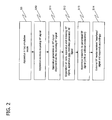
Figure 2 is a flow diagram describing the operation of the apparatus of the present invention in tag emulation mode. -
Figure 3 is a circuit diagram of elements, used in reader mode, of an apparatus according to a first embodiment of the present invention -
Figure 4 is a circuit diagram of elements, used in tag emulation mode, of an apparatus according to an exemple. -
Figure 5 is a circuit diagram of elements, used in tag emulation mode, of an apparatus according to the present invention. -
Figure 6 is a circuit diagram of functional elements of the phase lock loop shown inFigure 5 . -
Figure 7 is a circuit diagram of an apparatus as used within a larger device. -
Figure 8 is a flow diagram describing the mode of operation of an apparatus within a larger device. - The apparatus of the present invention may be used either itself as a reader and tag emulation apparatus, whether in hand-held form or other form or alternatively it may form part of a larger device, such as a consumer electronic device, mobile telephone or personal digital assistant. When forming part of a larger device, such apparatus may be included as a discrete unit, be integrated within the electronic circuitry of the larger device or alternatively use parts of the electronic circuitry and parts within the larger device.
- The apparatus of the present invention operates in two modes, referred to herein as 'reader' mode and 'tag emulation' mode. The apparatus will be referred to herein as a dual mode apparatus, although it should be understood that more than two modes may be provided. The dual mode apparatus may be set up to operate in either mode as default. The change in mode of operation may be due to operation of the larger device, receipt of an externally generated RF signal by the dual mode apparatus or as a result of some instruction received from within the dual mode. Preferably the dual mode apparatus will be set to operate in 'tag emulation' mode as default as this has the advantage of saving power within the apparatus or larger device. In one embodiment the dual mode apparatus may automatically switch to 'reader' mode at certain time intervals or on receipt of a signal, for example from the larger device. The switch may also occur as the result of the detection of an externally generated RF field, for example by an active tag system. As an alternative, the dual mode apparatus could operate as a default in reader mode but transmit its RF signals at predefined intervals rather than continuously. The switch to tag emulation mode may then occur on detection of an externally generated RF signal, for example from another RF reader device.
-
Figure 1 shows a flow diagram of one embodiment of the operation of the apparatus in reader mode. At S 1 the apparatus is in reader mode. As such it will be transmitting an RF carrier signal. This signal may or may not be modulated (S2). The modulation will be effected by the apparatus in reader mode according to data and/or commands to which it has access (either within the apparatus itself or within the larger device). Should there be a data supply device (tag or second dual mode apparatus in tag emulation mode) within the range of the transmitted RF signal, the transmitted RF signal together with any modulated carrier signal will be received by the data supply device (S3). The data supply device will then demodulate the incoming carrier signal, thereby reading the data and/or commands. As a result of the received data and/or commands, the data supply device will modulate the carrier signal supplied by the apparatus in accordance with the data in or available to such data supply device (S4). The apparatus will then receive such modulated carrier signal (S6) and demodulate the carrier signal to obtain the data (S7). Depending on the data obtained, activity or functionality or operation of the apparatus or larger device will be accordingly affected (S8). -
Figure 2 shows a flow diagram of one embodiment of the operation of the apparatus in tag emulation mode. At S9 the apparatus is in tag emulation mode. The apparatus of the invention will receive an incoming, externally generated RF signal when it comes into the range of such a signal (S10). Such RF signal may be generated by a second apparatus of the present invention or alternatively a standard RF reader. Such signal may or may not comprise a modulated carrier signal. On receipt of the incoming RF signal the apparatus will generate its own RF signal dependent on the characteristics of the incoming RF signal (S11). The generation means is preferably sensitive to the phase of the incoming RF signal. Such phase sensitivity can be achieved by the use of a phase lock loop mechanism, described in more detail below, or other phase coherent detection or phase sensitive detection systems. Such generation could also include digital generation means. Dependent on the data and/or commands available to the apparatus and dependent on the incoming RF signal the apparatus may then modulate the internally generated RF signal (S12). The apparatus will then transmit the generated RF signal (S13). Transmission may occur once the correct internal RF signal has been generated. Alternatively such transmission may occur at a particular time, for example dependent on various standard protocols. The transmitted RF signal will interfere with the incoming RF signal. It is this interference which the external reader or second apparatus will receive (S14) and its response will follow that of a standard RF reader response (see for exampleFigure 1 ). -
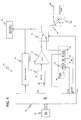
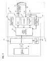
Figures 3 and4 are circuit diagrams showing elements of the apparatus used in reader and tag emulation modes, respectively. Some elements, referenced with a reference numeral which is unique to one ofFigures 3 and4 , are used in only one of the modes. Other elements, which are referenced with the same reference numerals in bothFigures 3 and4 , are used in each mode; it should be understood that, whilst the re-use of components in both modes is preferable, in alternative embodiments of the invention, such shared elements may be replaced by separate components which are each used in only one mode.Figure 3 is a circuit diagram of the apparatus according to a first embodiment of the present invention in reader mode. The elements used inreader mode 100 include amicro-controller 132, amodulator function 102, adriver function 104, anantenna 122, a data receiver anddemodulator 148. - A data supply device 126 (for example an RF tag or second dual mode apparatus of the present invention) interacts with the
apparatus 100 by employing available radio-frequency signals used in RFID applications and NFC systems. For example in this embodiment RF signals at 13.56 MHz are used to communicate between the apparatus and data supply device. - The dual mode apparatus in reader mode is arranged to have generating means 150 for generating an RF carrier signal. The apparatus uses a
modulator 102 to modulate the generated carrier signal, if required, in accordance with the data and/or commands available to it, for example from themicroprocessor 132. The carrier signal (whether modulated or not) is then transmitted viaantenna 144. Following transmission the modulated carrier signal is received by adata supply device 126 byantenna 144 and demodulated by such data storage device. Preferably such communication between the dual mode apparatus and data supply device will be through inductive coupling means. Dependent on such demodulated signal and the data and/or commands available to the data storage device, thedata supply device 126 is arranged to modulate the incoming carrier signal in accordance with such data and/or commands. On receipt of such modulated carrier signal by the dual mode apparatus, theapparatus 100 is arranged to havemeans 148 to demodulate such carrier signal and read data or commands supplied by data storage device. -
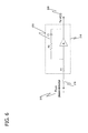
Figure 4 is a circuit diagram of elements of the apparatus used in tag emulation mode, according to an example.
Theapparatus 100 includes amicro-controller 132, amodulator function 102, adriver function 104, anantenna 122 and a phase-lockedloop 149 comprising in this embodiment a voltage controlled oscillator (VCO) 108, aphase detector 110, aloop filter 112 and preferably a sample and holdcircuit 114. Although shown separately inFigures 3 and4 , the modulator anddriver functions switch 128, which indirectly controls the operational mode (i.e. whether reader or tag emulation) through coupling of incoming RF signal to phase lock loop mechanism and means 106 for controlling the modulation or RF signal output level. The apparatus will also have access to, whether within itself (for example as part of the microcontroller) or as part of a separate component or larger device, adata store 134. - The dual mode apparatus operates with a power supply (not represented). Such power supply may be specific to the apparatus itself, it may be dependent on the mode of operation or the apparatus may use a pre-existing power supply within a larger device. For example when in tag emulation mode, the apparatus may derive power from its own internal power supply, from the power supply in a larger device of which it is a part or from an externally generated RF field or signal.
- A reader device 146 (for example an RF reader or second dual mode apparatus of the present invention) interacts with the
apparatus 100 by employing available radio-frequency signals used in RFID applications and NFC systems. For example in this embodiment RF signals at 13.56 MHz are used to communicate reader to tag or tag emulator. - In tag emulation mode, the apparatus receives an RF signal from an
external reader device 146, or second dual mode apparatus. Such RF signal will be received when the apparatus is within range of theexternal reader device 146. In a preferred embodiment tag emulation mode is the default mode. Where the default mode is not tag emulation or where the apparatus is in reader mode then the apparatus has means to switch from reader mode into tag emulation mode. Such means might comprise aswitch 128. Such means might operate on direction from themicroprocessor 132 either as a result of RF signal detection, a return to default mode or a signal supplied from larger device. Alternatively the apparatus can be set up to automatically convert into tag emulation mode on receipt of an RF signal by theantenna 122. - Where a
switch 128 is present, the switch is set to connect theantenna 122 with the phase-lockedloop 149 of thedual mode apparatus 100. Once in tag emulation mode theVCO 108 will continuously generate an internal RF signal. The phase-lockedloop 149, which is preferably a second order loop, comprises means by which the internally generated RF signal is brought into phase with the received (externally generated) RF signal. In a preferred embodiment, theVCO 108 is connected to thephase detector 110 via aloop filter 112 and a sample and holdcircuit 114. Thephase detector 110 detects the difference in frequency and phase between the VCO generated RF signal and the received RF signal. A signal is then sent from the phase detector to the loop filter resulting in an adjustment to the voltage generated by such loop filter. This in turn adjusts the phase and frequency of signal generated by the VCO. This process is continuously repeated to ensure the VCO signal and external RF signal match. - The phase lock loop process will continue until an instruction to modulate and transmit the internally generated RF signal is received from the microprocessor. This may occur once phase locking between the external RF signal and VCO generated signal has been detected by
microprocessor 132. Alternatively, this may occur once the apparatus is ready to transmit and modulate, for example at a time interval prescribed by operating protocols such as ISO 14443. - Where the apparatus includes a sample and hold
circuit 114 this will be enabled at the same time as the phase lock loop ceases to operate. - The
apparatus 100 is then arranged to modulate and transmit the VCO generated RF signal similar to the manner in which the carrier signal is transmitted by the apparatus in reader mode as described above, and the relevant description thereof above should be understood to apply. - Different types of modulation or interference or combinations of modulation/interference are possible for the transmission of the VCO generated RF signal, e.g. in-phase only causing constructive interference, out-of phase only causing destructive interference, a combination of in- and out-of phase, partially in- and/or out- of phase or a combination of partially in- and/or out- of phase.
- In one alternative example, the apparatus includes a
modulation controller 106. Themodulation controller 106 controls the amplitude of the modulated carrier signal or modulated VCO generated signal in accordance with either the proximity of the external reader device, and/or the characteristic of the received RF signal or and/or the proximity of the data storage device. Where the modulation controller uses detection of external signal strength this can be implemented by providing an amplitude levelling loop having a signal strength detector block (similar to that shown inFigure 5 as element 230) which captures a sampled measurement of the incoming RF signal strength. The strength information can be used, within themicro-controller 132 andmodulation controller 106, in conjunction with other calibration or predictive data if required, to set and control the modulation depth, with themodulator 102 and thedriver 104, to a desired value using for example a modulation controlled algorithm. This desired value could be a constant, or varying, modulation depth of between, for example, 10% and 100%. - In
Figure 4 , the modulated VCO generatedsignal 142 on transmission is set to cause destructive or constructive interference or a combination of both with the received RF signal on transmission fromantenna 122 to theexternal reader device 146 via theantenna 144. - Once transmission is completed by the apparatus in reader mode, the apparatus mode can be toggled back into tag emulation mode, for example through the
switch 128. -
Figure 5 is a circuit diagram of elements used in tag emulation mode in dual mode apparatus according to the present invention. The reference numbers of similar components toFigure 4 have been incremented by 100, and the relevant description of those components above should be taken to apply. Further, although not illustrated, elements used during operation of the device in reader mode will be similar to those illustrated inFigure 3 above, and the relevant description of those components above should be taken to apply. - As described above, operation of the apparatus will depend on whether the apparatus is in reader or tag emulation mode. In addition to the first embodiment, apparatus of the second embodiment additionally includes a
clamp 220 and a composite loop filter and holdfunction 218. The composite loop filter and holdfunction 218 replaces the loop filter and sample & hold components inFigure 4 of the previous embodiment. - The
clamp 220 is used to reduce the risk of high voltages destroying chip functionality. In circumstances where high voltages might or do occur, for example when the apparatus is in the field of another RF reader device, current is diverted through the clamp thereby preventing high voltages from affecting the chip functionality. - The composite loop filter and hold
function 218 is detailed further inFigure 6 . - When activated the
VCO 208 continuously generates an internal RF signal. Likewise thephase detector 210, whilst active, continually detects the phase difference between the internally generated signal and any external RF signal and signals the loop filter to increase voltage. In the first embodiment, when the apparatus switches back to reader mode to modulate and transmit the internally generated signal, the phase detector and loop filter continue to operate. This continued operation results in a slow recovery once a new external RF signal is received and the apparatus is operating again in tag emulation mode. In this embodiment, the composite loop and function is placed into hold mode by opening aswitch 216 ofFigure 6 . When open, the filter can be approximated as a floating integrator whose capacitive element C1, referenced 250, will hold its state as per the last signal received from the phase detector, neglecting any further signals sent by the phase detector. This function can be better described as a "filter and hold function". The filter may be commanded into hold mode only when the phase lock loop has completely stabilized and the output of thephase detector 210 is no longer changing. Alternatively the command can be linked to the modulation and transmission of the VCO signal, for example as required under various communication protocols or as determine by the microprocessor. -
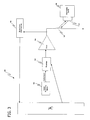
Figure 7 is a circuit diagram of an RFID apparatus in accordance with an embodiment of the invention, as used within a larger device. - The
larger device 376 may, for example, be a mobile telephone terminal. The apparatus may be integrated into such larger device either as a stand-alone unit in similar form to that described above or in such a way that pre-existing mobile telephone components are used and duplication of function avoided, or alternatively as a silicon block within the main device body. Integrating the apparatus of the present invention into such a larger device would allow such a device to operate both as an RF reader and as a tag in the vicinity of other RF reader. Where thelarger device 376 is a mobile telephone, when the apparatus is operating in reader mode, the mobile telephone could be used to read tags within objects such as posters and, for example download information or sound tracks from such posters. When operating in tag emulation mode, the mobile telephone could act as an authorisation means such as a train ticket. The mobile telephone would be 'read' by an RF reader, such as a station entrance gate and bring about operation of the entrance gate. - Other examples of the larger device could be a personal computer device or personal digital assistant (PDA) again acting in reader mode to read external RF tags and in tag mode when in range of a second RF reader (for example a station entrance gate), vending machines in which reader and tag emulation are required (for example operating in reader mode when a user wishes to buy an item from the vending machine and tag mode when the owner of the vending machine wishes to download purchasing data), watches acting in similar fashion to mobile telephone terminals or personal computer devices, hand held identification devices and electronic tickets (this would enable the user to both have an identification source in tag emulation mode and reading ability when in reader mode), access and entry systems (in which reader mode is used to read entry by, for example visitors, and then tag emulation mode when download of access information and data is required), medical and diagnostic systems (for example patient identification wristbands in which reader mode is used to read RF tags on drug vials or medication systems and tag emulation mode is used to provide an audit trail and to identify the patient).
- In
Figure 7 the RFID apparatus is represented withindotted block 370. It is assumed in this embodiment that the required processing power for theapparatus 370 will be provided by either a host processor or independent processor. Alternatively, the apparatus may have its own microprocessor as previously described. InFigure 7 , the microprocessor within the apparatus is therefore replaced by what is referred to as the "reader, encoder & decoder tag controller" (or simply "controller" below) 322 and represents those parts of the apparatus architecture which can not be found within the pre-existing larger device system. For example the controller may control the timing of operations conducted in theRFID apparatus 370, for example the time of modulation or demodulation (for example because the larger device processor is engaged elsewhere), routing of signals (for example from theTag emulator PLL 354 to the Driver 304), modulation of both internally generated VCO signal and RF carrier signal (alternatively modulation may occur within the driver 304), switch function for phase lock loop functionality (corresponding toelement 216 inFigure 6 ). The signal detection and modulationdepth control part 356 detects the characteristics of an incoming RF signal and provides a signal to thecontroller 322 which then performs the function of the modulation controller (corresponding toelement 106 inFigure 4 andelement 206 onFigure 5 ) either itself or through the host processor or independent processor. The tag emulator phase lock loop (PLL) 354 provides the generating means for tag emulation. The internally VCO generated RF signal produced by the phase lock loop feeds in to the controller for modulation and onwards transmission. Thedemodulator 352 takes any incoming externally generated RF signal and demodulates such signal to obtain data and/or commands. Thedriver 304 and signal generating means 358 perform the same functions as previously described (corresponding toelements Figure 3 ). The RFID apparatus operates in similar fashion to the embodiments described above. - The RFID apparatus interfaces to the larger device through an
interface 362. The interface translates the signals sent between the apparatus and host device so that both parts of the overall system can inter-operate. This interface may form part of the apparatus or be a separate component within the larger host device. Theconfiguration store 364 operates to allow setting of certain parameters or protocols within the apparatus. The configuration store can operate through theinterface 362. Alternatively it may be connected directly to the various component parts of the apparatus and act directly on such component parts. Further it may also form part of the host device processor, in which case interpretation/action will occur through thecontroller 322. - In
Figure 7 the processing capability is either provided through the pre-existing host processor or through an independent microprocessor. -
Figure 8 is a flow diagram describing an example of the operation of the device illustrated inFigure 7 . - The RFID apparatus of the mobile telephone terminal is initially set in a default mode, step S16, in this case tag emulation mode, i.e. no RF signal is being transmitted. It is first determined if a user input is detected, step S17. This may be as a result of the mobile telephone user selecting RF reading capability by button selection on the main body of the mobile telephone device, for example they wish to 'read' a data supply device on a poster. Should such occur then the telephone microprocessor will signal the apparatus and the apparatus will switch to operation in reader mode (S21). The apparatus will then operate in a reader mode for the duration required or for a set time period, step S21. At conclusion of duration required (for example user turns reader function off) or reading time expires, the apparatus reverts to tag emulation mode (S16). If there is no mobile telephone user input detected, the apparatus continues to operate in tag emulation mode until a suitable RF signal is detected. If a carrier signal is detected, corresponding for example to the case where the mobile acts as a train ticket and the station entrance gate includes an RF reader, the apparatus operates as a tag and responds to the received RF signal according to its available data and/or command set.
- The above embodiments are to be understood as illustrative examples of the invention. Further embodiments of the invention are envisaged. For example, the proposed solution may also be used with other forms of antenna, and other coupling mechanisms, such as far field electromagnetic, acoustic or optical. Other examples of phase coherent detection or phase sensitive detection systems would include but are not limited to injection locking receiving circuitry, parametric amplifying receiving circuitry and delay lock loop receiving circuitry. Applications in other electronic devices other than mobile telephones are also envisaged, such as PDAs, laptops, game consoles, electronic wallets or purses, vending machines, watches, identity (ID) devices, electronic ticket devices, access and entry systems, patient identification devices or medical devices.
- It is to be understood that any feature described in relation to any one embodiment may be used alone, or in combination with other features described, and may also be used in combination with one or more features of any other of the embodiments, or any combination of any other of the embodiments. Furthermore, equivalents and modifications not described above may also be employed without departing from the scope of the invention, which is defined in the accompanying claims.
Claims (8)
- RFID apparatus configured to operate in a reader mode and a tag emulation mode, comprising:for operating said RFiD apparatus in said reader mode:transmission means for transmitting an RF signal;reception means for receiving a modulated RF signal; anddemodulation means (148, 248, 352) for demodulating a received modulatedsignal, and for operating said RFiD apparatus in said tag emulation mode:generating means (149, 354) for generating a RF signal dependent on an incoming RF signal, said incoming RF signal being generated by different apparatus, wherein the apparatus is arranged to transmit said generated RF signal via said transmission means such that said generated RF signal interferes with the incoming RF signal, andwherein said transmission means and said reception means comprise a single antenna (122, 222, 323), characterised in thatsaid generating means comprises phase sensitive means responsive to phase in said incoming RF signal, said phase sensitive means comprising a phase locked loop,wherein said phase locked loop comprises:a phase detector (210) adapted to receive said incoming RF signal;a switch (216) coupled to said phase detector;a composite loop filter and hold function circuit (218) coupled to said switch; anda voltage-controlled oscillator, VCO, (208), coupled to said composite loop filter and hold function circuit, said VCO adapted to generate said RF signal dependent on said incoming RF signal and said phase detector adapted to receive said generated RF signal, andwherein said switch is adapted to close upon receiving said incoming RF signal and open when said incoming RF signal matches said generated RF signal.
- RFID apparatus according to claim 1, wherein the phase locked loop is a second order loop.
- RFID apparatus according to any preceding claim, wherein said apparatus further comprises a modulator (202), said modulator adapted to modulate said generated RF signal prior to transmission of said generated RF signal.
- RFID apparatus according to claim 3, wherein said apparatus further comprises a modulation-controller (206) adapted to control said modulator based upon a signal strength of said incoming RF signal.
- RFID apparatus according to any preceding claim, wherein the apparatus is arranged such that:during said reader mode, the apparatus can transmit an RF signal to a first external device and can receive a modulated RF signal from said first external device; andduring said tag emulation mode, the apparatus can generate an RF signal dependent upon an incoming RF signal received from a second external device, and transmit said generated RF signal to said second external device.
- RFID apparatus according to claim 5, wherein the reader and/or tag emulation mode of operation is independently selectable.
- RFID apparatus according to claim 6, wherein the mode of operation is selected in dependence on detection of an externally generated RF signal.
- An electrical device (376) incorporating an RFID apparatus according to any preceding claim.
Applications Claiming Priority (3)
| Application Number | Priority Date | Filing Date | Title |
|---|---|---|---|
| GB0325249A GB0325249D0 (en) | 2003-10-29 | 2003-10-29 | Dual mode reader/tag architecture |
| GB0405026A GB0405026D0 (en) | 2004-03-05 | 2004-03-05 | Dual mode reader/tag architecture |
| PCT/GB2004/004572 WO2005045744A1 (en) | 2003-10-29 | 2004-10-29 | Rfid apparatus |
Publications (2)
| Publication Number | Publication Date |
|---|---|
| EP1761880A1 EP1761880A1 (en) | 2007-03-14 |
| EP1761880B1 true EP1761880B1 (en) | 2013-02-27 |
Family
ID=33518441
Family Applications (1)
| Application Number | Title | Priority Date | Filing Date |
|---|---|---|---|
| EP04791609A Active EP1761880B1 (en) | 2003-10-29 | 2004-10-29 | Rfid apparatus |
Country Status (4)
| Country | Link |
|---|---|
| US (2) | US8373544B2 (en) |
| EP (1) | EP1761880B1 (en) |
| GB (1) | GB2406023B (en) |
| WO (1) | WO2005045744A1 (en) |
Families Citing this family (115)
| Publication number | Priority date | Publication date | Assignee | Title |
|---|---|---|---|---|
| AU2003303597A1 (en) | 2002-12-31 | 2004-07-29 | Therasense, Inc. | Continuous glucose monitoring system and methods of use |
| US7587287B2 (en) * | 2003-04-04 | 2009-09-08 | Abbott Diabetes Care Inc. | Method and system for transferring analyte test data |
| US7679407B2 (en) * | 2003-04-28 | 2010-03-16 | Abbott Diabetes Care Inc. | Method and apparatus for providing peak detection circuitry for data communication systems |
| US8127984B2 (en) * | 2003-06-13 | 2012-03-06 | Varia Holdings Llc | Emulated radio frequency identification |
| EP1761880B1 (en) | 2003-10-29 | 2013-02-27 | Innovision Research & Technology PLC | Rfid apparatus |
| EP1718198A4 (en) * | 2004-02-17 | 2008-06-04 | Therasense Inc | Method and system for providing data communication in continuous glucose monitoring and management system |
| CA2858901C (en) | 2004-06-04 | 2024-01-16 | Carolyn Anderson | Diabetes care host-client architecture and data management system |
| DE102004031092A1 (en) | 2004-06-28 | 2006-01-12 | Giesecke & Devrient Gmbh | transponder unit |
| US8029441B2 (en) | 2006-02-28 | 2011-10-04 | Abbott Diabetes Care Inc. | Analyte sensor transmitter unit configuration for a data monitoring and management system |
| US7545272B2 (en) | 2005-02-08 | 2009-06-09 | Therasense, Inc. | RF tag on test strips, test strip vials and boxes |
| US8249500B2 (en) | 2005-02-24 | 2012-08-21 | Innovision Research & Technology Plc | Tuneable NFC device |
| US7768408B2 (en) | 2005-05-17 | 2010-08-03 | Abbott Diabetes Care Inc. | Method and system for providing data management in data monitoring system |
| WO2006134428A1 (en) | 2005-06-14 | 2006-12-21 | Nokia Corporation | Tag multiplication |
| FR2890207B1 (en) * | 2005-08-23 | 2007-11-02 | Inside Contactless Sa | INDUCTIVE COUPLING READER COMPRISING MEANS FOR EXTRACTING AN ELECTRIC POWER SUPPLY VOLTAGE |
| EP1921980A4 (en) | 2005-08-31 | 2010-03-10 | Univ Virginia | Improving the accuracy of continuous glucose sensors |
| US7756561B2 (en) * | 2005-09-30 | 2010-07-13 | Abbott Diabetes Care Inc. | Method and apparatus for providing rechargeable power in data monitoring and management systems |
| US7583190B2 (en) * | 2005-10-31 | 2009-09-01 | Abbott Diabetes Care Inc. | Method and apparatus for providing data communication in data monitoring and management systems |
| US8985436B2 (en) | 2006-01-18 | 2015-03-24 | Symbol Technologies, Inc. | Peer-to-peer radio frequency communications for management of RFID readers |
| US7620438B2 (en) | 2006-03-31 | 2009-11-17 | Abbott Diabetes Care Inc. | Method and system for powering an electronic device |
| US9392969B2 (en) | 2008-08-31 | 2016-07-19 | Abbott Diabetes Care Inc. | Closed loop control and signal attenuation detection |
| US8478557B2 (en) | 2009-07-31 | 2013-07-02 | Abbott Diabetes Care Inc. | Method and apparatus for providing analyte monitoring system calibration accuracy |
| US8219173B2 (en) | 2008-09-30 | 2012-07-10 | Abbott Diabetes Care Inc. | Optimizing analyte sensor calibration |
| US7801582B2 (en) | 2006-03-31 | 2010-09-21 | Abbott Diabetes Care Inc. | Analyte monitoring and management system and methods therefor |
| ES2676623T3 (en) * | 2006-04-24 | 2018-07-23 | Nokia Technologies Oy | System and method for managing and controlling near-field communication for a mobile multifunctional device when the device is not charged or is only partially charged |
| US8081060B1 (en) | 2006-05-12 | 2011-12-20 | Nokia Corporation | System and method for communications establishment |
| WO2007139969A2 (en) * | 2006-05-26 | 2007-12-06 | Symbol Technologies, Inc. | Data format for efficient encoding and access of multiple data items in rfid tags |
| US20090105571A1 (en) * | 2006-06-30 | 2009-04-23 | Abbott Diabetes Care, Inc. | Method and System for Providing Data Communication in Data Management Systems |
| CN100370470C (en) * | 2006-07-10 | 2008-02-20 | 胡淼龙 | Ultra-long distance microwave electronic marking system |
| FR2905782B1 (en) * | 2006-09-11 | 2008-12-05 | Inside Contactless Sa | METHOD FOR CONNECTING A NON-CONTACT INTEGRATED CIRCUIT TO AN NFC COMPONENT |
| US20080199894A1 (en) | 2007-02-15 | 2008-08-21 | Abbott Diabetes Care, Inc. | Device and method for automatic data acquisition and/or detection |
| US8123686B2 (en) | 2007-03-01 | 2012-02-28 | Abbott Diabetes Care Inc. | Method and apparatus for providing rolling data in communication systems |
| CA2683930A1 (en) | 2007-04-14 | 2008-10-23 | Abbott Diabetes Care Inc. | Method and apparatus for providing data processing and control in medical communication system |
| WO2008130897A2 (en) * | 2007-04-14 | 2008-10-30 | Abbott Diabetes Care, Inc. | Method and apparatus for providing data processing and control in medical communication system |
| WO2008130898A1 (en) | 2007-04-14 | 2008-10-30 | Abbott Diabetes Care, Inc. | Method and apparatus for providing data processing and control in medical communication system |
| WO2009096992A1 (en) | 2007-04-14 | 2009-08-06 | Abbott Diabetes Care, Inc. | Method and apparatus for providing data processing and control in medical communication system |
| WO2008130896A1 (en) | 2007-04-14 | 2008-10-30 | Abbott Diabetes Care, Inc. | Method and apparatus for providing data processing and control in medical communication system |
| US20080278332A1 (en) * | 2007-05-08 | 2008-11-13 | Abbott Diabetes Care, Inc. | Analyte monitoring system and methods |
| US7928850B2 (en) | 2007-05-08 | 2011-04-19 | Abbott Diabetes Care Inc. | Analyte monitoring system and methods |
| US20080281179A1 (en) * | 2007-05-08 | 2008-11-13 | Abbott Diabetes Care, Inc. | Analyte monitoring system and methods |
| US8461985B2 (en) | 2007-05-08 | 2013-06-11 | Abbott Diabetes Care Inc. | Analyte monitoring system and methods |
| US20080281171A1 (en) * | 2007-05-08 | 2008-11-13 | Abbott Diabetes Care, Inc. | Analyte monitoring system and methods |
| US8665091B2 (en) | 2007-05-08 | 2014-03-04 | Abbott Diabetes Care Inc. | Method and device for determining elapsed sensor life |
| US8456301B2 (en) | 2007-05-08 | 2013-06-04 | Abbott Diabetes Care Inc. | Analyte monitoring system and methods |
| US8239166B2 (en) | 2007-05-14 | 2012-08-07 | Abbott Diabetes Care Inc. | Method and apparatus for providing data processing and control in a medical communication system |
| US8260558B2 (en) | 2007-05-14 | 2012-09-04 | Abbott Diabetes Care Inc. | Method and apparatus for providing data processing and control in a medical communication system |
| US8560038B2 (en) | 2007-05-14 | 2013-10-15 | Abbott Diabetes Care Inc. | Method and apparatus for providing data processing and control in a medical communication system |
| US8444560B2 (en) | 2007-05-14 | 2013-05-21 | Abbott Diabetes Care Inc. | Method and apparatus for providing data processing and control in a medical communication system |
| US9125548B2 (en) | 2007-05-14 | 2015-09-08 | Abbott Diabetes Care Inc. | Method and apparatus for providing data processing and control in a medical communication system |
| US8600681B2 (en) * | 2007-05-14 | 2013-12-03 | Abbott Diabetes Care Inc. | Method and apparatus for providing data processing and control in a medical communication system |
| US10002233B2 (en) * | 2007-05-14 | 2018-06-19 | Abbott Diabetes Care Inc. | Method and apparatus for providing data processing and control in a medical communication system |
| US8103471B2 (en) | 2007-05-14 | 2012-01-24 | Abbott Diabetes Care Inc. | Method and apparatus for providing data processing and control in a medical communication system |
| TWI500609B (en) * | 2007-06-12 | 2015-09-21 | Solvay | Product containing epichlorohydrin, its preparation and its use in various applications |
| AU2008265542B2 (en) | 2007-06-21 | 2014-07-24 | Abbott Diabetes Care Inc. | Health monitor |
| US8597188B2 (en) | 2007-06-21 | 2013-12-03 | Abbott Diabetes Care Inc. | Health management devices and methods |
| WO2008157819A1 (en) * | 2007-06-21 | 2008-12-24 | Abbott Diabetes Care, Inc. | Health management devices and methods |
| US8160900B2 (en) | 2007-06-29 | 2012-04-17 | Abbott Diabetes Care Inc. | Analyte monitoring and management device and method to analyze the frequency of user interaction with the device |
| US9727812B2 (en) * | 2007-07-23 | 2017-08-08 | Avery Dennison Retail Information Services, Llc | RFID device wtih control logic, and method |
| US20090036760A1 (en) * | 2007-07-31 | 2009-02-05 | Abbott Diabetes Care, Inc. | Method and apparatus for providing data processing and control in a medical communication system |
| US8834366B2 (en) | 2007-07-31 | 2014-09-16 | Abbott Diabetes Care Inc. | Method and apparatus for providing analyte sensor calibration |
| ES2293856B1 (en) * | 2007-08-28 | 2009-04-01 | Pedro Zalbide Elustondo | DISPENSING MACHINE WITH ANTENNA. |
| WO2009039871A1 (en) * | 2007-09-24 | 2009-04-02 | Siemens Aktiengesellschaft | Data synchronization of rfid tags |
| JP5125465B2 (en) * | 2007-12-11 | 2013-01-23 | ソニー株式会社 | Communication device |
| US20090164239A1 (en) | 2007-12-19 | 2009-06-25 | Abbott Diabetes Care, Inc. | Dynamic Display Of Glucose Information |
| US7701348B2 (en) * | 2008-01-18 | 2010-04-20 | International Business Machines Corporation | Embedded system architecture for RFID tag emulation |
| JP5315849B2 (en) * | 2008-01-22 | 2013-10-16 | 株式会社リコー | COMMUNICATION DEVICE, COMMUNICATION METHOD, COMMUNICATION PROGRAM |
| JP2009176027A (en) * | 2008-01-24 | 2009-08-06 | Toshiba Corp | Radio communication device and radio communication system |
| US20090221232A1 (en) * | 2008-02-29 | 2009-09-03 | Estevez Leonardo W | Portable Telephone With Unitary Transceiver Having Cellular and RFID Functionality |
| US7826382B2 (en) | 2008-05-30 | 2010-11-02 | Abbott Diabetes Care Inc. | Close proximity communication device and methods |
| EP2177922A1 (en) * | 2008-10-15 | 2010-04-21 | Gemalto SA | Method for testing an electronic identity document and corresponding device |
| US9402544B2 (en) | 2009-02-03 | 2016-08-02 | Abbott Diabetes Care Inc. | Analyte sensor and apparatus for insertion of the sensor |
| WO2010127050A1 (en) | 2009-04-28 | 2010-11-04 | Abbott Diabetes Care Inc. | Error detection in critical repeating data in a wireless sensor system |
| EP2424426B1 (en) | 2009-04-29 | 2020-01-08 | Abbott Diabetes Care, Inc. | Method and system for providing data communication in continuous glucose monitoring and management system |
| WO2010138856A1 (en) | 2009-05-29 | 2010-12-02 | Abbott Diabetes Care Inc. | Medical device antenna systems having external antenna configurations |
| US8993331B2 (en) | 2009-08-31 | 2015-03-31 | Abbott Diabetes Care Inc. | Analyte monitoring system and methods for managing power and noise |
| BR112012000220A2 (en) | 2009-08-31 | 2020-12-22 | Abbott Diabetes Care Inc. | METHODS AND MEDICAL DEVICES |
| US9314195B2 (en) | 2009-08-31 | 2016-04-19 | Abbott Diabetes Care Inc. | Analyte signal processing device and methods |
| WO2011041531A1 (en) | 2009-09-30 | 2011-04-07 | Abbott Diabetes Care Inc. | Interconnect for on-body analyte monitoring device |
| US8786440B2 (en) * | 2009-10-02 | 2014-07-22 | Checkpoint Systems, Inc. | Calibration of beamforming nodes in a configurable monitoring device system |
| EP2558970A4 (en) * | 2010-01-22 | 2013-11-06 | Abbott Diabetes Care Inc | Method, device and system for providing analyte sensor calibration |
| WO2011112753A1 (en) | 2010-03-10 | 2011-09-15 | Abbott Diabetes Care Inc. | Systems, devices and methods for managing glucose levels |
| US8635046B2 (en) | 2010-06-23 | 2014-01-21 | Abbott Diabetes Care Inc. | Method and system for evaluating analyte sensor response characteristics |
| CN103201751A (en) * | 2010-09-13 | 2013-07-10 | 特里登特Rfid私人有限公司 | System and method for updating parameters and firmware on RFID readers |
| FR2965082B1 (en) * | 2010-09-21 | 2012-09-28 | Inside Contactless | METHOD AND DEVICE FOR INDUCTIVE COUPLING ACTIVATED LOAD MODULATION |
| EP2624745A4 (en) | 2010-10-07 | 2018-05-23 | Abbott Diabetes Care, Inc. | Analyte monitoring devices and methods |
| US10136845B2 (en) | 2011-02-28 | 2018-11-27 | Abbott Diabetes Care Inc. | Devices, systems, and methods associated with analyte monitoring devices and devices incorporating the same |
| EP3583901A3 (en) | 2011-02-28 | 2020-01-15 | Abbott Diabetes Care, Inc. | Devices, systems, and methods associated with analyte monitoring devices and devices incorporating the same |
| US9384373B2 (en) | 2011-10-26 | 2016-07-05 | Qualcomm Incorporated | Adaptive signal scaling in NFC transceivers |
| US9069536B2 (en) | 2011-10-31 | 2015-06-30 | Abbott Diabetes Care Inc. | Electronic devices having integrated reset systems and methods thereof |
| WO2013066849A1 (en) | 2011-10-31 | 2013-05-10 | Abbott Diabetes Care Inc. | Model based variable risk false glucose threshold alarm prevention mechanism |
| EP2775918B1 (en) | 2011-11-07 | 2020-02-12 | Abbott Diabetes Care Inc. | Analyte monitoring device and methods |
| FR2982686B1 (en) * | 2011-11-10 | 2013-11-29 | St Microelectronics Rousset | PROTECTION OF A RADIO FREQUENCY EMISSION-RECEPTION TERMINAL AGAINST ELECTROMAGNETIC DISTURBANCES |
| US8710993B2 (en) | 2011-11-23 | 2014-04-29 | Abbott Diabetes Care Inc. | Mitigating single point failure of devices in an analyte monitoring system and methods thereof |
| US9317656B2 (en) | 2011-11-23 | 2016-04-19 | Abbott Diabetes Care Inc. | Compatibility mechanisms for devices in a continuous analyte monitoring system and methods thereof |
| EP2629235B1 (en) * | 2012-02-17 | 2016-04-13 | ams AG | RFID, reader, RFID network and method for communication in an RFID network |
| CN103366213B (en) * | 2012-03-31 | 2016-08-03 | 华矽半导体股份有限公司 | Active electric subtab and method for modulating signal thereof |
| EP2890297B1 (en) | 2012-08-30 | 2018-04-11 | Abbott Diabetes Care, Inc. | Dropout detection in continuous analyte monitoring data during data excursions |
| US9968306B2 (en) | 2012-09-17 | 2018-05-15 | Abbott Diabetes Care Inc. | Methods and apparatuses for providing adverse condition notification with enhanced wireless communication range in analyte monitoring systems |
| KR102048443B1 (en) * | 2012-09-24 | 2020-01-22 | 삼성전자주식회사 | Near field wireless communicating method and apparatus |
| EP2901153A4 (en) | 2012-09-26 | 2016-04-27 | Abbott Diabetes Care Inc | Method and apparatus for improving lag correction during in vivo measurement of analyte concentration with analyte concentration variability and range data |
| US9183419B2 (en) * | 2013-01-02 | 2015-11-10 | The Boeing Company | Passive RFID assisted active RFID tag |
| US10433773B1 (en) | 2013-03-15 | 2019-10-08 | Abbott Diabetes Care Inc. | Noise rejection methods and apparatus for sparsely sampled analyte sensor data |
| US9474475B1 (en) | 2013-03-15 | 2016-10-25 | Abbott Diabetes Care Inc. | Multi-rate analyte sensor data collection with sample rate configurable signal processing |
| WO2014152034A1 (en) | 2013-03-15 | 2014-09-25 | Abbott Diabetes Care Inc. | Sensor fault detection using analyte sensor data pattern comparison |
| US20170185748A1 (en) | 2014-03-30 | 2017-06-29 | Abbott Diabetes Care Inc. | Method and Apparatus for Determining Meal Start and Peak Events in Analyte Monitoring Systems |
| US10447573B2 (en) * | 2014-07-17 | 2019-10-15 | Sysmex Corporation | Method and system for aggregating diagnostic analyzer related information |
| US10061948B2 (en) | 2014-08-25 | 2018-08-28 | Covidien Lp | Systems and methods for emulating RFID transponders of a plurality of medical devices |
| US9727763B2 (en) * | 2014-12-31 | 2017-08-08 | Intermec Ip Corp. | Modulation index (depth) based grouping, addressing, and fingerprinting RFID tags |
| US9461716B2 (en) * | 2015-03-02 | 2016-10-04 | Intel IP Corporation | Near field communications (NFC) modulation feedback apparatus for tuned antenna configurations |
| WO2017011346A1 (en) | 2015-07-10 | 2017-01-19 | Abbott Diabetes Care Inc. | System, device and method of dynamic glucose profile response to physiological parameters |
| WO2018022048A1 (en) * | 2016-07-27 | 2018-02-01 | Hewlett-Packard Development Company, L.P. | Inductive switching |
| WO2018175489A1 (en) | 2017-03-21 | 2018-09-27 | Abbott Diabetes Care Inc. | Methods, devices and system for providing diabetic condition diagnosis and therapy |
| EP3703269B1 (en) * | 2019-02-26 | 2022-06-08 | Nxp B.V. | Phase alignment of a controller clock to a field |
| EP3742341B1 (en) * | 2019-05-20 | 2022-07-27 | Nxp B.V. | Rfid transponder and method of operating the same |
| JP7157256B2 (en) * | 2019-08-02 | 2022-10-19 | アルプスアルパイン株式会社 | Communication system and information terminal |
| TW202303979A (en) * | 2021-02-23 | 2023-01-16 | 麥覺理大學 | Semiconductor devices for radio receivers and transmitters |
Family Cites Families (22)
| Publication number | Priority date | Publication date | Assignee | Title |
|---|---|---|---|---|
| US5003552A (en) * | 1989-11-20 | 1991-03-26 | Unisys Corporation | Carrier aided code tracking loop |
| WO1992008148A1 (en) | 1990-11-06 | 1992-05-14 | Westinghouse Electric Corporation | Dual mode electronic identification system |
| US5604486A (en) * | 1993-05-27 | 1997-02-18 | Motorola, Inc. | RF tagging system with multiple decoding modalities |
| US5841365A (en) * | 1993-09-22 | 1998-11-24 | Seattle Silicon Corporation | Method and apparatus for communicating with a product label |
| DE4410896A1 (en) * | 1994-03-29 | 1995-10-05 | Bosch Gmbh Robert | Vehicle device for transponder operation |
| US5649295A (en) * | 1995-06-19 | 1997-07-15 | Lucent Technologies Inc. | Dual mode modulated backscatter system |
| US5936527A (en) * | 1998-02-10 | 1999-08-10 | E-Tag Systems, Inc. | Method and apparatus for locating and tracking documents and other objects |
| CN1260653A (en) * | 1998-07-24 | 2000-07-19 | 休斯电子公司 | Multi-mode, multi-modulation point-to-multi point communication |
| WO2001041043A1 (en) * | 1999-12-03 | 2001-06-07 | Gemplus Tag (Australia) Pty Ltd | Electronic label reading system |
| GB0102882D0 (en) * | 2001-02-06 | 2001-03-21 | Koninkl Philips Electronics Nv | Signalling system and a transport for use in the system |
| CN100361146C (en) | 2002-03-18 | 2008-01-09 | Nxp股份有限公司 | Portable device comprising a communication station configuration and a data carrier configuration |
| US6892052B2 (en) * | 2002-03-26 | 2005-05-10 | Nokia Corporation | Radio frequency identification (RF-ID) based discovery for short range radio communication |
| US7565108B2 (en) * | 2002-03-26 | 2009-07-21 | Nokia Corporation | Radio frequency identification (RF-ID) based discovery for short range radio communication with reader device having transponder functionality |
| US7274909B2 (en) * | 2002-10-31 | 2007-09-25 | Nokia Corporation | Method and system for selecting data items for service requests |
| US7072672B1 (en) * | 2002-11-01 | 2006-07-04 | Nokia Corporation | Disposable mini-applications |
| WO2004064430A1 (en) * | 2003-01-13 | 2004-07-29 | Telefonaktiebolaget Lm Ericsson (Publ) | Point to multipoint cell plan and migration |
| US6978118B2 (en) * | 2003-02-20 | 2005-12-20 | Nokia Corporation | Apparatus, system, method and computer program product for implementing an automatic identification system with a personal communication device to improve functionality |
| US7446646B2 (en) * | 2003-06-30 | 2008-11-04 | Nokia Corporation | System and method for supporting multiple reader-tag configurations using multi-mode radio frequency tag |
| US7333479B2 (en) * | 2003-06-30 | 2008-02-19 | Nokia Corporation | RFID system with packetized data storage in a mobile environment: methods, systems and program products |
| US7023342B2 (en) * | 2003-09-17 | 2006-04-04 | The United States Of America As Represented By The Secretary Of The Navy | Continuous wave (CW)—fixed multiple frequency triggered, radio frequency identification (RFID) tag and system and method employing same |
| EP1761880B1 (en) | 2003-10-29 | 2013-02-27 | Innovision Research & Technology PLC | Rfid apparatus |
| US7548153B2 (en) * | 2004-07-09 | 2009-06-16 | Tc License Ltd. | Multi-protocol or multi-command RFID system |
-
2004
- 2004-10-29 EP EP04791609A patent/EP1761880B1/en active Active
- 2004-10-29 WO PCT/GB2004/004572 patent/WO2005045744A1/en active Application Filing
- 2004-10-29 US US10/577,504 patent/US8373544B2/en active Active
- 2004-10-29 GB GB0424101A patent/GB2406023B/en active Active
-
2013
- 2013-02-08 US US13/762,976 patent/US9467208B2/en active Active
Also Published As
| Publication number | Publication date |
|---|---|
| GB0424101D0 (en) | 2004-12-01 |
| US20080018433A1 (en) | 2008-01-24 |
| US8373544B2 (en) | 2013-02-12 |
| GB2406023A (en) | 2005-03-16 |
| US20130181818A1 (en) | 2013-07-18 |
| WO2005045744A1 (en) | 2005-05-19 |
| EP1761880A1 (en) | 2007-03-14 |
| US9467208B2 (en) | 2016-10-11 |
| GB2406023A9 (en) | 2005-06-24 |
| GB2406023B (en) | 2005-08-10 |
Similar Documents
| Publication | Publication Date | Title |
|---|---|---|
| EP1761880B1 (en) | Rfid apparatus | |
| US7248834B2 (en) | Communication apparatus | |
| EP1869842B1 (en) | Communications apparatus | |
| KR100862953B1 (en) | Radio frequency identification RF-ID based discovery for short range radio communication with reader device having transponder functionality | |
| US8249502B2 (en) | Radio-frequency communication device, system and method | |
| US6650229B1 (en) | Electromagnetic transponder read terminal operating in very close coupling | |
| EP2076867B1 (en) | Near field rf communicators and near field rf communications enabled devices | |
| EP2284763B1 (en) | Reader/writer and communication method thereof | |
| EP1895449B1 (en) | Data communication system, device for executing ic card function, control method for the device, and information processing terminal | |
| US10650201B1 (en) | RFID tags with port-dependent functionality | |
| WO2008132269A1 (en) | Short range communication | |
| US7979034B2 (en) | Architecture for RFID tag reader/writer | |
| KR20070056974A (en) | A terminal device communicating with contact-less ic media, and a communication method performed in the terminal device | |
| JPH10247863A (en) | Base circuit for contactless calling system including phase-locked voltage-controlled oscillator | |
| WO2005074158A1 (en) | Ic card reading apparatus and reading method thereof | |
| JP2006279813A (en) | Reader/writer | |
| KR20040071137A (en) | A communications unit | |
| JP3743614B2 (en) | Characterizing an electromagnetic transponder system for operation in extreme proximity | |
| Finkenzeller et al. | Range extension of an ISO/IEC 14443 type a RFID system with actively emulating load modulation | |
| AU2014319588A1 (en) | Wireless communication apparatus and portable apparatus | |
| JP2003050977A (en) | Communication system for contactless type ic card, ic card, and ic card reader | |
| US20220368374A1 (en) | Near-field communication device | |
| US20230055356A1 (en) | Electronic device powering | |
| US20230058758A1 (en) | Electronic device powering | |
| EP3945684A1 (en) | Management of the switching of a contactless communication device from a card emulation mode to a peer to peer mode |
Legal Events
| Date | Code | Title | Description |
|---|---|---|---|
| PUAI | Public reference made under article 153(3) epc to a published international application that has entered the european phase |
Free format text: ORIGINAL CODE: 0009012 |
|
| 17P | Request for examination filed |
Effective date: 20060527 |
|
| AK | Designated contracting states |
Kind code of ref document: A1 Designated state(s): DE FR |
|
| RAP1 | Party data changed (applicant data changed or rights of an application transferred) |
Owner name: INNOVISION RESEARCH & TECHNOLOGY PLC |
|
| 17Q | First examination report despatched |
Effective date: 20110114 |
|
| GRAP | Despatch of communication of intention to grant a patent |
Free format text: ORIGINAL CODE: EPIDOSNIGR1 |
|
| GRAS | Grant fee paid |
Free format text: ORIGINAL CODE: EPIDOSNIGR3 |
|
| GRAA | (expected) grant |
Free format text: ORIGINAL CODE: 0009210 |
|
| AK | Designated contracting states |
Kind code of ref document: B1 Designated state(s): DE FR |
|
| REG | Reference to a national code |
Ref country code: DE Ref legal event code: R081 Ref document number: 602004041176 Country of ref document: DE Owner name: BROADCOM EUROPE LTD., CAMBRIDGE, GB Free format text: FORMER OWNER: INNOVISION RESEARCH & TECHNOLOGY PLC, WOKINGHAM, BERKSHIRE, GB |
|
| REG | Reference to a national code |
Ref country code: DE Ref legal event code: R096 Ref document number: 602004041176 Country of ref document: DE Effective date: 20130425 |
|
| PLBE | No opposition filed within time limit |
Free format text: ORIGINAL CODE: 0009261 |
|
| STAA | Information on the status of an ep patent application or granted ep patent |
Free format text: STATUS: NO OPPOSITION FILED WITHIN TIME LIMIT |
|
| PGFP | Annual fee paid to national office [announced via postgrant information from national office to epo] |
Ref country code: FR Payment date: 20131018 Year of fee payment: 10 |
|
| 26N | No opposition filed |
Effective date: 20131128 |
|
| REG | Reference to a national code |
Ref country code: DE Ref legal event code: R097 Ref document number: 602004041176 Country of ref document: DE Effective date: 20131128 |
|
| REG | Reference to a national code |
Ref country code: FR Ref legal event code: ST Effective date: 20150630 |
|
| PG25 | Lapsed in a contracting state [announced via postgrant information from national office to epo] |
Ref country code: FR Free format text: LAPSE BECAUSE OF NON-PAYMENT OF DUE FEES Effective date: 20141031 |
|
| REG | Reference to a national code |
Ref country code: DE Ref legal event code: R082 Ref document number: 602004041176 Country of ref document: DE Representative=s name: BOSCH JEHLE PATENTANWALTSGESELLSCHAFT MBH, DE Ref country code: DE Ref legal event code: R081 Ref document number: 602004041176 Country of ref document: DE Owner name: BROADCOM EUROPE LTD., CAMBRIDGE, GB Free format text: FORMER OWNER: INNOVISION RESEARCH & TECHNOLOGY PLC, CIRENCESTER, GLOUCESTERSHIRE, GB |
|
| PGFP | Annual fee paid to national office [announced via postgrant information from national office to epo] |
Ref country code: DE Payment date: 20220920 Year of fee payment: 19 |