EP1782174B1 - Capacitive sensing apparatus having varying depth sensing elements - Google Patents
Capacitive sensing apparatus having varying depth sensing elements Download PDFInfo
- Publication number
- EP1782174B1 EP1782174B1 EP05764532A EP05764532A EP1782174B1 EP 1782174 B1 EP1782174 B1 EP 1782174B1 EP 05764532 A EP05764532 A EP 05764532A EP 05764532 A EP05764532 A EP 05764532A EP 1782174 B1 EP1782174 B1 EP 1782174B1
- Authority
- EP
- European Patent Office
- Prior art keywords
- sensing element
- sensing
- capacitive
- waveform
- axis
- Prior art date
- Legal status (The legal status is an assumption and is not a legal conclusion. Google has not performed a legal analysis and makes no representation as to the accuracy of the status listed.)
- Not-in-force
Links
Images


Classifications
-
- G—PHYSICS
- G06—COMPUTING; CALCULATING OR COUNTING
- G06F—ELECTRIC DIGITAL DATA PROCESSING
- G06F3/00—Input arrangements for transferring data to be processed into a form capable of being handled by the computer; Output arrangements for transferring data from processing unit to output unit, e.g. interface arrangements
- G06F3/01—Input arrangements or combined input and output arrangements for interaction between user and computer
- G06F3/03—Arrangements for converting the position or the displacement of a member into a coded form
- G06F3/041—Digitisers, e.g. for touch screens or touch pads, characterised by the transducing means
- G06F3/044—Digitisers, e.g. for touch screens or touch pads, characterised by the transducing means by capacitive means
- G06F3/0443—Digitisers, e.g. for touch screens or touch pads, characterised by the transducing means by capacitive means using a single layer of sensing electrodes
-
- G—PHYSICS
- G01—MEASURING; TESTING
- G01R—MEASURING ELECTRIC VARIABLES; MEASURING MAGNETIC VARIABLES
- G01R27/00—Arrangements for measuring resistance, reactance, impedance, or electric characteristics derived therefrom
- G01R27/02—Measuring real or complex resistance, reactance, impedance, or other two-pole characteristics derived therefrom, e.g. time constant
- G01R27/26—Measuring inductance or capacitance; Measuring quality factor, e.g. by using the resonance method; Measuring loss factor; Measuring dielectric constants ; Measuring impedance or related variables
Definitions
- Conventional computing devices provide several ways for enabling a user to input a choice or a selection. For example, a user can use one or more keys of an alphanumeric keyboard communicatively connected to the computing device in order to indicate a choice or selection. Additionally, a user can use a cursor control device communicatively connected to the computing device to indicate a choice. Also, a user can use a microphone communicatively connected to the computing device to audibly indicate a particular selection. Moreover, touch-sensing technology can be used to provide an input selection to a computing device or other electronic device.
- capacitive sensing touch screens and touch pads there exist capacitive sensing touch screens and touch pads.
- capacitive sensing touch pads there are varying patterns of sensing elements. Typical of these sensing elements are traces formed in two layers, one layer running in an x-direction and the other layer running in a y-direction. The location of a finger or other object in relation to the capacitive sensing device is determined from the x-y trace signals.
- x and y patterns of traces there are disadvantages associated with this two-layer formation of x and y patterns of traces. For instance, one of the disadvantages is that the x and y patterns typically require that the x-traces and the y-traces intersect without touching. Thus, the manufacturing process becomes more complicated in order to maintain separation of traces while striving to maintain a small form factor.
- a further complication in the manufacture of a touch pad having two layers of traces is that of alignment of the two sets of traces.
- One other conventional sensing technology involves the use of sensing electrodes formed in triangular shapes wherein the direction of each triangle point alternates.
- this technique Is that as a finger (or object) moves towards the wide end of a first triangular shaped electrode and the narrow point of a second triangular shaped electrode, the narrow point electrode does not provide a quality signal because of its inherent signal to noise ratio. As such, this can be referred to as sensing geometry that induces signal to noise ratio concerns.
- US 6,297,811 discloses an improved touchscreen utilizing two sets of electrodes that are fabricated in a single plane is provided.
- the individual electrodes of each set of electrodes are formed from a continuous length of a conductive material. Suitable electrode materials include fine wire and deposited conductive coatings.
- the overall electrode pattern is such that there is no overlap of electrodes, thus eliminating the need for insulating layers and/or coatings between electrodes.
- the pattern is comprised of a plurality of approximately triangularly shaped electrodes, the pattern such that the base of one triangularly shaped electrode is adjacent to the apex of the next triangularly shaped electrode.
- the preferred triangular shape of an individual electrode can be achieved by forming a continuous loop of the electrode material into the desired shape or by forming a series of teeth of varying height, the envelope of the teeth approximating the desired triangular shape.
- a touchscreen sensor employing the disclosed sensing electrodes can use any of a variety of readout systems. For example, a frequency-domain readout approach can be used in which the operating frequency is fixed. In this approach a touch capacitance is detected by observing an impedance change at the operating frequency, typically by measuring a corresponding current change. Alternately changes in a RC decay time .tau. can be measured, for example by observing frequency shifts in a relaxation oscillator. This technique is typically referred to as a time-domain approach.
- capacitance changes are detected via frequency shifts of LC oscillators.
- Touch position information is determined from the capacitance changes of the electrodes using any number of different techniques.
- a subset of electrodes localized around the touch position is determined. Electrode localization reduces the effects of background signals while increasing the efficiency of the position determining algorithm.
- the touch coordinates are calculated, one coordinate from the distribution of the touch signal within each set of electrodes and the other coordinate from the distribution of the touch signal between the two sets of electrodes.
- the present invention may address one or more of the above issues.
- FIG. 1 is a plan view of an exemplary single layer capacitive sensor apparatus 100 that can be implemented to include one or more embodiments of the present invention.
- the capacitive sensor apparatus 100 can be utilized to communicate user input (e.g., using a user's finger or a probe) to a computing device or other electronic device.
- capacitive sensor device 100 can be implemented as a capacitive touch pad device that can be formed on a computing device or other electronic device to enable a user interfacing with the device. It is noted that one or more embodiments in accordance with the present invention can be incorporated with a capacitive touch pad device similar to capacitive sensor apparatus 100.
- the capacitive sensor apparatus 100 when implemented as a touch pad can Include a substrate 102 having a first set of conductive coupling traces 104 and a second set of conductive coupling traces 106 patterned (or formed) thereon.
- Substrate 102 of capacitive sensor apparatus 100 can be implemented with, but is not limited to, one or more opaque materials that are utilized as a substrate for a capacitive touch pad device.
- Conductive coupling traces 104 and/or 106 can be utilized for coupling any sensing elements (not shown) that would form a sensing region 108 with sensing circuitry 110 thereby enabling the operation of capacitive sensor apparatus 100.
- Conductive coupling traces 104 and 106 may each include one or more conductive coupling elements or traces. It is noted that embodiments of sensing element patterns In accordance with the invention are described herein which can be implemented to form sensing region 108.
- the capacitive sensor apparatus 100 can also be implemented as a capacitive touch screen device.
- substrate 102 of capacitive sensor apparatus 100 can be implemented with, but is not limited to, one or more substantially transparent materials that are utilized as a substrate for a capacitive touch screen device.
- FIG. 2 is a side sectional view of an exemplary capacitive sensor pattern 200 in accordance with embodiments of the invention.
- sensor pattern 200 includes sensing elements 206 and 208 which can be utilized as part of a capacitive sensor apparatus (e.g., 100), such as but not limited to, a touchpad.
- sensor pattern 200 provides positioning information which can be derived from which sensing element detects an object (e.g., a user's finger, a probe, and the like), and the proportional strength of the signals on sensing elements 206 and 208.
- Each of sensing elements 206 and 208 can have a substantially constant width along its length and can be configured to have varying capacitive coupling to an object proximate to a capacitive sensing reference surface 202 along a first axis (e.g., X axis) of the reference surface 202. Note that the length of each of sensing elements 206 and 208 can be oriented along the first axis.
- the sensing elements 206 and 208 are conductive, and are configured to provide information corresponding to a spatial location of the object relative to the first axis of the capacitive sensing reference surface 202. Note that sensing elements 206 and 208 can separately provide the information corresponding to a spatial location of the object.
- each of sensing elements 206 and 208 can include a strip of conductive material that is substantially straight and decreases in distance relative to the capacitance sensing surface 202 along the first axis. Therefore, when sensing element 206 is coupled with sensing circuitry (e.g., 110), it can have varying capacitive coupling to an object proximate to the sensing reference surface 202 as the object moves along the length of sensing element 206. As such, a different signal strength is provided by sensing element 206 that is associated with each position or location along its length. It is appreciated that when sensing element 208 is coupled with sensing circuitry (e.g., 110), it can operate in a manner similar to sensing element 206, as described above.
- sensing elements 206 and 208 of sensor pattern 200 can be embedded within a substrate material (e.g., 102).
- the distance that sensing element 206 is separated from the capacitive sensing reference surface 202 varies along the length of sensing element 206.
- distance (or depth) 212 is the closest that sensing element 206 is to the capacitive sensing reference surface 202 while distance (or depth) 218 is the furthest that the upper surface of sensing element 206 is from reference surface 202.
- the upper surface of sensing element 206 increasingly slopes away from capacitive sensing reference surface 202.
- the distance that sensing element 208 is separated from the capacitive sensing reference surface 202 also varies along its length.
- distance (or depth) 216 is the closest that sensing element 208 is to the capacitive sensing reference surface 202 while distance (or depth) 210 is the furthest that the upper surface of sensing element 208 is from reference surface 202.
- the upper surface of sensing element 208 increasingly slopes away from capacitive sensing reference surface 202.
- sensing element 206 distances 212 and 210 of sensing element 206 are different than distances 216 and 218, respectively, of sensing element 208.
- sensing circuitry e.g., 110
- the proportional strength signals provided by them is unique as an object proximately located to sensing reference surface 202 travels along the length of sensing elements 206 and 208. Therefore, the sensing circuitry can identify the spatial location of the object relative to the first axis of the capacitive sensing reference surface 202.
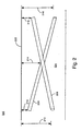
- FIG. 3 is a side sectional view of an exemplary capacitive sensor pattern 300 in accordance with embodiments of the invention.
- sensor pattern 300 includes sensing elements 310 and 320 which can be utilized as part of a capacitive sensor apparatus (e.g., 100), such as but not limited to, a touchpad.
- sensor pattern 300 provides positioning information which can be derived from which sensing element detects an object (e.g., a user's finger, a probe, and the like), and the proportional strength of the signals on sensing elements 310 and 320.
- Sensing elements 310 and 320 can be twisted about a common axis.
- Figure 3A is a general cross sectional view at section 3A-3A showing sensing element 310 located above sensing element 320 while
- Figure 3B is a general cross sectional view at section 3B-3B showing sensing element 310 located to the left of sensing element 320.
- Figure 3C is a general cross sectional view at section 3C-3C showing sensing element 310 located beneath sensing element 320 while
- Figure 3D is a general cross sectional view at section 3D-3D showing sensing element 310 located to the right of sensing element 320.
- Figure 3E is a general cross sectional view at section 3E-3E showing sensing element 310 located above sensing element 320.
- sections 3A-3A and 3E-3E show sensing elements 310 and 320 similarly situated, it may be desirable to have one of these sections outside the sensing region (e.g., 108) of a capacitive sensing apparatus in order to eliminate the possibility of sensing circuitry receiving similar strength signals that correspond to two different positions of sensor pattern 300.
- each of sensing elements 310 and 320 can have a substantially constant width along its length and is configured to have varying capacitive coupling to an object proximate to a capacitive sensing reference surface 302 along a first axis (e.g., X axis) of the reference surface 302. Note that the length of each of sensing elements 10 and 320 can be oriented along the first axis.
- the sensing elements 310 and 320 can be conductive, and are configured to provide information corresponding to a spatial location of the object relative to the first axis of the capacitive sensing reference surface 302. Sensing elements 310 and 320 can separately provide the information corresponding to the spatial location of the object.
- the capacitive coupling associated with sensing element 310 can vary with the varying distance of portions of sensing element 310 with respect to the capacitive sensing reference surface 302. Additionally, the capacitive coupling associated with the sensing element 320 can vary with the varying distance of portions of sensing element 320 with respect to the capacitive sensing reference surface 302. Note that the varying distance of the portions of sensing element 310 are different from the varying distance of the portions of sensing element 320.
- the capacitive coupling of sensing element 310 can include a first waveform (e.g., sinusoidal waveform) while the capacitive coupling of sensing element 320 can include a second waveform (e.g., sinusoidal waveform).
- the capacitive coupling of sensing element 310 can include a first phase while the capacitive coupling of sensing element 320 can include a second phase different from the first phase.
- the capacitive coupling of sensing element 310 can be 180 degrees out of phase with the capacitive coupling of sensing element 320.
- any waveform mentioned herein with reference to embodiments in accordance with the invention can be implemented in a wide variety of ways.
- a waveform can be implemented as, but is not limited to, a sinusoidal waveform, a triangular waveform, etc. It is appreciated that these exemplary waveforms are In no way an exhaustive listing of waveforms that can be Implemented as part of embodiments in accordance with the invention. It is noted that every continuous function can be a waveform in accordance with embodiments of the invention.
- each of sensing elements 310 and 320 can include a strip of conductive material. Additionally, the strip of conductive material of sensing element 310 and the strip of conductive material of sensing element 320 can be twisted about a common axis. Therefore, when sensing element 310 is coupled with sensing circuitry (e.g., 110), it can have varying capacitive coupling to an object proximate to the sensing reference surface 302 as the object moves along the length of sensing element 310. As such, a different signal strength is provided by sensing element 310 that is associated with each position or location along its length. It is understood that when sensing element 320 is coupled with sensing circuitry (e.g., 110), it can operate in a manner similar to sensing element 310, as described above.
- sensing elements 310 and 320 of sensor pattern 300 can be embedded within a substrate material (e.g., 304).
- the distance (or depth) 340 that sensing element 310 is separated from the capacitive sensing reference surface 302 varies along the length of sensing element 310.
- the distance (or depth) 330 that sensing element 320 is separated from the capacitive sensing reference surface 302 varies along the length of sensing element 320.
- sensing element 310 since the conductive strips of sensing elements 310 and 320 are twisted about a common axis, it is noted that depending on the location of sensing element 310, it can interfere with the capacitive coupling with an object of sensing element 320 (and vice versa). For example, if an object was proximately located to reference surface 302 at section 3A-3A, sensing element 310 would shield (or limit) the capacitive coupling that sensing element 320 would have to the object since sensing element 310 is located between sensing element 320 and the object.
- sensing element 320 would shield (or limit) the capacitive coupling that sensing element 310 would have to the object since sensing element 320 is located between sensing element 310 and the object.
- FIG. 4 is a side sectional view of an exemplary capacitive sensor pattern 400 in accordance with embodiments of the invention.
- sensor pattern 400 includes sensing elements 410, 420, and 430 which can be utilized as part of a capacitive sensor apparatus or device (e.g., 100), such as but not limited to, a touchpad.
- sensor pattern 400 provides positioning information which can be derived from which sensing element detects an object (e.g., a user's finger, a probe, and the like), and the proportional strength of the signals on sensing elements 410, 420, and 430.
- Sensing elements 410, 420, and 440 can be twisted about a common axis.
- Figure 4A is a general cross sectional view at section 4A-4A showing sensing element 430 located to the left of sensing element 420 and sensing element 410 located above sensing elements 420 and 430.
- Figure 4B is a general cross sectional view at section 4B-4B showing sensing element 410 located to the left of sensing element 420 and sensing element 430 located beneath sensing elements 410 and 420.
- Figure 4C is a general cross sectional view at section 4C-4C showing sensing element 410 located to the left of sensing element 430 and sensing element 420 located above sensing elements 410 and 430.
- Figure 4D is a general cross sectional view at section 4D-4D showing sensing element 420 located to the left of sensing element 430 and sensing element 410 located beneath sensing elements 420 and 430.
- Figure 4E is a general cross sectional view at section 4E-4E showing sensing element 420 located to the left of sensing element 410 and sensing element 430 located above sensing elements 410 and 420.
- Figure 4F is a general cross sectional view at section 4F-4F showing sensing element 430 located to the left of sensing element 410 and sensing element 420 located beneath sensing elements 410 and 430.
- Figure 4G is a general cross sectional view at section 4G-4G showing sensing element 430 located to the left of sensing element 420 and sensing element 410 located above sensing elements 420 and 430.
- sections 4A-4A and 4E-4E show sensing elements 410, 420, and 430 similarly situated, It may be desirable to have one of these sections outside the sensing region (e.g., 108) of a capacitive sensing apparatus (e.g., 100) in order to eliminate the possibility of sensing circuitry (e.g., 110) receiving similar strength signals that correspond to two different positions (or locations) of sensor pattern 400.
- each of sensing elements 410, 420, and 430 has varying depth relative to a capacitive sensing reference surface 402 and are substantially parallel to each other.
- sensing elements 420 and 430 are substantially parallel to sensing element 410.
- Each of sensing elements 410, 420, and 430 can have varying depth (or distance) relative to reference surface 402 and each can include a waveform.
- the waveform of sensing element 420 can be offset from the waveform of sensing element 410 by one third of a period.
- the waveform of sensing element 430 can be offset from the waveform of sensing element 410 by two thirds of a period.
- the sensing elements 410, 420, and 430 can be configured to provide (e.g., sensing circuitry) information corresponding to a position of an object proximate to the capacitive sensing reference surface 402 along a first axis of the capacitive sensing reference surface 402.
- the sensing elements 410, 420, and 430 can each include a conductive trace. Portions of each of sensing elements 410, 420, and 430 can be configured to have a capacitive coupling with respect to the object wherein the capacitive coupling varies along the first axis.
- the position of the object can be determined using a signal corresponding to sensing element 410, a signal corresponding to sensing element 420, and a signal corresponding to sensing element 430.
- the sensing elements 410, 420, and 430 can provide a cumulative output signal that is substantially constant at different locations along the sensing elements 410, 420, and 430.
- Each of sensing elements 410, 420, and 430 can include a strip of conductive material. Additionally, the strip of conductive material of sensing element 410, the strip of conductive material of sensing element 420, and the strip of conductive material of sensing element 430 can be twisted about a common axis.
- sensing element 410 when sensing element 410 is coupled with sensing circuitry (e.g., 110), it can have varying capacitive coupling to an object proximate to the sensing reference surface 402 as the object moves along the length of sensing element 410. As such, a different signal strength is provided by sensing element 410 that is associated with each position or location along its length. It is appreciated that when sensing elements 420 and 430 are coupled with sensing circuitry (e.g., 110), they can operate in a manner similar to sensing element 410, as described above.
- Figure 6 illustrates an exemplary signal strength chart 602 along with its conversion into polar coordinates in accordance with embodiments of the invention. For example, suppose signal "A” is associated with sensing element 410 ( Figure 4 ), signal “B” is associated with sensing element 420, and signal “C” is associated with sensing element 430.
- the object is located along sensor 400 where sensing trace 420 is nearest to sensing surface 402, the sensing trace 410 Is the second nearest to sensing surface 402, and the sensing trace 430 is the farthest from sensing surface 402. Therefore, within this example, the object is located on the right-hand side of the section 4C-4C of sensor pattern 400.
- sensing element 410 corresponds to sensing element 410
- signal “B” corresponds to sensing element 420
- signal “C” corresponds to sensing element 430
- sensing elements (or traces) 410, 420, and 430 have been observed to give values A 0 , B 0 , and C 0 , respectively, when no object is present or near sensor pattern 400.
- a A - A 0
- b B - B 0
- c C - C 0 . Therefore, determination of the polar coordinates "h”, "r”, and angle ⁇ that are associated with signals A, B, and C can be performed.
- the value of "h” corresponds to the height of the center of a circle 604 upon which points 606, 608, and 610 can be located.
- the points 606, 608, and 610 are associated with signals A, B, and C, respectively.
- the value of "r” corresponds to the radius of circle 604.
- the value of angle ⁇ can be used to ascertain the linear location (or position) of an object in relationship (or proximity) to the length of sensor pattern 400.
- each degree of angle ⁇ may be equal to a specific distance (e.g., a specific number of millimeters or inches) from one of the end points of sensor pattern 400.
- a lookup table may be utilized to ascertain the distance that corresponds to the determined ⁇ . It is noted that the angle ⁇ can provide the location of the center of the object along sensor pattern 400 while the "h” and the “r” can provide information regarding the size of the object.
- One of the advantages of determining the position along the first axis (e.g., X axis) of sensor pattern 400 in the manner described above is that common-mode noise has no effect on the determination of "r" and ⁇ .
- sensing elements 410, 420, and 430 of sensor pattern 400 can be embedded within a substrate material (e.g., 404).
- a substrate material e.g., 404
- the distance (or depth) 440 that sensing element 420 is separated from the capacitive sensing reference surface 402 varies along the length of sensing element 420.
- the distance (or depth) 450 that sensing element 430 is separated from the capacitive sensing reference surface 402 varies along the length of sensing element 430.
- sensing element 410 can be implemented in a manner similar to sensing elements 420 and 430.
- sensing elements 410, 420, and 430 are twisted about a common axis, it is noted that depending on their location, two of them can interfere with the capacitive coupling with an object of the remaining sensing element. For example, if an object was proximately located to reference surface 402 at section 4D-4D, sensing elements 420 and 430 would shield (or limit) the capacitive coupling that sensing element 410 would have to the object since sensing element 420 and 430 are located between sensing element 410 and the object.
- FIG. 5 is a side sectional view of an exemplary capacitive sensor pattern 500 in accordance with embodiments of the present invention.
- sensor pattern 500 includes sensing elements 510 and 530 which can be utilized as part of a capacitive sensor apparatus (e.g., 100), such as but not limited to, a touchpad.
- sensor pattern 500 provides positioning information which can be derived from which sensing element detects an object (e.g., a user's finger, a probe, and the like), and the proportional strength of the signals on sensing elements 510 and 530.
- Sensing elements 510 and 530 can be twisted about a mandrel 520 that provides them a common axis.
- Figure 5A is a general cross sectional view at section 5A-5A showing sensing element 510 located above mandrel 520 which is located above sensing element 530.
- Figure 5B is a general cross sectional view at section 5B-5B showing sensing element 510 located to the left of mandrel 520 and sensing element 530 located to the right of mandrel 520.
- Figure 5C is a general cross sectional view at section 5C-5C showing sensing element 510 located beneath mandrel 520 which is located beneath sensing element 530.
- Figure 5D is a general cross sectional view at section 5D-5D showing sensing element 510 located to the right of mandrel 520 and sensing element 530 located to the left of mandrel 520.
- Figure 5E is a general cross sectional view at section 5E-5E showing sensing element 510 located above mandrel 520 which is located above sensing element 530.
- sections 5A-5A and 5E-5E show mandrel 520 and sensing elements 510 and 530 similarly situated, it may be desirable to have one of these sections outside the sensing region (e.g., 108) of a capacitive sensing apparatus (e.g., 100) in order to eliminate the possibility of sensing circuitry (e.g., 110) receiving similar strength signals that correspond to two different positions of sensor pattern 500.
- a capacitive sensing apparatus e.g., 100
- each of sensing elements 510 and 530 can have a substantially constant width along its length and is configured to have varying capacitive coupling to an object proximate to a capacitive sensing reference surface 502 along a first axis (e.g., X axis) of the reference surface 502.
- first axis e.g., X axis
- the length of each of sensing elements 510 and 530 can be oriented along the first axis (e.g., mandrel 520).
- the sensing elements 510 and 530 can be conductive, and are configured to provide information corresponding to a spatial location of the object relative to the first axis of the capacitive sensing reference surface 502. Sensing elements 510 and 530 can separately provide the information corresponding to the spatial location of the object.
- the capacitive coupling associated with sensing element 510 can vary with the varying distance of portions of sensing element 510 with respect to the capacitive sensing reference surface 502. Additionally, the capacitive coupling associated with the sensing element 530 can vary with the varying distance of portions of sensing element 530 with respect to the capacitive sensing reference surface 502. Note that the varying distance of the portions of sensing element 510 are different from the varying distance of the portions of sensing element 530.
- the capacitive coupling.of sensing element 510 can include a first waveform (e.g., sinusoidal waveform) while the capacitive coupling of sensing element 530 can include a second waveform (e.g., sinusoidal waveform). Note that every continuous function can be a waveform.
- the capacitive coupling of sensing element 510 can include a first phase while the capacitive coupling of sensing element 530 can include a second phase different from the first phase.
- the capacitive coupling of sensing element 510 can be 180 degrees out of phase with the capacitive coupling of sensing element 530, but is not limited to such.
- each of sensing elements 510 and 530 can include a strip of conductive material. Additionally, the strip of conductive material of sensing element 510 and the strip of conductive material of sensing element 530 can be twisted about mandrel 520. Therefore, when sensing element 510 is coupled with sensing circuitry (e.g., 110), it can have varying capacitive coupling to an object proximate to the sensing reference surface 502 as the object moves along the length of sensing element 510. As such, a different signal strength is provided by sensing element 510 that is associated with each position or location along its length. It is understood that when sensing element 530 is coupled with sensing circuitry (e.g., 110), it can operate in a manner similar to sensing element 510, as described above.
- sensing elements 510 and 530 of sensor pattern 500 can be embedded within a substrate material (e.g., 508).
- the distance (or depth) 506 that sensing element 510 Is separated from the capacitive sensing reference surface 502 varies along the length of sensing element 510.
- the distance (or depth) 504 that sensing element 530 is separated from the capacitive sensing reference surface 502 varies along the length of sensing element 530.
- sensing element 510 and 530 are twisted about mandrel 520, it is noted that depending on the location of sensing element 510, it and mandrel 520 can interfere with the capacitive coupling with an object of sensing element 530 (and vice versa). For example, if an object was proximately located to reference surface 502 at section 5A-5A, sensing element 510 and mandrel 620 would shield (or limit) the capacitive coupling that sensing element 630 would have to the object since sensing element 510 and mandrel 520 are located between sensing element 530 and the object.
- sensing element 530 and mandrel 520 would shield (or limit) the capacitive coupling that sensing element 510 would have to the object since sensing element 530 and mandrel 520 are located between sensing element 510 and the object.
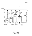
- Figures 7A-7E are described in combination in order to provide a better understanding of an exemplary capacitive sensor pattern 700a, in accordance with embodiments of the invention.
- Figure 7A is a cross sectional view of capacitive sensor pattern 700a in accordance with embodiments of the invention.
- Figures 7B, 7C, 7D, 7E are lengthwise side sectional views 700b, 700c, 700d, and 700e, respectively, of capacitive sensor pattern 700a in accordance with embodiments of the invention.
- Sensor pattern 700a includes sensing elements 706, 708, 710, and 712 which can be utilized as part of a two-dimensional capacitive sensor apparatus (e.g., 100), such as but not limited to, a touchpad.
- sensor pattern 700a provides positioning information from a sensor pattern that has substantially parallel traces (or elements) with no crossovers. The positioning information can be derived from which sensing element or elements detect an object (e.g., a user's finger, a probe, and the like) proximate to a sensing reference surface 702, and the proportional strength of the signals on sensing elements 706, 708, 710, and 712.
- an object e.g., a user's finger, a probe, and the like
- capacitive sensor pattern 700a can include an insulating substrate material 704 having a substantially smooth, planar capacitive sensing reference surface 702 where an object (e.g., a user's finger, a probe, and the like) can contact or be proximately located thereto.
- the substrate 704 includes substantially parallel channels (or grooves) 730, 732, 734, and 736.
- channels 732, 734, and 736 can be implemented to include three phases. However, along the length of groove 730, its distance from reference surface 702 can be substantially constant.
- sensing elements 710, 712, and 708 can each include a waveform that varies in distance from reference surface 702 as shown in Figures 7B, 7C, and 7D , respectively.
- sensing elements (or traces) 708, 710, and 712 can be used to determine a position of an object relative to a first axis (e.g., X axis) of the sensing reference surface 702 while sensing element 706 can be used to determine a position of the object relative to a second axis (e.g., Y axis) of the reference surface 702.
- the second axis may be non-parallel (e.g., substantially perpendicular) to the first axis.
- a conductive material can be deposited within channels 730, 732, 734, and 736 to produce sensing elements 706, 708, 710, and 712, respectively.
- each of sensing elements 708, 710, and 712 can be disposed above substrate 704, wherein the varying depths of channels 732, 734, and 736 define a unique depth (or distance) profile for each of sensing elements 708, 710, and 712, respectively.
- the deposition of the conductive material may be Implemented In a wide variety of ways (e.g., printing, spraying on, painting on, and the like).
- the sensing elements 706, 708, 710, and 712 can be formed by the deposition of any one conductive material or may include layers of conductive materials such as, but not limited to, black chrome, aluminum, titanium, and the like. Although the foregoing materials are mentioned specifically, it is understood that any conductive material that can be deposited into channels 730, 732, 734, and 736 to form sensing elements 706, 708, 710, and 712, respectively, can be used.
- Sensing elements (or traces) 708, 710, and 712 have varying depths 722, 724, and 726, respectively, with respect to sensing reference surface 702. However, sensing element (or trace) 706 has a substantially constant depth 720 with respect to sensing reference surface 702.
- sensing elements 708, 710, and 712 each includes a waveform having varying depth (or distance) from reference surface 702, each of which has a different phase. For example, within the present embodiment, if the waveform shape of conductive trace 708 is substantially equal to sin ⁇ , then the waveform shape of conductive trace 710 may be substantially equal to sin ( ⁇ + 120 degrees), while the waveform shape of conductive trace 712 may be substantially equal to sin ( ⁇ + 240 degrees).
- the waveform of sensing element 710 may be offset (or shifted) from the waveform of conductive trace 708 by 2 ⁇ /3 radians while the waveform of sensing element 712 may be offset (or shifted) from the waveform of conductive trace 708 by 4 ⁇ /3 radians.
- the waveform of sensing element 710 can be offset from the waveform of sensing element 708 by one third of a period while the waveform of sensing element 712 can be offset from the waveform of sensing element 708 by two thirds of a period.
- the phase and shape of the waveform of sensing elements 708, 710, and 712 are not in any way limited to the present embodiment or the recited embodiments.
- the position of the object can be determined using a signal corresponding to sensing element 708, a signal corresponding to sensing element 710, and a signal corresponding to sensing element 712.
- the sensing elements 708, 710, and 712 can provide a cumulative output signal that is substantially constant at different locations along the sensing elements 708, 710, and 712.
- the determination of the location (or position) of an object in relation to the length of sensor pattern 700a can be implemented in a manner similar to that described herein with reference to Figures 4 and 6 , but is not limited to such.
- capacitive sensor pattern 700a may have been fabricated utilizing a process 1600 of Figure 16 described below, or by other processes (e.g., that may include machining an insulating material with the desired depth variations).
- FIG 8 is a plan view of an exemplary capacitive sensor pattern 800 including electrical connections, in accordance with embodiments of the invention.
- sensor pattern 800 includes four repeating sets of sensing elements 706, 708, 710, and 712. Note that sensing elements 708, 710, and 712 can each have varying depth (or distance) from the sensing reference surface (not shown) while sensing element 706 can have a substantially constant depth (or distance) from the sensing reference surface.
- the sensing elements 708, 710, and 712 can include waveforms that have three phases, but are not limited to such.
- each of sensing elements 708 is coupled with electrical trace 810
- each of sensing elements 710 is coupled with trace 820
- each of sensing elements 712 is coupled with trace 830.
- each of sensing elements 706 is coupled independently with traces 840. Traces 810, 820, 830, and 840 can be coupled with traces 104 and/or 106 of Figure 1 .
- the sensor pattern 800 can be utilized to form the sensing region 108.
- Sensing elements 708, 710, and 712 can be used to determine the x-position, or first axis location, of an object (e.g., a finger, a probe, a stylus, etc.) relative to sensor pattern 800.
- Sensing elements 706 can be used to determine the y-position, or second axis location, of an object (e.g., a finger, a probe, a stylus, etc.) relative to sensor pattern 800.
- each of sensing elements 708, 710, and 712 can be coupled independently with sensing circuitry (e.g., 110), in which case the y-position of an object could be determined directly from each trace.
- each sensing element 706 may be excluded from sensor pattern 800.
- This method of electrically coupling each of traces 708, 710, and 712 of sensor pattern 800 independently may involve more than one Application Specific Integrated Circuit (ASIC) if the number of sensing elements is large, whereas the method of interconnecting all sensing elements having the same varying depth and phase, then using intermediate sensing elements 706 to determine the y-position allows a larger number of sensing elements to be used in conjunction with a single ASIC.
- ASIC Application Specific Integrated Circuit
- the sensor pattern 800 can also be implemented with guard trace 850 at the "top” and guard trace 852 at the "bottom” of sensor pattern 800, thereby enabling the "edge" sensing elements located near them to operate in a manner similar to those sensing elements more centrally located within the sensor pattern 800.
- the guard traces 850 and 852 may be electrically driven, grounded and/or held at a substantially fixed or constant potential in accordance with embodiments of the present invention.
- guard traces 850 and 852 of Figure 8 may be coupled to ground via traces 854 and 856, respectively; in this manner, guard traces 850 and 852 are functioning as grounded traces.
- guard traces 850 and 852 may be coupled to a constant potential signal via traces 854 and 856, respectively; in this manner, guard traces 850 and 852 are functioning as constant potential traces.
- Guard traces 850 and 852 may also be actively driven via traces 854 and 856, respectively; in this manner, guard traces 850 and 852 are functioning as driven guard traces. It is understood that guard traces 850 and 852 may be implemented in a wide variety of ways.
- guard traces (or grounded or fixed potential traces) similar to guard traces 850 and 852 can also be included as part of or with any sensing pattern described herein.
- sensor pattern 800 of Figure 8 indicates using repeated sets of three sensing elements to determine the x-position (e.g., first axis) of an object relative to sensor pattern 800, it should be understood that a different number of sensing elements may be employed, using an appropriate mathematical relationship, to discern the x-position of an object.
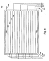
- FIG. 9 is a plan view of an exemplary sensor pattern 900 in accordance with embodiments of the invention.
- Sensor pattern 900 includes six repeated patterns of sensing elements 708, 710, and 712. Specifically, sensing elements 708, 710, and 712 can each have varying depth (or distance) from the sensing reference surface (not shown).
- the sensing elements 708, 710, and 712 can include waveforms having three phases.
- Sensing elements 708, 710, and 712 can be utilized as part of a single layer capacitive sensor apparatus (e.g., 100), such as but not limited to, a touchpad.
- sensor pattern 900 can provide two-dimensional positioning information that has substantially parallel traces (or sensing elements) with no crossovers.
- the sensor pattern 900 can be utilized in any manner similar to that described herein, but is not limited to such.
- sensing elements 708, 710, and 712 can operate in any manner similar to sensing elements 708, 710, and 712 of sensor pattern 800 of Figure 8 , described herein.
- FIGS 10A and 10B are side sectional views of an exemplary capacitive sensor pattern 1000
- sensor pattern 1000 Includes sensing elements 1020 and 1022 which can be utilized as part of a capacitive sensor apparatus (e.g., 100) such as, but not limited to, a touchpad.
- sensor pattern 1000 provides positioning information which can be derived from which sensing element detects an object (e.g., a user's finger, a probe, and the like), and the proportional strength of the signals on sensing elements 1020 and 1022.
- Each of sensing elements 1020 and 1022 can have a substantially constant width along its length and is configured to have varying capacitive coupling to an object proximate to a capacitive sensing reference surface 1002 along a first axis (e.g., X axis) of the reference surface 1002.
- the capacitive coupling of sensing element 1020 can vary with variations in dielectric constant between the capacitive sensing reference surface 1002 and portions of sensing element 1020.
- the capacitive coupling of sensing element 1022 can vary with variations in dielectric constant between the capacitive sensing reference surface 1002 and portions of sensing element 1022.
- sensing elements 1020 and 1022 can each have a substantially constant depth (or distance) from the sensing reference surface 1002, while each can be configured to have varying capacitive coupling to an object proximate to sensing reference surface 1002.
- each of sensing elements 1020 and 1022 can be oriented along the first axis.
- the sensing elements 1020 and 1022 can be conductive, and are configured to provide information corresponding to a spatial location of the object relative to the first axis of the capacitive sensing reference surface 1002. Note that sensing elements 1020 and 1022 can separately provide the information corresponding to a spatial location of the object.
- sensing elements 1020 and 1022 can include a strip of conductive material that is substantially straight along the first axis. Specifically, within Figure 10A , sensing element 1020 is disposed above a substrate 1008, while a dielectric material 1006 is disposed above sensing element 1020, and a dielectric material 1004 is disposed above dielectric material 1006. Note that the upper surface of dielectric material 1006 increasingly slopes away from capacitive sensing reference surface 1002.
- sensing element 1020 can have a stronger capacitive coupling to an object proximate to the left-hand side of capacitive sensing reference surface 1002 than when proximate to its right-hand side. Therefore, when sensing element 1020 is coupled with sensing circuitry (e.g., 110), it can have varying capacitive coupling to an object proximate to the sensing reference surface 1002 as the object moves along the length of sensing element 1020. As such, a different signal strength is provided by sensing element 1020 that is associated with each position or location along its length.
- sensing element 1022 is disposed above substrate 1008, while a dielectric material 1010 is disposed above sensing element 1022, and a dielectric material 1012 is disposed above dielectric material 1010. Note that the upper surface of dielectric material 1010 increasingly slopes away from capacitive sensing reference surface 1002. Given that dielectric material 1010 has a lower dielectric constant than dielectric material 1012 and sensing element 1022 is coupled to sensing circuitry (e.g., 110), sensing element 1022 can have a stronger capacitive coupling to an object proximate to the left-hand side of capacitive sensing reference surface 1002 than when proximate to its right-hand side.
- sensing element 1022 when sensing element 1022 is coupled with sensing circuitry (e.g., 110), it can have varying capacitive coupling to an object proximate to the sensing reference surface 1002 as the object moves along the length of sensing element 1022. As such, a different signal strength is provided by sensing element 1022 that is associated with each position or location along its length.
- dielectric materials 1004, 1006, 1010, and 1012 can be implemented with differing dielectric constants.
- sensing circuitry e.g., 110
- the proportional strength signals provided by them can be unique as an object proximately located to sensing reference surface 1002 travels along the length of sensing elements 1020 and 1022. Therefore, the sensing circuitry can identify the spatial location of the object relative to the first axis of the capacitive sensing reference surface 1002.
- FIG 11 is a plan view of an exemplary loop capacitive sensor pattern 1100 in accordance with embodiments of the invention.
- sensor pattern 1100 includes three sets of concentric loop patterns of sensing elements 708a, 710a, and 712a that can include waveforms having three phases.
- the sensor pattern 1100 can be utilized as part of a single layer capacitive sensor apparatus (e.g., 100), such as but not limited to, a touch pad.
- sensor pattern 1100 can provide continuous two-dimensional positioning information that has sensing elements with varying depth and no crossovers.
- the sensor pattern 1100 can be utilized in any manner similar to that described herein, but is not limited to such.
- each of the sensing elements 708a, 710a, and 712a has varying depth (or distance) from the sensing reference surface (not shown) and form a substantially circular (or loop) pattern.
- a loop pattern may include any closed loop sensor pattern shape (e.g., circle, square, rectangle, triangle, polygon, radial arc sensor pattern, curve, a semi-circle sensor pattern, and/or any sensor pattern that is not substantially in a straight line or in a non-linear manner).
- the sensing elements 708a, 710a, and 712a are not required to overlap each other in order to determine an angular position ⁇ of an object relative to the substantially circular pattern (e.g., loop) in a two-dimensional space.
- the angular position ⁇ starts at an origin 1102 which can be located anywhere associated with sensor pattern 1100.
- the sensing elements 708a, 710a, and 712a can provide a cumulative output signal that is substantially constant at different locations along the sensing elements 708a, 710a, and 712a.
- the sensing elements 708a, 710a, and 712a can each include a conductive trace. Furthermore, each set of sensing elements (e.g., 708a, 710a, and 712a) can be used for determining a radial position "R" of the object relative to the loop in the two-dimensional space.
- Each of the sensing elements (e.g., 708a, 710a, and 712a) of the sensor pattern 1100 can be individually coupled with sensing circuitry (e.g., 110) utilizing conductive coupling traces (e.g., 104 and/or 106). When coupled in this manner, the sensor pattern 1100 can be utilized to form a sensing region (e.g., 108). Furthermore, when coupled in this manner, sensor pattern 1100 can provide positioning information along the angular position ⁇ and the radial position "R".
- sensing elements e.g., 712a
- sensing circuitry e.g., 110
- a conductive coupling trace e.g., 104 or 106
- the sensor pattern 1100 can provide positioning information to the sensing circuitry corresponding to the angular position ⁇ , but not of the radial position "R". It is understood that the radial position "R" can be determined in any manner similar to the way the second axis position can be determined, as described herein.
- Sensor pattern 1100 can be implemented with a greater or lesser number of sensing elements than shown within the present embodiment.
- sensor pattern 1100 can be implemented with a single set of sensing elements 708a, 710a, and 712a.
- sensor pattern 1100 can be implemented with multiple sets of sensing elements 708a, 710a, and 712a.
- Sensor pattern 1100 and its sensing elements can be implemented in any manner similar to that described herein, but is not limited to such.
- each set of the sensing elements (e.g., 708a, 710a, and 712a) of sensor pattern 1100 can operate in any manner similar to that described herein in order to provide the positioning information corresponding to the angular position ⁇ of an object (e.g., a user's finger, a probe, a stylus, and the like) in relation to sensor pattern 1100.
- the sensing elements 708a, 710a, and 712a can be configured to provide information corresponding to a spatial location of the object proximate to a curve on said capacitive sensing reference surface (not shown).
- each set of the signals associated with a set of sensing elements can be utilized to determine the phase angle ⁇ , in a manner similar to that described herein with reference to Figure 6 .
- the phase angle ⁇ may be converted into a geometric position angle ⁇ relative to the origin 1102. In this manner, the angular position ⁇ of an object is determined relative to sensor pattern 1100.
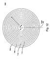
- FIG. 12 illustrates an exemplary loop capacitive sensor pattern 1200 in accordance with embodiments of the present invention.
- sensor pattern 1200 Includes three sets of concentric loop patterns of sensing elements 706b, 708b, 710b, and 712b. Note that sensing elements 708b, 710b, and 712b can each have varying depth (or distance) from the sensing reference surface (not shown) while sensing element 706b can have a substantially constant depth from the reference surface.
- the sensing elements 708b, 710b, and 712b can include waveforms having three phases.
- Sensor pattern 1200 can be utilized as part of a single layer capacitive sensor apparatus (e.g., 100), such as, but not limited to, a touch pad. When electrically coupled, sensor pattern 1200 can provide continuous two-dimensional positioning information that has sensing elements with varying depth and no crossovers.
- the sensor pattern 1200 can be utilized in any manner similar to that described herein, but is not limited to such.
- sensing elements 706b, 708b, 710b, and 712b form a substantially circular (or loop) pattern.
- a loop pattern may include any closed loop sensor pattern shape (e.g., circle, square, rectangle, triangle, polygon, radial arc sensor pattern, a semi-circle sensor pattern, and/or any sensor pattern that is not substantially in a straight line).
- the sensing elements 706b, 708b, 710b, and 712b are not required to overlap each other in order to determine an angular position ⁇ and radial position "R" of an object relative to the substantially circular pattern (e.g., loop) in a two-dimensional space.
- the angular position ⁇ starts at an origin 1202 which can be located anywhere associated with sensor pattern 1200.
- the sensing elements 708b, 710b, and 712b provide a cumulative output signal that can be substantially constant at different locations along the sensing elements 708b, 710b, and 712b.
- the sensing elements 706b, 708b, 710b, and 712b can each include a conductive trace. Similar varying depth sensing elements (e.g., 708b) of sensor pattern 1200 can be coupled together as shown in Figure 8 and coupled with sensing circuitry (e.g., 110) utilizing a conductive coupling trace (e.g., 104 or 106). When coupled in this manner, the sensor pattern 1200 can provide positioning information to the sensing circuitry corresponding to the angular position ⁇ , but not of the radial position "R". It is understood that the radial position "R" can be determined from sensors 706b in any manner similar to the way the second axis position can be determined, as described herein.
- Sensor pattern 1200 can be implemented with a greater or lesser number of sensing elements than shown within the present embodiment.
- sensor pattern 1200 can be implemented with a single set of sensing elements 706b, 708b, 71 0b, and 712b.
- sensor pattern 1200 can be implemented with multiple sets of sensing elements 706b, 708b, 710b, and 712b.
- Sensor pattern 1200 and its sensing elements can be Implemented In any manner similar to that described herein, but is not limited to such.
- each set of the varying depth sensing elements 706b, 708b, 710b, and 712b of sensor pattern 1200 can operate in any manner similar to that described herein in order to provide the positioning information corresponding to the angular position ⁇ of an object (e.g., a user's finger, a probe, a stylus, and the like) in relation to sensor pattern 1200.
- each set of the signals associated with the set of varying depth sensing elements 708b, 710b, and 712b can be utilized to determine the phase angle ⁇ , in a manner similar to that described herein with reference to Figure 6 . Noted that once the phase angle ⁇ has been determined, it may be converted into a geometric position angle ⁇ relative to the origin 1202. In this manner, the angular position ⁇ of an object is determined relative to sensor pattern 1200.
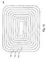
- FIG. 13 is a plan view of an exemplary loop capacitive sensor pattern 1300 in accordance with embodiments of the invention.
- sensor pattern 1300 includes three sets of concentric loop patterns of sensing elements 708c, 710c and 712c. Note that sensing elements 708c, 710c, and 712c can each have varying depth or distance from the reference surface (not shown).
- the sensing elements 708c, 710c, and 712c can be implemented to include waveforms having three phases.
- the sensing elements 708c, 710c, and 712c can be utilized as part of a single layer capacitive sensor apparatus (e.g., 100), such as but not limited to, a touchpad.
- sensor pattern 1300 can provide continuous two-dimensional positioning information that has sensing elements with varying depth and no crossovers.
- the sensor pattern 1300 can be utilized in any manner similar to that described herein, but is not limited to such.
- sensor pattern 1300 can operate In any manner similar to sensor pattern 1100 of Figure 11 .
- the sensor pattern 1300 can be Implemented with a greater or lesser number of sensing elements than shown within the present embodiment.
- Sensor pattern 1300 and its sensing elements can be implemented in any manner similar to that described herein, but is not limited to such.
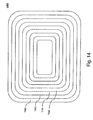
- FIG 14 is a plan view of an exemplary loop capacitive sensor pattern 1400 in accordance with embodiments of the invention.
- sensor pattern 1400 includes two sets of concentric loop patterns of sensing elements 706d, 708d, 710d, and 712d.
- sensing elements 708d, 710d, and 712d can each have varying depth or distance from the reference surface (not shown) while sensing element 706d can have a substantially constant depth or distance from the reference surface.
- the sensing elements 708d, 710d, and 712d can be implemented to include waveforms in three phases.
- sensing elements 706d, 708d, 710d, and 712d can be utilized as part of a capacitive sensor apparatus (e.g., 100), such as but not limited to, a touchpad.
- sensor pattern 1400 can provide continuous two-dimensional positioning information that has sensing elements with varying depth and no crossovers.
- the sensor pattern 1400 can be utilized in any manner similar to that described herein, but is not limited to such.
- sensor pattern 1400 can operate in any manner similar to sensor patterns 1100 ( Figure 11 ) and/or 1200 ( Figure 12 ).
- the sensor pattern 1400 can be Implemented with a greater or lesser number of sensing elements than shown within the present embodiment.
- Sensor pattern 1400 and its sensing elements can be implemented in any manner similar to that described herein, but is not limited to such.
- FIG. 15 is a plan view of an exemplary "fishbone" capacitive sensor pattern 1500 in accordance with embodiments of the invention.
- sensor pattern 1500 includes a set of sensing elements 708e, 710e, and 712e that can be utilized as part of a capacitive sensor apparatus (e.g., 100), such as but not limited to, a touchpad.
- sensing elements 708e, 710e, and 712e can each have varying depth (or distance) from a sensing reference surface (not shown).
- sensor pattern 1500 can provide two-dimensional positioning information that has substantially parallel traces (or sensing elements) with no crossovers.
- the sensor pattern 1500 can be utilized in any manner similar to that described herein with reference to Figures 7A-7E , 8 , and 9 , but is not limited to such. Moreover, sensor pattern 1500 can be utilized in any manner similar to that described herein, but is not limited to such.
- sensing element 708e can include a plurality of extensions 1502 that are substantially parallel to each other and are substantially perpendicular to a first axis of sensing element 708e.
- the sensing element 710e can include a plurality of extensions 1504 that are substantially parallel to each other and are substantially perpendicular to the first axis of sensing element 71 0e.
- the sensing element 712e can include a plurality of extensions 1506 that are substantially parallel to each other and are substantially perpendicular to the first axis of sensing element 712e.
- the plurality of extensions 1502 of sensing element 708e can be interdigitated with the plurality of extensions 1504 of sensing element 710e.
- the plurality of extensions 1506 of sensing element 712e can be interdigitated with the plurality of extensions 1504 of sensing element 710e.
- Sensing elements 708e, 710e, and 712e can be used for determining a first location of an object (e.g., a user's finger, a probe, a stylus, and the like) in relation to sensor pattern 1500 along the first axis of a two-dimensional space. Furthermore, a repeated set of sensing elements 708e, 710e, and 712e (not shown) can be used for determining first and second locations of an object in relation to sensor pattern 1500 along the first axis and a second axis of the two-dimensional space, wherein the second axis is substantially non-parallel (or substantially perpendicular) to the first axis.
- an object e.g., a user's finger, a probe, a stylus, and the like
- a repeated set of sensing elements 708e, 710e, and 712e can be used for determining first and second locations of an object in relation to sensor pattern 1500 along the first axis and a second axis of the
- sensor pattern 1500 can operate in any manner similar to sensor patterns 700a-700e of Figures 7A-E . Additionally, the sensor pattern 1500 can be implemented with a greater or lesser number of sensing elements than shown within the present embodiment. Sensor pattern 1500 and its sensing elements can be implemented in any manner similar to that described herein, but is not limited to such.
- Figure 16 is a flowchart of a method 1600 for establishing a position-varying capacitive coupling between a conductive object proximate to a capacitive sensing reference surface and a conductive trace in accordance with embodiments of the invention.
- method 1600 may not include all of the operations illustrated by Figure 16 .
- method 1600 may include various other operations and/or variations of the operations shown by Figure 16 .
- a plurality of channel patterns can be provided (or formed) in a substrate. Note that the channel patterns varying in depth.
- a conductive material can be deposited onto the channel patterns to form a first sensing element and second sensing element.
- the first sensing element and second sensing element can be conductive and lie substantially along a first orientation.
- each of the first sensing element and second sensing element can be configured to provide information corresponding to a first location along the first orientation.
- a plurality of channel (or groove) patterns having varying depth can be provided (or formed) in a substrate.
- the substrate can be implemented in a wide variety of ways.
- the substrate can be implemented to include, but is not limited to, a plastic or a crystalline material.
- the substrate can be implemented as a component of an information display device or a portable computing device.
- the substrate can be implemented as a part of a casing or front cover of an information display device or portable computing device.
- the channel patterns can include waveforms or portions of waveforms.
- the channel patterns can include one or more sinusoidal waveforms.
- the channel patterns can include one or more portions of a sinusoidal waveform.
- a conductive material can be deposited onto the channel (or groove) patterns to form a first sensing element and second sensing element that are conductive and lie substantially along a first orientation.
- first sensing element and second sensing element can be configured to provide information corresponding to a first location along the first orientation.
- first orientation can be implemented in diverse ways.
- the first orientation can be substantially linear.
- the first orientation can be non-linear.
- the first and second sensing elements can be implemented in a wide variety of ways.
- the first sensing element can include a first waveform while the second sensing element can Include a second waveform.
- first waveform and the second waveform can be different or similar.
- the first waveform and the second waveform can each include one or more sinusoidal waveforms or a portion of a sinusoidal waveform.
- the first waveform and the second waveform can each have a different phase. It is understood that the first sensing element and second sensing element can each form at least a portion of a loop or a curve:
- the first sensing element can be backfilled with a material.
- the second sensing element may also be backfilled with a material at operation 1630.
- the backfilling material can be implemented in a wide variety of ways.
- the material can be implemented as, but not limited to, the material of which the substrate is formed, insulting material, and/or electrical shielding material.
- This optional backfilling material can provide physical protection to the one or more sensing elements.
- the backfilling material can provide electrical shielding thereby causing the one or more sensing elements to measure capacitance on a desired reference sensing surface of the substrate, instead of on both sides of the substrate.
- the backfilling material can provide a smooth back surface on the substrate that may be desirable in some circumstances.
- the capacitive sensor pattern By fabricating the capacitive sensor pattern in the manner shown in Figure 16 , failure rates can be reduced since only one layer of conductive material is utilized, and there are no crossovers in the sensing elements.
- the capacitive sensor pattern may be manufactured very inexpensively by molding the channel patterns into the case of a laptop computer or other electronic device and depositing (or printing or spraying) the conductive material onto the channel patterns.
- sensor patterns in accordance with embodiments of the invention do not induce signal to noise ratio concerns.
Description
- Conventional computing devices provide several ways for enabling a user to input a choice or a selection. For example, a user can use one or more keys of an alphanumeric keyboard communicatively connected to the computing device in order to indicate a choice or selection. Additionally, a user can use a cursor control device communicatively connected to the computing device to indicate a choice. Also, a user can use a microphone communicatively connected to the computing device to audibly indicate a particular selection. Moreover, touch-sensing technology can be used to provide an input selection to a computing device or other electronic device.
- Within the broad category of touch sensing technology there exist capacitive sensing touch screens and touch pads. Among commercially available capacitive sensing touch pads, there are varying patterns of sensing elements. Typical of these sensing elements are traces formed in two layers, one layer running in an x-direction and the other layer running in a y-direction. The location of a finger or other object in relation to the capacitive sensing device is determined from the x-y trace signals. However, there are disadvantages associated with this two-layer formation of x and y patterns of traces. For instance, one of the disadvantages is that the x and y patterns typically require that the x-traces and the y-traces intersect without touching. Thus, the manufacturing process becomes more complicated in order to maintain separation of traces while striving to maintain a small form factor. A further complication in the manufacture of a touch pad having two layers of traces is that of alignment of the two sets of traces.
- Another commercially available sensing technology exists in which a single layer of traces is used in which each trace is connected to an area on the touch pad and then the areas are enumerated. However, there are also disadvantages associated with this commercially available sensing technology. For example, one of the disadvantages is that there is no redundancy in the sensing information, which leads to a substantial vulnerability to noise.
- One other conventional sensing technology involves the use of sensing electrodes formed in triangular shapes wherein the direction of each triangle point alternates. However, there are disadvantages associated with this technique. For instance, one of the disadvantages Is that as a finger (or object) moves towards the wide end of a first triangular shaped electrode and the narrow point of a second triangular shaped electrode, the narrow point electrode does not provide a quality signal because of its inherent signal to noise ratio. As such, this can be referred to as sensing geometry that induces signal to noise ratio concerns.
-
US 6,297,811 discloses an improved touchscreen utilizing two sets of electrodes that are fabricated in a single plane is provided. The individual electrodes of each set of electrodes are formed from a continuous length of a conductive material. Suitable electrode materials include fine wire and deposited conductive coatings. The overall electrode pattern is such that there is no overlap of electrodes, thus eliminating the need for insulating layers and/or coatings between electrodes. Although a variety of electrode patterns can be used, preferably the pattern is comprised of a plurality of approximately triangularly shaped electrodes, the pattern such that the base of one triangularly shaped electrode is adjacent to the apex of the next triangularly shaped electrode. The preferred triangular shape of an individual electrode can be achieved by forming a continuous loop of the electrode material into the desired shape or by forming a series of teeth of varying height, the envelope of the teeth approximating the desired triangular shape. A touchscreen sensor employing the disclosed sensing electrodes can use any of a variety of readout systems. For example, a frequency-domain readout approach can be used in which the operating frequency is fixed. In this approach a touch capacitance is detected by observing an impedance change at the operating frequency, typically by measuring a corresponding current change. Alternately changes in a RC decay time .tau. can be measured, for example by observing frequency shifts in a relaxation oscillator. This technique is typically referred to as a time-domain approach. In a third alternate approach, capacitance changes are detected via frequency shifts of LC oscillators. Touch position information is determined from the capacitance changes of the electrodes using any number of different techniques. Preferably prior to calculating position, a subset of electrodes localized around the touch position is determined. Electrode localization reduces the effects of background signals while increasing the efficiency of the position determining algorithm. Once a set of localized electrodes has been determined the touch coordinates are calculated, one coordinate from the distribution of the touch signal within each set of electrodes and the other coordinate from the distribution of the touch signal between the two sets of electrodes. - The present invention may address one or more of the above issues.
- The invention is defined by the claims.
-
-
Figure 1 is an exemplary capacitive touch screen device that can be implemented to include one or more embodiments of the invention. -
Figure 2 is a side sectional view of an exemplary capacitive sensor pattern in accordance with embodiments of the invention. -
Figure 3 is a side sectional view of an exemplary capacitive sensor pattern in accordance with embodiments of the invention. -
Figures 3A, 3B, 3C, 3D, and 3E are general cross sectional views in accordance with embodiments of the invention of the capacitive sensor pattern ofFigure 3 . -
Figure 4 is a side sectional view of an exemplary capacitive sensor pattern in accordance with embodiments of the invention. -
Figures 4A, 4B, 4C, 4D, 4E, 4F, and 4G are general cross sectional views in accordance with embodiments of the invention of the capacitive sensor pattern ofFigure 4 . -
Figure 5 is a side sectional view of an exemplary capacitive sensor pattern in accordance with embodiments of the invention. -
Figures 5A, 5B, 5C, 5D, and 5E are general cross sectional views in accordance with embodiments of the invention of the capacitive sensor pattern ofFigure 5 . -
Figure 6 illustrates an exemplary signal strength chart along with its conversion into polar coordinates in accordance with embodiments of the invention. -
Figure 7A is a cross sectional view of an exemplary capacitive sensor pattern in accordance with embodiments of the invention. -
Figures 7B, 7C, 7D, and 7E are lengthwise side sectional views in accordance with embodiments of the invention of the capacitive sensor pattern ofFigure 7A . -
Figure 8 is a plan view of an exemplary capacitive sensor pattern including electrical connections in accordance with embodiments of the invention. -
Figure 9 is a plan view of an exemplary sensor pattern in accordance with embodiments of the invention. -
Figures 10A and 10B are side sectional views of an exemplary capacitive sensor pattern. -
Figure 11 is a plan view of an exemplary loop capacitive sensor pattern in accordance with embodiments of the invention. -
Figure 12 is a plan view of an exemplary loop capacitive sensor pattern in accordance with embodiments of the Invention. -
Figure 13 is a plan view of an exemplary loop capacitive sensor pattern in accordance with embodiments of the invention. -
Figure 14 is a plan view of an exemplary loop capacitive sensor pattern in accordance with embodiments of the invention. -
Figure 15 is a plan view of an exemplary "fishbone" capacitive sensor pattern in accordance with embodiments of the invention. -
Figure 16 is a flowchart of a method in accordance with embodiments of the Invention. - The drawings referred to in this description should not be understood as being drawn to scale unless specifically noted.
- Reference will now be made in detail to embodiments of the invention, examples of which are illustrated in the accompanying drawings. While the invention will be described in conjunction with embodiments, it will be understood that they are not intended to limit the invention to these embodiments. On the contrary, the invention is intended to cover alternatives, modifications and equivalents, which may be included within the scope of the invention as defined by the appended claims. Furthermore, in the following detailed description of embodiments in accordance with the invention, numerous specific details are set forth in order to provide a thorough understanding of the invention. However, it will be evident to one of ordinary skill in the art that the invention may be practiced without these specific details. In other instances, well known methods, procedures, components, and circuits have not been described in detail as not to unnecessarily obscure aspects of the invention.
-
Figure 1 is a plan view of an exemplary single layercapacitive sensor apparatus 100 that can be implemented to include one or more embodiments of the present invention. Thecapacitive sensor apparatus 100 can be utilized to communicate user input (e.g., using a user's finger or a probe) to a computing device or other electronic device. For example,capacitive sensor device 100 can be implemented as a capacitive touch pad device that can be formed on a computing device or other electronic device to enable a user interfacing with the device. It is noted that one or more embodiments in accordance with the present invention can be incorporated with a capacitive touch pad device similar tocapacitive sensor apparatus 100. - The
capacitive sensor apparatus 100 when implemented as a touch pad can Include asubstrate 102 having a first set of conductive coupling traces 104 and a second set of conductive coupling traces 106 patterned (or formed) thereon.Substrate 102 ofcapacitive sensor apparatus 100 can be implemented with, but is not limited to, one or more opaque materials that are utilized as a substrate for a capacitive touch pad device. Conductive coupling traces 104 and/or 106 can be utilized for coupling any sensing elements (not shown) that would form asensing region 108 with sensing circuitry 110 thereby enabling the operation ofcapacitive sensor apparatus 100. Conductive coupling traces 104 and 106 may each include one or more conductive coupling elements or traces. It is noted that embodiments of sensing element patterns In accordance with the invention are described herein which can be implemented to formsensing region 108. - Within
Figure 1 , thecapacitive sensor apparatus 100 can also be implemented as a capacitive touch screen device. For example,substrate 102 ofcapacitive sensor apparatus 100 can be implemented with, but is not limited to, one or more substantially transparent materials that are utilized as a substrate for a capacitive touch screen device. -
Figure 2 is a side sectional view of an exemplarycapacitive sensor pattern 200 in accordance with embodiments of the invention. Specifically,sensor pattern 200 includes sensingelements sensor pattern 200 provides positioning information which can be derived from which sensing element detects an object (e.g., a user's finger, a probe, and the like), and the proportional strength of the signals on sensingelements - Each of sensing
elements sensing reference surface 202 along a first axis (e.g., X axis) of thereference surface 202. Note that the length of each of sensingelements sensing elements sensing reference surface 202. Note thatsensing elements - Within
Figure 2 , each of sensingelements capacitance sensing surface 202 along the first axis. Therefore, when sensingelement 206 is coupled with sensing circuitry (e.g., 110), it can have varying capacitive coupling to an object proximate to thesensing reference surface 202 as the object moves along the length ofsensing element 206. As such, a different signal strength is provided by sensingelement 206 that is associated with each position or location along its length. It is appreciated that when sensingelement 208 is coupled with sensing circuitry (e.g., 110), it can operate in a manner similar tosensing element 206, as described above. - Specifically, sensing
elements sensor pattern 200 can be embedded within a substrate material (e.g., 102). The distance thatsensing element 206 is separated from the capacitivesensing reference surface 202 varies along the length ofsensing element 206. For example, distance (or depth) 212 is the closest that sensingelement 206 is to the capacitivesensing reference surface 202 while distance (or depth) 218 is the furthest that the upper surface ofsensing element 206 is fromreference surface 202. The upper surface ofsensing element 206 increasingly slopes away from capacitivesensing reference surface 202. Moreover, the distance thatsensing element 208 is separated from the capacitivesensing reference surface 202 also varies along its length. For example, distance (or depth) 216 is the closest that sensingelement 208 is to the capacitivesensing reference surface 202 while distance (or depth) 210 is the furthest that the upper surface ofsensing element 208 is fromreference surface 202. The upper surface ofsensing element 208 increasingly slopes away from capacitivesensing reference surface 202. - Within
Figure 2 , note thatdistances sensing element 206 are different thandistances sensing element 208. As such, when sensingelements reference surface 202 travels along the length ofsensing elements sensing reference surface 202. -
Figure 3 is a side sectional view of an exemplarycapacitive sensor pattern 300 in accordance with embodiments of the invention. Specifically,sensor pattern 300 includes sensingelements sensor pattern 300 provides positioning information which can be derived from which sensing element detects an object (e.g., a user's finger, a probe, and the like), and the proportional strength of the signals on sensingelements - Sensing
elements Figure 3A is a general cross sectional view atsection 3A-3Ashowing sensing element 310 located above sensingelement 320 whileFigure 3B is a general cross sectional view atsection 3B-3Bshowing sensing element 310 located to the left ofsensing element 320. Additionally,Figure 3C is a general cross sectional view atsection 3C-3Cshowing sensing element 310 located beneath sensingelement 320 whileFigure 3D is a general cross sectional view atsection 3D-3Dshowing sensing element 310 located to the right ofsensing element 320. And finally,Figure 3E is a general cross sectional view atsection 3E-3Eshowing sensing element 310 located above sensingelement 320. Note that sincesections 3A-3A and 3E-3Eshow sensing elements sensor pattern 300. - Within
Figure 3 , each of sensingelements sensing reference surface 302 along a first axis (e.g., X axis) of thereference surface 302. Note that the length of each of sensingelements 10 and 320 can be oriented along the first axis. Thesensing elements sensing reference surface 302. Sensingelements - The capacitive coupling associated with
sensing element 310 can vary with the varying distance of portions ofsensing element 310 with respect to the capacitivesensing reference surface 302. Additionally, the capacitive coupling associated with thesensing element 320 can vary with the varying distance of portions ofsensing element 320 with respect to the capacitivesensing reference surface 302. Note that the varying distance of the portions ofsensing element 310 are different from the varying distance of the portions ofsensing element 320. The capacitive coupling ofsensing element 310 can include a first waveform (e.g., sinusoidal waveform) while the capacitive coupling ofsensing element 320 can include a second waveform (e.g., sinusoidal waveform). The capacitive coupling ofsensing element 310 can include a first phase while the capacitive coupling ofsensing element 320 can include a second phase different from the first phase. For example, the capacitive coupling ofsensing element 310 can be 180 degrees out of phase with the capacitive coupling ofsensing element 320. - Note that any waveform mentioned herein with reference to embodiments in accordance with the invention can be implemented in a wide variety of ways. For example, a waveform can be implemented as, but is not limited to, a sinusoidal waveform, a triangular waveform, etc. It is appreciated that these exemplary waveforms are In no way an exhaustive listing of waveforms that can be Implemented as part of embodiments in accordance with the invention. It is noted that every continuous function can be a waveform in accordance with embodiments of the invention.
- Within
Figure 3 , each of sensingelements sensing element 310 and the strip of conductive material ofsensing element 320 can be twisted about a common axis. Therefore, when sensingelement 310 is coupled with sensing circuitry (e.g., 110), it can have varying capacitive coupling to an object proximate to thesensing reference surface 302 as the object moves along the length ofsensing element 310. As such, a different signal strength is provided by sensingelement 310 that is associated with each position or location along its length. It is understood that when sensingelement 320 is coupled with sensing circuitry (e.g., 110), it can operate in a manner similar tosensing element 310, as described above. - Specifically, sensing
elements sensor pattern 300 can be embedded within a substrate material (e.g., 304). The distance (or depth) 340 thatsensing element 310 is separated from the capacitivesensing reference surface 302 varies along the length ofsensing element 310. Additionally, the distance (or depth) 330 thatsensing element 320 is separated from the capacitivesensing reference surface 302 varies along the length ofsensing element 320. - Within
Figure 3 , since the conductive strips of sensingelements element 310, it can interfere with the capacitive coupling with an object of sensing element 320 (and vice versa). For example, if an object was proximately located toreference surface 302 atsection 3A-3A, sensingelement 310 would shield (or limit) the capacitive coupling thatsensing element 320 would have to the object since sensingelement 310 is located betweensensing element 320 and the object. Alternatively, if the object was proximately located toreference surface 302 atsection 3C-3C,sensing element 320 would shield (or limit) the capacitive coupling thatsensing element 310 would have to the object since sensingelement 320 is located betweensensing element 310 and the object. -
Figure 4 is a side sectional view of an exemplarycapacitive sensor pattern 400 in accordance with embodiments of the invention. Specifically,sensor pattern 400 includes sensingelements sensor pattern 400 provides positioning information which can be derived from which sensing element detects an object (e.g., a user's finger, a probe, and the like), and the proportional strength of the signals on sensingelements - Sensing
elements Figure 4A is a general cross sectional view atsection 4A-4Ashowing sensing element 430 located to the left ofsensing element 420 andsensing element 410 located above sensingelements Figure 4B is a general cross sectional view atsection 4B-4Bshowing sensing element 410 located to the left ofsensing element 420 andsensing element 430 located beneath sensingelements Figure 4C is a general cross sectional view atsection 4C-4Cshowing sensing element 410 located to the left ofsensing element 430 andsensing element 420 located above sensingelements Figure 4D is a general cross sectional view atsection 4D-4Dshowing sensing element 420 located to the left ofsensing element 430 andsensing element 410 located beneath sensingelements Figure 4E is a general cross sectional view atsection 4E-4Eshowing sensing element 420 located to the left ofsensing element 410 andsensing element 430 located above sensingelements Figure 4F is a general cross sectional view atsection 4F-4Fshowing sensing element 430 located to the left ofsensing element 410 andsensing element 420 located beneath sensingelements Figure 4G is a general cross sectional view atsection 4G-4Gshowing sensing element 430 located to the left ofsensing element 420 andsensing element 410 located above sensingelements sections 4A-4A and 4E-4Eshow sensing elements sensor pattern 400. - Within
Figure 4 , each of sensingelements sensing reference surface 402 and are substantially parallel to each other. For example, sensingelements sensing element 410. Each of sensingelements surface 402 and each can include a waveform. However, the waveform ofsensing element 420 can be offset from the waveform ofsensing element 410 by one third of a period. Also, the waveform ofsensing element 430 can be offset from the waveform ofsensing element 410 by two thirds of a period. Thesensing elements sensing reference surface 402 along a first axis of the capacitivesensing reference surface 402. Thesensing elements elements - Note that the position of the object can be determined using a signal corresponding to sensing
element 410, a signal corresponding to sensingelement 420, and a signal corresponding to sensingelement 430. Thesensing elements sensing elements elements sensing element 410, the strip of conductive material ofsensing element 420, and the strip of conductive material ofsensing element 430 can be twisted about a common axis. Therefore, when sensingelement 410 is coupled with sensing circuitry (e.g., 110), it can have varying capacitive coupling to an object proximate to thesensing reference surface 402 as the object moves along the length ofsensing element 410. As such, a different signal strength is provided by sensingelement 410 that is associated with each position or location along its length. It is appreciated that when sensingelements sensing element 410, as described above. - There are a wide variety of ways for determining a location (or position) of an object in relation to the length of
sensor pattern 400 using signals output by sensingelements Figure 6 illustrates an exemplarysignal strength chart 602 along with its conversion into polar coordinates in accordance with embodiments of the invention. For example, suppose signal "A" is associated with sensing element 410 (Figure 4 ), signal "B" is associated withsensing element 420, and signal "C" is associated withsensing element 430. As such, based on the signal strength shown withinchart 602, it can be determined that the object is located alongsensor 400 wheresensing trace 420 is nearest to sensingsurface 402, thesensing trace 410 Is the second nearest to sensingsurface 402, and thesensing trace 430 is the farthest from sensingsurface 402. Therefore, within this example, the object is located on the right-hand side of thesection 4C-4C ofsensor pattern 400. - More specifically, suppose signal "A" corresponds to
sensing element 410, signal "B" corresponds tosensing element 420, and signal "C" corresponds tosensing element 430, as mentioned above. And further suppose that sensing elements (or traces) 410, 420, and 430 have been observed to give values A0, B0, and C0, respectively, when no object is present ornear sensor pattern 400. As such, let

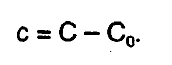
- Within
Figure 6 , it is noted that the value of "h" corresponds to the height of the center of acircle 604 upon which points 606, 608, and 610 can be located. Thepoints circle 604. The value of angle θ can be used to ascertain the linear location (or position) of an object in relationship (or proximity) to the length ofsensor pattern 400. Specifically, the value of height "h" can be determined by using the following relationship:


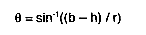

sensor pattern 400 from one of its end points. For example, each degree of angle θ may be equal to a specific distance (e.g., a specific number of millimeters or inches) from one of the end points ofsensor pattern 400. Alternatively, a lookup table may be utilized to ascertain the distance that corresponds to the determined θ. It is noted that the angle θ can provide the location of the center of the object alongsensor pattern 400 while the "h" and the "r" can provide information regarding the size of the object. - One of the advantages of determining the position along the first axis (e.g., X axis) of
sensor pattern 400 in the manner described above is that common-mode noise has no effect on the determination of "r" and θ. - Within
Figure 6 , it is noted that angle θ can alternatively be determined utilizing the following relationships:


- Within
Figure 4 , sensingelements sensor pattern 400 can be embedded within a substrate material (e.g., 404). For example, the distance (or depth) 440 thatsensing element 420 is separated from the capacitivesensing reference surface 402 varies along the length ofsensing element 420. Additionally, the distance (or depth) 450 thatsensing element 430 is separated from the capacitivesensing reference surface 402 varies along the length ofsensing element 430. Note thatsensing element 410 can be implemented in a manner similar to sensingelements - Since sensing
elements reference surface 402 atsection 4D-4D, sensingelements sensing element 410 would have to the object since sensingelement sensing element 410 and the object. -
Figure 5 is a side sectional view of an exemplarycapacitive sensor pattern 500 in accordance with embodiments of the present invention. Specifically,sensor pattern 500 includes sensingelements sensor pattern 500 provides positioning information which can be derived from which sensing element detects an object (e.g., a user's finger, a probe, and the like), and the proportional strength of the signals on sensingelements - Sensing
elements mandrel 520 that provides them a common axis. For example,Figure 5A is a general cross sectional view atsection 5A-5Ashowing sensing element 510 located abovemandrel 520 which is located above sensingelement 530.Figure 5B is a general cross sectional view atsection 5B-5Bshowing sensing element 510 located to the left ofmandrel 520 andsensing element 530 located to the right ofmandrel 520. Additionally,Figure 5C is a general cross sectional view atsection 5C-5Cshowing sensing element 510 located beneathmandrel 520 which is located beneath sensingelement 530.Figure 5D is a general cross sectional view atsection 5D-5Dshowing sensing element 510 located to the right ofmandrel 520 andsensing element 530 located to the left ofmandrel 520.Figure 5E is a general cross sectional view atsection 5E-5Eshowing sensing element 510 located abovemandrel 520 which is located above sensingelement 530. Note that sincesections 5A-5A and 5E-5E show mandrel 520 and sensingelements sensor pattern 500. - Within
Figure 5 , each of sensingelements sensing reference surface 502 along a first axis (e.g., X axis) of thereference surface 502. Note that the length of each of sensingelements sensing elements sensing reference surface 502. Sensingelements - The capacitive coupling associated with
sensing element 510 can vary with the varying distance of portions ofsensing element 510 with respect to the capacitivesensing reference surface 502. Additionally, the capacitive coupling associated with thesensing element 530 can vary with the varying distance of portions ofsensing element 530 with respect to the capacitivesensing reference surface 502. Note that the varying distance of the portions ofsensing element 510 are different from the varying distance of the portions ofsensing element 530. The capacitive coupling.ofsensing element 510 can include a first waveform (e.g., sinusoidal waveform) while the capacitive coupling ofsensing element 530 can include a second waveform (e.g., sinusoidal waveform). Note that every continuous function can be a waveform. The capacitive coupling ofsensing element 510 can include a first phase while the capacitive coupling ofsensing element 530 can include a second phase different from the first phase. For example, the capacitive coupling ofsensing element 510 can be 180 degrees out of phase with the capacitive coupling ofsensing element 530, but is not limited to such. - Within
Figure 5 , each of sensingelements sensing element 510 and the strip of conductive material ofsensing element 530 can be twisted aboutmandrel 520. Therefore, when sensingelement 510 is coupled with sensing circuitry (e.g., 110), it can have varying capacitive coupling to an object proximate to thesensing reference surface 502 as the object moves along the length ofsensing element 510. As such, a different signal strength is provided by sensingelement 510 that is associated with each position or location along its length. It is understood that when sensingelement 530 is coupled with sensing circuitry (e.g., 110), it can operate in a manner similar tosensing element 510, as described above. - Specifically, sensing
elements sensor pattern 500 can be embedded within a substrate material (e.g., 508). The distance (or depth) 506 thatsensing element 510 Is separated from the capacitivesensing reference surface 502 varies along the length ofsensing element 510. Additionally, the distance (or depth) 504 thatsensing element 530 is separated from the capacitivesensing reference surface 502 varies along the length ofsensing element 530. - Within
Figure 5 , since the conductive strips of sensingelements mandrel 520, it is noted that depending on the location of sensingelement 510, it andmandrel 520 can interfere with the capacitive coupling with an object of sensing element 530 (and vice versa). For example, if an object was proximately located toreference surface 502 atsection 5A-5A, sensingelement 510 and mandrel 620 would shield (or limit) the capacitive coupling that sensing element 630 would have to the object since sensingelement 510 andmandrel 520 are located betweensensing element 530 and the object. Alternatively, if the object was proximately located toreference surface 502 atsection 5C-5C,sensing element 530 andmandrel 520 would shield (or limit) the capacitive coupling thatsensing element 510 would have to the object since sensingelement 530 andmandrel 520 are located betweensensing element 510 and the object. -
Figures 7A-7E are described in combination in order to provide a better understanding of an exemplarycapacitive sensor pattern 700a, in accordance with embodiments of the invention. Specifically,Figure 7A is a cross sectional view ofcapacitive sensor pattern 700a in accordance with embodiments of the invention. Additionally,Figures 7B, 7C, 7D, 7E are lengthwise sidesectional views capacitive sensor pattern 700a in accordance with embodiments of the invention. -
Sensor pattern 700a includes sensingelements sensor pattern 700a provides positioning information from a sensor pattern that has substantially parallel traces (or elements) with no crossovers. The positioning information can be derived from which sensing element or elements detect an object (e.g., a user's finger, a probe, and the like) proximate to asensing reference surface 702, and the proportional strength of the signals on sensingelements - Specifically,
capacitive sensor pattern 700a can include an insulatingsubstrate material 704 having a substantially smooth, planar capacitivesensing reference surface 702 where an object (e.g., a user's finger, a probe, and the like) can contact or be proximately located thereto. Thesubstrate 704 includes substantially parallel channels (or grooves) 730, 732, 734, and 736. Along the length of each ofchannels reference surface 702. Additionally,channels groove 730, its distance fromreference surface 702 can be substantially constant. A conductive material can be deposited withinchannels sensing elements elements reference surface 702 as shown inFigures 7B, 7C, and 7D , respectively. When coupled to sensing circuitry (e.g., 110), sensing elements (or traces) 708, 710, and 712 can be used to determine a position of an object relative to a first axis (e.g., X axis) of thesensing reference surface 702 while sensingelement 706 can be used to determine a position of the object relative to a second axis (e.g., Y axis) of thereference surface 702. The second axis may be non-parallel (e.g., substantially perpendicular) to the first axis. - Within
Figures 7A-7E , a conductive material can be deposited withinchannels sensing elements elements substrate 704, wherein the varying depths ofchannels elements sensing elements channels elements - Sensing elements (or traces) 708, 710, and 712 have varying
depths sensing reference surface 702. However, sensing element (or trace) 706 has a substantiallyconstant depth 720 with respect tosensing reference surface 702. In accordance with one embodiment, sensingelements reference surface 702, each of which has a different phase. For example, within the present embodiment, if the waveform shape ofconductive trace 708 is substantially equal to sin θ, then the waveform shape ofconductive trace 710 may be substantially equal to sin (θ + 120 degrees), while the waveform shape ofconductive trace 712 may be substantially equal to sin (θ + 240 degrees). Alternatively, the waveform ofsensing element 710 may be offset (or shifted) from the waveform ofconductive trace 708 by 2π/3 radians while the waveform ofsensing element 712 may be offset (or shifted) from the waveform ofconductive trace 708 by 4π/3 radians. In another embodiment, the waveform ofsensing element 710 can be offset from the waveform ofsensing element 708 by one third of a period while the waveform ofsensing element 712 can be offset from the waveform ofsensing element 708 by two thirds of a period. However, it is understood that the phase and shape of the waveform of sensingelements - Within
Figure 7A-7E , it is understood that the position of the object can be determined using a signal corresponding to sensingelement 708, a signal corresponding to sensingelement 710, and a signal corresponding to sensingelement 712. Thesensing elements sensing elements sensor pattern 700a using signals output by sensingelements sensor pattern 700a can be implemented in a manner similar to that described herein with reference toFigures 4 and6 , but is not limited to such. - Note that
capacitive sensor pattern 700a may have been fabricated utilizing aprocess 1600 ofFigure 16 described below, or by other processes (e.g., that may include machining an insulating material with the desired depth variations). -
Figure 8 is a plan view of an exemplarycapacitive sensor pattern 800 including electrical connections, in accordance with embodiments of the invention. Specifically,sensor pattern 800 includes four repeating sets of sensingelements sensing elements element 706 can have a substantially constant depth (or distance) from the sensing reference surface. Thesensing elements - Within the present embodiment, each of sensing
elements 708 is coupled withelectrical trace 810, each of sensingelements 710 is coupled with trace 820, and each of sensingelements 712 is coupled withtrace 830. However, each of sensingelements 706 is coupled independently withtraces 840.Traces traces 104 and/or 106 ofFigure 1 . When coupled in this manner, thesensor pattern 800 can be utilized to form thesensing region 108. Sensingelements sensor pattern 800. Sensingelements 706 can be used to determine the y-position, or second axis location, of an object (e.g., a finger, a probe, a stylus, etc.) relative tosensor pattern 800. - In another embodiment, each of sensing
elements sensing element 706 may be excluded fromsensor pattern 800. This method of electrically coupling each oftraces sensor pattern 800 independently may involve more than one Application Specific Integrated Circuit (ASIC) if the number of sensing elements is large, whereas the method of interconnecting all sensing elements having the same varying depth and phase, then usingintermediate sensing elements 706 to determine the y-position allows a larger number of sensing elements to be used in conjunction with a single ASIC. - Within
Figure 8 , thesensor pattern 800 can also be implemented withguard trace 850 at the "top" andguard trace 852 at the "bottom" ofsensor pattern 800, thereby enabling the "edge" sensing elements located near them to operate in a manner similar to those sensing elements more centrally located within thesensor pattern 800. The guard traces 850 and 852 may be electrically driven, grounded and/or held at a substantially fixed or constant potential in accordance with embodiments of the present invention. - For example, guard traces 850 and 852 of
Figure 8 may be coupled to ground viatraces traces traces - Noted that one or more guard traces (or grounded or fixed potential traces) similar to guard traces 850 and 852 can also be included as part of or with any sensing pattern described herein.
- Although
sensor pattern 800 ofFigure 8 indicates using repeated sets of three sensing elements to determine the x-position (e.g., first axis) of an object relative tosensor pattern 800, it should be understood that a different number of sensing elements may be employed, using an appropriate mathematical relationship, to discern the x-position of an object. -
Figure 9 is a plan view of anexemplary sensor pattern 900 in accordance with embodiments of the invention.Sensor pattern 900 includes six repeated patterns of sensingelements elements sensing elements elements sensor pattern 900 can provide two-dimensional positioning information that has substantially parallel traces (or sensing elements) with no crossovers. Thesensor pattern 900 can be utilized in any manner similar to that described herein, but is not limited to such. - It is noted that the six repeated patterns of sensing
elements elements sensor pattern 800 ofFigure 8 , described herein. -
Figures 10A and 10B are side sectional views of an exemplarycapacitive sensor pattern 1000 Specifically,sensor pattern 1000 Includes sensingelements sensor pattern 1000 provides positioning information which can be derived from which sensing element detects an object (e.g., a user's finger, a probe, and the like), and the proportional strength of the signals onsensing elements - Each of
sensing elements sensing reference surface 1002 along a first axis (e.g., X axis) of thereference surface 1002. Specifically, the capacitive coupling ofsensing element 1020 can vary with variations in dielectric constant between the capacitivesensing reference surface 1002 and portions ofsensing element 1020. Furthermore, the capacitive coupling ofsensing element 1022 can vary with variations in dielectric constant between the capacitivesensing reference surface 1002 and portions ofsensing element 1022. It is appreciated that the variations in the dielectric constant forsensing element 1020 can be different from the variations in the dielectric constant forsensing element 1022. Therefore, sensingelements sensing reference surface 1002, while each can be configured to have varying capacitive coupling to an object proximate tosensing reference surface 1002. - Within
Figures 10A and 10B , the length of each ofsensing elements sensing elements sensing reference surface 1002. Note thatsensing elements - Each of
sensing elements Figure 10A ,sensing element 1020 is disposed above asubstrate 1008, while adielectric material 1006 is disposed abovesensing element 1020, and adielectric material 1004 is disposed abovedielectric material 1006. Note that the upper surface ofdielectric material 1006 increasingly slopes away from capacitivesensing reference surface 1002. Given thatdielectric material 1004 has a lower dielectric constant thandielectric material 1006 andsensing element 1020 is coupled to sensing circuitry (e.g., 110),sensing element 1020 can have a stronger capacitive coupling to an object proximate to the left-hand side of capacitivesensing reference surface 1002 than when proximate to its right-hand side. Therefore, when sensingelement 1020 is coupled with sensing circuitry (e.g., 110), it can have varying capacitive coupling to an object proximate to thesensing reference surface 1002 as the object moves along the length ofsensing element 1020. As such, a different signal strength is provided bysensing element 1020 that is associated with each position or location along its length. - Within
Figure 10B ,sensing element 1022 is disposed abovesubstrate 1008, while adielectric material 1010 is disposed abovesensing element 1022, and adielectric material 1012 is disposed abovedielectric material 1010. Note that the upper surface ofdielectric material 1010 increasingly slopes away from capacitivesensing reference surface 1002. Given thatdielectric material 1010 has a lower dielectric constant thandielectric material 1012 andsensing element 1022 is coupled to sensing circuitry (e.g., 110),sensing element 1022 can have a stronger capacitive coupling to an object proximate to the left-hand side of capacitivesensing reference surface 1002 than when proximate to its right-hand side. Therefore, when sensingelement 1022 is coupled with sensing circuitry (e.g., 110), it can have varying capacitive coupling to an object proximate to thesensing reference surface 1002 as the object moves along the length ofsensing element 1022. As such, a different signal strength is provided bysensing element 1022 that is associated with each position or location along its length. - Within
Figures 10A and 10B , note thatdielectric materials elements reference surface 1002 travels along the length ofsensing elements sensing reference surface 1002. -
Figure 11 is a plan view of an exemplary loopcapacitive sensor pattern 1100 in accordance with embodiments of the invention. Specifically,sensor pattern 1100 includes three sets of concentric loop patterns ofsensing elements sensor pattern 1100 can be utilized as part of a single layer capacitive sensor apparatus (e.g., 100), such as but not limited to, a touch pad. When electrically coupled,sensor pattern 1100 can provide continuous two-dimensional positioning information that has sensing elements with varying depth and no crossovers. Thesensor pattern 1100 can be utilized in any manner similar to that described herein, but is not limited to such. - Specifically, each of the
sensing elements sensing elements origin 1102 which can be located anywhere associated withsensor pattern 1100. Thesensing elements sensing elements - Within
Figure 11 , thesensing elements - Each of the sensing elements (e.g., 708a, 710a, and 712a) of the
sensor pattern 1100 can be individually coupled with sensing circuitry (e.g., 110) utilizing conductive coupling traces (e.g., 104 and/or 106). When coupled in this manner, thesensor pattern 1100 can be utilized to form a sensing region (e.g., 108). Furthermore, when coupled in this manner,sensor pattern 1100 can provide positioning information along the angular position φ and the radial position "R". - Alternatively, all similar sensing elements (e.g., 712a) of
sensor pattern 1100 can be coupled together as shown inFigure 8 and coupled with sensing circuitry (e.g., 110) utilizing a conductive coupling trace (e.g., 104 or 106). When coupled in this manner, thesensor pattern 1100 can provide positioning information to the sensing circuitry corresponding to the angular position φ, but not of the radial position "R". It is understood that the radial position "R" can be determined in any manner similar to the way the second axis position can be determined, as described herein. -
Sensor pattern 1100 can be implemented with a greater or lesser number of sensing elements than shown within the present embodiment. For example,sensor pattern 1100 can be implemented with a single set ofsensing elements sensor pattern 1100 can be implemented with multiple sets ofsensing elements Sensor pattern 1100 and its sensing elements can be implemented in any manner similar to that described herein, but is not limited to such. - Within
Figure 11 , each set of the sensing elements (e.g., 708a, 710a, and 712a) ofsensor pattern 1100 can operate in any manner similar to that described herein in order to provide the positioning information corresponding to the angular position φ of an object (e.g., a user's finger, a probe, a stylus, and the like) in relation tosensor pattern 1100. Thesensing elements Figure 6 . Noted that once the phase angle θ has been determined, it may be converted into a geometric position angle φ relative to theorigin 1102. In this manner, the angular position φ of an object is determined relative tosensor pattern 1100. -
Figure 12 illustrates an exemplary loopcapacitive sensor pattern 1200 in accordance with embodiments of the present invention. Specifically,sensor pattern 1200 Includes three sets of concentric loop patterns of sensingelements sensing elements element 706b can have a substantially constant depth from the reference surface. Thesensing elements Sensor pattern 1200 can be utilized as part of a single layer capacitive sensor apparatus (e.g., 100), such as, but not limited to, a touch pad. When electrically coupled,sensor pattern 1200 can provide continuous two-dimensional positioning information that has sensing elements with varying depth and no crossovers. Thesensor pattern 1200 can be utilized in any manner similar to that described herein, but is not limited to such. - Specifically, sensing
elements sensing elements origin 1202 which can be located anywhere associated withsensor pattern 1200. Thesensing elements sensing elements - Within
Figure 12 , thesensing elements sensor pattern 1200 can be coupled together as shown inFigure 8 and coupled with sensing circuitry (e.g., 110) utilizing a conductive coupling trace (e.g., 104 or 106). When coupled in this manner, thesensor pattern 1200 can provide positioning information to the sensing circuitry corresponding to the angular position φ, but not of the radial position "R". It is understood that the radial position "R" can be determined fromsensors 706b in any manner similar to the way the second axis position can be determined, as described herein. -
Sensor pattern 1200 can be implemented with a greater or lesser number of sensing elements than shown within the present embodiment. For example,sensor pattern 1200 can be implemented with a single set of sensingelements sensor pattern 1200 can be implemented with multiple sets of sensingelements Sensor pattern 1200 and its sensing elements can be Implemented In any manner similar to that described herein, but is not limited to such. - Within
Figure 12 , each set of the varyingdepth sensing elements sensor pattern 1200 can operate in any manner similar to that described herein in order to provide the positioning information corresponding to the angular position φ of an object (e.g., a user's finger, a probe, a stylus, and the like) in relation tosensor pattern 1200. For example, each set of the signals associated with the set of varyingdepth sensing elements Figure 6 . Noted that once the phase angle θ has been determined, it may be converted into a geometric position angle φ relative to theorigin 1202. In this manner, the angular position φ of an object is determined relative tosensor pattern 1200. -
Figure 13 is a plan view of an exemplary loopcapacitive sensor pattern 1300 in accordance with embodiments of the invention. Specifically,sensor pattern 1300 includes three sets of concentric loop patterns of sensingelements sensing elements sensing elements sensing elements sensor pattern 1300 can provide continuous two-dimensional positioning information that has sensing elements with varying depth and no crossovers. Thesensor pattern 1300 can be utilized in any manner similar to that described herein, but is not limited to such. - Note that
sensor pattern 1300 can operate In any manner similar tosensor pattern 1100 ofFigure 11 . Thesensor pattern 1300 can be Implemented with a greater or lesser number of sensing elements than shown within the present embodiment.Sensor pattern 1300 and its sensing elements can be implemented in any manner similar to that described herein, but is not limited to such. -
Figure 14 is a plan view of an exemplary loopcapacitive sensor pattern 1400 in accordance with embodiments of the invention. Specifically,sensor pattern 1400 includes two sets of concentric loop patterns ofsensing elements sensing elements element 706d can have a substantially constant depth or distance from the reference surface. Thesensing elements sensing elements sensor pattern 1400 can provide continuous two-dimensional positioning information that has sensing elements with varying depth and no crossovers. Thesensor pattern 1400 can be utilized in any manner similar to that described herein, but is not limited to such. - It is appreciated that
sensor pattern 1400 can operate in any manner similar to sensor patterns 1100 (Figure 11 ) and/or 1200 (Figure 12 ). Thesensor pattern 1400 can be Implemented with a greater or lesser number of sensing elements than shown within the present embodiment.Sensor pattern 1400 and its sensing elements can be implemented in any manner similar to that described herein, but is not limited to such. -
Figure 15 is a plan view of an exemplary "fishbone"capacitive sensor pattern 1500 in accordance with embodiments of the invention. Specifically,sensor pattern 1500 includes a set ofsensing elements sensing elements sensor pattern 1500 can provide two-dimensional positioning information that has substantially parallel traces (or sensing elements) with no crossovers. Thesensor pattern 1500 can be utilized in any manner similar to that described herein with reference toFigures 7A-7E ,8 , and9 , but is not limited to such. Moreover,sensor pattern 1500 can be utilized in any manner similar to that described herein, but is not limited to such. - Specifically,
sensing element 708e can include a plurality ofextensions 1502 that are substantially parallel to each other and are substantially perpendicular to a first axis ofsensing element 708e. Thesensing element 710e can include a plurality ofextensions 1504 that are substantially parallel to each other and are substantially perpendicular to the first axis of sensing element 71 0e. Thesensing element 712e can include a plurality ofextensions 1506 that are substantially parallel to each other and are substantially perpendicular to the first axis ofsensing element 712e. - Within
Figure 15 , the plurality ofextensions 1502 ofsensing element 708e can be interdigitated with the plurality ofextensions 1504 ofsensing element 710e. Moreover, the plurality ofextensions 1506 ofsensing element 712e can be interdigitated with the plurality ofextensions 1504 ofsensing element 710e. -
Sensing elements sensor pattern 1500 along the first axis of a two-dimensional space. Furthermore, a repeated set ofsensing elements sensor pattern 1500 along the first axis and a second axis of the two-dimensional space, wherein the second axis is substantially non-parallel (or substantially perpendicular) to the first axis. - Within
Figure 15 ,sensor pattern 1500 can operate in any manner similar tosensor patterns 700a-700e ofFigures 7A-E . Additionally, thesensor pattern 1500 can be implemented with a greater or lesser number of sensing elements than shown within the present embodiment.Sensor pattern 1500 and its sensing elements can be implemented in any manner similar to that described herein, but is not limited to such. -
Figure 16 is a flowchart of amethod 1600 for establishing a position-varying capacitive coupling between a conductive object proximate to a capacitive sensing reference surface and a conductive trace in accordance with embodiments of the invention. Although specific operations are disclosed inmethod 1600, such operations are exemplary. That is,method 1600 may not include all of the operations illustrated byFigure 16 . Alternatively,method 1600 may include various other operations and/or variations of the operations shown byFigure 16 . - Specifically, a plurality of channel patterns can be provided (or formed) in a substrate. Note that the channel patterns varying in depth. A conductive material can be deposited onto the channel patterns to form a first sensing element and second sensing element. The first sensing element and second sensing element can be conductive and lie substantially along a first orientation. Furthermore, each of the first sensing element and second sensing element can be configured to provide information corresponding to a first location along the first orientation.
- At
operation 1610 ofFigure 16 , a plurality of channel (or groove) patterns having varying depth can be provided (or formed) in a substrate. It is understood that the substrate can be implemented in a wide variety of ways. For example, the substrate can be implemented to include, but is not limited to, a plastic or a crystalline material. Additionally, the substrate can be implemented as a component of an information display device or a portable computing device. For example, the substrate can be implemented as a part of a casing or front cover of an information display device or portable computing device. The channel patterns can include waveforms or portions of waveforms. For example, the channel patterns can Include one or more sinusoidal waveforms. Alternatively, the channel patterns can include one or more portions of a sinusoidal waveform. - At
operation 1620, a conductive material can be deposited onto the channel (or groove) patterns to form a first sensing element and second sensing element that are conductive and lie substantially along a first orientation. Note that more than two sensing elements can be formed atoperation 1620. Each of the first sensing element and second sensing element can be configured to provide information corresponding to a first location along the first orientation. Note that the first orientation can be implemented in diverse ways. For example, the first orientation can be substantially linear. Alternatively, the first orientation can be non-linear. The first and second sensing elements can be implemented in a wide variety of ways. For example, the first sensing element can include a first waveform while the second sensing element can Include a second waveform. Additional, the first waveform and the second waveform can be different or similar. The first waveform and the second waveform can each include one or more sinusoidal waveforms or a portion of a sinusoidal waveform. Moreover, the first waveform and the second waveform can each have a different phase. It is understood that the first sensing element and second sensing element can each form at least a portion of a loop or a curve: - At
operation 1630 ofFigure 16 , the first sensing element can be backfilled with a material. Note that the second sensing element may also be backfilled with a material atoperation 1630. Note that the backfilling material can be implemented in a wide variety of ways. For example, the material can be implemented as, but not limited to, the material of which the substrate is formed, insulting material, and/or electrical shielding material. This optional backfilling material can provide physical protection to the one or more sensing elements. Additionally, the backfilling material can provide electrical shielding thereby causing the one or more sensing elements to measure capacitance on a desired reference sensing surface of the substrate, instead of on both sides of the substrate. Moreover, the backfilling material can provide a smooth back surface on the substrate that may be desirable in some circumstances. - By fabricating the capacitive sensor pattern in the manner shown in
Figure 16 , failure rates can be reduced since only one layer of conductive material is utilized, and there are no crossovers in the sensing elements. In addition, the capacitive sensor pattern may be manufactured very inexpensively by molding the channel patterns into the case of a laptop computer or other electronic device and depositing (or printing or spraying) the conductive material onto the channel patterns. - Note that sensor patterns in accordance with embodiments of the invention do not induce signal to noise ratio concerns.
- The foregoing descriptions of specific embodiments of the present invention have been presented for purposes of illustration and description. They are not intended to be exhaustive or to limit the Invention to the precise forms disclosed, and obviously many modifications and variations are possible In light of the above teaching. The embodiments were chosen and described in order to best explain the principles of the invention and its practical application, to thereby enable others skilled in the art to best utilize the invention and various embodiments with various modifications as are suited to the particular use contemplated. It is intended that the scope of the invention be defined by the Claims appended hereto.
Claims (31)
- A capacitive sensing device for establishing a position-varying capacitive coupling between a conductive object proximate to a capacitive sensing reference surface (202; 302; 402; 502; 702) and a conductive trace, said device being characterized in that it comprises:a plurality of channel (730, 732) patterns in a substrate (204; 304; 404; 508; 704), said channel patterns (730, 732) varying in depth; anda conductive material deposited on said channel patterns to form a first sensing element (206; 310; 410; 510; 708) and second sensing element (208; 320; 420; 530; 710),wherein said first sensing element (206; 310; 410; 510; 708) and second sensing element(208; 320; 420; 530; 710) are conductive and are substantially along a first orientation andeach of said first sensing element (206; 310; 410; 510; 708) and second sensing element (208; 320; 420; 530; 710) is configured to provide information corresponding to a first location along said first orientation.
- The capacitive sensing device as recited in Claim 1, wherein said first orientation is substantially linear.
- The capacitive sensing device as recited in Claim 1, wherein said first orientation is non linear.
- The capacitive sensing device as recited in Claim 1, wherein: said first sensing element (206; 310; 410; 510; 708) comprises a first waveform; and said second sensing element (208; 320; 420; 530; 710) comprises a second waveform.
- The capacitive sensing device as recited in Claim 1, wherein said first sensing element (206; 310; 410; 510; 708) and said second sensing element (208; 320; 420; 530; 710) each forms at least a portion of a loop.
- The capacitive sensing device of claim 1, wherein:the first sensing element (410; 708) has varying depth relative to the capacitive sensing reference surface (402; 702);the second sensing element (420; 710) is substantially parallel to said first sensing element, and has varying depth relative to said capacitive sensing reference surface (402; 702); the device further comprising:a third sensing element (430; 710) substantially parallel to said first sensing element (410; 708), and having varying depth relative to said capacitive sensing reference surface (402; 702),wherein said first sensing element (410; 708), second sensing element (420; 710), and third sensing element (430; 712) are configured to provide information corresponding to a position of an object proximate to said capacitive sensing reference surface (402; 702) along a first axis of said capacitive sensing reference surface (402; 702).
- The capacitive sensing device of Claim 6, wherein:portions of said first sensing element (410; 708) are configured to have a capacitive coupling with respect to said object wherein said capacitive coupling varies along said first axis;portions of said second sensing element (420; 710) are configured to have a capacitive coupling with respect to said object wherein said capacitive coupling varies along said first axis; andportions of said third sensing element (430; 712) are configured to have a capacitive coupling with respect to said object wherein said capacitive coupling varies along said first axis.
- The capacitive sensing device of claim 6, wherein the first (410; 708), second (420; 710) and third sensing elements (430; 712) each include a waveform, each of which having a different phase.
- The capacitive sensing device of Claim 6, wherein:said first sensing element (410; 708) has varying depth comprising a waveform;said second sensing element (420; 710) has varying depth comprising a waveform that is offset from said waveform of said first sensing element by one third of a period; andsaid third sensing element (430; 712) has varying depth comprising a waveform that is offset from said waveform of said first sensing element by two thirds of a period.
- The capacitive sensing device of Claim 6, wherein said position is determined using a signal corresponding to said first sensing element (410; 708), a signal corresponding to said second sensing element (420; 710), and a signal corresponding to said third sensing element (430; 712).
- The capacitive sensing device of Claim 10, wherein said position is determined using a trigonometric function.
- The capacitive sensing device of Claim 6, wherein said first sensing element (410; 708), said second sensing element (420; 710), and said third sensing element (430; 712) each comprises a conductive trace.
- The capacitive sensing device of Claim 12, wherein each said conductive trace is disposed above a substrate (704), wherein a side of said substrate (704) comprises channels (730, 732, 734) of varying depths, said varying depths defining a unique depth profile for each of said first (708), second (710), and third (712) sensing elements.
- The capacitive sensing device of Claim 6, wherein at least one of said first sensing element (410; 708), second sensing element (420; 710), and third sensing element (430; 712) is used for determining a second position along a second axis substantially perpendicular to said first axis.
- The capacitive sensing device of Claim 6, wherein:said first sensing element (410; 708) has varying depth comprising a first sinusoidal waveform;said second sensing element (420; 710) has varying depth comprising a second sinusoidal waveform offset from said first sinusoidal waveform; andsaid third sensing element (430; 712) has varying depth comprising a third sinusoidal waveform offset from said first sinusoidal waveform and said second sinusoidal waveform.
- The capacitive sensing device of Claim 6, further comprising:a fourth sensing element (706) utilized for determining a second position along a second axis that is non-parallel to said first axis.
- The capacitive sensing device of Claim 6, further comprising:a fourth sensing element having varying depth;a fifth sensing element having varying depth;a sixth sensing element having varying depth, wherein said fourth, fifth, and sixth sensing elements are substantially parallel to said first sensing element, and are configured for determining said position along said first axis.
- The capacitive sensing device of Claim 17, wherein at least one of said first, second, third, fourth, fifth, and sixth sensing elements is configured for determining a second position along a second axis, said second axis not parallel to said first axis.
- The capacitive sensing device of Claim 6, wherein said first (410; 708), second (420; 710), and third (430; 712) sensing elements are utilized as part of a capacitive touch pad device.
- A portable electronic device comprising:a capacitive sensing device according to claim 6;a processor coupled with said capacitive sensing device, wherein said capacitive sensing devicecomprises:a first sensing element (410; 708) having varying depth comprising a sine (θ) waveform;a second sensing element (420; 710) having varying depth comprising a sine (θ) waveform shifted by 2π/3 radians from said sine (θ) waveform of said first sensing element; anda third sensing element (430; 712) having varying depth comprising a sine (θ) waveform shifted from said sine (θ) waveform of said first sensing element by 4π/3 radians.
- The portable electronic device of Claim 20, wherein at least one of said first sensing element (410; 708), second sensing element (420; 710), and third sensing element (430; 712) is used for determining a second position along a second axis not parallel to said first axis.
- The portable electronic device of Claim 20, wherein said first location along said first axis is determined using signals from said first sensing element (410; 708), said second sensing element (420; 710), and said third sensing element (430; 712).
- The portable electronic device of Claim 20 wherein said first location along said first axis is determined using a trigonometric function.
- The portable electronic device of Claim 20, further comprising: a fourth sensing element (706) utilized to determine a second location along a second axis that is substantially perpendicular to said first axis.
- A method for establishing a position-varying capacitive coupling between a conductive object proximate to a capacitive sensing reference surface (202; 302; 402; 502; 702) and a conductive trace, said method being characterized in that it comprises:providing a plurality of channel (730, 732) patterns in a substrate (204; 304; 404; 508; 704), said channel (730, 732) patterns varying in depth; anddepositing a conductive material onto said channel patterns to form a first sensing element (206; 310; 410; 510; 708) and second sensing element (208; 320; 420; 530; 710),wherein said first sensing element (206; 310; 410; 510; 708) and second sensing element (208; 320; 420; 530; 710) are conductive and are substantially along a first orientation andeach of said first sensing element (206; 310; 410; 510; 708) and second sensing element (208; 320; 420; 530; 710) is configured to provide information corresponding to a first location along said first orientation.
- The method as recited in Claim 25, wherein said first orientation is substantially linear.
- The method as recited in Claim 25, wherein said first orientation is non linear.
- The method as recited in Claim 25, wherein: said first sensing element (206; 310; 410; 510; 708) comprises a first waveform; and said second sensing element (208; 320; 420; 530; 710) comprises a second waveform.
- The method as recited in Claim 25, further comprising: backfilling said first sensing element (206; 310; 410; 510; 708) with a material.
- The method as recited in Claim 25, wherein said first sensing element (206; 310; 410; 510; 708) and said second sensing element (208; 320; 420; 530; 710) each forms at least a portion of a loop.
- The method as recited in claim 25, comprising depositing a conductive material onto said channel patterns to form a third conductive sensing element (430; 712) substantially along the first orientation, configured to provide information corresponding to a first location along said first orientation, wherein:the first sensing element (410; 708) has varying depth comprising a sine (θ) waveform;the second sensing element (420; 710) has varying depth comprising a sine (θ) waveform shifted by 2π/3 radians from said sine (θ) waveform of said first sensing element; andthe third sensing element (430; 712) has varying depth comprising a sine (θ) waveform shifted from said sine (θ) waveform of said first sensing element by 4n/3 radians.
Applications Claiming Priority (2)
| Application Number | Priority Date | Filing Date | Title |
|---|---|---|---|
| US10/922,574 US7737953B2 (en) | 2004-08-19 | 2004-08-19 | Capacitive sensing apparatus having varying depth sensing elements |
| PCT/US2005/024206 WO2006023147A2 (en) | 2004-08-19 | 2005-07-07 | Capacitive sensing apparatus having varying depth sensing elements |
Publications (2)
| Publication Number | Publication Date |
|---|---|
| EP1782174A2 EP1782174A2 (en) | 2007-05-09 |
| EP1782174B1 true EP1782174B1 (en) | 2012-11-28 |
Family
ID=35266998
Family Applications (1)
| Application Number | Title | Priority Date | Filing Date |
|---|---|---|---|
| EP05764532A Not-in-force EP1782174B1 (en) | 2004-08-19 | 2005-07-07 | Capacitive sensing apparatus having varying depth sensing elements |
Country Status (6)
| Country | Link |
|---|---|
| US (2) | US7737953B2 (en) |
| EP (1) | EP1782174B1 (en) |
| JP (1) | JP4956430B2 (en) |
| KR (1) | KR101129665B1 (en) |
| CN (1) | CN101006416B (en) |
| WO (1) | WO2006023147A2 (en) |
Families Citing this family (173)
| Publication number | Priority date | Publication date | Assignee | Title |
|---|---|---|---|---|
| JP4681795B2 (en) * | 2001-05-18 | 2011-05-11 | デカ・プロダクツ・リミテッド・パートナーシップ | Fluid pump infusion set |
| US8034026B2 (en) * | 2001-05-18 | 2011-10-11 | Deka Products Limited Partnership | Infusion pump assembly |
| US7345671B2 (en) * | 2001-10-22 | 2008-03-18 | Apple Inc. | Method and apparatus for use of rotational user inputs |
| US20070085841A1 (en) * | 2001-10-22 | 2007-04-19 | Apple Computer, Inc. | Method and apparatus for accelerated scrolling |
| US7312785B2 (en) * | 2001-10-22 | 2007-12-25 | Apple Inc. | Method and apparatus for accelerated scrolling |
| US7333092B2 (en) * | 2002-02-25 | 2008-02-19 | Apple Computer, Inc. | Touch pad for handheld device |
| US20070152977A1 (en) * | 2005-12-30 | 2007-07-05 | Apple Computer, Inc. | Illuminated touchpad |
| US20060181517A1 (en) * | 2005-02-11 | 2006-08-17 | Apple Computer, Inc. | Display actuator |
| US7499040B2 (en) * | 2003-08-18 | 2009-03-03 | Apple Inc. | Movable touch pad with added functionality |
| US7495659B2 (en) * | 2003-11-25 | 2009-02-24 | Apple Inc. | Touch pad for handheld device |
| US8059099B2 (en) * | 2006-06-02 | 2011-11-15 | Apple Inc. | Techniques for interactive input to portable electronic devices |
| EP1779228B1 (en) * | 2004-08-16 | 2012-04-11 | Apple Inc. | A method of increasing the spatial resolution of touch sensitive devices |
| TWI273497B (en) * | 2004-12-14 | 2007-02-11 | Elan Microelectronics Corp | Dual-axis unequal-interval interlacing-type sensing-scan capacitance-type touch panel |
| TWI274529B (en) * | 2005-03-11 | 2007-02-21 | Elan Microelectronics Corp | Touch board with single-layer PCB structure |
| US7880729B2 (en) * | 2005-10-11 | 2011-02-01 | Apple Inc. | Center button isolation ring |
| US7683891B2 (en) * | 2005-12-22 | 2010-03-23 | Synaptics Incorporated | Equalizing reference surface capacitance with uneven thickness |
| US20070152983A1 (en) * | 2005-12-30 | 2007-07-05 | Apple Computer, Inc. | Touch pad with symbols based on mode |
| WO2007095093A2 (en) | 2006-02-09 | 2007-08-23 | Deka Products Limited Partnership | Pumping fluid delivery systems and methods using force application assembly |
| US11364335B2 (en) | 2006-02-09 | 2022-06-21 | Deka Products Limited Partnership | Apparatus, system and method for fluid delivery |
| US11497846B2 (en) | 2006-02-09 | 2022-11-15 | Deka Products Limited Partnership | Patch-sized fluid delivery systems and methods |
| US11027058B2 (en) | 2006-02-09 | 2021-06-08 | Deka Products Limited Partnership | Infusion pump assembly |
| US11478623B2 (en) | 2006-02-09 | 2022-10-25 | Deka Products Limited Partnership | Infusion pump assembly |
| US9360967B2 (en) * | 2006-07-06 | 2016-06-07 | Apple Inc. | Mutual capacitance touch sensing device |
| US8022935B2 (en) | 2006-07-06 | 2011-09-20 | Apple Inc. | Capacitance sensing electrode with integrated I/O mechanism |
| US8743060B2 (en) | 2006-07-06 | 2014-06-03 | Apple Inc. | Mutual capacitance touch sensing device |
| US7688080B2 (en) * | 2006-07-17 | 2010-03-30 | Synaptics Incorporated | Variably dimensioned capacitance sensor elements |
| US7795553B2 (en) | 2006-09-11 | 2010-09-14 | Apple Inc. | Hybrid button |
| US8274479B2 (en) * | 2006-10-11 | 2012-09-25 | Apple Inc. | Gimballed scroll wheel |
| US20080088597A1 (en) * | 2006-10-11 | 2008-04-17 | Apple Inc. | Sensor configurations in a user input device |
| US20080088600A1 (en) * | 2006-10-11 | 2008-04-17 | Apple Inc. | Method and apparatus for implementing multiple push buttons in a user input device |
| US8482530B2 (en) * | 2006-11-13 | 2013-07-09 | Apple Inc. | Method of capacitively sensing finger position |
| AU2007328233B2 (en) | 2006-12-04 | 2012-09-13 | Deka Products Limited Partnership | Medical device including a slider assembly |
| US20080136787A1 (en) * | 2006-12-11 | 2008-06-12 | I-Hau Yeh | Touchpad having Single Layer Layout |
| US8243043B2 (en) * | 2007-03-29 | 2012-08-14 | Cirque Corporation | Driven shield for capacitive touchpads |
| US8063330B2 (en) * | 2007-06-22 | 2011-11-22 | Nokia Corporation | Uniform threshold for capacitive sensing |
| US20090040191A1 (en) * | 2007-08-08 | 2009-02-12 | Synaptics Incorporated | Capacitive touch sensor with conductive trace lines in bonding region |
| US20090045823A1 (en) * | 2007-08-13 | 2009-02-19 | Winbond Electronics Corporation | Power efficient capacitive detection |
| WO2009032898A2 (en) * | 2007-09-04 | 2009-03-12 | Apple Inc. | Compact input device |
| US20090058801A1 (en) * | 2007-09-04 | 2009-03-05 | Apple Inc. | Fluid motion user interface control |
| US8683378B2 (en) * | 2007-09-04 | 2014-03-25 | Apple Inc. | Scrolling techniques for user interfaces |
| US20090073130A1 (en) * | 2007-09-17 | 2009-03-19 | Apple Inc. | Device having cover with integrally formed sensor |
| US8633915B2 (en) | 2007-10-04 | 2014-01-21 | Apple Inc. | Single-layer touch-sensitive display |
| US8416198B2 (en) | 2007-12-03 | 2013-04-09 | Apple Inc. | Multi-dimensional scroll wheel |
| US8881774B2 (en) | 2007-12-31 | 2014-11-11 | Deka Research & Development Corp. | Apparatus, system and method for fluid delivery |
| US10080704B2 (en) | 2007-12-31 | 2018-09-25 | Deka Products Limited Partnership | Apparatus, system and method for fluid delivery |
| EP3679969A3 (en) | 2007-12-31 | 2020-09-30 | DEKA Products Limited Partnership | Infusion pump assembly |
| US10188787B2 (en) | 2007-12-31 | 2019-01-29 | Deka Products Limited Partnership | Apparatus, system and method for fluid delivery |
| US8900188B2 (en) | 2007-12-31 | 2014-12-02 | Deka Products Limited Partnership | Split ring resonator antenna adapted for use in wirelessly controlled medical device |
| CN104874047B (en) | 2007-12-31 | 2019-05-28 | 德卡产品有限公司 | It is transfused pump assembly |
| US9456955B2 (en) | 2007-12-31 | 2016-10-04 | Deka Products Limited Partnership | Apparatus, system and method for fluid delivery |
| US20090174676A1 (en) | 2008-01-04 | 2009-07-09 | Apple Inc. | Motion component dominance factors for motion locking of touch sensor data |
| US8125461B2 (en) * | 2008-01-11 | 2012-02-28 | Apple Inc. | Dynamic input graphic display |
| US8820133B2 (en) * | 2008-02-01 | 2014-09-02 | Apple Inc. | Co-extruded materials and methods |
| EP2260367A4 (en) * | 2008-02-28 | 2014-05-14 | 3M Innovative Properties Co | Touch screen sensor with low visibility conductors |
| US8119937B2 (en) * | 2008-03-10 | 2012-02-21 | Young Fast Optoelectronics Co., Ltd. | Capacitive touch panel |
| US9454256B2 (en) | 2008-03-14 | 2016-09-27 | Apple Inc. | Sensor configurations of an input device that are switchable based on mode |
| TW201008118A (en) * | 2008-04-10 | 2010-02-16 | Atmel Corp | Capacitive touch screen with noise suppression |
| US8487898B2 (en) * | 2008-04-25 | 2013-07-16 | Apple Inc. | Ground guard for capacitive sensing |
| US8576193B2 (en) * | 2008-04-25 | 2013-11-05 | Apple Inc. | Brick layout and stackup for a touch screen |
| US20100058251A1 (en) * | 2008-08-27 | 2010-03-04 | Apple Inc. | Omnidirectional gesture detection |
| US20100060568A1 (en) * | 2008-09-05 | 2010-03-11 | Apple Inc. | Curved surface input device with normalized capacitive sensing |
| US20100059294A1 (en) * | 2008-09-08 | 2010-03-11 | Apple Inc. | Bandwidth enhancement for a touch sensor panel |
| EP3881874A1 (en) | 2008-09-15 | 2021-09-22 | DEKA Products Limited Partnership | Systems and methods for fluid delivery |
| US8816967B2 (en) * | 2008-09-25 | 2014-08-26 | Apple Inc. | Capacitive sensor having electrodes arranged on the substrate and the flex circuit |
| US8262616B2 (en) * | 2008-10-10 | 2012-09-11 | Deka Products Limited Partnership | Infusion pump assembly |
| US8066672B2 (en) | 2008-10-10 | 2011-11-29 | Deka Products Limited Partnership | Infusion pump assembly with a backup power supply |
| US8267892B2 (en) | 2008-10-10 | 2012-09-18 | Deka Products Limited Partnership | Multi-language / multi-processor infusion pump assembly |
| US8223028B2 (en) | 2008-10-10 | 2012-07-17 | Deka Products Limited Partnership | Occlusion detection system and method |
| US8016789B2 (en) * | 2008-10-10 | 2011-09-13 | Deka Products Limited Partnership | Pump assembly with a removable cover assembly |
| US8708376B2 (en) * | 2008-10-10 | 2014-04-29 | Deka Products Limited Partnership | Medium connector |
| US9180245B2 (en) | 2008-10-10 | 2015-11-10 | Deka Products Limited Partnership | System and method for administering an infusible fluid |
| US8243075B2 (en) * | 2008-10-14 | 2012-08-14 | Autodesk, Inc. | Graphics processing unit accelerated dynamic radial tessellation |
| US8395590B2 (en) * | 2008-12-17 | 2013-03-12 | Apple Inc. | Integrated contact switch and touch sensor elements |
| US8922521B2 (en) | 2009-02-02 | 2014-12-30 | Apple Inc. | Switching circuitry for touch sensitive display |
| US9261997B2 (en) * | 2009-02-02 | 2016-02-16 | Apple Inc. | Touch regions in diamond configuration |
| KR101035967B1 (en) * | 2009-04-01 | 2011-05-23 | 주식회사 애트랩 | Touch sensor device |
| US8593410B2 (en) | 2009-04-10 | 2013-11-26 | Apple Inc. | Touch sensor panel design |
| US8154529B2 (en) * | 2009-05-14 | 2012-04-10 | Atmel Corporation | Two-dimensional touch sensors |
| US9354751B2 (en) * | 2009-05-15 | 2016-05-31 | Apple Inc. | Input device with optimized capacitive sensing |
| US8957874B2 (en) * | 2009-06-29 | 2015-02-17 | Apple Inc. | Touch sensor panel design |
| JP5252454B2 (en) * | 2009-06-30 | 2013-07-31 | 株式会社ジャパンディスプレイウェスト | Contact detection device and display device having touch sensor function |
| US8872771B2 (en) * | 2009-07-07 | 2014-10-28 | Apple Inc. | Touch sensing device having conductive nodes |
| CA2768011C (en) | 2009-07-15 | 2018-07-24 | Deka Products Limited Partnership | Apparatus, systems and methods for an infusion pump assembly |
| TWI428809B (en) * | 2009-08-28 | 2014-03-01 | Elan Microelectronics Corp | Two - dimensional structure of the capacitive touchpad positioning method |
| JP2013504819A (en) * | 2009-09-11 | 2013-02-07 | シナプティクス インコーポレイテッド | Input device based on voltage gradient |
| US8415958B2 (en) * | 2009-09-11 | 2013-04-09 | Synaptics Incorporated | Single layer capacitive image sensing |
| US9916045B2 (en) | 2009-10-26 | 2018-03-13 | Amtel Corporation | Sense electrode design |
| US20110134050A1 (en) * | 2009-12-07 | 2011-06-09 | Harley Jonah A | Fabrication of touch sensor panel using laser ablation |
| EP2513763A4 (en) | 2009-12-18 | 2016-10-05 | Synaptics Inc | Transcapacitive sensor devices with ohmic seams |
| US9405408B2 (en) | 2010-01-15 | 2016-08-02 | Creator Technology B.V. | Trace pattern for touch-sensing application |
| US8901944B2 (en) | 2010-01-15 | 2014-12-02 | Cypress Semiconductor Corporation | Lattice structure for capacitance sensing electrodes |
| US9705495B2 (en) | 2010-01-15 | 2017-07-11 | Creator Technology B.V. | Asymmetric sensor pattern |
| JP5844280B2 (en) | 2010-01-22 | 2016-01-13 | デカ・プロダクツ・リミテッド・パートナーシップ | Method and system for shape memory alloy wire control |
| JP5442479B2 (en) * | 2010-02-05 | 2014-03-12 | 株式会社ワコム | Indicator, position detection device and position detection method |
| KR20130101984A (en) * | 2010-05-10 | 2013-09-16 | 퓨어 이메지네이션 엘엘씨 | One sided thin film capacitive touch sensors |
| JP5475190B2 (en) * | 2010-06-16 | 2014-04-16 | サムウォン エスティー | Touch panel sensor |
| CA2802549A1 (en) | 2010-06-17 | 2011-12-22 | Pure Imagination Llc | Musical instrument with one sided thin film capacitive touch sensors |
| US9092096B2 (en) | 2010-07-26 | 2015-07-28 | Pure Imagination, LLC | Low-cost mass-produced touch sensors |
| US8378203B2 (en) | 2010-07-27 | 2013-02-19 | Pure Imagination, LLC | Simulated percussion instrument |
| US9652088B2 (en) | 2010-07-30 | 2017-05-16 | Apple Inc. | Fabrication of touch sensor panel using laser ablation |
| US8692785B2 (en) | 2010-09-29 | 2014-04-08 | Byd Company Limited | Method and system for detecting one or more objects |
| KR101725550B1 (en) * | 2010-12-16 | 2017-04-10 | 삼성전자주식회사 | Portable terminal with optical touch pad and method for controlling data in the portable terminal |
| TW201237717A (en) * | 2011-03-04 | 2012-09-16 | Raydium Semiconductor Corp | Touch panel and touch pad |
| US8600688B2 (en) | 2011-03-17 | 2013-12-03 | Standard Microsystems Corporation | Geometrically based button discrimination in capacitive sensing applications |
| US8975903B2 (en) | 2011-06-09 | 2015-03-10 | Ford Global Technologies, Llc | Proximity switch having learned sensitivity and method therefor |
| US8928336B2 (en) | 2011-06-09 | 2015-01-06 | Ford Global Technologies, Llc | Proximity switch having sensitivity control and method therefor |
| US8886480B2 (en) | 2011-06-27 | 2014-11-11 | Synaptics Incorporated | System and method for signaling in gradient sensor devices |
| US9052782B2 (en) | 2011-07-29 | 2015-06-09 | Synaptics Incorporated | Systems and methods for voltage gradient sensor devices |
| US20130027344A1 (en) * | 2011-07-29 | 2013-01-31 | Sim Kok Choon | Apparatus Including a Touch-Sensitive Interface Including a Serpentine Electrode Pattern |
| US10004286B2 (en) | 2011-08-08 | 2018-06-26 | Ford Global Technologies, Llc | Glove having conductive ink and method of interacting with proximity sensor |
| US9143126B2 (en) | 2011-09-22 | 2015-09-22 | Ford Global Technologies, Llc | Proximity switch having lockout control for controlling movable panel |
| EP2766993A1 (en) * | 2011-10-11 | 2014-08-20 | Arçelik Anonim Sirketi | A household appliance comprising touch sensors |
| US10112556B2 (en) | 2011-11-03 | 2018-10-30 | Ford Global Technologies, Llc | Proximity switch having wrong touch adaptive learning and method |
| US8994228B2 (en) | 2011-11-03 | 2015-03-31 | Ford Global Technologies, Llc | Proximity switch having wrong touch feedback |
| US8878438B2 (en) | 2011-11-04 | 2014-11-04 | Ford Global Technologies, Llc | Lamp and proximity switch assembly and method |
| US8922523B2 (en) | 2011-11-29 | 2014-12-30 | Apple Inc. | Embedded force measurement |
| US9134827B2 (en) | 2011-12-28 | 2015-09-15 | Synaptics Incorporated | System and method for mathematically independent signaling in gradient sensor devices |
| US8884918B2 (en) * | 2012-02-28 | 2014-11-11 | Eastman Kodak Company | Electronic device having metallic micro-wires |
| US8836668B2 (en) * | 2012-02-28 | 2014-09-16 | Eastman Kodak Company | Transparent touch-responsive capacitor with variable-height micro-wires |
| WO2013134519A2 (en) | 2012-03-07 | 2013-09-12 | Deka Products Limited Partnership | Apparatus, system and method for fluid delivery |
| TWI456470B (en) * | 2012-03-07 | 2014-10-11 | Himax Tech Ltd | Touch cell applied to capacitive touch panel and associated capacitive touch panel |
| US8952925B2 (en) | 2012-03-22 | 2015-02-10 | Synaptics Incorporated | System and method for determining resistance in an input device |
| US9188675B2 (en) | 2012-03-23 | 2015-11-17 | Synaptics Incorporated | System and method for sensing multiple input objects with gradient sensor devices |
| US9531379B2 (en) | 2012-04-11 | 2016-12-27 | Ford Global Technologies, Llc | Proximity switch assembly having groove between adjacent proximity sensors |
| US9660644B2 (en) | 2012-04-11 | 2017-05-23 | Ford Global Technologies, Llc | Proximity switch assembly and activation method |
| US9831870B2 (en) | 2012-04-11 | 2017-11-28 | Ford Global Technologies, Llc | Proximity switch assembly and method of tuning same |
| US9944237B2 (en) | 2012-04-11 | 2018-04-17 | Ford Global Technologies, Llc | Proximity switch assembly with signal drift rejection and method |
| US9287864B2 (en) | 2012-04-11 | 2016-03-15 | Ford Global Technologies, Llc | Proximity switch assembly and calibration method therefor |
| US9520875B2 (en) | 2012-04-11 | 2016-12-13 | Ford Global Technologies, Llc | Pliable proximity switch assembly and activation method |
| US9197206B2 (en) | 2012-04-11 | 2015-11-24 | Ford Global Technologies, Llc | Proximity switch having differential contact surface |
| US9065447B2 (en) | 2012-04-11 | 2015-06-23 | Ford Global Technologies, Llc | Proximity switch assembly and method having adaptive time delay |
| US8933708B2 (en) | 2012-04-11 | 2015-01-13 | Ford Global Technologies, Llc | Proximity switch assembly and activation method with exploration mode |
| US9568527B2 (en) | 2012-04-11 | 2017-02-14 | Ford Global Technologies, Llc | Proximity switch assembly and activation method having virtual button mode |
| US9559688B2 (en) | 2012-04-11 | 2017-01-31 | Ford Global Technologies, Llc | Proximity switch assembly having pliable surface and depression |
| US9184745B2 (en) | 2012-04-11 | 2015-11-10 | Ford Global Technologies, Llc | Proximity switch assembly and method of sensing user input based on signal rate of change |
| US9219472B2 (en) | 2012-04-11 | 2015-12-22 | Ford Global Technologies, Llc | Proximity switch assembly and activation method using rate monitoring |
| US9329723B2 (en) | 2012-04-16 | 2016-05-03 | Apple Inc. | Reconstruction of original touch image from differential touch image |
| US9136840B2 (en) | 2012-05-17 | 2015-09-15 | Ford Global Technologies, Llc | Proximity switch assembly having dynamic tuned threshold |
| US8981602B2 (en) | 2012-05-29 | 2015-03-17 | Ford Global Technologies, Llc | Proximity switch assembly having non-switch contact and method |
| US9337832B2 (en) | 2012-06-06 | 2016-05-10 | Ford Global Technologies, Llc | Proximity switch and method of adjusting sensitivity therefor |
| US9641172B2 (en) | 2012-06-27 | 2017-05-02 | Ford Global Technologies, Llc | Proximity switch assembly having varying size electrode fingers |
| US9483168B2 (en) | 2012-08-22 | 2016-11-01 | Google Inc. | Correcting scrolling gesture |
| US8922340B2 (en) | 2012-09-11 | 2014-12-30 | Ford Global Technologies, Llc | Proximity switch based door latch release |
| US9007191B2 (en) | 2012-10-04 | 2015-04-14 | Google Inc. | Sensor pattern for a tactile input device |
| US8796575B2 (en) | 2012-10-31 | 2014-08-05 | Ford Global Technologies, Llc | Proximity switch assembly having ground layer |
| US9829523B1 (en) * | 2012-12-27 | 2017-11-28 | Cypress Semiconductor Corporation | Offset sensor pattern |
| US9311204B2 (en) | 2013-03-13 | 2016-04-12 | Ford Global Technologies, Llc | Proximity interface development system having replicator and method |
| JP5953258B2 (en) | 2013-03-29 | 2016-07-20 | 株式会社ジャパンディスプレイ | Electronic device and control method of electronic device |
| EP4309699A3 (en) | 2013-07-03 | 2024-04-24 | DEKA Products Limited Partnership | Apparatus and system for fluid delivery |
| US9886141B2 (en) | 2013-08-16 | 2018-02-06 | Apple Inc. | Mutual and self capacitance touch measurements in touch panel |
| CN104898871B (en) * | 2014-03-05 | 2018-10-26 | 宸鸿光电科技股份有限公司 | The manufacturing method of touch-control module |
| WO2015178920A1 (en) | 2014-05-22 | 2015-11-26 | Onamp Research Llc | Panel bootstrapping architectures for in-cell self-capacitance |
| US10289251B2 (en) | 2014-06-27 | 2019-05-14 | Apple Inc. | Reducing floating ground effects in pixelated self-capacitance touch screens |
| US9280251B2 (en) | 2014-07-11 | 2016-03-08 | Apple Inc. | Funneled touch sensor routing |
| US9880655B2 (en) | 2014-09-02 | 2018-01-30 | Apple Inc. | Method of disambiguating water from a finger touch on a touch sensor panel |
| US10705658B2 (en) | 2014-09-22 | 2020-07-07 | Apple Inc. | Ungrounded user signal compensation for pixelated self-capacitance touch sensor panel |
| US10038443B2 (en) | 2014-10-20 | 2018-07-31 | Ford Global Technologies, Llc | Directional proximity switch assembly |
| CN107077262B (en) | 2014-10-27 | 2020-11-10 | 苹果公司 | Pixelization from capacitive water repellence |
| CN107209602B (en) | 2015-02-02 | 2020-05-26 | 苹果公司 | Flexible self-capacitance and mutual capacitance touch sensing system architecture |
| US10488992B2 (en) | 2015-03-10 | 2019-11-26 | Apple Inc. | Multi-chip touch architecture for scalability |
| US9654103B2 (en) | 2015-03-18 | 2017-05-16 | Ford Global Technologies, Llc | Proximity switch assembly having haptic feedback and method |
| TW201638756A (en) * | 2015-04-21 | 2016-11-01 | 映智科技股份有限公司 | Sensing device |
| US9548733B2 (en) | 2015-05-20 | 2017-01-17 | Ford Global Technologies, Llc | Proximity sensor assembly having interleaved electrode configuration |
| US10310667B2 (en) | 2015-09-21 | 2019-06-04 | Apple Inc. | Multi-bar capacitive sense electrode |
| US10365773B2 (en) | 2015-09-30 | 2019-07-30 | Apple Inc. | Flexible scan plan using coarse mutual capacitance and fully-guarded measurements |
| US10534481B2 (en) | 2015-09-30 | 2020-01-14 | Apple Inc. | High aspect ratio capacitive sensor panel |
| KR102404310B1 (en) * | 2015-10-08 | 2022-06-02 | 주식회사 케이씨텍 | Chemical mechanical polishing apparatus |
| KR20190039606A (en) * | 2016-08-30 | 2019-04-12 | 텍추얼 랩스 컴퍼니 | Capacitive sensor |
| AU2017208277B2 (en) | 2016-09-06 | 2018-12-20 | Apple Inc. | Back of cover touch sensors |
| US10386965B2 (en) | 2017-04-20 | 2019-08-20 | Apple Inc. | Finger tracking in wet environment |
| EP3784312A1 (en) | 2018-04-24 | 2021-03-03 | DEKA Products Limited Partnership | Apparatus and system for fluid delivery |
| JP7381059B2 (en) | 2018-09-25 | 2023-11-15 | サンコ テキスタイル イスレットメレリ サン ベ ティク エーエス | capacitive touch sensor |
| US11662867B1 (en) | 2020-05-30 | 2023-05-30 | Apple Inc. | Hover detection on a touch sensor panel |
Family Cites Families (32)
| Publication number | Priority date | Publication date | Assignee | Title |
|---|---|---|---|---|
| US3593115A (en) * | 1969-06-30 | 1971-07-13 | Ibm | Capacitive voltage divider |
| JPS5528102B2 (en) * | 1975-03-12 | 1980-07-25 | ||
| US4087625A (en) * | 1976-12-29 | 1978-05-02 | International Business Machines Corporation | Capacitive two dimensional tablet with single conductive layer |
| US4264903A (en) * | 1978-06-12 | 1981-04-28 | General Electric Company | Capacitive touch control and display |
| JPS5697138A (en) * | 1979-12-31 | 1981-08-05 | Pentel Kk | Information input device |
| JPS6075923A (en) * | 1983-09-30 | 1985-04-30 | Sony Corp | Position detector |
| US4659874A (en) * | 1985-09-23 | 1987-04-21 | Sanders Associates, Inc. | X-Y position sensor |
| JPS62134717A (en) * | 1985-12-06 | 1987-06-17 | Wacom Co Ltd | Method and device for detecting position |
| CH685214A5 (en) * | 1991-10-15 | 1995-04-28 | Hans Ulrich Meyer | capacitive sensor position. |
| US5543591A (en) * | 1992-06-08 | 1996-08-06 | Synaptics, Incorporated | Object position detector with edge motion feature and gesture recognition |
| US5880411A (en) * | 1992-06-08 | 1999-03-09 | Synaptics, Incorporated | Object position detector with edge motion feature and gesture recognition |
| US5543590A (en) * | 1992-06-08 | 1996-08-06 | Synaptics, Incorporated | Object position detector with edge motion feature |
| US5914465A (en) * | 1992-06-08 | 1999-06-22 | Synaptics, Inc. | Object position detector |
| US6028271A (en) * | 1992-06-08 | 2000-02-22 | Synaptics, Inc. | Object position detector with edge motion feature and gesture recognition |
| US6239389B1 (en) * | 1992-06-08 | 2001-05-29 | Synaptics, Inc. | Object position detection system and method |
| DE69324067T2 (en) * | 1992-06-08 | 1999-07-15 | Synaptics Inc | Object position detector |
| US5565658A (en) | 1992-07-13 | 1996-10-15 | Cirque Corporation | Capacitance-based proximity with interference rejection apparatus and methods |
| US6249234B1 (en) * | 1994-05-14 | 2001-06-19 | Absolute Sensors Limited | Position detector |
| US5650597A (en) * | 1995-01-20 | 1997-07-22 | Dynapro Systems, Inc. | Capacitive touch sensor |
| AU2808697A (en) * | 1996-04-24 | 1997-11-12 | Logitech, Inc. | Touch and pressure sensing method and apparatus |
| US5920310A (en) * | 1996-11-15 | 1999-07-06 | Synaptics, Incorporated | Electronic device employing a touch sensitive transducer |
| JPH1115591A (en) * | 1997-06-20 | 1999-01-22 | Japan Aviation Electron Ind Ltd | Electrostatic connection-type tablet device |
| GB2330670B (en) * | 1997-10-24 | 2002-09-11 | Sony Uk Ltd | Data processing |
| US6188391B1 (en) * | 1998-07-09 | 2001-02-13 | Synaptics, Inc. | Two-layer capacitive touchpad and method of making same |
| ATE250784T1 (en) * | 1998-11-27 | 2003-10-15 | Synaptics Uk Ltd | POSITION SENSOR |
| US6297811B1 (en) * | 1999-06-02 | 2001-10-02 | Elo Touchsystems, Inc. | Projective capacitive touchscreen |
| US6879930B2 (en) | 2001-03-30 | 2005-04-12 | Microsoft Corporation | Capacitance touch slider |
| JP2002366291A (en) * | 2001-06-07 | 2002-12-20 | Sony Corp | Device and method for processing information |
| JP3971907B2 (en) * | 2001-09-17 | 2007-09-05 | アルプス電気株式会社 | Coordinate input device and electronic device |
| US7466307B2 (en) * | 2002-04-11 | 2008-12-16 | Synaptics Incorporated | Closed-loop sensor on a solid-state object position detector |
| US6961049B2 (en) * | 2002-06-21 | 2005-11-01 | 3M Innovative Properties Company | Capacitive touch sensor architecture with unique sensor bar addressing |
| AU2003287874A1 (en) | 2002-12-12 | 2004-06-30 | Danfoss A/S | Tactile sensor element and sensor array |
-
2004
- 2004-08-19 US US10/922,574 patent/US7737953B2/en not_active Expired - Fee Related
-
2005
- 2005-07-07 WO PCT/US2005/024206 patent/WO2006023147A2/en active Application Filing
- 2005-07-07 KR KR1020077002507A patent/KR101129665B1/en not_active IP Right Cessation
- 2005-07-07 JP JP2007527824A patent/JP4956430B2/en not_active Expired - Fee Related
- 2005-07-07 CN CN200580028043XA patent/CN101006416B/en not_active Expired - Fee Related
- 2005-07-07 EP EP05764532A patent/EP1782174B1/en not_active Not-in-force
-
2010
- 2010-04-30 US US12/772,138 patent/US8493348B2/en not_active Expired - Fee Related
Also Published As
| Publication number | Publication date |
|---|---|
| US20060038791A1 (en) | 2006-02-23 |
| CN101006416B (en) | 2012-03-14 |
| WO2006023147A3 (en) | 2006-05-04 |
| WO2006023147A2 (en) | 2006-03-02 |
| JP4956430B2 (en) | 2012-06-20 |
| US7737953B2 (en) | 2010-06-15 |
| US20100231555A1 (en) | 2010-09-16 |
| KR20070072480A (en) | 2007-07-04 |
| KR101129665B1 (en) | 2012-03-28 |
| CN101006416A (en) | 2007-07-25 |
| EP1782174A2 (en) | 2007-05-09 |
| US8493348B2 (en) | 2013-07-23 |
| JP2008510251A (en) | 2008-04-03 |
Similar Documents
| Publication | Publication Date | Title |
|---|---|---|
| EP1782174B1 (en) | Capacitive sensing apparatus having varying depth sensing elements | |
| US7692431B2 (en) | Capacitive sensing apparatus designs | |
| US9395851B2 (en) | Touch sensitive film and a touch sensing device | |
| US9256327B2 (en) | System and method for detecting locations of touches on a touch sensor | |
| EP2104022B1 (en) | One layer capacitive sensing apparatus having varying width sensing elements | |
| EP2904478B1 (en) | Touch sensors and touch sensing methods | |
| US5565658A (en) | Capacitance-based proximity with interference rejection apparatus and methods | |
| US9727175B2 (en) | System and method for detecting locations of touches on a projected capacitive touch sensor | |
| US8970536B2 (en) | Touchscreen electrode arrangement with varied proportionate density | |
| US20030234771A1 (en) | Capacitive touch sensor architecture with unique sensor bar addressing | |
| US20110062971A1 (en) | Single layer transcapacitive sensing | |
| JP2013218647A (en) | Conductor pattern structure of capacitive touch panel and method of configuring the same | |
| JP2019121353A (en) | Touch panel and touch panel device |
Legal Events
| Date | Code | Title | Description |
|---|---|---|---|
| PUAI | Public reference made under article 153(3) epc to a published international application that has entered the european phase |
Free format text: ORIGINAL CODE: 0009012 |
|
| AK | Designated contracting states |
Kind code of ref document: A2 Designated state(s): AT BE BG CH CY CZ DE DK EE ES FI FR GB GR HU IE IS IT LI LT LU LV MC NL PL PT RO SE SI SK TR |
|
| 17P | Request for examination filed |
Effective date: 20070314 |
|
| DAX | Request for extension of the european patent (deleted) | ||
| 17Q | First examination report despatched |
Effective date: 20100308 |
|
| GRAP | Despatch of communication of intention to grant a patent |
Free format text: ORIGINAL CODE: EPIDOSNIGR1 |
|
| GRAS | Grant fee paid |
Free format text: ORIGINAL CODE: EPIDOSNIGR3 |
|
| GRAA | (expected) grant |
Free format text: ORIGINAL CODE: 0009210 |
|
| AK | Designated contracting states |
Kind code of ref document: B1 Designated state(s): AT BE BG CH CY CZ DE DK EE ES FI FR GB GR HU IE IS IT LI LT LU LV MC NL PL PT RO SE SI SK TR |
|
| REG | Reference to a national code |
Ref country code: GB Ref legal event code: FG4D |
|
| REG | Reference to a national code |
Ref country code: CH Ref legal event code: EP |
|
| REG | Reference to a national code |
Ref country code: AT Ref legal event code: REF Ref document number: 586484 Country of ref document: AT Kind code of ref document: T Effective date: 20121215 |
|
| REG | Reference to a national code |
Ref country code: IE Ref legal event code: FG4D |
|
| REG | Reference to a national code |
Ref country code: DE Ref legal event code: R096 Ref document number: 602005037201 Country of ref document: DE Effective date: 20130124 |
|
| REG | Reference to a national code |
Ref country code: AT Ref legal event code: MK05 Ref document number: 586484 Country of ref document: AT Kind code of ref document: T Effective date: 20121128 |
|
| REG | Reference to a national code |
Ref country code: NL Ref legal event code: VDEP Effective date: 20121128 |
|
| REG | Reference to a national code |
Ref country code: LT Ref legal event code: MG4D |
|
| PG25 | Lapsed in a contracting state [announced via postgrant information from national office to epo] |
Ref country code: FI Free format text: LAPSE BECAUSE OF FAILURE TO SUBMIT A TRANSLATION OF THE DESCRIPTION OR TO PAY THE FEE WITHIN THE PRESCRIBED TIME-LIMIT Effective date: 20121128 Ref country code: LT Free format text: LAPSE BECAUSE OF FAILURE TO SUBMIT A TRANSLATION OF THE DESCRIPTION OR TO PAY THE FEE WITHIN THE PRESCRIBED TIME-LIMIT Effective date: 20121128 Ref country code: ES Free format text: LAPSE BECAUSE OF FAILURE TO SUBMIT A TRANSLATION OF THE DESCRIPTION OR TO PAY THE FEE WITHIN THE PRESCRIBED TIME-LIMIT Effective date: 20130311 Ref country code: SE Free format text: LAPSE BECAUSE OF FAILURE TO SUBMIT A TRANSLATION OF THE DESCRIPTION OR TO PAY THE FEE WITHIN THE PRESCRIBED TIME-LIMIT Effective date: 20121128 |
|
| PG25 | Lapsed in a contracting state [announced via postgrant information from national office to epo] |
Ref country code: PT Free format text: LAPSE BECAUSE OF FAILURE TO SUBMIT A TRANSLATION OF THE DESCRIPTION OR TO PAY THE FEE WITHIN THE PRESCRIBED TIME-LIMIT Effective date: 20130328 Ref country code: GR Free format text: LAPSE BECAUSE OF FAILURE TO SUBMIT A TRANSLATION OF THE DESCRIPTION OR TO PAY THE FEE WITHIN THE PRESCRIBED TIME-LIMIT Effective date: 20130301 Ref country code: BE Free format text: LAPSE BECAUSE OF FAILURE TO SUBMIT A TRANSLATION OF THE DESCRIPTION OR TO PAY THE FEE WITHIN THE PRESCRIBED TIME-LIMIT Effective date: 20121128 Ref country code: LV Free format text: LAPSE BECAUSE OF FAILURE TO SUBMIT A TRANSLATION OF THE DESCRIPTION OR TO PAY THE FEE WITHIN THE PRESCRIBED TIME-LIMIT Effective date: 20121128 Ref country code: PL Free format text: LAPSE BECAUSE OF FAILURE TO SUBMIT A TRANSLATION OF THE DESCRIPTION OR TO PAY THE FEE WITHIN THE PRESCRIBED TIME-LIMIT Effective date: 20121128 Ref country code: CY Free format text: LAPSE BECAUSE OF FAILURE TO SUBMIT A TRANSLATION OF THE DESCRIPTION OR TO PAY THE FEE WITHIN THE PRESCRIBED TIME-LIMIT Effective date: 20121128 Ref country code: SI Free format text: LAPSE BECAUSE OF FAILURE TO SUBMIT A TRANSLATION OF THE DESCRIPTION OR TO PAY THE FEE WITHIN THE PRESCRIBED TIME-LIMIT Effective date: 20121128 |
|
| PG25 | Lapsed in a contracting state [announced via postgrant information from national office to epo] |
Ref country code: AT Free format text: LAPSE BECAUSE OF FAILURE TO SUBMIT A TRANSLATION OF THE DESCRIPTION OR TO PAY THE FEE WITHIN THE PRESCRIBED TIME-LIMIT Effective date: 20121128 |
|
| PG25 | Lapsed in a contracting state [announced via postgrant information from national office to epo] |
Ref country code: DK Free format text: LAPSE BECAUSE OF FAILURE TO SUBMIT A TRANSLATION OF THE DESCRIPTION OR TO PAY THE FEE WITHIN THE PRESCRIBED TIME-LIMIT Effective date: 20121128 Ref country code: BG Free format text: LAPSE BECAUSE OF FAILURE TO SUBMIT A TRANSLATION OF THE DESCRIPTION OR TO PAY THE FEE WITHIN THE PRESCRIBED TIME-LIMIT Effective date: 20130228 Ref country code: EE Free format text: LAPSE BECAUSE OF FAILURE TO SUBMIT A TRANSLATION OF THE DESCRIPTION OR TO PAY THE FEE WITHIN THE PRESCRIBED TIME-LIMIT Effective date: 20121128 Ref country code: SK Free format text: LAPSE BECAUSE OF FAILURE TO SUBMIT A TRANSLATION OF THE DESCRIPTION OR TO PAY THE FEE WITHIN THE PRESCRIBED TIME-LIMIT Effective date: 20121128 Ref country code: CZ Free format text: LAPSE BECAUSE OF FAILURE TO SUBMIT A TRANSLATION OF THE DESCRIPTION OR TO PAY THE FEE WITHIN THE PRESCRIBED TIME-LIMIT Effective date: 20121128 |
|
| PG25 | Lapsed in a contracting state [announced via postgrant information from national office to epo] |
Ref country code: NL Free format text: LAPSE BECAUSE OF FAILURE TO SUBMIT A TRANSLATION OF THE DESCRIPTION OR TO PAY THE FEE WITHIN THE PRESCRIBED TIME-LIMIT Effective date: 20121128 Ref country code: IT Free format text: LAPSE BECAUSE OF FAILURE TO SUBMIT A TRANSLATION OF THE DESCRIPTION OR TO PAY THE FEE WITHIN THE PRESCRIBED TIME-LIMIT Effective date: 20121128 Ref country code: RO Free format text: LAPSE BECAUSE OF FAILURE TO SUBMIT A TRANSLATION OF THE DESCRIPTION OR TO PAY THE FEE WITHIN THE PRESCRIBED TIME-LIMIT Effective date: 20121128 |
|
| PLBE | No opposition filed within time limit |
Free format text: ORIGINAL CODE: 0009261 |
|
| STAA | Information on the status of an ep patent application or granted ep patent |
Free format text: STATUS: NO OPPOSITION FILED WITHIN TIME LIMIT |
|
| 26N | No opposition filed |
Effective date: 20130829 |
|
| REG | Reference to a national code |
Ref country code: DE Ref legal event code: R097 Ref document number: 602005037201 Country of ref document: DE Effective date: 20130829 |
|
| PG25 | Lapsed in a contracting state [announced via postgrant information from national office to epo] |
Ref country code: MC Free format text: LAPSE BECAUSE OF FAILURE TO SUBMIT A TRANSLATION OF THE DESCRIPTION OR TO PAY THE FEE WITHIN THE PRESCRIBED TIME-LIMIT Effective date: 20121128 |
|
| REG | Reference to a national code |
Ref country code: CH Ref legal event code: PL |
|
| GBPC | Gb: european patent ceased through non-payment of renewal fee |
Effective date: 20130707 |
|
| REG | Reference to a national code |
Ref country code: IE Ref legal event code: MM4A |
|
| REG | Reference to a national code |
Ref country code: DE Ref legal event code: R119 Ref document number: 602005037201 Country of ref document: DE Effective date: 20140201 |
|
| PG25 | Lapsed in a contracting state [announced via postgrant information from national office to epo] |
Ref country code: LI Free format text: LAPSE BECAUSE OF NON-PAYMENT OF DUE FEES Effective date: 20130731 Ref country code: GB Free format text: LAPSE BECAUSE OF NON-PAYMENT OF DUE FEES Effective date: 20130707 Ref country code: CH Free format text: LAPSE BECAUSE OF NON-PAYMENT OF DUE FEES Effective date: 20130731 Ref country code: DE Free format text: LAPSE BECAUSE OF NON-PAYMENT OF DUE FEES Effective date: 20140201 |
|
| PG25 | Lapsed in a contracting state [announced via postgrant information from national office to epo] |
Ref country code: IE Free format text: LAPSE BECAUSE OF NON-PAYMENT OF DUE FEES Effective date: 20130707 |
|
| PG25 | Lapsed in a contracting state [announced via postgrant information from national office to epo] |
Ref country code: TR Free format text: LAPSE BECAUSE OF FAILURE TO SUBMIT A TRANSLATION OF THE DESCRIPTION OR TO PAY THE FEE WITHIN THE PRESCRIBED TIME-LIMIT Effective date: 20121128 |
|
| REG | Reference to a national code |
Ref country code: FR Ref legal event code: PLFP Year of fee payment: 11 |
|
| PG25 | Lapsed in a contracting state [announced via postgrant information from national office to epo] |
Ref country code: HU Free format text: LAPSE BECAUSE OF FAILURE TO SUBMIT A TRANSLATION OF THE DESCRIPTION OR TO PAY THE FEE WITHIN THE PRESCRIBED TIME-LIMIT; INVALID AB INITIO Effective date: 20050707 Ref country code: LU Free format text: LAPSE BECAUSE OF NON-PAYMENT OF DUE FEES Effective date: 20130707 |
|
| PGFP | Annual fee paid to national office [announced via postgrant information from national office to epo] |
Ref country code: FR Payment date: 20150717 Year of fee payment: 11 |
|
| PG25 | Lapsed in a contracting state [announced via postgrant information from national office to epo] |
Ref country code: IS Free format text: LAPSE BECAUSE OF FAILURE TO SUBMIT A TRANSLATION OF THE DESCRIPTION OR TO PAY THE FEE WITHIN THE PRESCRIBED TIME-LIMIT Effective date: 20121128 |
|
| PG25 | Lapsed in a contracting state [announced via postgrant information from national office to epo] |
Ref country code: FR Free format text: LAPSE BECAUSE OF NON-PAYMENT OF DUE FEES Effective date: 20160801 |
|
| REG | Reference to a national code |
Ref country code: FR Ref legal event code: ST Effective date: 20170331 |