EP1798758A1 - Lighting optical device, regulation method for lighting optical device, exposure system, and exposure method - Google Patents
Lighting optical device, regulation method for lighting optical device, exposure system, and exposure method Download PDFInfo
- Publication number
- EP1798758A1 EP1798758A1 EP05768370A EP05768370A EP1798758A1 EP 1798758 A1 EP1798758 A1 EP 1798758A1 EP 05768370 A EP05768370 A EP 05768370A EP 05768370 A EP05768370 A EP 05768370A EP 1798758 A1 EP1798758 A1 EP 1798758A1
- Authority
- EP
- European Patent Office
- Prior art keywords
- distribution
- illuminated
- adjustment
- distributions
- transmittance
- Prior art date
- Legal status (The legal status is an assumption and is not a legal conclusion. Google has not performed a legal analysis and makes no representation as to the accuracy of the status listed.)
- Granted
Links
Images


Classifications
-
- H—ELECTRICITY
- H01—ELECTRIC ELEMENTS
- H01L—SEMICONDUCTOR DEVICES NOT COVERED BY CLASS H10
- H01L21/00—Processes or apparatus adapted for the manufacture or treatment of semiconductor or solid state devices or of parts thereof
- H01L21/02—Manufacture or treatment of semiconductor devices or of parts thereof
- H01L21/027—Making masks on semiconductor bodies for further photolithographic processing not provided for in group H01L21/18 or H01L21/34
- H01L21/0271—Making masks on semiconductor bodies for further photolithographic processing not provided for in group H01L21/18 or H01L21/34 comprising organic layers
- H01L21/0273—Making masks on semiconductor bodies for further photolithographic processing not provided for in group H01L21/18 or H01L21/34 comprising organic layers characterised by the treatment of photoresist layers
- H01L21/0274—Photolithographic processes
-
- G—PHYSICS
- G02—OPTICS
- G02B—OPTICAL ELEMENTS, SYSTEMS OR APPARATUS
- G02B19/00—Condensers, e.g. light collectors or similar non-imaging optics
- G02B19/0004—Condensers, e.g. light collectors or similar non-imaging optics characterised by the optical means employed
- G02B19/0009—Condensers, e.g. light collectors or similar non-imaging optics characterised by the optical means employed having refractive surfaces only
- G02B19/0014—Condensers, e.g. light collectors or similar non-imaging optics characterised by the optical means employed having refractive surfaces only at least one surface having optical power
-
- G—PHYSICS
- G02—OPTICS
- G02B—OPTICAL ELEMENTS, SYSTEMS OR APPARATUS
- G02B19/00—Condensers, e.g. light collectors or similar non-imaging optics
- G02B19/0033—Condensers, e.g. light collectors or similar non-imaging optics characterised by the use
- G02B19/0047—Condensers, e.g. light collectors or similar non-imaging optics characterised by the use for use with a light source
-
- G—PHYSICS
- G02—OPTICS
- G02B—OPTICAL ELEMENTS, SYSTEMS OR APPARATUS
- G02B27/00—Optical systems or apparatus not provided for by any of the groups G02B1/00 - G02B26/00, G02B30/00
- G02B27/18—Optical systems or apparatus not provided for by any of the groups G02B1/00 - G02B26/00, G02B30/00 for optical projection, e.g. combination of mirror and condenser and objective
-
- G—PHYSICS
- G03—PHOTOGRAPHY; CINEMATOGRAPHY; ANALOGOUS TECHNIQUES USING WAVES OTHER THAN OPTICAL WAVES; ELECTROGRAPHY; HOLOGRAPHY
- G03F—PHOTOMECHANICAL PRODUCTION OF TEXTURED OR PATTERNED SURFACES, e.g. FOR PRINTING, FOR PROCESSING OF SEMICONDUCTOR DEVICES; MATERIALS THEREFOR; ORIGINALS THEREFOR; APPARATUS SPECIALLY ADAPTED THEREFOR
- G03F7/00—Photomechanical, e.g. photolithographic, production of textured or patterned surfaces, e.g. printing surfaces; Materials therefor, e.g. comprising photoresists; Apparatus specially adapted therefor
- G03F7/20—Exposure; Apparatus therefor
- G03F7/2002—Exposure; Apparatus therefor with visible light or UV light, through an original having an opaque pattern on a transparent support, e.g. film printing, projection printing; by reflection of visible or UV light from an original such as a printed image
- G03F7/2008—Exposure; Apparatus therefor with visible light or UV light, through an original having an opaque pattern on a transparent support, e.g. film printing, projection printing; by reflection of visible or UV light from an original such as a printed image characterised by the reflectors, diffusers, light or heat filtering means or anti-reflective means used
-
- G—PHYSICS
- G03—PHOTOGRAPHY; CINEMATOGRAPHY; ANALOGOUS TECHNIQUES USING WAVES OTHER THAN OPTICAL WAVES; ELECTROGRAPHY; HOLOGRAPHY
- G03F—PHOTOMECHANICAL PRODUCTION OF TEXTURED OR PATTERNED SURFACES, e.g. FOR PRINTING, FOR PROCESSING OF SEMICONDUCTOR DEVICES; MATERIALS THEREFOR; ORIGINALS THEREFOR; APPARATUS SPECIALLY ADAPTED THEREFOR
- G03F7/00—Photomechanical, e.g. photolithographic, production of textured or patterned surfaces, e.g. printing surfaces; Materials therefor, e.g. comprising photoresists; Apparatus specially adapted therefor
- G03F7/70—Microphotolithographic exposure; Apparatus therefor
- G03F7/70058—Mask illumination systems
- G03F7/70091—Illumination settings, i.e. intensity distribution in the pupil plane or angular distribution in the field plane; On-axis or off-axis settings, e.g. annular, dipole or quadrupole settings; Partial coherence control, i.e. sigma or numerical aperture [NA]
- G03F7/70108—Off-axis setting using a light-guiding element, e.g. diffractive optical elements [DOEs] or light guides
-
- G—PHYSICS
- G03—PHOTOGRAPHY; CINEMATOGRAPHY; ANALOGOUS TECHNIQUES USING WAVES OTHER THAN OPTICAL WAVES; ELECTROGRAPHY; HOLOGRAPHY
- G03F—PHOTOMECHANICAL PRODUCTION OF TEXTURED OR PATTERNED SURFACES, e.g. FOR PRINTING, FOR PROCESSING OF SEMICONDUCTOR DEVICES; MATERIALS THEREFOR; ORIGINALS THEREFOR; APPARATUS SPECIALLY ADAPTED THEREFOR
- G03F7/00—Photomechanical, e.g. photolithographic, production of textured or patterned surfaces, e.g. printing surfaces; Materials therefor, e.g. comprising photoresists; Apparatus specially adapted therefor
- G03F7/70—Microphotolithographic exposure; Apparatus therefor
- G03F7/70058—Mask illumination systems
- G03F7/70133—Measurement of illumination distribution, in pupil plane or field plane
-
- G—PHYSICS
- G03—PHOTOGRAPHY; CINEMATOGRAPHY; ANALOGOUS TECHNIQUES USING WAVES OTHER THAN OPTICAL WAVES; ELECTROGRAPHY; HOLOGRAPHY
- G03F—PHOTOMECHANICAL PRODUCTION OF TEXTURED OR PATTERNED SURFACES, e.g. FOR PRINTING, FOR PROCESSING OF SEMICONDUCTOR DEVICES; MATERIALS THEREFOR; ORIGINALS THEREFOR; APPARATUS SPECIALLY ADAPTED THEREFOR
- G03F7/00—Photomechanical, e.g. photolithographic, production of textured or patterned surfaces, e.g. printing surfaces; Materials therefor, e.g. comprising photoresists; Apparatus specially adapted therefor
- G03F7/70—Microphotolithographic exposure; Apparatus therefor
- G03F7/70058—Mask illumination systems
- G03F7/70191—Optical correction elements, filters or phase plates for controlling intensity, wavelength, polarisation, phase or the like
Definitions
- the present invention relates to an illumination optical apparatus, an adjustment method of illumination optical apparatus, an exposure apparatus, and an exposure method and, more particularly, to an illumination optical apparatus suitably applicable to exposure apparatus for manufacturing microdevices, such as semiconductor devices, image pickup devices, liquid-crystal display devices, and thin-film magnetic heads, by lithography.
- microdevices such as semiconductor devices, image pickup devices, liquid-crystal display devices, and thin-film magnetic heads
- a light beam emitted from a light source is guided through a fly's eye lens (or microlens array) as an optical integrator to form a secondary light source as a substantive surface illuminant consisting of a lot of light sources.
- a fly's eye lens or microlens array
- Light beams from the secondary light source are incident to a condenser lens.
- the light beams converged by the condenser lens illuminate a mask with a predetermined pattern thereon in a superposed manner.
- Light having passed through the pattern of the mask travels through a projection optical system to form an image on a wafer.
- the mask pattern is projected (or transferred) onto the wafer as a photosensitive substrate to effect exposure thereof.
- the pattern formed on the mask is of high integration and a uniform illuminance distribution must be achieved on the wafer in order to accurately transfer this microscopic pattern onto the wafer.
- a light intensity distribution of the secondary light source formed on the rear focal plane of the fly's eye lens i.e., a pupil luminance distribution with a predetermined luminance distribution formed on the illumination pupil plane
- the line width of the pattern will vary depending upon positions on the wafer and it will result in failing to accurately transfer the microscopic pattern of the mask in a desired line width across an entire exposure region on the wafer.
- An object of the present invention is to provide an illumination optical apparatus capable of adjusting each of pupil luminance distributions at respective points on a surface to be illuminated to being almost uniform, while maintaining or adjusting an illuminance distribution on the surface to be illuminated to being almost uniform.
- Another object of the present invention is to provide an exposure apparatus and exposure method capable of accurately transferring a microscopic pattern of a mask in a desired line width across an entire exposure region onto a photosensitive substrate, using an illumination optical apparatus capable of maintaining or adjusting an illuminance distribution on a surface to be illuminated to being almost uniform and capable of adjusting pupil luminance distributions at respective points on the surface to be illuminated to being almost uniform.
- a first aspect of the present invention provides an illumination optical apparatus for illuminating a surface to be illuminated, with a light beam from a light source, the illumination optical apparatus comprising:
- a second aspect of the present invention provides an illumination optical apparatus for illuminating a surface to be illuminated, with a light beam from a light source, the illumination optical apparatus comprising:
- a third aspect of the present invention provides an illumination optical apparatus for illuminating a surface to be illuminated, with a light beam from a light source, the illumination optical apparatus comprising:
- a fourth aspect of the present invention provides an illumination optical apparatus for illuminating a surface to be illuminated, with a light beam from a light source, the illumination optical apparatus comprising:
- a fifth aspect of the present invention provides an illumination optical apparatus for illuminating a surface to be illuminated, with a light beam from a light source, the illumination optical apparatus comprising:
- a sixth aspect of the present invention provides a method of adjusting the illumination optical apparatus of the first aspect to the fifth aspect, the adjustment method comprising:
- a seventh aspect of the present invention provides a method of adjusting the illumination optical apparatus of the first aspect to the fifth aspect, the adjustment method comprising:
- An eighth aspect of the present invention provides a method of adjusting the illumination optical apparatus of the first aspect to the fifth aspect, the adjustment method comprising:
- a ninth aspect of the present invention provides a method of adjusting an illumination optical apparatus for forming a pupil luminance distribution with a predetermined luminance distribution on an illumination pupil plane on the basis of a light beam from a light source and for illuminating a surface to be illuminated, with a light beam from the pupil luminance distribution, the adjustment method comprising:
- a tenth aspect of the present invention provides an exposure apparatus comprising the illumination optical apparatus of the first aspect to the fifth aspect, or an illumination optical apparatus adjusted by the adjustment method of the sixth aspect to the ninth aspect, the exposure apparatus being adapted for projecting a pattern of a mask illuminated by the illumination optical apparatus, onto a photosensitive substrate to effect exposure thereof.
- An eleventh aspect of the present invention provides an exposure method comprising: an illumination step of illuminating a mask with the illumination optical apparatus of the first aspect to the fifth aspect, or with an illumination optical apparatus adjusted by the adjustment method of the sixth aspect to the ninth aspect; and an exposure step of projecting a pattern of the mask onto a photosensitive substrate to effect exposure thereof.
- the illumination optical apparatus of the present invention has the adjuster for independently adjusting each of the pupil luminance distributions about respective points on the surface to be illuminated, e.g., a plurality of adjustment surfaces each of which outputs light with a light intensity distribution different from that of incident light. Therefore, the operation of the plurality of adjustment surfaces which this adjuster comprises enables the apparatus to adjust each of the pupil luminance distributions at respective points on the surface to be illuminated to being almost uniform, while maintaining or adjusting the illuminance distribution on the surface to be illuminated to being almost uniform.
- the present invention also enables the apparatus to adjust each of the pupil luminance distributions at respective points on the surface to be illuminated, to a desired distribution while maintaining or adjusting the illuminance distribution on the surface to be illuminated, to a desired distribution.
- the exposure apparatus and exposure method of the present invention use the illumination optical apparatus capable of maintaining or adjusting the illuminance distribution on the surface to be illuminated to being almost uniform and capable of adjusting the pupil luminance distributions at respective points on the surface to be illuminated to being almost uniform, they are able to accurately transfer a microscopic pattern of a mask in a desired line width across an entire exposure region onto a photosensitive substrate and, in turn, to manufacture good devices with high accuracy.
- the exposure apparatus and exposure method of the present invention are also able to accurately transfer the microscopic pattern of the mask in a desired line width across an entire exposure region onto the photosensitive substrate, by adjusting each of the pupil luminance distributions at respective points on the surface to be illuminated, to a desired distribution while maintaining or adjusting the illuminance distribution on the surface to be illuminated, to a desired distribution.
- Fig. 1 is a drawing schematically showing an overall configuration of an exposure apparatus according to an embodiment of the present invention.
- the Z-axis is set along a direction of a normal to a wafer W being a photosensitive substrate, the Y-axis along a direction parallel to the paper of Fig. 1 in the surface of the wafer W, and the X-axis along a direction normal to the paper of Fig. 1 in the surface of the wafer W.
- the illumination optical apparatus is arranged to implement normal circular illumination.
- the exposure apparatus of the present embodiment is provided with a light source 1 for supplying exposure light (illumination light).
- the light source 1 used herein can be, for example, a KrF excimer laser light source for supplying light of the wavelength of 248 nm, an ArF excimer laser light source for supplying light of the wavelength of 193 nm, or the like.
- a nearly parallel light beam emitted along the +Z direction from the light source 1 has a cross section of a rectangular shape extending oblongly along the X-direction and is incident to a beam expander 2 consisting of a pair of lenses 2a and 2b.
- the lenses 2a and 2b have a negative refracting power and a positive refracting power, respectively, in the paper of Fig. 1 (YZ plane). Therefore, the light beam incident to the beam expander 2 is expanded in the paper of Fig. 1 and shaped into a light beam having a cross section of a predetermined rectangular shape.
- the nearly parallel light beam having passed through the beam expander 2 as a shaping optical system is then deflected into the +Y direction by a path folding mirror and thereafter travels through a diffractive optical element 3 for circular illumination to enter a zoom lens 4.
- An entrance surface of a micro fly's eye lens 5 is positioned near the rear focal plane of the zoom lens 4.
- a diffractive optical element is constructed by forming steps at a pitch approximately equal to the wavelength of the exposure light (illumination light) in a substrate, and functions to diffract an incident light beam at desired angles.
- the diffractive optical element 3 converts the parallel light beam of rectangular shape incident along the optical axis AX, into a divergent light beam having a cross section of a circular shape.
- the diffractive optical element 3 is arranged to be freely inserted into or retracted from the illumination optical path and to be replaceable with another diffractive optical element for annular illumination or diffractive optical element for quadrupole illumination.
- the micro fly's eye lens 5 is an optical member comprising a lot of microscopic lenses (optical elements) arranged vertically and horizontally and densely.
- a micro fly's eye lens is constructed, for example, by simultaneously forming a number of microscopic optical surfaces in a plane-parallel glass plate by applying the MEMS technology (lithography + etching, etc.).
- the light beam having passed through the diffractive optical element 3 travels through the zoom lens 4 to form, for example, a circular illumination field centered on the optical axis AX, on the entrance surface of the micro fly's eye lens 5 as an optical integrator of the wavefront splitting type.
- the size of the circular illumination field formed herein varies depending upon the focal length of the zoom lens 4.
- the light beam incident to the micro fly's eye lens 5 is two-dimensionally split by a lot of microscopic lenses and the split light beams form respective light sources on the rear focal plane of the microscopic lenses which the incident light beam enters.
- a substantive surface illuminant of a circular shape hereinafter referred to as a "secondary light source" having a light intensity distribution approximately equal to that of the circular illumination field formed by the incident light beam to the micro fly's eye lens 5 is formed on the rear focal plane of the micro fly's eye lens 5.
- Light beams from the secondary light source of circular shape formed on the rear focal plane of the micro fly's eye lens 5 are subject to focusing operation of a condenser optical system 6 and thereafter illuminate a mask blind 7 disposed on a plane optically conjugate with a mask M (and the wafer W eventually), in a superposed manner.
- a first correction filter 8 is located in front of the mask blind 7 (on the light source side) and a second correction filter 9 is located behind the mask blind 7 (on the mask side). Configurations and operations of the first correction filter 8 and the second correction filter 9 will be described later.
- the light beams having passed through an aperture (light transmitting portion) of a rectangular shape in the mask blind 7 are subject to focusing operation of an imaging optical system 10, are deflected into the -Z direction by a path folding mirror, and thereafter illuminate the mask M with a predetermined pattern formed thereon, in a superposed manner.
- the imaging optical system 10 forms an image of the rectangular aperture of the mask blind 7 on the mask M supported on a mask stage MS.
- the mask blind 7 constitutes a field stop for defining an illumination region formed on the mask M (and the wafer W eventually).
- a light beam having passed through the pattern of the mask M travels through a projection optical system PL to form an image of the mask pattern on the wafer W being a photosensitive substrate.
- the pattern image is formed in a rectangular region on the wafer W supported on a wafer stage WS so as to correspond to the rectangular illumination field on the mask M.
- the pattern of the mask M is sequentially projected into each exposure area of the wafer W by performing one-shot exposure or scan exposure while two-dimensionally driving and controlling the wafer W in a plane (XY plane) perpendicular to the optical axis AX of the projection optical system PL.
- annular illumination can be implemented by setting a diffractive optical element for annular illumination instead of the diffractive optical element 3 in the illumination optical path.
- the diffractive optical element for annular illumination converts the parallel light beam of the rectangular shape incident along the optical axis AX, into a divergent light beam having a cross section of an annular shape. Therefore, the light beam having passed through the diffractive optical element for annular illumination forms, for example, an illumination field of an annular shape centered on the optical axis AX, on the entrance surface of the micro fly's eye lens 5.
- the secondary light source of the annular shape having the light intensity distribution approximately equal to that of the annular illumination field formed on the entrance surface is also formed on the rear focal plane of the micro fly's eye lens 5.
- quadrupole illumination can be implemented by setting a diffractive optical element for quadrupole illumination (generally, for multi-pole illumination including dipole, octupole, or other illumination) instead of the diffractive optical element 3 in the illumination optical path.
- the diffractive optical element for quadrupole illumination converts the parallel light beam of the rectangular shape incident along the optical axis AX, into divergent light beams having a cross section of a quadrupole shape. Therefore, the light beams having passed through the diffractive optical element for quadrupole illumination form, for example, an illumination field of a quadrupole shape centered on the optical axis AX, on the entrance surface of the micro fly's eye lens 5.
- the secondary light source of the quadrupole shape having the light intensity distribution approximately equal to that of the quadrupole illumination field formed on the entrance surface is also formed on the rear focal plane of the micro fly's eye lens 5.
- Fig. 2 is a drawing schematically showing a configuration and operation of a pair of correction filters in the present embodiment.
- the first correction filter 8 is located in front of the mask blind 7 (on the light source side) and the second correction filter 9 behind the mask blind 7 (on the mask side).
- the first correction filter 8 and the second correction filter 9 are positioned at respective positions different from each other along the optical-axis direction of the illumination optical apparatus.
- Each of the first correction filter 8 and the second correction filter 9 has a form of a plane-parallel plate and has a transmittance distribution of transmittances different according to incidence positions.
- a dense pattern of light-blocking dots of chromium, chromium oxide, or the like is formed as an adjustment film, for example, on each of an optical surface of the first correction filter 8 on the mask blind 7 side and an optical surface of the second correction filter 9 on the mask blind 7 side.
- the optical surface of the first correction filter 8 on the mask blind 7 side and the optical surface of the second correction filter 9 on the mask blind 7 side serve as adjustment surfaces.
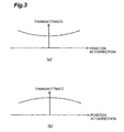
- the first correction filter 8, as shown in Fig. 3 (a), has such a transmission distribution of a quadric concave pattern that the transmittance is minimum at the center of the effective region along the Y-direction and that the transmittance monotonically increases toward the periphery in accordance with a quadratic function of distance from the center, for example.
- the second correction filter 9, as shown in Fig. 3 (b) has such a transmittance distribution of a quadric convex pattern that the transmittance is maximum at the center of the effective region along the Y-direction and that the transmittance monotonically decreases toward the periphery in accordance with a quadratic function of distance from the center, for example.
- the first correction filter 8 a difference between the maximum transmittance in the periphery of the effective region and the minimum transmittance at the center is set, for example, to 4% and in the second correction filter 9 a difference between the minimum transmittance in the periphery of the effective region and the maximum transmittance at the center is set, for example, to 4%.
- the first correction filter 8 has the transmittance distribution of the quadric 4%-concave pattern and the second correction filter 9 the transmittance distribution of the quadric 4%-convex pattern.
- the first correction filter 8 and the second correction filter 9 come to have the transmittance distributions complementary to each other.
- the apparatus is so set that a distance between the first correction filter 8 (precisely, the optical surface thereof on the mask side as an adjustment film) and the mask blind 7 is equal to a distance between the second correction filter 9 (precisely, the optical surface thereof on the light source side as an adjustment film) and the mask blind 7.
- a pupil luminance distribution about the center point P1 a pupil luminance distribution about the point P2, and a pupil luminance distribution about the point P3 all are uniform as indicated by hatched regions above the first correction filter 8 in Fig. 2. That a pupil luminance distribution about a certain point on a surface to be illuminated is uniform is nothing but that a light intensity distribution formed on the illumination pupil plane (e.g., the rear focal plane of the micro fly's eye lens 5) by rays arriving at that point is uniform.
- the pupil luminance distribution about the center point P1 changes from the uniform pattern into a concave pattern
- the pupil luminance distribution about the point P2 changes from the uniform pattern into an inclined pattern
- the pupil luminance distribution about the point P3 changes from the uniform pattern into an inclined pattern inclined in the opposite inclination direction to the inclined pattern of the point P2, as indicated by hatched regions between the first correction filter 8 and the mask blind 7 and between the mask blind 7 and the second correction filter 9 in Fig. 2.
- the adjustment film of the first correction filter 8 outputs light with a light intensity distribution different from that of incident light, and effects the following changes: a change in light intensity distribution from the uniform intensity distribution into a concave intensity distribution when a light beam to arrive at the center point P1 passes through the adjustment film of the first correction filter 8; a change in light intensity distribution from the uniform intensity distribution into an inclined intensity distribution when a light beam to arrive at the point P2 passes through the adjustment film of the first correction filter 8; a change in light intensity distribution from the uniform intensity distribution into an intensity distribution inclined in the opposite direction to the inclined intensity distribution corresponding to the point P2 when a light beam to arrive at the point P3 passes through the adjustment film of the first correction filter 8.
- the second correction filter 9 acts to return the pupil luminance distribution of the concave pattern about the center point P1 to a uniform pattern and to change the inclined patterns of the pupil luminance distributions about the point P2 and the point P3 to inclined patterns with enhanced degree of inclination, as indicated by hatched regions between the second correction filter 9 and the imaging optical system 10 (or imaging optical system 10 + projection optical system PL) and between the imaging optical system 10 (or imaging optical system 10 + projection optical system PL) and the mask M (or the wafer W) in Fig. 2.
- the adjustment film of the second correction filter 9 also outputs light with a light intensity distribution different from that of incident light, and effects the following changes: a change from the light intensity distribution of the concave intensity distribution into a uniform intensity distribution when a light beam to arrive at the center point P1 passes through the adjustment film of the second correction filter 9; a change from the light intensity distribution of the inclined intensity distribution into a further inclined intensity distribution when a light beam to arrive at the point P2 passes through the adjustment film of the second correction filter 9; a change from the light intensity distribution of the inclined intensity distribution into a further inclined intensity distribution when a light beam to arrive at the point P3 passes through the adjustment film of the second correction filter 9.
- the cooperation of the first correction filter 8 and the second correction filter 9 changes the uniform pupil luminance distribution about the point P2 (and points having the same Y-coordinate as P2) to the linear inclination pattern and changes the uniform pupil luminance distribution about the point P3 (and points having the same Y-coordinate as P3) to the linear inclination pattern having the inclination direction opposite to that of the inclination pattern about the point P2 and the same degree of inclination, without change in the uniform pupil luminance distribution about the center point P1 (and points having the same Y-coordinate as P1).
- the degree of adjustment of linear inclination of the pupil luminance distributions about the point P2 and the point P3 is dependent upon the distance of the point P2 and the point P3 along the Y-direction from the center point P1.
- the degree of linear inclination adjustment for a pupil luminance distribution about a certain point increases with distance from the center point P 1 along the Y-direction. It is also apparent with reference to Fig. 2 that a size of a region where rays to arrive at each point on the surface to be illuminated pass through each of the first correction filter 8 and the second correction filter 9 (which will be referred to hereinafter as "partial region") becomes larger as the first correction filter 8 and the second correction filter 9 are set more distant from the mask blind 7, and that the degree of linear inclination adjustment for a pupil luminance distribution about each point also increases therewith.
- the degree of linear inclination adjustment for a pupil luminance distribution about each point also increases as the degree of change in the transmittance distributions of the first correction filter 8 and the second correction filter 9 (4% in the foregoing example) is set larger.
- the present embodiment has the configuration wherein the first correction filter 8 and the second correction filter 9 have the complementary transmittance distributions and wherein the first correction filter 8 and the second correction filter 9 are set equidistant from the mask blind 7 on both sides thereof, as described above, the position and size of the partial region about each point on the surface to be illuminated, in the first correction filter 8 are almost equal to those in the second correction filter 9.
- the pupil luminance distribution about each point on the surface to be illuminated is adjusted on a point-by-point basis by cooperation of the first correction filter 8 and the second correction filter 9, but the illuminance distribution on the surface to be illuminated is maintained almost uniform without substantial change.
- a change state of light intensity distribution imposed by the first correction filter 8 and the second correction filter 9, for the first light beam passing through the first correction filter 8 and the second correction filter 9 is different from a change state of light intensity distribution imposed by the first correction filter 8 and the second correction filter 9, for the second light beam passing through the first correction filter 8 and the second correction filter 9.
- the first correction filter 8 and the second correction filter 9 constitute an adjuster for independently adjusting each of pupil luminance distributions about respective points on the surface to be illuminated (M, W).
- the exposure apparatus of the present embodiment is able to adjust each of pupil luminance distributions at respective points on the surface to be illuminated to being almost uniform, while maintaining the illuminance distribution almost uniform on the surface to be illuminated (M, W); therefore, it is able to accurately transfer the microscopic pattern of the mask M in a desired line width across the entire exposure region onto the wafer W.
- the first correction filter 8 and the second correction filter 9 are set equidistant from the mask blind 7 on both sides thereof; however, the same effect as in the foregoing embodiment is also achieved when they are set equidistant on both sides of a conjugate plane optically conjugate with the wafer W as a final surface to be illuminated, specifically, when they are set equidistant on both sides of the mask M, for example.
- the first correction filter 8 has the transmittance distribution of the quadric concave pattern and the second correction filter 9 has the transmittance distribution of the quadric convex pattern; however, the same effect as in the foregoing embodiment is also achieved in a case where the first correction filter 8 has a transmittance distribution of a quadric convex pattern and where the second correction filter 9 has a transmittance distribution of a quadric concave pattern.
- the first correction filter 8 and the second correction filter 9 have the transmittance distributions of the quadric patterns; however, without having to be limited to this, a variety of modification examples can be contemplated as to the patterns of the transmittance distributions given to the first correction filter 8 and the second correction filter 9.
- the first correction filter 8 has, for example, such a transmittance distribution of a quartic M-shaped pattern that the transmittance increases once and then decreases from the center toward the periphery in accordance with a quartic function of distance from the center of the effective region along the Y-direction, as shown in Fig. 4 (a).
- the second correction filter 9 has such a transmittance distribution of a quartic W-shaped pattern that the transmittance decreases once and then increases from the center toward the periphery in accordance with a quartic function of distance along the Y-direction from the center of the effective region, as shown in Fig. 4 (b).
- the transmittance distribution of the first correction filter 8 is set to be complementary to the transmittance distribution of the second correction filter 9, with the same effect as in the foregoing embodiment.
- the first correction filter 8 and the second correction filter 9 have the transmittance distributions of the quartic patterns, the inclination adjustment effect achieved is not the linear inclination adjustment, but cubical inclination adjustment.
- the first correction filter 8 and the second correction filter 9 may have their respective transmittance distributions whose patterns are higher than the quartic.
- the patterns of the transmittance distributions of the patterns of the first correction filter 8 and the second correction filter 9 may contain an inclination component (linear component).
- they may be transmittance distributions each of which is a combination of an inclination component with a quadratic component (or a quartic or higher component).
- the patterns of the transmittance distributions of the first correction filter 8 and the second correction filter 9 may also be odd-order components such as cubic components.
- the first correction filter 8 and the second correction filter 9 are provided with the respective one-dimensional transmittance distributions along the Y-direction, but it is also possible to contemplate a variety of modification examples as to change directions of the one-dimensional transmittance distributions. It is also possible to provide the first correction filter 8 and the second correction filter 9 with respective two-dimensional transmittance distributions, e.g., rotationally symmetric transmittance distributions.
- the transmittance distributions to be given to the first correction filter 8 and to the second correction filter 9 can also be defined according to other appropriate functions.
- An example is, for example, to define the transmittance distributions of the first correction filter 8 and the second correction filter 9 by later-described Zernike polynomials, whereby each of the pupil luminance distributions about respective points on the surface to be illuminated can be adjusted on a point-by-point basis in accordance with a variety of forms.
- the first correction filter 8 and the second correction filter 9 are provided with the transmittance distributions through the use of the dense patterns of light-blocking dots like chromium dots, it is necessary to evaluate transfer of each dot onto the wafer W and influence of diffraction at each dot and to set the size of each dot, the distances of the first correction filter 8 and the second correction filter 9 from the mask blind 7, and so on.
- the first correction filter 8 and the second correction filter 9 are provided with the transmittance distributions through the use of the dense patterns of light-blocking dots, but, without having to be limited to it, it is also possible to provide the filters with continuously changing transmittance distributions by controlling thicknesses of thin films as the adjustment films.
- the transmittance distributions of optically transparent members themselves forming the first correction filter 8 and the second correction filter 9 may be set to given transmittance distributions.
- the transmittance distributions given to the first correction filter 8 and to the second correction filter 9 are not limited to the continuously changing transmittance distributions, but may be stepwise changing transmittance distributions.
- the transmittance distribution of the first correction filter 8 is set to be complementary to the transmittance distribution of the second correction filter 9; however, without having to be limited to this, it is also possible to contemplate a modification example wherein the second correction filter 9 is provided with a transmittance distribution substantially different from a transmittance distribution complementary to the transmittance distribution of the first correction filter 8.
- the illuminance distribution on the surface to be illuminated is adjusted according to the difference between the transmittance distribution of the second correction filter 9 and the transmittance distribution complementary to the transmittance distribution of the first correction filter 8, whereby it is feasible to adjust each of the pupil luminance distributions at respective points on the surface to be illuminated to being almost uniform, while adjusting the illuminance distribution on the surface to be illuminated to being almost uniform.
- the first correction filter 8 and the second correction filter 9 can also be set at mutually different distances on both sides of the mask blind 7.
- the illuminance distribution on the surface to be illuminated can be adjusted according to the difference between the distance of the first correction filter 8 from the mask blind 7 and the distance of the second correction filter 9 from the mask blind 7, whereby it is eventually feasible to adjust each of the pupil luminance distributions at respective points on the surface to be illuminated to being almost uniform, while adjusting the illuminance distribution on the surface to be illuminated to being almost uniform.
- the first correction filter 8 and the second correction filter 9 have their respective transmittance distributions of transmittances different according to incidence positions, but, without having to be limited to it, it is also possible to contemplate a modification example wherein the pair of correction filters are provided with their respective transmittance distributions of transmittances different according to incidence angles.
- one correction filter 8a is located on the light source side with respect to the pupil plane 10a of the imaging optical system 10 (which is a conjugate plane optically conjugate with the illumination pupil plane), and the other correction filter 9a is located on the mask side with respect to the pupil plane 10a of the imaging optical system 10.
- a first light beam is defined as a light beam to arrive at a first point on the surface to be illuminated and where a second light beam is defined as a light beam to arrive at a second point different from the first point on the surface to be illuminated
- an angle of incidence upon passage of the first light beam through the correction filters 8a and 9a is different from that upon passage of the second light beam through the correction filters 8a and 9a; therefore, a change state of light intensity distribution given to the first light beam by the correction filters 8a and 9a is different from a change state of light intensity distribution given to the second light beam by the correction filters 8a and 9a.
- a correction filter with a transmittance distribution of transmittances different according to incidence positions in combination with a correction filter with a transmittance distribution of transmittances different according to incidence angles, or to use a correction filter pair (8, 9) with respective transmittance distributions of transmittances different according to incidence positions, in combination with a correction filter pair (8a, 9a) with respective transmittance distributions of transmittances different according to incidence angles.
- the pair of correction filters (8, 9; 8a, 9a) are provided with their respective transmittance distributions, but, without having to be limited to this, the same effect is also achieved as in the foregoing embodiment and the foregoing modification examples, by using a first adjustment film and a second adjustment film with their respective reflectance distributions of reflectances different according to incidence positions, or by using a first adjustment film and a second adjustment film with their respective reflectance distributions of reflectances different according to incidence angles. It is also possible to use an adjustment film (correction filter) with a transmittance distribution of transmittances different according to incidence positions or incidence angles, in combination with an adjustment film with a reflectance distribution of reflectances different according to incidence positions or incidence angles.
- the pair of correction filters (8, 9; 8a, 9a) are used, i.e., the pair of adjustment films (adjustment surfaces) in other words are used, to adjust each of pupil luminance distributions at respective points on the surface to be illuminated to being almost uniform, while maintaining or adjusting the illuminance distribution on the surface to be illuminated to being almost uniform.
- the effect of the present invention can also be generally achieved by means of an adjuster comprising a plurality of adjustment films (adjustment surfaces) having predetermined transmittance distributions or reflectance distributions. Namely, it is possible to contemplate a variety of modification examples as to the number and arrangement of the adjustment films (adjustment surfaces) which the adjuster comprises.
- the first correction filter 11 a and the second correction filter 11b are located in order from the light source side in the optical path of the condenser optical system 6 between the micro fly's eye lens 5 and the mask blind 7, and the third correction filter 11c is located in the optical path between the condenser optical system 6 and the mask blind 7.
- the correction filters 11a-11c are located at mutually different positions in the optical-axis direction of the illumination optical apparatus, as shown in Fig. 7, regions where an on-axis light beam (a light beam arriving at an intersection between the mask blind 7 and the optical axis AX) passes through the respective correction filters 11a-11c, i.e., on-axis partial regions 11 aa, 11ba, 11ca are different among the correction filters 11a-11c.
- regions where an off axis light beam (a light beam arriving at a point on the mask blind 7 distant from the optical axis AX) passes through the respective correction filters 11a-11c, i.e., off-axis partial regions 11ab, 11bb, 11cb are also different among the correction filters 11a-11c.
- the effect of the present invention can be generally achieved by properly setting the transmittance distributions (or reflectance distributions) of the respective adjustment surfaces (adjustment films), the positions and sizes of the on-axis partial regions and the off-axis partial regions on the respective adjustment surfaces (adjustment films), and so on, using an adjuster comprising a plurality of adjustment surfaces (adjustment films) having predetermined transmittance distributions (or reflectance distributions) of transmittances (or reflectances) varying according to incidence positions or incidence angles.
- all the correction filters 11a-11c are located in the optical path between the micro fly's eye lens 5 as an optical integrator and the mask blind 7, but these correction filters 11 a-11c may be located in the optical path between the mask blind 7 and the surface to be illuminated, or only one or two of the correction filters (e.g., only the correction filter 11c) may be located in the optical path between the mask blind 7 and the surface to be illuminated.
- the change in the illuminance distribution on the surface to be illuminated may be compensated for, for example, by additionally using a variable slit apparatus as described in International Publication 2005/048326, or an illuminance distribution controlling apparatus as described in U.S. Pat. No. 6,771,350 or the like.
- the adjustment surface (adjustment film) with the predetermined transmittance distribution (or reflectance distribution) is formed on the optical surface of each correction filter having the form of the plane-parallel plate, but, without having to be limited to this, it is also possible to form each adjustment surface (adjustment film) on a surface of a lens or a reflecting mirror, i.e., on a convex lens surface, a concave lens surface, a convex reflecting surface, or a concave reflecting surface. It is, however, a matter of course that it is generally easier to manufacture each adjustment surface (adjustment film) on an optical surface of an optical member having a planar optical surface.
- the configuration from the light source 1 to the projection optical system PL be an illumination optical apparatus for illuminating the wafer W as a surface to be illuminated, and let us describe an adjustment method for adjusting this illumination optical apparatus (1-PL).
- this illumination optical apparatus (1-PL).
- a plurality of (two or more) correction filters having respective predetermined transmittance distributions are used to adjust each of pupil luminance distributions at respective points on the surface to be illuminated to being almost uniform, while adjusting the illuminance distribution on the surface to be illuminated (the surface where the wafer W is set) to being almost uniform.
- Fig. 8 is a flowchart schematically showing steps in an adjustment method of illumination optical apparatus according to the present embodiment.
- the first step is to acquire pupil luminance distributions about a plurality of points on the surface to be illuminated, and an illuminance distribution on the surface to be illuminated (S11).
- the distribution acquisition step S11 is to calculate the pupil luminance distributions about a plurality of points on the surface to be illuminated, and the illuminance distribution on the surface to be illuminated, based on design data of the illumination optical apparatus (1-PL).
- the design data of the illumination optical apparatus (1-PL) used herein includes, for example, data of the optical system (6-PL) from just after the micro fly's eye lens 5 to just before the wafer W, i.e., data such as curvature radii of respective optical surfaces, axial separations of respective optical surfaces, refractive indices and types of optical materials forming the respective optical members, the wavelength of used light, transmittances of the respective optical members, and incidence angle characteristics of antireflection films and reflecting films.
- International Publication WO02/031570 as to how to calculate the pupil luminance distributions about a plurality of points on the surface to be illuminated, based on the design data.
- how to calculate the illuminance distribution on the surface to be illuminated, based on the design data is well known, and reference is made, for example, to Japanese Patent Application Laid-Open No. 3-216658 .
- the distribution acquisition step S11 may be to measure the pupil luminance distributions about a plurality of points on the surface to be illuminated and the illuminance distribution on the surface to be illuminated, for each of apparatus fabricated actually.
- the pupil luminance distributions about a plurality of points on the surface to be illuminated can be measured, for example, with a distribution measuring device 20 shown in Fig. 9.
- the measurement of the pupil luminance distributions with the distribution measuring device 20 is carried out in a state in which the wafer W is retracted from the optical path.
- the distribution measuring device 20 has a pinhole member 20a, a condenser lens 20b, and a photodetector 20c, for example, like a two-dimensional CCD.
- the pinhole member 20a is located at the position of the imaging plane of the projection optical system PL (i.e., a height where an exposed surface of the wafer W is to be positioned during exposure).
- the pinhole member 20a is located at the front focal position of the condenser lens 20b, and the photodetector 20c is located at the rear focal position of the condenser lens 20b. Therefore, a detecting surface of the photodetector 20c is located at a position optically conjugate with the position of aperture stop AS of the projection optical system PL.
- light having passed through the projection optical system PL travels through a pinhole of the pinhole member 20a, is then subject to focusing operation of the condenser lens 20b, and thereafter reaches the detecting surface of the photodetector 20c.
- the distribution measuring device 20 measures the light intensity distribution formed at the position of the aperture stop AS (a position optically conjugate with the rear focal plane of the micro fly's eye lens 5) by a light beam arriving at the pinhole of the pinhole member 20a, i.e., a pupil luminance distribution about the pinhole point on the surface to be illuminated.
- the pupil luminance distributions about a plurality of desired points on the surface to be illuminated can be measured by repeatedly carrying out the measurement while two-dimensionally moving the position of the pinhole of the pinhole member 20a through two-dimensional movement of the wafer stage WS along the plane perpendicular to the optical axis AX of the projection optical system PL.
- the illuminance distribution on the surface to be illuminated can be measured, for example, with an illuminance measuring device 25 shown in Fig. 10.
- the measurement of the illuminance distribution with the illuminance measuring device 25 is also carried out in a state in which the wafer W is retracted from the optical path.
- the illuminance measuring device 25 is provided, for example, with a photodiode 25a as a photodetector for measuring the illuminance distribution on the imaging plane of the projection optical system PL (i.e., the surface to be illuminated).
- the output of photodiode 25a is connected to a signal processor 25b.
- the illuminance measuring device 25 is arranged to successively measure illuminance distribution data at each of positions on the imaging plane of the projection optical system PL via the photodiode 25a through two-dimensional movement of the wafer stage WS along the plane perpendicular to the optical axis AX of the projection optical system PL. It is also possible to adopt a configuration wherein a plurality of photodiodes 25a are two-dimensionally arranged and wherein the illuminance distribution data on the imaging plane of the projection optical system PL is measured all at once, without movement of the wafer stage WS.
- the next step is to determine whether each of the pupil luminance distributions about the plural points on the surface to be illuminated and the illuminance distribution on the surface to be illuminated, which were obtained by the calculation based on the design data or by the measurement using the devices 20 and 25, is almost uniform to a desired extent (S12).
- the flow proceeds to a step S13 of designing correction filters.
- the design step S 13 is to determine (or calculate) the required transmittance distributions to be given to the respective adjustment films, in order to independently adjust each of the pupil luminance distributions about the plural points on the surface to be illuminated and adjust the illuminance distribution on the surface to be illuminated, if necessary, so that both of the pupil luminance distributions and the illuminance distribution can be almost uniform to the desired extent.
- the number and positions of the correction filters to be used are prefigured with reference to the information about the pupil luminance distributions and the illuminance distribution calculated or measured, and the transmittance distributions to be given to the respective correction filters are determined for adjusting each of the pupil luminance distributions at respective points on the surface to be illuminated to being almost uniform, while maintaining or adjusting the illuminance distribution on the surface to be illuminated to being almost uniform.
- the next step is to calculate the pupil luminance distributions about plural points on the surface to be illuminated and the illuminance distribution on the surface to be illuminated, in a state in which the plurality of correction filters with the transmittance distributions determined in the design step S 13 are located at their respective prefigured positions, i.e., in a mounted state of the correction filters (S 14).
- the distribution calculation step S 14 is to calculate the pupil luminance distributions and the illuminance distribution with reference to the information about the transmittance distributions and positions of the respective correction filters in addition to the aforementioned design data information.
- the next step is to determine whether each of the pupil luminance distributions about plural points on the surface to be illuminated and the illuminance distribution on the surface to be illuminated, which were calculated in the distribution calculation step S14, is almost uniform to the desired extent (S12).
- the flow proceeds again to the step S13 of designing correction filters.
- the flow proceeds to the pattern determination step S 15 to determine the dense patterns of light-blocking dots necessary for realizing the required transmittance distributions (transmittance distributions to be given to the respective correction filters) calculated in the design step S13.
- the last step is to manufacture the plurality of correction filters having the dot dense patterns determined in the pattern determination step S 15, and to incorporate the manufactured correction filters at the respective predetermined positions in the optical system (S 16).
- the pattern determination step S15 and the manufacturing-mounting step S16 constitute an adjustment step of forming and placing each of the plurality of adjustment films with the required transmittance distributions. The adjustment method of the present embodiment is completed in this manner.
- Fig. 11 is a flowchart schematically showing steps in the adjustment method according to the modification example of the present embodiment.
- the first step is to acquire the pupil luminance distributions about a plurality of points on the surface to be illuminated and the illuminance distribution on the surface to be illuminated (S21).
- the distribution acquisition step S21 is to calculate the pupil luminance distributions about plural points on the surface to be illuminated and the illuminance distribution on the surface to be illuminated, based on the design data of the illumination optical apparatus (1-PL).
- the aforementioned devices 20 and 25 are used to measure the pupil luminance distributions about plural points on the surface to be illuminated and the illuminance distribution on the surface to be illuminated, for each of apparatus fabricated actually.
- the next step is to determine whether each of the pupil luminance distributions about plural points on the surface to be illuminated and the illuminance distribution on the surface to be illuminated, which were obtained by the calculation based on the design data or by the measurement with the devices 20 and 25, is almost uniform to a desired extent (S22).
- the flow proceeds to an approximation step S23 of the pupil luminance distributions.
- the approximation step S23 of the pupil luminance distributions is to approximate each of the pupil luminance distributions about respective points on the surface to be illuminated, acquired in the distribution acquisition step S21, by a predetermined polynomial as a function of pupil coordinates on the illumination pupil plane.
- a predetermined polynomial as a function of pupil coordinates on the illumination pupil plane.
- the Zernike polynomials including the Zemike cylindrical functions Zi( ⁇ , ⁇ ) using the pupil polar coordinates ( ⁇ , ⁇ ) on the illumination pupil plane as a coordinate system, are used to implement fitting (approximation) of each of the pupil luminance distributions about respective points on the image plane (the surface to be illuminated) of the projection optical system PL.
- the relationship among the image-plane coordinates and pupil coordinates of the projection optical system PL i.e., the relationship among the image-plane orthogonal coordinates (y,z), the pupil orthogonal coordinates ( ⁇ , ⁇ ), the image-plane polar coordinates (h, ⁇ ), and the pupil polar coordinates ( ⁇ , ⁇ ) are as schematically shown in Fig. 12.
- h and ⁇ are normalized radii, and ⁇ and ⁇ radial angles of polar coordinates.
- a pupil luminance distribution I( ⁇ , ⁇ ) is expanded as in Eq (1) below, using the Zernike cylindrical functions Zi( ⁇ , ⁇ ), for each point on the image plane of the projection optical system PL.
- Ci represents coefficients of the respective terms of the Zernike polynomials.
- Table 1 presents the functions Z1-Z36 for the first term to the thirty sixth term, out of the function system Zi( ⁇ , ⁇ ) in the terms of the Zernike polynomials.
- the approximation step S23 is to perform the fitting by the Zernike polynomials for each of the pupil luminance distributions obtained about plural points on the surface to be illuminated (the image plane of the projection optical system PL) and thereby to calculate the Zernike coefficients Ci of the respective terms for each of points.
- the next step is to evaluate the pupil luminance distributions about respective points by a pupil luminance distribution polynomial as a function of the image-plane polar coordinates (h, ⁇ ) and the pupil polar coordinates ( ⁇ , ⁇ ), based on the coefficients Ci of the respective terms in the Zernike polynomials acquired in the approximately step S23 (S24).
- the evaluation step S24 is to set the pupil luminance distribution polynomial that expresses the pupil luminance distributions about respective points as a function of the image-plane polar coordinates (h, ⁇ ) and the pupil polar coordinates ( ⁇ , ⁇ ).
- Concerning the setting of the pupil luminance distribution polynomial reference is made to the specifications and drawings of Japanese Patent Application Laid-Open No. 2003-257812 and Japanese Patent Application No. 2004-149698 .
- the evaluation step S24 is arranged to determine the coefficients of the respective terms in the pupil luminance distribution polynomial, based on the Zemike coefficients Ci of the respective terms in the Zernike polynomials acquired in the approximation step (S23), and thus to express and evaluate the pupil luminance distributions about respective points by the pupil luminance distribution polynomial.
- a Zernike function Zi of a specific term attention is focused, for example, on a Zernike function Zi of a specific term, and a coefficient of the specific term in the pupil luminance distribution polynomial is determined, for example, by the least-square method, based on an in-image-plane distribution of corresponding Zernike coefficients Ci (a distribution of coefficients Ci at respective points).
- the evaluation step S24 results in finally obtaining the pupil luminance distribution polynomial simultaneously expressing the in-pupil distribution and the in-image-plane distribution of pupil luminance distributions.
- the next step S25 of designing correction filters is to determine (or calculate) the required transmittance distributions to be given to the respective adjustment films, in order to independently adjust each of the pupil luminance distributions about plural points on the surface to be illuminated and adjust the illuminance distribution on the surface to be illuminated, if necessary, so that both of the pupil luminance distributions and the illuminance distribution can be almost uniform to the desired extent.
- the initial step which is carried out according to need, is to approximate the illuminance distribution on the surface to be illuminated, which was acquired in the distribution acquisition step S21, by a Zernike polynomial as a function of the image-plane polar coordinates (h, ⁇ ).
- a transmittance distribution to be given to each correction filter is expressed, for example, by a Zernike polynomial of polar coordinates on an optical surface as an adjustment film.
- the following tables are prepared: a first table T21 indicating a relation between the coefficients of the respective terms in the Zernike polynomials expressing the transmittance distributions of the respective correction filters and changes in the pupil luminance distributions about respective points on the surface to be illuminated; and a second table T22 indicating a relation between the coefficients of the respective terms in the Zernike polynomials expressing the transmittance distributions of the respective correction filters and changes in the illuminance distribution on the surface to be illuminated.
- the design step S25 is to determine the transmittance distributions to be given to the respective correction filters, for adjusting each of the pupil luminance distributions at respective points on the surface to be illuminated to being almost uniform, while maintaining or adjusting the illuminance distribution on the surface to be illuminated to being almost uniform, based on an optimization technique by linear coupling with reference to the evaluation result about the pupil luminance distributions acquired in the evaluation step S24 (specifically, the pupil luminance distribution polynomial simultaneously expressing the in-pupil distribution and the in-image-plane distribution of pupil luminance distributions), the illuminance distribution information approximated by the Zernike polynomials if necessary, the correlation between transmittance distributions of the respective correction filters and changes in the pupil luminance distributions in the first table T21, and the correlation between transmittance distributions of the respective correction filters and changes in the illuminance distribution in the second table T22.
- the next step is to calculate the pupil luminance distributions about plural points on the surface to be illuminated and the illuminance distribution on the surface to be illuminated, in a state in which the plurality of correction filters with the transmittance distributions determined in the design step S25 are located at their respective prefigured positions, i.e., in a mounted state of the correction filters (S26). Furthermore, it is determined whether each of the pupil luminance distributions about plural points on the surface to be illuminated and the illuminance distribution on the surface to be illuminated, which were calculated in the distribution calculation step S26, is almost uniform to the desired extent (S22).
- the determination step S22 results in determining that both of the pupil luminance distributions and the illuminance distribution are almost uniform to the desired extent, and the flow proceeds to the step S27 of determining the dot dense patterns of the correction filters.
- the pattern determination step S27 is to determine the dense patterns of light-blocking dots necessary for realizing the required transmittance distributions (the transmittance distributions to be given to the respective correction filters) calculated in the design step S25.
- the last step is to manufacture the plurality of correction filters with the dot dense patterns determined in the pattern determination step S27, and to incorporate the manufactured correction filters at their respective predetermined positions in the optical system (S28).
- the adjustment method of the modification example is completed in this way.
- the application of the technique of actually measuring the pupil luminance distributions and the illuminance distribution, to the distribution acquisition step S11, S21 is extremely useful, for example, in correction for manufacturing errors of apparatus fabricated actually and in correction for temporal changes of apparatus in operation.
- the plurality of adjustment surfaces of the adjuster are not limited to those with the predetermined transmittance distributions or reflectance distributions, but another potential configuration is, for example, such that light with a light intensity distribution different from that of incident light is outputted by changing the density of rays of an incident light beam by use of diffraction of a diffractive optical element.
- the projection optical system can be the catadioptric projection optical system described in International Publication 2004/019128 . It is also possible to use the catadioptric projection optical systems described in International Publication 2004/107011 , International Publication 2005/59617 , and U.S. Published Application No. 2005/0117224 . Among these, the catadioptric projection optical systems described in the foregoing International Publication 2004/019128 and U.S. Published Application No.
- 2005/0117224 include one or more path folding mirrors, and if the path folding mirror causes the pupil luminance distribution on the wafer W as a surface to be illuminated, to have an inclined distribution, one or more of the plurality of adjustment surfaces of the adjuster in each of the forgoing embodiment and modification examples may be provided with a component for compensating for the inclined distribution of the pupil luminance distribution.
- the exposure apparatus of the foregoing embodiment can be used to manufacture microdevices (semiconductor devices, image pickup devices, liquid-crystal display devices, thin-film magnetic heads, etc.) by illuminating a mask (reticle) by the illumination optical apparatus (illumination step) and projecting a pattern to be transferred, formed on the mask, onto a photosensitive substrate with the projection optical system (exposure step).
- a mask reticle
- illumination optical apparatus illumination step
- exposure step projecting a pattern to be transferred, formed on the mask, onto a photosensitive substrate with the projection optical system
- An example of a technique of forming a predetermined circuit pattern on a wafer or the like as a photosensitive substrate with the exposure apparatus of the foregoing embodiment to obtain semiconductor devices as microdevices will be described below with reference to the flowchart of Fig. 13.
- the first step 301 in Fig. 13 is to deposit a metal film on each wafer in one lot.
- the next step 302 is to apply a photoresist onto the metal film on each wafer in the lot.
- the subsequent step 303 is to sequentially transfer an image of a pattern on the mask into each shot area on each wafer in the lot through the projection optical system, using the exposure apparatus of the foregoing embodiment.
- the subsequent step 304 is to perform development of the photoresist on each wafer in the lot and the subsequent step 305 is to perform etching on each wafer in the lot, using the resist pattern as a mask, and thereby to form a circuit pattern corresponding to the pattern on the mask, in each shot area on each wafer.
- Subsequent steps include formation of circuit patterns in upper layers, and others, thereby manufacturing devices such as semiconductor devices.
- the above-described semiconductor device manufacture method permits us to obtain semiconductor devices with extremely fine circuit patterns at high throughput.
- a pattern forming step 401 is to execute a so-called photolithography step to transfer a pattern of a mask onto a photosensitive substrate (glass substrate coated with a resist, or the like) with the exposure apparatus of the foregoing embodiment.
- This photolithography step results in forming the predetermined pattern including a number of electrodes and others on the photosensitive substrate.
- steps such as development, etching, and resist removal, whereby a predetermined pattern is formed on the substrate.
- the process shifts to the next color filter forming step 402.
- the next color filter forming step 402 is to form a color filter in which a number of sets of three dots corresponding to R (Red), G (Green), and B (Blue) are arrayed in a matrix pattern, or in which sets of three stripe filters of R, G, and B are arrayed as a plurality of lines along the horizontal scan line direction.
- a cell assembling step 403 is carried out.
- the cell assembling step 403 is to assemble a liquid crystal panel (liquid crystal cell), using the substrate with the predetermined pattern obtained in the pattern forming step 401, the color filter obtained in the color filter forming step 402, and so on.
- a liquid crystal is poured into between the substrate with the predetermined pattern obtained in the pattern forming step 401 and the color filter obtained in the color filter forming step 402, to manufacture a liquid crystal panel (liquid crystal cell).
- the subsequent module assembling step 404 is to install each of components such as an electric circuit, a backlight, etc. for display operation of the assembled liquid crystal panel (liquid crystal cell) to complete the liquid-crystal display device.
- the above-described method of manufacturing the liquid-crystal display device permits us to obtain the liquid-crystal display device with an extremely fine circuit pattern at high throughput.
- the exposure light was the KrF excimer laser light (wavelength: 248 nm) or the ArF excimer laser light (wavelength: 193 nm), but, without having to be limited to this, the present invention can also be applied to the other appropriate laser light sources, e.g., an F 2 laser light source for supplying laser light of the wavelength of 157 nm.
- the aforementioned embodiment described the present invention with the example of the exposure apparatus provided with the illumination optical apparatus, but it is apparent that the present invention can be applied to the ordinary illumination optical apparatus for illuminating a surface to be illuminated, except for the masks and wafers.
- the technique of filling the optical path between the projection optical system and the photosensitive substrate with a medium having the refractive index of more than 1.1 can be one selected from the method of locally filling the space with the liquid as disclosed in International Publication WO99/49504 , the method of moving a stage holding a substrate as an exposed object, in a liquid bath as disclosed in Japanese Patent Application Laid-Open No. 6-124873 , the method of forming a liquid bath in a predetermined depth on a stage and holding a substrate in the liquid bath as disclosed in Japanese Patent Application Laid-Open No. 10-303114 , and so on.
- the liquid is preferably one that is transparent to the exposure light, that has the refractive index as high as possible, and that is stable against the projection optical system and the photoresist applied on the surface of the substrate; for example, where the KrF excimer laser light or the ArF excimer laser light is used as the exposure light, the liquid can be pure water, deionized water, glycerol (CH 2 [OH]CH[OH]CH 2 [OH]), heptane (C 7 H 16 ), water with H + , Cs - , K + , Cl - , SO 4 2- , or PO 4 2- , water mixed with fine particles of aluminum oxide, isopropanol, hexane, decane, or the like. Where the exposure light is the F 2 laser light, the liquid can be a fluorine-based liquid, for example, such as fluorine oil or perfluoro polyether (PFPE) capable of transmitting the F 2 laser light.
- PFPE perfluoro polyether
Abstract
Description
- The present invention relates to an illumination optical apparatus, an adjustment method of illumination optical apparatus, an exposure apparatus, and an exposure method and, more particularly, to an illumination optical apparatus suitably applicable to exposure apparatus for manufacturing microdevices, such as semiconductor devices, image pickup devices, liquid-crystal display devices, and thin-film magnetic heads, by lithography.
- In the typical exposure apparatus of this type, a light beam emitted from a light source is guided through a fly's eye lens (or microlens array) as an optical integrator to form a secondary light source as a substantive surface illuminant consisting of a lot of light sources. Light beams from the secondary light source are incident to a condenser lens.
- The light beams converged by the condenser lens illuminate a mask with a predetermined pattern thereon in a superposed manner. Light having passed through the pattern of the mask travels through a projection optical system to form an image on a wafer. In this manner the mask pattern is projected (or transferred) onto the wafer as a photosensitive substrate to effect exposure thereof. The pattern formed on the mask is of high integration and a uniform illuminance distribution must be achieved on the wafer in order to accurately transfer this microscopic pattern onto the wafer.
- Furthermore, attention is being focused on the technology of forming the secondary light source of circular shape on the rear focal plane of the fly's eye lens and changing the size thereof to vary the coherency σ of illumination (σ value = diameter of an aperture stop/pupil diameter of a projection optical system, or σ value = exit-side numerical aperture of an illumination optical system/entrance-side numerical aperture of the projection optical system). In addition, attention is also focused on the technology of forming the secondary light source of annular shape or quadrupole shape on the rear focal plane of the fly's eye lens to improve the depth of focus and resolving power of the projection optical system.
- In this case, in order to accurately transfer the microscopic pattern of the mask onto the wafer, it is necessary to adjust a light intensity distribution of the secondary light source formed on the rear focal plane of the fly's eye lens, i.e., a pupil luminance distribution with a predetermined luminance distribution formed on the illumination pupil plane, to a desired shape and to adjust each of pupil luminance distributions about respective points on the wafer as a final surface to be illuminated to being almost uniform. If there is variation in uniformity of the pupil luminance distributions at respective points on the wafer, the line width of the pattern will vary depending upon positions on the wafer and it will result in failing to accurately transfer the microscopic pattern of the mask in a desired line width across an entire exposure region on the wafer.
- An object of the present invention is to provide an illumination optical apparatus capable of adjusting each of pupil luminance distributions at respective points on a surface to be illuminated to being almost uniform, while maintaining or adjusting an illuminance distribution on the surface to be illuminated to being almost uniform. Another object of the present invention is to provide an exposure apparatus and exposure method capable of accurately transferring a microscopic pattern of a mask in a desired line width across an entire exposure region onto a photosensitive substrate, using an illumination optical apparatus capable of maintaining or adjusting an illuminance distribution on a surface to be illuminated to being almost uniform and capable of adjusting pupil luminance distributions at respective points on the surface to be illuminated to being almost uniform.
- In order to achieve the above object, a first aspect of the present invention provides an illumination optical apparatus for illuminating a surface to be illuminated, with a light beam from a light source,
the illumination optical apparatus comprising: - pupil distribution forming means for forming a pupil luminance distribution with a predetermined luminance distribution on an illumination pupil plane; and
- an adjuster for independently adjusting each of pupil luminance distributions about respective points on the surface to be illuminated;
- wherein the adjuster has a plurality of adjustment surfaces each of which is disposed in an optical path between the pupil distribution forming means and the surface to be illuminated, and
- wherein each of the adjustment surfaces outputs light with a light intensity distribution different from a light intensity distribution of incident light.
- A second aspect of the present invention provides an illumination optical apparatus for illuminating a surface to be illuminated, with a light beam from a light source,
the illumination optical apparatus comprising: - pupil distribution forming means for forming a pupil luminance distribution with a predetermined luminance distribution on an illumination pupil plane; and
- an adjuster for independently adjusting each of pupil luminance distributions about respective points on the surface to be illuminated;
- wherein the adjuster has a plurality of adjustment surfaces each of which is disposed in an optical path between the pupil distribution forming means and the surface to be illuminated and has a predetermined transmittance distribution or reflectance distribution, and
- wherein the plurality of adjustment surfaces are located at respective positions different from each other along an optical-axis direction of the illumination optical apparatus.
- A third aspect of the present invention provides an illumination optical apparatus for illuminating a surface to be illuminated, with a light beam from a light source,
the illumination optical apparatus comprising: - a first adjustment surface disposed in an optical path between an illumination pupil plane of the illumination optical apparatus and the surface to be illuminated and in an optical path on the light source side with respect to a conjugate plane optically conjugate with the surface to be illuminated, and having a first transmittance distribution or first reflectance distribution of transmittances or reflectances different according to incidence positions; and
- a second adjustment surface disposed in the optical path between the illumination pupil plane and the surface to be illuminated and in an optical path on the surface-to-be-illuminated side with respect to the conjugate plane optically conjugate with the surface to be illuminated, and having a second transmittance distribution or second reflectance distribution of transmittances or reflectances different according to incidence positions.
- A fourth aspect of the present invention provides an illumination optical apparatus for illuminating a surface to be illuminated, with a light beam from a light source,
the illumination optical apparatus comprising: - a first adjustment surface disposed in an optical path between an illumination pupil plane of the illumination optical apparatus and the surface to be illuminated and in an optical path on the light source side with respect to a conjugate plane optically conjugate with the surface to be illuminated, and having a first transmittance distribution or first reflectance distribution of transmittances or reflectances different according to incidence angles; and
- a second adjustment surface disposed in the optical path between the illumination pupil plane and the surface to be illuminated and in an optical path on the surface-to-be-illuminated side with respect to the conjugate plane optically conjugate with the surface to be illuminated, and having a second transmittance distribution or second reflectance distribution of transmittances or reflectances different according to incidence angles.
- A fifth aspect of the present invention provides an illumination optical apparatus for illuminating a surface to be illuminated, with a light beam from a light source,
the illumination optical apparatus comprising: - a first adjustment surface disposed in an optical path between an illumination pupil plane of the illumination optical apparatus and the surface to be illuminated, and having a first transmittance distribution or first reflectance distribution of transmittances or reflectances different according to incidence positions; and
- a second adjustment surface disposed in the optical path between the illumination pupil plane and the surface to be illuminated, and having a second transmittance distribution or second reflectance distribution of transmittances or reflectances different according to incidence positions;
- wherein a light beam size at a location where a light beam to arrive at a predetermined point on the surface to be illuminated passes through the first adjustment surface is different from a light beam size at a location where the light beam to arrive at the predetermined point on the surface to be illuminated passes through the second adjustment surface.
- A sixth aspect of the present invention provides a method of adjusting the illumination optical apparatus of the first aspect to the fifth aspect,
the adjustment method comprising: - a pupil luminance distribution calculating step of calculating pupil luminance distributions about a plurality of points on the surface to be illuminated, based on design data of the illumination optical apparatus;
- a distribution determining step of determining required transmittance distributions or reflectance distributions to be given to the respective adjustment surfaces, in order to independently adjust each of the pupil luminance distributions about the plurality of points; and
- an adjustment step of forming and placing each of the plurality of adjustment surfaces with the respective required transmittance distributions or reflectance distributions.
- A seventh aspect of the present invention provides a method of adjusting the illumination optical apparatus of the first aspect to the fifth aspect,
the adjustment method comprising: - a pupil luminance distribution measuring step of measuring pupil luminance distributions about a plurality of points on the surface to be illuminated;
- a distribution determining step of determining required transmittance distributions or reflectance distributions to be given to the respective adjustment surfaces, in order to independently adjust each of the pupil luminance distributions about the plurality of points; and
- an adjustment step of forming and placing each of the plurality of adjustment surfaces with the respective required transmittance distributions or reflectance distributions.
- An eighth aspect of the present invention provides a method of adjusting the illumination optical apparatus of the first aspect to the fifth aspect,
the adjustment method comprising: - a pupil luminance distribution acquiring step of acquiring pupil luminance distributions about a plurality of points on the surface to be illuminated;
- an approximation step of approximating each of the pupil luminance distributions about the plurality of points acquired in the pupil luminance distribution acquiring step, by a predetermined polynomial as a function of pupil coordinates on the illumination pupil plane;
- an evaluation step of evaluating the pupil luminance distributions about the plurality of points by a pupil luminance distribution polynomial as a function of image-plane coordinates and the pupil coordinates on the surface to be illuminated, based on coefficients of respective terms in the predetermined polynomial;
- a step of obtaining a correlation between the transmittance distributions or reflectance distributions given to the respective adjustment surfaces and changes of the pupil luminance distributions about the plurality of points;
- a distribution determining step of determining required transmittance distributions or reflectance distributions to be given to the respective adjustment surfaces, in order to independently adjust each of the pupil luminance distributions about the plurality of points, based on a result of the evaluation in the evaluation step and the correlation; and
- an adjustment step of forming and placing each of the plurality of adjustment surfaces with the respective required transmittance distributions or reflectance distributions.
- A ninth aspect of the present invention provides a method of adjusting an illumination optical apparatus for forming a pupil luminance distribution with a predetermined luminance distribution on an illumination pupil plane on the basis of a light beam from a light source and for illuminating a surface to be illuminated, with a light beam from the pupil luminance distribution,
the adjustment method comprising: - a pupil luminance distribution acquiring step of acquiring pupil luminance distributions about a plurality of points on the surface to be illuminated;
- a distribution determining step of determining required transmittance distributions or reflectance distributions at a plurality of positions in an optical path of the illumination optical apparatus, in order to independently adjust each of the pupil luminance distributions about the plurality of points; and
- an adjustment step of forming each of a plurality of adjustment surfaces with the respective required transmittance distributions or reflectance distributions and placing the adjustment surfaces at the plurality of positions.
- A tenth aspect of the present invention provides an exposure apparatus comprising the illumination optical apparatus of the first aspect to the fifth aspect, or an illumination optical apparatus adjusted by the adjustment method of the sixth aspect to the ninth aspect, the exposure apparatus being adapted for projecting a pattern of a mask illuminated by the illumination optical apparatus, onto a photosensitive substrate to effect exposure thereof.
- An eleventh aspect of the present invention provides an exposure method comprising: an illumination step of illuminating a mask with the illumination optical apparatus of the first aspect to the fifth aspect, or with an illumination optical apparatus adjusted by the adjustment method of the sixth aspect to the ninth aspect; and an exposure step of projecting a pattern of the mask onto a photosensitive substrate to effect exposure thereof.
- The illumination optical apparatus of the present invention has the adjuster for independently adjusting each of the pupil luminance distributions about respective points on the surface to be illuminated, e.g., a plurality of adjustment surfaces each of which outputs light with a light intensity distribution different from that of incident light. Therefore, the operation of the plurality of adjustment surfaces which this adjuster comprises enables the apparatus to adjust each of the pupil luminance distributions at respective points on the surface to be illuminated to being almost uniform, while maintaining or adjusting the illuminance distribution on the surface to be illuminated to being almost uniform. The present invention also enables the apparatus to adjust each of the pupil luminance distributions at respective points on the surface to be illuminated, to a desired distribution while maintaining or adjusting the illuminance distribution on the surface to be illuminated, to a desired distribution.
- Since the exposure apparatus and exposure method of the present invention use the illumination optical apparatus capable of maintaining or adjusting the illuminance distribution on the surface to be illuminated to being almost uniform and capable of adjusting the pupil luminance distributions at respective points on the surface to be illuminated to being almost uniform, they are able to accurately transfer a microscopic pattern of a mask in a desired line width across an entire exposure region onto a photosensitive substrate and, in turn, to manufacture good devices with high accuracy. The exposure apparatus and exposure method of the present invention are also able to accurately transfer the microscopic pattern of the mask in a desired line width across an entire exposure region onto the photosensitive substrate, by adjusting each of the pupil luminance distributions at respective points on the surface to be illuminated, to a desired distribution while maintaining or adjusting the illuminance distribution on the surface to be illuminated, to a desired distribution.
-
- Fig. 1 is a drawing schematically showing an overall configuration of an exposure apparatus according to an embodiment of the present invention.
- Fig. 2 is a drawing schematically showing a configuration and operation of a pair of correction filters in the embodiment.
- Fig. 3 is a drawing schematically showing an example of transmittance distributions given to a pair of correction filters.
- Fig. 4 is a drawing schematically showing another example of transmittance distributions given to a pair of correction filters.
- Fig. 5 is a drawing schematically showing a modification example using a pair of correction filters with transmittance distributions of transmittances different according to incidence angles.
- Fig. 6 is a drawing schematically showing a modification example using three correction filters with transmittance distributions of transmittances different according to incidence positions.
- Fig. 7 is a drawing showing cross sections of an on-axis light beam and an off-axis light beam passing through each of the correction filters in the modification example of Fig. 6.
- Fig. 8 is a flowchart schematically showing steps in an adjustment method of illumination optical apparatus according to the embodiment of the present invention.
- Fig. 9 is a drawing schematically showing a configuration of an apparatus for measuring pupil luminance distributions about plural points on a surface to be illuminated.
- Fig. 10 is a drawing schematically showing a configuration of an apparatus for measuring an illuminance distribution on a surface to be illuminated.
- Fig. 11 is a flowchart schematically showing steps in an adjustment method according to a modification example of the embodiment of the present invention.
- Fig. 12 is a drawing to illustrate a relation among image-plane coordinates and pupil coordinates in a projection optical system.
- Fig. 13 is a flowchart of a technique of manufacturing semiconductor devices as microdevices.
- Fig. 14 is a flowchart of a technique of manufacturing a liquid-crystal display device as a microdevice.
- Embodiments of the present invention will be described based on the accompanying drawings. Fig. 1 is a drawing schematically showing an overall configuration of an exposure apparatus according to an embodiment of the present invention. In Fig. 1, the Z-axis is set along a direction of a normal to a wafer W being a photosensitive substrate, the Y-axis along a direction parallel to the paper of Fig. 1 in the surface of the wafer W, and the X-axis along a direction normal to the paper of Fig. 1 in the surface of the wafer W. In Fig. 1, the illumination optical apparatus is arranged to implement normal circular illumination.
- With reference to Fig. 1, the exposure apparatus of the present embodiment is provided with a
light source 1 for supplying exposure light (illumination light). Thelight source 1 used herein can be, for example, a KrF excimer laser light source for supplying light of the wavelength of 248 nm, an ArF excimer laser light source for supplying light of the wavelength of 193 nm, or the like. A nearly parallel light beam emitted along the +Z direction from thelight source 1 has a cross section of a rectangular shape extending oblongly along the X-direction and is incident to abeam expander 2 consisting of a pair oflenses - The
lenses beam expander 2 is expanded in the paper of Fig. 1 and shaped into a light beam having a cross section of a predetermined rectangular shape. The nearly parallel light beam having passed through thebeam expander 2 as a shaping optical system is then deflected into the +Y direction by a path folding mirror and thereafter travels through a diffractive optical element 3 for circular illumination to enter azoom lens 4. An entrance surface of a micro fly'seye lens 5 is positioned near the rear focal plane of thezoom lens 4. - In general, a diffractive optical element is constructed by forming steps at a pitch approximately equal to the wavelength of the exposure light (illumination light) in a substrate, and functions to diffract an incident light beam at desired angles. Specifically, the diffractive optical element 3 converts the parallel light beam of rectangular shape incident along the optical axis AX, into a divergent light beam having a cross section of a circular shape. The diffractive optical element 3 is arranged to be freely inserted into or retracted from the illumination optical path and to be replaceable with another diffractive optical element for annular illumination or diffractive optical element for quadrupole illumination.
- The micro fly's
eye lens 5 is an optical member comprising a lot of microscopic lenses (optical elements) arranged vertically and horizontally and densely. In general, a micro fly's eye lens is constructed, for example, by simultaneously forming a number of microscopic optical surfaces in a plane-parallel glass plate by applying the MEMS technology (lithography + etching, etc.). In this way, the light beam having passed through the diffractive optical element 3 travels through thezoom lens 4 to form, for example, a circular illumination field centered on the optical axis AX, on the entrance surface of the micro fly'seye lens 5 as an optical integrator of the wavefront splitting type. - The size of the circular illumination field formed herein (i.e., the diameter thereof) varies depending upon the focal length of the
zoom lens 4. The light beam incident to the micro fly'seye lens 5 is two-dimensionally split by a lot of microscopic lenses and the split light beams form respective light sources on the rear focal plane of the microscopic lenses which the incident light beam enters. In this manner, a substantive surface illuminant of a circular shape (hereinafter referred to as a "secondary light source") having a light intensity distribution approximately equal to that of the circular illumination field formed by the incident light beam to the micro fly'seye lens 5 is formed on the rear focal plane of the micro fly'seye lens 5. - Light beams from the secondary light source of circular shape formed on the rear focal plane of the micro fly's
eye lens 5 are subject to focusing operation of a condenseroptical system 6 and thereafter illuminate amask blind 7 disposed on a plane optically conjugate with a mask M (and the wafer W eventually), in a superposed manner. This results in forming an illumination field of a rectangular shape similar to the shape of each microscopic lens forming the micro fly'seye lens 5, on themask blind 7. Afirst correction filter 8 is located in front of the mask blind 7 (on the light source side) and asecond correction filter 9 is located behind the mask blind 7 (on the mask side). Configurations and operations of thefirst correction filter 8 and thesecond correction filter 9 will be described later. - The light beams having passed through an aperture (light transmitting portion) of a rectangular shape in the
mask blind 7 are subject to focusing operation of an imagingoptical system 10, are deflected into the -Z direction by a path folding mirror, and thereafter illuminate the mask M with a predetermined pattern formed thereon, in a superposed manner. In this way, the imagingoptical system 10 forms an image of the rectangular aperture of themask blind 7 on the mask M supported on a mask stage MS. Namely, themask blind 7 constitutes a field stop for defining an illumination region formed on the mask M (and the wafer W eventually). - A light beam having passed through the pattern of the mask M travels through a projection optical system PL to form an image of the mask pattern on the wafer W being a photosensitive substrate. Namely, the pattern image is formed in a rectangular region on the wafer W supported on a wafer stage WS so as to correspond to the rectangular illumination field on the mask M. In this way, the pattern of the mask M is sequentially projected into each exposure area of the wafer W by performing one-shot exposure or scan exposure while two-dimensionally driving and controlling the wafer W in a plane (XY plane) perpendicular to the optical axis AX of the projection optical system PL.
- It is noted that annular illumination can be implemented by setting a diffractive optical element for annular illumination instead of the diffractive optical element 3 in the illumination optical path. The diffractive optical element for annular illumination converts the parallel light beam of the rectangular shape incident along the optical axis AX, into a divergent light beam having a cross section of an annular shape. Therefore, the light beam having passed through the diffractive optical element for annular illumination forms, for example, an illumination field of an annular shape centered on the optical axis AX, on the entrance surface of the micro fly's
eye lens 5. As a result, the secondary light source of the annular shape having the light intensity distribution approximately equal to that of the annular illumination field formed on the entrance surface is also formed on the rear focal plane of the micro fly'seye lens 5. - In addition, quadrupole illumination (generally, multi-pole illumination) can be implemented by setting a diffractive optical element for quadrupole illumination (generally, for multi-pole illumination including dipole, octupole, or other illumination) instead of the diffractive optical element 3 in the illumination optical path. The diffractive optical element for quadrupole illumination converts the parallel light beam of the rectangular shape incident along the optical axis AX, into divergent light beams having a cross section of a quadrupole shape. Therefore, the light beams having passed through the diffractive optical element for quadrupole illumination form, for example, an illumination field of a quadrupole shape centered on the optical axis AX, on the entrance surface of the micro fly's
eye lens 5. As a result, the secondary light source of the quadrupole shape having the light intensity distribution approximately equal to that of the quadrupole illumination field formed on the entrance surface is also formed on the rear focal plane of the micro fly'seye lens 5. - Fig. 2 is a drawing schematically showing a configuration and operation of a pair of correction filters in the present embodiment. In the present embodiment, as shown in Fig. 2, the
first correction filter 8 is located in front of the mask blind 7 (on the light source side) and thesecond correction filter 9 behind the mask blind 7 (on the mask side). Namely, thefirst correction filter 8 and thesecond correction filter 9 are positioned at respective positions different from each other along the optical-axis direction of the illumination optical apparatus. Each of thefirst correction filter 8 and thesecond correction filter 9 has a form of a plane-parallel plate and has a transmittance distribution of transmittances different according to incidence positions. Namely, a dense pattern of light-blocking dots of chromium, chromium oxide, or the like is formed as an adjustment film, for example, on each of an optical surface of thefirst correction filter 8 on themask blind 7 side and an optical surface of thesecond correction filter 9 on themask blind 7 side. Namely, the optical surface of thefirst correction filter 8 on themask blind 7 side and the optical surface of thesecond correction filter 9 on themask blind 7 side serve as adjustment surfaces. - Specifically, the
first correction filter 8, as shown in Fig. 3 (a), has such a transmission distribution of a quadric concave pattern that the transmittance is minimum at the center of the effective region along the Y-direction and that the transmittance monotonically increases toward the periphery in accordance with a quadratic function of distance from the center, for example. On the other hand, thesecond correction filter 9, as shown in Fig. 3 (b), has such a transmittance distribution of a quadric convex pattern that the transmittance is maximum at the center of the effective region along the Y-direction and that the transmittance monotonically decreases toward the periphery in accordance with a quadratic function of distance from the center, for example. - In the
first correction filter 8a difference between the maximum transmittance in the periphery of the effective region and the minimum transmittance at the center is set, for example, to 4% and in thesecond correction filter 9 a difference between the minimum transmittance in the periphery of the effective region and the maximum transmittance at the center is set, for example, to 4%. Namely, thefirst correction filter 8 has the transmittance distribution of the quadric 4%-concave pattern and thesecond correction filter 9 the transmittance distribution of the quadric 4%-convex pattern. As a result, thefirst correction filter 8 and thesecond correction filter 9 come to have the transmittance distributions complementary to each other. - In the present embodiment, the apparatus is so set that a distance between the first correction filter 8 (precisely, the optical surface thereof on the mask side as an adjustment film) and the
mask blind 7 is equal to a distance between the second correction filter 9 (precisely, the optical surface thereof on the light source side as an adjustment film) and themask blind 7. Now, let us focus attention on rays arriving at a center point P1 as intersecting with the optical axis AX on the mask M as a surface to be illuminated (or the wafer W as a final surface to be illuminated), rays arriving at a point P2 a predetermined distance apart in the +Y direction from the center point P1, and rays arriving at a point P3 the same distance apart in the -Y direction from the center point P1. - It is assumed herein that in a state in which the
first correction filter 8 and thesecond correction filter 9 are absent, a pupil luminance distribution about the center point P1, a pupil luminance distribution about the point P2, and a pupil luminance distribution about the point P3 all are uniform as indicated by hatched regions above thefirst correction filter 8 in Fig. 2. That a pupil luminance distribution about a certain point on a surface to be illuminated is uniform is nothing but that a light intensity distribution formed on the illumination pupil plane (e.g., the rear focal plane of the micro fly's eye lens 5) by rays arriving at that point is uniform. - When only the
first correction filter 8 with the transmittance distribution of the quadric 4%-concave pattern is present, the pupil luminance distribution about the center point P1 changes from the uniform pattern into a concave pattern, the pupil luminance distribution about the point P2 changes from the uniform pattern into an inclined pattern, and the pupil luminance distribution about the point P3 changes from the uniform pattern into an inclined pattern inclined in the opposite inclination direction to the inclined pattern of the point P2, as indicated by hatched regions between thefirst correction filter 8 and themask blind 7 and between themask blind 7 and thesecond correction filter 9 in Fig. 2. - Namely, the adjustment film of the
first correction filter 8 outputs light with a light intensity distribution different from that of incident light, and effects the following changes: a change in light intensity distribution from the uniform intensity distribution into a concave intensity distribution when a light beam to arrive at the center point P1 passes through the adjustment film of thefirst correction filter 8; a change in light intensity distribution from the uniform intensity distribution into an inclined intensity distribution when a light beam to arrive at the point P2 passes through the adjustment film of thefirst correction filter 8; a change in light intensity distribution from the uniform intensity distribution into an intensity distribution inclined in the opposite direction to the inclined intensity distribution corresponding to the point P2 when a light beam to arrive at the point P3 passes through the adjustment film of thefirst correction filter 8. - Furthermore, when the
second correction filter 9 with the transmittance distribution of the quadric 4%-convex pattern is also present in addition to thefirst correction filter 8, thesecond correction filter 9 acts to return the pupil luminance distribution of the concave pattern about the center point P1 to a uniform pattern and to change the inclined patterns of the pupil luminance distributions about the point P2 and the point P3 to inclined patterns with enhanced degree of inclination, as indicated by hatched regions between thesecond correction filter 9 and the imaging optical system 10 (or imagingoptical system 10 + projection optical system PL) and between the imaging optical system 10 (or imagingoptical system 10 + projection optical system PL) and the mask M (or the wafer W) in Fig. 2. - Namely, the adjustment film of the
second correction filter 9 also outputs light with a light intensity distribution different from that of incident light, and effects the following changes: a change from the light intensity distribution of the concave intensity distribution into a uniform intensity distribution when a light beam to arrive at the center point P1 passes through the adjustment film of thesecond correction filter 9; a change from the light intensity distribution of the inclined intensity distribution into a further inclined intensity distribution when a light beam to arrive at the point P2 passes through the adjustment film of thesecond correction filter 9; a change from the light intensity distribution of the inclined intensity distribution into a further inclined intensity distribution when a light beam to arrive at the point P3 passes through the adjustment film of thesecond correction filter 9. - In other words, the cooperation of the
first correction filter 8 and thesecond correction filter 9 changes the uniform pupil luminance distribution about the point P2 (and points having the same Y-coordinate as P2) to the linear inclination pattern and changes the uniform pupil luminance distribution about the point P3 (and points having the same Y-coordinate as P3) to the linear inclination pattern having the inclination direction opposite to that of the inclination pattern about the point P2 and the same degree of inclination, without change in the uniform pupil luminance distribution about the center point P1 (and points having the same Y-coordinate as P1). The degree of adjustment of linear inclination of the pupil luminance distributions about the point P2 and the point P3 is dependent upon the distance of the point P2 and the point P3 along the Y-direction from the center point P1. - Namely, the degree of linear inclination adjustment for a pupil luminance distribution about a certain point increases with distance from the
center point P 1 along the Y-direction. It is also apparent with reference to Fig. 2 that a size of a region where rays to arrive at each point on the surface to be illuminated pass through each of thefirst correction filter 8 and the second correction filter 9 (which will be referred to hereinafter as "partial region") becomes larger as thefirst correction filter 8 and thesecond correction filter 9 are set more distant from themask blind 7, and that the degree of linear inclination adjustment for a pupil luminance distribution about each point also increases therewith. It is a matter of course that the degree of linear inclination adjustment for a pupil luminance distribution about each point also increases as the degree of change in the transmittance distributions of thefirst correction filter 8 and the second correction filter 9 (4% in the foregoing example) is set larger. - Since the present embodiment has the configuration wherein the
first correction filter 8 and thesecond correction filter 9 have the complementary transmittance distributions and wherein thefirst correction filter 8 and thesecond correction filter 9 are set equidistant from themask blind 7 on both sides thereof, as described above, the position and size of the partial region about each point on the surface to be illuminated, in thefirst correction filter 8 are almost equal to those in thesecond correction filter 9. As a result, the pupil luminance distribution about each point on the surface to be illuminated is adjusted on a point-by-point basis by cooperation of thefirst correction filter 8 and thesecond correction filter 9, but the illuminance distribution on the surface to be illuminated is maintained almost uniform without substantial change. - In the present embodiment, as described above, where a first light beam is defined as a light beam to arrive at a first point (e.g., the point P1) on the surface to be illuminated and where a second light beam is defined as a light beam to arrive at a second point (e.g., the point P2 or P3) different from the first point on the surface to be illuminated, a change state of light intensity distribution imposed by the
first correction filter 8 and thesecond correction filter 9, for the first light beam passing through thefirst correction filter 8 and thesecond correction filter 9 is different from a change state of light intensity distribution imposed by thefirst correction filter 8 and thesecond correction filter 9, for the second light beam passing through thefirst correction filter 8 and thesecond correction filter 9. This makes it feasible to independently adjust each of pupil luminance distributions about respective points (e.g., the first point and the second point) on the surface to be illuminated (M, W). - Namely, in the present embodiment the
first correction filter 8 and thesecond correction filter 9 constitute an adjuster for independently adjusting each of pupil luminance distributions about respective points on the surface to be illuminated (M, W). As a result, the exposure apparatus of the present embodiment is able to adjust each of pupil luminance distributions at respective points on the surface to be illuminated to being almost uniform, while maintaining the illuminance distribution almost uniform on the surface to be illuminated (M, W); therefore, it is able to accurately transfer the microscopic pattern of the mask M in a desired line width across the entire exposure region onto the wafer W. - In the above description, the
first correction filter 8 and thesecond correction filter 9 are set equidistant from themask blind 7 on both sides thereof; however, the same effect as in the foregoing embodiment is also achieved when they are set equidistant on both sides of a conjugate plane optically conjugate with the wafer W as a final surface to be illuminated, specifically, when they are set equidistant on both sides of the mask M, for example. In the above description, thefirst correction filter 8 has the transmittance distribution of the quadric concave pattern and thesecond correction filter 9 has the transmittance distribution of the quadric convex pattern; however, the same effect as in the foregoing embodiment is also achieved in a case where thefirst correction filter 8 has a transmittance distribution of a quadric convex pattern and where thesecond correction filter 9 has a transmittance distribution of a quadric concave pattern. - In the above description, the
first correction filter 8 and thesecond correction filter 9 have the transmittance distributions of the quadric patterns; however, without having to be limited to this, a variety of modification examples can be contemplated as to the patterns of the transmittance distributions given to thefirst correction filter 8 and thesecond correction filter 9. Specifically, for example, it is also possible to contemplate a modification example wherein thefirst correction filter 8 has, for example, such a transmittance distribution of a quartic M-shaped pattern that the transmittance increases once and then decreases from the center toward the periphery in accordance with a quartic function of distance from the center of the effective region along the Y-direction, as shown in Fig. 4 (a). - In this modification example, the
second correction filter 9 has such a transmittance distribution of a quartic W-shaped pattern that the transmittance decreases once and then increases from the center toward the periphery in accordance with a quartic function of distance along the Y-direction from the center of the effective region, as shown in Fig. 4 (b). In this case, the transmittance distribution of thefirst correction filter 8 is set to be complementary to the transmittance distribution of thesecond correction filter 9, with the same effect as in the foregoing embodiment. However, since thefirst correction filter 8 and thesecond correction filter 9 have the transmittance distributions of the quartic patterns, the inclination adjustment effect achieved is not the linear inclination adjustment, but cubical inclination adjustment. It is noted that thefirst correction filter 8 and thesecond correction filter 9 may have their respective transmittance distributions whose patterns are higher than the quartic. The patterns of the transmittance distributions of the patterns of thefirst correction filter 8 and thesecond correction filter 9 may contain an inclination component (linear component). For example, they may be transmittance distributions each of which is a combination of an inclination component with a quadratic component (or a quartic or higher component). The patterns of the transmittance distributions of thefirst correction filter 8 and thesecond correction filter 9 may also be odd-order components such as cubic components. - In the above description, the
first correction filter 8 and thesecond correction filter 9 are provided with the respective one-dimensional transmittance distributions along the Y-direction, but it is also possible to contemplate a variety of modification examples as to change directions of the one-dimensional transmittance distributions. It is also possible to provide thefirst correction filter 8 and thesecond correction filter 9 with respective two-dimensional transmittance distributions, e.g., rotationally symmetric transmittance distributions. The transmittance distributions to be given to thefirst correction filter 8 and to thesecond correction filter 9 can also be defined according to other appropriate functions. An example is, for example, to define the transmittance distributions of thefirst correction filter 8 and thesecond correction filter 9 by later-described Zernike polynomials, whereby each of the pupil luminance distributions about respective points on the surface to be illuminated can be adjusted on a point-by-point basis in accordance with a variety of forms. - Incidentally, in the foregoing embodiment, where the
first correction filter 8 and thesecond correction filter 9 are provided with the transmittance distributions through the use of the dense patterns of light-blocking dots like chromium dots, it is necessary to evaluate transfer of each dot onto the wafer W and influence of diffraction at each dot and to set the size of each dot, the distances of thefirst correction filter 8 and thesecond correction filter 9 from themask blind 7, and so on. In the above description, thefirst correction filter 8 and thesecond correction filter 9 are provided with the transmittance distributions through the use of the dense patterns of light-blocking dots, but, without having to be limited to it, it is also possible to provide the filters with continuously changing transmittance distributions by controlling thicknesses of thin films as the adjustment films. In another configuration, the transmittance distributions of optically transparent members themselves forming thefirst correction filter 8 and thesecond correction filter 9 may be set to given transmittance distributions. The transmittance distributions given to thefirst correction filter 8 and to thesecond correction filter 9 are not limited to the continuously changing transmittance distributions, but may be stepwise changing transmittance distributions. - In the foregoing embodiment, the transmittance distribution of the
first correction filter 8 is set to be complementary to the transmittance distribution of thesecond correction filter 9; however, without having to be limited to this, it is also possible to contemplate a modification example wherein thesecond correction filter 9 is provided with a transmittance distribution substantially different from a transmittance distribution complementary to the transmittance distribution of thefirst correction filter 8. In this modification example, the illuminance distribution on the surface to be illuminated is adjusted according to the difference between the transmittance distribution of thesecond correction filter 9 and the transmittance distribution complementary to the transmittance distribution of thefirst correction filter 8, whereby it is feasible to adjust each of the pupil luminance distributions at respective points on the surface to be illuminated to being almost uniform, while adjusting the illuminance distribution on the surface to be illuminated to being almost uniform. - Similarly, as a modification example of actively adjusting the illuminance distribution on the surface to be illuminated, the
first correction filter 8 and thesecond correction filter 9 can also be set at mutually different distances on both sides of themask blind 7. In this case, the illuminance distribution on the surface to be illuminated can be adjusted according to the difference between the distance of thefirst correction filter 8 from themask blind 7 and the distance of thesecond correction filter 9 from themask blind 7, whereby it is eventually feasible to adjust each of the pupil luminance distributions at respective points on the surface to be illuminated to being almost uniform, while adjusting the illuminance distribution on the surface to be illuminated to being almost uniform. - In the foregoing embodiment, the
first correction filter 8 and thesecond correction filter 9 have their respective transmittance distributions of transmittances different according to incidence positions, but, without having to be limited to it, it is also possible to contemplate a modification example wherein the pair of correction filters are provided with their respective transmittance distributions of transmittances different according to incidence angles. In this modification example, for example as shown in Fig. 5, onecorrection filter 8a is located on the light source side with respect to thepupil plane 10a of the imaging optical system 10 (which is a conjugate plane optically conjugate with the illumination pupil plane), and theother correction filter 9a is located on the mask side with respect to thepupil plane 10a of the imagingoptical system 10. - In this case, where a first light beam is defined as a light beam to arrive at a first point on the surface to be illuminated and where a second light beam is defined as a light beam to arrive at a second point different from the first point on the surface to be illuminated, an angle of incidence upon passage of the first light beam through the
correction filters correction filters correction filters correction filters - In this case, therefore, the same effect is also achieved as in the foregoing embodiment and the foregoing modification examples. Namely, by adopting a configuration wherein the transmittance distributions of the pair of
correction filters correction filters pupil plane 10a of the imagingoptical system 10, it is feasible to adjust each of the pupil luminance distributions at respective points on the surface to be illuminated to being almost uniform, while maintaining the illuminance distribution almost uniform on the surface to be illuminated. - When the transmittance distributions of the pair of
correction filters correction filters pupil plane 10a of the imagingoptical system 10, it is feasible to adjust each of the pupil luminance distributions at respective points on the surface to be illuminated to being almost uniform, while adjusting the illuminance distribution on the surface to be illuminated to being almost uniform. It is also possible to use a correction filter with a transmittance distribution of transmittances different according to incidence positions, in combination with a correction filter with a transmittance distribution of transmittances different according to incidence angles, or to use a correction filter pair (8, 9) with respective transmittance distributions of transmittances different according to incidence positions, in combination with a correction filter pair (8a, 9a) with respective transmittance distributions of transmittances different according to incidence angles. - In the above description, the pair of correction filters (8, 9; 8a, 9a) are provided with their respective transmittance distributions, but, without having to be limited to this, the same effect is also achieved as in the foregoing embodiment and the foregoing modification examples, by using a first adjustment film and a second adjustment film with their respective reflectance distributions of reflectances different according to incidence positions, or by using a first adjustment film and a second adjustment film with their respective reflectance distributions of reflectances different according to incidence angles. It is also possible to use an adjustment film (correction filter) with a transmittance distribution of transmittances different according to incidence positions or incidence angles, in combination with an adjustment film with a reflectance distribution of reflectances different according to incidence positions or incidence angles.
- In the above description, the pair of correction filters (8, 9; 8a, 9a) are used, i.e., the pair of adjustment films (adjustment surfaces) in other words are used, to adjust each of pupil luminance distributions at respective points on the surface to be illuminated to being almost uniform, while maintaining or adjusting the illuminance distribution on the surface to be illuminated to being almost uniform. However, without having to be limited to this, the effect of the present invention can also be generally achieved by means of an adjuster comprising a plurality of adjustment films (adjustment surfaces) having predetermined transmittance distributions or reflectance distributions. Namely, it is possible to contemplate a variety of modification examples as to the number and arrangement of the adjustment films (adjustment surfaces) which the adjuster comprises.
- Specifically, for example as shown in Fig. 6, it is also possible to contemplate a modification example using three correction filters 11 a-11c having their respective transmittance distributions of transmittances different according to incidence positions. In the modification example of Fig. 6, the first correction filter 11 a and the
second correction filter 11b are located in order from the light source side in the optical path of the condenseroptical system 6 between the micro fly'seye lens 5 and themask blind 7, and thethird correction filter 11c is located in the optical path between the condenseroptical system 6 and themask blind 7. - In this case, since the correction filters 11a-11c are located at mutually different positions in the optical-axis direction of the illumination optical apparatus, as shown in Fig. 7, regions where an on-axis light beam (a light beam arriving at an intersection between the
mask blind 7 and the optical axis AX) passes through the respective correction filters 11a-11c, i.e., on-axis partial regions 11 aa, 11ba, 11ca are different among the correction filters 11a-11c. Similarly, regions where an off axis light beam (a light beam arriving at a point on themask blind 7 distant from the optical axis AX) passes through the respective correction filters 11a-11c, i.e., off-axis partial regions 11ab, 11bb, 11cb are also different among the correction filters 11a-11c. - In this modification example, it is feasible to adjust each of pupil luminance distributions at respective points on the surface to be illuminated to being almost uniform, while adjusting the illuminance distribution on the surface to be illuminated to being almost uniform, by properly setting the transmittance distributions of the respective correction filters 11a-11c, the positions and sizes of the on-axis partial regions and the off axis partial regions on the respective correction filters 11a-11c, and so on. Furthermore, the effect of the present invention can be generally achieved by properly setting the transmittance distributions (or reflectance distributions) of the respective adjustment surfaces (adjustment films), the positions and sizes of the on-axis partial regions and the off-axis partial regions on the respective adjustment surfaces (adjustment films), and so on, using an adjuster comprising a plurality of adjustment surfaces (adjustment films) having predetermined transmittance distributions (or reflectance distributions) of transmittances (or reflectances) varying according to incidence positions or incidence angles.
- In this modification example all the correction filters 11a-11c are located in the optical path between the micro fly's
eye lens 5 as an optical integrator and themask blind 7, but these correction filters 11 a-11c may be located in the optical path between themask blind 7 and the surface to be illuminated, or only one or two of the correction filters (e.g., only thecorrection filter 11c) may be located in the optical path between themask blind 7 and the surface to be illuminated. - In each of the foregoing embodiment and modification examples, if there is a change in the illuminance distribution on the surface to be illuminated, the change in the illuminance distribution on the surface to be illuminated may be compensated for, for example, by additionally using a variable slit apparatus as described in International Publication 2005/048326, or an illuminance distribution controlling apparatus as described in
U.S. Pat. No. 6,771,350 or the like. - In the above description, the adjustment surface (adjustment film) with the predetermined transmittance distribution (or reflectance distribution) is formed on the optical surface of each correction filter having the form of the plane-parallel plate, but, without having to be limited to this, it is also possible to form each adjustment surface (adjustment film) on a surface of a lens or a reflecting mirror, i.e., on a convex lens surface, a concave lens surface, a convex reflecting surface, or a concave reflecting surface. It is, however, a matter of course that it is generally easier to manufacture each adjustment surface (adjustment film) on an optical surface of an optical member having a planar optical surface.
- Now, let the configuration from the
light source 1 to the projection optical system PL be an illumination optical apparatus for illuminating the wafer W as a surface to be illuminated, and let us describe an adjustment method for adjusting this illumination optical apparatus (1-PL). In the present embodiment, for simplicity of description of the adjustment method, it is assumed that a plurality of (two or more) correction filters having respective predetermined transmittance distributions are used to adjust each of pupil luminance distributions at respective points on the surface to be illuminated to being almost uniform, while adjusting the illuminance distribution on the surface to be illuminated (the surface where the wafer W is set) to being almost uniform. - Fig. 8 is a flowchart schematically showing steps in an adjustment method of illumination optical apparatus according to the present embodiment. In the adjustment method of illumination optical apparatus (1-PL) according to the present embodiment, as shown in Fig. 8, the first step is to acquire pupil luminance distributions about a plurality of points on the surface to be illuminated, and an illuminance distribution on the surface to be illuminated (S11). Specifically, the distribution acquisition step S11 is to calculate the pupil luminance distributions about a plurality of points on the surface to be illuminated, and the illuminance distribution on the surface to be illuminated, based on design data of the illumination optical apparatus (1-PL).
- The design data of the illumination optical apparatus (1-PL) used herein includes, for example, data of the optical system (6-PL) from just after the micro fly's
eye lens 5 to just before the wafer W, i.e., data such as curvature radii of respective optical surfaces, axial separations of respective optical surfaces, refractive indices and types of optical materials forming the respective optical members, the wavelength of used light, transmittances of the respective optical members, and incidence angle characteristics of antireflection films and reflecting films. Reference is made, for example, to International PublicationWO02/031570 Japanese Patent Application Laid-Open No. 3-216658 - Alternatively, the distribution acquisition step S11 may be to measure the pupil luminance distributions about a plurality of points on the surface to be illuminated and the illuminance distribution on the surface to be illuminated, for each of apparatus fabricated actually. Specifically, the pupil luminance distributions about a plurality of points on the surface to be illuminated can be measured, for example, with a
distribution measuring device 20 shown in Fig. 9. The measurement of the pupil luminance distributions with thedistribution measuring device 20 is carried out in a state in which the wafer W is retracted from the optical path. Thedistribution measuring device 20 has apinhole member 20a, acondenser lens 20b, and aphotodetector 20c, for example, like a two-dimensional CCD. - The
pinhole member 20a is located at the position of the imaging plane of the projection optical system PL (i.e., a height where an exposed surface of the wafer W is to be positioned during exposure). Thepinhole member 20a is located at the front focal position of thecondenser lens 20b, and thephotodetector 20c is located at the rear focal position of thecondenser lens 20b. Therefore, a detecting surface of thephotodetector 20c is located at a position optically conjugate with the position of aperture stop AS of the projection optical system PL. In thedistribution measuring device 20, light having passed through the projection optical system PL travels through a pinhole of thepinhole member 20a, is then subject to focusing operation of thecondenser lens 20b, and thereafter reaches the detecting surface of thephotodetector 20c. - In this way, a light intensity distribution corresponding to that at the position of the aperture stop AS is formed on the detecting surface of the
photodetector 20c. Namely, thedistribution measuring device 20 measures the light intensity distribution formed at the position of the aperture stop AS (a position optically conjugate with the rear focal plane of the micro fly's eye lens 5) by a light beam arriving at the pinhole of thepinhole member 20a, i.e., a pupil luminance distribution about the pinhole point on the surface to be illuminated. Consequently, the pupil luminance distributions about a plurality of desired points on the surface to be illuminated can be measured by repeatedly carrying out the measurement while two-dimensionally moving the position of the pinhole of thepinhole member 20a through two-dimensional movement of the wafer stage WS along the plane perpendicular to the optical axis AX of the projection optical system PL. - The illuminance distribution on the surface to be illuminated can be measured, for example, with an
illuminance measuring device 25 shown in Fig. 10. The measurement of the illuminance distribution with theilluminance measuring device 25 is also carried out in a state in which the wafer W is retracted from the optical path. Theilluminance measuring device 25 is provided, for example, with aphotodiode 25a as a photodetector for measuring the illuminance distribution on the imaging plane of the projection optical system PL (i.e., the surface to be illuminated). The output ofphotodiode 25a is connected to asignal processor 25b. - The
illuminance measuring device 25 is arranged to successively measure illuminance distribution data at each of positions on the imaging plane of the projection optical system PL via thephotodiode 25a through two-dimensional movement of the wafer stage WS along the plane perpendicular to the optical axis AX of the projection optical system PL. It is also possible to adopt a configuration wherein a plurality ofphotodiodes 25a are two-dimensionally arranged and wherein the illuminance distribution data on the imaging plane of the projection optical system PL is measured all at once, without movement of the wafer stage WS. It is also possible to adopt another configuration wherein a plurality ofphotodiodes 25a are linearly arranged and wherein the wafer stage WS is one-dimensionally moved to effect scanning measurement of the illuminance distribution data on the imaging plane of the projection optical system PL. - In the adjustment method of the present embodiment, the next step is to determine whether each of the pupil luminance distributions about the plural points on the surface to be illuminated and the illuminance distribution on the surface to be illuminated, which were obtained by the calculation based on the design data or by the measurement using the
devices - The
design step S 13 is to determine (or calculate) the required transmittance distributions to be given to the respective adjustment films, in order to independently adjust each of the pupil luminance distributions about the plural points on the surface to be illuminated and adjust the illuminance distribution on the surface to be illuminated, if necessary, so that both of the pupil luminance distributions and the illuminance distribution can be almost uniform to the desired extent. Specifically, the number and positions of the correction filters to be used are prefigured with reference to the information about the pupil luminance distributions and the illuminance distribution calculated or measured, and the transmittance distributions to be given to the respective correction filters are determined for adjusting each of the pupil luminance distributions at respective points on the surface to be illuminated to being almost uniform, while maintaining or adjusting the illuminance distribution on the surface to be illuminated to being almost uniform. - The next step is to calculate the pupil luminance distributions about plural points on the surface to be illuminated and the illuminance distribution on the surface to be illuminated, in a state in which the plurality of correction filters with the transmittance distributions determined in the
design step S 13 are located at their respective prefigured positions, i.e., in a mounted state of the correction filters (S 14). Specifically, the distributioncalculation step S 14 is to calculate the pupil luminance distributions and the illuminance distribution with reference to the information about the transmittance distributions and positions of the respective correction filters in addition to the aforementioned design data information. - The next step is to determine whether each of the pupil luminance distributions about plural points on the surface to be illuminated and the illuminance distribution on the surface to be illuminated, which were calculated in the distribution calculation step S14, is almost uniform to the desired extent (S12). When it is determined in the determination step S12 that at least one of the pupil luminance distributions and the illuminance distribution is not so uniform to the desired extent (in the case of NO in the drawing), the flow proceeds again to the step S13 of designing correction filters. On the other hand, when it is determined in the determination step S12 that both of the pupil luminance distributions and the illuminance distribution are almost uniform to the desired extent (in the case of YES in the drawing), the flow proceeds to the step S 15 of determining the dot dense patterns of the correction filters.
- For example, after repetitive trial-and-error execution of the design step S13 and the distribution
calculation step S 14, the flow proceeds to the pattern determination step S 15 to determine the dense patterns of light-blocking dots necessary for realizing the required transmittance distributions (transmittance distributions to be given to the respective correction filters) calculated in the design step S13. The last step is to manufacture the plurality of correction filters having the dot dense patterns determined in the pattern determination step S 15, and to incorporate the manufactured correction filters at the respective predetermined positions in the optical system (S 16). As described above, the pattern determination step S15 and the manufacturing-mounting step S16 constitute an adjustment step of forming and placing each of the plurality of adjustment films with the required transmittance distributions. The adjustment method of the present embodiment is completed in this manner. - The next modification example of the present embodiment will illustrate an adjustment method capable of readily and accurately determining the required transmittance distributions to be given to the respective correction filters, instead of the trial-and-error method. Fig. 11 is a flowchart schematically showing steps in the adjustment method according to the modification example of the present embodiment. In the adjustment method of the modification example shown in Fig. 11, just as in the adjustment method shown in Fig. 8, the first step is to acquire the pupil luminance distributions about a plurality of points on the surface to be illuminated and the illuminance distribution on the surface to be illuminated (S21). Specifically, the distribution acquisition step S21 is to calculate the pupil luminance distributions about plural points on the surface to be illuminated and the illuminance distribution on the surface to be illuminated, based on the design data of the illumination optical apparatus (1-PL). Alternatively, the
aforementioned devices - The next step, just as in the adjustment method shown in Fig. 8, is to determine whether each of the pupil luminance distributions about plural points on the surface to be illuminated and the illuminance distribution on the surface to be illuminated, which were obtained by the calculation based on the design data or by the measurement with the
devices - The approximation step S23 of the pupil luminance distributions is to approximate each of the pupil luminance distributions about respective points on the surface to be illuminated, acquired in the distribution acquisition step S21, by a predetermined polynomial as a function of pupil coordinates on the illumination pupil plane. Specifically, for example, the Zernike polynomials including the Zemike cylindrical functions Zi(ρ,θ) using the pupil polar coordinates (ρ,θ) on the illumination pupil plane as a coordinate system, are used to implement fitting (approximation) of each of the pupil luminance distributions about respective points on the image plane (the surface to be illuminated) of the projection optical system PL. The relationship among the image-plane coordinates and pupil coordinates of the projection optical system PL, i.e., the relationship among the image-plane orthogonal coordinates (y,z), the pupil orthogonal coordinates (ξ,η), the image-plane polar coordinates (h,α), and the pupil polar coordinates (ρ,θ) are as schematically shown in Fig. 12. Among the coordinates, h and ρ are normalized radii, and α and θ radial angles of polar coordinates.
- A pupil luminance distribution I(ρ,θ) is expanded as in Eq (1) below, using the Zernike cylindrical functions Zi(ρ,θ), for each point on the image plane of the projection optical system PL.

- In this equation, Ci represents coefficients of the respective terms of the Zernike polynomials. Table 1 below presents the functions Z1-Z36 for the first term to the thirty sixth term, out of the function system Zi(ρ,θ) in the terms of the Zernike polynomials.
-
TABLE 1 Z1: 1 Z2: ρcosθ Z3: ρsinθ Z4: 2ρ2-1 Z5: ρ2cos2θ Z6 : ρ2sin2θ Z7: (3ρ2-2)ρcosθ Z8: (3ρ2-2)ρsinθ Z9: 6ρ4-6ρ2+1 Z10: ρ3cos3θ Z11: ρ3sin3θ Z12: (4ρ2-3)ρ2cos2θ Z13: (4ρ2-3)ρ2sin2θ Z14: (10ρ4-12ρ2+3)ρcosθ Z15: (10ρ4-12ρ2+3)ρsinθ Z16: 20ρ6-30ρ4+12ρ2-1 Z17: ρ4cos4θ Z18: ρ 4sin4θ Z19: (5ρ2-4)ρ3cos3θ Z20: (5ρ2-4)ρ3sin3θ Z21: (15ρ4-20ρ2+6)ρ2cos2θ Z22: (15ρ4-20ρ2+6)ρ2sin2θ Z23: (35ρ6-60ρ4+30ρ2-4)ρcosθ Z24: (35ρ6-60ρ4+30ρ2-4)ρsinθ Z25: 70ρ8-140ρ6+90ρ4-20ρ2+1 Z26: ρ 5cos5θ Z27: ρ5sin5θ Z28: (6ρ2-5)ρ4cos4θ Z29: (6ρ2-5)ρ4sin4θ Z30: (21ρ4-30ρ2+10)ρ3cos3θ Z31: (21ρ4-30ρ2+10)ρ3sin3θ Z32: (56ρ6-104ρ4+60ρ2-10)ρ2cos2θ Z33: (56ρ6-104ρ4+60ρ2-10)ρ2sin2θ Z34: (126ρ8-280ρ6+210ρ4-60ρ2+5)ρcosθ Z35: (126ρ8-280ρ6+210ρ4-60ρ2+5)ρsinθ Z36: 252ρ10-630ρ8+560ρ6-210ρ4+30ρ2-1 - Therefore, the approximation step S23 is to perform the fitting by the Zernike polynomials for each of the pupil luminance distributions obtained about plural points on the surface to be illuminated (the image plane of the projection optical system PL) and thereby to calculate the Zernike coefficients Ci of the respective terms for each of points. Concerning the fitting technique of the pupil luminance distributions (pupil transmittance distributions) by the Zernike polynomials, reference is made to the aforementioned International Publication
WO02/031570 Japanese Patent Application Laid-Open No. 2004-126010 - In the adjustment method of the present modification example, the next step is to evaluate the pupil luminance distributions about respective points by a pupil luminance distribution polynomial as a function of the image-plane polar coordinates (h,α) and the pupil polar coordinates (ρ,θ), based on the coefficients Ci of the respective terms in the Zernike polynomials acquired in the approximately step S23 (S24). Specifically, the evaluation step S24 is to set the pupil luminance distribution polynomial that expresses the pupil luminance distributions about respective points as a function of the image-plane polar coordinates (h,α) and the pupil polar coordinates (ρ,θ). Concerning the setting of the pupil luminance distribution polynomial, reference is made to the specifications and drawings of Japanese Patent Application Laid-Open No.
2003-257812 Japanese Patent Application No. 2004-149698 - The foregoing Applications describe the setting of an aberration polynomial that expresses the wavefront aberration of the projection optical system as a function of the image-plane polar coordinates (h,α) and the pupil polar coordinates (ρ,θ), and it is apparent that the pupil luminance distribution polynomial can be set by a similar technique. In this manner, the evaluation step S24 is arranged to determine the coefficients of the respective terms in the pupil luminance distribution polynomial, based on the Zemike coefficients Ci of the respective terms in the Zernike polynomials acquired in the approximation step (S23), and thus to express and evaluate the pupil luminance distributions about respective points by the pupil luminance distribution polynomial.
- Specifically, as disclosed in the foregoing Applications and others, attention is focused, for example, on a Zernike function Zi of a specific term, and a coefficient of the specific term in the pupil luminance distribution polynomial is determined, for example, by the least-square method, based on an in-image-plane distribution of corresponding Zernike coefficients Ci (a distribution of coefficients Ci at respective points). Furthermore, attention is focused on a Zernike function Zi of another specific term, and a coefficient of the other term in the pupil luminance distribution polynomial is subsequently determined, for example, by the least-square method, based on an in-image-plane distribution of corresponding Zernike coefficients Ci.
- In this way, the evaluation step S24 results in finally obtaining the pupil luminance distribution polynomial simultaneously expressing the in-pupil distribution and the in-image-plane distribution of pupil luminance distributions. By using the pupil luminance distribution polynomial simultaneously expressing the in-pupil distribution and the in-image-plane distribution of pupil luminance distributions in this way, it becomes feasible to analytically decompose the pupil luminance distributions and to calculate an optical adjustment solution more quickly and accurately than by the trial-and-error technique of numerical optimization with a computer. Namely, it becomes easier to capture features of the pupil luminance distribution situation by the pupil luminance distribution polynomial and it becomes easier to have a perspective on optical adjustment.
- The next step S25 of designing correction filters is to determine (or calculate) the required transmittance distributions to be given to the respective adjustment films, in order to independently adjust each of the pupil luminance distributions about plural points on the surface to be illuminated and adjust the illuminance distribution on the surface to be illuminated, if necessary, so that both of the pupil luminance distributions and the illuminance distribution can be almost uniform to the desired extent. Specifically, the initial step, which is carried out according to need, is to approximate the illuminance distribution on the surface to be illuminated, which was acquired in the distribution acquisition step S21, by a Zernike polynomial as a function of the image-plane polar coordinates (h,α).
- Furthermore, a transmittance distribution to be given to each correction filter is expressed, for example, by a Zernike polynomial of polar coordinates on an optical surface as an adjustment film. The following tables are prepared: a first table T21 indicating a relation between the coefficients of the respective terms in the Zernike polynomials expressing the transmittance distributions of the respective correction filters and changes in the pupil luminance distributions about respective points on the surface to be illuminated; and a second table T22 indicating a relation between the coefficients of the respective terms in the Zernike polynomials expressing the transmittance distributions of the respective correction filters and changes in the illuminance distribution on the surface to be illuminated.
- In this way, the design step S25 is to determine the transmittance distributions to be given to the respective correction filters, for adjusting each of the pupil luminance distributions at respective points on the surface to be illuminated to being almost uniform, while maintaining or adjusting the illuminance distribution on the surface to be illuminated to being almost uniform, based on an optimization technique by linear coupling with reference to the evaluation result about the pupil luminance distributions acquired in the evaluation step S24 (specifically, the pupil luminance distribution polynomial simultaneously expressing the in-pupil distribution and the in-image-plane distribution of pupil luminance distributions), the illuminance distribution information approximated by the Zernike polynomials if necessary, the correlation between transmittance distributions of the respective correction filters and changes in the pupil luminance distributions in the first table T21, and the correlation between transmittance distributions of the respective correction filters and changes in the illuminance distribution in the second table T22.
- The next step is to calculate the pupil luminance distributions about plural points on the surface to be illuminated and the illuminance distribution on the surface to be illuminated, in a state in which the plurality of correction filters with the transmittance distributions determined in the design step S25 are located at their respective prefigured positions, i.e., in a mounted state of the correction filters (S26). Furthermore, it is determined whether each of the pupil luminance distributions about plural points on the surface to be illuminated and the illuminance distribution on the surface to be illuminated, which were calculated in the distribution calculation step S26, is almost uniform to the desired extent (S22). Since the required transmittance distributions were readily and accurately determined by the optimization technique based on linear coupling, instead of the trial-and-error method, the determination step S22 results in determining that both of the pupil luminance distributions and the illuminance distribution are almost uniform to the desired extent, and the flow proceeds to the step S27 of determining the dot dense patterns of the correction filters.
- The pattern determination step S27 is to determine the dense patterns of light-blocking dots necessary for realizing the required transmittance distributions (the transmittance distributions to be given to the respective correction filters) calculated in the design step S25. The last step is to manufacture the plurality of correction filters with the dot dense patterns determined in the pattern determination step S27, and to incorporate the manufactured correction filters at their respective predetermined positions in the optical system (S28). The adjustment method of the modification example is completed in this way.
- In the above-described embodiment and modification example of the adjustment method, the application of the technique of actually measuring the pupil luminance distributions and the illuminance distribution, to the distribution acquisition step S11, S21 is extremely useful, for example, in correction for manufacturing errors of apparatus fabricated actually and in correction for temporal changes of apparatus in operation.
- In each of the embodiment and modification examples as described above, the plurality of adjustment surfaces of the adjuster are not limited to those with the predetermined transmittance distributions or reflectance distributions, but another potential configuration is, for example, such that light with a light intensity distribution different from that of incident light is outputted by changing the density of rays of an incident light beam by use of diffraction of a diffractive optical element.
- In each of the above-described embodiment and modification examples, the projection optical system can be the catadioptric projection optical system described in International Publication
2004/019128 . It is also possible to use the catadioptric projection optical systems described in International Publication2004/107011 , International Publication2005/59617 U.S. Published Application No. 2005/0117224 . Among these, the catadioptric projection optical systems described in the foregoing International Publication2004/019128 andU.S. Published Application No. 2005/0117224 include one or more path folding mirrors, and if the path folding mirror causes the pupil luminance distribution on the wafer W as a surface to be illuminated, to have an inclined distribution, one or more of the plurality of adjustment surfaces of the adjuster in each of the forgoing embodiment and modification examples may be provided with a component for compensating for the inclined distribution of the pupil luminance distribution. - The exposure apparatus of the foregoing embodiment can be used to manufacture microdevices (semiconductor devices, image pickup devices, liquid-crystal display devices, thin-film magnetic heads, etc.) by illuminating a mask (reticle) by the illumination optical apparatus (illumination step) and projecting a pattern to be transferred, formed on the mask, onto a photosensitive substrate with the projection optical system (exposure step). An example of a technique of forming a predetermined circuit pattern on a wafer or the like as a photosensitive substrate with the exposure apparatus of the foregoing embodiment to obtain semiconductor devices as microdevices will be described below with reference to the flowchart of Fig. 13.
- The
first step 301 in Fig. 13 is to deposit a metal film on each wafer in one lot. Thenext step 302 is to apply a photoresist onto the metal film on each wafer in the lot. Thesubsequent step 303 is to sequentially transfer an image of a pattern on the mask into each shot area on each wafer in the lot through the projection optical system, using the exposure apparatus of the foregoing embodiment. Thesubsequent step 304 is to perform development of the photoresist on each wafer in the lot and thesubsequent step 305 is to perform etching on each wafer in the lot, using the resist pattern as a mask, and thereby to form a circuit pattern corresponding to the pattern on the mask, in each shot area on each wafer. Subsequent steps include formation of circuit patterns in upper layers, and others, thereby manufacturing devices such as semiconductor devices. The above-described semiconductor device manufacture method permits us to obtain semiconductor devices with extremely fine circuit patterns at high throughput. - The exposure apparatus of the foregoing embodiment can also be used to manufacture a liquid-crystal display device as a microdevice by forming predetermined patterns (circuit pattern, electrode pattern, etc.) on plates (glass substrates). An example of a technique in this case will be described with reference to the flowchart of Fig. 14. In Fig. 14, a
pattern forming step 401 is to execute a so-called photolithography step to transfer a pattern of a mask onto a photosensitive substrate (glass substrate coated with a resist, or the like) with the exposure apparatus of the foregoing embodiment. This photolithography step results in forming the predetermined pattern including a number of electrodes and others on the photosensitive substrate. Thereafter, the exposed substrate is subjected to each of steps such as development, etching, and resist removal, whereby a predetermined pattern is formed on the substrate. Thereafter, the process shifts to the next colorfilter forming step 402. - The next color
filter forming step 402 is to form a color filter in which a number of sets of three dots corresponding to R (Red), G (Green), and B (Blue) are arrayed in a matrix pattern, or in which sets of three stripe filters of R, G, and B are arrayed as a plurality of lines along the horizontal scan line direction. After completion of the colorfilter forming step 402, acell assembling step 403 is carried out. Thecell assembling step 403 is to assemble a liquid crystal panel (liquid crystal cell), using the substrate with the predetermined pattern obtained in thepattern forming step 401, the color filter obtained in the colorfilter forming step 402, and so on. - In the
cell assembling step 403, for example, a liquid crystal is poured into between the substrate with the predetermined pattern obtained in thepattern forming step 401 and the color filter obtained in the colorfilter forming step 402, to manufacture a liquid crystal panel (liquid crystal cell). The subsequentmodule assembling step 404 is to install each of components such as an electric circuit, a backlight, etc. for display operation of the assembled liquid crystal panel (liquid crystal cell) to complete the liquid-crystal display device. The above-described method of manufacturing the liquid-crystal display device permits us to obtain the liquid-crystal display device with an extremely fine circuit pattern at high throughput. - In the foregoing embodiment the exposure light was the KrF excimer laser light (wavelength: 248 nm) or the ArF excimer laser light (wavelength: 193 nm), but, without having to be limited to this, the present invention can also be applied to the other appropriate laser light sources, e.g., an F2 laser light source for supplying laser light of the wavelength of 157 nm. Furthermore, the aforementioned embodiment described the present invention with the example of the exposure apparatus provided with the illumination optical apparatus, but it is apparent that the present invention can be applied to the ordinary illumination optical apparatus for illuminating a surface to be illuminated, except for the masks and wafers.
- In the foregoing embodiment, it is also possible to adopt a technique of filling the optical path between the projection optical system and the photosensitive substrate with a medium having the refractive index of more than 1.1 (typically, a liquid), i.e., the so-called liquid immersion method. In this case, the technique of filling the optical path between the projection optical system and the photosensitive substrate with the liquid can be one selected from the method of locally filling the space with the liquid as disclosed in
International Publication WO99/49504 Japanese Patent Application Laid-Open No. 6-124873 Japanese Patent Application Laid-Open No. 10-303114 - The liquid is preferably one that is transparent to the exposure light, that has the refractive index as high as possible, and that is stable against the projection optical system and the photoresist applied on the surface of the substrate; for example, where the KrF excimer laser light or the ArF excimer laser light is used as the exposure light, the liquid can be pure water, deionized water, glycerol (CH2[OH]CH[OH]CH2[OH]), heptane (C7H16), water with H+, Cs-, K+, Cl-, SO4 2-, or PO4 2-, water mixed with fine particles of aluminum oxide, isopropanol, hexane, decane, or the like. Where the exposure light is the F2 laser light, the liquid can be a fluorine-based liquid, for example, such as fluorine oil or perfluoro polyether (PFPE) capable of transmitting the F2 laser light.
-
- 1 light source
- 3 diffractive optical element
- 4 zoom lens
- 5 micro fly's eye lens (fly's eye lens)
- 6 condenser optical system
- 7 mask blind
- 8, 8a, 9, 9a correction filters
- 10 imaging optical system
- 20 distribution measuring device
- 25 illuminance measuring device
- M mask
- MS mask stage
- PL projection optical system
- W wafer
- WS wafer stage
Claims (51)
- An illumination optical apparatus for illuminating a surface to be illuminated, with a light beam from a light source,
the illumination optical apparatus comprising:pupil distribution forming means for forming a pupil luminance distribution with a predetermined luminance distribution on an illumination pupil plane; andan adjuster for independently adjusting each of pupil luminance distributions about respective points on the surface to be illuminated;wherein the adjuster has a plurality of adjustment surfaces each of which is disposed in an optical path between the pupil distribution forming means and the surface to be illuminated, andwherein each of the adjustment surfaces outputs light with a light intensity distribution different from a light intensity distribution of incident light. - An illumination optical apparatus according to claim 1, wherein, where a first light beam is defined as a light beam arriving at a first point on the surface to be illuminated and where a second light beam is defined as a light beam arriving at a second point different from the first point on the surface to be illuminated, a change of light intensity distribution imposed by passage of the first light beam through the plurality of adjustment surfaces is different from a change of light intensity distribution imposed by passage of the second light beam through the plurality of adjustment surfaces.
- An illumination optical apparatus according to claim 1 or 2, wherein the plurality of adjustment surfaces are located at respective positions different from each other along an optical-axis direction of the illumination optical apparatus.
- An illumination optical apparatus according to any one of claims 1 to 3, wherein each of the adjustment surfaces has a predetermined transmittance distribution or reflectance distribution.
- An illumination optical apparatus for illuminating a surface to be illuminated, with a light beam from a light source,
the illumination optical apparatus comprising:pupil distribution forming means for forming a pupil luminance distribution with a predetermined luminance distribution on an illumination pupil plane; andan adjuster for independently adjusting each of pupil luminance distributions about respective points on the surface to be illuminated;wherein the adjuster has a plurality of adjustment surfaces each of which is disposed in an optical path between the pupil distribution forming means and the surface to be illuminated and has a predetermined transmittance distribution or reflectance distribution, andwherein the plurality of adjustment surfaces are located at respective positions different from each other along an optical-axis direction of the illumination optical apparatus. - An illumination optical apparatus according to claim 4 or 5, wherein the adjuster comprises a first adjustment surface having a first transmittance distribution or first reflectance distribution of transmittances or reflectances different according to incidence positions; and a second adjustment surface having a second transmittance distribution or second reflectance distribution substantially complementary to the first transmittance distribution or the first reflectance distribution.
- An illumination optical apparatus according to claim 6, wherein the first adjustment surface is located on the light source side with respect to a conjugate plane optically conjugate with the surface to be illuminated, and wherein the second adjustment surface is located on the surface-to-be-illuminated side with respect to the conjugate plane.
- An illumination optical apparatus according to claim 7, wherein a distance between the first adjustment surface and the conjugate plane is substantially equal to a distance between the second adjustment surface and the conjugate plane.
- An illumination optical apparatus according to claim 7, wherein a first distance between the first adjustment surface and the conjugate plane is substantially different from a second distance between the second adjustment surface and the conjugate plane.
- An illumination optical apparatus according to claim 4 or 5, wherein the adjuster comprises a first adjustment surface having a first transmittance distribution or first reflectance distribution of transmittances or reflectances different according to incidence positions; and a second adjustment surface having a second transmittance distribution or second reflectance distribution substantially different from a transmittance distribution or reflectance distribution complementary to the first transmittance distribution or the first reflectance distribution.
- An illumination optical apparatus according to claim 10, wherein the first adjustment surface is located on the light source side with respect to a conjugate plane optically conjugate with the surface to be illuminated, and wherein the second adjustment surface is located on the surface-to-be-illuminated side with respect to the conjugate plane.
- An illumination optical apparatus according to claim 10 or 11, wherein the adjuster adjusts an illuminance distribution on the surface to be illuminated, according to a difference between the complementary transmittance distribution or reflectance distribution and the second transmittance distribution or the second reflectance distribution.
- An illumination optical apparatus according to claim 4 or 5, wherein the adjuster comprises a first adjustment surface having a first transmittance distribution or first reflectance distribution of transmittances or reflectances different according to incidence angles; and a second adjustment surface having a second transmittance distribution or second reflectance distribution substantially complementary to the first transmittance distribution or the first reflectance distribution.
- An illumination optical apparatus according to claim 13, wherein the first adjustment surface is located on the light source side with respect to a conjugate plane optically conjugate with the illumination pupil plane, and wherein the second adjustment surface is located on the surface-to-be-illuminated side with respect to the conjugate plane.
- An illumination optical apparatus according to claim 14,
wherein a distance between the first adjustment surface and the conjugate plane is substantially equal to a distance between the second adjustment surface and the conjugate plane. - An illumination optical apparatus according to claim 14, wherein a first distance between the first adjustment surface and the conjugate plane is substantially different from a second distance between the second adjustment surface and the conjugate plane.
- An illumination optical apparatus according to claim 4 or 5, wherein the adjuster comprises a first adjustment surface having a first transmittance distribution or first reflectance distribution of transmittances or reflectances different according to incidence angles; and a second adjustment surface having a second transmittance distribution or second reflectance distribution substantially different from a transmittance distribution or reflectance distribution complementary to the first transmittance distribution or the first reflectance distribution.
- An illumination optical apparatus according to claim 17, wherein the first adjustment surface is located on the light source side with respect to a conjugate plane optically conjugate with the illumination pupil plane, and wherein the second adjustment surface is located on the surface-to-be-illuminated side with respect to the conjugate plane.
- An illumination optical apparatus according to claim 17 or 18, wherein the adjuster adjusts an illuminance distribution on the surface to be illuminated, according to a difference between the complementary transmittance distribution or reflectance distribution and the second transmittance distribution or the second reflectance distribution.
- An illumination optical apparatus according to any one of claims 4 to 19, wherein the transmittance distribution or reflectance distribution of each of the adjustment surfaces is an even-order distribution.
- An illumination optical apparatus according to any one of claims 1 to 7, 9 to 14, and 16 to 19, wherein the plurality of adjustment surfaces include a first adjustment surface and a second adjustment surface, and
wherein a light beam size at a location where a light beam to arrive at a predetermined point on the surface to be illuminated passes through the first adjustment surface is different from a light beam size at a location where the light beam to arrive at the predetermined point on the surface to be illuminated passes through the second adjustment surface. - An illumination optical apparatus according to claim 4 or 5, wherein the adjuster comprises a first adjustment surface having a first transmittance distribution or first reflectance distribution of transmittances or reflectances different according to incidence positions; and a second adjustment surface having a second transmittance distribution or second reflectance distribution of transmittances or reflectances different according to incidence angles.
- An illumination optical apparatus according to any one of claims 1 to 22, wherein each of the adjustment surfaces is formed on a plane of an optical member having said plane.
- An illumination optical apparatus for illuminating a surface to be illuminated, with a light beam from a light source, the illumination optical apparatus comprising:a first adjustment surface disposed in an optical path between an illumination pupil plane of the illumination optical apparatus and the surface to be illuminated and in an optical path on the light source side with respect to a conjugate plane optically conjugate with the surface to be illuminated, and having a first transmittance distribution or first reflectance distribution of transmittances or reflectances different according to incidence positions; anda second adjustment surface disposed in the optical path between the illumination pupil plane and the surface to be illuminated and in an optical path on the surface-to-be-illuminated side with respect to the conjugate plane optically conjugate with the surface to be illuminated, and having a second transmittance distribution or second reflectance distribution of transmittances or reflectances different according to incidence positions.
- An illumination optical apparatus according to claim 24, wherein the second transmittance distribution or the second reflectance distribution is substantially complementary to the first transmittance distribution or the first reflectance distribution.
- An illumination optical apparatus according to claim 24, wherein the second transmittance distribution or the second reflectance distribution is substantially different from a transmittance distribution or reflectance distribution substantially complementary to the first transmittance distribution or the first reflectance distribution.
- An illumination optical apparatus for illuminating a surface to be illuminated, with a light beam from a light source, the illumination optical apparatus comprising:a first adjustment surface disposed in an optical path between an illumination pupil plane of the illumination optical apparatus and the surface to be illuminated and in an optical path on the light source side with respect to a conjugate plane optically conjugate with the surface to be illuminated, and having a first transmittance distribution or first reflectance distribution of transmittances or reflectances different according to incidence angles; anda second adjustment surface disposed in the optical path between the illumination pupil plane and the surface to be illuminated and in an optical path on the surface-to-be-illuminated side with respect to the conjugate plane optically conjugate with the surface to be illuminated, and having a second transmittance distribution or second reflectance distribution of transmittances or reflectances different according to incidence angles.
- An illumination optical apparatus according to claim 27, wherein the second transmittance distribution or the second reflectance distribution is substantially complementary to the first transmittance distribution or the first reflectance distribution.
- An illumination optical apparatus according to claim 27, wherein the second transmittance distribution or the second reflectance distribution is substantially different from a transmittance distribution or reflectance distribution substantially complementary to the first transmittance distribution or the first reflectance distribution.
- An illumination optical apparatus for illuminating a surface to be illuminated, with a light beam from a light source, the illumination optical apparatus comprising:a first adjustment surface disposed in an optical path between an illumination pupil plane of the illumination optical apparatus and the surface to be illuminated, and having a first transmittance distribution or first reflectance distribution of transmittances or reflectances different according to incidence positions; anda second adjustment surface disposed in the optical path between the illumination pupil plane and the surface to be illuminated, and having a second transmittance distribution or second reflectance distribution of transmittances or reflectances different according to incidence positions;wherein a light beam size at a location where a light beam to arrive at a predetermined point on the surface to be illuminated passes through the first adjustment surface is different from a light beam size at a location where the light beam to arrive at the predetermined point on the surface to be illuminated passes through the second adjustment surface.
- A method of adjusting the illumination optical apparatus according to any one of claims 1 to 30,
the adjustment method comprising:a pupil luminance distribution calculating step of calculating pupil luminance distributions about a plurality of points on the surface to be illuminated, based on design data of the illumination optical apparatus;a distribution determining step of determining required transmittance distributions or reflectance distributions to be given to the respective adjustment surfaces, in order to independently adjust each of the pupil luminance distributions about the plurality of points; andan adjustment step of forming and placing each of the plurality of adjustment surfaces with the respective required transmittance distributions or reflectance distributions. - An adjustment method according to claim 31, further comprising an illuminance distribution calculating step of calculating an illuminance distribution on the surface to be illuminated, based on the design data,
wherein the distribution determining step comprises calculating the required transmittance distributions or reflectance distributions to be given to the respective adjustment surfaces, in order to adjust the illuminance distribution. - A method of adjusting the illumination optical apparatus according to any one of claims 1 to 30,
the adjustment method comprising:a pupil luminance distribution measuring step of measuring pupil luminance distributions about a plurality of points on the surface to be illuminated;a distribution determining step of determining required transmittance distributions or reflectance distributions to be given to the respective adjustment surfaces, in order to independently adjust each of the pupil luminance distributions about the plurality of points; andan adjustment step of forming and placing each of the plurality of adjustment surfaces with the respective required transmittance distributions or reflectance distributions. - An adjustment method according to claim 33, further comprising an illuminance distribution measuring step of measuring an illuminance distribution on the surface to be illuminated,
wherein the distribution determining step comprises calculating the required transmittance distributions or reflectance distributions to be given to the respective adjustment surfaces, in order to adjust the illuminance distribution. - A method of adjusting the illumination optical apparatus according to any one of claims 1 to 30,
the adjustment method comprising:a pupil luminance distribution acquiring step of acquiring pupil luminance distributions about a plurality of points on the surface to be illuminated;an approximation step of approximating each of the pupil luminance distributions about the plurality of points acquired in the pupil luminance distribution acquiring step, by a predetermined polynomial as a function of pupil coordinates on the illumination pupil plane;an evaluation step of evaluating the pupil luminance distributions about the plurality of points by a pupil luminance distribution polynomial as a function of image-plane coordinates and the pupil coordinates on the surface to be illuminated, based on coefficients of respective terms in said predetermined polynomial;a step of obtaining a correlation between the transmittance distributions or reflectance distributions given to the respective adjustment surfaces and changes of the pupil luminance distributions about the plurality of points;a distribution determining step of determining required transmittance distributions or reflectance distributions to be given to the respective adjustment surfaces, in order to independently adjust each of the pupil luminance distributions about the plurality of points, based on a result of the evaluation in the evaluation step and the correlation; andan adjustment step of forming and placing each of the plurality of adjustment surfaces with the respective required transmittance distributions or reflectance distributions. - An adjustment method according to claim 35, further comprising an illuminance distribution acquiring step of acquiring an illuminance distribution on the surface to be illuminated; and a step of obtaining a second correlation between the transmittance distributions or reflectance distributions given to the respective adjustment surfaces and changes of the illuminance distribution on the surface to be illuminated,
wherein the distribution determining step comprises determining the required transmittance distributions or reflectance distributions to be given to the respective adjustment surfaces, in order to adjust the illuminance distribution, based on the second correlation. - An adjustment method according to claim 35 or 36,
wherein the pupil luminance distribution acquiring step comprises calculating the pupil luminance distributions about the plurality of points on the surface to be illuminated, based on design data of the illumination optical apparatus. - An adjustment method according to claim 35 or 36, wherein the pupil luminance distribution acquiring step comprises measuring the pupil luminance distributions about the plurality of points on the surface to be illuminated.
- An adjustment method according to any one of claims 36 to 38, wherein the illuminance distribution acquiring step comprises calculating the illuminance distribution on the surface to be illuminated, based on the design data of the illumination optical apparatus.
- An adjustment method according to any one of claims 36 to 38, wherein the illuminance distribution acquiring step comprises measuring the illuminance distribution on the surface to be illuminated.
- A method of adjusting an illumination optical apparatus for forming a pupil luminance distribution with a predetermined luminance distribution on an illumination pupil plane on the basis of a light beam from a light source and for illuminating a surface to be illuminated, with a light beam from the pupil luminance distribution,
the adjustment method comprising:a pupil luminance distribution acquiring step of acquiring pupil luminance distributions about a plurality of points on the surface to be illuminated;a distribution determining step of determining required transmittance distributions or reflectance distributions at a plurality of positions in an optical path of the illumination optical apparatus, in order to independently adjust each of the pupil luminance distributions about the plurality of points; andan adjustment step of forming each of a plurality of adjustment surfaces with the respective required transmittance distributions or reflectance distributions and placing the adjustment surfaces at the plurality of positions. - An adjustment method according to claim 41, further comprising an illuminance distribution acquiring step of acquiring an illuminance distribution on the surface to be illuminated,
wherein the distribution determining step comprises calculating the required transmittance distributions or reflectance distributions at the plurality of positions in the optical path of the illumination optical apparatus, in order to adjust the illuminance distribution. - An adjustment method according to claim 42, wherein the illuminance distribution acquiring step comprises calculating the illuminance distribution on the surface to be illuminated, based on design data of the illumination optical apparatus.
- An adjustment method according to claim 42, wherein the illuminance distribution acquiring step comprises measuring the illuminance distribution on the surface to be illuminated.
- An adjustment method according to any one of claims 41 to 44, wherein the pupil distribution acquiring step comprises calculating the pupil luminance distributions about the plurality of points on the surface to be illuminated, based on design data of the illumination optical apparatus.
- An adjustment method according to any one of claims 41 to 44, wherein the pupil distribution acquiring step comprises measuring the pupil luminance distributions about the plurality of points on the surface to be illuminated.
- An exposure apparatus comprising the illumination optical apparatus according to any one of claims 1 to 30, or an illumination optical apparatus adjusted by the adjustment method according to any one of claims 31 to 46, the exposure apparatus being adapted for projecting a pattern of a mask illuminated by the illumination optical apparatus, onto a photosensitive substrate to effect exposure thereof.
- An exposure apparatus according to claim 47, further comprising a projection optical system for forming an image of the pattern of the mask on the photosensitive substrate,
wherein the surface to be illuminated is an image plane of the projection optical system. - An exposure apparatus according to claim 47, wherein a surface of the pattern of the mask is located on the surface to be illuminated.
- An exposure method comprising: an illumination step of illuminating a mask with the illumination optical apparatus according to any one of claims 1 to 30, or with an illumination optical apparatus adjusted by the adjustment method according to any one of claims 31 to 46; and an exposure step of projecting a pattern of the mask onto a photosensitive substrate to effect exposure thereof.
- An exposure method according to claim 50, wherein the exposure step further comprises a projection step of forming an image of the pattern of the mask on the photosensitive substrate, and
wherein the surface to be illuminated is a surface on which the pattern image is formed.
Applications Claiming Priority (2)
| Application Number | Priority Date | Filing Date | Title |
|---|---|---|---|
| JP2004236913A JP4599936B2 (en) | 2004-08-17 | 2004-08-17 | Illumination optical apparatus, adjustment method of illumination optical apparatus, exposure apparatus, and exposure method |
| PCT/JP2005/014166 WO2006018972A1 (en) | 2004-08-17 | 2005-08-03 | Lighting optical device, regulation method for lighting optical device, exposure system, and exposure method |
Publications (4)
| Publication Number | Publication Date |
|---|---|
| EP1798758A1 true EP1798758A1 (en) | 2007-06-20 |
| EP1798758A4 EP1798758A4 (en) | 2008-06-25 |
| EP1798758B1 EP1798758B1 (en) | 2009-12-02 |
| EP1798758B2 EP1798758B2 (en) | 2019-03-13 |
Family
ID=35907362
Family Applications (1)
| Application Number | Title | Priority Date | Filing Date |
|---|---|---|---|
| EP05768370.8A Not-in-force EP1798758B2 (en) | 2004-08-17 | 2005-08-03 | Illumination optical apparatus, method of adjusting the illumination optical apparatus, exposure system and method |
Country Status (11)
| Country | Link |
|---|---|
| US (1) | US9235133B2 (en) |
| EP (1) | EP1798758B2 (en) |
| JP (1) | JP4599936B2 (en) |
| KR (2) | KR101251214B1 (en) |
| CN (1) | CN100539018C (en) |
| AT (1) | ATE450886T1 (en) |
| DE (1) | DE602005018082D1 (en) |
| HK (1) | HK1106064A1 (en) |
| IL (1) | IL181344A (en) |
| TW (2) | TWI390331B (en) |
| WO (1) | WO2006018972A1 (en) |
Cited By (18)
| Publication number | Priority date | Publication date | Assignee | Title |
|---|---|---|---|---|
| WO2008092653A2 (en) * | 2007-01-30 | 2008-08-07 | Carl Zeiss Smt Ag | Illumination system of a microlithographic projection exposure apparatus |
| WO2009035129A3 (en) * | 2007-09-14 | 2009-05-07 | Nippon Kogaku Kk | Illumination optical system, exposure apparatus, optical element and manufacturing method thereof, and device manufacturing method |
| WO2009128332A1 (en) * | 2008-04-14 | 2009-10-22 | Nikon Corporation | Illumination optical system, exposure apparatus, device manufacturing method, and exposure optical system |
| DE102009025362A1 (en) | 2008-08-01 | 2010-02-04 | Carl Zeiss Smt Ag | Variably adjustable diffusion plate for illumination system of projection exposure system for microlithography, has scattering centers arranged in or at plate volume, where scattering effect of scattering centers is variably adjustable |
| US8379187B2 (en) | 2007-10-24 | 2013-02-19 | Nikon Corporation | Optical unit, illumination optical apparatus, exposure apparatus, and device manufacturing method |
| US8446579B2 (en) | 2008-05-28 | 2013-05-21 | Nikon Corporation | Inspection device and inspecting method for spatial light modulator, illumination optical system, method for adjusting the illumination optical system, exposure apparatus, and device manufacturing method |
| US8462317B2 (en) | 2007-10-16 | 2013-06-11 | Nikon Corporation | Illumination optical system, exposure apparatus, and device manufacturing method |
| US20130271945A1 (en) | 2004-02-06 | 2013-10-17 | Nikon Corporation | Polarization-modulating element, illumination optical apparatus, exposure apparatus, and exposure method |
| US8675177B2 (en) | 2003-04-09 | 2014-03-18 | Nikon Corporation | Exposure method and apparatus, and method for fabricating device with light amount distribution having light larger in first and second pairs of areas |
| US8705000B2 (en) | 2008-02-01 | 2014-04-22 | Carl Zeiss Smt Gmbh | Illumination optics and projection exposure apparatus |
| US8854601B2 (en) | 2005-05-12 | 2014-10-07 | Nikon Corporation | Projection optical system, exposure apparatus, and exposure method |
| US9097981B2 (en) | 2007-10-12 | 2015-08-04 | Nikon Corporation | Illumination optical apparatus, exposure apparatus, and device manufacturing method |
| US9116346B2 (en) | 2007-11-06 | 2015-08-25 | Nikon Corporation | Illumination apparatus, illumination method, exposure apparatus, and device manufacturing method |
| US9140993B2 (en) | 2003-10-28 | 2015-09-22 | Nikon Corporation | Illumination optical apparatus and projection exposure apparatus |
| US9164209B2 (en) | 2003-11-20 | 2015-10-20 | Nikon Corporation | Illumination optical apparatus, exposure apparatus, and exposure method with optical member with optical rotatory power having different thicknesses to rotate linear polarization direction |
| US9551938B2 (en) | 2010-02-20 | 2017-01-24 | Nikon Corporation | Light source optimizing method, exposure method, device manufacturing method, program, exposure apparatus, lithography system, light source evaluation method, and light source modulation method |
| US9581811B2 (en) | 2012-05-02 | 2017-02-28 | Nikon Corporation | Method for evaluating and improving pupil luminance distribution, illumination optical system and adjustment method thereof, exposure apparatus, exposure method, and device manufacturing method |
| EP3306398A1 (en) * | 2008-02-14 | 2018-04-11 | Nikon Corporation | Illumination optical system, exposure apparatus, and device manufacturing method, compensation filter, and exposure optical system |
Families Citing this family (34)
| Publication number | Priority date | Publication date | Assignee | Title |
|---|---|---|---|---|
| TWI395068B (en) | 2004-01-27 | 2013-05-01 | 尼康股份有限公司 | Optical system, exposure device and method of exposure |
| TW200923418A (en) * | 2005-01-21 | 2009-06-01 | Nikon Corp | Exposure device, exposure method, fabricating method of device, exposure system, information collecting device, and measuring device |
| US7324185B2 (en) | 2005-03-04 | 2008-01-29 | Asml Netherlands B.V. | Lithographic apparatus and device manufacturing method |
| US8248577B2 (en) | 2005-05-03 | 2012-08-21 | Asml Netherlands B.V. | Lithographic apparatus and device manufacturing method |
| US7714984B2 (en) * | 2007-03-28 | 2010-05-11 | Asml Holding N.V. | Residual pupil asymmetry compensator for a lithography scanner |
| CN101681125B (en) | 2007-10-16 | 2013-08-21 | 株式会社尼康 | Illumination optical system, exposure apparatus, and device manufacturing method |
| JP2010004008A (en) * | 2007-10-31 | 2010-01-07 | Nikon Corp | Optical unit, illumination optical device, exposure apparatus, exposure method and production process of device |
| KR101624758B1 (en) * | 2008-06-30 | 2016-05-26 | 코닝 인코포레이티드 | Telecentricity Corrector for Microlithographic Projection System |
| WO2010024106A1 (en) * | 2008-08-28 | 2010-03-04 | 株式会社ニコン | Illumination optical system, aligner, and process for fabricating device |
| JP5391641B2 (en) * | 2008-10-20 | 2014-01-15 | 株式会社ニコン | Filter apparatus, illumination apparatus, exposure apparatus, and device manufacturing method |
| JP5541164B2 (en) * | 2008-12-24 | 2014-07-09 | 株式会社ニコン | Illumination optical system, exposure apparatus, and device manufacturing method |
| JP5365641B2 (en) * | 2008-12-24 | 2013-12-11 | 株式会社ニコン | Illumination optical system, exposure apparatus, and device manufacturing method |
| JP5187632B2 (en) * | 2008-12-30 | 2013-04-24 | 株式会社ニコン | Correction unit, illumination optical system, exposure apparatus, and device manufacturing method |
| JP5187631B2 (en) * | 2008-12-30 | 2013-04-24 | 株式会社ニコン | Correction unit, illumination optical system, exposure apparatus, and device manufacturing method |
| JP5396885B2 (en) * | 2009-01-29 | 2014-01-22 | 株式会社ニコン | Shielding unit, illumination optical system, exposure apparatus, and device manufacturing method |
| DE102009006685A1 (en) * | 2009-01-29 | 2010-08-05 | Carl Zeiss Smt Ag | Illumination system for micro-lithography |
| JP2010182704A (en) * | 2009-02-03 | 2010-08-19 | Nikon Corp | Correction unit, lighting optical system, aligner, and device manufacturing method |
| JP5473350B2 (en) * | 2009-02-13 | 2014-04-16 | キヤノン株式会社 | Illumination optical system, exposure apparatus, and device manufacturing method |
| JP2011022529A (en) * | 2009-07-21 | 2011-02-03 | Mejiro Precision:Kk | Light source device and exposure device |
| CN101988631A (en) * | 2009-07-31 | 2011-03-23 | 深圳市光峰光电技术有限公司 | LED stage lighting device and method for improving color uniformity of LED stage lighting device |
| JP2011040618A (en) * | 2009-08-12 | 2011-02-24 | Nikon Corp | Diffraction optical element, illumination optical system, exposure apparatus, method of manufacturing device, and method of designing diffraction optical element |
| US20110037962A1 (en) * | 2009-08-17 | 2011-02-17 | Nikon Corporation | Polarization converting unit, illumination optical system, exposure apparatus, and device manufacturing method |
| WO2011078070A1 (en) | 2009-12-23 | 2011-06-30 | 株式会社ニコン | Spatial light modulator unit, illumination optical system, exposure device, and device manufacturing method |
| US20110205519A1 (en) * | 2010-02-25 | 2011-08-25 | Nikon Corporation | Polarization converting unit, illumination optical system, exposure apparatus, and device manufacturing method |
| US9389519B2 (en) * | 2010-02-25 | 2016-07-12 | Nikon Corporation | Measuring method and measuring apparatus of pupil transmittance distribution, exposure method and exposure apparatus, and device manufacturing method |
| CN101807009A (en) * | 2010-03-15 | 2010-08-18 | 上海微电子装备有限公司 | Illumination uniformity compensating device and lithography machine provided therewith |
| US8699000B2 (en) | 2010-12-23 | 2014-04-15 | Asml Netherlands B.V. | Illumination system for a lithographic apparatus |
| US9599905B2 (en) | 2011-06-07 | 2017-03-21 | Nikon Corporation | Illumination optical system, exposure apparatus, device production method, and light polarization unit |
| TWI652508B (en) | 2011-06-13 | 2019-03-01 | 尼康股份有限公司 | Lighting method |
| WO2013061858A1 (en) | 2011-10-24 | 2013-05-02 | 株式会社ニコン | Illumination optical assembly, exposure apparatus, and device manufacturing method |
| US9732934B2 (en) | 2011-10-28 | 2017-08-15 | Nikon Corporation | Illumination device for optimizing polarization in an illumination pupil |
| JP6260847B2 (en) * | 2013-02-23 | 2018-01-17 | 株式会社ニコン | Exposure method and apparatus, and device manufacturing method |
| US9594240B2 (en) | 2013-12-06 | 2017-03-14 | Samsung Electronics Co., Ltd. | Lighting apparatus, and optical inspection apparatus and optical microscope using the lighting apparatus |
| CN109426091B (en) | 2017-08-31 | 2021-01-29 | 京东方科技集团股份有限公司 | Exposure apparatus, exposure method, and photolithography method |
Citations (1)
| Publication number | Priority date | Publication date | Assignee | Title |
|---|---|---|---|---|
| US20030067591A1 (en) * | 2001-09-18 | 2003-04-10 | Hideki Komatsuda | Illumination optical system, exposure apparatus, and microdevice manufacturing method |
Family Cites Families (45)
| Publication number | Priority date | Publication date | Assignee | Title |
|---|---|---|---|---|
| JP2928277B2 (en) | 1989-08-03 | 1999-08-03 | 株式会社日立製作所 | Projection exposure method and apparatus |
| JPH03216658A (en) | 1990-01-22 | 1991-09-24 | Hitachi Ltd | Simulating method for projection image of mask pattern |
| US6252647B1 (en) * | 1990-11-15 | 2001-06-26 | Nikon Corporation | Projection exposure apparatus |
| JPH0567558A (en) * | 1991-09-06 | 1993-03-19 | Nikon Corp | Exposure method |
| JPH06124873A (en) | 1992-10-09 | 1994-05-06 | Canon Inc | Liquid-soaking type projection exposure apparatus |
| JP3008744B2 (en) | 1993-08-26 | 2000-02-14 | キヤノン株式会社 | Projection exposure apparatus and semiconductor device manufacturing method using the same |
| JPH08179237A (en) * | 1994-12-26 | 1996-07-12 | Nikon Corp | Illumination optical device |
| JP3232473B2 (en) * | 1996-01-10 | 2001-11-26 | キヤノン株式会社 | Projection exposure apparatus and device manufacturing method using the same |
| JP3991166B2 (en) * | 1996-10-25 | 2007-10-17 | 株式会社ニコン | Illumination optical apparatus and exposure apparatus provided with the illumination optical apparatus |
| JP4310816B2 (en) * | 1997-03-14 | 2009-08-12 | 株式会社ニコン | Illumination apparatus, projection exposure apparatus, device manufacturing method, and projection exposure apparatus adjustment method |
| JP3747566B2 (en) | 1997-04-23 | 2006-02-22 | 株式会社ニコン | Immersion exposure equipment |
| JP3101613B2 (en) | 1998-01-30 | 2000-10-23 | キヤノン株式会社 | Illumination optical device and projection exposure device |
| DE19809395A1 (en) * | 1998-03-05 | 1999-09-09 | Zeiss Carl Fa | Illumination system and REMA lens with lens shift and operating method therefor |
| WO1999049504A1 (en) | 1998-03-26 | 1999-09-30 | Nikon Corporation | Projection exposure method and system |
| US6404499B1 (en) * | 1998-04-21 | 2002-06-11 | Asml Netherlands B.V. | Lithography apparatus with filters for optimizing uniformity of an image |
| EP0952491A3 (en) † | 1998-04-21 | 2001-05-09 | Asm Lithography B.V. | Lithography apparatus |
| US6281967B1 (en) * | 2000-03-15 | 2001-08-28 | Nikon Corporation | Illumination apparatus, exposure apparatus and exposure method |
| JP2000277421A (en) * | 1999-03-26 | 2000-10-06 | Nikon Corp | Lighting device |
| JP2001060546A (en) | 1999-08-20 | 2001-03-06 | Nikon Corp | Exposure method and aligner |
| US6995930B2 (en) | 1999-12-29 | 2006-02-07 | Carl Zeiss Smt Ag | Catadioptric projection objective with geometric beam splitting |
| JP2002100561A (en) * | 2000-07-19 | 2002-04-05 | Nikon Corp | Aligning method and aligner and method for fabricating device |
| TW546699B (en) * | 2000-02-25 | 2003-08-11 | Nikon Corp | Exposure apparatus and exposure method capable of controlling illumination distribution |
| US6704090B2 (en) † | 2000-05-11 | 2004-03-09 | Nikon Corporation | Exposure method and exposure apparatus |
| TW498408B (en) * | 2000-07-05 | 2002-08-11 | Asm Lithography Bv | Lithographic apparatus, device manufacturing method, and device manufactured thereby |
| KR100870585B1 (en) | 2000-10-10 | 2008-11-25 | 가부시키가이샤 니콘 | Method of evaluating imaging performance |
| JPWO2003023832A1 (en) * | 2001-09-07 | 2004-12-24 | 株式会社ニコン | Exposure method and apparatus, and device manufacturing method |
| JP2003257812A (en) | 2002-02-27 | 2003-09-12 | Nikon Corp | Evaluating method for imaging optical system, adjusting method for the same, aligner, and alignment method |
| DE10218989A1 (en) | 2002-04-24 | 2003-11-06 | Zeiss Carl Smt Ag | Projection method and projection system with optical filtering |
| JP4324957B2 (en) * | 2002-05-27 | 2009-09-02 | 株式会社ニコン | Illumination optical apparatus, exposure apparatus, and exposure method |
| KR20050035890A (en) | 2002-08-23 | 2005-04-19 | 가부시키가이샤 니콘 | Projection optical system and method for photolithography and exposure apparatus and method using same |
| JP4077288B2 (en) | 2002-09-30 | 2008-04-16 | 株式会社東芝 | Photomask design method and program |
| JP4135471B2 (en) | 2002-10-31 | 2008-08-20 | Dic株式会社 | Epoxy resin composition and cured product thereof |
| US6992750B2 (en) * | 2002-12-10 | 2006-01-31 | Canon Kabushiki Kaisha | Exposure apparatus and method |
| JP2004266259A (en) * | 2003-02-10 | 2004-09-24 | Nikon Corp | Illumination optical device, exposure apparatus, and exposure method |
| EP2270597B1 (en) * | 2003-04-09 | 2017-11-01 | Nikon Corporation | Exposure method and apparatus and device manufacturing method |
| US7348575B2 (en) | 2003-05-06 | 2008-03-25 | Nikon Corporation | Projection optical system, exposure apparatus, and exposure method |
| KR101790914B1 (en) | 2003-05-06 | 2017-10-26 | 가부시키가이샤 니콘 | Projection optical system, and exposure apparatus and exposure method |
| JP4631707B2 (en) | 2003-11-13 | 2011-02-16 | 株式会社ニコン | Illumination device, an exposure device, manufacturing method for an exposure method and device |
| JP5106858B2 (en) | 2003-12-15 | 2012-12-26 | カール・ツァイス・エスエムティー・ゲーエムベーハー | Projection objective having a high numerical aperture and a planar end face |
| US7030958B2 (en) | 2003-12-31 | 2006-04-18 | Asml Netherlands B.V. | Optical attenuator device, radiation system and lithographic apparatus therewith and device manufacturing method |
| JP4913041B2 (en) | 2004-06-04 | 2012-04-11 | カール・ツァイス・エスエムティー・ゲーエムベーハー | Projection system with compensation for intensity variation and compensation element therefor |
| US7283209B2 (en) * | 2004-07-09 | 2007-10-16 | Carl Zeiss Smt Ag | Illumination system for microlithography |
| DE102004063314A1 (en) | 2004-12-23 | 2006-07-13 | Carl Zeiss Smt Ag | Filter device for compensating an asymmetrical pupil illumination |
| EP2126636B1 (en) | 2007-01-30 | 2012-06-13 | Carl Zeiss SMT GmbH | Illumination system of a microlithographic projection exposure apparatus |
| US7843549B2 (en) | 2007-05-23 | 2010-11-30 | Asml Holding N.V. | Light attenuating filter for correcting field dependent ellipticity and uniformity |
-
2004
- 2004-08-17 JP JP2004236913A patent/JP4599936B2/en not_active Expired - Fee Related
-
2005
- 2005-08-03 AT AT05768370T patent/ATE450886T1/en not_active IP Right Cessation
- 2005-08-03 KR KR1020077003972A patent/KR101251214B1/en active IP Right Grant
- 2005-08-03 EP EP05768370.8A patent/EP1798758B2/en not_active Not-in-force
- 2005-08-03 DE DE602005018082T patent/DE602005018082D1/en active Active
- 2005-08-03 CN CNB2005800276769A patent/CN100539018C/en active Active
- 2005-08-03 WO PCT/JP2005/014166 patent/WO2006018972A1/en active Application Filing
- 2005-08-03 KR KR1020127022531A patent/KR101285056B1/en active IP Right Grant
- 2005-08-03 US US11/660,387 patent/US9235133B2/en active Active
- 2005-08-10 TW TW094127123A patent/TWI390331B/en not_active IP Right Cessation
- 2005-08-10 TW TW101128475A patent/TWI493276B/en not_active IP Right Cessation
-
2007
- 2007-02-14 IL IL181344A patent/IL181344A/en active IP Right Grant
- 2007-10-15 HK HK07111094.5A patent/HK1106064A1/en not_active IP Right Cessation
Patent Citations (1)
| Publication number | Priority date | Publication date | Assignee | Title |
|---|---|---|---|---|
| US20030067591A1 (en) * | 2001-09-18 | 2003-04-10 | Hideki Komatsuda | Illumination optical system, exposure apparatus, and microdevice manufacturing method |
Non-Patent Citations (1)
| Title |
|---|
| See also references of WO2006018972A1 * |
Cited By (56)
| Publication number | Priority date | Publication date | Assignee | Title |
|---|---|---|---|---|
| US9678437B2 (en) | 2003-04-09 | 2017-06-13 | Nikon Corporation | Illumination optical apparatus having distribution changing member to change light amount and polarization member to set polarization in circumference direction |
| US9146474B2 (en) | 2003-04-09 | 2015-09-29 | Nikon Corporation | Exposure method and apparatus, and method for fabricating device with light amount distribution having light larger and different linear polarization states in an on-axis area and a plurality of off-axis areas |
| US9164393B2 (en) | 2003-04-09 | 2015-10-20 | Nikon Corporation | Exposure method and apparatus, and method for fabricating device with light amount distribution having light larger in four areas |
| US9885959B2 (en) | 2003-04-09 | 2018-02-06 | Nikon Corporation | Illumination optical apparatus having deflecting member, lens, polarization member to set polarization in circumference direction, and optical integrator |
| US8675177B2 (en) | 2003-04-09 | 2014-03-18 | Nikon Corporation | Exposure method and apparatus, and method for fabricating device with light amount distribution having light larger in first and second pairs of areas |
| US9423698B2 (en) | 2003-10-28 | 2016-08-23 | Nikon Corporation | Illumination optical apparatus and projection exposure apparatus |
| US9760014B2 (en) | 2003-10-28 | 2017-09-12 | Nikon Corporation | Illumination optical apparatus and projection exposure apparatus |
| US9423697B2 (en) | 2003-10-28 | 2016-08-23 | Nikon Corporation | Illumination optical apparatus and projection exposure apparatus |
| US9244359B2 (en) | 2003-10-28 | 2016-01-26 | Nikon Corporation | Illumination optical apparatus and projection exposure apparatus |
| US9146476B2 (en) | 2003-10-28 | 2015-09-29 | Nikon Corporation | Illumination optical apparatus and projection exposure apparatus |
| US9140992B2 (en) | 2003-10-28 | 2015-09-22 | Nikon Corporation | Illumination optical apparatus and projection exposure apparatus |
| US9140993B2 (en) | 2003-10-28 | 2015-09-22 | Nikon Corporation | Illumination optical apparatus and projection exposure apparatus |
| US9164209B2 (en) | 2003-11-20 | 2015-10-20 | Nikon Corporation | Illumination optical apparatus, exposure apparatus, and exposure method with optical member with optical rotatory power having different thicknesses to rotate linear polarization direction |
| US9885872B2 (en) | 2003-11-20 | 2018-02-06 | Nikon Corporation | Illumination optical apparatus, exposure apparatus, and exposure method with optical integrator and polarization member that changes polarization state of light |
| US10281632B2 (en) | 2003-11-20 | 2019-05-07 | Nikon Corporation | Illumination optical apparatus, exposure apparatus, and exposure method with optical member with optical rotatory power to rotate linear polarization direction |
| US20130271945A1 (en) | 2004-02-06 | 2013-10-17 | Nikon Corporation | Polarization-modulating element, illumination optical apparatus, exposure apparatus, and exposure method |
| US10234770B2 (en) | 2004-02-06 | 2019-03-19 | Nikon Corporation | Polarization-modulating element, illumination optical apparatus, exposure apparatus, and exposure method |
| US9429848B2 (en) | 2004-02-06 | 2016-08-30 | Nikon Corporation | Polarization-modulating element, illumination optical apparatus, exposure apparatus, and exposure method |
| US9423694B2 (en) | 2004-02-06 | 2016-08-23 | Nikon Corporation | Polarization-modulating element, illumination optical apparatus, exposure apparatus, and exposure method |
| US10007194B2 (en) | 2004-02-06 | 2018-06-26 | Nikon Corporation | Polarization-modulating element, illumination optical apparatus, exposure apparatus, and exposure method |
| US9140990B2 (en) | 2004-02-06 | 2015-09-22 | Nikon Corporation | Polarization-modulating element, illumination optical apparatus, exposure apparatus, and exposure method |
| US10241417B2 (en) | 2004-02-06 | 2019-03-26 | Nikon Corporation | Polarization-modulating element, illumination optical apparatus, exposure apparatus, and exposure method |
| US9310696B2 (en) | 2005-05-12 | 2016-04-12 | Nikon Corporation | Projection optical system, exposure apparatus, and exposure method |
| US9891539B2 (en) | 2005-05-12 | 2018-02-13 | Nikon Corporation | Projection optical system, exposure apparatus, and exposure method |
| US8854601B2 (en) | 2005-05-12 | 2014-10-07 | Nikon Corporation | Projection optical system, exposure apparatus, and exposure method |
| US9429851B2 (en) | 2005-05-12 | 2016-08-30 | Nikon Corporation | Projection optical system, exposure apparatus, and exposure method |
| US9360763B2 (en) | 2005-05-12 | 2016-06-07 | Nikon Corporation | Projection optical system, exposure apparatus, and exposure method |
| WO2008092653A2 (en) * | 2007-01-30 | 2008-08-07 | Carl Zeiss Smt Ag | Illumination system of a microlithographic projection exposure apparatus |
| US8169594B2 (en) | 2007-01-30 | 2012-05-01 | Carl Zeiss Smt Gmbh | Illumination system of a microlithographic projection exposure apparatus |
| WO2008092653A3 (en) * | 2007-01-30 | 2008-10-09 | Zeiss Carl Smt Ag | Illumination system of a microlithographic projection exposure apparatus |
| US9116441B2 (en) | 2007-01-30 | 2015-08-25 | Carl Zeiss Smt Gmbh | Illumination system of a microlithographic projection exposure apparatus |
| WO2009035129A3 (en) * | 2007-09-14 | 2009-05-07 | Nippon Kogaku Kk | Illumination optical system, exposure apparatus, optical element and manufacturing method thereof, and device manufacturing method |
| US9057963B2 (en) | 2007-09-14 | 2015-06-16 | Nikon Corporation | Illumination optical system, exposure apparatus, optical element and manufacturing method thereof, and device manufacturing method |
| US8451427B2 (en) | 2007-09-14 | 2013-05-28 | Nikon Corporation | Illumination optical system, exposure apparatus, optical element and manufacturing method thereof, and device manufacturing method |
| US9366970B2 (en) | 2007-09-14 | 2016-06-14 | Nikon Corporation | Illumination optical system, exposure apparatus, optical element and manufacturing method thereof, and device manufacturing method |
| EP2278380A1 (en) * | 2007-09-14 | 2011-01-26 | Nikon Corporation | Design and manufacturing method of an optical element |
| EP2631699A1 (en) * | 2007-09-14 | 2013-08-28 | Nikon Corporation | Illumination optical system, configuration and illumination methods |
| US10101666B2 (en) | 2007-10-12 | 2018-10-16 | Nikon Corporation | Illumination optical apparatus, exposure apparatus, and device manufacturing method |
| US9097981B2 (en) | 2007-10-12 | 2015-08-04 | Nikon Corporation | Illumination optical apparatus, exposure apparatus, and device manufacturing method |
| US8462317B2 (en) | 2007-10-16 | 2013-06-11 | Nikon Corporation | Illumination optical system, exposure apparatus, and device manufacturing method |
| US8508717B2 (en) | 2007-10-16 | 2013-08-13 | Nikon Corporation | Illumination optical system, exposure apparatus, and device manufacturing method |
| US8379187B2 (en) | 2007-10-24 | 2013-02-19 | Nikon Corporation | Optical unit, illumination optical apparatus, exposure apparatus, and device manufacturing method |
| US9057877B2 (en) | 2007-10-24 | 2015-06-16 | Nikon Corporation | Optical unit, illumination optical apparatus, exposure apparatus, and device manufacturing method |
| US9857599B2 (en) | 2007-10-24 | 2018-01-02 | Nikon Corporation | Optical unit, illumination optical apparatus, exposure apparatus, and device manufacturing method |
| US9341954B2 (en) | 2007-10-24 | 2016-05-17 | Nikon Corporation | Optical unit, illumination optical apparatus, exposure apparatus, and device manufacturing method |
| US9678332B2 (en) | 2007-11-06 | 2017-06-13 | Nikon Corporation | Illumination apparatus, illumination method, exposure apparatus, and device manufacturing method |
| US9116346B2 (en) | 2007-11-06 | 2015-08-25 | Nikon Corporation | Illumination apparatus, illumination method, exposure apparatus, and device manufacturing method |
| US9588431B2 (en) | 2008-02-01 | 2017-03-07 | Carl Zeiss Smt Gmbh | Illumination optics and projection exposure apparatus |
| US8705000B2 (en) | 2008-02-01 | 2014-04-22 | Carl Zeiss Smt Gmbh | Illumination optics and projection exposure apparatus |
| EP3306398A1 (en) * | 2008-02-14 | 2018-04-11 | Nikon Corporation | Illumination optical system, exposure apparatus, and device manufacturing method, compensation filter, and exposure optical system |
| WO2009128332A1 (en) * | 2008-04-14 | 2009-10-22 | Nikon Corporation | Illumination optical system, exposure apparatus, device manufacturing method, and exposure optical system |
| US8456624B2 (en) | 2008-05-28 | 2013-06-04 | Nikon Corporation | Inspection device and inspecting method for spatial light modulator, illumination optical system, method for adjusting the illumination optical system, exposure apparatus, and device manufacturing method |
| US8446579B2 (en) | 2008-05-28 | 2013-05-21 | Nikon Corporation | Inspection device and inspecting method for spatial light modulator, illumination optical system, method for adjusting the illumination optical system, exposure apparatus, and device manufacturing method |
| DE102009025362A1 (en) | 2008-08-01 | 2010-02-04 | Carl Zeiss Smt Ag | Variably adjustable diffusion plate for illumination system of projection exposure system for microlithography, has scattering centers arranged in or at plate volume, where scattering effect of scattering centers is variably adjustable |
| US9551938B2 (en) | 2010-02-20 | 2017-01-24 | Nikon Corporation | Light source optimizing method, exposure method, device manufacturing method, program, exposure apparatus, lithography system, light source evaluation method, and light source modulation method |
| US9581811B2 (en) | 2012-05-02 | 2017-02-28 | Nikon Corporation | Method for evaluating and improving pupil luminance distribution, illumination optical system and adjustment method thereof, exposure apparatus, exposure method, and device manufacturing method |
Also Published As
| Publication number | Publication date |
|---|---|
| IL181344A0 (en) | 2007-07-04 |
| TW200609656A (en) | 2006-03-16 |
| JP4599936B2 (en) | 2010-12-15 |
| KR20120101599A (en) | 2012-09-13 |
| KR20070041582A (en) | 2007-04-18 |
| TWI493276B (en) | 2015-07-21 |
| EP1798758A4 (en) | 2008-06-25 |
| KR101285056B1 (en) | 2013-07-10 |
| CN100539018C (en) | 2009-09-09 |
| KR101251214B1 (en) | 2013-04-08 |
| CN101006552A (en) | 2007-07-25 |
| ATE450886T1 (en) | 2009-12-15 |
| US20080030707A1 (en) | 2008-02-07 |
| WO2006018972A1 (en) | 2006-02-23 |
| HK1106064A1 (en) | 2008-02-29 |
| EP1798758B2 (en) | 2019-03-13 |
| JP2006059834A (en) | 2006-03-02 |
| IL181344A (en) | 2015-07-30 |
| TW201300936A (en) | 2013-01-01 |
| EP1798758B1 (en) | 2009-12-02 |
| US9235133B2 (en) | 2016-01-12 |
| DE602005018082D1 (en) | 2010-01-14 |
| TWI390331B (en) | 2013-03-21 |
Similar Documents
| Publication | Publication Date | Title |
|---|---|---|
| EP1798758B1 (en) | Illumination optical apparatus, method of adjusting the illumination optical apparatus, exposure system and method | |
| US8520291B2 (en) | Illumination optical system, exposure apparatus, and device manufacturing method | |
| EP1422562B1 (en) | Reticle and optical characteristic measuring method | |
| US7088426B2 (en) | Projection optical system adjustment method, prediction method, evaluation method, adjustment method, exposure method and exposure apparatus, program, and device manufacturing method | |
| US20030025890A1 (en) | Exposure apparatus and exposure method capable of controlling illumination distribution | |
| KR101391384B1 (en) | Lighting optical device exposure system and exposure method | |
| US20040027549A1 (en) | Observation apparatus and method of manufacturing the same, exposure apparatus, and method of manufacturing microdevice | |
| JP2005233979A (en) | Catadioptric system | |
| US7385672B2 (en) | Exposure apparatus and method | |
| JP4207478B2 (en) | Optical integrator, illumination optical apparatus, exposure apparatus, and exposure method | |
| US8854605B2 (en) | Illumination optical system, exposure apparatus, and device fabrication method | |
| JP2006245085A (en) | Projection optical system and adjustment method thereof, and aligner and exposure method | |
| KR100675736B1 (en) | Illumination optical system and exposure apparatus having the same | |
| EP1037266A1 (en) | Projection exposure method and apparatus | |
| US20120015306A1 (en) | Illumination optical system, exposure apparatus, and device manufacturing method | |
| EP1589378A2 (en) | Exposure apparatus and exposure method and device manufacturing method using the same | |
| JP4599632B2 (en) | Illuminance distribution evaluation method, optical member manufacturing method, illuminance measuring apparatus, exposure apparatus, and exposure method | |
| JP4993003B2 (en) | Method of adjusting illumination optical device and exposure method | |
| JP2011187989A (en) | Illumination optical device, method of adjusting illumination optical device, exposure device, and exposure method |
Legal Events
| Date | Code | Title | Description |
|---|---|---|---|
| PUAI | Public reference made under article 153(3) epc to a published international application that has entered the european phase |
Free format text: ORIGINAL CODE: 0009012 |
|
| 17P | Request for examination filed |
Effective date: 20070223 |
|
| AK | Designated contracting states |
Kind code of ref document: A1 Designated state(s): AT BE BG CH CY CZ DE DK EE ES FI FR GB GR HU IE IS IT LI LT LU LV MC NL PL PT RO SE SI SK TR |
|
| DAX | Request for extension of the european patent (deleted) | ||
| REG | Reference to a national code |
Ref country code: HK Ref legal event code: DE Ref document number: 1105245 Country of ref document: HK |
|
| A4 | Supplementary search report drawn up and despatched |
Effective date: 20080528 |
|
| 17Q | First examination report despatched |
Effective date: 20081202 |
|
| GRAP | Despatch of communication of intention to grant a patent |
Free format text: ORIGINAL CODE: EPIDOSNIGR1 |
|
| RTI1 | Title (correction) |
Free format text: ILLUMINATION OPTICAL APPARATUS, METHOD OF ADJUSTING THE ILLUMINATION OPTICAL APPARATUS, EXPOSURE SYSTEM AND METHOD |
|
| GRAS | Grant fee paid |
Free format text: ORIGINAL CODE: EPIDOSNIGR3 |
|
| GRAA | (expected) grant |
Free format text: ORIGINAL CODE: 0009210 |
|
| AK | Designated contracting states |
Kind code of ref document: B1 Designated state(s): AT BE BG CH CY CZ DE DK EE ES FI FR GB GR HU IE IS IT LI LT LU LV MC NL PL PT RO SE SI SK TR |
|
| REG | Reference to a national code |
Ref country code: GB Ref legal event code: FG4D |
|
| REG | Reference to a national code |
Ref country code: CH Ref legal event code: EP |
|
| REG | Reference to a national code |
Ref country code: IE Ref legal event code: FG4D |
|
| REF | Corresponds to: |
Ref document number: 602005018082 Country of ref document: DE Date of ref document: 20100114 Kind code of ref document: P |
|
| PG25 | Lapsed in a contracting state [announced via postgrant information from national office to epo] |
Ref country code: SE Free format text: LAPSE BECAUSE OF FAILURE TO SUBMIT A TRANSLATION OF THE DESCRIPTION OR TO PAY THE FEE WITHIN THE PRESCRIBED TIME-LIMIT Effective date: 20091202 Ref country code: FI Free format text: LAPSE BECAUSE OF FAILURE TO SUBMIT A TRANSLATION OF THE DESCRIPTION OR TO PAY THE FEE WITHIN THE PRESCRIBED TIME-LIMIT Effective date: 20091202 Ref country code: LT Free format text: LAPSE BECAUSE OF FAILURE TO SUBMIT A TRANSLATION OF THE DESCRIPTION OR TO PAY THE FEE WITHIN THE PRESCRIBED TIME-LIMIT Effective date: 20091202 |
|
| LTIE | Lt: invalidation of european patent or patent extension |
Effective date: 20091202 |
|
| PG25 | Lapsed in a contracting state [announced via postgrant information from national office to epo] |
Ref country code: SI Free format text: LAPSE BECAUSE OF FAILURE TO SUBMIT A TRANSLATION OF THE DESCRIPTION OR TO PAY THE FEE WITHIN THE PRESCRIBED TIME-LIMIT Effective date: 20091202 Ref country code: PL Free format text: LAPSE BECAUSE OF FAILURE TO SUBMIT A TRANSLATION OF THE DESCRIPTION OR TO PAY THE FEE WITHIN THE PRESCRIBED TIME-LIMIT Effective date: 20091202 Ref country code: LV Free format text: LAPSE BECAUSE OF FAILURE TO SUBMIT A TRANSLATION OF THE DESCRIPTION OR TO PAY THE FEE WITHIN THE PRESCRIBED TIME-LIMIT Effective date: 20091202 Ref country code: CY Free format text: LAPSE BECAUSE OF FAILURE TO SUBMIT A TRANSLATION OF THE DESCRIPTION OR TO PAY THE FEE WITHIN THE PRESCRIBED TIME-LIMIT Effective date: 20091202 |
|
| PG25 | Lapsed in a contracting state [announced via postgrant information from national office to epo] |
Ref country code: AT Free format text: LAPSE BECAUSE OF FAILURE TO SUBMIT A TRANSLATION OF THE DESCRIPTION OR TO PAY THE FEE WITHIN THE PRESCRIBED TIME-LIMIT Effective date: 20091202 |
|
| RAP2 | Party data changed (patent owner data changed or rights of a patent transferred) |
Owner name: NIKON CORPORATION |
|
| PG25 | Lapsed in a contracting state [announced via postgrant information from national office to epo] |
Ref country code: RO Free format text: LAPSE BECAUSE OF FAILURE TO SUBMIT A TRANSLATION OF THE DESCRIPTION OR TO PAY THE FEE WITHIN THE PRESCRIBED TIME-LIMIT Effective date: 20091202 Ref country code: IS Free format text: LAPSE BECAUSE OF FAILURE TO SUBMIT A TRANSLATION OF THE DESCRIPTION OR TO PAY THE FEE WITHIN THE PRESCRIBED TIME-LIMIT Effective date: 20100402 Ref country code: ES Free format text: LAPSE BECAUSE OF FAILURE TO SUBMIT A TRANSLATION OF THE DESCRIPTION OR TO PAY THE FEE WITHIN THE PRESCRIBED TIME-LIMIT Effective date: 20100313 Ref country code: BG Free format text: LAPSE BECAUSE OF FAILURE TO SUBMIT A TRANSLATION OF THE DESCRIPTION OR TO PAY THE FEE WITHIN THE PRESCRIBED TIME-LIMIT Effective date: 20100302 Ref country code: PT Free format text: LAPSE BECAUSE OF FAILURE TO SUBMIT A TRANSLATION OF THE DESCRIPTION OR TO PAY THE FEE WITHIN THE PRESCRIBED TIME-LIMIT Effective date: 20100402 Ref country code: EE Free format text: LAPSE BECAUSE OF FAILURE TO SUBMIT A TRANSLATION OF THE DESCRIPTION OR TO PAY THE FEE WITHIN THE PRESCRIBED TIME-LIMIT Effective date: 20091202 |
|
| PG25 | Lapsed in a contracting state [announced via postgrant information from national office to epo] |
Ref country code: SK Free format text: LAPSE BECAUSE OF FAILURE TO SUBMIT A TRANSLATION OF THE DESCRIPTION OR TO PAY THE FEE WITHIN THE PRESCRIBED TIME-LIMIT Effective date: 20091202 Ref country code: CZ Free format text: LAPSE BECAUSE OF FAILURE TO SUBMIT A TRANSLATION OF THE DESCRIPTION OR TO PAY THE FEE WITHIN THE PRESCRIBED TIME-LIMIT Effective date: 20091202 Ref country code: BE Free format text: LAPSE BECAUSE OF FAILURE TO SUBMIT A TRANSLATION OF THE DESCRIPTION OR TO PAY THE FEE WITHIN THE PRESCRIBED TIME-LIMIT Effective date: 20091202 |
|
| PLBI | Opposition filed |
Free format text: ORIGINAL CODE: 0009260 |
|
| PLAF | Information modified related to communication of a notice of opposition and request to file observations + time limit |
Free format text: ORIGINAL CODE: EPIDOSCOBS2 |
|
| PLAX | Notice of opposition and request to file observation + time limit sent |
Free format text: ORIGINAL CODE: EPIDOSNOBS2 |
|
| 26 | Opposition filed |
Opponent name: CARL ZEISS SMT AG Effective date: 20100830 |
|
| PG25 | Lapsed in a contracting state [announced via postgrant information from national office to epo] |
Ref country code: GR Free format text: LAPSE BECAUSE OF FAILURE TO SUBMIT A TRANSLATION OF THE DESCRIPTION OR TO PAY THE FEE WITHIN THE PRESCRIBED TIME-LIMIT Effective date: 20100303 |
|
| PG25 | Lapsed in a contracting state [announced via postgrant information from national office to epo] |
Ref country code: DK Free format text: LAPSE BECAUSE OF FAILURE TO SUBMIT A TRANSLATION OF THE DESCRIPTION OR TO PAY THE FEE WITHIN THE PRESCRIBED TIME-LIMIT Effective date: 20091202 |
|
| PLAB | Opposition data, opponent's data or that of the opponent's representative modified |
Free format text: ORIGINAL CODE: 0009299OPPO |
|
| PLAF | Information modified related to communication of a notice of opposition and request to file observations + time limit |
Free format text: ORIGINAL CODE: EPIDOSCOBS2 |
|
| R26 | Opposition filed (corrected) |
Opponent name: CARL ZEISS SMT GMBH Effective date: 20100830 |
|
| PG25 | Lapsed in a contracting state [announced via postgrant information from national office to epo] |
Ref country code: MC Free format text: LAPSE BECAUSE OF NON-PAYMENT OF DUE FEES Effective date: 20100831 Ref country code: IT Free format text: LAPSE BECAUSE OF FAILURE TO SUBMIT A TRANSLATION OF THE DESCRIPTION OR TO PAY THE FEE WITHIN THE PRESCRIBED TIME-LIMIT Effective date: 20091202 |
|
| REG | Reference to a national code |
Ref country code: CH Ref legal event code: PL |
|
| PLAF | Information modified related to communication of a notice of opposition and request to file observations + time limit |
Free format text: ORIGINAL CODE: EPIDOSCOBS2 |
|
| GBPC | Gb: european patent ceased through non-payment of renewal fee |
Effective date: 20100803 |
|
| PG25 | Lapsed in a contracting state [announced via postgrant information from national office to epo] |
Ref country code: CH Free format text: LAPSE BECAUSE OF NON-PAYMENT OF DUE FEES Effective date: 20100831 Ref country code: LI Free format text: LAPSE BECAUSE OF NON-PAYMENT OF DUE FEES Effective date: 20100831 |
|
| REG | Reference to a national code |
Ref country code: FR Ref legal event code: ST Effective date: 20110502 |
|
| PLBB | Reply of patent proprietor to notice(s) of opposition received |
Free format text: ORIGINAL CODE: EPIDOSNOBS3 |
|
| PG25 | Lapsed in a contracting state [announced via postgrant information from national office to epo] |
Ref country code: FR Free format text: LAPSE BECAUSE OF NON-PAYMENT OF DUE FEES Effective date: 20100831 Ref country code: IE Free format text: LAPSE BECAUSE OF NON-PAYMENT OF DUE FEES Effective date: 20100803 |
|
| PG25 | Lapsed in a contracting state [announced via postgrant information from national office to epo] |
Ref country code: GB Free format text: LAPSE BECAUSE OF NON-PAYMENT OF DUE FEES Effective date: 20100803 |
|
| PG25 | Lapsed in a contracting state [announced via postgrant information from national office to epo] |
Ref country code: LU Free format text: LAPSE BECAUSE OF NON-PAYMENT OF DUE FEES Effective date: 20100803 Ref country code: HU Free format text: LAPSE BECAUSE OF FAILURE TO SUBMIT A TRANSLATION OF THE DESCRIPTION OR TO PAY THE FEE WITHIN THE PRESCRIBED TIME-LIMIT Effective date: 20100603 |
|
| PG25 | Lapsed in a contracting state [announced via postgrant information from national office to epo] |
Ref country code: TR Free format text: LAPSE BECAUSE OF FAILURE TO SUBMIT A TRANSLATION OF THE DESCRIPTION OR TO PAY THE FEE WITHIN THE PRESCRIBED TIME-LIMIT Effective date: 20091202 |
|
| APBM | Appeal reference recorded |
Free format text: ORIGINAL CODE: EPIDOSNREFNO |
|
| APBP | Date of receipt of notice of appeal recorded |
Free format text: ORIGINAL CODE: EPIDOSNNOA2O |
|
| APAH | Appeal reference modified |
Free format text: ORIGINAL CODE: EPIDOSCREFNO |
|
| APBM | Appeal reference recorded |
Free format text: ORIGINAL CODE: EPIDOSNREFNO |
|
| APBP | Date of receipt of notice of appeal recorded |
Free format text: ORIGINAL CODE: EPIDOSNNOA2O |
|
| APBQ | Date of receipt of statement of grounds of appeal recorded |
Free format text: ORIGINAL CODE: EPIDOSNNOA3O |
|
| APBQ | Date of receipt of statement of grounds of appeal recorded |
Free format text: ORIGINAL CODE: EPIDOSNNOA3O |
|
| REG | Reference to a national code |
Ref country code: HK Ref legal event code: WD Ref document number: 1105245 Country of ref document: HK |
|
| RAP2 | Party data changed (patent owner data changed or rights of a patent transferred) |
Owner name: NIKON CORPORATION |
|
| PLAB | Opposition data, opponent's data or that of the opponent's representative modified |
Free format text: ORIGINAL CODE: 0009299OPPO |
|
| APBU | Appeal procedure closed |
Free format text: ORIGINAL CODE: EPIDOSNNOA9O |
|
| R26 | Opposition filed (corrected) |
Opponent name: CARL ZEISS SMT GMBH Effective date: 20100830 |
|
| PUAH | Patent maintained in amended form |
Free format text: ORIGINAL CODE: 0009272 |
|
| STAA | Information on the status of an ep patent application or granted ep patent |
Free format text: STATUS: PATENT MAINTAINED AS AMENDED |
|
| 27A | Patent maintained in amended form |
Effective date: 20190313 |
|
| AK | Designated contracting states |
Kind code of ref document: B2 Designated state(s): AT BE BG CH CY CZ DE DK EE ES FI FR GB GR HU IE IS IT LI LT LU LV MC NL PL PT RO SE SI SK TR |
|
| REG | Reference to a national code |
Ref country code: DE Ref legal event code: R102 Ref document number: 602005018082 Country of ref document: DE |
|
| REG | Reference to a national code |
Ref country code: NL Ref legal event code: FP |
|
| PGFP | Annual fee paid to national office [announced via postgrant information from national office to epo] |
Ref country code: NL Payment date: 20200715 Year of fee payment: 16 |
|
| PGFP | Annual fee paid to national office [announced via postgrant information from national office to epo] |
Ref country code: DE Payment date: 20200722 Year of fee payment: 16 |
|
| REG | Reference to a national code |
Ref country code: DE Ref legal event code: R119 Ref document number: 602005018082 Country of ref document: DE |
|
| REG | Reference to a national code |
Ref country code: NL Ref legal event code: MM Effective date: 20210901 |
|
| PG25 | Lapsed in a contracting state [announced via postgrant information from national office to epo] |
Ref country code: NL Free format text: LAPSE BECAUSE OF NON-PAYMENT OF DUE FEES Effective date: 20210901 |
|
| PG25 | Lapsed in a contracting state [announced via postgrant information from national office to epo] |
Ref country code: DE Free format text: LAPSE BECAUSE OF NON-PAYMENT OF DUE FEES Effective date: 20220301 |