EP1801563A2 - Sensing photons from objects in channels - Google Patents
Sensing photons from objects in channels Download PDFInfo
- Publication number
- EP1801563A2 EP1801563A2 EP06126524A EP06126524A EP1801563A2 EP 1801563 A2 EP1801563 A2 EP 1801563A2 EP 06126524 A EP06126524 A EP 06126524A EP 06126524 A EP06126524 A EP 06126524A EP 1801563 A2 EP1801563 A2 EP 1801563A2
- Authority
- EP
- European Patent Office
- Prior art keywords
- channel
- objects
- cells
- photons
- sensing
- Prior art date
- Legal status (The legal status is an assumption and is not a legal conclusion. Google has not performed a legal analysis and makes no representation as to the accuracy of the status listed.)
- Granted
Links
- 230000003595 spectral effect Effects 0.000 claims abstract description 42
- 239000012530 fluid Substances 0.000 claims abstract description 19
- 238000000034 method Methods 0.000 claims description 65
- 230000005540 biological transmission Effects 0.000 claims description 55
- 230000005284 excitation Effects 0.000 claims description 27
- 239000012491 analyte Substances 0.000 claims description 15
- VYPSYNLAJGMNEJ-UHFFFAOYSA-N silicon dioxide Inorganic materials O=[Si]=O VYPSYNLAJGMNEJ-UHFFFAOYSA-N 0.000 claims description 12
- 239000011521 glass Substances 0.000 claims description 11
- 239000004205 dimethyl polysiloxane Substances 0.000 claims description 10
- 229920000435 poly(dimethylsiloxane) Polymers 0.000 claims description 10
- 230000004044 response Effects 0.000 claims description 10
- 238000009826 distribution Methods 0.000 claims description 9
- 230000033001 locomotion Effects 0.000 claims description 7
- 239000010453 quartz Substances 0.000 claims description 6
- -1 polydimethylsiloxane Polymers 0.000 claims description 2
- 239000002861 polymer material Substances 0.000 claims description 2
- 239000003153 chemical reaction reagent Substances 0.000 claims 2
- 238000004458 analytical method Methods 0.000 abstract description 13
- 238000010926 purge Methods 0.000 abstract description 2
- 230000003287 optical effect Effects 0.000 description 31
- 239000010410 layer Substances 0.000 description 26
- 239000002245 particle Substances 0.000 description 20
- 238000001069 Raman spectroscopy Methods 0.000 description 19
- 230000006870 function Effects 0.000 description 17
- 239000000463 material Substances 0.000 description 15
- 238000000576 coating method Methods 0.000 description 14
- 238000000151 deposition Methods 0.000 description 13
- 238000001514 detection method Methods 0.000 description 13
- 125000006850 spacer group Chemical group 0.000 description 13
- 239000010408 film Substances 0.000 description 12
- 239000011248 coating agent Substances 0.000 description 11
- 230000008021 deposition Effects 0.000 description 11
- 238000003491 array Methods 0.000 description 10
- 235000013870 dimethyl polysiloxane Nutrition 0.000 description 9
- 230000003993 interaction Effects 0.000 description 9
- 238000012512 characterization method Methods 0.000 description 7
- 238000004519 manufacturing process Methods 0.000 description 7
- CXQXSVUQTKDNFP-UHFFFAOYSA-N octamethyltrisiloxane Chemical compound C[Si](C)(C)O[Si](C)(C)O[Si](C)(C)C CXQXSVUQTKDNFP-UHFFFAOYSA-N 0.000 description 7
- 238000004987 plasma desorption mass spectroscopy Methods 0.000 description 7
- 239000000523 sample Substances 0.000 description 7
- 238000013459 approach Methods 0.000 description 6
- 238000002310 reflectometry Methods 0.000 description 6
- 230000035945 sensitivity Effects 0.000 description 6
- 238000010521 absorption reaction Methods 0.000 description 5
- 238000001237 Raman spectrum Methods 0.000 description 4
- GWEVSGVZZGPLCZ-UHFFFAOYSA-N Titan oxide Chemical compound O=[Ti]=O GWEVSGVZZGPLCZ-UHFFFAOYSA-N 0.000 description 4
- 239000000443 aerosol Substances 0.000 description 4
- 230000008901 benefit Effects 0.000 description 4
- 239000012634 fragment Substances 0.000 description 4
- 239000007788 liquid Substances 0.000 description 4
- 230000008569 process Effects 0.000 description 4
- 238000004611 spectroscopical analysis Methods 0.000 description 4
- 238000001228 spectrum Methods 0.000 description 4
- 239000000126 substance Substances 0.000 description 4
- 239000000758 substrate Substances 0.000 description 4
- 238000011144 upstream manufacturing Methods 0.000 description 4
- JBRZTFJDHDCESZ-UHFFFAOYSA-N AsGa Chemical compound [As]#[Ga] JBRZTFJDHDCESZ-UHFFFAOYSA-N 0.000 description 3
- 229910001218 Gallium arsenide Inorganic materials 0.000 description 3
- 229910052681 coesite Inorganic materials 0.000 description 3
- 229910052906 cristobalite Inorganic materials 0.000 description 3
- 238000010586 diagram Methods 0.000 description 3
- 238000001506 fluorescence spectroscopy Methods 0.000 description 3
- 230000010354 integration Effects 0.000 description 3
- 238000005259 measurement Methods 0.000 description 3
- 239000000203 mixture Substances 0.000 description 3
- 238000000059 patterning Methods 0.000 description 3
- 230000005855 radiation Effects 0.000 description 3
- 239000000377 silicon dioxide Substances 0.000 description 3
- 230000009870 specific binding Effects 0.000 description 3
- 229910052682 stishovite Inorganic materials 0.000 description 3
- 230000001629 suppression Effects 0.000 description 3
- 229910052905 tridymite Inorganic materials 0.000 description 3
- 241000894006 Bacteria Species 0.000 description 2
- 239000002202 Polyethylene glycol Substances 0.000 description 2
- XUIMIQQOPSSXEZ-UHFFFAOYSA-N Silicon Chemical compound [Si] XUIMIQQOPSSXEZ-UHFFFAOYSA-N 0.000 description 2
- 239000003124 biologic agent Substances 0.000 description 2
- 230000008859 change Effects 0.000 description 2
- 239000013043 chemical agent Substances 0.000 description 2
- 238000000157 electrochemical-induced impedance spectroscopy Methods 0.000 description 2
- 230000005670 electromagnetic radiation Effects 0.000 description 2
- 238000005530 etching Methods 0.000 description 2
- 238000001704 evaporation Methods 0.000 description 2
- 230000008020 evaporation Effects 0.000 description 2
- 238000005286 illumination Methods 0.000 description 2
- 238000007689 inspection Methods 0.000 description 2
- 238000001499 laser induced fluorescence spectroscopy Methods 0.000 description 2
- 238000004020 luminiscence type Methods 0.000 description 2
- 239000002105 nanoparticle Substances 0.000 description 2
- 230000002093 peripheral effect Effects 0.000 description 2
- 229920001223 polyethylene glycol Polymers 0.000 description 2
- 238000003752 polymerase chain reaction Methods 0.000 description 2
- 238000012545 processing Methods 0.000 description 2
- 229910052710 silicon Inorganic materials 0.000 description 2
- 239000010703 silicon Substances 0.000 description 2
- 239000002356 single layer Substances 0.000 description 2
- 238000004544 sputter deposition Methods 0.000 description 2
- 238000004416 surface enhanced Raman spectroscopy Methods 0.000 description 2
- PBCFLUZVCVVTBY-UHFFFAOYSA-N tantalum pentoxide Inorganic materials O=[Ta](=O)O[Ta](=O)=O PBCFLUZVCVVTBY-UHFFFAOYSA-N 0.000 description 2
- 239000010409 thin film Substances 0.000 description 2
- XLYOFNOQVPJJNP-UHFFFAOYSA-N water Substances O XLYOFNOQVPJJNP-UHFFFAOYSA-N 0.000 description 2
- VRBFTYUMFJWSJY-UHFFFAOYSA-N 28804-46-8 Chemical compound ClC1CC(C=C2)=CC=C2C(Cl)CC2=CC=C1C=C2 VRBFTYUMFJWSJY-UHFFFAOYSA-N 0.000 description 1
- 229910002601 GaN Inorganic materials 0.000 description 1
- 229910000530 Gallium indium arsenide Inorganic materials 0.000 description 1
- JMASRVWKEDWRBT-UHFFFAOYSA-N Gallium nitride Chemical compound [Ga]#N JMASRVWKEDWRBT-UHFFFAOYSA-N 0.000 description 1
- 238000004566 IR spectroscopy Methods 0.000 description 1
- 206010034960 Photophobia Diseases 0.000 description 1
- 241000700605 Viruses Species 0.000 description 1
- KXNLCSXBJCPWGL-UHFFFAOYSA-N [Ga].[As].[In] Chemical compound [Ga].[As].[In] KXNLCSXBJCPWGL-UHFFFAOYSA-N 0.000 description 1
- 230000002745 absorbent Effects 0.000 description 1
- 239000002250 absorbent Substances 0.000 description 1
- 238000004847 absorption spectroscopy Methods 0.000 description 1
- 230000000181 anti-adherent effect Effects 0.000 description 1
- 239000007864 aqueous solution Substances 0.000 description 1
- 239000012620 biological material Substances 0.000 description 1
- BJQHLKABXJIVAM-UHFFFAOYSA-N bis(2-ethylhexyl) phthalate Chemical compound CCCCC(CC)COC(=O)C1=CC=CC=C1C(=O)OCC(CC)CCCC BJQHLKABXJIVAM-UHFFFAOYSA-N 0.000 description 1
- 238000004061 bleaching Methods 0.000 description 1
- 239000008280 blood Substances 0.000 description 1
- 210000004369 blood Anatomy 0.000 description 1
- 239000013626 chemical specie Substances 0.000 description 1
- 238000007796 conventional method Methods 0.000 description 1
- 238000007405 data analysis Methods 0.000 description 1
- 230000001419 dependent effect Effects 0.000 description 1
- 238000013461 design Methods 0.000 description 1
- 230000004069 differentiation Effects 0.000 description 1
- 239000006185 dispersion Substances 0.000 description 1
- 238000006073 displacement reaction Methods 0.000 description 1
- 230000000694 effects Effects 0.000 description 1
- 239000000839 emulsion Substances 0.000 description 1
- 238000005516 engineering process Methods 0.000 description 1
- 238000001413 far-infrared spectroscopy Methods 0.000 description 1
- 230000002349 favourable effect Effects 0.000 description 1
- 238000001914 filtration Methods 0.000 description 1
- 230000037406 food intake Effects 0.000 description 1
- 108010025899 gelatin film Proteins 0.000 description 1
- 229910052732 germanium Inorganic materials 0.000 description 1
- GNPVGFCGXDBREM-UHFFFAOYSA-N germanium atom Chemical compound [Ge] GNPVGFCGXDBREM-UHFFFAOYSA-N 0.000 description 1
- 229910052736 halogen Inorganic materials 0.000 description 1
- 150000002367 halogens Chemical class 0.000 description 1
- 230000002452 interceptive effect Effects 0.000 description 1
- 238000002372 labelling Methods 0.000 description 1
- XCAUINMIESBTBL-UHFFFAOYSA-N lead(ii) sulfide Chemical compound [Pb]=S XCAUINMIESBTBL-UHFFFAOYSA-N 0.000 description 1
- 208000013469 light sensitivity Diseases 0.000 description 1
- 238000011068 loading method Methods 0.000 description 1
- 229910052751 metal Inorganic materials 0.000 description 1
- 239000002184 metal Substances 0.000 description 1
- 239000007769 metal material Substances 0.000 description 1
- 238000002488 metal-organic chemical vapour deposition Methods 0.000 description 1
- 244000005700 microbiome Species 0.000 description 1
- 239000011859 microparticle Substances 0.000 description 1
- 238000000465 moulding Methods 0.000 description 1
- 230000007170 pathology Effects 0.000 description 1
- 238000005424 photoluminescence Methods 0.000 description 1
- 238000007747 plating Methods 0.000 description 1
- 238000005498 polishing Methods 0.000 description 1
- 229920000642 polymer Polymers 0.000 description 1
- 238000007639 printing Methods 0.000 description 1
- 238000004886 process control Methods 0.000 description 1
- 230000001902 propagating effect Effects 0.000 description 1
- 108090000623 proteins and genes Proteins 0.000 description 1
- 102000004169 proteins and genes Human genes 0.000 description 1
- 238000005070 sampling Methods 0.000 description 1
- 238000004513 sizing Methods 0.000 description 1
- 241000894007 species Species 0.000 description 1
- 238000004528 spin coating Methods 0.000 description 1
- 230000001360 synchronised effect Effects 0.000 description 1
- ZUHZGEOKBKGPSW-UHFFFAOYSA-N tetraglyme Chemical compound COCCOCCOCCOCCOC ZUHZGEOKBKGPSW-UHFFFAOYSA-N 0.000 description 1
- 238000002207 thermal evaporation Methods 0.000 description 1
- 239000003053 toxin Substances 0.000 description 1
- 231100000765 toxin Toxicity 0.000 description 1
- 108700012359 toxins Proteins 0.000 description 1
- 238000012546 transfer Methods 0.000 description 1
Images


Classifications
-
- G—PHYSICS
- G01—MEASURING; TESTING
- G01N—INVESTIGATING OR ANALYSING MATERIALS BY DETERMINING THEIR CHEMICAL OR PHYSICAL PROPERTIES
- G01N21/00—Investigating or analysing materials by the use of optical means, i.e. using sub-millimetre waves, infrared, visible or ultraviolet light
- G01N21/01—Arrangements or apparatus for facilitating the optical investigation
- G01N21/03—Cuvette constructions
- G01N21/05—Flow-through cuvettes
-
- G—PHYSICS
- G01—MEASURING; TESTING
- G01N—INVESTIGATING OR ANALYSING MATERIALS BY DETERMINING THEIR CHEMICAL OR PHYSICAL PROPERTIES
- G01N21/00—Investigating or analysing materials by the use of optical means, i.e. using sub-millimetre waves, infrared, visible or ultraviolet light
- G01N21/62—Systems in which the material investigated is excited whereby it emits light or causes a change in wavelength of the incident light
- G01N21/63—Systems in which the material investigated is excited whereby it emits light or causes a change in wavelength of the incident light optically excited
- G01N21/64—Fluorescence; Phosphorescence
- G01N21/645—Specially adapted constructive features of fluorimeters
-
- G—PHYSICS
- G01—MEASURING; TESTING
- G01N—INVESTIGATING OR ANALYSING MATERIALS BY DETERMINING THEIR CHEMICAL OR PHYSICAL PROPERTIES
- G01N21/00—Investigating or analysing materials by the use of optical means, i.e. using sub-millimetre waves, infrared, visible or ultraviolet light
- G01N21/62—Systems in which the material investigated is excited whereby it emits light or causes a change in wavelength of the incident light
- G01N21/63—Systems in which the material investigated is excited whereby it emits light or causes a change in wavelength of the incident light optically excited
- G01N21/65—Raman scattering
-
- G—PHYSICS
- G01—MEASURING; TESTING
- G01N—INVESTIGATING OR ANALYSING MATERIALS BY DETERMINING THEIR CHEMICAL OR PHYSICAL PROPERTIES
- G01N21/00—Investigating or analysing materials by the use of optical means, i.e. using sub-millimetre waves, infrared, visible or ultraviolet light
- G01N21/01—Arrangements or apparatus for facilitating the optical investigation
- G01N21/03—Cuvette constructions
- G01N2021/0346—Capillary cells; Microcells
-
- G—PHYSICS
- G01—MEASURING; TESTING
- G01N—INVESTIGATING OR ANALYSING MATERIALS BY DETERMINING THEIR CHEMICAL OR PHYSICAL PROPERTIES
- G01N21/00—Investigating or analysing materials by the use of optical means, i.e. using sub-millimetre waves, infrared, visible or ultraviolet light
- G01N21/17—Systems in which incident light is modified in accordance with the properties of the material investigated
- G01N2021/1734—Sequential different kinds of measurements; Combining two or more methods
-
- G—PHYSICS
- G01—MEASURING; TESTING
- G01N—INVESTIGATING OR ANALYSING MATERIALS BY DETERMINING THEIR CHEMICAL OR PHYSICAL PROPERTIES
- G01N21/00—Investigating or analysing materials by the use of optical means, i.e. using sub-millimetre waves, infrared, visible or ultraviolet light
- G01N21/62—Systems in which the material investigated is excited whereby it emits light or causes a change in wavelength of the incident light
- G01N21/63—Systems in which the material investigated is excited whereby it emits light or causes a change in wavelength of the incident light optically excited
- G01N21/64—Fluorescence; Phosphorescence
- G01N2021/6417—Spectrofluorimetric devices
- G01N2021/6421—Measuring at two or more wavelengths
-
- G—PHYSICS
- G01—MEASURING; TESTING
- G01N—INVESTIGATING OR ANALYSING MATERIALS BY DETERMINING THEIR CHEMICAL OR PHYSICAL PROPERTIES
- G01N21/00—Investigating or analysing materials by the use of optical means, i.e. using sub-millimetre waves, infrared, visible or ultraviolet light
- G01N21/62—Systems in which the material investigated is excited whereby it emits light or causes a change in wavelength of the incident light
- G01N21/63—Systems in which the material investigated is excited whereby it emits light or causes a change in wavelength of the incident light optically excited
- G01N21/64—Fluorescence; Phosphorescence
- G01N21/645—Specially adapted constructive features of fluorimeters
- G01N2021/6482—Sample cells, cuvettes
-
- G—PHYSICS
- G01—MEASURING; TESTING
- G01N—INVESTIGATING OR ANALYSING MATERIALS BY DETERMINING THEIR CHEMICAL OR PHYSICAL PROPERTIES
- G01N21/00—Investigating or analysing materials by the use of optical means, i.e. using sub-millimetre waves, infrared, visible or ultraviolet light
- G01N21/62—Systems in which the material investigated is excited whereby it emits light or causes a change in wavelength of the incident light
- G01N21/63—Systems in which the material investigated is excited whereby it emits light or causes a change in wavelength of the incident light optically excited
- G01N21/65—Raman scattering
- G01N21/658—Raman scattering enhancement Raman, e.g. surface plasmons
Definitions
- the present invention relates to sensing photons emanating from objects in channels.
- U.S. Patent No. 6,580,507 describes a multiple-longitudinal flow cell channel system in which an array detector is positioned to monitor radiation from at least two of multiple flow cell channels, at separate groupings of pixels on the detector.
- apparatus comprises:
- a method of obtaining information about objects comprises:
- light refers herein to electromagnetic radiation of any wavelength or frequency; unless otherwise indicated, a specific value for light wavelength or frequency is that of light propagating through vacuum.
- photon refers herein to a quantum of light
- photon energy refers herein to the energy of a photon.
- the various exemplary implementations described below address problems that arise in obtaining information about nanoparticles, microorganisms, bioagents, toxins, and other analytes, such as in aerosols, water, blood, food, and other specimens.
- One of those problems is the difficulty of obtaining complete spectral information about an analyte rapidly, without specially skilled personnel, and without bulky, expensive equipment as is conventionally used.
- the difficulty of obtaining complete spectral information is especially problematic for optical characterization of moving fluid-borne analytes that are hard to capture (or where it is not desired to capture them) so that it is necessary to obtain spectral information while they are moving.
- optical techniques offer very high sensitivity, but discrimination remains difficult in all wavelength ranges.
- optical techniques for identifying analytes are constrained by weak interaction with excitation light and by the need to move a sample from one device to another if more than one detection technique is necessary for unique identification.
- bioagents dispersed either in an aerosol or in water are typically in such low concentrations that they are below the limit of detection of even the most sensitive available detection techniques; detection of low concentrations is important, because, for example, the ingestion of a single bacterium might lead to fatal consequences.
- Detection techniques that use polymerase chain reaction (PCR) or specific binding of target molecules to analytes require expensive chemicals and can only be used with analytes for which target molecules are available. Such techniques are also prone to unpredicted results in messy samples contaminated with organic and inorganic dirt. Specific binding is often monitored by optical recognition techniques, such as fluorescence excitation, but this requires the analyte to be tagged with fluorophores and photo-bleaching restricts the time frame for optical probing.
- PCR polymerase chain reaction
- Detection techniques that use optical biosensors, especially sophisticated versions based on Raman scattering, IR spectroscopy, or multi-wavelength fluorescence excitation, require bulky optical instruments.
- microfabrication Some of the photosensing implementations described herein employ structures with one or more dimensions smaller than 1 mm, and various techniques have been proposed for producing such structures. In particular, some techniques for producing such structures are referred to as "microfabrication.” Examples of microfabrication include various techniques for depositing materials such as growth of epitaxial material, sputter deposition, evaporation techniques, plating techniques, spin coating, printing, and other such techniques; techniques for patterning materials, such as etching or otherwise removing exposed regions of thin films through a photolithographically patterned resist layer or other patterned layer; techniques for polishing, planarizing, or otherwise modifying exposed surfaces of materials; and so forth.
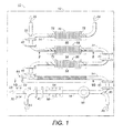
- Fig. 1 shows schematically some components of analyzer 10 on support structure 12, a fluidic structure.
- support structure 12 defines serpentine channel 14 through which an object 16 can travel, carried by a fluid or other appropriate substance.
- Object 16 can, for example, be a droplet or small volume of fluid that includes an analyte to be analyzed.
- object is used herein in the general sense of any distinguishable thing from which light can emanate, whether through emission (e.g. radiation, fluorescence, incandescence, luminescence, etc.), scattering (e.g. reflection, deflection, diffraction, refraction, etc.), or transmission.
- emission e.g. radiation, fluorescence, incandescence, luminescence, etc.
- scattering e.g. reflection, deflection, diffraction, refraction, etc.
- the light "emanates from” or is simply "from” the object.
- a droplet or small volume of fluid may, for example, include atoms, molecules, or other particles that emit light spontaneously or in response to excitation; a particle could fluoresce in response to excitation.
- a droplet may include particles that absorb light incident on the droplet, so that the droplet does not reflect or otherwise scatter the absorbed light.
- a droplet may include particles that scatter light incident on the droplet in a way that depends on photon energy, so that the droplet scatters the incident light correspondingly.
- An analyte i.e. a chemical species being investigated
- in a droplet can act as a fluorescent, absorbent, or scattering component.
- Object 16 enters channel 14 carried by a primary fluid illustrated by arrow 20, and can enter from a supply reservoir and a sample well, with its entry into the primary fluid controlled by metering electrodes 22. Rather than electrical metering, as with electrodes 22, pressure metering could be used. Other techniques could provide a droplet or other small object to channel 14.
- Analyzer 10 could be implemented with any appropriate number of channels similar to channel 14, and with each channel receiving analyte samples from a respective sample well. Furthermore, each of the channels could have a different combination of components suitable to a specific type of analysis such as fluorescence spectroscopy, laser-induced fluorescence spectroscopy (LIF), absorption spectroscopy, excitation spectroscopy, Raman scattering, surface-enhanced Raman scattering (SERS), far-infrared spectroscopy, etc. Each sample well could continuously collect a specific analyte for stationary or post-detection schemes. The channels could be formed by subdividing a broad channel into several parallel channels.
- LIF laser-induced fluorescence spectroscopy
- SERS surface-enhanced Raman scattering
- Additional fluid to carry object 16 may enter as shown by arrow 24, such as to permit a constant flow rate or consistent flow independent of the analyte supply.
- the path followed by the fluid in channel 14 can be controlled through a number of devices.
- the fluid, together with object 16 if appropriately positioned can be purged at two outlets as illustrated by arrows 26 and 28 through toggling of valves 30 and 32, respectively, each of which is at a bifurcation junction,
- Other types of gates could be used; charged particles could be deflected by Coulomb force, and polarizable particles could be deflected by dielectrophoretic force.
- Fluid can also be purged at a final outlet from channel 14, illustrated by arrow 34.
- the flow of the fluid can be maintained by conventional propulsion components such as electro-osmotic pumps 40 or some suitable hydraulic pressure pump appropriately positioned along the length of channel 14.
- propulsion components such as electro-osmotic pumps 40 or some suitable hydraulic pressure pump appropriately positioned along the length of channel 14.
- propulsion components could be used, including, for example, gas pressure pumps, positive displacement pumps, micro-peristaltic pumps, electro-kinetic pumps, piezo pumps, and thermal mode pumps.
- propulsion components can also perform system flush and initial fluid loading functions, with pressure driven techniques. Appropriate circuitry can coordinate the various pumps and other components to work in a synchronized manner.
- Coulter counter 50 and Mie scatter sensor 52 are conventional sensing components, illustratively along parts of one straight portion of channel 14.
- Coulter counter 50 is an example of an electrically based particle size detector.
- Mie scatter sensor 52 is an example of an optical detector that relies on particle-induced scattering of light entering from the side of channel 14.
- Coulter counter 50 can be implemented to size particles in the 1-10 ⁇ m range within a continuous liquid stream.
- the Coulter counter technique should also work for other particle sizes as long as the inner diameter of channel 14 in the sensing region is not more than an order of magnitude larger than the particles being measured.
- the series of sensing components also includes optical (e.g. visible or infrared) absorption sensing component 54, first fluorescence sensing component 56, second fluorescence sensing component 58, and Raman scatter sensing component 60.
- Analyzer 10 could include any other suitable combination of sensing components, including some that are not connected in series. Additional sensing components could include conventional optical or electrical trigger elements that provide a signal indicating when an analyte with properties meeting certain criteria moves past a position along channel 14. Furthermore, it may be possible to include sensing components for electrical impedance spectroscopy (EIS) for electronic pathology rather than sensing differential resistance for bioparticle sizing.
- EIS electrical impedance spectroscopy
- a series of sensing components as in Fig. 1 makes it possible to obtain spectral information about moving particles or other objects in order to achieve orthogonal characterization and reliable identification. Characterization is orthogonal if sensing components obtain information about orthogonal characteristics of a moving object, such as by photosensing different ranges of photon energies; sensing components could also be suitable for different intensity ranges. By choosing suitable materials, it is possible to obtain spectral information for the entire range from the deep ultraviolet to the far infrared or even for frequencies in the THz range.
- Analyzer 10 can be designed to perform multi-signal analysis for a specific application, whether high wavelength resolution or broadband detection is desired.
- the technique illustrated in Fig. 1 also takes advantage of the motion of object 16 with a geometry that enables long integration times without sacrificing throughput capacity.
- Highly sensitive optical characterization methods can be used, such as fluorescence spectroscopy (illustratively in more than one range of photon energies) and Raman spectroscopy.
- fluorescence spectroscopy illustrated in more than one range of photon energies
- Raman spectroscopy Raman spectroscopy
- Each of sensing components 54, 56, 58, and 60 includes a respective one of ICs 64, 66, 68, and 70.
- Each of these ICs includes a photosensor array, and the sensing component includes a set of cells of the photosensor array.
- the set of cells photosenses photons within a range of photon energies.
- more than one IC, such as ICs 66 and 68, could photosense fluorescing photons that are in the same energy range, but that result from excitation at different wavelengths such as from different LED or laser light sources.
- the set of cells for each of sensing components 54, 56, 58 and 60 includes a subset of cells, each of which photosenses in a respective subrange, and the subranges of at least two of the cells are different from each other.
- Sensing components 56, 58, and 60 can each be implemented with any suitable excitation or illumination technique to cause emanation of light from objects. Enhanced light-target interaction is especially important if analyzer 10 is characterizing single particles or low concentrations of biological or chemical agents.
- ICs 66, 68, and 70 are supported on spacers 72, providing a suitable gap between each IC and the respective portion of channel 14 to avoid interference with anti-resonant waveguiding.
- Suitable configurations and resonant waveguide techniques can include an aerosol in a glass capillary tube or a liquid film between glass slides.
- the excitation could be with any appropriate electromagnetic radiation.
- Additional background suppression of excitation light can be obtained using a wavelength filtering component as part of the wall of channel 14 or as an additional coating on top of a photosensor array.
- Fig. 2 shows schematically a cross-section of analyzer 10 taken along the line 2-2 in Fig. 1. Similar features would be found in first fluorescence sensing component 56 and, to an extent, in Raman scatter sensing component 60.
- portion 80 of channel 14 As object 16 travels through portion 80 of channel 14 in the downstream direction indicated by arrow 82, it receives light from an excitation component, illustratively light source 84 which could be a laser or an LED, for example.
- Portion 80 can function as an anti-resonant waveguide in response to light from source 84, or it can function in another way that provides enhanced light-target interaction.
- other techniques that provide continuous excitation to a fluorescing molecule include tracking the molecule in motion with a scanning laser beam; using a linear array of LEDs to sustain particle excitation along its path; arranging a collimated beam along the particle path without waveguiding; and providing a Fabry-Perot-style cavity in which light passes through the medium containing the particle several times.
- Sensing components using anti-resonant waveguide modes are especially advantageous in combination with fluidic devices because the fluidic channels themselves can be used as anti-resonant waveguides in various configurations. Examples of configurations include an aerosol carrying analytes in a capillary, a liquid film carrying analytes within a channel or between glass slides, etc.
- an analyte within object 16 fluoresces, emitting light with a characteristic spectrum of photon energies.
- a portion 86 of the light is emitted toward assembly 87, which includes at least !C 68 and possibly also other structures. Photons in portion 86 can therefore be photosensed by cells of a photosensor array on IC 68.
- Assembly 87 is positioned so that the photosensor array on IC 68 is close to and parallel to the path of object 16 through portion 80, to increase light collection efficiency.
- Assembly 87 is illustratively supported on spacers 72 to avoid disturbing anti-resonant waveguiding in portion 80 of channel 14.
- Spacers 72 are positioned outside portion 80, and, as a result, air gap 88 below assembly 87 prevents disturbance of waveguiding because air has a lower refractive index than that of the liquid within the waveguide.
- a thin gap, layer, or film that is only a few microns thick, e.g. 10 ⁇ m, is sufficient to prevent disturbance of waveguiding if it has a sufficiently low refractive index.
- the structure shown in Fig. 2 could also be used to implement Raman scatter sensing component 60 in a way that, although not comparable to dedicated Raman sensors, may provide acceptable performance and resolution with sufficient spectral range for a given application such as for specific Raman bands of interest.
- the output signal could indicate a set of intensity ratios of selected Raman lines and/or certain narrow intervals of a Raman spectrum rather than a complete Raman spectrum.
- this technique could provide the most relevant input for data analysis and comparison against a library of Raman profiles or another such database. This approach may be more tractable and efficient as a first step than comparing an entire Raman spectrum with a huge library of profiles.
- a fluorescence sensing component could include a photosensor array in which cells photosense within a wide spectral range with rather low resolution, e.g. 400-700 nm with a moderate wavelength resolution of 2-5 nm.
- a Raman scatter sensing component could include a photosensor array in which cells photosense within a smaller spectral range close to the excitation wavelength but with greater resolution, e.g. 800-830 nm with a resolution of 0.2-0.5 nm or even higher resolution.
- Fig. 2 also illustrates one of the ways in which support structure 12 could be implemented.
- Support layer 90 could, for example, be a light-transmissive glass or silicon substrate.
- Channel 14 can be defined in a micromolded layer 92 of polydimethylsiloxane (POMS).
- POMS polydimethylsiloxane
- Techniques for producing a patterned layer of PDMS include, for example, fabricating a template on glass from SU-8 polymer, and then depositing PDMS to form a patterned structure within the template. The template can then be removed.
- a light-transmissive plate 94 such as glass.
- channels could be microfabricated by patterning a layer of a polymer material such as SU-8 to produce high aspect ratio channel walls. Depending on the medium that carries analyte through channel 14, parameters of channel 14 can be modified for optimal results.
- a specific parameter of channel 14 that can have significant effects is adhesiveness of the channel wall.
- an anti-adhesive coating can be applied to prevent bioparticles and other analytes from sticking to the walls.
- Dip-coated polyethylene glycol (PEG) is a good choice for preventing adhesion of most biomaterials and can maintain capillary force on aqueous solutions.
- Other coatings may be viable options, such as parylene C or vapor deposited tetraglyme.
- Fig. 2 also shows optical component 96 on the side of support layer 90 opposite PDMS layer 92.
- Optical component 96 provides an appropriate surface 98 through which light from source 84 can be coupled into the anti-resonant waveguide within portion 80 of channel 14.
- support layer 90 and optical component 96 could instead be fabricated from a single layer of material by suitable processes.
- Fig. 3 is a schematic view of an implementation of assembly 87 in which IC 68 includes photosensor array 100 and also has spacers 72 attached to it.
- Photosensor array 100 is illustratively a two-dimensional array, with at least two rows of cells that include photosensors.
- photosensor array 100 can be provided with different coatings or can be otherwise structured so that their cells photosense different ranges or subranges of photon energies. As a result, the information obtained from a single IC can provide a detailed analysis of incident photons over a broad range of photon energies.
- reference cells such as the cells in row 102, can be used to provide a spatially resoled real-time reference signal.
- a feature of array 100 is that it includes one or more reference cells that are nearby to a subrange cell.
- Each cell in row 102 photosenses photons throughout a suitable range, characterized as ⁇ all , to produce a reference for a nearby cell in row 104.
- the cell in row 102 must be different from the cells in row 104. For example, it could have a different sensing area or it could have a gray filter coating different than a coating over the paired cell in row 104.
- Each cell in row 104 photosenses a respective subrange between ⁇ min and ⁇ max , with illustrative cell 106 photosensing a subrange centered around ⁇ p .
- IC 68 also includes array circuitry as well as peripheral circuitry 110 which perform various functions relating to readout of photosensed information from array 100.
- IC 68 provides a compact photosensor array that can be used for various functions within a system such as analyzer 10.
- the compactness of IC 68 also allows for an interactive detection scheme. Subsequent or adjacent ICs within analyzer 10 may exchange information or trigger events. The combination of analysis results from several ICs within analyzer 10 may help to obtain orthogonal information and ultimately enable reliable identification of object 16.
- Fig. 4 illustrates another implementation of assembly 87, showing in greater detail how cells of an array photosense subranges. Assembly 87 as in Fig. 4 can be supported over air gap 88 by spacers 72.
- a cross-section has been taken through a fragment 150 of a photosensor array, with cells 152 of the fragment 150 shown schematically in cross-section.
- a transmission structure 160 that receives incident light 162, such as from an optional Selfoc® or other gradient index (GRIN) lens array, illustrated by lens array portion 164.
- Lens array portion 164 can be designed to receive light from air gap 88 as in Fig. 2 and to provide a parallel beam to structure 160, increasing spectral resolution,
- Transmission structure 160 can be a film with laterally varying light transmission properties.
- wedge-shaped transmissive cavity 170 is enclosed between reflective films 172 and 174, forming a wedge-shaped Fabry-Perot etalon. Because its thickness varies as a function of position along the x-axis, transmission structure 180 will transmit different wavelengths as a function of position along the x-axis,
- Transmission structure 160 can be produced with appropriate coatings on or over a photosensor array.
- Films 172 and 174 and cavity 170 could all be produced by exposure to deposition beams in an evaporation chamber: uniform thicknesses could be produced by appropriate on-axis deposition, while laterally varying thickness can be produced by appropriate off-axis deposition.
- Fig. 4 illustratively shows films 172 and 174 as relatively thick compared to cavity 170, which would be appropriate for layers of non-metallic material such as SiO 2 , TiO 2 , or Ta 2 O 5 . If films 172 and 174 are reflective metal, however, they could be much thinner.
- cavity 170 and films 172 and 174 could be designed from the desired transmitted wavelength ⁇ and the refractive index n of cavity 170.
- the thickness of cavity 170 is typically chosen to be ⁇ /(2n) or an integer multiple thereof, while the thicknesses of Bragg mirror layers within films 172 and 174 are typically ⁇ /(4n).
- the number of pairs of such layers in each of films 172 and 174 can vary between a few (e.g. 2-5) all the way up to 20 or 30, depending on the difference in refractive index between the two materials used, the desired transmission band width, and the desired stop band reflectivity. Therefore, in typical implementations, films 172 and 174 are much thicker than cavity 170.
- Fig. 5 illustrates the laterally varying light transmission properties of transmission structure 160. Because its thickness varies as a function of position along the x-axis, cavity 170 transmits different wavelengths as a function of position along the x-axis. Wavelengths of photons predominantly transmitted to nine of cells 152 as in fragment 150 are illustrated by the low reflectivity minima labeled 1 through 9. The high-transmissivity photon energy range for transmission structure 160 varies laterally.
- Assembly 87 includes transmission structure 180.
- Transmission structure 180 can be a laterally graded Bragg mirror in which each of layers 182, 184, 186, and 188 is laterally graded.
- layers 182, 184, 186, and 188 could be produced as described above for cavity 170.
- Fig. 7 illustrates the laterally varying light transmission properties of transmission structure 180.
- Transmission structure 180 reflects different wavelengths as a function of position along the x-axis. Curves 200, 202, 204, and 206 are shown, representing reflectivity of the portion of transmission structure 180 over each of four cells 152 in fragment 150, with curve 200 being for the leftmost cell of the four in Fig. 6 and curve 206 being for the rightmost cell of the four.
- the high-reflectivity photon energy range for transmission structure 180 varies laterally.
- Fig. 8 illustrates a technique that produces transmission structure 210 with laterally varying light transmission properties similar to those illustrated in Figs. 5 and 7 but with lateral variation in each of two dimensions.
- Transmission structure 210 is produced on or over cells 152 of photosensor array 150 by using deposition source 212 to provide deposition beam 214 that can be characterized at any given point on the surface of structure 210 by two angles, One of the two angles results from angular variation of deposition beam 214 in the x-direction across array 150, while the other results from angular variation in the y-direction.
- the thickness gradient of structure 210 is similarly different in the x- and y-directions. Therefore, cells within each row extending in one of the two directions will photosense a range of photon energies similarly to Fig. 7, but the range will be different than the range photosensed by cells in any other row extending in the same direction.
- Fig. 8 could be implemented in a variety of ways.
- structure 210 could be formed on a support structure that is tilted as required, deposition source 212 could be tilted as required, or both kinds of tilt could be employed.
- Fig. 9 illustrates a technique that produces transmission structure 220 with laterally varying light transmission properties but without variation in thickness of transmission structure 220.
- the technique in Fig. 9 can be characterized as providing laterally varying optical thickness d*n, where d is thickness and n is index of refraction, but without actual variation in thickness d.
- homogeneous coating 222 is deposited by deposition source 224, which provides deposition beam 226 uniformly over the surface of photosensor array 150.
- light source 230 provides radiation 232 that is scanned across the coating over array 150 to introduce a laterally varying change of refractive index in resulting transmission structure 220.
- source 230 can be an ultraviolet source that provides intensity I with a constant value along each line parallel to the y-axis (perpendicular to the plane of Fig. 9), but varying from I min for lines nearer the y-axis to I max for lines farther from the y-axis.
- the wavelengths transmitted to cells in array 150 can vary along the x-axis from ⁇ min to ⁇ max , as shown.
- the same pattern of intensity can be concurrently applied by source 230 to each of a number of arrays that are appropriately arranged, allowing batch fabrication of arrays. Two-dimensional variation could also be obtained.
- the resolution of a technique as in any of Figs. 4-9 depends heavily on the number of cells in an array, the full width half maximum (FWHM) of the transmission peak, and the peak shift per cell.
- the totally covered spectral width can be enhanced by increasing the FWHM and the peak shift per cell. Therefore, the technique can be customized to the needs of a specific application.
- the use of a Fabry-Perot cavity as in Fig. 4 enables very high spectral resolution, while a version with multiple cavities and many layers as in commercially available products will be favorable for applications with low light intensities in combination with small spectral resolution such as with fluorescence.
- the spectral width of the transmission window and the reflectivity of the stop band can be optimized separately, which may be advantageous because the reflectivity of the stop band determines stray light suppression. It would also be possible to use a single laterally graded distributed Bragg reflector (DBR) mirror as in Figs. 6 and 7 to obtain a photosensor array with high light sensitivity but limited wavelength resolution, appropriate for fluorescence or luminescence sensing.
- DBR distributed Bragg reflector
- the photocurrent in each cell is slightly different from its neighbors depending on the incident light spectrum. If the transmission properties of the DBR over each cell are known, the original spectrum of incident light can be reconstructed. The number of cells defines the number of spectral points that can be reconstructed and therefore determines spectral resolution. The reconstruction works best for wavelengths where transmission changes drastically from one cell to the next.
- a particular advantage of analyzer 10, when implemented with techniques similar to those of Figs. 3-9, is that spectral information of objects can be collected step-by-step as the objects move across or along a series of sensing components, each of which obtains information about a respective range of photon energies.
- highly sensitive optical characterization techniques can be combined, including multiple range fluorescence spectroscopy and Raman spectroscopy, as described above in relation to Fig. 1,
- Each of sensing components 56, 58, and 60 can be thought of as a chip-size spectrometer that includes a photosensor array together with a laterally varying filter such as a coating. The laterally varying transmission and reflection properties of the coating over the photosensor array define a correlation between position and photon energy.
- the spatially dependent signal from the photosensor array contains information about the incident spectrum. Because of the distributed nature of the spectrometer and the fact that the incident light traverses the photosensor array in the process of resolving spectral distribution, sensitivity is improved, making additional optics unnecessary.
- a coating as in Fig. 4 typically transmits approximately 60% of photons in its respective subrange.
- the subranges can be chosen with wavelengths that span between 0.01 and tens of nanometers (nm), depending on the design and gradient of the coating and the cell size of the photosensor array.
- Very high light yield can be achieved by using a highly sensitive photosensor, such as an avalanche photosensor array.
- any coating or other transmission structure over row 102 in Fig. 3 must function as a gray filter across the range ⁇ all in order to provide a suitable reference. It may also be possible to leave row 102 uncoated in some implementations.
- Fig. 10 shows schematically a cross-section of analyzer 10 taken along the line 10-10 in Fig. 1.
- Fig. 10 therefore shows several features of optical absorption sensing component 54, including IC 64.
- portion 240 of channel 14 As object 16 travels through portion 240 of channel 14 in the downstream direction indicated by arrow 242, it receives light from an excitation component, illustratively light source 244 which is a suitable broadband illumination component such as a white light source and which could be an LED or a halogen lamp.
- an excitation component illustratively light source 244 which is a suitable broadband illumination component such as a white light source and which could be an LED or a halogen lamp.
- portion 240 can function as an anti-resonant waveguide in response to light from source 244, or it can function in another way that provides enhanced light-target interaction.
- object 16 In response to light from source 244, object 16 scatters or absorbs light, resulting in a modified spectral distribution of transmitted light photosensed by cells of a photosensor array on IC 64.
- Object 16 may contain an analyte that absorbs photons within certain energy subranges, producing an absorption spectral distribution. Because object 16 receives excitation continuously throughout portion 240, cells on IC 64 will continue to photosense the absorption spectral distribution as object 16 passes through portion 240 of channel 14. Then, the spectral distribution will return to its unmodified form when object 16 exits from sensing component 54 through curved portion 246 of channel 14.
- Fig. 11 shows schematically a cross-section of analyzer 10 taken along a line similar to that of Fig. 10 but through a Raman backscatter sensing component. Many features of Fig. 11 are implemented the same as in component 54. For example after entering through curved portion 250 of channel 14, object 16 travels through portion 240 in the downstream direction indicated by arrow 242 and receives light from an excitation component, illustratively light source 244 as in Fig. 10. Portion 240 can function to provide enhanced light-target interaction, as described above.
- object 16 In response to light from source 244, object 16 (or an analyte in it) performs Raman scattering of light in an upstream direction.
- the backscattering results in a modified spectral distribution photosensed by cells of a photosensor array on an iC within assembly 252, illustratively positioned at the upstream end of portion 240 of channel 14, but alternatively positioned outside the downstream end if source 244 illuminates portion 240 from the downstream end.
- Assembly 252 could be implemented with any appropriate structure. Because object 16 receives excitation continuously throughout portion 240, cells on the IC in assembly 252 will continue to photosense the backscattered spectral distribution as object 16 passes through portion 240 of channel 14. Then, the spectral distribution will return to its unmodified form as object 16 exits. As shown, the photosensor array of the IC in assembly 252 covers the whole end facet of channel 14, including the channel walls.
- Fig, 12 illustrates a variation on Figs. 10 and 11.
- the technique of Fig. 12 can be used where channel 14 has an inner diameter less than 30 ⁇ m or is otherwise so small or so structured that light is not satisfactorily distributed over IC 64 and the IC in assembly 252 when attached directly.
- Prism 260 can be positioned to diffract light that emerges from the end facet. The diffracted light can then be photosensed by cells of array 262, with different cells photosensing different photon energy subranges. For example, ray 264 represents shorter wavelengths, ray 266 represents intermediate wavelengths, and ray 268 represents longer wavelengths, with each ray being detected by a different cell of array 262.
- Fig. 13 illustrates exemplary operations in producing an analyzer like analyzer 10 in Fig. 1.
- the operation in box 270 in Fig. 13 produces a fluidic structure with a channel in which objects can be carried by fluid.
- the operation in box 270 could include manufacturing a fluidic structure by positioning or otherwise producing a structured spacer layer between two quartz slides.
- the spacer layer could be a patterned layer of PDMS or could be any other suitable material or combination of materials, including, for example, Gelfilm® or quartz.
- the operation in box 270 could alternatively be implemented in various other ways, such as by defining a fluidic channel in a quartz slide by glass etching or by molding PDMS to produce a channel, and by then combining the resulting structure with an upper quartz slide.
- Two layers of PDMS could be fabricated on separate substrates and then one could be flipped over and aligned with the other by chip-on-chip assembly.
- a final substrate of glass, PCB, or PDMS or sufficient hardness could be used to allow direction connection to control and detection measurement circuitry.
- the operation in box 272 then attaches fluidic components to the fluidic structure produced in box 270.
- the fluidic components attached in box 272 can be operated to cause and control movement of objects in the channel.
- the operation in box 274 attaches components for enhanced light-target interaction.
- the operation in box 274 can attach optical component 96 on the side of support layer 90, providing an appropriate surface through which light can be coupled into a portion of channel 14 that functions as an anti-resonant waveguide.
- the operation in box 274 can produce spacers 72 to provide a suitable gap that avoids interference with anti-resonant wave guiding.
- the operation in box 280 attaches photosensor arrays with cells that photosense in different subranges.
- the operation in box 280 can be implemented by attaching detector 87.
- the detector can also include reference cells.
- each light source can be attached once, after which it is stationary, In the operation in box 282, one or more light sources are positioned to produce excitation of objects being carried within the channel.
- Fig. 13 could be modified.
- the operations in boxes 272, 274, 280, and 282 could be combined in any appropriate way to facilitate attachment of components in a desired sequence.
- an additional operation could be performed to align or attach interconnects between ICs, gates, and other circuitry, such as connectors to a microprocessor or computer, or this operation could be partially performed in each of boxes 272, 274, 280, and 282.
- Fig. 14 shows an alternative arrangement that could be produced by an implementation of Fig. 13.
- First and second fluorescence sensing components 56 and 58 are next to each other in the series of sensing components along channel 14. In addition, however, they are positioned so that IC 290 can be attached over both of them.
- the photosensor array of IC 290 includes both cells along channel 14 within component 56 and also cells along channel 14 within component 58.
- Fig. 15 is a cross-section along the line 15-15 in Fig. 14, and shows how detector 292 which includes IC 290, can be supported over air gap 88 by spacers 72.
- the lateral variation in optical thickness of the transmission structure may be such that the ranges and subranges photosensed within sensing component 56 are different from those photosensed within sensing component 58; alternatively, the ranges and subranges could be the same.
- Spacers 72 can help to reduce cross-talk between components 56 and 58 because spacers 72 can be shaped and positioned to act as light-absorbing walls between the two components.
- Fig. 16 shows an alternative arrangement in which detector 292 as in Fig. 15 is positioned over a set of parallel channels 294, which could be produced by producing walls 296 to subdivide a larger channel into subchannels. Laterally varying optical thicknesses of a transmission structure can be produced so that a different range of photon energies is photosensed in each of channels 294, or different subranges are photosensed in different channels, or the same ranges and subranges could be photosensed in all channels.
- Fig. 17 shows an alternative arrangement that could be produced by an implementation of sensing component 58 in Fig. 2, with components similar to those described above in relation to Fig. 2 having the same reference numerals.
- portion 80 of channel 14 functions as an anti-resonant waveguide in response to light from source 84.
- Assembly 87 is along portion 80, separated from plate 94 by spacers 72. Upstream from portion 80 (but downstream from light source 84) can be positioned a series of triggering photodetectors, represented by photodetector 300 on spacers 302.
- fluorescing objects 310, 312, and 314 are being carried through channel 14. As they fluoresce, objects 310, 312, and 314 emanate photons, represented respectively by rays 320, 322, and 324.
- Fig. 18 illustrates system 400 that can operate analyzer 10.
- System 400 illustratively includes central processing unit (CPU) 402 connected to various components through bus 404..
- CPU central processing unit
- System 400 also includes external input/output (I/O) component 406 and memory 408, both connected to bus 404.
- I/O 406 permits CPU 402 to communicate with devices outside of system 400.
- IC I/O 410 is a component that permits CPU 402 to communicate with ICs in analyzer 10; M ICs are illustrated in Fig. 18 by a series extending from IC(0) 412 to IC (M-1) 414. ICs 412 through 414 illustratively include IC(m) 416 with a photosensor array 418, which includes cells that photosense subranges as described above.
- fluidic device I/O 420 is a component permitting CPU 402 to communicate with various fluidic devices; N fluidic devices are represented in Fig. 18 by device (0) 422 through device (N-1) 424.
- Memory 408 includes program memory 430.
- the routines stored in program memory 430 illustratively include relative movement routine 440, detect, readout, and combine routine 442, and object selection routine 446.
- CPU 402 executes relative movement routine 440 to communicate with fluidic devices 422 through 424.
- CPU 402 can receive signals from sensors, perform computations to determine what fluidic operations are necessary, and then provide signals to activate pumps, metering electrodes, gates, and valves to produce appropriate relative movement between objects in channel 14 and photosensor arrays along channel 14.
- CPU 402 can call a subroutine implemented as shown in Fig. 19, which could instead be within routine 442.
- the subroutine in Fig. 19 can be implemented for single objects moving past arrays or for spaced multiple objects moving past arrays, provided the spacings between objects are sufficient to avoid interference.
- CPU 402 executes the operation in box 480, it performs a pre-sensing readout.
- the information could be obtained from a series of photodetectors illustrated by photodetector 300 in Fig. 17 or from reference cells in the photosensor array, such as the cells in row 102 in Fig. 3. It would also be possible to modify the photosensor array to include trigger cells positioned along channel 14 upstream from a line of subrange cells, and uncoated so that they provide information about all photon energies.
- CPU 402 can obtain information about each object and determine an appropriate sensing period for each object, in the operation in box 482. For example, CPU 402 could perform calculations to determine whether one or more objects are present, the position of each object, and the speed of each object. Using this information and taking into account previously calculated sensing periods for the same objects, if any, CPU 402 can also determine an appropriate sensing period to be used during sensing readout; in general, the sensing period must provide an integration time shorter than the time necessary for an object to pass each subrange cell. Each object can therefore have a unique sensing period. Alternatively, CPU 402 could provide signals to adjust fluid speed to obtain the same result.
- CPU 402 can then perform the sensing readout operation, in box 484.
- This operation includes providing signals so that photons are photosensed cumulatively during the sensing period obtained in box 482, and may also include signals to peripheral circuitry on an IC so that analog quantities photosensed by subrange cells are adjusted based on analog quantities sensed by paired reference cells. After adjustment, if any, analog quantities can be converted to digital signals for readout.
- the photosensed quantities read out in box 484 can also be digitally adjusted by CPU 402 before being stored for each object, in box 490.
- the digital adjustment can include adjusting quantities photosensed by subrange cells based on quantities photosensed by paired reference cells.
- the position and speed information about each object from box 482 can be used to determine which photosensed quantities result from photons emanating from each object.
- CPU 402 can employ data structures stored in memory 408. For example, one data structure can store each object's previously calculated position and speed, which can then be used in performing subsequent calculations to identify the same object. Also, a readout data structure can be employed to hold all of the adjusted quantity information about each object. The operation in box 490 can update the readout data structure each time it obtains additional information about the same object. In an implementation as in Fig. 18, the operations in boxes 480, 482, 484, and 490 can be performed separately for each of ICs 412 through 414. Further, as suggested by the dashed line from box 490 to box 480, the same operations can be performed repeatedly for each of the ICs.
- each object's optical signal may move only a few cells along the photosensing path, and consecutive objects must be sufficiently separated to avoid confusion.
- Objects could be closer together. Even if several objects are emanating photons to the same cell at the same time, it may be possible to separate the signals of the objects. Similarly, if objects are very close to each other but positioned along different cells, an optical structure between channel 14 and detector 87 could ensure that photons emanating from different objects travel to different cells. Furthermore, techniques as described above could be applied to a continuous fluidic stream without distinguishable objects in it, in which case the optical signal emanating from the stream would be determined by concentrations of molecules in each position in the stream.
- CPU 402 can perform the operation in box 492 to provide photosensed quantities. As shown, this operation can include combining the sensed quantities for each object so that spectral information about the object can be provided.
- Fig. 20 illustrates an example of how object selection routine 446 in Fig. 18 could be implemented, using spectral information provided by the operation in box 492 in Fig. 19.
- Routine 446 begins with the operation in box 520, which coordinates routines 440 and 442 as described above, obtaining spectral information from the operation in box 492.
- the operation in box 522 receives the spectral information from box 520, such as in the form of a profile or other data structure.
- the operation in box 522 then compares the spectral information with other information to obtain a comparison result.
- the other information used in the comparison could be stored in a library of profiles or other database within memory 408, or could be embedded within routine 446. Any appropriate comparison technique could be used.
- the result of the comparison will indicate whether the object is appropriate for further operations within analyzer 10.
- the operation in box 530 branches based on whether the object is a candidate for further operations. If not, the operation in box 532 opens a smart gate or provides appropriate control signals to perform another operation to purge the object from the active analysis channel in analyzer 10. But if the object is appropriate for further operations, the operation in box 534 ensures that the smart gate is closed or provides control signals for other suitable operations to transfer the object downstream within the active analysis channel so that a more refined analysis or a more detailed analysis can be performed.
- the exemplary implementations described above can provide compact, inexpensive components that generally require no additional mechanical or optical parts to perform functions such as spectrometry.
- the results of photosensing can be read out rapidly and in parallel from a number of ICs, allowing fast data acquisition; as a result, an initial characterization of an object may be used to determine whether to perform more refined or detailed analysis of the object, or to determine which of different types of analysis are performed.
- a multi-signal approach like this is compatible with reagentless identification; also, a wide variety of objects can be identified in a wide variety of fluids.
- Spectrometry measurements have a wide variety of applications, including, for example, optical instrumentation, telecommunications, fluorescence devices, process control, optical signal scanning, detection systems for chemical and biological agents, and so forth.
- An example of a specific application is an in-line detector for manufacturing and functionalizing colloidal particles in an industrial setting.
- processes typically are performed in dosed systems and the properties of colloidal particles can be assessed only after all processing steps are completed.
- a small detection platform implemented as described above can be easily built into an on-line detector directly connected to a manufacturing vessel. As a result, small amounts of particles can be analyzed continuously in real time to determine size, chemical composition, and surface conditions. This approach permits instant process adjustments leading to production of materials with consistent properties from run to run.
- In-line Coulter counters for instant size measurements are already commercially available, but compact detectors as described above can also probe chemical composition using multiple advanced spectroscopic methods, an approach not previously available.
- Components could have various other shapes, dimensions, or other numerical or qualitative characteristics.
- photosensor arrays for a desired speed, sensitivity and wavelength range could have any suitable material, such as silicon, germanium, indium-gallium-arsenide, gallium arsenide, gallium nitride, or lead sulphide, and could be produced with any appropriate kind of devices, including, for example, photodiodes, avalanche photodiodes, p-i-n diodes, photoconductors, and so forth, with any appropriate technique for sensing and reading out information whether based on CCD, CMOS, or other techniques.
- Various commercially available detector arrays have pixel densities as high as ten megapixels, and some high density ICs have become relatively inexpensive.
- transmission structures could be fabricated with any appropriate techniques, including thin film technology such as sputtering, e-beam or thermal evaporation with or without plasma assistance, epitaxial growth, MBE, MOCVD, and so forth.
- appropriate pairs of materials with low absorption coefficients and large difference in refractive indices could be chosen, bearing in mind the photon energies of interest; exemplary materials include SiO 2 /TiO 2 , SiO 2 /Ta 2 O 5 , GaAs/AlAs, and GaAs/AtGaAs. Thicknesses of layer in transmission structures may vary from 30 nm up to a few hundred nanometers.
- Some of the above exemplary implementations employ an arrangement of ICs relative to fluidic structures, and a wide variety of such arrangements could be made.
- the invention could also be implemented with any other suitable type of photosensor array, including simple light-to-electric signal transducers arranged as cells of a photosensor array.
- the techniques described above allow concurrent photosensing of multiple objects.
- a preliminary inspection of an analyte could be made with an IC with a 400-700 nm laterally varying filter to detect fluorescence or scattering in the 400-700 nm range, after which a more refined inspection could be made with another IC, such as to perform Raman spectroscopy in the range of 100 cm -1 to a few 1000 cm -1 .
- Different rows of a single two-dimensional photosensor array on an IC could be differently coated to photosense in different ranges.
- Some of the above exemplary implementations employing fluidic structures also employ enhanced light-target interaction to obtain fluorescence.
- the techniques described above could also be used for self-emitting or auto-fluorescing objects such as particles.
- various types of fluorescence, photo-luminescence, chemo-fluorescence, inelastic scattering, and so forth could be employed.
- the technique of anti-resonant waveguiding, described above is only one of many techniques that could be used for enhanced light-target interaction, and any such excitation technique could be applied continuously or intermittently along a path.
- Various parameters could be adjusted to obtain anti-resonant waveguiding, including the shape of quartz or glass surrounding the channel; a thinner structure is generally better, with a surface parallel to the channel generally being required.
- a CPU which could be a microprocessor or any other appropriate component.
- routines as described above in relation to Figs. 18-20 could be done either on the same IC as a photosensor array, on other components, or on a combination of the two, with any appropriate combination of software or hardware.
- the above exemplary implementations generally involve production and use of various components following particular operations, but different operations could be performed, the order of the operations could be modified, and additional operations could be added.
- the transmission structure could be moved relative to the photosensor array between consecutive sensing operations.
- readout of adjusted or unadjusted sensed quantities from an IC could be performed serially or in parallel, and could be performed cell-by-cell or in a streaming operation.
Abstract
Description
- The present invention relates to sensing photons emanating from objects in channels.
-
U.S. Patent No. 6,580,507 describes a multiple-longitudinal flow cell channel system in which an array detector is positioned to monitor radiation from at least two of multiple flow cell channels, at separate groupings of pixels on the detector. - In accordance with a first aspect of the present invention, apparatus comprises:
- a fluidic structure with a channel defined therein within which objects travel, the objects being capable of emanating photons as the objects travel within the channel; and
- along the channel, a series of two or more sensing components that obtain information about objects traveling within respective portions of the channel; the series including a first sensing component that includes a respective set of cells of a photosensor array, the set of cells photosensing photons within a first range of photon energies that emanate from objects traveling within the respective portion of the channel, the set including a subset of two or more cells each of which photosenses photons in a respective subrange of the first range of photon energies, the subranges of at least two cells in the subset being different from each other.
- In accordance with a second aspect of the present invention, a method of obtaining information about objects comprises:
- causing one or more objects to travel within a channel defined within a fluidic structure while photons emanate from the objects; and
- using a series of sensing components along the channel, obtaining information about objects traveling within respective portions of the channel; the series including a first sensing component that includes a respective set of cells of a photosensor array, the set of cells photosensing photons within a first range of photon energies that emanate from objects traveling within the respective portion of the channel, the set including a subset of two or more cells each of which photosenses photons in a respective subrange of the first range of photon energies, the subranges of at least two cells in the subset being different from each other; the act of using the series of sensing components comprising:
- using information from the first sensing component to obtain spectral information about objects traveling within its respective portion of the channel,
- These and other features and advantages of exemplary embodiments of the invention are described below with reference to the accompanying drawings:
- Fig. 1 is a schematic diagram of an analyzer on a fluidic structure.
- Fig. 2 is a schematic cross-sectional view of the analyzer in Fig. 1, taken along the line 2-2.
- Fig. 3 is a schematic plan view of an implementation of an assembly that can be used in Fig. 2, including an integrated circuit (IC) with a photosensor array.
- Fig. 4 is a schematic cross-sectional view of another implementation of an assembly that can be used in Fig. 2.
- Fig. 5 is a graph illustrating laterally varying light transmission properties of a transmission structure in Fig. 4.
- Fig. 6 is a schematic cross-sectional view of another implementation of an assembly that can be used in Fig. 2.
- Fig. 7 is a graph illustrating the laterally varying light transmission properties of a transmission structure in Fig. 6.
- Fig. 8 illustrates a technique that produces a transmission structure that can be used in an assembly as in Fig. 2, showing orthogonal schematic cross-section views of deposition.
- Fig. 9 illustrates another technique for producing a transmission structure that can be used in an assembly in Fig. 2, showing two schematic cross-section views of stages of the technique.
- Fig. 10 is a schematic cross-sectional view of the analyzer in Fig. 1 taken along the line 10-10.
- Fig. 11 is a schematic cross-sectional view similar to that of Fig. 10 for a backscatter sensing component.
- Fig. 12 is a schematic diagram showing use of a prism in an alternative implementation to those of Figs. 10 and 11.
- Fig. 13 is a flowchart showing general operations that can be performed in producing an analyzer as in Fig. 1.
- Fig. 14 is a schematic drawing of an alternative implementation of part of an analyzer on a fluidic structure as in Fig. 1.
- Fig. 15 is a schematic cross-sectional view of the alternative implementation in Fig. 14, taken along the line 15-15.
- Fig. 16 is a schematic plan view of a portion of an alternative implementation of an analyzer as in Fig. 1.
- Fig. 17 is a schematic cross-sectional view of an alternative implementation of the sensing component in Fig. 2.
- Fig. 18 is a schematic block diagram of a system that can control the analyzer of Fig. 1.
- Fig. 19 is a flowchart showing general operations implementing a detect, readout, and combine routine as in Fig. 18.
- Fig. 20 is a flowchart showing general operations implementing an object selection routine as in Fig. 18.
- In this specification, "light" refers herein to electromagnetic radiation of any wavelength or frequency; unless otherwise indicated, a specific value for light wavelength or frequency is that of light propagating through vacuum. The term "photon" refers herein to a quantum of light, and the term "photon energy" refers herein to the energy of a photon.
- The various exemplary implementations described below address problems that arise in obtaining information about nanoparticles, microorganisms, bioagents, toxins, and other analytes, such as in aerosols, water, blood, food, and other specimens. One of those problems is the difficulty of obtaining complete spectral information about an analyte rapidly, without specially skilled personnel, and without bulky, expensive equipment as is conventionally used. The difficulty of obtaining complete spectral information is especially problematic for optical characterization of moving fluid-borne analytes that are hard to capture (or where it is not desired to capture them) so that it is necessary to obtain spectral information while they are moving.
- Other problems arise due to currently available optical characterization techniques. Optical techniques offer very high sensitivity, but discrimination remains difficult in all wavelength ranges. In addition, optical techniques for identifying analytes are constrained by weak interaction with excitation light and by the need to move a sample from one device to another if more than one detection technique is necessary for unique identification. A further complication is that bioagents dispersed either in an aerosol or in water are typically in such low concentrations that they are below the limit of detection of even the most sensitive available detection techniques; detection of low concentrations is important, because, for example, the ingestion of a single bacterium might lead to fatal consequences.
- Some have proposed orthogonal approaches that analyze combined data from a range of different optical detection techniques. Identifying particular species of bioagents is problematic but encouraging results have been obtained with current techniques. It has been shown that two-wavelength fluorescence excitation can provide good class differentiation for individual biomolecules. Class identification in the case of mixtures or in the presence of different environments still appears problematic.
- Detection techniques that use polymerase chain reaction (PCR) or specific binding of target molecules to analytes require expensive chemicals and can only be used with analytes for which target molecules are available. Such techniques are also prone to unpredicted results in messy samples contaminated with organic and inorganic dirt. Specific binding is often monitored by optical recognition techniques, such as fluorescence excitation, but this requires the analyte to be tagged with fluorophores and photo-bleaching restricts the time frame for optical probing. Other methods that do not require labeling measure small refractive index changes causing by specific binding to a probe surface; even where all conditions are right, a specifically bound monolayer is typically very thin (less than 1 nm up to a few nm) and the refractive index change is very small, leading to low signal-to-noise ratios and resulting errors,
- Detection techniques that use optical biosensors, especially sophisticated versions based on Raman scattering, IR spectroscopy, or multi-wavelength fluorescence excitation, require bulky optical instruments.
- Some of the photosensing implementations described herein employ structures with one or more dimensions smaller than 1 mm, and various techniques have been proposed for producing such structures. In particular, some techniques for producing such structures are referred to as "microfabrication." Examples of microfabrication include various techniques for depositing materials such as growth of epitaxial material, sputter deposition, evaporation techniques, plating techniques, spin coating, printing, and other such techniques; techniques for patterning materials, such as etching or otherwise removing exposed regions of thin films through a photolithographically patterned resist layer or other patterned layer; techniques for polishing, planarizing, or otherwise modifying exposed surfaces of materials; and so forth.
- Fig. 1 shows schematically some components of
analyzer 10 onsupport structure 12, a fluidic structure. Defined insupport structure 12 isserpentine channel 14 through which anobject 16 can travel, carried by a fluid or other appropriate substance.Object 16 can, for example, be a droplet or small volume of fluid that includes an analyte to be analyzed. - The term "object" is used herein in the general sense of any distinguishable thing from which light can emanate, whether through emission (e.g. radiation, fluorescence, incandescence, luminescence, etc.), scattering (e.g. reflection, deflection, diffraction, refraction, etc.), or transmission. The light "emanates from" or is simply "from" the object.
- Examples of objects that could occur in implementations as described below include droplets, small volumes of fluid, single molecules, agglomerated molecules, molecule clusters, cells, viruses, bacteria, proteins, DNA, microparticles, nanoparticles, and emulsions. A droplet or small volume of fluid may, for example, include atoms, molecules, or other particles that emit light spontaneously or in response to excitation; a particle could fluoresce in response to excitation. Or a droplet may include particles that absorb light incident on the droplet, so that the droplet does not reflect or otherwise scatter the absorbed light. Or a droplet may include particles that scatter light incident on the droplet in a way that depends on photon energy, so that the droplet scatters the incident light correspondingly. An analyte (i.e. a chemical species being investigated) in a droplet can act as a fluorescent, absorbent, or scattering component.
-
Object 16 enterschannel 14 carried by a primary fluid illustrated byarrow 20, and can enter from a supply reservoir and a sample well, with its entry into the primary fluid controlled bymetering electrodes 22. Rather than electrical metering, as withelectrodes 22, pressure metering could be used. Other techniques could provide a droplet or other small object tochannel 14. - Analyzer 10 could be implemented with any appropriate number of channels similar to
channel 14, and with each channel receiving analyte samples from a respective sample well. Furthermore, each of the channels could have a different combination of components suitable to a specific type of analysis such as fluorescence spectroscopy, laser-induced fluorescence spectroscopy (LIF), absorption spectroscopy, excitation spectroscopy, Raman scattering, surface-enhanced Raman scattering (SERS), far-infrared spectroscopy, etc. Each sample well could continuously collect a specific analyte for stationary or post-detection schemes. The channels could be formed by subdividing a broad channel into several parallel channels. - Additional fluid to carry
object 16 may enter as shown byarrow 24, such as to permit a constant flow rate or consistent flow independent of the analyte supply. The path followed by the fluid inchannel 14 can be controlled through a number of devices. For example, the fluid, together withobject 16 if appropriately positioned, can be purged at two outlets as illustrated byarrows valves channel 14, illustrated byarrow 34. - The flow of the fluid can be maintained by conventional propulsion components such as electro-
osmotic pumps 40 or some suitable hydraulic pressure pump appropriately positioned along the length ofchannel 14. A wide variety of other propulsion components could be used, including, for example, gas pressure pumps, positive displacement pumps, micro-peristaltic pumps, electro-kinetic pumps, piezo pumps, and thermal mode pumps. In addition to maintaining flow of fluid, propulsion components can also perform system flush and initial fluid loading functions, with pressure driven techniques. Appropriate circuitry can coordinate the various pumps and other components to work in a synchronized manner. - Along
channel 14 is a series of sensing components, each of which obtains information aboutobject 16 as it travels within a respective straight portion ofchannel 14; the straight portions are separated by 180-degree curved portions. Coulter counter 50 andMie scatter sensor 52, for example, are conventional sensing components, illustratively along parts of one straight portion ofchannel 14.Coulter counter 50 is an example of an electrically based particle size detector.Mie scatter sensor 52 is an example of an optical detector that relies on particle-induced scattering of light entering from the side ofchannel 14. - Coulter counter 50 can be implemented to size particles in the 1-10µm range within a continuous liquid stream. The Coulter counter technique should also work for other particle sizes as long as the inner diameter of
channel 14 in the sensing region is not more than an order of magnitude larger than the particles being measured. - The series of sensing components also includes optical (e.g. visible or infrared)
absorption sensing component 54, firstfluorescence sensing component 56, secondfluorescence sensing component 58, and Ramanscatter sensing component 60.Analyzer 10 could include any other suitable combination of sensing components, including some that are not connected in series. Additional sensing components could include conventional optical or electrical trigger elements that provide a signal indicating when an analyte with properties meeting certain criteria moves past a position alongchannel 14. Furthermore, it may be possible to include sensing components for electrical impedance spectroscopy (EIS) for electronic pathology rather than sensing differential resistance for bioparticle sizing. - A series of sensing components as in Fig. 1 makes it possible to obtain spectral information about moving particles or other objects in order to achieve orthogonal characterization and reliable identification. Characterization is orthogonal if sensing components obtain information about orthogonal characteristics of a moving object, such as by photosensing different ranges of photon energies; sensing components could also be suitable for different intensity ranges. By choosing suitable materials, it is possible to obtain spectral information for the entire range from the deep ultraviolet to the far infrared or even for frequencies in the THz range.
-
Analyzer 10 can be designed to perform multi-signal analysis for a specific application, whether high wavelength resolution or broadband detection is desired. The technique illustrated in Fig. 1 also takes advantage of the motion ofobject 16 with a geometry that enables long integration times without sacrificing throughput capacity. Highly sensitive optical characterization methods can be used, such as fluorescence spectroscopy (illustratively in more than one range of photon energies) and Raman spectroscopy. The use of multi-signal analysis makes it possible to perform reagentless bioagent identification. - Each of
sensing components ICs ICs sensing components -
Sensing components analyzer 10 is characterizing single particles or low concentrations of biological or chemical agents.ICs spacers 72, providing a suitable gap between each IC and the respective portion ofchannel 14 to avoid interference with anti-resonant waveguiding. - Suitable configurations and resonant waveguide techniques can include an aerosol in a glass capillary tube or a liquid film between glass slides. The excitation could be with any appropriate electromagnetic radiation.
- Additional background suppression of excitation light can be obtained using a wavelength filtering component as part of the wall of
channel 14 or as an additional coating on top of a photosensor array. - Fig. 2 shows schematically a cross-section of
analyzer 10 taken along the line 2-2 in Fig. 1. Similar features would be found in firstfluorescence sensing component 56 and, to an extent, in Ramanscatter sensing component 60. - As
object 16 travels throughportion 80 ofchannel 14 in the downstream direction indicated byarrow 82, it receives light from an excitation component, illustrativelylight source 84 which could be a laser or an LED, for example.Portion 80 can function as an anti-resonant waveguide in response to light fromsource 84, or it can function in another way that provides enhanced light-target interaction. For example, other techniques that provide continuous excitation to a fluorescing molecule include tracking the molecule in motion with a scanning laser beam; using a linear array of LEDs to sustain particle excitation along its path; arranging a collimated beam along the particle path without waveguiding; and providing a Fabry-Perot-style cavity in which light passes through the medium containing the particle several times. - Sensing components using anti-resonant waveguide modes are especially advantageous in combination with fluidic devices because the fluidic channels themselves can be used as anti-resonant waveguides in various configurations. Examples of configurations include an aerosol carrying analytes in a capillary, a liquid film carrying analytes within a channel or between glass slides, etc.
- In response to light from
source 84, an analyte withinobject 16 fluoresces, emitting light with a characteristic spectrum of photon energies. Aportion 86 of the light is emitted towardassembly 87, which includes at least !C 68 and possibly also other structures. Photons inportion 86 can therefore be photosensed by cells of a photosensor array onIC 68.Assembly 87 is positioned so that the photosensor array onIC 68 is close to and parallel to the path ofobject 16 throughportion 80, to increase light collection efficiency. -
Assembly 87 is illustratively supported onspacers 72 to avoid disturbing anti-resonant waveguiding inportion 80 ofchannel 14.Spacers 72 are positioned outsideportion 80, and, as a result,air gap 88 belowassembly 87 prevents disturbance of waveguiding because air has a lower refractive index than that of the liquid within the waveguide. A thin gap, layer, or film that is only a few microns thick, e.g. 10 µm, is sufficient to prevent disturbance of waveguiding if it has a sufficiently low refractive index. - Because
object 16 receives excitation continuously throughoutportion 80, fluorescence also occurs continuously along the photosensor array. As a result, spectral information is collected continuously asobject 16 moves throughportion 80. - The structure shown in Fig. 2 could also be used to implement Raman
scatter sensing component 60 in a way that, although not comparable to dedicated Raman sensors, may provide acceptable performance and resolution with sufficient spectral range for a given application such as for specific Raman bands of interest. The output signal could indicate a set of intensity ratios of selected Raman lines and/or certain narrow intervals of a Raman spectrum rather than a complete Raman spectrum. By focusing on key differentiators in a Raman spectrum, this technique could provide the most relevant input for data analysis and comparison against a library of Raman profiles or another such database. This approach may be more tractable and efficient as a first step than comparing an entire Raman spectrum with a huge library of profiles. - To implement a Raman scatter sensing component as shown in Fig. 2, it would be necessary that
light source 84 andIC 68 meet appropriate specifications, especially with regard to sensitivity and background light suppression withinanalyzer 10. In addition, suitable optical elements would be necessary betweenchannel 14 and the photosensor array ofIC 68 to ensure efficient and suitable light sampling. - Exemplary differences between a fluorescence sensing component and a Raman scatter sensing component would be as follows: A fluorescence sensing component could include a photosensor array in which cells photosense within a wide spectral range with rather low resolution, e.g. 400-700 nm with a moderate wavelength resolution of 2-5 nm. In contrast, a Raman scatter sensing component could include a photosensor array in which cells photosense within a smaller spectral range close to the excitation wavelength but with greater resolution, e.g. 800-830 nm with a resolution of 0.2-0.5 nm or even higher resolution. The sensing range for Raman scatter sensing must be set in accordance with typical energies of Raman scattered photons, which are 100 cm-1 to a few 1000 cm-1 wavenumbers different from the excitation photon energy, where wavenumber k=2π/λ in units of 1/cm.
- Fig. 2 also illustrates one of the ways in which support
structure 12 could be implemented.Support layer 90 could, for example, be a light-transmissive glass or silicon substrate.Channel 14 can be defined in amicromolded layer 92 of polydimethylsiloxane (POMS). Inpatterning layer 92 and other layers in Fig. 2, the length ofchannel 14 in which light-target interaction occurs can be chosen to minimize interference between different analytes. - Techniques for producing a patterned layer of PDMS include, for example, fabricating a template on glass from SU-8 polymer, and then depositing PDMS to form a patterned structure within the template. The template can then be removed. Over
layer 92 is a light-transmissive plate 94, such as glass. - Alternatively, techniques could be used that etch glass to produce channels. Also, channels could be microfabricated by patterning a layer of a polymer material such as SU-8 to produce high aspect ratio channel walls. Depending on the medium that carries analyte through
channel 14, parameters ofchannel 14 can be modified for optimal results. - A specific parameter of
channel 14 that can have significant effects is adhesiveness of the channel wall. - Various techniques can be used to reduce sample loss through surface adhesion. More specifically, an anti-adhesive coating can be applied to prevent bioparticles and other analytes from sticking to the walls. Dip-coated polyethylene glycol (PEG) is a good choice for preventing adhesion of most biomaterials and can maintain capillary force on aqueous solutions. Other coatings may be viable options, such as parylene C or vapor deposited tetraglyme.
- Fig. 2 also shows
optical component 96 on the side ofsupport layer 90opposite PDMS layer 92.Optical component 96 provides anappropriate surface 98 through which light fromsource 84 can be coupled into the anti-resonant waveguide withinportion 80 ofchannel 14. Although shown as separate layers in Fig. 2,support layer 90 andoptical component 96 could instead be fabricated from a single layer of material by suitable processes. - Fig. 3 is a schematic view of an implementation of
assembly 87 in whichIC 68 includesphotosensor array 100 and also has spacers 72 attached to it.Photosensor array 100 is illustratively a two-dimensional array, with at least two rows of cells that include photosensors. - Different rows or other parts of
photosensor array 100 can be provided with different coatings or can be otherwise structured so that their cells photosense different ranges or subranges of photon energies. As a result, the information obtained from a single IC can provide a detailed analysis of incident photons over a broad range of photon energies. In addition, reference cells, such as the cells inrow 102, can be used to provide a spatially resoled real-time reference signal. - A feature of
array 100 is that it includes one or more reference cells that are nearby to a subrange cell. - Each cell in
row 102 photosenses photons throughout a suitable range, characterized as λall, to produce a reference for a nearby cell inrow 104. For implementations in which it is advantageous to have signal strengths of the same order from a cell inrow 102 and its paired cell inrow 104, the cell inrow 102 must be different from the cells inrow 104. For example, it could have a different sensing area or it could have a gray filter coating different than a coating over the paired cell inrow 104. - Each cell in
row 104, on the other hand, photosenses a respective subrange between λmin and λmax, with illustrative cell 106 photosensing a subrange centered around λp.IC 68 also includes array circuitry as well asperipheral circuitry 110 which perform various functions relating to readout of photosensed information fromarray 100. - One advantage of the technique illustrated in Fig. 3 is that
IC 68 provides a compact photosensor array that can be used for various functions within a system such asanalyzer 10. The compactness ofIC 68 also allows for an interactive detection scheme. Subsequent or adjacent ICs withinanalyzer 10 may exchange information or trigger events. The combination of analysis results from several ICs withinanalyzer 10 may help to obtain orthogonal information and ultimately enable reliable identification ofobject 16. - Fig. 4 illustrates another implementation of
assembly 87, showing in greater detail how cells of an array photosense subranges.Assembly 87 as in Fig. 4 can be supported overair gap 88 byspacers 72. - In Fig. 4, a cross-section has been taken through a
fragment 150 of a photosensor array, withcells 152 of thefragment 150 shown schematically in cross-section. Overcells 152 is atransmission structure 160 that receivesincident light 162, such as from an optional Selfoc® or other gradient index (GRIN) lens array, illustrated bylens array portion 164.Lens array portion 164 can be designed to receive light fromair gap 88 as in Fig. 2 and to provide a parallel beam to structure 160, increasing spectral resolution, -
Transmission structure 160 can be a film with laterally varying light transmission properties. In the portion oftransmission structure 160 shown in Fig.4, wedge-shapedtransmissive cavity 170 is enclosed betweenreflective films transmission structure 180 will transmit different wavelengths as a function of position along the x-axis, -
Transmission structure 160 can be produced with appropriate coatings on or over a photosensor array.Films cavity 170 could all be produced by exposure to deposition beams in an evaporation chamber: uniform thicknesses could be produced by appropriate on-axis deposition, while laterally varying thickness can be produced by appropriate off-axis deposition. Fig. 4 illustratively showsfilms cavity 170, which would be appropriate for layers of non-metallic material such as SiO2, TiO2, or Ta2O5. Iffilms - Specific thicknesses of
cavity 170 andfilms cavity 170. The thickness ofcavity 170 is typically chosen to be λ/(2n) or an integer multiple thereof, while the thicknesses of Bragg mirror layers withinfilms films films cavity 170. - Fig. 5 illustrates the laterally varying light transmission properties of
transmission structure 160. Because its thickness varies as a function of position along the x-axis,cavity 170 transmits different wavelengths as a function of position along the x-axis. Wavelengths of photons predominantly transmitted to nine ofcells 152 as infragment 150 are illustrated by the low reflectivity minima labeled 1 through 9. The high-transmissivity photon energy range fortransmission structure 160 varies laterally. - Fig. 6 illustrates another implementation of
assembly 87.Assembly 87 includestransmission structure 180.Transmission structure 180 can be a laterally graded Bragg mirror in which each oflayers layers cavity 170. - Fig. 7 illustrates the laterally varying light transmission properties of
transmission structure 180.Transmission structure 180 reflects different wavelengths as a function of position along the x-axis.Curves transmission structure 180 over each of fourcells 152 infragment 150, withcurve 200 being for the leftmost cell of the four in Fig. 6 andcurve 206 being for the rightmost cell of the four. The high-reflectivity photon energy range fortransmission structure 180 varies laterally. - Fig. 8 illustrates a technique that produces
transmission structure 210 with laterally varying light transmission properties similar to those illustrated in Figs. 5 and 7 but with lateral variation in each of two dimensions. -
Transmission structure 210 is produced on or overcells 152 ofphotosensor array 150 by usingdeposition source 212 to providedeposition beam 214 that can be characterized at any given point on the surface ofstructure 210 by two angles, One of the two angles results from angular variation ofdeposition beam 214 in the x-direction acrossarray 150, while the other results from angular variation in the y-direction. As a result, the thickness gradient ofstructure 210 is similarly different in the x- and y-directions. Therefore, cells within each row extending in one of the two directions will photosense a range of photon energies similarly to Fig. 7, but the range will be different than the range photosensed by cells in any other row extending in the same direction. - The technique of Fig. 8 could be implemented in a variety of ways. For example, during deposition,
structure 210 could be formed on a support structure that is tilted as required,deposition source 212 could be tilted as required, or both kinds of tilt could be employed. - Fig. 9 illustrates a technique that produces
transmission structure 220 with laterally varying light transmission properties but without variation in thickness oftransmission structure 220. The technique in Fig. 9 can be characterized as providing laterally varying optical thickness d*n, where d is thickness and n is index of refraction, but without actual variation in thickness d. - In the upper part of Fig. 9,
homogeneous coating 222 is deposited bydeposition source 224, which providesdeposition beam 226 uniformly over the surface ofphotosensor array 150. - Then, in the lower part of Fig. 9,
light source 230 providesradiation 232 that is scanned across the coating overarray 150 to introduce a laterally varying change of refractive index in resultingtransmission structure 220. For example,source 230 can be an ultraviolet source that provides intensity I with a constant value along each line parallel to the y-axis (perpendicular to the plane of Fig. 9), but varying from Imin for lines nearer the y-axis to Imax for lines farther from the y-axis. As a result, the wavelengths transmitted to cells inarray 150 can vary along the x-axis from λmin to λmax, as shown. The same pattern of intensity can be concurrently applied bysource 230 to each of a number of arrays that are appropriately arranged, allowing batch fabrication of arrays. Two-dimensional variation could also be obtained. - The techniques illustrated in Figs. 4-9 could be implemented in various other ways, with different cells of a photosensor array photosensing slightly different subranges of a range of photon energies. For example, additional details about vVarious production and calibration techniques and characteristics of transmission structures that could be employed are described in co-pending
U.S. Patent Application No. 10/922,870 , entitled "Chip-size Wavelength Detector" and incorporated herein by reference in its entirety. Also, co-pending U.S. Patent Application No. 11/RRR, RRR [Attorney Docket No. 2004 1526-US-NP/U1047/021], entitled "Photosensing to Obtain Information From Photon Energies" and incorporated herein by reference, describes a step-like transmission structure that could be used. - In general, the resolution of a technique as in any of Figs. 4-9 depends heavily on the number of cells in an array, the full width half maximum (FWHM) of the transmission peak, and the peak shift per cell. The smaller the FWHM and the peak shift, the better the resolution. On the other hand, the totally covered spectral width can be enhanced by increasing the FWHM and the peak shift per cell. Therefore, the technique can be customized to the needs of a specific application. For example, the use of a Fabry-Perot cavity as in Fig. 4 enables very high spectral resolution, while a version with multiple cavities and many layers as in commercially available products will be favorable for applications with low light intensities in combination with small spectral resolution such as with fluorescence. With such an approach, the spectral width of the transmission window and the reflectivity of the stop band can be optimized separately, which may be advantageous because the reflectivity of the stop band determines stray light suppression. It would also be possible to use a single laterally graded distributed Bragg reflector (DBR) mirror as in Figs. 6 and 7 to obtain a photosensor array with high light sensitivity but limited wavelength resolution, appropriate for fluorescence or luminescence sensing.
- In a version with only one DBR mirror with slightly graded transmission properties as in Figs. 6-8, integrated over a photodiode array for example, the photocurrent in each cell is slightly different from its neighbors depending on the incident light spectrum. If the transmission properties of the DBR over each cell are known, the original spectrum of incident light can be reconstructed. The number of cells defines the number of spectral points that can be reconstructed and therefore determines spectral resolution. The reconstruction works best for wavelengths where transmission changes drastically from one cell to the next.
- A particular advantage of
analyzer 10, when implemented with techniques similar to those of Figs. 3-9, is that spectral information of objects can be collected step-by-step as the objects move across or along a series of sensing components, each of which obtains information about a respective range of photon energies. As a result, highly sensitive optical characterization techniques can be combined, including multiple range fluorescence spectroscopy and Raman spectroscopy, as described above in relation to Fig. 1, Each ofsensing components - In general, high sensitivity is obtained by the above techniques because the light from the object is received at any given time by only a few cells with relatively narrow subranges. But by photosensing light emanating from an object or another optical signal across the entire array, information about a complete range of photon energies can obtained. This technique therefore allows longer integration times than conventional techniques but does not sacrifice throughput capacity. Sensitivity can be adjusted by selecting the size and number of cells assigned to a specific subrange of photon energies. Simpler optics can be used and no dispersion element is necessary. Note that in conventional spectrometers, any light that is diffracted into the 0th, 2nd, and higher orders is wasted.
- In experimental implementations, a coating as in Fig. 4 typically transmits approximately 60% of photons in its respective subrange. The subranges can be chosen with wavelengths that span between 0.01 and tens of nanometers (nm), depending on the design and gradient of the coating and the cell size of the photosensor array. Very high light yield can be achieved by using a highly sensitive photosensor, such as an avalanche photosensor array.
- In contrast to
transmission structures row 102 in Fig. 3 must function as a gray filter across the range λall in order to provide a suitable reference. It may also be possible to leaverow 102 uncoated in some implementations. - Fig. 10 shows schematically a cross-section of
analyzer 10 taken along the line 10-10 in Fig. 1. Fig. 10 therefore shows several features of opticalabsorption sensing component 54, includingIC 64. - As
object 16 travels throughportion 240 ofchannel 14 in the downstream direction indicated byarrow 242, it receives light from an excitation component, illustrativelylight source 244 which is a suitable broadband illumination component such as a white light source and which could be an LED or a halogen lamp.Portion 240 can function as an anti-resonant waveguide in response to light fromsource 244, or it can function in another way that provides enhanced light-target interaction. - In response to light from
source 244,object 16 scatters or absorbs light, resulting in a modified spectral distribution of transmitted light photosensed by cells of a photosensor array onIC 64.Object 16 may contain an analyte that absorbs photons within certain energy subranges, producing an absorption spectral distribution. Becauseobject 16 receives excitation continuously throughoutportion 240, cells onIC 64 will continue to photosense the absorption spectral distribution asobject 16 passes throughportion 240 ofchannel 14. Then, the spectral distribution will return to its unmodified form whenobject 16 exits from sensingcomponent 54 throughcurved portion 246 ofchannel 14. - Fig. 11 shows schematically a cross-section of
analyzer 10 taken along a line similar to that of Fig. 10 but through a Raman backscatter sensing component. Many features of Fig. 11 are implemented the same as incomponent 54. For example after entering throughcurved portion 250 ofchannel 14, object 16 travels throughportion 240 in the downstream direction indicated byarrow 242 and receives light from an excitation component, illustrativelylight source 244 as in Fig. 10.Portion 240 can function to provide enhanced light-target interaction, as described above. - In response to light from
source 244, object 16 (or an analyte in it) performs Raman scattering of light in an upstream direction. The backscattering results in a modified spectral distribution photosensed by cells of a photosensor array on an iC withinassembly 252, illustratively positioned at the upstream end ofportion 240 ofchannel 14, but alternatively positioned outside the downstream end ifsource 244 illuminatesportion 240 from the downstream end.Assembly 252 could be implemented with any appropriate structure. Becauseobject 16 receives excitation continuously throughoutportion 240, cells on the IC inassembly 252 will continue to photosense the backscattered spectral distribution asobject 16 passes throughportion 240 ofchannel 14. Then, the spectral distribution will return to its unmodified form asobject 16 exits. As shown, the photosensor array of the IC inassembly 252 covers the whole end facet ofchannel 14, including the channel walls. - Fig, 12 illustrates a variation on Figs. 10 and 11. The technique of Fig. 12 can be used where
channel 14 has an inner diameter less than 30 µm or is otherwise so small or so structured that light is not satisfactorily distributed overIC 64 and the IC inassembly 252 when attached directly.Prism 260 can be positioned to diffract light that emerges from the end facet. The diffracted light can then be photosensed by cells ofarray 262, with different cells photosensing different photon energy subranges. For example,ray 264 represents shorter wavelengths,ray 266 represents intermediate wavelengths, andray 268 represents longer wavelengths, with each ray being detected by a different cell ofarray 262. - Fig. 13 illustrates exemplary operations in producing an analyzer like
analyzer 10 in Fig. 1. - The operation in
box 270 in Fig. 13 produces a fluidic structure with a channel in which objects can be carried by fluid. For example, the operation inbox 270 could include manufacturing a fluidic structure by positioning or otherwise producing a structured spacer layer between two quartz slides. The spacer layer could be a patterned layer of PDMS or could be any other suitable material or combination of materials, including, for example, Gelfilm® or quartz. The operation inbox 270 could alternatively be implemented in various other ways, such as by defining a fluidic channel in a quartz slide by glass etching or by molding PDMS to produce a channel, and by then combining the resulting structure with an upper quartz slide. Two layers of PDMS could be fabricated on separate substrates and then one could be flipped over and aligned with the other by chip-on-chip assembly. A final substrate of glass, PCB, or PDMS or sufficient hardness could be used to allow direction connection to control and detection measurement circuitry. - The operation in
box 272 then attaches fluidic components to the fluidic structure produced inbox 270. The fluidic components attached inbox 272 can be operated to cause and control movement of objects in the channel. - The operation in
box 274 attaches components for enhanced light-target interaction. The operation inbox 274 can attachoptical component 96 on the side ofsupport layer 90, providing an appropriate surface through which light can be coupled into a portion ofchannel 14 that functions as an anti-resonant waveguide. Similarly, the operation inbox 274 can producespacers 72 to provide a suitable gap that avoids interference with anti-resonant wave guiding. - The operation in
box 280 attaches photosensor arrays with cells that photosense in different subranges. The operation inbox 280 can be implemented by attachingdetector 87. The detector can also include reference cells. - The operation in
box 282 can be performed at a different time, as suggested by the dashed line. It could be performed inbox 274, or it could be done late. Like the detector, each light source can be attached once, after which it is stationary, In the operation inbox 282, one or more light sources are positioned to produce excitation of objects being carried within the channel. - The technique of Fig. 13 could be modified. For example, the operations in
boxes boxes - Fig. 14 shows an alternative arrangement that could be produced by an implementation of Fig. 13. First and second
fluorescence sensing components channel 14. In addition, however, they are positioned so thatIC 290 can be attached over both of them. As a result, the photosensor array ofIC 290 includes both cells alongchannel 14 withincomponent 56 and also cells alongchannel 14 withincomponent 58. - Fig. 15 is a cross-section along the line 15-15 in Fig. 14, and shows how
detector 292 which includesIC 290, can be supported overair gap 88 byspacers 72. The lateral variation in optical thickness of the transmission structure may be such that the ranges and subranges photosensed withinsensing component 56 are different from those photosensed withinsensing component 58; alternatively, the ranges and subranges could be the same.Spacers 72 can help to reduce cross-talk betweencomponents spacers 72 can be shaped and positioned to act as light-absorbing walls between the two components. - Fig. 16 shows an alternative arrangement in which
detector 292 as in Fig. 15 is positioned over a set ofparallel channels 294, which could be produced by producingwalls 296 to subdivide a larger channel into subchannels. Laterally varying optical thicknesses of a transmission structure can be produced so that a different range of photon energies is photosensed in each ofchannels 294, or different subranges are photosensed in different channels, or the same ranges and subranges could be photosensed in all channels. - Fig. 17 shows an alternative arrangement that could be produced by an implementation of
sensing component 58 in Fig. 2, with components similar to those described above in relation to Fig. 2 having the same reference numerals. As in Fig. 2,portion 80 ofchannel 14 functions as an anti-resonant waveguide in response to light fromsource 84.Assembly 87 is alongportion 80, separated fromplate 94 byspacers 72. Upstream from portion 80 (but downstream from light source 84) can be positioned a series of triggering photodetectors, represented byphotodetector 300 onspacers 302. - Within
portion 80, fluorescing objects 310, 312, and 314 are being carried throughchannel 14. As they fluoresce, objects 310, 312, and 314 emanate photons, represented respectively byrays - Fig. 18 illustrates
system 400 that can operateanalyzer 10.System 400 illustratively includes central processing unit (CPU) 402 connected to various components throughbus 404.. -
System 400 also includes external input/output (I/O)component 406 andmemory 408, both connected tobus 404. External I/O 406permits CPU 402 to communicate with devices outside ofsystem 400. - Additional components can be connected to
bus 404. IC I/O 410 is a component that permitsCPU 402 to communicate with ICs inanalyzer 10; M ICs are illustrated in Fig. 18 by a series extending from IC(0) 412 to IC (M-1) 414.ICs 412 through 414 illustratively include IC(m) 416 with aphotosensor array 418, which includes cells that photosense subranges as described above. Similarly, fluidic device I/O 420 is acomponent permitting CPU 402 to communicate with various fluidic devices; N fluidic devices are represented in Fig. 18 by device (0) 422 through device (N-1) 424. -
Memory 408 includesprogram memory 430. The routines stored inprogram memory 430 illustratively includerelative movement routine 440, detect, readout, and combine routine 442, andobject selection routine 446. -
CPU 402 executesrelative movement routine 440 to communicate withfluidic devices 422 through 424.CPU 402 can receive signals from sensors, perform computations to determine what fluidic operations are necessary, and then provide signals to activate pumps, metering electrodes, gates, and valves to produce appropriate relative movement between objects inchannel 14 and photosensor arrays alongchannel 14. - In executing routine 442,
CPU 402 can call a subroutine implemented as shown in Fig. 19, which could instead be within routine 442. The subroutine in Fig. 19 can be implemented for single objects moving past arrays or for spaced multiple objects moving past arrays, provided the spacings between objects are sufficient to avoid interference. - When
CPU 402 executes the operation inbox 480, it performs a pre-sensing readout. The information could be obtained from a series of photodetectors illustrated byphotodetector 300 in Fig. 17 or from reference cells in the photosensor array, such as the cells inrow 102 in Fig. 3. It would also be possible to modify the photosensor array to include trigger cells positioned alongchannel 14 upstream from a line of subrange cells, and uncoated so that they provide information about all photon energies. - Using the information from
box 480,CPU 402 can obtain information about each object and determine an appropriate sensing period for each object, in the operation inbox 482. For example,CPU 402 could perform calculations to determine whether one or more objects are present, the position of each object, and the speed of each object. Using this information and taking into account previously calculated sensing periods for the same objects, if any,CPU 402 can also determine an appropriate sensing period to be used during sensing readout; in general, the sensing period must provide an integration time shorter than the time necessary for an object to pass each subrange cell. Each object can therefore have a unique sensing period. Alternatively,CPU 402 could provide signals to adjust fluid speed to obtain the same result. -
CPU 402 can then perform the sensing readout operation, inbox 484. This operation includes providing signals so that photons are photosensed cumulatively during the sensing period obtained inbox 482, and may also include signals to peripheral circuitry on an IC so that analog quantities photosensed by subrange cells are adjusted based on analog quantities sensed by paired reference cells. After adjustment, if any, analog quantities can be converted to digital signals for readout. - The photosensed quantities read out in
box 484 can also be digitally adjusted byCPU 402 before being stored for each object, inbox 490. The digital adjustment can include adjusting quantities photosensed by subrange cells based on quantities photosensed by paired reference cells. The position and speed information about each object frombox 482 can be used to determine which photosensed quantities result from photons emanating from each object. - In performing the operations in
boxes CPU 402 can employ data structures stored inmemory 408. For example, one data structure can store each object's previously calculated position and speed, which can then be used in performing subsequent calculations to identify the same object. Also, a readout data structure can be employed to hold all of the adjusted quantity information about each object. The operation inbox 490 can update the readout data structure each time it obtains additional information about the same object. In an implementation as in Fig. 18, the operations inboxes ICs 412 through 414. Further, as suggested by the dashed line frombox 490 tobox 480, the same operations can be performed repeatedly for each of the ICs. - Between consecutive executions of the operations in
boxes - The operations in Fig. 19 could be modified for other implementations. Objects could be closer together. Even if several objects are emanating photons to the same cell at the same time, it may be possible to separate the signals of the objects. Similarly, if objects are very close to each other but positioned along different cells, an optical structure between
channel 14 anddetector 87 could ensure that photons emanating from different objects travel to different cells. Furthermore, techniques as described above could be applied to a continuous fluidic stream without distinguishable objects in it, in which case the optical signal emanating from the stream would be determined by concentrations of molecules in each position in the stream. - Only a small fraction of an application's range of photon energies is photosensed and stored at a time by the operation in
box 490. As the operations inboxes - Upon completion of information gathering,
CPU 402 can perform the operation inbox 492 to provide photosensed quantities. As shown, this operation can include combining the sensed quantities for each object so that spectral information about the object can be provided. - Fig. 20 illustrates an example of how
object selection routine 446 in Fig. 18 could be implemented, using spectral information provided by the operation inbox 492 in Fig. 19.Routine 446 begins with the operation inbox 520, which coordinatesroutines box 492. - The operation in
box 522 receives the spectral information frombox 520, such as in the form of a profile or other data structure. The operation inbox 522 then compares the spectral information with other information to obtain a comparison result. The other information used in the comparison could be stored in a library of profiles or other database withinmemory 408, or could be embedded withinroutine 446. Any appropriate comparison technique could be used. The result of the comparison will indicate whether the object is appropriate for further operations withinanalyzer 10. - The operation in
box 530 branches based on whether the object is a candidate for further operations. If not, the operation inbox 532 opens a smart gate or provides appropriate control signals to perform another operation to purge the object from the active analysis channel inanalyzer 10. But if the object is appropriate for further operations, the operation inbox 534 ensures that the smart gate is closed or provides control signals for other suitable operations to transfer the object downstream within the active analysis channel so that a more refined analysis or a more detailed analysis can be performed. - The exemplary implementations described above can provide compact, inexpensive components that generally require no additional mechanical or optical parts to perform functions such as spectrometry. The results of photosensing can be read out rapidly and in parallel from a number of ICs, allowing fast data acquisition; as a result, an initial characterization of an object may be used to determine whether to perform more refined or detailed analysis of the object, or to determine which of different types of analysis are performed. A multi-signal approach like this is compatible with reagentless identification; also, a wide variety of objects can be identified in a wide variety of fluids.
- Spectrometry measurements have a wide variety of applications, including, for example, optical instrumentation, telecommunications, fluorescence devices, process control, optical signal scanning, detection systems for chemical and biological agents, and so forth. An example of a specific application is an in-line detector for manufacturing and functionalizing colloidal particles in an industrial setting. In this application, processes typically are performed in dosed systems and the properties of colloidal particles can be assessed only after all processing steps are completed. A small detection platform implemented as described above can be easily built into an on-line detector directly connected to a manufacturing vessel. As a result, small amounts of particles can be analyzed continuously in real time to determine size, chemical composition, and surface conditions. This approach permits instant process adjustments leading to production of materials with consistent properties from run to run. In-line Coulter counters for instant size measurements are already commercially available, but compact detectors as described above can also probe chemical composition using multiple advanced spectroscopic methods, an approach not previously available.
- Components could have various other shapes, dimensions, or other numerical or qualitative characteristics.
- Some of the above exemplary implementations involve specific materials, such as in fluidic structures, photosensor arrays, and transmission structures, but a wide variety of materials could be used with layered structures with various combinations of sublayers. In particular, photosensor arrays for a desired speed, sensitivity and wavelength range could have any suitable material, such as silicon, germanium, indium-gallium-arsenide, gallium arsenide, gallium nitride, or lead sulphide, and could be produced with any appropriate kind of devices, including, for example, photodiodes, avalanche photodiodes, p-i-n diodes, photoconductors, and so forth, with any appropriate technique for sensing and reading out information whether based on CCD, CMOS, or other techniques. Various commercially available detector arrays have pixel densities as high as ten megapixels, and some high density ICs have become relatively inexpensive.
- Similarly, transmission structures could be fabricated with any appropriate techniques, including thin film technology such as sputtering, e-beam or thermal evaporation with or without plasma assistance, epitaxial growth, MBE, MOCVD, and so forth. To produce Bragg mirrors, appropriate pairs of materials with low absorption coefficients and large difference in refractive indices could be chosen, bearing in mind the photon energies of interest; exemplary materials include SiO2/TiO2, SiO2/Ta2O5, GaAs/AlAs, and GaAs/AtGaAs. Thicknesses of layer in transmission structures may vary from 30 nm up to a few hundred nanometers.
- Some of the above exemplary implementations involve particular types of transmission structures, but these transmission structures are merely exemplary, and any transmission structure that has laterally varying optical thickness could be used. Various other techniques could be used to produce transmission structures with lateral variation.
- Furthermore, various techniques other than transmission structures could be used to obtain photosensor arrays in which cells sense different subranges of photon energy.
- Some of the above exemplary implementations employ an arrangement of ICs relative to fluidic structures, and a wide variety of such arrangements could be made. The invention could also be implemented with any other suitable type of photosensor array, including simple light-to-electric signal transducers arranged as cells of a photosensor array. The techniques described above allow concurrent photosensing of multiple objects. In one example, a preliminary inspection of an analyte could be made with an IC with a 400-700 nm laterally varying filter to detect fluorescence or scattering in the 400-700 nm range, after which a more refined inspection could be made with another IC, such as to perform Raman spectroscopy in the range of 100 cm-1 to a few 1000 cm-1. Different rows of a single two-dimensional photosensor array on an IC could be differently coated to photosense in different ranges.
- Some of the above exemplary implementations employing fluidic structures also employ enhanced light-target interaction to obtain fluorescence. In general, the techniques described above could also be used for self-emitting or auto-fluorescing objects such as particles. Furthermore, various types of fluorescence, photo-luminescence, chemo-fluorescence, inelastic scattering, and so forth could be employed. The technique of anti-resonant waveguiding, described above, is only one of many techniques that could be used for enhanced light-target interaction, and any such excitation technique could be applied continuously or intermittently along a path. Various parameters could be adjusted to obtain anti-resonant waveguiding, including the shape of quartz or glass surrounding the channel; a thinner structure is generally better, with a surface parallel to the channel generally being required.
- The exemplary implementation in Fig. 18 employs a CPU, which could be a microprocessor or any other appropriate component. In general, routines as described above in relation to Figs. 18-20 could be done either on the same IC as a photosensor array, on other components, or on a combination of the two, with any appropriate combination of software or hardware.
- The above exemplary implementations generally involve production and use of various components following particular operations, but different operations could be performed, the order of the operations could be modified, and additional operations could be added. For example, in implementations in which a transmission structure is on a separate substrate from a photosensor array, the transmission structure could be moved relative to the photosensor array between consecutive sensing operations. Also, readout of adjusted or unadjusted sensed quantities from an IC could be performed serially or in parallel, and could be performed cell-by-cell or in a streaming operation.
Claims (12)
- Apparatus comprising:a fluidic structure with a channel defined therein within which objects travel, the objects being capable of emanating photons as the objects travel within the channel; andalong the channel, a series of two or more sensing components that obtain information about objects traveling within respective portions of the channel; the series including a first sensing component that includes a respective set of cells of a photosensor array, the set of cells photosensing photons within a first range of photon energies that emanate from objects traveling within the respective portion of the channel, the set including a subset of two or more cells each of which photosenses photons in a respective subrange of the first range of photon energies, the subranges of at least two cells in the subset being different from each other.
- The apparatus of claim 1, in which the sensing components further include a second sensing component that includes a respective set of cells of a photosensor array included in a respective IC, the set of cells photosensing photons within a second range of photon energies that emanate from objects traveling within the respective portion of the channel; the first and second ranges of photon energies being different from each other.
- The apparatus of claim 2, in which the respective set of cells of the second sensing component includes a subset of two or more cells each of which photosenses photons in a respective subrange of the second range of photon energies, the sub ranges of at least two cells in the subset being different from each other.
- The apparatus of any of the preceding claims, further comprising circuitry that responds to the first and second sensing components, providing signals that indicate spectral information, the circuitry further responding to all the sensing components in the series and provides signals indicating a complete spectral distribution.
- The apparatus of any of the preceding claims, further comprising circuitry that responds to the first and second sensing components, providing signals that indicate spectral information, the signals indicating a spectral profile of an analyte, the circuitry further comparing the spectral profii6e with a library of spectral profiles to identify the analyte.
- The apparatus of any of the preceding claims, in which the fluidic structure includes at least one of micromolded polydimethylsiloxane, etched glass, quartz, and patterned polymer material.
- The apparatus of any of the preceding claims, in which the first sensing component further includes:an excitation component that provides electromagnetic wave excitation to the objects being carried within the respective portion of the channel by a fluid, the objects emitting photons in response to the electromagnetic wave excitation.
- The apparatus of any of the preceding claims, in which the first sensing component further includes:an excitation component that adds a reagent to a fluid within the channel, the objects reacting with the reagent in the respective portion of the channel and, in response, emitting photons.
- The apparatus of any of the preceding claims, in which the first sensing component further includes:a transmission structure that transmits photons emanating from objects in the respective portion of the channel to the sensing component's set of cells, the transmission structure having a set of regions, each region transmitting photons within one of the respective subranges.
- A method of obtaining information about objects, the method comprising:causing one or more objects to travel within a channel defined within a fluidic structure while photons emanate from the objects; andusing a series of sensing components along the channel, obtaining information about objects traveling within respective portions of the channel; the series including a first sensing component that includes a respective set of cells of a photosensor array, the set of cells photosensing photons within a first range of photon energies that emanate from objects traveling within the respective portion of the channel, the set including a subset of two or more cells each of which photosenses photons in a respective subrange of the first range of photon energies, the subranges of at least two cells in the subset being different from each other; the act of using the series of sensing components comprising:using information from the first sensing component to obtain spectral information about objects traveling within its respective portion of the channel.
- The method of claim 10, in which the act of using the series of sensing components further comprises:providing control signals to a fluidic device in the channel based on the spectral information.
- The method of claim 11, in which the fluidic device is a gate, when actuated, directs movement of one or more of the objects in the channel, the act of providing the control signals further comprising:providing the control signals to actuate the gate.
Applications Claiming Priority (1)
| Application Number | Priority Date | Filing Date | Title |
|---|---|---|---|
| US11/315,992 US7358476B2 (en) | 2005-12-22 | 2005-12-22 | Sensing photons from objects in channels |
Publications (3)
| Publication Number | Publication Date |
|---|---|
| EP1801563A2 true EP1801563A2 (en) | 2007-06-27 |
| EP1801563A3 EP1801563A3 (en) | 2008-04-16 |
| EP1801563B1 EP1801563B1 (en) | 2017-02-22 |
Family
ID=37801461
Family Applications (1)
| Application Number | Title | Priority Date | Filing Date |
|---|---|---|---|
| EP06126524.5A Expired - Fee Related EP1801563B1 (en) | 2005-12-22 | 2006-12-19 | Sensing photons emanating from objects in channels |
Country Status (3)
| Country | Link |
|---|---|
| US (2) | US7358476B2 (en) |
| EP (1) | EP1801563B1 (en) |
| JP (1) | JP2007171189A (en) |
Cited By (3)
| Publication number | Priority date | Publication date | Assignee | Title |
|---|---|---|---|---|
| WO2010100501A1 (en) | 2009-03-04 | 2010-09-10 | Malvern Instruments Limited | Particle characterization |
| FR2970334A1 (en) * | 2011-01-07 | 2012-07-13 | Horiba Abx Sas | DEVICE FOR INSPECTING A BIOLOGICAL FLUID |
| CN109470612A (en) * | 2017-09-07 | 2019-03-15 | 财团法人工业技术研究院 | Optical micro-particle detector |
Families Citing this family (70)
| Publication number | Priority date | Publication date | Assignee | Title |
|---|---|---|---|---|
| US7310153B2 (en) | 2004-08-23 | 2007-12-18 | Palo Alto Research Center, Incorporated | Using position-sensitive detectors for wavelength determination |
| US7522786B2 (en) * | 2005-12-22 | 2009-04-21 | Palo Alto Research Center Incorporated | Transmitting light with photon energy information |
| US7420677B2 (en) * | 2005-12-22 | 2008-09-02 | Palo Alto Research Center Incorporated | Sensing photon energies of optical signals |
| US7315667B2 (en) | 2005-12-22 | 2008-01-01 | Palo Alto Research Center Incorporated | Propagating light to be sensed |
| US7386199B2 (en) | 2005-12-22 | 2008-06-10 | Palo Alto Research Center Incorporated | Providing light to channels or portions |
| US7358476B2 (en) * | 2005-12-22 | 2008-04-15 | Palo Alto Research Center Incorporated | Sensing photons from objects in channels |
| US7547904B2 (en) * | 2005-12-22 | 2009-06-16 | Palo Alto Research Center Incorporated | Sensing photon energies emanating from channels or moving objects |
| US8437582B2 (en) | 2005-12-22 | 2013-05-07 | Palo Alto Research Center Incorporated | Transmitting light with lateral variation |
| US7433552B2 (en) * | 2005-12-22 | 2008-10-07 | Palo Alto Research Center Incorporated | Obtaining analyte information |
| US7718948B2 (en) * | 2006-12-04 | 2010-05-18 | Palo Alto Research Center Incorporated | Monitoring light pulses |
| US8821799B2 (en) * | 2007-01-26 | 2014-09-02 | Palo Alto Research Center Incorporated | Method and system implementing spatially modulated excitation or emission for particle characterization with enhanced sensitivity |
| US9164037B2 (en) | 2007-01-26 | 2015-10-20 | Palo Alto Research Center Incorporated | Method and system for evaluation of signals received from spatially modulated excitation and emission to accurately determine particle positions and distances |
| US7817276B2 (en) | 2007-02-05 | 2010-10-19 | Palo Alto Research Center Incorporated | Distinguishing objects |
| US7852490B2 (en) * | 2007-02-05 | 2010-12-14 | Palo Alto Research Center Incorporated | Implanting optical cavity structures |
| US7545513B2 (en) * | 2007-02-05 | 2009-06-09 | Palo Alto Research Center Incorporated | Encoding optical cavity output light |
| US7817281B2 (en) * | 2007-02-05 | 2010-10-19 | Palo Alto Research Center Incorporated | Tuning optical cavities |
| US7502123B2 (en) * | 2007-02-05 | 2009-03-10 | Palo Alto Research Center Incorporated | Obtaining information from optical cavity output light |
| US7936463B2 (en) | 2007-02-05 | 2011-05-03 | Palo Alto Research Center Incorporated | Containing analyte in optical cavity structures |
| US7554673B2 (en) * | 2007-02-05 | 2009-06-30 | Palo Alto Research Center Incorporated | Obtaining information about analytes using optical cavity output light |
| US7633629B2 (en) * | 2007-02-05 | 2009-12-15 | Palo Alto Research Center Incorporated | Tuning optical cavities |
| US7544870B2 (en) * | 2007-02-05 | 2009-06-09 | White Richard H | Music box movement and method of operation thereof |
| US7529438B2 (en) * | 2007-07-13 | 2009-05-05 | Palo Alto Research Center Incorporated | Producing fluidic waveguides |
| US7522811B2 (en) * | 2007-07-13 | 2009-04-21 | Palo Alto Research Center Incorporated | Producing sandwich waveguides |
| US8320983B2 (en) * | 2007-12-17 | 2012-11-27 | Palo Alto Research Center Incorporated | Controlling transfer of objects affecting optical characteristics |
| EP2085762B1 (en) | 2008-01-30 | 2018-07-04 | Palo Alto Research Center Incorporated | Transmitting/reflecting emanating light with time variation |
| US8153949B2 (en) * | 2008-12-18 | 2012-04-10 | Palo Alto Research Center Incorporated | Obtaining sensing results indicating time variation |
| US8153950B2 (en) * | 2008-12-18 | 2012-04-10 | Palo Alto Research Center Incorporated | Obtaining sensing results and/or data in response to object detection |
| US7701580B2 (en) * | 2008-02-01 | 2010-04-20 | Palo Alto Research Center Incorporated | Transmitting/reflecting emanating light with time variation |
| JP5503154B2 (en) * | 2008-01-30 | 2014-05-28 | パロ・アルト・リサーチ・センター・インコーポレーテッド | System and method for causing non-uniform relative motion of an object within a transform zone |
| US7817254B2 (en) * | 2008-01-30 | 2010-10-19 | Palo Alto Research Center Incorporated | Obtaining information from time variation of sensing results |
| EP2085760B1 (en) | 2008-01-30 | 2018-07-04 | Palo Alto Research Center Incorporated | Producing time variation in emanating light |
| US7763856B2 (en) * | 2008-01-31 | 2010-07-27 | Palo Alto Research Center Incorporated | Producing time variation in emanating light |
| JP5541764B2 (en) | 2008-01-30 | 2014-07-09 | パロ・アルト・リサーチ・センター・インコーポレーテッド | Apparatus and method for acquiring information in response to object detection |
| US8263955B2 (en) * | 2008-12-18 | 2012-09-11 | Palo Alto Research Center Incorporated | Causing relative motion |
| US7894068B2 (en) * | 2008-02-04 | 2011-02-22 | Palo Alto Research Center Incorporated | Producing filters with combined transmission and/or reflection functions |
| JP5620642B2 (en) | 2008-01-30 | 2014-11-05 | パロ・アルト・リサーチ・センター・インコーポレーテッドPaloAlto ResearchCenterIncorporated | Method using sensor with encoder, sensor and system with encoder |
| EP2085797B1 (en) | 2008-01-30 | 2016-06-01 | Palo Alto Research Center Incorporated | Producing Filters with Combined Transmission and/or Reflection Functions |
| US8629981B2 (en) | 2008-02-01 | 2014-01-14 | Palo Alto Research Center Incorporated | Analyzers with time variation based on color-coded spatial modulation |
| US8373860B2 (en) * | 2008-02-01 | 2013-02-12 | Palo Alto Research Center Incorporated | Transmitting/reflecting emanating light with time variation |
| US7961326B2 (en) * | 2008-08-21 | 2011-06-14 | Palo Alto Research Center Incorporated | Method of detecting the concentration of an analyte |
| US9161714B2 (en) * | 2008-08-21 | 2015-10-20 | Palo Alto Research Center Incorporated | Specificity of analyte detection in etalons |
| EP2198768A1 (en) * | 2008-12-17 | 2010-06-23 | Nederlandse Organisatie voor toegepast-natuurwetenschappelijk Onderzoek TNO | Method for inspecting the inside of a narrow hose or tube particularly for medical use |
| DE102009025261B4 (en) * | 2009-06-17 | 2011-02-24 | Ife Innovative Forschungs- Und Entwicklungs Gmbh & Co. Kg | Portable cuveless dive spectrophotometer |
| KR20110100963A (en) * | 2010-03-05 | 2011-09-15 | 삼성전자주식회사 | Microfluidic device and method for deterimining sequences of target nucleic acids using the same |
| KR20110132131A (en) * | 2010-06-01 | 2011-12-07 | 삼성전자주식회사 | Nucleic acid sequencing device and method for deterimining sequences of target nucleic acids using the same |
| JP5765081B2 (en) * | 2011-06-22 | 2015-08-19 | ソニー株式会社 | Image sensor, electronic device, manufacturing method, and inspection apparatus |
| US9029800B2 (en) | 2011-08-09 | 2015-05-12 | Palo Alto Research Center Incorporated | Compact analyzer with spatial modulation and multiple intensity modulated excitation sources |
| US8723140B2 (en) | 2011-08-09 | 2014-05-13 | Palo Alto Research Center Incorporated | Particle analyzer with spatial modulation and long lifetime bioprobes |
| US9863884B2 (en) | 2012-08-10 | 2018-01-09 | Hamamatsu Photonics K.K. | Surface-enhanced Raman scattering element, and method for producing same |
| WO2014025035A1 (en) | 2012-08-10 | 2014-02-13 | 浜松ホトニクス株式会社 | Surface-enhanced raman scattering element |
| US8921277B2 (en) | 2012-09-26 | 2014-12-30 | Palo Alto Research Center Incorporated | Multiplexed flow assay based on absorption-encoded micro beads |
| WO2014062719A2 (en) | 2012-10-15 | 2014-04-24 | Nanocellect Biomedical, Inc. | Systems, apparatus, and methods for sorting particles |
| CN104870981B (en) * | 2013-03-29 | 2019-05-10 | 浜松光子学株式会社 | Surface enhanced Raman scattering unit and Raman spectrum analysis method |
| US10126241B2 (en) | 2013-10-14 | 2018-11-13 | Ife Innovative Forschungs- Und Entwicklungs Gmbh & Co. Kg | Measuring apparatus, measuring and evaluation apparatus and measurement data system |
| US9528925B2 (en) | 2014-02-14 | 2016-12-27 | Palo Alto Research Center Incorporated | Spatial modulation of light to determine object position |
| US10451482B2 (en) | 2014-02-14 | 2019-10-22 | Palo Alto Research Center Incorporated | Determination of color characteristics of objects using spatially modulated light |
| US9952033B2 (en) | 2014-02-14 | 2018-04-24 | Palo Alto Research Center Incorporated | Spatial modulation of light to determine object length |
| US9207066B2 (en) | 2014-02-14 | 2015-12-08 | Palo Alto Research Center Incorporated | Spatial modulation of light to determine dimensional characteristics of objects in a flow path |
| US9114606B1 (en) | 2014-04-07 | 2015-08-25 | Palo Alto Research Center Incorporated | Spatial light modulation method for determining droplet motion characteristics |
| US9400174B2 (en) | 2014-04-07 | 2016-07-26 | Palo Alto Research Center Incorporated | Monitor for particle injector |
| WO2016081651A1 (en) | 2014-11-18 | 2016-05-26 | Sigma Labs, Inc. | Multi-sensor quality inference and control for additive manufacturing processes |
| US10302494B2 (en) | 2014-12-18 | 2019-05-28 | Palo Alto Research Center Incorporated | Obtaining spectral information from a moving object |
| US10048192B2 (en) | 2014-12-18 | 2018-08-14 | Palo Alto Research Center Incorporated | Obtaining spectral information from moving objects |
| WO2016170670A1 (en) * | 2015-04-24 | 2016-10-27 | 株式会社島津製作所 | Optical analysis device |
| US10207489B2 (en) * | 2015-09-30 | 2019-02-19 | Sigma Labs, Inc. | Systems and methods for additive manufacturing operations |
| WO2017094019A1 (en) * | 2015-12-02 | 2017-06-08 | Indian Institute Of Science | A method for rapid detection of a single bacterium |
| US10041923B1 (en) * | 2017-04-12 | 2018-08-07 | Swift Engineering, Inc. | Spectrophotometric system for measuring water quality |
| US10782236B2 (en) * | 2018-06-11 | 2020-09-22 | Semiconductor Components Industries, Llc | Methods and apparatus for a biosensor |
| DE102020104638A1 (en) * | 2020-02-21 | 2021-08-26 | Technische Universität Braunschweig | Particle detection device, method for operating a particle detection device and computer program |
| WO2023073594A1 (en) * | 2021-10-28 | 2023-05-04 | Ptt Exploration And Production Public Company Limited | A device for detecting particles in fluid and a process for detecting said particles |
Citations (3)
| Publication number | Priority date | Publication date | Assignee | Title |
|---|---|---|---|---|
| US4573796A (en) | 1984-01-06 | 1986-03-04 | The United States Of America As Represented By The United States Department Of Energy | Apparatus for eliminating background interference in fluorescence measurements |
| US6580507B2 (en) | 2000-03-02 | 2003-06-17 | Sd Acquisition Inc. | Single source, single detector chip, multiple-longitudinal channel electromagnetic radiation absorbance and fluorescence monitoring system |
| WO2004063681A2 (en) | 2002-01-24 | 2004-07-29 | California Institute Of Technology | Optoelectronic and microfluidic integration for miniaturized spectroscopic devices |
Family Cites Families (107)
| Publication number | Priority date | Publication date | Assignee | Title |
|---|---|---|---|---|
| US2708389A (en) | 1951-01-09 | 1955-05-17 | Frederick W Kavanagh | Spectral wedge interference filter combined with purifying filters |
| US3973118A (en) | 1975-03-25 | 1976-08-03 | Lamontagne Joseph Alfred | Electro-optical detector array and spectrum analyzer system |
| US4081277A (en) | 1976-10-08 | 1978-03-28 | Eastman Kodak Company | Method for making a solid-state color imaging device having an integral color filter and the device |
| SE450528B (en) * | 1981-03-19 | 1987-06-29 | Svenska Traeforskningsinst | PROCEDURE FOR SEATING THE CONTENT OF CURRENCY IN PAPER Pulp |
| US4681443A (en) * | 1985-05-08 | 1987-07-21 | E. I. Du Pont De Nemours And Company | Optical detector cell |
| JPH0814509B2 (en) * | 1986-05-15 | 1996-02-14 | ミノルタ株式会社 | Spectroscopic measurement sensor |
| JPH0785034B2 (en) * | 1986-05-15 | 1995-09-13 | ミノルタ株式会社 | Spectroscopic measurement sensor |
| CA1293879C (en) | 1986-06-20 | 1992-01-07 | Laurel Jean Pace | Color filter arrays |
| US4957371A (en) | 1987-12-11 | 1990-09-18 | Santa Barbara Research Center | Wedge-filter spectrometer |
| US4976542A (en) | 1988-07-25 | 1990-12-11 | Washington University | Digital array scanned interferometer |
| US5144498A (en) | 1990-02-14 | 1992-09-01 | Hewlett-Packard Company | Variable wavelength light filter and sensor system |
| US5166755A (en) | 1990-05-23 | 1992-11-24 | Nahum Gat | Spectrometer apparatus |
| JPH0778469B2 (en) * | 1990-12-26 | 1995-08-23 | 日立ソフトウエアエンジニアリング株式会社 | Fluorescence pattern reader |
| US5784507A (en) | 1991-04-05 | 1998-07-21 | Holm-Kennedy; James W. | Integrated optical wavelength discrimination devices and methods for fabricating same |
| US5370842A (en) * | 1991-11-29 | 1994-12-06 | Canon Kabushiki Kaisha | Sample measuring device and sample measuring system |
| US5305082A (en) | 1992-01-08 | 1994-04-19 | Chromax, Inc. | High spatial resolution imaging spectrograph |
| JPH05240774A (en) * | 1992-03-02 | 1993-09-17 | Hitachi Ltd | Optical cell and optical detecting device and sample separating/detecting device using them |
| JP3375147B2 (en) * | 1992-05-26 | 2003-02-10 | 浜松ホトニクス株式会社 | Semiconductor photodetector |
| JPH0618421A (en) * | 1992-06-30 | 1994-01-25 | Toshiba Corp | Solution ingredient sensor |
| US5324401A (en) * | 1993-02-05 | 1994-06-28 | Iowa State University Research Foundation, Inc. | Multiplexed fluorescence detector system for capillary electrophoresis |
| WO1995020144A1 (en) | 1994-01-20 | 1995-07-27 | British Telecommunications Public Limited Company | Optical wavelength sensor |
| DE69405087T2 (en) | 1994-04-27 | 1997-12-18 | Hewlett Packard Gmbh | Optical detector |
| US5793485A (en) * | 1995-03-20 | 1998-08-11 | Sandia Corporation | Resonant-cavity apparatus for cytometry or particle analysis |
| US5682038A (en) * | 1995-04-06 | 1997-10-28 | Becton Dickinson And Company | Fluorescent-particle analyzer with timing alignment for analog pulse subtraction of fluorescent pulses arising from different excitation locations |
| US5777329A (en) | 1995-07-21 | 1998-07-07 | Texas Instruments Incorporated | Bolometer array spectrometer |
| US5747806A (en) * | 1996-02-02 | 1998-05-05 | Instrumentation Metrics, Inc | Method and apparatus for multi-spectral analysis in noninvasive nir spectroscopy |
| US6040578A (en) | 1996-02-02 | 2000-03-21 | Instrumentation Metrics, Inc. | Method and apparatus for multi-spectral analysis of organic blood analytes in noninvasive infrared spectroscopy |
| EP0928416A4 (en) | 1996-03-19 | 2000-03-29 | Univ Utah Res Found | Lens and associatable flow cell |
| US5770156A (en) * | 1996-06-04 | 1998-06-23 | In Usa, Inc. | Gas detection and measurement system |
| US5801831A (en) | 1996-09-20 | 1998-09-01 | Institute For Space And Terrestrial Science | Fabry-Perot spectrometer for detecting a spatially varying spectral signature of an extended source |
| US5792663A (en) | 1996-09-27 | 1998-08-11 | Transgenomic Incorporated | High efficiency continuous flow through fractional-volatilization separator system, and method of use |
| EP0938660B1 (en) | 1996-11-18 | 2000-04-12 | Fraunhofer-Gesellschaft Zur Förderung Der Angewandten Forschung E.V. | Micromechanical transmission measuring cell |
| US5864641A (en) | 1997-04-11 | 1999-01-26 | F&S, Inc. | Optical fiber long period sensor having a reactive coating |
| US6238348B1 (en) | 1997-07-22 | 2001-05-29 | Scimed Life Systems, Inc. | Miniature spectrometer system and method |
| US5880474A (en) * | 1997-08-29 | 1999-03-09 | Becton Dickinson And Company | Multi-illumination-source flow particle analyzer with inter-location emissions crosstalk cancelation |
| DE19754910C2 (en) | 1997-12-10 | 1999-12-02 | Geoforschungszentrum Potsdam | Wavelength detection on fiber Bragg grating sensors |
| GB9803704D0 (en) | 1998-02-24 | 1998-04-15 | Univ Manchester | Waveguide structure |
| US6719868B1 (en) * | 1998-03-23 | 2004-04-13 | President And Fellows Of Harvard College | Methods for fabricating microfluidic structures |
| US6459080B1 (en) | 1998-06-12 | 2002-10-01 | Agilent Technologies, Inc. | Miniaturized device for separating the constituents of a sample and delivering the constituents of the separated sample to a mass spectrometer |
| WO2000013018A2 (en) | 1998-08-28 | 2000-03-09 | Febit Ferrarius Biotechnology Gmbh | Support for a method for determining analytes and a method for producing the support |
| US6275628B1 (en) | 1998-12-10 | 2001-08-14 | Luna Innovations, Inc. | Single-ended long period grating optical device |
| US6608679B1 (en) | 1998-12-21 | 2003-08-19 | Xerox Corporation | Spectrophotometric analysis of input light |
| US6399405B1 (en) | 1998-12-21 | 2002-06-04 | Xerox Corporation | Process for constructing a spectrophotometer |
| US6249346B1 (en) | 1998-12-21 | 2001-06-19 | Xerox Corporation | Monolithic spectrophotometer |
| US6091502A (en) * | 1998-12-23 | 2000-07-18 | Micronics, Inc. | Device and method for performing spectral measurements in flow cells with spatial resolution |
| DE69933193T2 (en) * | 1999-02-25 | 2007-08-02 | C.S.E.M. Centre Suisse D'electronique Et De Microtechnique S.A. | Integrated optical sensor and method for integrated optical detection of a substance |
| US6558945B1 (en) * | 1999-03-08 | 2003-05-06 | Aclara Biosciences, Inc. | Method and device for rapid color detection |
| US6455833B1 (en) | 1999-03-09 | 2002-09-24 | Micron Technology, Inc. | Superposed multi-junction color APS |
| US6192168B1 (en) | 1999-04-09 | 2001-02-20 | The United States Of America As Represented By The Secretary Of The Navy | Reflectively coated optical waveguide and fluidics cell integration |
| WO2000062050A1 (en) | 1999-04-09 | 2000-10-19 | The University Of Manchester Institute Of Science & Technology | Electrophoresis method and apparatus with time- or space-modulated sample injection |
| US6608716B1 (en) * | 1999-05-17 | 2003-08-19 | New Mexico State University Technology Transfer Corporation | Optical enhancement with nanoparticles and microcavities |
| US6137117A (en) | 1999-06-21 | 2000-10-24 | The United States Of America As Represented By The Secretary Of The Navy | Integrating multi-waveguide sensor |
| US6353475B1 (en) | 1999-07-12 | 2002-03-05 | Caliper Technologies Corp. | Light source power modulation for use with chemical and biochemical analysis |
| US6495104B1 (en) | 1999-08-19 | 2002-12-17 | Caliper Technologies Corp. | Indicator components for microfluidic systems |
| US6603548B2 (en) | 1999-12-03 | 2003-08-05 | Sciperio, Inc. | Biosensor |
| US6295130B1 (en) | 1999-12-22 | 2001-09-25 | Xerox Corporation | Structure and method for a microelectromechanically tunable fabry-perot cavity spectrophotometer |
| US6519037B2 (en) | 1999-12-23 | 2003-02-11 | Lj Laboratories, Llc | Spectrometer having optical unit including a randomized fiber optic implement |
| US6569383B1 (en) | 2000-03-11 | 2003-05-27 | Intrinsic Bioprobes, Inc. | Bioactive chip mass spectrometry |
| US6505775B1 (en) | 2000-04-25 | 2003-01-14 | Ncr Corporation | Produce data collector with enhanced LVF spectrometer |
| DE50115363D1 (en) * | 2000-09-04 | 2010-04-08 | Bayer Technology Services Gmbh | SYSTEM AND METHOD FOR MULTIANALYT DETERMINATION |
| GB0023041D0 (en) | 2000-09-20 | 2000-11-01 | Univ Manchester | Identification apparatus |
| AU2001289914A1 (en) * | 2000-09-25 | 2002-04-02 | Sensovation Ag | Image sensor device, apparatus and method for optical measurements |
| US7264973B2 (en) | 2000-10-30 | 2007-09-04 | Sru Biosystems, Inc. | Label-free methods for performing assays using a colorimetric resonant optical biosensor |
| US7217574B2 (en) | 2000-10-30 | 2007-05-15 | Sru Biosystems, Inc. | Method and apparatus for biosensor spectral shift detection |
| US6577780B2 (en) | 2001-03-08 | 2003-06-10 | Veridian Systems | Cell designs for optical biosensors |
| US6785002B2 (en) | 2001-03-16 | 2004-08-31 | Optical Coating Laboratory, Inc. | Variable filter-based optical spectrometer |
| US6630999B2 (en) | 2001-05-01 | 2003-10-07 | Optical Coating Laboratory, Inc. | Color measuring sensor assembly for spectrometer devices |
| EP1493487A1 (en) | 2001-06-28 | 2005-01-05 | Agilent Technologies, Inc. | Microfluidic system with ESI residual current control |
| US6934435B2 (en) | 2001-10-05 | 2005-08-23 | ARETé ASSOCIATES | Microfluidic pump system for chemical or biological agents |
| US20050042615A1 (en) | 2001-11-02 | 2005-02-24 | Smith William Ewen | Microfluidic ser(r)s detection |
| US6800849B2 (en) | 2001-12-19 | 2004-10-05 | Sau Lan Tang Staats | Microfluidic array devices and methods of manufacture and uses thereof |
| US6867420B2 (en) * | 2002-06-03 | 2005-03-15 | The Regents Of The University Of California | Solid-state detector and optical system for microchip analyzers |
| US6700664B1 (en) | 2002-08-15 | 2004-03-02 | Jds Uniphase Corporation | Optical channel monitoring device |
| EP1391723B1 (en) | 2002-08-16 | 2006-06-21 | Agilent Technologies Inc. a Delaware Corporation | Method and apparatus for analyzing a mixture of sample substances |
| US20040067167A1 (en) * | 2002-10-08 | 2004-04-08 | Genoptix, Inc. | Methods and apparatus for optophoretic diagnosis of cells and particles |
| US7106441B2 (en) | 2002-10-28 | 2006-09-12 | Xerox Corporation | Structure and method for a microelectromechanic cylindrical reflective diffraction grating spectrophotometer |
| WO2004067162A2 (en) * | 2003-01-30 | 2004-08-12 | Ciphergen Biosystems Inc. | Apparatus for microfluidic processing and reading of biochip arrays |
| WO2004083820A2 (en) * | 2003-03-19 | 2004-09-30 | Trustees Of Boston University | Resonant cavity biosensor |
| US7497992B2 (en) | 2003-05-08 | 2009-03-03 | Sru Biosystems, Inc. | Detection of biochemical interactions on a biosensor using tunable filters and tunable lasers |
| US7262845B2 (en) | 2003-05-27 | 2007-08-28 | Wayne State University | Diffractive imaging spectrometer |
| US7149396B2 (en) * | 2003-06-16 | 2006-12-12 | The Regents Of The University Of California | Apparatus for optical measurements on low-index non-solid materials based on arrow waveguides |
| JP2005070031A (en) * | 2003-08-01 | 2005-03-17 | Shimadzu Corp | Component analyzer using microchip |
| US7692773B2 (en) * | 2003-08-05 | 2010-04-06 | Luminex Corporation | Light emitting diode based measurement systems |
| US7298478B2 (en) * | 2003-08-14 | 2007-11-20 | Cytonome, Inc. | Optical detector for a particle sorting system |
| US7417729B2 (en) * | 2003-11-07 | 2008-08-26 | Cardinal Health 303, Inc. | Fluid verification system and method for infusions |
| US7256888B2 (en) * | 2003-11-07 | 2007-08-14 | Cardial Health 303, Inc. | Fluid verification system and method for infusions |
| WO2005108963A1 (en) | 2004-05-06 | 2005-11-17 | Nanyang Technological University | Microfluidic cell sorter system |
| DE602004018397D1 (en) * | 2004-07-22 | 2009-01-22 | Agilent Technologies Inc | MICROFLUID ASSEMBLY FOR OPTICAL MICROFLUID DETECTION |
| US7522786B2 (en) * | 2005-12-22 | 2009-04-21 | Palo Alto Research Center Incorporated | Transmitting light with photon energy information |
| US7291824B2 (en) * | 2005-12-22 | 2007-11-06 | Palo Alto Research Center Incorporated | Photosensing throughout energy range and in subranges |
| US7310153B2 (en) * | 2004-08-23 | 2007-12-18 | Palo Alto Research Center, Incorporated | Using position-sensitive detectors for wavelength determination |
| US7387892B2 (en) | 2004-09-01 | 2008-06-17 | Palo Alto Research Center Incorporated | Biosensor using microdisk laser |
| US7268868B2 (en) * | 2004-10-29 | 2007-09-11 | Palo Alto Research Center Incorporated | Anti-resonant waveguide sensors |
| US7811438B2 (en) * | 2004-12-08 | 2010-10-12 | Palo Alto Research Center Incorporated | Bio-enrichment device to enhance sample collection and detection |
| US7274011B2 (en) * | 2004-12-27 | 2007-09-25 | Teledyne Licensing, Llc | Spectral imager and fabrication method |
| US7767444B2 (en) * | 2005-05-31 | 2010-08-03 | Nanyang Technological University | Cell analysis using laser with external cavity |
| US7466409B2 (en) * | 2005-06-08 | 2008-12-16 | California Institute Of Technology | Method and apparatus for CMOS imagers and spectroscopy |
| US7433552B2 (en) * | 2005-12-22 | 2008-10-07 | Palo Alto Research Center Incorporated | Obtaining analyte information |
| US7420677B2 (en) * | 2005-12-22 | 2008-09-02 | Palo Alto Research Center Incorporated | Sensing photon energies of optical signals |
| US7547904B2 (en) * | 2005-12-22 | 2009-06-16 | Palo Alto Research Center Incorporated | Sensing photon energies emanating from channels or moving objects |
| US7315667B2 (en) * | 2005-12-22 | 2008-01-01 | Palo Alto Research Center Incorporated | Propagating light to be sensed |
| US7386199B2 (en) * | 2005-12-22 | 2008-06-10 | Palo Alto Research Center Incorporated | Providing light to channels or portions |
| US7358476B2 (en) * | 2005-12-22 | 2008-04-15 | Palo Alto Research Center Incorporated | Sensing photons from objects in channels |
| US7248361B2 (en) * | 2005-12-22 | 2007-07-24 | Palo Alto Research Center Incorporated | Fluorescence reader based on anti-resonant waveguide excitation |
| US8137626B2 (en) * | 2006-05-19 | 2012-03-20 | California Institute Of Technology | Fluorescence detector, filter device and related methods |
| US7471399B2 (en) * | 2007-02-05 | 2008-12-30 | Palo Alto Research Center Incorporated | Photosensing optical cavity output light |
| US7554673B2 (en) * | 2007-02-05 | 2009-06-30 | Palo Alto Research Center Incorporated | Obtaining information about analytes using optical cavity output light |
-
2005
- 2005-12-22 US US11/315,992 patent/US7358476B2/en not_active Expired - Fee Related
-
2006
- 2006-12-19 EP EP06126524.5A patent/EP1801563B1/en not_active Expired - Fee Related
- 2006-12-20 JP JP2006342375A patent/JP2007171189A/en active Pending
-
2008
- 2008-04-07 US US12/098,584 patent/US7479625B2/en active Active
Patent Citations (3)
| Publication number | Priority date | Publication date | Assignee | Title |
|---|---|---|---|---|
| US4573796A (en) | 1984-01-06 | 1986-03-04 | The United States Of America As Represented By The United States Department Of Energy | Apparatus for eliminating background interference in fluorescence measurements |
| US6580507B2 (en) | 2000-03-02 | 2003-06-17 | Sd Acquisition Inc. | Single source, single detector chip, multiple-longitudinal channel electromagnetic radiation absorbance and fluorescence monitoring system |
| WO2004063681A2 (en) | 2002-01-24 | 2004-07-29 | California Institute Of Technology | Optoelectronic and microfluidic integration for miniaturized spectroscopic devices |
Cited By (5)
| Publication number | Priority date | Publication date | Assignee | Title |
|---|---|---|---|---|
| WO2010100501A1 (en) | 2009-03-04 | 2010-09-10 | Malvern Instruments Limited | Particle characterization |
| CN102439413A (en) * | 2009-03-04 | 2012-05-02 | 马尔文仪器有限公司 | Particle characterization |
| FR2970334A1 (en) * | 2011-01-07 | 2012-07-13 | Horiba Abx Sas | DEVICE FOR INSPECTING A BIOLOGICAL FLUID |
| CN109470612A (en) * | 2017-09-07 | 2019-03-15 | 财团法人工业技术研究院 | Optical micro-particle detector |
| US10520422B2 (en) | 2017-09-07 | 2019-12-31 | Industrial Technology Research Institute | Optical micro-particles detector |
Also Published As
| Publication number | Publication date |
|---|---|
| EP1801563B1 (en) | 2017-02-22 |
| JP2007171189A (en) | 2007-07-05 |
| US7358476B2 (en) | 2008-04-15 |
| US20080197272A1 (en) | 2008-08-21 |
| US7479625B2 (en) | 2009-01-20 |
| EP1801563A3 (en) | 2008-04-16 |
| US20070145249A1 (en) | 2007-06-28 |
Similar Documents
| Publication | Publication Date | Title |
|---|---|---|
| EP1801563B1 (en) | Sensing photons emanating from objects in channels | |
| EP1801562B1 (en) | Sensing photon energies emanating from channels or moving objects | |
| US7291824B2 (en) | Photosensing throughout energy range and in subranges | |
| EP1801564B1 (en) | Apparatus and method for providing light to channels or portions | |
| JP5068189B2 (en) | Optical cavity device and method for exposing optical cavity output light | |
| EP1953528B1 (en) | Moving analytes and photosensors | |
| JP5361198B2 (en) | Method for encoding optical cavity output light | |
| US7817276B2 (en) | Distinguishing objects | |
| US7502123B2 (en) | Obtaining information from optical cavity output light | |
| US7701580B2 (en) | Transmitting/reflecting emanating light with time variation | |
| US9404797B2 (en) | Plasmonic spectroscopic sensor and cuvette therefor | |
| EP2085762B1 (en) | Transmitting/reflecting emanating light with time variation |
Legal Events
| Date | Code | Title | Description |
|---|---|---|---|
| PUAI | Public reference made under article 153(3) epc to a published international application that has entered the european phase |
Free format text: ORIGINAL CODE: 0009012 |
|
| AK | Designated contracting states |
Kind code of ref document: A2 Designated state(s): AT BE BG CH CY CZ DE DK EE ES FI FR GB GR HU IE IS IT LI LT LU LV MC NL PL PT RO SE SI SK TR |
|
| AX | Request for extension of the european patent |
Extension state: AL BA HR MK YU |
|
| PUAL | Search report despatched |
Free format text: ORIGINAL CODE: 0009013 |
|
| AK | Designated contracting states |
Kind code of ref document: A3 Designated state(s): AT BE BG CH CY CZ DE DK EE ES FI FR GB GR HU IE IS IT LI LT LU LV MC NL PL PT RO SE SI SK TR |
|
| AX | Request for extension of the european patent |
Extension state: AL BA HR MK RS |
|
| 17P | Request for examination filed |
Effective date: 20081016 |
|
| 17Q | First examination report despatched |
Effective date: 20081117 |
|
| AKX | Designation fees paid |
Designated state(s): DE FR GB |
|
| GRAP | Despatch of communication of intention to grant a patent |
Free format text: ORIGINAL CODE: EPIDOSNIGR1 |
|
| RIC1 | Information provided on ipc code assigned before grant |
Ipc: G01N 21/03 20060101ALN20160824BHEP Ipc: G01N 21/65 20060101ALI20160824BHEP Ipc: G01N 21/17 20060101ALN20160824BHEP Ipc: G01N 21/64 20060101ALI20160824BHEP Ipc: G01N 21/05 20060101AFI20160824BHEP |
|
| INTG | Intention to grant announced |
Effective date: 20160912 |
|
| GRAS | Grant fee paid |
Free format text: ORIGINAL CODE: EPIDOSNIGR3 |
|
| GRAA | (expected) grant |
Free format text: ORIGINAL CODE: 0009210 |
|
| AK | Designated contracting states |
Kind code of ref document: B1 Designated state(s): DE FR GB |
|
| REG | Reference to a national code |
Ref country code: GB Ref legal event code: FG4D |
|
| REG | Reference to a national code |
Ref country code: DE Ref legal event code: R096 Ref document number: 602006051765 Country of ref document: DE |
|
| REG | Reference to a national code |
Ref country code: FR Ref legal event code: PLFP Year of fee payment: 12 |
|
| REG | Reference to a national code |
Ref country code: DE Ref legal event code: R097 Ref document number: 602006051765 Country of ref document: DE |
|
| PLBE | No opposition filed within time limit |
Free format text: ORIGINAL CODE: 0009261 |
|
| STAA | Information on the status of an ep patent application or granted ep patent |
Free format text: STATUS: NO OPPOSITION FILED WITHIN TIME LIMIT |
|
| 26N | No opposition filed |
Effective date: 20171123 |
|
| PGFP | Annual fee paid to national office [announced via postgrant information from national office to epo] |
Ref country code: DE Payment date: 20181126 Year of fee payment: 13 |
|
| PGFP | Annual fee paid to national office [announced via postgrant information from national office to epo] |
Ref country code: FR Payment date: 20181127 Year of fee payment: 13 Ref country code: GB Payment date: 20181127 Year of fee payment: 13 |
|
| REG | Reference to a national code |
Ref country code: DE Ref legal event code: R119 Ref document number: 602006051765 Country of ref document: DE |
|
| GBPC | Gb: european patent ceased through non-payment of renewal fee |
Effective date: 20191219 |
|
| PG25 | Lapsed in a contracting state [announced via postgrant information from national office to epo] |
Ref country code: GB Free format text: LAPSE BECAUSE OF NON-PAYMENT OF DUE FEES Effective date: 20191219 Ref country code: FR Free format text: LAPSE BECAUSE OF NON-PAYMENT OF DUE FEES Effective date: 20191231 Ref country code: DE Free format text: LAPSE BECAUSE OF NON-PAYMENT OF DUE FEES Effective date: 20200701 |