EP1801867A2 - Method of flip-chip mounting a semiconductor chip to a circuit board, circuit board for flip-chip connection and method of manufacturing the same - Google Patents
Method of flip-chip mounting a semiconductor chip to a circuit board, circuit board for flip-chip connection and method of manufacturing the same Download PDFInfo
- Publication number
- EP1801867A2 EP1801867A2 EP07006007A EP07006007A EP1801867A2 EP 1801867 A2 EP1801867 A2 EP 1801867A2 EP 07006007 A EP07006007 A EP 07006007A EP 07006007 A EP07006007 A EP 07006007A EP 1801867 A2 EP1801867 A2 EP 1801867A2
- Authority
- EP
- European Patent Office
- Prior art keywords
- thermoplastic resin
- circuit board
- semiconductor chip
- bump
- wiring pattern
- Prior art date
- Legal status (The legal status is an assumption and is not a legal conclusion. Google has not performed a legal analysis and makes no representation as to the accuracy of the status listed.)
- Ceased
Links
Images


Classifications
-
- H—ELECTRICITY
- H01—ELECTRIC ELEMENTS
- H01L—SEMICONDUCTOR DEVICES NOT COVERED BY CLASS H10
- H01L24/00—Arrangements for connecting or disconnecting semiconductor or solid-state bodies; Methods or apparatus related thereto
- H01L24/80—Methods for connecting semiconductor or other solid state bodies using means for bonding being attached to, or being formed on, the surface to be connected
- H01L24/81—Methods for connecting semiconductor or other solid state bodies using means for bonding being attached to, or being formed on, the surface to be connected using a bump connector
-
- H—ELECTRICITY
- H01—ELECTRIC ELEMENTS
- H01L—SEMICONDUCTOR DEVICES NOT COVERED BY CLASS H10
- H01L23/00—Details of semiconductor or other solid state devices
- H01L23/28—Encapsulations, e.g. encapsulating layers, coatings, e.g. for protection
-
- H—ELECTRICITY
- H01—ELECTRIC ELEMENTS
- H01L—SEMICONDUCTOR DEVICES NOT COVERED BY CLASS H10
- H01L21/00—Processes or apparatus adapted for the manufacture or treatment of semiconductor or solid state devices or of parts thereof
- H01L21/02—Manufacture or treatment of semiconductor devices or of parts thereof
- H01L21/04—Manufacture or treatment of semiconductor devices or of parts thereof the devices having at least one potential-jump barrier or surface barrier, e.g. PN junction, depletion layer or carrier concentration layer
- H01L21/50—Assembly of semiconductor devices using processes or apparatus not provided for in a single one of the subgroups H01L21/06 - H01L21/326, e.g. sealing of a cap to a base of a container
- H01L21/56—Encapsulations, e.g. encapsulation layers, coatings
- H01L21/563—Encapsulation of active face of flip-chip device, e.g. underfilling or underencapsulation of flip-chip, encapsulation preform on chip or mounting substrate
-
- H—ELECTRICITY
- H01—ELECTRIC ELEMENTS
- H01L—SEMICONDUCTOR DEVICES NOT COVERED BY CLASS H10
- H01L24/00—Arrangements for connecting or disconnecting semiconductor or solid-state bodies; Methods or apparatus related thereto
- H01L24/01—Means for bonding being attached to, or being formed on, the surface to be connected, e.g. chip-to-package, die-attach, "first-level" interconnects; Manufacturing methods related thereto
- H01L24/26—Layer connectors, e.g. plate connectors, solder or adhesive layers; Manufacturing methods related thereto
- H01L24/28—Structure, shape, material or disposition of the layer connectors prior to the connecting process
- H01L24/29—Structure, shape, material or disposition of the layer connectors prior to the connecting process of an individual layer connector
-
- H—ELECTRICITY
- H01—ELECTRIC ELEMENTS
- H01L—SEMICONDUCTOR DEVICES NOT COVERED BY CLASS H10
- H01L24/00—Arrangements for connecting or disconnecting semiconductor or solid-state bodies; Methods or apparatus related thereto
- H01L24/01—Means for bonding being attached to, or being formed on, the surface to be connected, e.g. chip-to-package, die-attach, "first-level" interconnects; Manufacturing methods related thereto
- H01L24/26—Layer connectors, e.g. plate connectors, solder or adhesive layers; Manufacturing methods related thereto
- H01L24/31—Structure, shape, material or disposition of the layer connectors after the connecting process
- H01L24/32—Structure, shape, material or disposition of the layer connectors after the connecting process of an individual layer connector
-
- H—ELECTRICITY
- H01—ELECTRIC ELEMENTS
- H01L—SEMICONDUCTOR DEVICES NOT COVERED BY CLASS H10
- H01L24/00—Arrangements for connecting or disconnecting semiconductor or solid-state bodies; Methods or apparatus related thereto
- H01L24/80—Methods for connecting semiconductor or other solid state bodies using means for bonding being attached to, or being formed on, the surface to be connected
- H01L24/83—Methods for connecting semiconductor or other solid state bodies using means for bonding being attached to, or being formed on, the surface to be connected using a layer connector
-
- H—ELECTRICITY
- H05—ELECTRIC TECHNIQUES NOT OTHERWISE PROVIDED FOR
- H05K—PRINTED CIRCUITS; CASINGS OR CONSTRUCTIONAL DETAILS OF ELECTRIC APPARATUS; MANUFACTURE OF ASSEMBLAGES OF ELECTRICAL COMPONENTS
- H05K3/00—Apparatus or processes for manufacturing printed circuits
- H05K3/02—Apparatus or processes for manufacturing printed circuits in which the conductive material is applied to the surface of the insulating support and is thereafter removed from such areas of the surface which are not intended for current conducting or shielding
- H05K3/06—Apparatus or processes for manufacturing printed circuits in which the conductive material is applied to the surface of the insulating support and is thereafter removed from such areas of the surface which are not intended for current conducting or shielding the conductive material being removed chemically or electrolytically, e.g. by photo-etch process
- H05K3/061—Etching masks
-
- H—ELECTRICITY
- H01—ELECTRIC ELEMENTS
- H01L—SEMICONDUCTOR DEVICES NOT COVERED BY CLASS H10
- H01L2224/00—Indexing scheme for arrangements for connecting or disconnecting semiconductor or solid-state bodies and methods related thereto as covered by H01L24/00
- H01L2224/01—Means for bonding being attached to, or being formed on, the surface to be connected, e.g. chip-to-package, die-attach, "first-level" interconnects; Manufacturing methods related thereto
- H01L2224/10—Bump connectors; Manufacturing methods related thereto
- H01L2224/12—Structure, shape, material or disposition of the bump connectors prior to the connecting process
- H01L2224/13—Structure, shape, material or disposition of the bump connectors prior to the connecting process of an individual bump connector
- H01L2224/13001—Core members of the bump connector
- H01L2224/13099—Material
- H01L2224/131—Material with a principal constituent of the material being a metal or a metalloid, e.g. boron [B], silicon [Si], germanium [Ge], arsenic [As], antimony [Sb], tellurium [Te] and polonium [Po], and alloys thereof
- H01L2224/13138—Material with a principal constituent of the material being a metal or a metalloid, e.g. boron [B], silicon [Si], germanium [Ge], arsenic [As], antimony [Sb], tellurium [Te] and polonium [Po], and alloys thereof the principal constituent melting at a temperature of greater than or equal to 950°C and less than 1550°C
- H01L2224/13144—Gold [Au] as principal constituent
-
- H—ELECTRICITY
- H01—ELECTRIC ELEMENTS
- H01L—SEMICONDUCTOR DEVICES NOT COVERED BY CLASS H10
- H01L2224/00—Indexing scheme for arrangements for connecting or disconnecting semiconductor or solid-state bodies and methods related thereto as covered by H01L24/00
- H01L2224/01—Means for bonding being attached to, or being formed on, the surface to be connected, e.g. chip-to-package, die-attach, "first-level" interconnects; Manufacturing methods related thereto
- H01L2224/10—Bump connectors; Manufacturing methods related thereto
- H01L2224/15—Structure, shape, material or disposition of the bump connectors after the connecting process
- H01L2224/16—Structure, shape, material or disposition of the bump connectors after the connecting process of an individual bump connector
- H01L2224/161—Disposition
- H01L2224/16151—Disposition the bump connector connecting between a semiconductor or solid-state body and an item not being a semiconductor or solid-state body, e.g. chip-to-substrate, chip-to-passive
- H01L2224/16221—Disposition the bump connector connecting between a semiconductor or solid-state body and an item not being a semiconductor or solid-state body, e.g. chip-to-substrate, chip-to-passive the body and the item being stacked
- H01L2224/16225—Disposition the bump connector connecting between a semiconductor or solid-state body and an item not being a semiconductor or solid-state body, e.g. chip-to-substrate, chip-to-passive the body and the item being stacked the item being non-metallic, e.g. insulating substrate with or without metallisation
- H01L2224/16227—Disposition the bump connector connecting between a semiconductor or solid-state body and an item not being a semiconductor or solid-state body, e.g. chip-to-substrate, chip-to-passive the body and the item being stacked the item being non-metallic, e.g. insulating substrate with or without metallisation the bump connector connecting to a bond pad of the item
-
- H—ELECTRICITY
- H01—ELECTRIC ELEMENTS
- H01L—SEMICONDUCTOR DEVICES NOT COVERED BY CLASS H10
- H01L2224/00—Indexing scheme for arrangements for connecting or disconnecting semiconductor or solid-state bodies and methods related thereto as covered by H01L24/00
- H01L2224/01—Means for bonding being attached to, or being formed on, the surface to be connected, e.g. chip-to-package, die-attach, "first-level" interconnects; Manufacturing methods related thereto
- H01L2224/26—Layer connectors, e.g. plate connectors, solder or adhesive layers; Manufacturing methods related thereto
- H01L2224/31—Structure, shape, material or disposition of the layer connectors after the connecting process
- H01L2224/32—Structure, shape, material or disposition of the layer connectors after the connecting process of an individual layer connector
- H01L2224/321—Disposition
- H01L2224/32151—Disposition the layer connector connecting between a semiconductor or solid-state body and an item not being a semiconductor or solid-state body, e.g. chip-to-substrate, chip-to-passive
- H01L2224/32221—Disposition the layer connector connecting between a semiconductor or solid-state body and an item not being a semiconductor or solid-state body, e.g. chip-to-substrate, chip-to-passive the body and the item being stacked
- H01L2224/32225—Disposition the layer connector connecting between a semiconductor or solid-state body and an item not being a semiconductor or solid-state body, e.g. chip-to-substrate, chip-to-passive the body and the item being stacked the item being non-metallic, e.g. insulating substrate with or without metallisation
-
- H—ELECTRICITY
- H01—ELECTRIC ELEMENTS
- H01L—SEMICONDUCTOR DEVICES NOT COVERED BY CLASS H10
- H01L2224/00—Indexing scheme for arrangements for connecting or disconnecting semiconductor or solid-state bodies and methods related thereto as covered by H01L24/00
- H01L2224/73—Means for bonding being of different types provided for in two or more of groups H01L2224/10, H01L2224/18, H01L2224/26, H01L2224/34, H01L2224/42, H01L2224/50, H01L2224/63, H01L2224/71
- H01L2224/732—Location after the connecting process
- H01L2224/73201—Location after the connecting process on the same surface
- H01L2224/73203—Bump and layer connectors
- H01L2224/73204—Bump and layer connectors the bump connector being embedded into the layer connector
-
- H—ELECTRICITY
- H01—ELECTRIC ELEMENTS
- H01L—SEMICONDUCTOR DEVICES NOT COVERED BY CLASS H10
- H01L2224/00—Indexing scheme for arrangements for connecting or disconnecting semiconductor or solid-state bodies and methods related thereto as covered by H01L24/00
- H01L2224/80—Methods for connecting semiconductor or other solid state bodies using means for bonding being attached to, or being formed on, the surface to be connected
- H01L2224/81—Methods for connecting semiconductor or other solid state bodies using means for bonding being attached to, or being formed on, the surface to be connected using a bump connector
- H01L2224/8119—Arrangement of the bump connectors prior to mounting
- H01L2224/81191—Arrangement of the bump connectors prior to mounting wherein the bump connectors are disposed only on the semiconductor or solid-state body
-
- H—ELECTRICITY
- H01—ELECTRIC ELEMENTS
- H01L—SEMICONDUCTOR DEVICES NOT COVERED BY CLASS H10
- H01L2224/00—Indexing scheme for arrangements for connecting or disconnecting semiconductor or solid-state bodies and methods related thereto as covered by H01L24/00
- H01L2224/80—Methods for connecting semiconductor or other solid state bodies using means for bonding being attached to, or being formed on, the surface to be connected
- H01L2224/81—Methods for connecting semiconductor or other solid state bodies using means for bonding being attached to, or being formed on, the surface to be connected using a bump connector
- H01L2224/818—Bonding techniques
- H01L2224/81801—Soldering or alloying
-
- H—ELECTRICITY
- H01—ELECTRIC ELEMENTS
- H01L—SEMICONDUCTOR DEVICES NOT COVERED BY CLASS H10
- H01L2224/00—Indexing scheme for arrangements for connecting or disconnecting semiconductor or solid-state bodies and methods related thereto as covered by H01L24/00
- H01L2224/80—Methods for connecting semiconductor or other solid state bodies using means for bonding being attached to, or being formed on, the surface to be connected
- H01L2224/83—Methods for connecting semiconductor or other solid state bodies using means for bonding being attached to, or being formed on, the surface to be connected using a layer connector
- H01L2224/8319—Arrangement of the layer connectors prior to mounting
- H01L2224/83192—Arrangement of the layer connectors prior to mounting wherein the layer connectors are disposed only on another item or body to be connected to the semiconductor or solid-state body
-
- H—ELECTRICITY
- H01—ELECTRIC ELEMENTS
- H01L—SEMICONDUCTOR DEVICES NOT COVERED BY CLASS H10
- H01L2924/00—Indexing scheme for arrangements or methods for connecting or disconnecting semiconductor or solid-state bodies as covered by H01L24/00
- H01L2924/01—Chemical elements
- H01L2924/01004—Beryllium [Be]
-
- H—ELECTRICITY
- H01—ELECTRIC ELEMENTS
- H01L—SEMICONDUCTOR DEVICES NOT COVERED BY CLASS H10
- H01L2924/00—Indexing scheme for arrangements or methods for connecting or disconnecting semiconductor or solid-state bodies as covered by H01L24/00
- H01L2924/01—Chemical elements
- H01L2924/01005—Boron [B]
-
- H—ELECTRICITY
- H01—ELECTRIC ELEMENTS
- H01L—SEMICONDUCTOR DEVICES NOT COVERED BY CLASS H10
- H01L2924/00—Indexing scheme for arrangements or methods for connecting or disconnecting semiconductor or solid-state bodies as covered by H01L24/00
- H01L2924/01—Chemical elements
- H01L2924/01006—Carbon [C]
-
- H—ELECTRICITY
- H01—ELECTRIC ELEMENTS
- H01L—SEMICONDUCTOR DEVICES NOT COVERED BY CLASS H10
- H01L2924/00—Indexing scheme for arrangements or methods for connecting or disconnecting semiconductor or solid-state bodies as covered by H01L24/00
- H01L2924/01—Chemical elements
- H01L2924/01013—Aluminum [Al]
-
- H—ELECTRICITY
- H01—ELECTRIC ELEMENTS
- H01L—SEMICONDUCTOR DEVICES NOT COVERED BY CLASS H10
- H01L2924/00—Indexing scheme for arrangements or methods for connecting or disconnecting semiconductor or solid-state bodies as covered by H01L24/00
- H01L2924/01—Chemical elements
- H01L2924/01015—Phosphorus [P]
-
- H—ELECTRICITY
- H01—ELECTRIC ELEMENTS
- H01L—SEMICONDUCTOR DEVICES NOT COVERED BY CLASS H10
- H01L2924/00—Indexing scheme for arrangements or methods for connecting or disconnecting semiconductor or solid-state bodies as covered by H01L24/00
- H01L2924/01—Chemical elements
- H01L2924/01023—Vanadium [V]
-
- H—ELECTRICITY
- H01—ELECTRIC ELEMENTS
- H01L—SEMICONDUCTOR DEVICES NOT COVERED BY CLASS H10
- H01L2924/00—Indexing scheme for arrangements or methods for connecting or disconnecting semiconductor or solid-state bodies as covered by H01L24/00
- H01L2924/01—Chemical elements
- H01L2924/01029—Copper [Cu]
-
- H—ELECTRICITY
- H01—ELECTRIC ELEMENTS
- H01L—SEMICONDUCTOR DEVICES NOT COVERED BY CLASS H10
- H01L2924/00—Indexing scheme for arrangements or methods for connecting or disconnecting semiconductor or solid-state bodies as covered by H01L24/00
- H01L2924/01—Chemical elements
- H01L2924/01033—Arsenic [As]
-
- H—ELECTRICITY
- H01—ELECTRIC ELEMENTS
- H01L—SEMICONDUCTOR DEVICES NOT COVERED BY CLASS H10
- H01L2924/00—Indexing scheme for arrangements or methods for connecting or disconnecting semiconductor or solid-state bodies as covered by H01L24/00
- H01L2924/01—Chemical elements
- H01L2924/01047—Silver [Ag]
-
- H—ELECTRICITY
- H01—ELECTRIC ELEMENTS
- H01L—SEMICONDUCTOR DEVICES NOT COVERED BY CLASS H10
- H01L2924/00—Indexing scheme for arrangements or methods for connecting or disconnecting semiconductor or solid-state bodies as covered by H01L24/00
- H01L2924/01—Chemical elements
- H01L2924/01074—Tungsten [W]
-
- H—ELECTRICITY
- H01—ELECTRIC ELEMENTS
- H01L—SEMICONDUCTOR DEVICES NOT COVERED BY CLASS H10
- H01L2924/00—Indexing scheme for arrangements or methods for connecting or disconnecting semiconductor or solid-state bodies as covered by H01L24/00
- H01L2924/01—Chemical elements
- H01L2924/01075—Rhenium [Re]
-
- H—ELECTRICITY
- H01—ELECTRIC ELEMENTS
- H01L—SEMICONDUCTOR DEVICES NOT COVERED BY CLASS H10
- H01L2924/00—Indexing scheme for arrangements or methods for connecting or disconnecting semiconductor or solid-state bodies as covered by H01L24/00
- H01L2924/01—Chemical elements
- H01L2924/01078—Platinum [Pt]
-
- H—ELECTRICITY
- H01—ELECTRIC ELEMENTS
- H01L—SEMICONDUCTOR DEVICES NOT COVERED BY CLASS H10
- H01L2924/00—Indexing scheme for arrangements or methods for connecting or disconnecting semiconductor or solid-state bodies as covered by H01L24/00
- H01L2924/01—Chemical elements
- H01L2924/01079—Gold [Au]
-
- H—ELECTRICITY
- H01—ELECTRIC ELEMENTS
- H01L—SEMICONDUCTOR DEVICES NOT COVERED BY CLASS H10
- H01L2924/00—Indexing scheme for arrangements or methods for connecting or disconnecting semiconductor or solid-state bodies as covered by H01L24/00
- H01L2924/013—Alloys
- H01L2924/0132—Binary Alloys
- H01L2924/01327—Intermediate phases, i.e. intermetallics compounds
-
- H—ELECTRICITY
- H01—ELECTRIC ELEMENTS
- H01L—SEMICONDUCTOR DEVICES NOT COVERED BY CLASS H10
- H01L2924/00—Indexing scheme for arrangements or methods for connecting or disconnecting semiconductor or solid-state bodies as covered by H01L24/00
- H01L2924/013—Alloys
- H01L2924/014—Solder alloys
-
- H—ELECTRICITY
- H05—ELECTRIC TECHNIQUES NOT OTHERWISE PROVIDED FOR
- H05K—PRINTED CIRCUITS; CASINGS OR CONSTRUCTIONAL DETAILS OF ELECTRIC APPARATUS; MANUFACTURE OF ASSEMBLAGES OF ELECTRICAL COMPONENTS
- H05K1/00—Printed circuits
- H05K1/02—Details
- H05K1/09—Use of materials for the conductive, e.g. metallic pattern
-
- H—ELECTRICITY
- H05—ELECTRIC TECHNIQUES NOT OTHERWISE PROVIDED FOR
- H05K—PRINTED CIRCUITS; CASINGS OR CONSTRUCTIONAL DETAILS OF ELECTRIC APPARATUS; MANUFACTURE OF ASSEMBLAGES OF ELECTRICAL COMPONENTS
- H05K2201/00—Indexing scheme relating to printed circuits covered by H05K1/00
- H05K2201/01—Dielectrics
- H05K2201/0104—Properties and characteristics in general
- H05K2201/0129—Thermoplastic polymer, e.g. auto-adhesive layer; Shaping of thermoplastic polymer
-
- H—ELECTRICITY
- H05—ELECTRIC TECHNIQUES NOT OTHERWISE PROVIDED FOR
- H05K—PRINTED CIRCUITS; CASINGS OR CONSTRUCTIONAL DETAILS OF ELECTRIC APPARATUS; MANUFACTURE OF ASSEMBLAGES OF ELECTRICAL COMPONENTS
- H05K2201/00—Indexing scheme relating to printed circuits covered by H05K1/00
- H05K2201/10—Details of components or other objects attached to or integrated in a printed circuit board
- H05K2201/10613—Details of electrical connections of non-printed components, e.g. special leads
- H05K2201/10621—Components characterised by their electrical contacts
- H05K2201/10674—Flip chip
-
- H—ELECTRICITY
- H05—ELECTRIC TECHNIQUES NOT OTHERWISE PROVIDED FOR
- H05K—PRINTED CIRCUITS; CASINGS OR CONSTRUCTIONAL DETAILS OF ELECTRIC APPARATUS; MANUFACTURE OF ASSEMBLAGES OF ELECTRICAL COMPONENTS
- H05K2201/00—Indexing scheme relating to printed circuits covered by H05K1/00
- H05K2201/10—Details of components or other objects attached to or integrated in a printed circuit board
- H05K2201/10613—Details of electrical connections of non-printed components, e.g. special leads
- H05K2201/10954—Other details of electrical connections
- H05K2201/10977—Encapsulated connections
-
- H—ELECTRICITY
- H05—ELECTRIC TECHNIQUES NOT OTHERWISE PROVIDED FOR
- H05K—PRINTED CIRCUITS; CASINGS OR CONSTRUCTIONAL DETAILS OF ELECTRIC APPARATUS; MANUFACTURE OF ASSEMBLAGES OF ELECTRICAL COMPONENTS
- H05K2203/00—Indexing scheme relating to apparatus or processes for manufacturing printed circuits covered by H05K3/00
- H05K2203/02—Details related to mechanical or acoustic processing, e.g. drilling, punching, cutting, using ultrasound
- H05K2203/0285—Using ultrasound, e.g. for cleaning, soldering or wet treatment
-
- H—ELECTRICITY
- H05—ELECTRIC TECHNIQUES NOT OTHERWISE PROVIDED FOR
- H05K—PRINTED CIRCUITS; CASINGS OR CONSTRUCTIONAL DETAILS OF ELECTRIC APPARATUS; MANUFACTURE OF ASSEMBLAGES OF ELECTRICAL COMPONENTS
- H05K2203/00—Indexing scheme relating to apparatus or processes for manufacturing printed circuits covered by H05K3/00
- H05K2203/11—Treatments characterised by their effect, e.g. heating, cooling, roughening
- H05K2203/1189—Pressing leads, bumps or a die through an insulating layer
-
- H—ELECTRICITY
- H05—ELECTRIC TECHNIQUES NOT OTHERWISE PROVIDED FOR
- H05K—PRINTED CIRCUITS; CASINGS OR CONSTRUCTIONAL DETAILS OF ELECTRIC APPARATUS; MANUFACTURE OF ASSEMBLAGES OF ELECTRICAL COMPONENTS
- H05K3/00—Apparatus or processes for manufacturing printed circuits
- H05K3/30—Assembling printed circuits with electric components, e.g. with resistor
- H05K3/32—Assembling printed circuits with electric components, e.g. with resistor electrically connecting electric components or wires to printed circuits
- H05K3/328—Assembling printed circuits with electric components, e.g. with resistor electrically connecting electric components or wires to printed circuits by welding
Definitions
- the present invention relates to a method of mounting a semiconductor chip which is suitable for manufacturing an electromagnetic wave readable data carrier that functions as a flight tag, a label for physical distribution management, a ticket for an unmanned wicket and others, particularly relates to a method of mounting semiconductor chip in which a bare semiconductor chip can be mounted on a circuit board at a low cost by a flip-chip connecting method.
- the present invention also relates to a circuit board for flip-chip connection and a method of manufacturing the same.
- the present invention relates to an electromagnetic wave readable data carrier and a method of manufacturing the same, and an electronic component module for an electromagnetic wave readable data carrier.
- a flight tag disclosed in Japanese Patent Unexamined Publication No. Hei. 6-243358 for example is known. It is estimated that the flight tag will be used for the management of passenger's baggage at an airport as a throwaway tag in near future. At that time, in the case of a world wide air line company, the enormous demand such as 8.5 million pieces per month can be expected by only the company. Therefore, as to this type of flight tag, the establishment of mass production technology at an extremely low cost is desired.
- the flight tag disclosed in the patent application is composed by mounting a curled conductive pattern to be an antenna coil and IC components to be a send and receive circuit, a memory and others on the single side of a rectangular substrate made of a PET film.
- the body of the flight tag that holds the curled conductive pattern to be an antenna coil can be formed by selectively etching copper foil and aluminum foil respectively coated on the single side of the PET film by etching processing. Therefore, a continuous production line by roll to roll (RTR) can be readily realized by a resist formation process by well-known photolithographic technology and the succeeding wet etching process and others.
- RTR roll to roll
- circuit components such as a send and receive circuit and a memory to be mounted on the body of the flight tag are integrated in one chip using semiconductor integration technology.
- a bare semiconductor chip is first moduled by mounting the bare semiconductor chip composing the send and receive circuit, the memory respectively described above and others on a thin insulating piece (a type of circuit board) and then the productivity of a flight tag is enhanced by bonding the electronic component module on a PET film composing the body of the flight tag.
- an electronic component mounted sheet the advanced thinning of which is requested, such as the electronic component module bonded to the flight tag, a flip-chip connection method in which a bare semiconductor chip is directly mounted on a circuit board is often proposed.
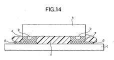
- a protruded terminal for connection (hereinafter called a bump) b is formed on the bottom electrode (not shown) of a semiconductor chip a and after the bump b and an electrode area d of a wiring pattern on a circuit board c are positioned, both are connected via joining material e such as solder and conductive paste.
- a problem is pointed out such that the manufacturing cost is increased because (1) a process for supplying and hardening the joining material e for connecting the bump b and the electrode area d of the wiring pattern is complex, (2) an insulating resin f called underfill is filled between the chip a and the board c so as to seal a bump connection portion between the bump b and the electrode area d and thereby to acquire the reliability in the moisture-proof of the bump connected part and strength for mounting the semiconductor chip and (3) a process for filling and hardening the insulating resin f to be underfill is required.
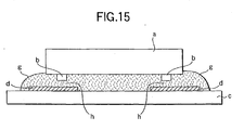
- FIG. 15 Another example of the flip-chip connection method (a second related art type method) is shown in Fig. 15.
- the second related art type method is proposed to solve the problem of the first related art type method and a bare semiconductor chip is mounted on a circuit board using an anisotropic conductive sheet proposed in Japanese Patent No. 2586154 .
- an anisotropic conductive sheet g in which conductive particulates are dispersed in thermoplastic or thermosetting resin is put between a bare semiconductor chip a and a circuit board c, and the resin is made to flow by thermocompression bonding, so that electric connection in the direction of the thickness is acquired by conductive particulates h put between a bump b and an electrode area d of the wiring pattern.
- the anisotropic conductive sheet g is relatively high-priced
- the anisotropic conductive sheet cannot be used for a board without heat resistance because the high temperature of 200°C or more is required for hardening the sheet
- it takes 10 to 20 seconds to harden the resin though it is a relatively short time and it is difficult to further simplify and speed up the process
- the reliability of connection is low because electric connection between the bump and the wiring pattern depends upon the contact of conductive particulates dispersed in the resin.
- the invention is made to solve the problems in the related art type flip-chip connection method and the object is to provide a method of mounting semiconductor chip by a flip-chip connection method in which a semiconductor chip can be mounted on a circuit board promptly, electrically and mechanically securely and further at a low cost.
- Another object of the invention is to provide a circuit board for flip-chip connection suitable for the above-mentioned mounting method.
- further another obj ect of the invention is to provide a method of manufacturing a circuit board for flip-chip connection in which the above-mentioned circuit board can be manufactured simply and at a low cost.
- furthermore another object of the invention is to provide an electromagnetic wave readable data carrier and a method of manufacturing the same in which an electromagnetic wave readable data carrier that functions as a flight tag, a label for physical distribution management, a ticket for an unmanned wicket and others can be produced at a low cost in a mass.
- further another object of the invention is to provide an electronic component module for an electromagnetic wave readable data carrier.
- a method of mounting a semiconductor chip according to the invention is provided with a process for pushing a melted thermoplastic resin coat aside by pressing a bump of a bare semiconductor chip on the melted thermoplastic resin coat applying an ultrasonic wave in a state in which the thermoplastic resin coat covering an electrode area on a wiring pattern is heated and melted and touching the bump and the electrode area, a process for bonding the bump and the electrode area by continuously applying an ultrasonic wave in a state in which the bump and the electrode area are touched and a process for cooling and solidifying the melted thermoplastic resin and bonding the body of the bare semiconductor chip on a circuit board.
- thermoplastic resin coat covering an electrode area on a wiring pattern is heated and melted
- a thermoplastic resin coat is formed beforehand in an electrode area on a wiring pattern of a circuit board used in the invention.
- This coat may also cover only an electrode area of a wiring pattern and may also cover the overall surface of a wiring pattern.
- an electrode area on a wiring pattern described above means a fixed small area on a wiring pattern including a position for a terminal of an electronic component and others to be connected. In this electrode area, a part generally called a land and others on the wiring pattern is included.
- thermoplastic resin described above has a satisfactory characteristic as an adhesive.
- action and effect are acquired that (1) secure electric conduction is acquired because the junction of the bump and the electrode area is diffused junction by an ultrasonic wave, (2) moisture-proof is satisfactory because the junction is sealed with resin, (3) mechanical mounting strength to pulling and others is high because the semiconductor chip and the circuit board are bonded when the thermoplastic resin is hardened, (4) electric conduction and mechanical bonding are simultaneously enabled in a short time, (5) the manufacturing cost is low because a process for special sealing and bonding and bonding material are not required and (6) the surface of the board is nevermore sticky than required in heating because no thermoplastic resin coat exists in a part in which the surface of the board is exposed.
- the overall surface of the wiring pattern of the circuit board for flip-chip connection according to the invention is covered with a thermoplastic resin coat.
- thermoplastic resin coat in case the circuit board described above is used for the mounting method described above, sealed structure satisfactory in moisture-proof and bonded structure high in tensile strength are acquired.
- thermoplastic resin is used for an etching mask used when the wiring pattern is formed by etching processing.
- thermoplastic resin coat covering the overall surface of a conductive pattern as it is, a special coat formation process is not required and much labor is not required, and therefore the manufacture at a low cost can be realized.
- the body of a data carrier in which a curled conductive pattern composing an antenna coil is held on thin or sheet insulating base material and an electronic component module in which a bare semiconductor chip composing a send and receive circuit, a memory and others is mounted on a wiring pattern of a thin or sheet circuit board are integrated.
- a process for manufacturing the electronic component module in which the bare semiconductor chip is mounted on the wiring pattern of the thin or sheet circuit board is mainly characteristic.
- a subprocess for pushing a melted thermoplastic resin coat aside by pressing a bump of the bare semiconductor chip on the melted thermoplastic resin coat applying an ultrasonic wave in a state in which the thermoplastic resin coat covering the electrode area on the wiring pattern is heated and melted and touching the bump and an electrode area a subprocess for bonding the bump and the electrode area by continuously applying an ultrasonic wave in a state in which the bump and the electrode area are touched and a subprocess for cooling and solidifying the melted thermoplastic resin and bonding the body of the bare semiconductor chip on the circuit board are included.
- the electromagnetic wave readable data carrier that functions as a flight tag, a label for physical distribution management, a ticket for an unmanned wicket and others can be produced at a low cost in a mass owing to action and effect that (1) secure electric conduction is acquired because the junction of the bump and the electrode area is diffused junction by an ultrasonic wave, (2) moisture-proof is satisfactory because the junction is sealed with resin, (3) mechanical mounting strength to pulling and others is high because the semiconductor chip and the circuit board are bonded when the thermoplastic resin is hardened, (4) electric conduction and mechanical bonding are simultaneously enabled in a short time, (5) the manufacturing cost is low because a process for special sealing and bonding and bonding material are not required and (6) the surface of the board is never more sticky than required in heating because no thermoplastic resin coat exists in a part in which the surface of the board is exposed.
- thermoplastic resin coat the overall surface of a wiring pattern of a circuit board used in the manufacturing process of the electronic component module according to the invention is covered with a thermoplastic resin coat.
- thermoplastic resin coat As the overall surface of the wiring pattern is covered with the thermoplastic resin coat in case the above-mentioned circuit board is used in the electronic component module manufacturing process, sealed structure satisfactory in moisture-proof and bonded structure high in tensile strength are acquired.
- thermoplastic resin is used as an etching mask used when a wiring pattern is formed by etching processing.
- the etching mask used in the etching processing for forming the wiring pattern becomes a thermoplastic resin coat covering the overall surface of a conductive pattern as it is, a special coat formation process is not required and much labor is not required, and therefore the manufacture at a low costcan be realized.
- the body of a data carrier in which a metallic foil pattern composing an antenna coil is heldon thin resin base material, and an electronic component module in which a bare semiconductor chip composing a send and receive circuit, a memory and others is mounted on a aluminum foil wiring pattern on the surface of thin resin base material are integrated.
- the electromagnetic wave readable data carrier manufacturing method a process for manufacturing the electronic component module in which the bare semiconductor chip is mounted on the aluminum foil wiring pattern on the surface of the thin resin base material is mainly characteristic.
- the overall surface of the aluminum foil wiring pattern of the circuit board according to the invention is covered with a thermoplastic resin coat.
- thermoplastic resin is used as an etching mask used when the aluminum foil wiring pattern is formed by etching processing.
- thermoplastic rein polyolefin resin or polyester resin is used.
- Action and effect can be desired by using such resin such that the resistance to a chemical satisfactory for an etching mask, and satisfactory junction strength between a metallic bump on the side of the semiconductor chip and a metallic electrode area on the side of the wiring pattern are acquired. That is, polyolefin resin is provided with satisfactory resistance to alkaline etchant such as NaOH or polyester resin is provided with satisfactory resistance to acid etchant such as FeCl 2 . In addition, these resins are also excellent in an adhesive property.
- an electronic component module for an electromagnetic wave readable data carrier comprises: a circuit board having a wiring pattern with an electrode area and a thermoplastic resin coat covering the electrode area of the wiring pattern; and a semiconductor chip mounted on the circuit board, said semiconductor chip having a bump at a side of the circuit board thereof.
- the bump of the semiconductor chip penetrates the thermoplastic resin coat and directly bonds with the electrode area of the wiring pattern.
- an electromagnetic wave readable data carrier comprises: a body of a data carrier including an insulating base material and a conductive pattern held on the insulating base material; and an electronic component module including a circuit board and a semiconductor chip mounted on the circuit board, said circuit board having a wiring pattern with an electrode area and a thermoplastic resin coat covering the electrode area of the wiring pattern, said semiconductor chip having a bump at a side of the circuit board thereof, the bump of the semiconductor chip penetrating the thermoplastic resin coat and directly bonding with the electrode area of the wiring pattern, wherein said electronic component module is manufactured by a method comprising: heating and melting the thermoplastic resin coat of said circuit board; pressing the bump of said semiconductor chip on the thus melted thermoplastic resin coat while applying an ultrasonic wave to the bump so that the bump penetrates the melted thermoplastic resin coat and brings into contact with electrode area; bonding the bump and the electrode area by continuously applying the ultrasonic wave to the bump bringing into contacted with the electrode area; and cooling and solidifying the melted thermo
- the semiconductor chip mounting method is provided with: 1) a process for pushing a heated and melted thermoplastic resin coat covering an electrode area on a wiring pattern aside by pressing a bump of a bare semiconductor chip on the melted thermoplastic resin coat applying an ultrasonic wave so as to bring the bump into contact with the electrode area; 2) a process for bonding the bump and the electrode area by continuously applying an ultrasonic wave in a state in which the bump and the electrode area are in contact; and 3) a process for cooling and solidifying the melted thermoplastic resin and bonding the body of the bare semiconductor chip on a circuit board.
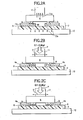
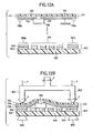
- FIG. 1A-E An outline of a series of processes including such a mounting method is shown in a process drawing shown in Figs. 1A-E.
- a metallic foil lamination manufacturing process A
- an etching mask printing process B
- an etching process for forming a wiring pattern C
- an ultrasonic mounting process D
- a bonding process E
- an Al-PET lamination 1 which is original material of a thin circuit board is manufactured.
- the Al-PET lamination 1 is manufactured in a process for laminating hard aluminum foil 3 having the thickness of 35 ⁇ m on the single side (the upper surface in Fig. 1A) of a PET film 2 having the thickness of 25 ⁇ m via an urethane adhesive, and bonding them thermally under a condition of the temperature of 150°C and the pressure of 5 kg/cm 2 .
- an etching resist pattern 4 in the shape of a required wiring pattern is formed on the surface of the hard aluminum foil 3 of the Al-PET lamination 1.
- the resist pattern 4 is formed by applying a polyolefin thermoplastic resin adhesive, which is melted at the temperature of approximately 150°C, on the surface of the hard aluminum foil 3 by approximately 4 to 6 ⁇ m in thickness by a method such as gravure. It is desirable that this thickness is varied according to the size and the shape of a bump of a mounted bare chip.
- a wiring pattern 6 composed of the hard aluminum foil 3 is formed by removing an aluminum foil part 5 exposed from the etching resist pattern 4 by well-known etching process.
- the wiring pattern 6 is formed by exposing the aluminum foil part 5 exposed from the etching resist pattern 4 to NaOH (120 g/l) used as etchant under a condition of the temperature of 50°C.
- the wiring pattern 6 composed of the hard aluminum foil 3 appears on the surface of a circuit board 7 acquired in this etching process.
- the overall surface of the wiring pattern 6 is covered with the polyolefin thermoplastic resin adhesive used for the etching resist pattern (an etching mask) 4.
- the surface of at least an electrode area (an area to be connected with a bump of a bare semiconductor chip described later) of the wiring pattern 6 is covered with a thermoplastic resin coat 4a.
- a bare semiconductor chip 8 is mounted on the circuit board 7 applying an ultrasonic wave.
- This process includes: 1) a subprocess (a first subprocess) for pushing the melted thermoplastic resin coat 4a aside by pressing a bump 9 of the bare semiconductor chip 8 on the melted thermoplastic resin coat 4a in a state in which the thermoplastic resin coat 4a covering an electrode area 10 on the wiring pattern 6 is heated and melted applying an ultrasonic wave so as to bring the bump 9 into contact with the electrode area 10 ; and 2) a subprocess (a second subprocess) for bonding the bump 9 and the electrode area 10 in a state in which the bump 9 and the electrode area 10 are contacted with each other by continuously applying an ultrasonic wave.
- the bare semiconductor chip 8 is composed as a so-called surface mounting-type component. That is, the bare semiconductor chip 8 has a body which has 150 ⁇ m thick and the bump 9 which is a metallic terminal for connection and protruded from the bottom of the bare semiconductor chip 8..
- the bump (made of gold for example) 9 is pressed on the thermoplastic resin coat 4a which is melted by heating at 150°C in a state in which an ultrasonic wave is applied. Then, the melted thermoplastic resin coat 4a is pushed aside and removed from the position of the end of the bump 9 by the ultrasonic vibration of the bump 9. Further, an oxide layer and others on the surface of the aluminum foil wiring pattern 6 are also mechanically removed by the vibration.
- the bump 9 and the electrode area 10 are contacted with each other.
- the bump 9 and the electrode area 10 of the wiring pattern 6 are further heated by frictional heat by the vibration, a metallic fused part in which atoms of gold are diffused in the aluminum foil is formed and the bonding of both by an ultrasonic wave is completed.
- the first and second subprocesses are completedby applying ultrasonic vibration of the frequency of 63 kHz by approximately a few seconds under the pressure of 0.2 kg/mm 2 for example after the bare semiconductor chip 8 is arranged in a predetermined position.
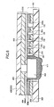
- a process drawing shown in Figs. 2A-C The details of the ultrasonic mounting process are shown in a process drawing shown in Figs. 2A-C.
- a positioning process shown in Fig. 2A in a state in which an ultrasonic horn 11 and an anvil 12 used as a heater table respectively provided with a vacuum attraction function are arranged opposite, the bare chip 8 is attracted to the ultrasonic horn 11 as shown by an arrow 11a and the circuit board 7 is attracted to the anvil 12 as shown by an arrow 12a.
- the bump 9 on the side of the bare chip 8 and the electrode area 10 of the wiring pattern 6 on the side of the circuit board 7 are positioned, relatively moving the ultrasonic horn 11 and the anvil 12 in a horizontal direction.
- the circuit board 7 is heated up to 150°C by the anvil 12.
- thermoplastic resin adhesive shown in Fig. 2B
- the melted thermoplastic resin coat 4a is pushed aside by pressing the bump 9 of the bare chip 8 on the thermoplastic resin adhesive (the thermoplastic resin coat) 4a in a heated and melted state by applying pressure (0.1 to 0.3 kgf) as shown by an arrow P, as applying ultrasonic vibration (63.5 kHz, 2W) as shown by an arrow v by the ultrasonic horn 11 and the anvil 12. Therefore, the bump 9 and the electrode area 10 are contacted with each other.
- thermoplastic resin coat 4a is hardened again by natural cooling or forced cooling by removing the heat of 150°C applied to the circuit board. Therefore, the bare semiconductor chip 8 and the wiring pattern 6 are bonded. That is, the thermoplastic resin coat 4a in a melted state filled between the bottom of the bare semiconductor chip 8 and the circuit board 7 is cooled and solidified, and the bare semiconductor chip 8 and the circuit board 7 are firmly bonded and fixed.
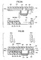
- the mounted structure completed in the processes (A) to (E) is shown in Fig. 3.
- action and effect are acquired such that (1) sure electric conduction is acquired because the bump 9 and the electrode area 10 are bonded by diffused junction by an ultrasonic wave, (2) the moisture-proof is satisfactory because a junction between the bump 9 and the electrode area 10 is sealed with resin, (3) the mechanical strength of mounting for pulling and others is high because the semiconductor chip 8 and the circuit board 7 are bonded when the thermoplastic resin coat 4a is hardened, (4) electric conduction and mechanical coupling are simultaneously enabled in a short time, (5) the manufacturing cost is particularly low because special processes from sealing to bonding and adhesive material are not required and (6) the surface of the board is never more sticky than required in heating because no thermoplastic resin coat exists in a part in which the surface of the board is exposed.
- the strength of bonding between the bare semiconductor chip 8 and the wiring pattern 6 in the case of the mounting method using the resin coat in this embodiment is shown in Fig. 4 in comparison with a case using only ultrasonic bonding.
- Fig. 4 in the case of the mounting method according to the invention, the double to triple strength of bonding is acquired, compared with the case of only ultrasonic bonding. It need scarcely be said that this is because the semiconductor chip 8 and the circuit board 7 are bonded when the thermoplastic resin coat 4a is hardened.
- the PET film 2 is used for resin base material composing the lamination 1, however, a polyimide film and others can be also used in place of the PET film.
- polyester thermoplastic resin can be also used in place of the polyolefin resin.
- FeCl 2 is used for etchant.
- the overall surface of the wiring pattern 6 is covered with the thermoplastic resin coat 4a and the circuit board can be generalized as a circuit board for flip-chip connection.
- thermoplastic resin coat 4a located in the vicinity of the electrode area 10 on the wiring pattern 6 mainly contributes to sealing the ultrasonic junction, while the thermoplastic resin coat 4a located in a part except the electrode area contributes to the bonding of the body of the semiconductor chip 8 and the circuit board 7.
- thermoplastic resin is used for an etching mask used when the wiring pattern is formed by etching processing and the circuit board manufacturing method can be generalized as a method of manufacturing a circuit board for flip-chip connection.
- the material of the etching mask used in etching processing for forming the wiring pattern becomes the thermoplastic resin coat covering the overall surface of a conductive pattern as it is, a coat formation process is not required and labor is not required. Therefore the manufacture at a low cost is realized.
- This data carrier functions as a flight tag, a label for physical distribution management, a ticket for an unmanned wicket and others and can read an electromagnetic wave.
- This data carrier is composed by integrating the body of the data carrier with an electronic component.
- a metallic foil pattern composing an antenna coil is held on thin resin base material.
- a bare semiconductor chip composing a send and receive circuit, a memory and others is mounted on an aluminum foil wiring pattern on the surface of the thin resin base material.
- the data carrier DC is provided with the body of the data carrier 100 and an electronic component module 200.
- a copper foil curled conductive pattern (equivalent to an antenna coil) 102 having the thickness of 10 ⁇ m is held on the single side of polyethylene terephthalate (PET) base material 101 having the thickness of 25 ⁇ m.
- PET polyethylene terephthalate
- bare chip IC 202 is mounted on the lower side in Fig. 5 of a glass epoxy piece 201 having the thickness of 70 ⁇ m.
- the electronic component module 200 is mounted on the body of the data carrier 100 so that the piece 201 crosses an orbital conductive flux 102a composing the curled conductive pattern 102. Electric connection of the electronic component module 200 with the curled conductive pattern 102 is performed in a terminal pad on the inner side 103 and in a terminal pad on the outer side 104 of the curled conductive pattern 102.
- FIG. 6 An example of the structure in which the electronic component module 200 is mounted is shown in an enlarged sectional view in Fig. 6.
- a method of manufacturing the body of the data carrier 100 and the electronic component module 200 respectively shown in Figs. 5 and 6 will be sequentially described in detail below.
- FIGs. 7A-E An example of the manufacturing process of the curled conductive pattern 102 composing an antenna coil is shown in Figs. 7A-E. Referring to Figs. 7A-E, a process when the curled conductive pattern 102 to be an antenna coil is formed on the single side of the PET film base material 101 will be described.
- a Cu-PET lamination 301 is prepared.
- copper foil 303 having the thickness of 10 ⁇ m is laminated on the single side of a PET film 302 having the thickness of 25 ⁇ m via an urethane adhesive. Then they is thermically bonded under a condition of the temperature of 150°C and the pressure of 5 kg/cm 2 .
- the Cu-PET lamination 301 in which the cupper foil 303 is bonded on the surface of the PET film 302 is completed.
- a curled etching resist pattern 304 is formed on the surface of the copper foil 303 of the Cu-PET lamination 301. That is, insulating etching resist ink is printed on the copper foil 303 using an offset printing method for example so that the insulating etching resist ink has a curled shape having the number of turns, the width, the pitch and the inside and outside circumferences for acquiring an L value and a Q value respectively required for the characteristics of a coil.
- a type hardened by heat or an active energy beam is used.
- the active energy beam ultraviolet rays or an electron beam is used. In case ultraviolet rays are used, the resist ink including a photopolymerization agent and is used.
- conductive etching resist patterns 305a and 305b (103 and 104 in Fig. 5) in the shape of a required electrode are formed by conductive ink in a position for electric connection with the electrode of the electronic component module 200 on the surface of the copper foil 303 of the Cu-PET lamination 301.
- These resist patterns 305a and 305b are formed by offset printing as in the above-mentioned process.
- resist ink a thermosetting conductive adhesive hardened by heat treatment at 120°C for approximately 20 minutes is used.
- a screen printing method generally performed may be also used for the printing of conductive ink in this process.
- ink material a chemical acquired by adding a photopolymerization agent to the mixture of Ag particles and an thermoplastic adhesive for example or solder paste and others may be also used.
- a copper foil part 306 exposed from the etching resist patterns 304, 305a and 305b is removed by executing well-known etching and a curled conductive pattern (102 in Fig. 5) to be an antenna coil is formed.
- FeCl 2 120 g/l
- the copper foil 303 is removed.
- an electronic component cannot be mounted on a circuit, that is, on a curled pattern composing an antenna coil.
- the conductive resist patterns 305a and 305b are provided and etching resist is not required to be removed by mounting an electronic component in this position. That is, a process for peeling the etching resist can be omitted by the invention. Further, there is also effect that the etching resist 304 formed by insulating ink also functions as an insulating protective layer on the surface of the copper foil circuit pattern.
- a transparent hole 307 into which a convex portion(a potting part 411) described later of the electronic component module can be inserted is formed by a press process.
- FIGs. 8A-E an example of the manufacturing process of the electronic component module 200 is shown in Figs. 8A-E.
- the contents shown in Figs. 8A-E are the same as the contents described above referring to Figs. 1A-E except that a bare chip 408 is sealed with resin in the potting part 411 in a final process and conductive resist 412 is arranged in an electrode part for connection with the body of the data carrier 100.
- an Al-PET lamination 401 which is the base material of a thin circuit board is manufactured.
- the Al-PET lamination 401 is manufactured in a process for laminating hard aluminum foil 403 having the thickness of 35 ⁇ m on the single side (the upper surface in Fig. 8A) of a PET film 402 having the thickness of 25 ⁇ m via an urethane adhesive and thermically bonding them under a condition of the temperature of 150°C and the pressure of 5 kg/cm 2 .
- an etching resist pattern 404 in the shape of a required wiring pattern is formed on the surface of the hardaluminum foil 403 of theAl-PET lamination 401.
- the resist pattern 404 is formed by applying a polyolefin thermoplastic resin adhesive, which is melted at the temperature of approximately 150°C, on the surface of the hard aluminum foil 403 by approximately 4 to 6 ⁇ m in thickness by a method such as gravure. It is desirable that the applied thickness is adjusted according to the size and the shape of a bump of a mounted bare chip.
- conductive etching resist patterns 412a and 412b in the shape of a required electrode pattern are arranged in each connection with terminal pads 305a and 305b of the body of the data carrier 100.
- These resist patterns 412a and 412b are formed by offset printing as in the above-mentioned process.
- resist ink a thermosetting conductive adhesive hardened by heat treatment at 120°C for approximately 20 minutes is used.
- screen printing generally performed may be also used.
- ink material a chemical in which a photopolymerization agent is added to the mixture of Ag particles and an thermoplastic adhesive for example or solder paste and others may be also used.
- a wiring pattern 406 made of hard aluminum foil 403 is formed by removing an aluminum foil part 405 exposed from the etching resist pattern 404 by well-known etching processing.
- this wiring pattern 406 is formed by exposing the aluminum foil part 405 exposed from the etching resist pattern 404 to NaOH (120 g/l) which is etchant under a condition of the temperature of 50°C.
- the wiring pattern 406 made of hard aluminum foil 403 appears on the surface of a circuit board 407 acquired in this etching process.
- the overall surface of the wiring pattern 406 is covered with the polyolefin thermoplastic resin adhesive used for the etching resist pattern (an etching mask) 404.
- the surface of at least the electrode area (an area to be connected with the bump of the bare semiconductor chip described later) of this wiring pattern 406 is covered with a thermoplastic resin coat 404a.
- the bare semiconductor chip 408 is mounted on the circuit board 407 applying an ultrasonic wave.
- This process includes: 1) a first subprocess for pushing the melted thermoplastic resin coat 404a aside by pressing a bump 409 of the bare semiconductor chip 408 on the melted thermoplastic resin coat 404a applying an ultrasonic wave in a state in which the thermoplastic resin coat 404a covering an electrode area 410 on the wiring pattern 406 is heated and melted so as to bring the bump 409 into contact with the electrode area 410 and 2) a second subprocess for bonding the bump 409 and the electrode area 410 by continuously applying an ultrasonic wave in a state in which the bump 409 and the electrode area 410 are contacted with each other.
- the bare semiconductor chip 408 is composed as a so-called surface mounting-type component. That is, the bare semiconductor chip 408 has a body which is 150 ⁇ m thick and the bump 409 which is a metallic terminal for connection and protruded form the bottom of the bare semiconductor 408.
- the bump (made of gold for example) 409 is pressed on the thermoplastic resin coat 404a which is melted by heating at 150°C applying ultrasonic vibration. Then, the melted thermoplastic resin coat 404a is pushed aside and removed from the end position of the bump 409 by the ultrasonic vibration of the bump 409. Further, an oxide layer and others on the surface of the aluminum foil wiring pattern 406 are also mechanically removed by the vibration.
- the bump 409 and the electrode area 410 are contacted with each other.
- the bump 409 and the electrode area 410 of the wiring pattern 406 are heated by frictional heat by the vibration further, a metallic fused part in which atoms of gold are diffused in the aluminum foil is formed and the ultrasonic junction of both is completed.
- the first and second subprocesses are completedby applying ultrasonic vibration at the frequency of 63 kHz for approximately a few seconds under the pressure of 0.2 kg/mm 2 for example after the bare semiconductor chip 408 is arranged in a predetermined position.
- the melted thermoplastic resin coat 404a is rehardened by natural cooling or forced cooling by removing the heat of 150°C applied to the circuit board, and the body of the bare semiconductor chip 408 and the wiring pattern 406 are bonded. That is, the melted thermoplastic resin coat 404a filled between the bottom of the bare semiconductor chip 408 and the circuit board 407 is cooled and solidified, and the bare semiconductor chip 408 and the circuitboard 407 are firmly bonded and fixed. Afterward, the bare semiconductor chip 408 is sealed with resin by a well-known method if necessary and the potting part 411 is formed.
- the electronic component module 200 is mounted on the body of the data carrier 100 so that the electronic component mounted side of the electronic component module 200 and the conductive pattern formation side of the body of the data carrier 100 are opposite, and the electronic component module 200 crosses the orbital conductive flux 102a composing the curled conductive pattern 102.
- the potting part 411 covering the bare chip 408 which is an electronic component is inserted into the hole 307 made on the side of the body of the data carrier 100.
- the conductive resist areas 412a and 412b to be electrode areas of a pair of aluminum foil areas 406 connected to the bumps 409 of the bare chip 408 on the side of the electronic component module 200 are respectively located over a pair of conductive resist patterns 305a and 305b on the side of the body of the data carrier 100. That is, the copper foil areas 406 on the side of the electronic component module 200 and the conductive resist patterns 305a and 305b on the side of the body of the data carrier 100 are respectively opposite via the conductive resist areas 412.
- indentators 501a and 501b heated up to 160°C are pressed particularly on a pair of conductive resist patterns 305a and 305b at the pressure of 21.7 kg for 20 seconds from over the electronic component module 200.
- the conductive resist pattern which is a thermoplastic adhesive coat is locally softened and melted, and the conductive resist areas 412a and 412b that respectively conduct to the terminal areas 406 of the electronic component module 200 and the conductive resist patterns 305a and 305b on the side of the body of the data carrier 100 are respectively bonded and fixed.
- the thermoplastic resin coat 404a can be utilized for the junction of the electronic component module 200 and the body of the data carrier 100 with the thermoplastic resin coat keeping insulation.
- the etching resist 304 on the surface of the curled conductive pattern 102 is left as insulating material. Therefore, a wiring pattern (not shown) on the insulating base material piece 402 (201) of the electronic component module 200 also functions as a jumper member mating the inside and the outside of the curled conductive pattern 102. As a result, the curled conductive pattern 102 and the bare chip 408 can be electrically connected without using a jumper member, a back wiring pattern and others as in related art type structure.
- This data carrier also functions as a flight tag, a label for physical distribution management, a ticket for an unmanned wicket and others and can also read an electromagnetic wave.
- This data carrier is also composed by integrating the body of a data carrier with electronic component module on the surface of the thin resin base material as in the embodiment described referring to Fig. 5.
- a metallic foil pattern composing an antenna coil is held on thin resin base material.
- a bare semiconductor chip composing a send and receive circuit, a memory and others is mounted on an aluminum foil wiring pattern.
- FIG. 10A-C An example of the manufacturing process of the curled conductive pattern 102 shown in Fig. 5 composing an antenna coil is shown in Figs. 10A-C.
- Figs. 10A-C processes when the curled conductive pattern 102 shown in Fig. 5 to be an antenna coil is formed on the single side of the PET film base material 101 as shown in Fig. 5 will be described below.
- Cu-PET lamination base material 601 is prepared.
- copper foil having the thickness of 10 ⁇ m is laminated on the single side of a PET film having the thickness of 25 ⁇ m via an urethane adhesive and is thermically bonded under a condition of the temperature of 150°C and the pressure of 5 kg/cm 2 .
- the Cu-PET lamination 601 in which the cupper foil 603 is bonded on the surface of the PET film 602 (101) is completed.
- a curled etching resist pattern 604 and an etching resist pattern 604 in the shape of a terminal are formed on the surface of the copper foil 603 of the Cu-PET lamination 601. That is, insulating etching resist ink is printed on the copper foil using an offset printing method for example so that the insulating etching resist ink has a curled shape having the number of turns, the width, the pitch and the inside and outside circumferences for acquiring an L value and a Q value respectively required for the characteristics of a coil.
- a type hardened by heat or an active energy beam is used.
- the active energy beam ultraviolet rays or an electron beam is used and in case ultraviolet rays are used.
- the resist ink including a photopolymerization agent is used.
- a curled conductive pattern 605 and terminal pads 606a and 606b on the inside and outside circumferences respectively composing an antenna coil are formed by removing a copper foil part 603a exposed from the etching resist pattern 604 formed in the above-mentioned process by well-known etching.
- FeCl 2 120 g/l is used for etchant under a condition of the temperature of 50°C and the required copper foil (Cu) is removed.
- the insulating etching resist 604 formed in the process B is removed, an electronic component cannot be mounted on a circuit, that is, on a coil.
- the insulating resist 604 is not required to be removed. That is, according to the invention, a process for peeling the etching resist 604 canbeomitted. Further, effect is acquired such that the etching resist 604 can be used for an insulating protective layer on the surface of the copper conductive pattern 605.
- anAl-PET lamination 701 which is original material of a thin circuit board is manufactured.
- the Al-PET lamination 701 is manufactured in a process for laminating hard aluminum foil 703 having the thickness of 35 ⁇ m on the single side (the upper surface in Figs. 11 A-E) of a PET film 702 having the thickness of 25 ⁇ m via an urethane adhesive and bonding them thermally under a condition of the temperature of 150°C and the pressure of 5 kg/cm 2 .
- an etching resist pattern 704 in the shape of a required wiring pattern is formed on the surface of the hard aluminum foil 703 of theAl-PET lamination 701.
- the resist pattern 704 is formed by applying a polyolefin thermoplastic resin adhesive, which is melted at the temperature of approximately 150°C, on the surface of the hard aluminum foil 703 by approximately 4 to 6 ⁇ m in thickness by a method such as gravure. It is desirable that this thickness is varied according to the size and the shape of a bump of a mounted bare chip.
- a wiring pattern 706 made of the hard aluminum foil 703 is formed by removing an aluminum foil part 705 exposed from the etching resist pattern 704 by well-known etching processing.
- the wiring pattern 706 is formed by exposing the aluminum foil part 705 exposed from the etching resist pattern 704 to NaOH (120 g/l) which is etchant under a condition of the temperature of 50°C.
- the wiring pattern 706 made of the hard aluminum foil 703 is formed on the surface of a circuit board 707 acquired in this etching process.
- the overall surface of the wiring pattern 706 is covered with the polyolefin thermoplastic resin adhesive used for the etching resist pattern (an etching mask) 704.
- the surface of at least an electrode area (an area to be connected with a bump of a bare semiconductor chip described later) of the wiring pattern 706 is covered with a thermoplastic resin coat 704a.
- a bare semiconductor chip 708 is mounted on the circuit board 707 applying an ultrasonic wave.
- This process includes: 1) a subprocess (a first subprocess) for pushing the melted thermoplastic resin coat 704a aside by pressing a bump 709 of the bare semiconductor chip 708 on the melted thermoplastic resin coat 704a in a state in which the thermoplastic resin coat 704a covering an electrode area 710 on the wiring pattern 706 is heated and melted applying an ultrasonic wave so as to bring the bump 709 into contact with the electrode area 710; and 2) a subprocess (a second subprocess) for bonding the bump 709 and the electrode area 710 in a state in which the bump 709 and the electrode area 710 are contacted with each other by continuously applying an ultrasonic wave.
- the bare semiconductor chip 708 is composed as a so-called surface mounting-type component. That is, the bare semiconductor chip 708 has a body which is 150 ⁇ m thick and the bump 709 which is a metallic terminal for connection and protruded form the bottom of the bare semiconductor chip 708.
- the bump (made of gold for example) 709 is pressed on the thermoplastic resin coat 704a which is melted by heating at 150°C applying an ultrasonic wave. Then, the melted thermoplastic resin coat 704a is pushed aside and removed from the position of the end of the bump 709 by the ultrasonic vibration of the bump 709. Further, an oxide layer and others on the surface of the aluminum foil wiring pattern 706 are also mechanically removed by the vibration.
- the bump 709 and the electrode area 710 are contacted with each other.
- the bump 709 and the electrode area 710 of the wiring pattern 706 are further heated by frictional heat by the vibration, a metallic fused part in which atoms of gold are diffused in the aluminum foil is formed and the bonding of both by an ultrasonic wave is completed.
- the first and second subprocesses are completedby applying ultrasonic vibration of the frequency of 63 kHz by approximately a few seconds under the pressure of 0.2 kg/mm 2 for example after the bare semiconductor chip 708 is arranged in a predetermined position.
- the melted thermoplastic resin coat 704a is hardened again by natural cooling or forced cooling by removing the heat of 150°C applied to the circuit board, and the body of the bare semiconductor chip 708 and the wiring pattern 706 are bonded. That is, the thermoplastic resin coat 704a in a melted state filled between the bottom of the bare semiconductor chip 708 and the circuit board 707 is cooled and solidified, and the bare semiconductor chip 708 and the circuit board 707 are firmly bonded and fixed. Afterward, the bare semiconductor chip 708 is sealed with resin by a well-known method if necessary and a potting part 711 is formed. As a result, an electronic component module 707 is completed.
- a process for mounting the electronic component module 707 on the data carrier 607 and electrically connecting with an antenna coil will be described. This process is executed using ultrasonic welding technology.
- the electronic component module 707 is mounted on the body of the data carrier 607 in a matched state that parts to be bonded 708a and 708b on the side of the electronic component and terminal pads 606a and 606b which are parts to be bonded on the side of the body of the data carrier are opposite.
- indentators 801 and 802 that fall integrally are pressed over the parts to be bonded 708a and 708b of the electronic component module 707 by time T (approximately 0.5 second) applying the ultrasonic vibration of applied pressure P (0.2 kg/mm 2 ) and a frequency V (40 kHz).
- Reference numbers 803 and 804 denote anvils arranged opposite to the indentators 801 and 802.
- welding is caused by bringing atoms at distance (a few angstrom ( ⁇ )) at which attraction is exerted between atoms on the surfaces of metals to be bonded and contacting with the surfaces with atoms on the overall surfaces orderly arrayed.
- ⁇ angstrom
- the approach of clean metallic atoms under it is prevented and sufficient bonding power is not caused.
- the terminal of the electronic component module and the terminal on the side of the antenna coil are bonded and fixed by removing a metallic superficial layer by ultrasonic vibration by the above-mentioned method, further activating the vibration of atoms and diffusing atoms.
- this method is based upon a principle that bonding is realized by removing a metallic superficial layer by ultrasonic vibration as described above and even if the bonding process is executed in a state in which insulating etching resist 704 formed on the terminal pads 606a and 606b of the conductive pattern is not peeled as shown in the process (B) in Fig. 12B, a sufficient electric and mechanical bonding characteristic is acquired between the side of the electronic component module 707 and the side of the body of the data carrier 607.
- the thin data carrier DC (see Fig. 5) according to the invention is completed by the processes described above.
- the plastic flow of metal is locally caused corresponding to the protruded part by providing multiple irregularities corresponding to the shape of the fused part to the end face of the anvils 803 and 804 opposite to the indentators 801 and 802 for example and in the meantime, adjusting the pressing time of the indentators 801 and 802 and resin layers exposed from a part from which a metallic layer is removed can be fused by ultrasonic vibration.
- the mechanical bonding strength of the electronic component module is particularly enhanced in case such fusion of metal and the fusion of resin are both used, the data carrier is effective when it is often roughly handled as a flight tag and a label for physical distribution management.
- the thin data carrier completed as described above uses an electromagnetic field as a read medium, it can securely read data stored in the semiconductor chip apart by the distance of 100 to 1000 mm without being restricted by distance and a direction in reading so much, concretely without being restricted by the direction of reading.
- the result of the moisture-proof test (at the temperature of 85°C and at the humidity of 85%) of the thin data carrier manufactured in this embodiment is shown in Fig. 13.
- the variation of communication distance after 250 hours elapse in the moisture-proof test is within ⁇ 10%. It is verified that for reliability on the moisture-proof of the connection of the bump, a sufficient value is acquired.
- the semiconductor chip mounting method by the flip-chip connection method in which the semiconductor chip can be mounted on the circuit board promptly, electrically and mechanically securely and further, at a low cost can be provided.
- the electromagnetic wave readable data carrier manufacturing method in which the electromagnetic wave readable data carrier that functions as a flight tag, a label for physical distribution management, a ticket for an unmanned wicket and others can be produced at a low cost in a mass can be provided.
Abstract
Description
- The present invention relates to a method of mounting a semiconductor chip which is suitable for manufacturing an electromagnetic wave readable data carrier that functions as a flight tag, a label for physical distribution management, a ticket for an unmanned wicket and others, particularly relates to a method of mounting semiconductor chip in which a bare semiconductor chip can be mounted on a circuit board at a low cost by a flip-chip connecting method. The present invention also relates to a circuit board for flip-chip connection and a method of manufacturing the same. In addition, the present invention relates to an electromagnetic wave readable data carrier and a method of manufacturing the same, and an electronic component module for an electromagnetic wave readable data carrier.
- For this type of electromagnetic wave readable data carrier, a flight tag disclosed in
Japanese Patent Unexamined Publication No. Hei. 6-243358 - The flight tag disclosed in the patent application is composed by mounting a curled conductive pattern to be an antenna coil and IC components to be a send and receive circuit, a memory and others on the single side of a rectangular substrate made of a PET film.
- The body of the flight tag that holds the curled conductive pattern to be an antenna coil can be formed by selectively etching copper foil and aluminum foil respectively coated on the single side of the PET film by etching processing. Therefore, a continuous production line by roll to roll (RTR) can be readily realized by a resist formation process by well-known photolithographic technology and the succeeding wet etching process and others. In the meantime, circuit components such as a send and receive circuit and a memory to be mounted on the body of the flight tag are integrated in one chip using semiconductor integration technology.
- These applicants propose that a bare semiconductor chip is first moduled by mounting the bare semiconductor chip composing the send and receive circuit, the memory respectively described above and others on a thin insulating piece (a type of circuit board) and then the productivity of a flight tag is enhanced by bonding the electronic component module on a PET film composing the body of the flight tag.
- As for an electronic component mounted sheet, the advanced thinning of which is requested, such as the electronic component module bonded to the flight tag, a flip-chip connection method in which a bare semiconductor chip is directly mounted on a circuit board is often proposed.
- An example of the flip-chip connection method (hereinafter called a first related art type method) is shown in Fig. 14. In the first related art type method, a protruded terminal for connection (hereinafter called a bump) b is formed on the bottom electrode (not shown) of a semiconductor chip a and after the bump b and an electrode area d of a wiring pattern on a circuit board c are positioned, both are connected via joining material e such as solder and conductive paste.
- In the first related art type method, a problem is pointed out such that the manufacturing cost is increased because (1) a process for supplying and hardening the joining material e for connecting the bump b and the electrode area d of the wiring pattern is complex, (2) an insulating resin f called underfill is filled between the chip a and the board c so as to seal a bump connection portion between the bump b and the electrode area d and thereby to acquire the reliability in the moisture-proof of the bump connected part and strength for mounting the semiconductor chip and (3) a process for filling and hardening the insulating resin f to be underfill is required.
- Another example of the flip-chip connection method (a second related art type method) is shown in Fig. 15. The second related art type method is proposed to solve the problem of the first related art type method and a bare semiconductor chip is mounted on a circuit board using an anisotropic conductive sheet proposed in
Japanese Patent No. 2586154 - In the second related art type method, an anisotropic conductive sheet g in which conductive particulates are dispersed in thermoplastic or thermosetting resin is put between a bare semiconductor chip a and a circuit board c, and the resin is made to flow by thermocompression bonding, so that electric connection in the direction of the thickness is acquired by conductive particulates h put between a bump b and an electrode area d of the wiring pattern.
- According to this method, there is effect that the positioning of the circuit board with the wiring pattern when the semiconductor chip is mounted on the circuit board can be relatively roughly performed. In addition, time when resin is hardened is short, for example 10 to 20 seconds, sealing material such as underfill is not required tobe used, and the manufacturing cost can be reduced. To the contrary, problems are further pointed out such that (1) the anisotropic conductive sheet g is relatively high-priced, (2) the anisotropic conductive sheet cannot be used for a board without heat resistance because the high temperature of 200°C or more is required for hardening the sheet, (3) it takes 10 to 20 seconds to harden the resin though it is a relatively short time, and it is difficult to further simplify and speed up the process and (4) the reliability of connection is low because electric connection between the bump and the wiring pattern depends upon the contact of conductive particulates dispersed in the resin.
- The invention is made to solve the problems in the related art type flip-chip connection method and the object is to provide a method of mounting semiconductor chip by a flip-chip connection method in which a semiconductor chip can be mounted on a circuit board promptly, electrically and mechanically securely and further at a low cost.
- Also, another object of the invention is to provide a circuit board for flip-chip connection suitable for the above-mentioned mounting method.
- Also, further another obj ect of the invention is to provide a method of manufacturing a circuit board for flip-chip connection in which the above-mentioned circuit board can be manufactured simply and at a low cost.
- Further, furthermore another object of the invention is to provide an electromagnetic wave readable data carrier and a method of manufacturing the same in which an electromagnetic wave readable data carrier that functions as a flight tag, a label for physical distribution management, a ticket for an unmanned wicket and others can be produced at a low cost in a mass.
- Also, further another object of the invention is to provide an electronic component module for an electromagnetic wave readable data carrier.
- The person skilled in the art will easily understand further another object and the effect of the invention by referring to the description of embodiments and others.
- A method of mounting a semiconductor chip according to the invention is provided with a process for pushing a melted thermoplastic resin coat aside by pressing a bump of a bare semiconductor chip on the melted thermoplastic resin coat applying an ultrasonic wave in a state in which the thermoplastic resin coat covering an electrode area on a wiring pattern is heated and melted and touching the bump and the electrode area, a process for bonding the bump and the electrode area by continuously applying an ultrasonic wave in a state in which the bump and the electrode area are touched and a process for cooling and solidifying the melted thermoplastic resin and bonding the body of the bare semiconductor chip on a circuit board.
- As clear from the description that in a state in which the thermoplastic resin coat covering an electrode area on a wiring pattern is heated and melted, a thermoplastic resin coat is formed beforehand in an electrode area on a wiring pattern of a circuit board used in the invention. This coat may also cover only an electrode area of a wiring pattern and may also cover the overall surface of a wiring pattern.
- Also, a phrase, an electrode area on a wiring pattern described above means a fixed small area on a wiring pattern including a position for a terminal of an electronic component and others to be connected. In this electrode area, a part generally called a land and others on the wiring pattern is included.
- Also, words, "heated and melted" mean both a state that the thermoplastic resin coat is heated and melted and a state that it is heated and softened to some extent. Further, it is desirable that thermoplastic resin described above has a satisfactory characteristic as an adhesive.
- According to such configuration, action and effect are acquired that (1) secure electric conduction is acquired because the junction of the bump and the electrode area is diffused junction by an ultrasonic wave, (2) moisture-proof is satisfactory because the junction is sealed with resin, (3) mechanical mounting strength to pulling and others is high because the semiconductor chip and the circuit board are bonded when the thermoplastic resin is hardened, (4) electric conduction and mechanical bonding are simultaneously enabled in a short time, (5) the manufacturing cost is low because a process for special sealing and bonding and bonding material are not required and (6) the surface of the board is nevermore sticky than required in heating because no thermoplastic resin coat exists in a part in which the surface of the board is exposed.
- Also, the overall surface of the wiring pattern of the circuit board for flip-chip connection according to the invention is covered with a thermoplastic resin coat.
- According to such configuration, as the overall surface of the wiring pattern is covered with a thermoplastic resin coat in case the circuit board described above is used for the mounting method described above, sealed structure satisfactory in moisture-proof and bonded structure high in tensile strength are acquired.
- Also, in a method of manufacturing the circuit board for flip-chip connection according to the invention, for an etching mask used when the wiring pattern is formed by etching processing, thermoplastic resin is used.
- According to such configuration, as an etching mask used in etching processing for forming the wiring pattern is used for the thermoplastic resin coat covering the overall surface of a conductive pattern as it is, a special coat formation process is not required and much labor is not required, and therefore the manufacture at a low cost can be realized.
- Also, in a method of manufacturing an electromagnetic wave readable data carrier according to the invention, the body of a data carrier in which a curled conductive pattern composing an antenna coil is held on thin or sheet insulating base material and an electronic component module in which a bare semiconductor chip composing a send and receive circuit, a memory and others is mounted on a wiring pattern of a thin or sheet circuit board are integrated.
- In the data carrier manufacturing method, a process for manufacturing the electronic component module in which the bare semiconductor chip is mounted on the wiring pattern of the thin or sheet circuit board is mainly characteristic.
- That is, in the process for manufacturing the electronic component module, a subprocess for pushing a melted thermoplastic resin coat aside by pressing a bump of the bare semiconductor chip on the melted thermoplastic resin coat applying an ultrasonic wave in a state in which the thermoplastic resin coat covering the electrode area on the wiring pattern is heated and melted and touching the bump and an electrode area, a subprocess for bonding the bump and the electrode area by continuously applying an ultrasonic wave in a state in which the bump and the electrode area are touched and a subprocess for cooling and solidifying the melted thermoplastic resin and bonding the body of the bare semiconductor chip on the circuit board are included.
- According to such configuration, the electromagnetic wave readable data carrier that functions as a flight tag, a label for physical distribution management, a ticket for an unmanned wicket and others can be produced at a low cost in a mass owing to action and effect that (1) secure electric conduction is acquired because the junction of the bump and the electrode area is diffused junction by an ultrasonic wave, (2) moisture-proof is satisfactory because the junction is sealed with resin, (3) mechanical mounting strength to pulling and others is high because the semiconductor chip and the circuit board are bonded when the thermoplastic resin is hardened, (4) electric conduction and mechanical bonding are simultaneously enabled in a short time, (5) the manufacturing cost is low because a process for special sealing and bonding and bonding material are not required and (6) the surface of the board is never more sticky than required in heating because no thermoplastic resin coat exists in a part in which the surface of the board is exposed.
- Also, the overall surface of a wiring pattern of a circuit board used in the manufacturing process of the electronic component module according to the invention is covered with a thermoplastic resin coat.
- According to such configuration, as the overall surface of the wiring pattern is covered with the thermoplastic resin coat in case the above-mentioned circuit board is used in the electronic component module manufacturing process, sealed structure satisfactory in moisture-proof and bonded structure high in tensile strength are acquired.
- Also, in a circuit board manufacturing method according to the invention, thermoplastic resin is used as an etching mask used when a wiring pattern is formed by etching processing.
- According to such configuration, as the etching mask used in the etching processing for forming the wiring pattern becomes a thermoplastic resin coat covering the overall surface of a conductive pattern as it is, a special coat formation process is not required and much labor is not required, and therefore the manufacture at a low costcan be realized.
- Also, in a method of manufacturing an electromagnetic wave readable data carrier according to the invention, the body of a data carrier in which a metallic foil pattern composing an antenna coil is heldon thin resin base material, and an electronic component module in which a bare semiconductor chip composing a send and receive circuit, a memory and others is mounted on a aluminum foil wiring pattern on the surface of thin resin base material are integrated.
- In the electromagnetic wave readable data carrier manufacturing method, a process for manufacturing the electronic component module in which the bare semiconductor chip is mounted on the aluminum foil wiring pattern on the surface of the thin resin base material is mainly characteristic.
- That is, in the process for manufacturing the electronic component module, a subprocess for pushing a melted thermoplastic resin coat aside by pressing a bump of the bare semiconductor chip on the melted thermoplastic resin coat applying an ultrasonic wave in a state in which the thermoplastic resin coat covering an electrode area on the aluminum foil wiring pattern is heated and melted and touching the bump and the electrode area, a subprocess for bonding the bump and the electrode area by continuously applying an ultrasonic wave in a state in which the bump and the electrode area are touched and a subprocess for cooling and solidifying the melted thermoplastic resin and bonding the body of the bare semiconductor chip on the circuit board are included.
- Also, the overall surface of the aluminum foil wiring pattern of the circuit board according to the invention is covered with a thermoplastic resin coat.
- Also, in the circuit board manufacturing method according to the invention, thermoplastic resin is used as an etching mask used when the aluminum foil wiring pattern is formed by etching processing.
- In a preferred embodiment of the invention, for thermoplastic rein, polyolefin resin or polyester resin is used.
- Action and effect can be desired by using such resin such that the resistance to a chemical satisfactory for an etching mask, and satisfactory junction strength between a metallic bump on the side of the semiconductor chip and a metallic electrode area on the side of the wiring pattern are acquired. That is, polyolefin resin is provided with satisfactory resistance to alkaline etchant such as NaOH or polyester resin is provided with satisfactory resistance to acid etchant such as FeCl2. In addition, these resins are also excellent in an adhesive property.
- Further, an electronic component module for an electromagnetic wave readable data carrier, according to the invention, comprises: a circuit board having a wiring pattern with an electrode area and a thermoplastic resin coat covering the electrode area of the wiring pattern; and a semiconductor chip mounted on the circuit board, said semiconductor chip having a bump at a side of the circuit board thereof. The bump of the semiconductor chip penetrates the thermoplastic resin coat and directly bonds with the electrode area of the wiring pattern.
- In addition, an electromagnetic wave readable data carrier, according to the invention, comprises: a body of a data carrier including an insulating base material and a conductive pattern held on the insulating base material; and an electronic component module including a circuit board and a semiconductor chip mounted on the circuit board, said circuit board having a wiring pattern with an electrode area and a thermoplastic resin coat covering the electrode area of the wiring pattern, said semiconductor chip having a bump at a side of the circuit board thereof, the bump of the semiconductor chip penetrating the thermoplastic resin coat and directly bonding with the electrode area of the wiring pattern, wherein said electronic component module is manufactured by a method comprising: heating and melting the thermoplastic resin coat of said circuit board; pressing the bump of said semiconductor chip on the thus melted thermoplastic resin coat while applying an ultrasonic wave to the bump so that the bump penetrates the melted thermoplastic resin coat and brings into contact with electrode area; bonding the bump and the electrode area by continuously applying the ultrasonic wave to the bump bringing into contacted with the electrode area; and cooling and solidifying the melted thermoplastic resin coat so as to securely mount said semiconductor chip on said circuit board.
-
- Figs. 1A-E are respectively process drawings for explaining a mounting method according to the invention;
- Figs. 2A-C are respectively explanatory drawings showing the details of an ultrasonic mounting process;
- Fig. 3 is a sectional view showing mounted structure by a method according to the invention;
- Fig. 4 is a table showing the bonding strength of a semiconductor chip and a wiring pattern;
- Fig. 5 is a front view showing an example of a data carrier;
- Fig. 6 is a sectional view showing a lamination of the body of the data carrier and an electronic component module;
- Figs. 7A-E are respectively process drawings showing the manufacturing process of the body of the data carrier;
- Figs. 8A-E are respectively process drawings showing the manufacturing process of the electronic component module;
- Figs. 9A-B are respectively process drawings showing processes for mounting the electronic component module on the body of the data carrier;
- Figs. 10A-C respectively show the manufacturing process of the body of the data carrier;
- Figs. 11A-E respectively show the manufacturing process of the electronic component module;
- Figs. 12A-B are respectively process drawings showing a process for mounting the electronic component module on the body of the data carrier;
- Fig. 13 is a table showing the result of the moisture-proof test of the thin data carrier to which the invention is applied;
- Fig. 14 shows a first related art type method of flip-chip connection; and
- Fig. 15 shows a second related art type method of flip-chip connection.
- Referring to the attached drawings, a suitable embodiment of a semiconductor chip mounting method according to the invention will be described in detail below.
- As described above, the semiconductor chip mounting method according to the invention is provided with: 1) a process for pushing a heated and melted thermoplastic resin coat covering an electrode area on a wiring pattern aside by pressing a bump of a bare semiconductor chip on the melted thermoplastic resin coat applying an ultrasonic wave so as to bring the bump into contact with the electrode area; 2) a process for bonding the bump and the electrode area by continuously applying an ultrasonic wave in a state in which the bump and the electrode area are in contact; and 3) a process for cooling and solidifying the melted thermoplastic resin and bonding the body of the bare semiconductor chip on a circuit board.
- An outline of a series of processes including such a mounting method is shown in a process drawing shown in Figs. 1A-E. In this series of processes, a metallic foil lamination manufacturing process (A), an etching mask printing process (B), an etching process for forming a wiring pattern (C), an ultrasonic mounting process (D) and a bonding process (E) are included. The details of the processes will be described in order below.
- In this process, an Al-
PET lamination 1 which is original material of a thin circuit board is manufactured. For example, the Al-PET lamination 1 is manufactured in a process for laminatinghard aluminum foil 3 having the thickness of 35 µm on the single side (the upper surface in Fig. 1A) of aPET film 2 having the thickness of 25 µm via an urethane adhesive, and bonding them thermally under a condition of the temperature of 150°C and the pressure of 5 kg/cm2. - In this process, an etching resist
pattern 4 in the shape of a required wiring pattern is formed on the surface of thehard aluminum foil 3 of the Al-PET lamination 1. For example, the resistpattern 4 is formed by applying a polyolefin thermoplastic resin adhesive, which is melted at the temperature of approximately 150°C, on the surface of thehard aluminum foil 3 by approximately 4 to 6 µm in thickness by a method such as gravure. It is desirable that this thickness is varied according to the size and the shape of a bump of a mounted bare chip. - In this process, a
wiring pattern 6 composed of thehard aluminum foil 3 is formed by removing analuminum foil part 5 exposed from the etching resistpattern 4 by well-known etching process. For example, thewiring pattern 6 is formed by exposing thealuminum foil part 5 exposed from the etching resistpattern 4 to NaOH (120 g/l) used as etchant under a condition of the temperature of 50°C. Thewiring pattern 6 composed of thehard aluminum foil 3 appears on the surface of acircuit board 7 acquired in this etching process. The overall surface of thewiring pattern 6 is covered with the polyolefin thermoplastic resin adhesive used for the etching resist pattern (an etching mask) 4. In other words, the surface of at least an electrode area (an area to be connected with a bump of a bare semiconductor chip described later) of thewiring pattern 6 is covered with athermoplastic resin coat 4a. - In this process, a
bare semiconductor chip 8 is mounted on thecircuit board 7 applying an ultrasonic wave. This process includes: 1) a subprocess (a first subprocess) for pushing the meltedthermoplastic resin coat 4a aside by pressing abump 9 of thebare semiconductor chip 8 on the meltedthermoplastic resin coat 4a in a state in which thethermoplastic resin coat 4a covering anelectrode area 10 on thewiring pattern 6 is heated and melted applying an ultrasonic wave so as to bring thebump 9 into contact with theelectrode area 10 ; and 2) a subprocess (a second subprocess) for bonding thebump 9 and theelectrode area 10 in a state in which thebump 9 and theelectrode area 10 are contacted with each other by continuously applying an ultrasonic wave. - The
bare semiconductor chip 8 is composed as a so-called surface mounting-type component. That is, thebare semiconductor chip 8 has a body which has 150 µm thick and thebump 9 which is a metallic terminal for connection and protruded from the bottom of thebare semiconductor chip 8.. In the first subprocess, the bump (made of gold for example) 9 is pressed on thethermoplastic resin coat 4a which is melted by heating at 150°C in a state in which an ultrasonic wave is applied. Then, the meltedthermoplastic resin coat 4a is pushed aside and removed from the position of the end of thebump 9 by the ultrasonic vibration of thebump 9. Further, an oxide layer and others on the surface of the aluminumfoil wiring pattern 6 are also mechanically removed by the vibration. As a result, thebump 9 and theelectrode area 10 are contacted with each other. In the second subprocess, afterward, thebump 9 and theelectrode area 10 of thewiring pattern 6 are further heated by frictional heat by the vibration, a metallic fused part in which atoms of gold are diffused in the aluminum foil is formed and the bonding of both by an ultrasonic wave is completed. - The first and second subprocesses are completedby applying ultrasonic vibration of the frequency of 63 kHz by approximately a few seconds under the pressure of 0.2 kg/mm2 for example after the
bare semiconductor chip 8 is arranged in a predetermined position. - The details of the ultrasonic mounting process are shown in a process drawing shown in Figs. 2A-C. In a positioning process shown in Fig. 2A, in a state in which an
ultrasonic horn 11 and ananvil 12 used as a heater table respectively provided with a vacuum attraction function are arranged opposite, thebare chip 8 is attracted to theultrasonic horn 11 as shown by anarrow 11a and thecircuit board 7 is attracted to theanvil 12 as shown by anarrow 12a. In this state, thebump 9 on the side of thebare chip 8 and theelectrode area 10 of thewiring pattern 6 on the side of thecircuit board 7 are positioned, relatively moving theultrasonic horn 11 and theanvil 12 in a horizontal direction. Simultaneously, thecircuit board 7 is heated up to 150°C by theanvil 12. - In a process for removing the thermoplastic resin adhesive shown in Fig. 2B, the melted
thermoplastic resin coat 4a is pushed aside by pressing thebump 9 of thebare chip 8 on the thermoplastic resin adhesive (the thermoplastic resin coat) 4a in a heated and melted state by applying pressure (0.1 to 0.3 kgf) as shown by an arrow P, as applying ultrasonic vibration (63.5 kHz, 2W) as shown by an arrow v by theultrasonic horn 11 and theanvil 12. Therefore, thebump 9 and theelectrode area 10 are contacted with each other. - In an ultrasonic bonding process shown in Fig. 2C, diffused junction between metals is accelerated by further continuously applying ultrasonic vibration v, and the
bump 9 and theelectrode area 10 are bonded. - Referring to Figs. 1A-E again, the description will be continued.
- In this process, the melted
thermoplastic resin coat 4a is hardened again by natural cooling or forced cooling by removing the heat of 150°C applied to the circuit board. Therefore, thebare semiconductor chip 8 and thewiring pattern 6 are bonded. That is, thethermoplastic resin coat 4a in a melted state filled between the bottom of thebare semiconductor chip 8 and thecircuit board 7 is cooled and solidified, and thebare semiconductor chip 8 and thecircuit board 7 are firmly bonded and fixed. - The mounted structure completed in the processes (A) to (E) is shown in Fig. 3. As shown in Fig. 3, according to this mounted structure, action and effect are acquired such that (1) sure electric conduction is acquired because the
bump 9 and theelectrode area 10 are bonded by diffused junction by an ultrasonic wave, (2) the moisture-proof is satisfactory because a junction between thebump 9 and theelectrode area 10 is sealed with resin, (3) the mechanical strength of mounting for pulling and others is high because thesemiconductor chip 8 and thecircuit board 7 are bonded when thethermoplastic resin coat 4a is hardened, (4) electric conduction and mechanical coupling are simultaneously enabled in a short time, (5) the manufacturing cost is particularly low because special processes from sealing to bonding and adhesive material are not required and (6) the surface of the board is never more sticky than required in heating because no thermoplastic resin coat exists in a part in which the surface of the board is exposed. - The strength of bonding between the
bare semiconductor chip 8 and thewiring pattern 6 in the case of the mounting method using the resin coat in this embodiment is shown in Fig. 4 in comparison with a case using only ultrasonic bonding. As clear from Fig. 4, in the case of the mounting method according to the invention, the double to triple strength of bonding is acquired, compared with the case of only ultrasonic bonding. It need scarcely be said that this is because thesemiconductor chip 8 and thecircuit board 7 are bonded when thethermoplastic resin coat 4a is hardened. - In the embodiment, the
PET film 2 is used for resin base material composing thelamination 1, however, a polyimide film and others can be also used in place of the PET film. - Also, for the material of the etching resist
pattern 4, polyester thermoplastic resin can be also used in place of the polyolefin resin. However, in that case, FeCl2 is used for etchant. - For the
circuit board 7 shown in Fig. 1C, the overall surface of thewiring pattern 6 is covered with thethermoplastic resin coat 4a and the circuit board can be generalized as a circuit board for flip-chip connection. - According to such configuration, as the overall surface of the
wiring pattern 6 is covered with thethermoplastic resin coat 4a in case the circuit board is used for the above mounting method, sealed structure satisfactory in moisture-proof and bonded structure high in tensile strength are acquired. That is, thethermoplastic resin coat 4a located in the vicinity of theelectrode area 10 on thewiring pattern 6 mainly contributes to sealing the ultrasonic junction, while thethermoplastic resin coat 4a located in a part except the electrode area contributes to the bonding of the body of thesemiconductor chip 8 and thecircuit board 7. - Also, in the circuit board manufacturing method shown in Figs. 1B and 1C, thermoplastic resin is used for an etching mask used when the wiring pattern is formed by etching processing and the circuit board manufacturing method can be generalized as a method of manufacturing a circuit board for flip-chip connection.
- According to such configuration, as the material of the etching mask used in etching processing for forming the wiring pattern becomes the thermoplastic resin coat covering the overall surface of a conductive pattern as it is, a coat formation process is not required and labor is not required. Therefore the manufacture at a low cost is realized.
- Finally, the action and the effect of the semiconductor chip mounting method in this embodiment will be described together. That is, according to the above-mentioned mounting method,
- (1) in the wiring pattern formation process, the insulating resist used for etching processing is not required to be peeled in another process and the cost can be reduced.
- (2) Further, the insulating resist made of thermoplastic resin functions as an adhesive immediately under the semiconductor chip and the strength for mounting the semiconductor chip by an ultrasonic wave can be reinforced.
- (3) Also, the periphery of the bump can be sealed with resin material and the reliability in moisture-proof of the bump connection can be enhanced.
- (4) The resin material for the above-mentioned purpose required in a related art type method is not required and the cost of the material can be reduced.
- (5) Secure connection between terminals is acquired by the diffused junction by ultrasonic vibration of metal between the bump and the wiring pattern.
- (6) The ultrasonic junction, the melting of the thermoplastic resin and the hardening of the thermoplastic resin can be executed within 1 to 2 seconds and the manufacturing time can be reduced.
- Next, referring to Figs. 5 to 10C, an embodiment of a data carrier manufacturing method according to the invention will be described. This data carrier functions as a flight tag, a label for physical distribution management, a ticket for an unmanned wicket and others and can read an electromagnetic wave. This data carrier is composed by integrating the body of the data carrier with an electronic component. In the body of the data carrier, a metallic foil pattern composing an antenna coil is held on thin resin base material. In the electronic component module, a bare semiconductor chip composing a send and receive circuit, a memory and others is mounted on an aluminum foil wiring pattern on the surface of the thin resin base material.
- An example of the embodiment of the data carrier is shown in Fig. 5. As shown in Fig. 5, the data carrier DC is provided with the body of the
data carrier 100 and anelectronic component module 200. In the body of thedata carrier 100, a copper foil curled conductive pattern (equivalent to an antenna coil) 102 having the thickness of 10 µm is held on the single side of polyethylene terephthalate (PET)base material 101 having the thickness of 25 µm. In theelectronic component module 200,bare chip IC 202 is mounted on the lower side in Fig. 5 of aglass epoxy piece 201 having the thickness of 70 µm. Theelectronic component module 200 is mounted on the body of thedata carrier 100 so that thepiece 201 crosses an orbitalconductive flux 102a composing the curledconductive pattern 102. Electric connection of theelectronic component module 200 with the curledconductive pattern 102 is performed in a terminal pad on theinner side 103 and in a terminal pad on theouter side 104 of the curledconductive pattern 102. - An example of the structure in which the
electronic component module 200 is mounted is shown in an enlarged sectional view in Fig. 6. A method of manufacturing the body of thedata carrier 100 and theelectronic component module 200 respectively shown in Figs. 5 and 6 will be sequentially described in detail below. - An example of the manufacturing process of the curled
conductive pattern 102 composing an antenna coil is shown in Figs. 7A-E. Referring to Figs. 7A-E, a process when the curledconductive pattern 102 to be an antenna coil is formed on the single side of the PETfilm base material 101 will be described. - First, a Cu-
PET lamination 301 is prepared. For example,copper foil 303 having the thickness of 10 µm is laminated on the single side of aPET film 302 having the thickness of 25 µm via an urethane adhesive. Then they is thermically bonded under a condition of the temperature of 150°C and the pressure of 5 kg/cm2. Hereby, the Cu-PET lamination 301 in which thecupper foil 303 is bonded on the surface of thePET film 302 is completed. - Next, a curled etching resist
pattern 304 is formed on the surface of thecopper foil 303 of the Cu-PET lamination 301. That is, insulating etching resist ink is printed on thecopper foil 303 using an offset printing method for example so that the insulating etching resist ink has a curled shape having the number of turns, the width, the pitch and the inside and outside circumferences for acquiring an L value and a Q value respectively required for the characteristics of a coil. For the resist ink at this time, a type hardened by heat or an active energy beam is used. For the active energy beam, ultraviolet rays or an electron beam is used. In case ultraviolet rays are used, the resist ink including a photopolymerization agent and is used. - Next, conductive etching resist
patterns electronic component module 200 on the surface of thecopper foil 303 of the Cu-PET lamination 301. These resistpatterns - Next, a
copper foil part 306 exposed from the etching resistpatterns copper foil 303 is removed. Afterward, generally, unless the etching resist formed in the process B is removed, an electronic component cannot be mounted on a circuit, that is, on a curled pattern composing an antenna coil. In the present invention, however, as described in relation to the process C, the conductive resistpatterns - Finally, in this embodiment, a
transparent hole 307 into which a convex portion(a potting part 411) described later of the electronic component module can be inserted is formed by a press process. As a result, the body of thedata carrier 100 in which the curled conductive pattern 308 (102) to be an antenna coil is held on the single side of the PET film base material 302 (101) is completed. - Next, an example of the manufacturing process of the
electronic component module 200 is shown in Figs. 8A-E. The contents shown in Figs. 8A-E are the same as the contents described above referring to Figs. 1A-E except that abare chip 408 is sealed with resin in thepotting part 411 in a final process and conductive resist 412 is arranged in an electrode part for connection with the body of thedata carrier 100. - In this process, an Al-
PET lamination 401 which is the base material of a thin circuit board is manufactured. For example, the Al-PET lamination 401 is manufactured in a process for laminatinghard aluminum foil 403 having the thickness of 35 µm on the single side (the upper surface in Fig. 8A) of aPET film 402 having the thickness of 25 µm via an urethane adhesive and thermically bonding them under a condition of the temperature of 150°C and the pressure of 5 kg/cm2. - In this process, an etching resist
pattern 404 in the shape of a required wiring pattern is formed on the surface of thehardaluminum foil 403 of theAl-PET lamination 401. For example, the resistpattern 404 is formed by applying a polyolefin thermoplastic resin adhesive, which is melted at the temperature of approximately 150°C, on the surface of thehard aluminum foil 403 by approximately 4 to 6 µm in thickness by a method such as gravure. It is desirable that the applied thickness is adjusted according to the size and the shape of a bump of a mounted bare chip. In addition, in this process, conductive etching resistpatterns terminal pads data carrier 100. These resistpatterns - In this process, a
wiring pattern 406 made ofhard aluminum foil 403 is formed by removing analuminum foil part 405 exposed from the etching resistpattern 404 by well-known etching processing. For example, thiswiring pattern 406 is formed by exposing thealuminum foil part 405 exposed from the etching resistpattern 404 to NaOH (120 g/l) which is etchant under a condition of the temperature of 50°C. Thewiring pattern 406 made ofhard aluminum foil 403 appears on the surface of acircuit board 407 acquired in this etching process. Also, the overall surface of thewiring pattern 406 is covered with the polyolefin thermoplastic resin adhesive used for the etching resist pattern (an etching mask) 404. In other words, the surface of at least the electrode area (an area to be connected with the bump of the bare semiconductor chip described later) of thiswiring pattern 406 is covered with athermoplastic resin coat 404a. - In this process, the
bare semiconductor chip 408 is mounted on thecircuit board 407 applying an ultrasonic wave. This process includes: 1) a first subprocess for pushing the meltedthermoplastic resin coat 404a aside by pressing abump 409 of thebare semiconductor chip 408 on the meltedthermoplastic resin coat 404a applying an ultrasonic wave in a state in which thethermoplastic resin coat 404a covering anelectrode area 410 on thewiring pattern 406 is heated and melted so as to bring thebump 409 into contact with theelectrode area 410 and 2) a second subprocess for bonding thebump 409 and theelectrode area 410 by continuously applying an ultrasonic wave in a state in which thebump 409 and theelectrode area 410 are contacted with each other. - The
bare semiconductor chip 408 is composed as a so-called surface mounting-type component. That is, thebare semiconductor chip 408 has a body which is 150 µm thick and thebump 409 which is a metallic terminal for connection and protruded form the bottom of thebare semiconductor 408. In the first subprocess, the bump (made of gold for example) 409 is pressed on thethermoplastic resin coat 404a which is melted by heating at 150°C applying ultrasonic vibration. Then, the meltedthermoplastic resin coat 404a is pushed aside and removed from the end position of thebump 409 by the ultrasonic vibration of thebump 409. Further, an oxide layer and others on the surface of the aluminumfoil wiring pattern 406 are also mechanically removed by the vibration. As a result, thebump 409 and theelectrode area 410 are contacted with each other. In the second subprocess, afterward, thebump 409 and theelectrode area 410 of thewiring pattern 406 are heated by frictional heat by the vibration further, a metallic fused part in which atoms of gold are diffused in the aluminum foil is formed and the ultrasonic junction of both is completed. - The first and second subprocesses are completedby applying ultrasonic vibration at the frequency of 63 kHz for approximately a few seconds under the pressure of 0.2 kg/mm2 for example after the
bare semiconductor chip 408 is arranged in a predetermined position. - In this process, the melted
thermoplastic resin coat 404a is rehardened by natural cooling or forced cooling by removing the heat of 150°C applied to the circuit board, and the body of thebare semiconductor chip 408 and thewiring pattern 406 are bonded. That is, the meltedthermoplastic resin coat 404a filled between the bottom of thebare semiconductor chip 408 and thecircuit board 407 is cooled and solidified, and thebare semiconductor chip 408 and thecircuitboard 407 are firmly bonded and fixed. Afterward, thebare semiconductor chip 408 is sealed with resin by a well-known method if necessary and thepotting part 411 is formed. - Next, referring to Figs. 9A-B, a procedure for mounting the
electronic component module 200 on the body of thedata carrier 100 so that its insulatingpiece 201 crosses the orbitalconductive flux 102a composing the curledconductive pattern 102 and electrically connecting with the curled conductive pattern separately on the inside and the outside of the curledconductive pattern 102 will be described. - First, the
electronic component module 200 is mounted on the body of thedata carrier 100 so that the electronic component mounted side of theelectronic component module 200 and the conductive pattern formation side of the body of thedata carrier 100 are opposite, and theelectronic component module 200 crosses the orbitalconductive flux 102a composing the curledconductive pattern 102. At this time, thepotting part 411 covering thebare chip 408 which is an electronic component is inserted into thehole 307 made on the side of the body of thedata carrier 100. Further, the conductive resistareas aluminum foil areas 406 connected to thebumps 409 of thebare chip 408 on the side of theelectronic component module 200 are respectively located over a pair of conductive resistpatterns data carrier 100. That is, thecopper foil areas 406 on the side of theelectronic component module 200 and the conductive resistpatterns data carrier 100 are respectively opposite via the conductive resist areas 412. - Next, indentators 501a and 501b heated up to 160°C are pressed particularly on a pair of conductive resist
patterns electronic component module 200. At this time, the conductive resist pattern which is a thermoplastic adhesive coat is locally softened and melted, and the conductive resistareas terminal areas 406 of theelectronic component module 200 and the conductive resistpatterns data carrier 100 are respectively bonded and fixed. In the meantime, as thethermoplastic resin coat 404a can be utilized for the junction of theelectronic component module 200 and the body of thedata carrier 100 with the thermoplastic resin coat keeping insulation. Further, the etching resist 304 on the surface of the curledconductive pattern 102 is left as insulating material. Therefore, a wiring pattern (not shown) on the insulating base material piece 402 (201) of theelectronic component module 200 also functions as a jumper member mating the inside and the outside of the curledconductive pattern 102. As a result, the curledconductive pattern 102 and thebare chip 408 can be electrically connected without using a jumper member, a back wiring pattern and others as in related art type structure. - Next, referring to Figs. 10A to 12B, another embodiment of the data carrier manufacturing method according to the invention will be described. This data carrier also functions as a flight tag, a label for physical distribution management, a ticket for an unmanned wicket and others and can also read an electromagnetic wave. This data carrier is also composed by integrating the body of a data carrier with electronic component module on the surface of the thin resin base material as in the embodiment described referring to Fig. 5. In the body of a data carrier, a metallic foil pattern composing an antenna coil is held on thin resin base material. In the electronic component module, a bare semiconductor chip composing a send and receive circuit, a memory and others is mounted on an aluminum foil wiring pattern.
- An example of the manufacturing process of the curled
conductive pattern 102 shown in Fig. 5 composing an antenna coil is shown in Figs. 10A-C. Referring to Figs. 10A-C, processes when the curledconductive pattern 102 shown in Fig. 5 to be an antenna coil is formed on the single side of the PETfilm base material 101 as shown in Fig. 5 will be described below. - First, Cu-PET
lamination base material 601 is prepared. For example, copper foil having the thickness of 10 µm is laminated on the single side of a PET film having the thickness of 25 µm via an urethane adhesive and is thermically bonded under a condition of the temperature of 150°C and the pressure of 5 kg/cm2. Hereby, the Cu-PET lamination 601 in which thecupper foil 603 is bonded on the surface of the PET film 602 (101) is completed. - Next, a curled etching resist
pattern 604 and an etching resistpattern 604 in the shape of a terminal are formed on the surface of thecopper foil 603 of the Cu-PET lamination 601. That is, insulating etching resist ink is printed on the copper foil using an offset printing method for example so that the insulating etching resist ink has a curled shape having the number of turns, the width, the pitch and the inside and outside circumferences for acquiring an L value and a Q value respectively required for the characteristics of a coil. For the resist ink at this time, a type hardened by heat or an active energy beam is used. For the active energy beam, ultraviolet rays or an electron beam is used and in case ultraviolet rays are used. In this case, the resist ink including a photopolymerization agent is used. - A curled
conductive pattern 605 andterminal pads copper foil part 603a exposed from the etching resistpattern 604 formed in the above-mentioned process by well-known etching. In this etching processing, FeCl2 (120 g/l) is used for etchant under a condition of the temperature of 50°C and the required copper foil (Cu) is removed. - Afterward, generally, unless the insulating etching resist 604 formed in the process B is removed, an electronic component cannot be mounted on a circuit, that is, on a coil. In the invention, however, as the etching resist located in parts to be bonded 606a and 606b is removed by mechanical friction by an ultrasonic wave in junction described later, the insulating resist 604 is not required to be removed. That is, according to the invention, a process for peeling the etching resist 604 canbeomitted. Further, effect is acquired such that the etching resist 604 can be used for an insulating protective layer on the surface of the copper
conductive pattern 605. - Next, an example of a process for producing the
electronic component module 200 is shown in Figs. 11A-E. - In this process, anAl-
PET lamination 701 which is original material of a thin circuit board is manufactured. For example, the Al-PET lamination 701 is manufactured in a process for laminatinghard aluminum foil 703 having the thickness of 35 µm on the single side (the upper surface in Figs. 11 A-E) of aPET film 702 having the thickness of 25 µm via an urethane adhesive and bonding them thermally under a condition of the temperature of 150°C and the pressure of 5 kg/cm2. - In this process, an etching resist
pattern 704 in the shape of a required wiring pattern is formed on the surface of thehard aluminum foil 703 of theAl-PET lamination 701. For example, the resistpattern 704 is formed by applying a polyolefin thermoplastic resin adhesive, which is melted at the temperature of approximately 150°C, on the surface of thehard aluminum foil 703 by approximately 4 to 6 µm in thickness by a method such as gravure. It is desirable that this thickness is varied according to the size and the shape of a bump of a mounted bare chip. - In this process, a
wiring pattern 706 made of thehard aluminum foil 703 is formed by removing analuminum foil part 705 exposed from the etching resistpattern 704 by well-known etching processing. For example, thewiring pattern 706 is formed by exposing thealuminum foil part 705 exposed from the etching resistpattern 704 to NaOH (120 g/l) which is etchant under a condition of the temperature of 50°C. Thewiring pattern 706 made of thehard aluminum foil 703 is formed on the surface of acircuit board 707 acquired in this etching process. The overall surface of thewiring pattern 706 is covered with the polyolefin thermoplastic resin adhesive used for the etching resist pattern (an etching mask) 704. In other words, the surface of at least an electrode area (an area to be connected with a bump of a bare semiconductor chip described later) of thewiring pattern 706 is covered with athermoplastic resin coat 704a. - In this process, a
bare semiconductor chip 708 is mounted on thecircuit board 707 applying an ultrasonic wave. This process includes: 1) a subprocess (a first subprocess) for pushing the meltedthermoplastic resin coat 704a aside by pressing abump 709 of thebare semiconductor chip 708 on the meltedthermoplastic resin coat 704a in a state in which thethermoplastic resin coat 704a covering anelectrode area 710 on thewiring pattern 706 is heated and melted applying an ultrasonic wave so as to bring thebump 709 into contact with theelectrode area 710; and 2) a subprocess (a second subprocess) for bonding thebump 709 and theelectrode area 710 in a state in which thebump 709 and theelectrode area 710 are contacted with each other by continuously applying an ultrasonic wave. - The
bare semiconductor chip 708 is composed as a so-called surface mounting-type component. That is, thebare semiconductor chip 708 has a body which is 150 µm thick and thebump 709 which is a metallic terminal for connection and protruded form the bottom of thebare semiconductor chip 708. In the first subprocess, the bump (made of gold for example) 709 is pressed on thethermoplastic resin coat 704a which is melted by heating at 150°C applying an ultrasonic wave. Then, the meltedthermoplastic resin coat 704a is pushed aside and removed from the position of the end of thebump 709 by the ultrasonic vibration of thebump 709. Further, an oxide layer and others on the surface of the aluminumfoil wiring pattern 706 are also mechanically removed by the vibration. As a result, thebump 709 and theelectrode area 710 are contacted with each other. In the second subprocess, afterward, thebump 709 and theelectrode area 710 of thewiring pattern 706 are further heated by frictional heat by the vibration, a metallic fused part in which atoms of gold are diffused in the aluminum foil is formed and the bonding of both by an ultrasonic wave is completed. - The first and second subprocesses are completedby applying ultrasonic vibration of the frequency of 63 kHz by approximately a few seconds under the pressure of 0.2 kg/mm2 for example after the
bare semiconductor chip 708 is arranged in a predetermined position. - In this process, the melted
thermoplastic resin coat 704a is hardened again by natural cooling or forced cooling by removing the heat of 150°C applied to the circuit board, and the body of thebare semiconductor chip 708 and thewiring pattern 706 are bonded. That is, thethermoplastic resin coat 704a in a melted state filled between the bottom of thebare semiconductor chip 708 and thecircuit board 707 is cooled and solidified, and thebare semiconductor chip 708 and thecircuit board 707 are firmly bonded and fixed. Afterward, thebare semiconductor chip 708 is sealed with resin by a well-known method if necessary and apotting part 711 is formed. As a result, anelectronic component module 707 is completed. - Next, referring to Figs. 12A-B, a process for mounting the
electronic component module 707 on thedata carrier 607 and electrically connecting with an antenna coil will be described. This process is executed using ultrasonic welding technology. - First, the
electronic component module 707 is mounted on the body of thedata carrier 607 in a matched state that parts to be bonded 708a and 708b on the side of the electronic component andterminal pads - Next, a pair of
indentators electronic component module 707 by time T (approximately 0.5 second) applying the ultrasonic vibration of applied pressure P (0.2 kg/mm2) and a frequency V (40 kHz).Reference numbers indentators - Generally, welding is caused by bringing atoms at distance (a few angstrom (Å)) at which attraction is exerted between atoms on the surfaces of metals to be bonded and contacting with the surfaces with atoms on the overall surfaces orderly arrayed. However, normally, as the surface of metal is covered with a thin superficial layer such as oxide and absorbed gas, the approach of clean metallic atoms under it is prevented and sufficient bonding power is not caused.
- In this ultrasonic bonding method, the terminal of the electronic component module and the terminal on the side of the antenna coil are bonded and fixed by removing a metallic superficial layer by ultrasonic vibration by the above-mentioned method, further activating the vibration of atoms and diffusing atoms.
- Further, this method is based upon a principle that bonding is realized by removing a metallic superficial layer by ultrasonic vibration as described above and even if the bonding process is executed in a state in which insulating etching resist 704 formed on the
terminal pads electronic component module 707 and the side of the body of thedata carrier 607. The thin data carrier DC (see Fig. 5) according to the invention is completed by the processes described above. - In the above-mentioned embodiments, the plastic flow of metal is locally caused corresponding to the protruded part by providing multiple irregularities corresponding to the shape of the fused part to the end face of the
anvils indentators indentators - As the thin data carrier completed as described above uses an electromagnetic field as a read medium, it can securely read data stored in the semiconductor chip apart by the distance of 100 to 1000 mm without being restricted by distance and a direction in reading so much, concretely without being restricted by the direction of reading.
- The result of the moisture-proof test (at the temperature of 85°C and at the humidity of 85%) of the thin data carrier manufactured in this embodiment is shown in Fig. 13. As shown in Fig. 13, the variation of communication distance after 250 hours elapse in the moisture-proof test is within ±10%. It is verified that for reliability on the moisture-proof of the connection of the bump, a sufficient value is acquired.
- As clear from the description, according to the invention, the semiconductor chip mounting method by the flip-chip connection method in which the semiconductor chip can be mounted on the circuit board promptly, electrically and mechanically securely and further, at a low cost can be provided.
- Also, according to the invention, the electromagnetic wave readable data carrier manufacturing method in which the electromagnetic wave readable data carrier that functions as a flight tag, a label for physical distribution management, a ticket for an unmanned wicket and others can be produced at a low cost in a mass can be provided.
- Additional features of the invention are discussed in the following clauses:
- 1. A method of mounting a semiconductor chip on a circuit board, said semiconductor chip having a bump, said circuit board having a wiring pattern with an electrode area and a thermoplastic resin coat covering the electrode area of the wiring pattern, said method comprising steps of:
- heating and melting the thermoplastic resin coat of said circuit board;
- pressing the bump of said semiconductor chip on the thus melted thermoplastic resin coat while applying an ultrasonic wave to the bump so that the bump penetrates the melted thermoplastic resin coat and brings into contact with electrode area;
- bonding the bump and the electrode area by continuously applying an ultrasonic wave to the bump bringing into contacted with the electrode area; and
- cooling and solidifying the melted thermoplastic resin coat so as to securely mount said semiconductor chip on said circuit board.
- 2. The method of mounting the semiconductor chip on the circuit board according to
clause 1, wherein said heating and melting step heats the thermoplastic resin coat at 150°C. - 3. The method of mounting the semiconductor chip on the circuit board according to
clause 1, wherein said pressing step applies the ultrasonic wave of an ultrasonic vibration of a frequency of 63 kHz under pressure of a range of 0.1-0.3kg/mm2. - 4. A circuit board for a flip-chip connection, comprising: a wiring pattern disposed on a thin base material; and
a thermoplastic resin coat covering a surface of the wiring pattern,
wherein the thermoplastic resin coat acts as a masking member for forming the wiring pattern by an etching process. - 5. A method of manufacturing a circuit board for a flip-chip connection, comprising steps of:
- laminating a metal foil on a thin base material;
- forming a thermoplastic resin coat on the metal foil in such a manner that the thermoplastic resin coat is formed in the shape of a predetermined wiring pattern; and
- etching a portion of the metal foil where the thermoplastic resin coat is not formed so as to form the wiring pattern.
- 6. A method of manufacturing an electromagnetic wave readable data carrier having a body of a data carrier and an electronic component module, said body of the data carrier having an insulating base material and a conductive pattern held on the insulating base material, said the electronic component module having a circuit board and a semiconductor chip with a bump mounted on the circuit board, said circuit board having a wiring pattern with an electrode area and a thermoplastic resin coat covering the electrode area of the wiring pattern, said method comprising steps of:
- manufacturing the electronic component module by mounting the semiconductor chip on the wiring pattern, said electronic component module manufacturing step comprises substeps of:
- heating and melting the thermoplastic resin coat of said circuit board;
- pressing the bump of said semiconductor chip on the thus melted thermoplastic resin coat while applying an ultrasonic wave to the bump so that the bump penetrates the melted thermoplastic resin coat and brings into contact with electrode area;
- bonding the bump and the electrode area by continuously applying an ultrasonic wave to the bump bringing into contacted with the electrode area; and
- cooling and solidifying the melted thermoplastic resin coat so as to securely mount said semiconductor chip on said circuit board; and
- integrating the electronic component module with the body of the data carrier.
- manufacturing the electronic component module by mounting the semiconductor chip on the wiring pattern, said electronic component module manufacturing step comprises substeps of:
- 7. The method of manufacturing the electromagnetic wave readable data carrier according to
clause 6, wherein the insulating base material and the conductive pattern of said body of the data carrier are respectively a thin resin base material and a metal foil pattern, and the wiring pattern of said circuit board is an aluminum foil wiring pattern disposed on a thin resin base material. - 8. The circuit board used for manufacturing the electronic component module according to
clause 6, wherein the wiring pattern is disposed on a thin base material, and the thermoplastic resin coat acts as a masking member for forming the wiring pattern by an etching process. - 9. The circuit board used for manufacturing the electronic component module according to
clause 8, wherein the wiring pattern of said circuit board is an aluminum foil wiring pattern disposed on a thin resin base material. - 10. A method for manufacturing the circuit board according to
clause 8, comprising steps of:- laminating a metal foil on the thin base material;
- forming the thermoplastic resin coat on the metal foil in such a manner that the thermoplastic resin coat is formed in the shape of the predetermined wiring pattern; and
- etching a portion of the metal foil where the thermoplastic resin coat is not formed so as to form the wiring pattern.
- 11. The method of manufacturing the circuit board according to
clause 10, wherein the metal foil is an aluminum foil laminated on a thin resin base material and the wiring pattern is an aluminum foil wiring pattern. - 12. An electronic component module for an electromagnetic wave readable data carrier, said electronic component module comprising:
- a circuit board having a wiring pattern with an electrode area and a thermoplastic resin coat covering the electrode area of the wiring pattern; and
- a semiconductor chip mounted on the circuit board, said semiconductor chip having a bump at a side of the circuit board thereof,
- 13. The circuit board according to
clause 4, wherein the thermoplastic resin is a polyolefin resin. - 14. The circuit board according to
clause 4, wherein the thermoplastic resin is a polyester resin. - 15. The circuit board according to
clause 8, wherein the thermoplastic resin is a polyolefin resin. - 16. The circuit board according to
clause 8, wherein the thermoplastic resin is a polyester resin. - 17. The circuit board according to
clause 9, wherein the thermoplastic resin is a polyolefin resin. - 18. The circuit board according to
clause 9, wherein the thermoplastic resin is a polyester resin. - 19. An electromagnetic wave readable data carrier comprising:
- a body of a data carrier including an insulating base material and a conductive pattern held on the insulating base material; and
- an electronic component module including a circuit board and a semiconductor chip mounted on the circuit board, said circuit board having a wiring pattern with an electrode area and a thermoplastic resin coat covering the electrode area of the wiring pattern, said semiconductor chip having a bump at a side of the circuit board thereof, the bump of the semiconductor chip penetrating the thermoplastic resin coat and directly bonding with the electrode area of the wiring pattern,
- wherein said electronic component module is manufactured by a method comprising:
- heating and melting the thermoplastic resin coat of said circuit board;
- pressing the bump of said semiconductor chip on the thus melted thermoplastic resin coat while applying an ultrasonic wave to the bump so that the bump penetrates the melted thermoplastic resin coat and brings into contact with electrode area;
- bonding the bump and the electrode area by continuously applying the ultrasonic wave to the bump bringing into contacted with the electrode area; and
- cooling and solidifying the melted thermoplastic resin coat so as to securely mount said semiconductor chip on said circuit board.
Claims (8)
- A method of mounting a semiconductor chip on a circuit board, said semiconductor chip having a bump, said circuit board having a wiring pattern with an electrode area and a thermoplastic resin coat covering the electrode area of the wiring pattern, said method comprising steps of:heating and melting the thermoplastic resin coat of said circuit board;pressing the bump of said semiconductor chip on the thus melted thermoplastic resin coat while applying an ultrasonic wave to the bump so that the bump penetrates the melted thermoplastic resin coat and brings into contact with electrode area;bonding the bump and the electrode area by continuously applying an ultrasonic wave to the bump bringing into contacted with the electrode area; andcooling and solidifying the melted thermoplastic resin coat so as to securely mount said semiconductor chip on said circuit board.
- The method of mounting the semiconductor chip on the circuit board according to claim 1, wherein said heating and melting step heats the thermoplastic resin coat at 150°C.
- The method of mounting the semiconductor chip on the circuit board according to claim 1, wherein said pressing step applies the ultrasonic wave of an ultrasonic vibration of a frequency of 63 kHz under pressure of a range of 0.1-0.3kg/mm2.
- A circuit board for a flip-chip connection, comprising:, a wiring pattern disposed on a thin base material; and
a thermoplastic resin coat covering a surface of the wiring pattern,
wherein the thermoplastic resin coat acts as a masking member for forming the wiring pattern by an etching process. - A method of manufacturing a circuit board for a flip-chip connection, comprising steps of:laminating a metal foil on a thin base material;forming a thermoplastic resin coat on the metal foil in such a manner that the thermoplastic resin coat is formed in the shape of a predetermined wiring pattern; andetching a portion of the metal foil where the thermoplastic resin coat is not formed so as to form the wiring pattern.
- An electronic component module for an electromagnetic wave readable data carrier, said electronic component module comprising:a circuit board having a wiring pattern with an electrode area and a thermoplastic resin coat covering the electrode area of the wiring pattern; anda semiconductor chip mounted on the circuit board, said semiconductor chip having a bump at a side of the circuit board thereof,wherein the bump of the semiconductor chip penetrates the thermoplastic resin coat and directly bonds with the electrode area of the wiring pattern.
- The circuit board according to claim 4, wherein the thermoplastic resin is a polyolefin resin.
- The circuit board according to claim 4, wherein the thermoplastic resin is a polyester resin.
Applications Claiming Priority (2)
| Application Number | Priority Date | Filing Date | Title |
|---|---|---|---|
| JP33340999A JP3451373B2 (en) | 1999-11-24 | 1999-11-24 | Manufacturing method of data carrier capable of reading electromagnetic wave |
| EP00310393A EP1104017B1 (en) | 1999-11-24 | 2000-11-23 | Method of flip-chip mounting a semiconductor chip to a circuit board |
Related Parent Applications (1)
| Application Number | Title | Priority Date | Filing Date |
|---|---|---|---|
| EP00310393A Division EP1104017B1 (en) | 1999-11-24 | 2000-11-23 | Method of flip-chip mounting a semiconductor chip to a circuit board |
Publications (2)
| Publication Number | Publication Date |
|---|---|
| EP1801867A2 true EP1801867A2 (en) | 2007-06-27 |
| EP1801867A3 EP1801867A3 (en) | 2007-08-29 |
Family
ID=18265800
Family Applications (2)
| Application Number | Title | Priority Date | Filing Date |
|---|---|---|---|
| EP00310393A Expired - Lifetime EP1104017B1 (en) | 1999-11-24 | 2000-11-23 | Method of flip-chip mounting a semiconductor chip to a circuit board |
| EP07006007A Ceased EP1801867A3 (en) | 1999-11-24 | 2000-11-23 | Method of flip-chip mounting a semiconductor chip to a circuit board, circuit board for flip-chip connection and method of manufacturing the same |
Family Applications Before (1)
| Application Number | Title | Priority Date | Filing Date |
|---|---|---|---|
| EP00310393A Expired - Lifetime EP1104017B1 (en) | 1999-11-24 | 2000-11-23 | Method of flip-chip mounting a semiconductor chip to a circuit board |
Country Status (7)
| Country | Link |
|---|---|
| US (2) | US6406990B1 (en) |
| EP (2) | EP1104017B1 (en) |
| JP (1) | JP3451373B2 (en) |
| KR (2) | KR20010070230A (en) |
| CN (2) | CN1300180B (en) |
| DE (1) | DE60034756T2 (en) |
| SG (1) | SG114482A1 (en) |
Families Citing this family (163)
| Publication number | Priority date | Publication date | Assignee | Title |
|---|---|---|---|---|
| PL353034A1 (en) * | 1999-07-08 | 2003-10-06 | Sunstar Giken Kabushiki Kaisha | Underfilling material for semiconductor package |
| DE10012882C2 (en) * | 2000-03-16 | 2002-06-20 | Infineon Technologies Ag | Method and device for applying a semiconductor chip to a carrier element |
| JP3491827B2 (en) * | 2000-07-25 | 2004-01-26 | 関西日本電気株式会社 | Semiconductor device and manufacturing method thereof |
| US6519844B1 (en) * | 2001-08-27 | 2003-02-18 | Lsi Logic Corporation | Overmold integrated circuit package |
| TWI230102B (en) * | 2002-03-27 | 2005-04-01 | Matsushita Electric Ind Co Ltd | Component mounting method, component mounting apparatus, and ultrasonic bonding head |
| CN100524706C (en) * | 2002-05-31 | 2009-08-05 | 富士通微电子株式会社 | Semiconductor device manufacturing method |
| US6978539B2 (en) * | 2002-07-17 | 2005-12-27 | Compal Electronics, Inc. | Method for attaching an integrated circuit package to a circuit board |
| JP2004163262A (en) * | 2002-11-13 | 2004-06-10 | Touch Panel Systems Kk | Sound wave type contact detector |
| JP4090329B2 (en) * | 2002-11-13 | 2008-05-28 | タッチパネル・システムズ株式会社 | Acoustic wave contact detector |
| JP3533665B1 (en) * | 2002-12-17 | 2004-05-31 | オムロン株式会社 | A method for manufacturing an electronic component module and a method for manufacturing a data carrier capable of reading electromagnetic waves. |
| TW200507218A (en) * | 2003-03-31 | 2005-02-16 | North Corp | Layout circuit substrate, manufacturing method of layout circuit substrate, and circuit module |
| FI115601B (en) * | 2003-04-01 | 2005-05-31 | Imbera Electronics Oy | Method for manufacturing an electronic module and an electronic module |
| US8704359B2 (en) | 2003-04-01 | 2014-04-22 | Ge Embedded Electronics Oy | Method for manufacturing an electronic module and an electronic module |
| JP2004335916A (en) * | 2003-05-12 | 2004-11-25 | Toshiba Corp | Method for manufacturing semiconductor device |
| JP4052290B2 (en) | 2003-08-29 | 2008-02-27 | オムロン株式会社 | Wireless IC tag joining method, article with wireless IC tag, and vehicle |
| JP4494745B2 (en) * | 2003-09-25 | 2010-06-30 | 浜松ホトニクス株式会社 | Semiconductor device |
| JP4494746B2 (en) * | 2003-09-25 | 2010-06-30 | 浜松ホトニクス株式会社 | Semiconductor device |
| JP4351012B2 (en) * | 2003-09-25 | 2009-10-28 | 浜松ホトニクス株式会社 | Semiconductor device |
| US20070075436A1 (en) * | 2003-10-06 | 2007-04-05 | Nec Corporation | Electronic device and manufacturing method of the same |
| TW200520123A (en) * | 2003-10-07 | 2005-06-16 | Matsushita Electric Ind Co Ltd | Method for mounting semiconductor chip and semiconductor chip-mounted board |
| JP4438558B2 (en) * | 2003-11-12 | 2010-03-24 | 株式会社日立製作所 | RFID tag manufacturing method |
| DE10356153B4 (en) * | 2003-12-02 | 2010-01-14 | Infineon Technologies Ag | Module for contactless chip cards or identification systems |
| JP4260617B2 (en) * | 2003-12-24 | 2009-04-30 | 株式会社ルネサステクノロジ | Manufacturing method of semiconductor device |
| JP4567988B2 (en) * | 2004-02-05 | 2010-10-27 | 株式会社日立製作所 | Paper-like RFID tag and manufacturing method thereof |
| JP2005275802A (en) * | 2004-03-24 | 2005-10-06 | Omron Corp | Method for radio wave readable data carrier, board using the method, and electronic component module |
| JP4251104B2 (en) * | 2004-03-31 | 2009-04-08 | 株式会社日立製作所 | RFID tag manufacturing method |
| TWI288885B (en) * | 2004-06-24 | 2007-10-21 | Checkpoint Systems Inc | Die attach area cut-on-fly method and apparatus |
| JP4264388B2 (en) * | 2004-07-01 | 2009-05-13 | 富士通株式会社 | Semiconductor chip bonding method and bonding apparatus |
| US7147735B2 (en) | 2004-07-22 | 2006-12-12 | Intel Corporation | Vibratable die attachment tool |
| JP4752369B2 (en) * | 2004-08-24 | 2011-08-17 | ソニー株式会社 | Semiconductor device and substrate |
| FI20041525A (en) * | 2004-11-26 | 2006-03-17 | Imbera Electronics Oy | Electronics module and manufacturing process |
| JP2006163450A (en) * | 2004-12-02 | 2006-06-22 | Fujitsu Ltd | Rfid tag and manufacturing method therefor |
| JP4669270B2 (en) | 2004-12-02 | 2011-04-13 | 富士通株式会社 | RFID tag and manufacturing method thereof |
| US7785932B2 (en) * | 2005-02-01 | 2010-08-31 | Nagraid S.A. | Placement method of an electronic module on a substrate and device produced by said method |
| JP2006260205A (en) * | 2005-03-17 | 2006-09-28 | Fujitsu Ltd | Rfid tag, modular component and rfid tag manufacturing method |
| WO2006109383A1 (en) * | 2005-04-05 | 2006-10-19 | Nec Corporation | Electronic device provided with wiring board, method for manufacturing such electronic device and wiring board used for such electronic device |
| JP4681351B2 (en) * | 2005-05-20 | 2011-05-11 | アスリートFa株式会社 | Electronic component joining equipment |
| TWI339358B (en) * | 2005-07-04 | 2011-03-21 | Hitachi Ltd | Rfid tag and manufacturing method thereof |
| DE102005061553B4 (en) * | 2005-12-22 | 2013-07-11 | Infineon Technologies Ag | chip module |
| US7519328B2 (en) * | 2006-01-19 | 2009-04-14 | Murata Manufacturing Co., Ltd. | Wireless IC device and component for wireless IC device |
| JP4998463B2 (en) | 2006-04-10 | 2012-08-15 | 株式会社村田製作所 | Wireless IC device |
| KR100968347B1 (en) * | 2006-04-14 | 2010-07-08 | 가부시키가이샤 무라타 세이사쿠쇼 | Antenna |
| JP4572983B2 (en) * | 2006-04-14 | 2010-11-04 | 株式会社村田製作所 | Wireless IC device |
| US9064198B2 (en) | 2006-04-26 | 2015-06-23 | Murata Manufacturing Co., Ltd. | Electromagnetic-coupling-module-attached article |
| CN101416350B (en) * | 2006-04-26 | 2013-09-04 | 株式会社村田制作所 | Article provided with feed circuit board |
| DE112007001222B4 (en) | 2006-05-26 | 2017-10-05 | Murata Manufacturing Co., Ltd. | Data Coupler |
| EP2023499A4 (en) * | 2006-05-30 | 2011-04-20 | Murata Manufacturing Co | Information terminal |
| DE602007014203D1 (en) * | 2006-06-01 | 2011-06-09 | Murata Manufacturing Co | HIGH FREQUENCY IC ARRANGEMENT AND COMPONENT COMPONENT FOR A HIGH FREQUENCY IC ARRANGEMENT |
| WO2007145053A1 (en) * | 2006-06-12 | 2007-12-21 | Murata Manufacturing Co., Ltd. | Electromagnetically coupled module, wireless ic device inspecting system, electromagnetically coupled module using the wireless ic device inspecting system, and wireless ic device manufacturing method |
| JP4281850B2 (en) * | 2006-06-30 | 2009-06-17 | 株式会社村田製作所 | optical disk |
| WO2008007606A1 (en) * | 2006-07-11 | 2008-01-17 | Murata Manufacturing Co., Ltd. | Antenna and radio ic device |
| DE102006036728B4 (en) * | 2006-08-05 | 2017-01-19 | Fraunhofer-Gesellschaft zur Förderung der angewandten Forschung e.V. | Method for the electrical contacting of microelectronic components on a printed circuit board |
| DE112007001912T5 (en) | 2006-08-24 | 2009-07-30 | Murata Mfg. Co., Ltd., Nagaokakyo-shi | High frequency IC device test system and method of making high frequency IC devices using same |
| JP4775442B2 (en) | 2006-09-26 | 2011-09-21 | 株式会社村田製作所 | Article with electromagnetic coupling module |
| CN101523750B (en) * | 2006-10-27 | 2016-08-31 | 株式会社村田制作所 | The article of charged magnetic coupling module |
| WO2008088984A2 (en) | 2007-01-11 | 2008-07-24 | University Of Pittsburgh - Of The Commonwealth System Of Higher Education | Transponder networks and transponder systems employing a touch probe reader device |
| JP2008177350A (en) * | 2007-01-18 | 2008-07-31 | Fujitsu Ltd | Manufacturing method and manufacturing apparatus of electronic device |
| JP2008177351A (en) | 2007-01-18 | 2008-07-31 | Fujitsu Ltd | Electronic device and manufacturing method thereof |
| JP4860494B2 (en) * | 2007-01-18 | 2012-01-25 | 富士通株式会社 | Manufacturing method of electronic device |
| JP5029026B2 (en) * | 2007-01-18 | 2012-09-19 | 富士通株式会社 | Manufacturing method of electronic device |
| WO2008090943A1 (en) | 2007-01-26 | 2008-07-31 | Murata Manufacturing Co., Ltd. | Container with electromagnetically coupling module |
| WO2008096576A1 (en) | 2007-02-06 | 2008-08-14 | Murata Manufacturing Co., Ltd. | Packing material provided with electromagnetically coupled module |
| JPWO2008096574A1 (en) * | 2007-02-06 | 2010-05-20 | 株式会社村田製作所 | Packaging material with electromagnetic coupling module |
| JP2008209961A (en) | 2007-02-23 | 2008-09-11 | Fujitsu Ltd | Production method of electronic apparatus, production method of electronic equipment mounted with electronic apparatus, and production method of article mounted with electronic apparatus |
| WO2008117384A1 (en) | 2007-03-23 | 2008-10-02 | Fujitsu Limited | Electronic device, electronic equipment in which electronic device is packaged, article to which electronic device is mounted, and electronic device manufacturing method |
| WO2008117382A1 (en) | 2007-03-23 | 2008-10-02 | Fujitsu Limited | Electronic device, electronic apparatus mounting electronic device, article mounting electronic device, and method for manufacturing electronic device |
| EP2131393A4 (en) | 2007-03-23 | 2011-08-31 | Fujitsu Ltd | Electronic device, electronic apparatus mounting electronic device, article mounting electronic device, and method for manufacturing electronic device |
| JP5024372B2 (en) | 2007-04-06 | 2012-09-12 | 株式会社村田製作所 | Wireless IC device |
| US8009101B2 (en) | 2007-04-06 | 2011-08-30 | Murata Manufacturing Co., Ltd. | Wireless IC device |
| WO2008126649A1 (en) * | 2007-04-09 | 2008-10-23 | Murata Manufacturing Co., Ltd. | Wireless ic device |
| US7762472B2 (en) | 2007-07-04 | 2010-07-27 | Murata Manufacturing Co., Ltd | Wireless IC device |
| US8235299B2 (en) | 2007-07-04 | 2012-08-07 | Murata Manufacturing Co., Ltd. | Wireless IC device and component for wireless IC device |
| ATE540377T1 (en) * | 2007-04-26 | 2012-01-15 | Murata Manufacturing Co | WIRELESS IC DEVICE |
| ATE544129T1 (en) * | 2007-04-27 | 2012-02-15 | Murata Manufacturing Co | WIRELESS IC DEVICE |
| EP2141769A4 (en) | 2007-04-27 | 2010-08-11 | Murata Manufacturing Co | Wireless ic device |
| CN101568934A (en) | 2007-05-10 | 2009-10-28 | 株式会社村田制作所 | Wireless IC device |
| EP2148449B1 (en) | 2007-05-11 | 2012-12-12 | Murata Manufacturing Co., Ltd. | Wireless ic device |
| WO2009001814A1 (en) * | 2007-06-27 | 2008-12-31 | Murata Manufacturing Co., Ltd. | Wireless ic device |
| WO2009008296A1 (en) * | 2007-07-09 | 2009-01-15 | Murata Manufacturing Co., Ltd. | Wireless ic device |
| KR101037035B1 (en) * | 2007-07-17 | 2011-05-25 | 가부시키가이샤 무라타 세이사쿠쇼 | Wireless ic device and electronic apparatus |
| US7830311B2 (en) | 2007-07-18 | 2010-11-09 | Murata Manufacturing Co., Ltd. | Wireless IC device and electronic device |
| JP4434311B2 (en) | 2007-07-18 | 2010-03-17 | 株式会社村田製作所 | Wireless IC device and manufacturing method thereof |
| WO2009011376A1 (en) * | 2007-07-18 | 2009-01-22 | Murata Manufacturing Co., Ltd. | Wireless ic device |
| EP2568419B1 (en) * | 2007-07-18 | 2015-02-25 | Murata Manufacturing Co., Ltd. | Apparatus comprising an RFID device |
| US20090021352A1 (en) * | 2007-07-18 | 2009-01-22 | Murata Manufacturing Co., Ltd. | Radio frequency ic device and electronic apparatus |
| US8062445B2 (en) * | 2007-08-06 | 2011-11-22 | Avery Dennison Corporation | Method of making RFID devices |
| JP2009105276A (en) | 2007-10-24 | 2009-05-14 | Omron Corp | Semiconductor chip mounting method and semiconductor mounting wiring board |
| KR101047189B1 (en) | 2007-12-20 | 2011-07-06 | 가부시키가이샤 무라타 세이사쿠쇼 | Wireless IC devices |
| CN103401063B (en) | 2007-12-26 | 2018-03-02 | 株式会社村田制作所 | Antenna assembly and Wireless IC device |
| JP5267463B2 (en) * | 2008-03-03 | 2013-08-21 | 株式会社村田製作所 | Wireless IC device and wireless communication system |
| WO2009110382A1 (en) * | 2008-03-03 | 2009-09-11 | 株式会社村田製作所 | Composite antenna |
| JP4404166B2 (en) * | 2008-03-26 | 2010-01-27 | 株式会社村田製作所 | Wireless IC device |
| EP2264831B1 (en) * | 2008-04-14 | 2020-05-27 | Murata Manufacturing Co. Ltd. | Radio ic device, electronic device, and method for adjusting resonance frequency of radio ic device |
| JP2009258943A (en) * | 2008-04-16 | 2009-11-05 | Omron Corp | Strap, tag inlet, and rfid tag |
| EP2840648B1 (en) * | 2008-05-21 | 2016-03-23 | Murata Manufacturing Co., Ltd. | Wireless IC device |
| WO2009142068A1 (en) * | 2008-05-22 | 2009-11-26 | 株式会社村田製作所 | Wireless ic device and method for manufacturing the same |
| CN104077622B (en) * | 2008-05-26 | 2016-07-06 | 株式会社村田制作所 | The authenticating method of wireless IC device system and Wireless IC device |
| JP4535210B2 (en) * | 2008-05-28 | 2010-09-01 | 株式会社村田製作所 | Wireless IC device component and wireless IC device |
| JP4557186B2 (en) * | 2008-06-25 | 2010-10-06 | 株式会社村田製作所 | Wireless IC device and manufacturing method thereof |
| JP4671001B2 (en) * | 2008-07-04 | 2011-04-13 | 株式会社村田製作所 | Wireless IC device |
| KR20100013033A (en) * | 2008-07-30 | 2010-02-09 | 삼성전자주식회사 | Conductive ink/paste printed circuit board having plating layer and method for manufacturing the same |
| AU2009283992B2 (en) * | 2008-08-18 | 2014-06-12 | Semblant Limited | Halo-hydrocarbon polymer coating |
| JP5434920B2 (en) * | 2008-08-19 | 2014-03-05 | 株式会社村田製作所 | Wireless IC device and manufacturing method thereof |
| JP5429182B2 (en) * | 2008-10-24 | 2014-02-26 | 株式会社村田製作所 | Wireless IC device |
| CN102197537B (en) * | 2008-10-29 | 2014-06-18 | 株式会社村田制作所 | Wireless IC device |
| CN102187518B (en) * | 2008-11-17 | 2014-12-10 | 株式会社村田制作所 | Antenna and wireless ic device |
| CN102273012B (en) | 2009-01-09 | 2013-11-20 | 株式会社村田制作所 | Wireless IC device, wireless IC module and wireless IC module manufacturing method |
| WO2010082413A1 (en) * | 2009-01-16 | 2010-07-22 | 株式会社村田製作所 | High frequency device and wireless ic device |
| WO2010087429A1 (en) | 2009-01-30 | 2010-08-05 | 株式会社村田製作所 | Antenna and wireless ic device |
| JP5510450B2 (en) | 2009-04-14 | 2014-06-04 | 株式会社村田製作所 | Wireless IC device |
| CN102405556B (en) | 2009-04-21 | 2013-04-10 | 株式会社村田制作所 | Antenna apparatus and resonant frequency setting method of same |
| JP5447515B2 (en) | 2009-06-03 | 2014-03-19 | 株式会社村田製作所 | Wireless IC device and manufacturing method thereof |
| WO2010146944A1 (en) | 2009-06-19 | 2010-12-23 | 株式会社村田製作所 | Wireless ic device and method for coupling power supply circuit and radiating plates |
| CN102474009B (en) | 2009-07-03 | 2015-01-07 | 株式会社村田制作所 | Antenna and antenna module |
| WO2011037234A1 (en) | 2009-09-28 | 2011-03-31 | 株式会社村田製作所 | Wireless ic device and method for detecting environmental conditions using same |
| JP5201270B2 (en) | 2009-09-30 | 2013-06-05 | 株式会社村田製作所 | Circuit board and manufacturing method thereof |
| JP5304580B2 (en) | 2009-10-02 | 2013-10-02 | 株式会社村田製作所 | Wireless IC device |
| CN102576939B (en) | 2009-10-16 | 2015-11-25 | 株式会社村田制作所 | Antenna and wireless ic device |
| WO2011052310A1 (en) | 2009-10-27 | 2011-05-05 | 株式会社村田製作所 | Transmitting/receiving apparatus and wireless tag reader |
| WO2011055703A1 (en) | 2009-11-04 | 2011-05-12 | 株式会社村田製作所 | Communication terminal and information processing system |
| CN102473244B (en) | 2009-11-04 | 2014-10-08 | 株式会社村田制作所 | Wireless IC tag, reader/writer, and information processing system |
| CN108063314A (en) | 2009-11-04 | 2018-05-22 | 株式会社村田制作所 | Communication terminal and information processing system |
| WO2011062238A1 (en) | 2009-11-20 | 2011-05-26 | 株式会社村田製作所 | Antenna device and mobile communication terminal |
| CN102687338B (en) | 2009-12-24 | 2015-05-27 | 株式会社村田制作所 | Antenna and mobile terminal |
| JP5403146B2 (en) | 2010-03-03 | 2014-01-29 | 株式会社村田製作所 | Wireless communication device and wireless communication terminal |
| CN102792520B (en) | 2010-03-03 | 2017-08-25 | 株式会社村田制作所 | Wireless communication module and Wireless Telecom Equipment |
| CN102576940B (en) | 2010-03-12 | 2016-05-04 | 株式会社村田制作所 | Wireless communication devices and metal article processed |
| GB2491447B (en) | 2010-03-24 | 2014-10-22 | Murata Manufacturing Co | RFID system |
| JP5630499B2 (en) | 2010-03-31 | 2014-11-26 | 株式会社村田製作所 | Antenna apparatus and wireless communication device |
| JP5170156B2 (en) | 2010-05-14 | 2013-03-27 | 株式会社村田製作所 | Wireless IC device |
| JP5299351B2 (en) | 2010-05-14 | 2013-09-25 | 株式会社村田製作所 | Wireless IC device |
| JP5376060B2 (en) | 2010-07-08 | 2013-12-25 | 株式会社村田製作所 | Antenna and RFID device |
| GB2537773A (en) | 2010-07-28 | 2016-10-26 | Murata Manufacturing Co | Antenna apparatus and communication terminal instrument |
| JP5423897B2 (en) | 2010-08-10 | 2014-02-19 | 株式会社村田製作所 | Printed wiring board and wireless communication system |
| JP5234071B2 (en) | 2010-09-03 | 2013-07-10 | 株式会社村田製作所 | RFIC module |
| JP5644286B2 (en) * | 2010-09-07 | 2014-12-24 | オムロン株式会社 | Electronic component surface mounting method and electronic component mounted substrate |
| JP5630506B2 (en) | 2010-09-30 | 2014-11-26 | 株式会社村田製作所 | Wireless IC device |
| CN105226382B (en) | 2010-10-12 | 2019-06-11 | 株式会社村田制作所 | Antenna assembly and terminal installation |
| GB2501385B (en) | 2010-10-21 | 2015-05-27 | Murata Manufacturing Co | Communication terminal device |
| JP5510560B2 (en) | 2011-01-05 | 2014-06-04 | 株式会社村田製作所 | Wireless communication device |
| WO2012096365A1 (en) | 2011-01-14 | 2012-07-19 | 株式会社村田製作所 | Rfid chip package and rfid tag |
| WO2012117843A1 (en) | 2011-02-28 | 2012-09-07 | 株式会社村田製作所 | Wireless communication device |
| WO2012121185A1 (en) | 2011-03-08 | 2012-09-13 | 株式会社村田製作所 | Antenna device and communication terminal apparatus |
| KR101317226B1 (en) | 2011-04-05 | 2013-10-15 | 가부시키가이샤 무라타 세이사쿠쇼 | Wireless communication device |
| JP5482964B2 (en) | 2011-04-13 | 2014-05-07 | 株式会社村田製作所 | Wireless IC device and wireless communication terminal |
| WO2012157596A1 (en) | 2011-05-16 | 2012-11-22 | 株式会社村田製作所 | Wireless ic device |
| WO2013008874A1 (en) | 2011-07-14 | 2013-01-17 | 株式会社村田製作所 | Wireless communication device |
| CN103370886B (en) | 2011-07-15 | 2015-05-20 | 株式会社村田制作所 | Wireless communication device |
| CN203850432U (en) | 2011-07-19 | 2014-09-24 | 株式会社村田制作所 | Antenna apparatus and communication terminal apparatus |
| WO2013035821A1 (en) | 2011-09-09 | 2013-03-14 | 株式会社村田製作所 | Antenna device and wireless device |
| JP5344108B1 (en) | 2011-12-01 | 2013-11-20 | 株式会社村田製作所 | Wireless IC device and manufacturing method thereof |
| US8779694B1 (en) | 2011-12-08 | 2014-07-15 | Automated Assembly Corporation | LEDs on flexible substrate arrangement |
| JP5354137B1 (en) | 2012-01-30 | 2013-11-27 | 株式会社村田製作所 | Wireless IC device |
| WO2013125610A1 (en) | 2012-02-24 | 2013-08-29 | 株式会社村田製作所 | Antenna device and wireless communication device |
| CN104487985B (en) | 2012-04-13 | 2020-06-26 | 株式会社村田制作所 | Method and device for inspecting RFID tag |
| CN102623620A (en) * | 2012-04-25 | 2012-08-01 | 嘉兴淳祥电子科技有限公司 | LED (Light-Emitting Diode) encapsulation structure in light-emitting keyboard and production process thereof |
| WO2014006787A1 (en) * | 2012-07-04 | 2014-01-09 | パナソニック株式会社 | Electronic component mounting structure, ic card, and cof package |
| KR101539879B1 (en) * | 2014-01-02 | 2015-07-27 | 삼성전기주식회사 | Chip electronic component |
| CN105050335A (en) * | 2015-06-12 | 2015-11-11 | 上海安费诺永亿通讯电子有限公司 | Methods for connecting double-surface printed circuit board and welding electronic components by employing ultrasonic waves |
| TWI791013B (en) * | 2017-03-13 | 2023-02-01 | 美商庫利克和索夫工業公司 | Methods for ultrasonically bonding semiconductor elements |
| US10317614B1 (en) | 2017-03-14 | 2019-06-11 | Automatad Assembly Corporation | SSL lighting apparatus |
| US10655823B1 (en) | 2019-02-04 | 2020-05-19 | Automated Assembly Corporation | SSL lighting apparatus |
| US10995931B1 (en) | 2020-08-06 | 2021-05-04 | Automated Assembly Corporation | SSL lighting apparatus |
Citations (2)
| Publication number | Priority date | Publication date | Assignee | Title |
|---|---|---|---|---|
| JPS6325939A (en) * | 1986-07-18 | 1988-02-03 | Ricoh Co Ltd | Mounting method of electronic part |
| JPH10189657A (en) * | 1996-12-27 | 1998-07-21 | Rohm Co Ltd | Connection between terminals, mounting of semiconductor chip, bonding of semiconductor chip and connection structure between terminals |
Family Cites Families (26)
| Publication number | Priority date | Publication date | Assignee | Title |
|---|---|---|---|---|
| GB795822A (en) * | 1955-05-20 | 1958-05-28 | Masson Seeley And Company Ltd | Improvements in or relating to the production of printed electric circuits |
| US3320657A (en) * | 1963-11-27 | 1967-05-23 | Sanders Associates Inc | Methods for producing printed circuits |
| JPS5197770A (en) | 1975-02-25 | 1976-08-27 | Haisenyododentaino himakukeiseihoho | |
| US4917466A (en) * | 1987-08-13 | 1990-04-17 | Shin-Etsu Polymer Co., Ltd. | Method for electrically connecting IC chips, a resinous bump-forming composition used therein and a liquid-crystal display unit electrically connected thereby |
| US5468681A (en) * | 1989-08-28 | 1995-11-21 | Lsi Logic Corporation | Process for interconnecting conductive substrates using an interposer having conductive plastic filled vias |
| JPH05175280A (en) * | 1991-12-20 | 1993-07-13 | Rohm Co Ltd | Packaging structure of semiconductor device and method of packaging |
| GB9222460D0 (en) * | 1992-10-26 | 1992-12-09 | Hughes Microelectronics Europa | Radio frequency baggage tag |
| JPH06237064A (en) | 1993-02-12 | 1994-08-23 | Mitsubishi Rayon Co Ltd | Manufacture of printed wiring board |
| KR100355209B1 (en) * | 1994-09-22 | 2003-02-11 | 로무 가부시키가이샤 | Contactless IC card and its manufacturing method |
| JP2647047B2 (en) | 1995-03-01 | 1997-08-27 | 日本電気株式会社 | Flip chip mounting method for semiconductor element and adhesive used in this mounting method |
| JP3752007B2 (en) | 1995-06-06 | 2006-03-08 | 大日本印刷株式会社 | Manufacturing method of wiring pattern layer |
| US5874780A (en) * | 1995-07-27 | 1999-02-23 | Nec Corporation | Method of mounting a semiconductor device to a substrate and a mounted structure |
| JP2842361B2 (en) * | 1996-02-28 | 1999-01-06 | 日本電気株式会社 | Semiconductor device |
| JPH1041694A (en) * | 1996-07-25 | 1998-02-13 | Sharp Corp | Substrate mounting structure for semiconductor element and its mounting method |
| JPH1056099A (en) * | 1996-08-12 | 1998-02-24 | Shinko Electric Ind Co Ltd | Multilayer circuit board and manufacture thereof |
| EP1448033A1 (en) * | 1996-12-27 | 2004-08-18 | Matsushita Electric Industrial Co., Ltd. | Method and device for mounting electronic component on a circuit board |
| US6461890B1 (en) * | 1996-12-27 | 2002-10-08 | Rohm Co., Ltd. | Structure of semiconductor chip suitable for chip-on-board system and methods of fabricating and mounting the same |
| JPH10200231A (en) * | 1997-01-15 | 1998-07-31 | Omron Corp | Electronic component holding film and manufacturing method thereof |
| JP3308855B2 (en) | 1997-05-27 | 2002-07-29 | 三菱電機株式会社 | Method for manufacturing semiconductor device |
| JP3687280B2 (en) * | 1997-07-02 | 2005-08-24 | 松下電器産業株式会社 | Chip mounting method |
| JP3951407B2 (en) | 1997-07-10 | 2007-08-01 | 日立化成工業株式会社 | Manufacturing method of semiconductor chip mounting member and manufacturing method of semiconductor device |
| JP3176580B2 (en) * | 1998-04-09 | 2001-06-18 | 太陽誘電株式会社 | Electronic component mounting method and mounting device |
| US6040630A (en) * | 1998-04-13 | 2000-03-21 | Harris Corporation | Integrated circuit package for flip chip with alignment preform feature and method of forming same |
| JP2000036520A (en) * | 1998-05-15 | 2000-02-02 | Nec Corp | Method for mounting flip chip and device therefor |
| JP2000228426A (en) * | 1999-02-09 | 2000-08-15 | Arutekusu:Kk | Ultrasonic vibration bonding method |
| JP2000306957A (en) * | 1999-04-21 | 2000-11-02 | Tdk Corp | Ultrasonic bonding and mounting method and ultrasonic bonding apparatus |
-
1999
- 1999-11-24 JP JP33340999A patent/JP3451373B2/en not_active Expired - Lifetime
-
2000
- 2000-11-21 US US09/716,289 patent/US6406990B1/en not_active Expired - Lifetime
- 2000-11-23 DE DE60034756T patent/DE60034756T2/en not_active Expired - Lifetime
- 2000-11-23 SG SG200007658A patent/SG114482A1/en unknown
- 2000-11-23 EP EP00310393A patent/EP1104017B1/en not_active Expired - Lifetime
- 2000-11-23 KR KR1020000069772A patent/KR20010070230A/en not_active Application Discontinuation
- 2000-11-23 EP EP07006007A patent/EP1801867A3/en not_active Ceased
- 2000-11-24 CN CN001283332A patent/CN1300180B/en not_active Expired - Lifetime
- 2000-11-24 CN CNB2004100059340A patent/CN100473255C/en not_active Expired - Lifetime
-
2002
- 2002-04-16 US US10/122,317 patent/US6664645B2/en not_active Expired - Lifetime
-
2003
- 2003-08-28 KR KR10-2003-0059718A patent/KR100419466B1/en active IP Right Grant
Patent Citations (2)
| Publication number | Priority date | Publication date | Assignee | Title |
|---|---|---|---|---|
| JPS6325939A (en) * | 1986-07-18 | 1988-02-03 | Ricoh Co Ltd | Mounting method of electronic part |
| JPH10189657A (en) * | 1996-12-27 | 1998-07-21 | Rohm Co Ltd | Connection between terminals, mounting of semiconductor chip, bonding of semiconductor chip and connection structure between terminals |
Also Published As
| Publication number | Publication date |
|---|---|
| SG114482A1 (en) | 2005-09-28 |
| JP3451373B2 (en) | 2003-09-29 |
| DE60034756D1 (en) | 2007-06-21 |
| US20020115278A1 (en) | 2002-08-22 |
| US6664645B2 (en) | 2003-12-16 |
| KR20030081215A (en) | 2003-10-17 |
| US6406990B1 (en) | 2002-06-18 |
| EP1801867A3 (en) | 2007-08-29 |
| KR20010070230A (en) | 2001-07-25 |
| EP1104017B1 (en) | 2007-05-09 |
| CN1300180B (en) | 2010-09-29 |
| EP1104017A2 (en) | 2001-05-30 |
| CN1529544A (en) | 2004-09-15 |
| CN100473255C (en) | 2009-03-25 |
| DE60034756T2 (en) | 2008-01-31 |
| CN1300180A (en) | 2001-06-20 |
| KR100419466B1 (en) | 2004-02-19 |
| EP1104017A3 (en) | 2003-11-12 |
| JP2001156110A (en) | 2001-06-08 |
Similar Documents
| Publication | Publication Date | Title |
|---|---|---|
| US6406990B1 (en) | Method of mounting a semiconductor chip, circuit board for flip-chip connection and method of manufacturing the same, electromagnetic wave readable data carrier and method of manufacturing the same, and electronic component module for an electromagnetic wave readable data carrier | |
| US7276436B2 (en) | Manufacturing method for electronic component module and electromagnetically readable data carrier | |
| JP3928682B2 (en) | Wiring board bonded body, wiring board bonding method, data carrier manufacturing method, and electronic component module mounting apparatus | |
| US6780668B1 (en) | Package of semiconductor device and method of manufacture thereof | |
| US7514636B2 (en) | Circuit component module, electronic circuit device, and method for manufacturing the circuit component module | |
| JPH1070362A (en) | Method and structure for coupling board | |
| JP2004516538A (en) | Smart label web and manufacturing method thereof | |
| KR20070103745A (en) | Method for applying an electronic assembly to a substrate and a device for applying said assembly | |
| JP2005275802A (en) | Method for radio wave readable data carrier, board using the method, and electronic component module | |
| JP4179736B2 (en) | Manufacturing method of semiconductor element mounted component and manufacturing method of semiconductor element mounted finished product | |
| JP4170491B2 (en) | Method for manufacturing contact-type non-contact type shared IC card | |
| JPH11317427A (en) | Method for connecting pad of integrated circuit component | |
| JP2004514291A (en) | How to attach an integrated circuit on a silicon chip to a smart label | |
| JP3584404B2 (en) | Semiconductor chip mounting method | |
| MX2008012339A (en) | Methods for attaching a flip chip integrated circuit assembly to a substrate. | |
| JP2000090226A (en) | Production of ic module and ic card | |
| TWI420606B (en) | Placement method of an electronic module on a substrate and device produced by said method | |
| JP2004062634A (en) | Connectless communication device and method for connecting the same | |
| JPH11328355A (en) | Ic module for ic card | |
| JP2009295708A (en) | Production process of ic module, production process of ic tag inlet, ic tag inlet, and non-contact ic medium | |
| JP2003337929A (en) | Contactless communication medium with external terminal |
Legal Events
| Date | Code | Title | Description |
|---|---|---|---|
| PUAI | Public reference made under article 153(3) epc to a published international application that has entered the european phase |
Free format text: ORIGINAL CODE: 0009012 |
|
| 17P | Request for examination filed |
Effective date: 20070411 |
|
| AC | Divisional application: reference to earlier application |
Ref document number: 1104017 Country of ref document: EP Kind code of ref document: P |
|
| AK | Designated contracting states |
Kind code of ref document: A2 Designated state(s): DE FR GB IT |
|
| PUAL | Search report despatched |
Free format text: ORIGINAL CODE: 0009013 |
|
| AK | Designated contracting states |
Kind code of ref document: A3 Designated state(s): DE FR GB IT |
|
| AKX | Designation fees paid |
Designated state(s): DE FR GB IT |
|
| 17Q | First examination report despatched |
Effective date: 20121106 |
|
| STAA | Information on the status of an ep patent application or granted ep patent |
Free format text: STATUS: THE APPLICATION HAS BEEN REFUSED |
|
| 18R | Application refused |
Effective date: 20171007 |