EP1811570A2 - Organic light emitting display and method of fabricating the same - Google Patents
Organic light emitting display and method of fabricating the same Download PDFInfo
- Publication number
- EP1811570A2 EP1811570A2 EP07250267A EP07250267A EP1811570A2 EP 1811570 A2 EP1811570 A2 EP 1811570A2 EP 07250267 A EP07250267 A EP 07250267A EP 07250267 A EP07250267 A EP 07250267A EP 1811570 A2 EP1811570 A2 EP 1811570A2
- Authority
- EP
- European Patent Office
- Prior art keywords
- substrate
- frit
- electrically conductive
- conductive line
- oxide
- Prior art date
- Legal status (The legal status is an assumption and is not a legal conclusion. Google has not performed a legal analysis and makes no representation as to the accuracy of the status listed.)
- Granted
Links
- 238000004519 manufacturing process Methods 0.000 title claims abstract description 11
- 239000000758 substrate Substances 0.000 claims abstract description 140
- 239000011521 glass Substances 0.000 claims abstract description 68
- 239000000463 material Substances 0.000 claims description 36
- VYPSYNLAJGMNEJ-UHFFFAOYSA-N Silicium dioxide Chemical compound O=[Si]=O VYPSYNLAJGMNEJ-UHFFFAOYSA-N 0.000 claims description 18
- 238000000034 method Methods 0.000 claims description 16
- 239000011368 organic material Substances 0.000 claims description 16
- 238000003491 array Methods 0.000 claims description 8
- 229910000416 bismuth oxide Inorganic materials 0.000 claims description 6
- TYIXMATWDRGMPF-UHFFFAOYSA-N dibismuth;oxygen(2-) Chemical compound [O-2].[O-2].[O-2].[Bi+3].[Bi+3] TYIXMATWDRGMPF-UHFFFAOYSA-N 0.000 claims description 6
- 229910010272 inorganic material Inorganic materials 0.000 claims description 6
- 239000011147 inorganic material Substances 0.000 claims description 6
- TWNQGVIAIRXVLR-UHFFFAOYSA-N oxo(oxoalumanyloxy)alumane Chemical compound O=[Al]O[Al]=O TWNQGVIAIRXVLR-UHFFFAOYSA-N 0.000 claims description 6
- 229910003450 rhodium oxide Inorganic materials 0.000 claims description 6
- 229910001925 ruthenium oxide Inorganic materials 0.000 claims description 6
- WOCIAKWEIIZHES-UHFFFAOYSA-N ruthenium(iv) oxide Chemical compound O=[Ru]=O WOCIAKWEIIZHES-UHFFFAOYSA-N 0.000 claims description 6
- 239000000377 silicon dioxide Substances 0.000 claims description 6
- 239000000395 magnesium oxide Substances 0.000 claims description 5
- CPLXHLVBOLITMK-UHFFFAOYSA-N magnesium oxide Inorganic materials [Mg]=O CPLXHLVBOLITMK-UHFFFAOYSA-N 0.000 claims description 5
- AXZKOIWUVFPNLO-UHFFFAOYSA-N magnesium;oxygen(2-) Chemical compound [O-2].[Mg+2] AXZKOIWUVFPNLO-UHFFFAOYSA-N 0.000 claims description 5
- 238000005530 etching Methods 0.000 claims description 4
- ODINCKMPIJJUCX-UHFFFAOYSA-N Calcium oxide Chemical compound [Ca]=O ODINCKMPIJJUCX-UHFFFAOYSA-N 0.000 claims description 3
- QPLDLSVMHZLSFG-UHFFFAOYSA-N Copper oxide Chemical compound [Cu]=O QPLDLSVMHZLSFG-UHFFFAOYSA-N 0.000 claims description 3
- GWEVSGVZZGPLCZ-UHFFFAOYSA-N Titan oxide Chemical compound O=[Ti]=O GWEVSGVZZGPLCZ-UHFFFAOYSA-N 0.000 claims description 3
- XLOMVQKBTHCTTD-UHFFFAOYSA-N Zinc monoxide Chemical compound [Zn]=O XLOMVQKBTHCTTD-UHFFFAOYSA-N 0.000 claims description 3
- GHPGOEFPKIHBNM-UHFFFAOYSA-N antimony(3+);oxygen(2-) Chemical compound [O-2].[O-2].[O-2].[Sb+3].[Sb+3] GHPGOEFPKIHBNM-UHFFFAOYSA-N 0.000 claims description 3
- QVQLCTNNEUAWMS-UHFFFAOYSA-N barium oxide Chemical compound [Ba]=O QVQLCTNNEUAWMS-UHFFFAOYSA-N 0.000 claims description 3
- 239000005385 borate glass Substances 0.000 claims description 3
- JKWMSGQKBLHBQQ-UHFFFAOYSA-N diboron trioxide Chemical compound O=BOB=O JKWMSGQKBLHBQQ-UHFFFAOYSA-N 0.000 claims description 3
- XUCJHNOBJLKZNU-UHFFFAOYSA-M dilithium;hydroxide Chemical compound [Li+].[Li+].[OH-] XUCJHNOBJLKZNU-UHFFFAOYSA-M 0.000 claims description 3
- FZFYOUJTOSBFPQ-UHFFFAOYSA-M dipotassium;hydroxide Chemical compound [OH-].[K+].[K+] FZFYOUJTOSBFPQ-UHFFFAOYSA-M 0.000 claims description 3
- GNTDGMZSJNCJKK-UHFFFAOYSA-N divanadium pentaoxide Chemical compound O=[V](=O)O[V](=O)=O GNTDGMZSJNCJKK-UHFFFAOYSA-N 0.000 claims description 3
- BHEPBYXIRTUNPN-UHFFFAOYSA-N hydridophosphorus(.) (triplet) Chemical compound [PH] BHEPBYXIRTUNPN-UHFFFAOYSA-N 0.000 claims description 3
- ZPPSOOVFTBGHBI-UHFFFAOYSA-N lead(2+);oxido(oxo)borane Chemical compound [Pb+2].[O-]B=O.[O-]B=O ZPPSOOVFTBGHBI-UHFFFAOYSA-N 0.000 claims description 3
- 238000002844 melting Methods 0.000 claims description 3
- 230000008018 melting Effects 0.000 claims description 3
- YEXPOXQUZXUXJW-UHFFFAOYSA-N oxolead Chemical compound [Pb]=O YEXPOXQUZXUXJW-UHFFFAOYSA-N 0.000 claims description 3
- SJLOMQIUPFZJAN-UHFFFAOYSA-N oxorhodium Chemical compound [Rh]=O SJLOMQIUPFZJAN-UHFFFAOYSA-N 0.000 claims description 3
- 239000005365 phosphate glass Substances 0.000 claims description 3
- CWBWCLMMHLCMAM-UHFFFAOYSA-M rubidium(1+);hydroxide Chemical compound [OH-].[Rb+].[Rb+] CWBWCLMMHLCMAM-UHFFFAOYSA-M 0.000 claims description 3
- 235000012239 silicon dioxide Nutrition 0.000 claims description 3
- KKCBUQHMOMHUOY-UHFFFAOYSA-N sodium oxide Chemical compound [O-2].[Na+].[Na+] KKCBUQHMOMHUOY-UHFFFAOYSA-N 0.000 claims description 3
- LAJZODKXOMJMPK-UHFFFAOYSA-N tellurium dioxide Chemical compound O=[Te]=O LAJZODKXOMJMPK-UHFFFAOYSA-N 0.000 claims description 3
- 239000010409 thin film Substances 0.000 claims description 3
- XOLBLPGZBRYERU-UHFFFAOYSA-N tin dioxide Chemical compound O=[Sn]=O XOLBLPGZBRYERU-UHFFFAOYSA-N 0.000 claims description 3
- 229910001887 tin oxide Inorganic materials 0.000 claims description 3
- QUBMWJKTLKIJNN-UHFFFAOYSA-B tin(4+);tetraphosphate Chemical compound [Sn+4].[Sn+4].[Sn+4].[O-]P([O-])([O-])=O.[O-]P([O-])([O-])=O.[O-]P([O-])([O-])=O.[O-]P([O-])([O-])=O QUBMWJKTLKIJNN-UHFFFAOYSA-B 0.000 claims description 3
- ZNOKGRXACCSDPY-UHFFFAOYSA-N tungsten trioxide Chemical compound O=[W](=O)=O ZNOKGRXACCSDPY-UHFFFAOYSA-N 0.000 claims description 3
- LSGOVYNHVSXFFJ-UHFFFAOYSA-N vanadate(3-) Chemical compound [O-][V]([O-])([O-])=O LSGOVYNHVSXFFJ-UHFFFAOYSA-N 0.000 claims description 3
- 229910000859 α-Fe Inorganic materials 0.000 claims description 3
- 229910052751 metal Inorganic materials 0.000 claims description 2
- 239000002184 metal Substances 0.000 claims description 2
- 238000007650 screen-printing Methods 0.000 claims description 2
- 230000002093 peripheral effect Effects 0.000 claims 2
- 230000001678 irradiating effect Effects 0.000 claims 1
- 239000000853 adhesive Substances 0.000 abstract description 12
- 230000001070 adhesive effect Effects 0.000 abstract description 12
- 238000007789 sealing Methods 0.000 abstract description 5
- 230000006866 deterioration Effects 0.000 abstract description 2
- 239000010410 layer Substances 0.000 description 119
- 239000012044 organic layer Substances 0.000 description 21
- 238000002347 injection Methods 0.000 description 13
- 239000007924 injection Substances 0.000 description 13
- 239000000654 additive Substances 0.000 description 11
- 238000005538 encapsulation Methods 0.000 description 11
- QVGXLLKOCUKJST-UHFFFAOYSA-N atomic oxygen Chemical compound [O] QVGXLLKOCUKJST-UHFFFAOYSA-N 0.000 description 10
- 239000000945 filler Substances 0.000 description 10
- 229910052760 oxygen Inorganic materials 0.000 description 10
- 239000001301 oxygen Substances 0.000 description 10
- 229920001621 AMOLED Polymers 0.000 description 9
- 239000004065 semiconductor Substances 0.000 description 8
- 229910052581 Si3N4 Inorganic materials 0.000 description 6
- 230000000996 additive effect Effects 0.000 description 6
- 239000011229 interlayer Substances 0.000 description 6
- 239000011159 matrix material Substances 0.000 description 6
- 239000002245 particle Substances 0.000 description 6
- HQVNEWCFYHHQES-UHFFFAOYSA-N silicon nitride Chemical compound N12[Si]34N5[Si]62N3[Si]51N64 HQVNEWCFYHHQES-UHFFFAOYSA-N 0.000 description 6
- 229910052814 silicon oxide Inorganic materials 0.000 description 6
- -1 hydroxyl propyl Chemical group 0.000 description 5
- XLYOFNOQVPJJNP-UHFFFAOYSA-N water Substances O XLYOFNOQVPJJNP-UHFFFAOYSA-N 0.000 description 5
- 239000011651 chromium Substances 0.000 description 4
- 239000002131 composite material Substances 0.000 description 4
- 229920005989 resin Polymers 0.000 description 4
- 239000011347 resin Substances 0.000 description 4
- 239000004642 Polyimide Substances 0.000 description 3
- 229910052782 aluminium Inorganic materials 0.000 description 3
- 230000008901 benefit Effects 0.000 description 3
- UMIVXZPTRXBADB-UHFFFAOYSA-N benzocyclobutene Chemical compound C1=CC=C2CCC2=C1 UMIVXZPTRXBADB-UHFFFAOYSA-N 0.000 description 3
- 239000000969 carrier Substances 0.000 description 3
- 239000010949 copper Substances 0.000 description 3
- 239000000203 mixture Substances 0.000 description 3
- 150000002894 organic compounds Chemical class 0.000 description 3
- 239000004033 plastic Substances 0.000 description 3
- 229920003023 plastic Polymers 0.000 description 3
- 229920001721 polyimide Polymers 0.000 description 3
- 239000002904 solvent Substances 0.000 description 3
- MCMNRKCIXSYSNV-UHFFFAOYSA-N Zirconium dioxide Chemical compound O=[Zr]=O MCMNRKCIXSYSNV-UHFFFAOYSA-N 0.000 description 2
- 238000010521 absorption reaction Methods 0.000 description 2
- 230000004888 barrier function Effects 0.000 description 2
- 239000011230 binding agent Substances 0.000 description 2
- 229910052804 chromium Inorganic materials 0.000 description 2
- 229910052802 copper Inorganic materials 0.000 description 2
- 239000011888 foil Substances 0.000 description 2
- 239000007789 gas Substances 0.000 description 2
- 238000010438 heat treatment Methods 0.000 description 2
- 239000004973 liquid crystal related substance Substances 0.000 description 2
- 239000011344 liquid material Substances 0.000 description 2
- 239000011572 manganese Substances 0.000 description 2
- 238000004806 packaging method and process Methods 0.000 description 2
- 229920000642 polymer Polymers 0.000 description 2
- 239000000843 powder Substances 0.000 description 2
- 239000000047 product Substances 0.000 description 2
- 230000004044 response Effects 0.000 description 2
- 229910052709 silver Inorganic materials 0.000 description 2
- 239000002356 single layer Substances 0.000 description 2
- OFIYHXOOOISSDN-UHFFFAOYSA-N tellanylidenegallium Chemical compound [Te]=[Ga] OFIYHXOOOISSDN-UHFFFAOYSA-N 0.000 description 2
- 239000012780 transparent material Substances 0.000 description 2
- VXQBJTKSVGFQOL-UHFFFAOYSA-N 2-(2-butoxyethoxy)ethyl acetate Chemical compound CCCCOCCOCCOC(C)=O VXQBJTKSVGFQOL-UHFFFAOYSA-N 0.000 description 1
- VYZAMTAEIAYCRO-UHFFFAOYSA-N Chromium Chemical compound [Cr] VYZAMTAEIAYCRO-UHFFFAOYSA-N 0.000 description 1
- RYGMFSIKBFXOCR-UHFFFAOYSA-N Copper Chemical compound [Cu] RYGMFSIKBFXOCR-UHFFFAOYSA-N 0.000 description 1
- ZZSNKZQZMQGXPY-UHFFFAOYSA-N Ethyl cellulose Chemical compound CCOCC1OC(OC)C(OCC)C(OCC)C1OC1C(O)C(O)C(OC)C(CO)O1 ZZSNKZQZMQGXPY-UHFFFAOYSA-N 0.000 description 1
- 239000001856 Ethyl cellulose Substances 0.000 description 1
- XEEYBQQBJWHFJM-UHFFFAOYSA-N Iron Chemical compound [Fe] XEEYBQQBJWHFJM-UHFFFAOYSA-N 0.000 description 1
- PWHULOQIROXLJO-UHFFFAOYSA-N Manganese Chemical compound [Mn] PWHULOQIROXLJO-UHFFFAOYSA-N 0.000 description 1
- 239000000020 Nitrocellulose Substances 0.000 description 1
- 229910003781 PbTiO3 Inorganic materials 0.000 description 1
- FJWGYAHXMCUOOM-QHOUIDNNSA-N [(2s,3r,4s,5r,6r)-2-[(2r,3r,4s,5r,6s)-4,5-dinitrooxy-2-(nitrooxymethyl)-6-[(2r,3r,4s,5r,6s)-4,5,6-trinitrooxy-2-(nitrooxymethyl)oxan-3-yl]oxyoxan-3-yl]oxy-3,5-dinitrooxy-6-(nitrooxymethyl)oxan-4-yl] nitrate Chemical compound O([C@@H]1O[C@@H]([C@H]([C@H](O[N+]([O-])=O)[C@H]1O[N+]([O-])=O)O[C@H]1[C@@H]([C@@H](O[N+]([O-])=O)[C@H](O[N+]([O-])=O)[C@@H](CO[N+]([O-])=O)O1)O[N+]([O-])=O)CO[N+](=O)[O-])[C@@H]1[C@@H](CO[N+]([O-])=O)O[C@@H](O[N+]([O-])=O)[C@H](O[N+]([O-])=O)[C@H]1O[N+]([O-])=O FJWGYAHXMCUOOM-QHOUIDNNSA-N 0.000 description 1
- 150000001252 acrylic acid derivatives Chemical class 0.000 description 1
- 229910045601 alloy Inorganic materials 0.000 description 1
- 239000000956 alloy Substances 0.000 description 1
- WUOACPNHFRMFPN-UHFFFAOYSA-N alpha-terpineol Chemical compound CC1=CCC(C(C)(C)O)CC1 WUOACPNHFRMFPN-UHFFFAOYSA-N 0.000 description 1
- 229910021417 amorphous silicon Inorganic materials 0.000 description 1
- 125000000484 butyl group Chemical group [H]C([*])([H])C([H])([H])C([H])([H])C([H])([H])[H] 0.000 description 1
- 229910052791 calcium Inorganic materials 0.000 description 1
- 239000011575 calcium Substances 0.000 description 1
- 239000001913 cellulose Substances 0.000 description 1
- 229920002678 cellulose Polymers 0.000 description 1
- 229910017052 cobalt Inorganic materials 0.000 description 1
- 239000010941 cobalt Substances 0.000 description 1
- GUTLYIVDDKVIGB-UHFFFAOYSA-N cobalt atom Chemical compound [Co] GUTLYIVDDKVIGB-UHFFFAOYSA-N 0.000 description 1
- 150000001875 compounds Chemical class 0.000 description 1
- SQIFACVGCPWBQZ-UHFFFAOYSA-N delta-terpineol Natural products CC(C)(O)C1CCC(=C)CC1 SQIFACVGCPWBQZ-UHFFFAOYSA-N 0.000 description 1
- 230000001419 dependent effect Effects 0.000 description 1
- 229920001249 ethyl cellulose Polymers 0.000 description 1
- 235000019325 ethyl cellulose Nutrition 0.000 description 1
- 229910000174 eucryptite Inorganic materials 0.000 description 1
- 230000005284 excitation Effects 0.000 description 1
- 229910052737 gold Inorganic materials 0.000 description 1
- 230000005525 hole transport Effects 0.000 description 1
- 239000012535 impurity Substances 0.000 description 1
- AMGQUBHHOARCQH-UHFFFAOYSA-N indium;oxotin Chemical compound [In].[Sn]=O AMGQUBHHOARCQH-UHFFFAOYSA-N 0.000 description 1
- 229910001867 inorganic solvent Inorganic materials 0.000 description 1
- 239000003049 inorganic solvent Substances 0.000 description 1
- 229920002521 macromolecule Polymers 0.000 description 1
- 229910052749 magnesium Inorganic materials 0.000 description 1
- 239000011777 magnesium Substances 0.000 description 1
- 229910052748 manganese Inorganic materials 0.000 description 1
- 239000008204 material by function Substances 0.000 description 1
- 239000000155 melt Substances 0.000 description 1
- 238000012986 modification Methods 0.000 description 1
- 230000004048 modification Effects 0.000 description 1
- 229910052750 molybdenum Inorganic materials 0.000 description 1
- 229920001220 nitrocellulos Polymers 0.000 description 1
- 229940079938 nitrocellulose Drugs 0.000 description 1
- 239000003960 organic solvent Substances 0.000 description 1
- 229910052763 palladium Inorganic materials 0.000 description 1
- 238000002161 passivation Methods 0.000 description 1
- 239000012466 permeate Substances 0.000 description 1
- 229910021420 polycrystalline silicon Inorganic materials 0.000 description 1
- 229920005591 polysilicon Polymers 0.000 description 1
- 230000008569 process Effects 0.000 description 1
- 150000003384 small molecules Chemical class 0.000 description 1
- 239000007787 solid Substances 0.000 description 1
- 239000011343 solid material Substances 0.000 description 1
- 230000003595 spectral effect Effects 0.000 description 1
- 230000004936 stimulating effect Effects 0.000 description 1
- 239000000126 substance Substances 0.000 description 1
- 229940116411 terpineol Drugs 0.000 description 1
- 229910052719 titanium Inorganic materials 0.000 description 1
- 239000010936 titanium Substances 0.000 description 1
- 229910052723 transition metal Inorganic materials 0.000 description 1
- 150000003624 transition metals Chemical class 0.000 description 1
- 229910052720 vanadium Inorganic materials 0.000 description 1
- GPPXJZIENCGNKB-UHFFFAOYSA-N vanadium Chemical compound [V]#[V] GPPXJZIENCGNKB-UHFFFAOYSA-N 0.000 description 1
- YVTHLONGBIQYBO-UHFFFAOYSA-N zinc indium(3+) oxygen(2-) Chemical compound [O--].[Zn++].[In+3] YVTHLONGBIQYBO-UHFFFAOYSA-N 0.000 description 1
Images


Classifications
-
- H—ELECTRICITY
- H10—SEMICONDUCTOR DEVICES; ELECTRIC SOLID-STATE DEVICES NOT OTHERWISE PROVIDED FOR
- H10K—ORGANIC ELECTRIC SOLID-STATE DEVICES
- H10K59/00—Integrated devices, or assemblies of multiple devices, comprising at least one organic light-emitting element covered by group H10K50/00
- H10K59/80—Constructional details
- H10K59/87—Passivation; Containers; Encapsulations
- H10K59/873—Encapsulations
-
- H—ELECTRICITY
- H10—SEMICONDUCTOR DEVICES; ELECTRIC SOLID-STATE DEVICES NOT OTHERWISE PROVIDED FOR
- H10K—ORGANIC ELECTRIC SOLID-STATE DEVICES
- H10K59/00—Integrated devices, or assemblies of multiple devices, comprising at least one organic light-emitting element covered by group H10K50/00
- H10K59/10—OLED displays
- H10K59/12—Active-matrix OLED [AMOLED] displays
- H10K59/131—Interconnections, e.g. wiring lines or terminals
Definitions
- the present invention relates organic light emitting display devices More particularly, the present invention relates to packaging organic light emitting display devices.
- liquid crystal display is a passive device rather than an emissive device, it is difficult to make having high brightness and contrast, a wide viewing angle, and a large-sized screen. While the PDP is an emissive device, it is heavy, consumes much power, and requires a complex manufacturing process, compared to other displays.
- the organic light emitting display is an emissive device, it has a wide viewing angle, and high contrast. In addition, since it does not require a backlight, it can be made lightweight, compact, and power efficient. Further, the OLED can be driven at a low DC voltage, has a rapid response speed, and is formed entirely of solid material. As a result, the OLED has the ability to withstand external impact and a wide range of temperatures, and can be fabricated by a simple method at low cost.
- an organic light emitting device as set out in Claim 1.
- Preferred features of this aspect are set out in claims 2 to 16.
- an organic light emitting device as set out in Claim 17.
- Preferred features of this aspect are set out in claims 18 to 23.
- FIG. 1 is a cross-sectional view of an organic light emitting display according to an embodiment of the invention.
- FIGS. 2 to 5 are cross-sectional views of an organic light emitting display in accordance with another embodiment of the invention.
- FIG. 6 is a cross-sectional view of an organic light emitting display in accordance with another embodiment of the invention.
- FIG. 7A is a schematic exploded view of a passive matrix type organic light emitting display device in accordance with the invention.
- FIG 7B is a schematic exploded view of an active matrix type organic light emitting display device in accordance with the invention.
- FIG. 7C is a schematic top plan view of an organic light emitting display in accordance with the invention.
- FIG. 7D is a cross-sectional view of the organic light emitting display of FIG. 7C, taken along the line d-d.
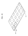
- FIG. 7E is a schematic perspective view illustrating mass production of organic light emitting devices in accordance with the invention.
- OLED organic light emitting display
- OLED is a display device comprising an array of organic light emitting diodes.
- Organic light emitting diodes are solid state devices which include an organic material and are adapted to generate and emit light when appropriate electrical potentials are applied.
- OLEDs can be generally grouped into two basic types dependent on the arrangement with which the stimulating electrical current is provided.
- Fig. 7A schematically illustrates an exploded view of a simplified structure of a passive matrix type OLED 1000.
- Fig. 7B schematically illustrates a simplified structure of an active matrix type OLED 1001.
- the OLED 1000, 1001 includes OLED pixels built over a substrate 1002, and the OLED pixels include an anode 1004, a cathode 1006 and an organic layer 1010.
- an appropriate electrical current is applied to the anode 1004
- electric current flows through the pixels and visible light is emitted from the organic layer.
- the passive matrix OLED (PMOLED) design includes elongate strips of anode 1004 arranged generally perpendicular to elongate strips of cathode 1006 with organic layers interposed therebetween.
- the intersections of the strips of cathode 1006 and anode 1004 define individual OLED pixels where light is generated and emitted upon appropriate excitation of the corresponding strips of anode 1004 and cathode 1006.
- PMOLEDs provide the advantage of relatively simple fabrication.
- the active matrix OLED includes driving circuits 1012 arranged between the substrate 1002 and an array of OLED pixels.
- An individual pixel of AMOLEDs is defined between the common cathode 1006 and an anode 1004, which is electrically isolated from other anodes.
- Each driving circuit 1012 is coupled with an anode 1004 of the OLED pixels and further coupled with a data line 1016 and a scan line 1018.
- the scan lines 1018 supply select signals that select rows of the driving circuits
- the data lines 1016 supply data signals for particular driving circuits.
- the data signals and scan signals stimulate the local driving circuits 1012, which excite the anodes 1004 so as to emit light from their corresponding pixels.
- the local driving circuits 1012, the data lines 1016 and scan lines 1018 are buried in a planarization layer 1014, which is interposed between the pixel array and the substrate 1002.
- the planarization layer 1014 provides a planar top surface on which the organic light emitting pixel array is formed.
- the planarization layer 1014 may be formed of organic or inorganic materials, and formed of two or more layers although shown as a single layer.
- the local driving circuits 1012 are typically formed with thin film transistors (TFT) and arranged in a grid or array under the OLED pixel array.
- the local driving circuits 1012 may be at least partly made of organic materials, including organic TFT.
- AMOLEDs have the advantage of fast response time improving their desirability for use in displaying data signals. Also, AMOLEDs have the advantages of consuming less power than passive matrix OLEDs.
- the substrate 1002 provides structural support for the OLED pixels and circuits.
- the substrate 1002 can comprise rigid or flexible materials as well as opaque or transparent materials, such as plastic, glass, and/or foil.
- each OLED pixel or diode is formed with the anode 1004, cathode 1006 and organic layer 1010 interposed therebetween.
- the cathode 1006 injects electrons and the anode 1004 injects holes.
- the anode 1004 and cathode 1006 are inverted; i.e., the cathode is formed on the substrate 1002 and the anode is opposingly arranged.
- Interposed between the cathode 1006 and anode 1004 are one or more organic layers. More specifically, at least one emissive or light emitting layer is interposed between the cathode 1006 and anode 1004.
- the light emitting layer may comprise one or more light emitting organic compounds. Typically, the light emitting layer is configured to emit visible light in a single color such as blue, green, red or white.
- one organic layer 1010 is formed between the cathode 1006 and anode 1004 and acts as a light emitting layer.
- Additional layers, which can be formed between the anode 1004 and cathode 1006, can include a hole transporting layer, a hole injection layer, an electron transporting layer and an electron injection layer.
- Hole transporting and/or injection layers can be interposed between the light emitting layer 1010 and the anode 1004. Electron transporting and/or injecting layers can be interposed between the cathode 1006 and the light emitting layer 1010.
- the electron injection layer facilitates injection of electrons from the cathode 1006 toward the light emitting layer 1010 by reducing the work function for injecting electrons from the cathode 1006.
- the hole injection layer facilitates injection of holes from the anode 1004 toward the light emitting layer 1010.
- the hole and electron transporting layers facilitate movement of the carriers injected from the respective electrodes toward the light emitting layer.
- a single layer may serve both electron injection and transportation functions or both hole injection and transportation functions. In some cases, one or more of these layers are lacking. In some structures, one or more organic layers are doped with one or more materials that help injection and/or transportation of the carriers. In cases where only one organic layer is formed between the cathode and anode, the organic layer may include not only an organic light emitting compound but also certain functional materials that help injection or transportation of carriers within that layer.
- organic materials that have been developed for use in these layers including the light emitting layer. Also, numerous other organic materials for use in these layers are being developed. In some configurations, these organic materials may be macromolecules including oligomers and polymers. In someinstances, the organic materials for these layers may be relatively small molecules. The skilled artisan will be able to select appropriate materials for each of these layers in view of the desired functions of the individual layers and the materials for the neighboring layers in particular designs.
- an electrical circuit provides appropriate potential between the cathode 1006 and anode 1004. This results in an electrical current flowing from the anode 1004 to the cathode 1006 via the interposed organic layer(s).
- the cathode 1006 provides electrons to the adjacent organic layer 1010.
- the anode 1004 injects holes to the organic layer 1010.
- the holes and electrons recombine in the organic layer 1010 and generate energy particles called "excitons.”
- the excitons transfer their energy to the organic light emitting material in the organic layer 1010, and the energy is used to emit visible light from the organic light emitting material.
- the spectral characteristics of light generated and emitted by the OLED 1000, 1001 depend on the nature and composition of organic molecules in the organic layer(s).
- the composition of the one or more organic layers can be selected to suit the needs of a particular application by one of ordinary skill in the art.
- OLED devices can also be categorized based on the direction of the light emission.
- a “top emission” type OLED devices emit light and display images through the cathode or top electrode 1006.
- the cathode 1006 is made of a material transparent or at least partially transparent with respect to visible light.
- the anode may be made of a material substantially reflective of the visible light.
- a second type of OLED device emits light through the anode or bottom electrode 1004 and is called a "bottom emission” type.
- the anode 1004 is made of a material which is at least partially transparent with respect to visible light.
- the cathode 1006 is made of a material substantially reflective of the visible light.
- a third type of OLED device emits light in two directions, e.g. through both anode 1004 and cathode 1006.
- the substrate may be formed of a material which is transparent, opaque or reflective of visible light.
- an OLED pixel array 1021 comprising a plurality of organic light emitting pixels is arranged over a substrate 1002 as shown in Fig. 7C.
- the pixels in the array 1021 are then controlled to be turned on and off by a driving circuit (not shown), and the plurality of the pixels as a whole displays information or image on the array 1021.
- the OLED pixel array 1021 is arranged with respect to other components, such as drive and control electronics to define a display region and a non-display region.
- the display region refers to the area of the substrate 1002 where OLED pixel array 1021 is formed.
- the non-display region refers to the remaining areas of the substrate 1002.
- the non-display region can contain logic and/or power supply circuitry. It will be understood that there will be at least portions of control/drive circuit elements arranged within the display region. For example, in PMOLEDs, conductive components will extend into the display region to provide appropriate potential to the anode and cathodes. In AMOLEDs, local driving circuits and data/scan lines coupled with the driving circuits will extend into the display region to drive and control the individual pixels of the AMOLEDs.
- FIG. 7D schematically illustrates a cross-section of an encapsulated OLED device 1011 having a layout of Fig. 7C and taken along the line d-d of Fig. 7C.
- a generally planar top plate or substrate 1061 engages with a seal 1071 which further engages with a bottom plate or substrate 1002 to enclose or encapsulate the OLED pixel array 1021.
- one or more layers are formed on the top plate 1061 or bottom plate 1002, and the seal 1071 is coupled with the bottom or top substrate 1002, 1061 via such a layer.
- the seal 1071 extends along the periphery of the OLED pixel array 1021 or the bottom or top plate 1002, 1061.
- the seal 1071 is made of a frit material as will be further discussed below.
- the top and bottom plates 1061, 1002 typically comprise materials such as plastics, glass and/or metal foils which can provide a barrier to passage of oxygen and/or water to thereby protect the OLED pixel array 1021 from exposure to these substances. At least one of the top plate 1061 and the bottom plate 1002 are typically formed of a substantially transparent material.
- seal 1071 and the top and bottom plates 1061, 1002 provide a substantially non-permeable seal to oxygen and water vapor and provide a substantially hermetically enclosed space 1081.
- the seal 1071 of a frit material in combination with the top and bottom plates 1061, 1002 provide a barrier to oxygen of less than approximately 10 -3 cc/m2 -day and to water of less than 10- 6 g/m 2 -day.
- a material that can take up oxygen and/or moisture is formed within the enclosed space 1081.
- the seal 1071 has a width W, which is its thickness in a direction parallel to a surface of the top or bottom substrate 1061, 1002 as shown in Fig. 7D.
- the width varies among devices and ranges from about 300 ⁇ m to about 3000 ⁇ m, optionally from about 500 ⁇ m to about 1500 ⁇ m. Also, the width may vary at different positions of the seal 1071. In some cases, the width of the seal 1071 is the largest where it contacts one of the bottom and top substrate 1002, 1061 or a layer formed thereon. The width may be the smallest where the seal 1071 contacts the other.
- the width variation in a single cross-section of the seal 1071 relates to the cross-sectional shape of the seal 1071 and other design parameters.
- the seal 1071 has a height H, which is its thickness in a direction perpendicular to a surface of the top or bottom substrate 1061, 1002 as shown in Fig. 7D.
- the height varies among embodiments and ranges from about 2 ⁇ m to about 30 ⁇ m, optionally from about 10 ⁇ m to about 15 ⁇ m. Generally, the height does not significantly vary at different positions of the seal 1071. However, in certain structures, the height of the seal 1071 may vary at different positions thereof.
- the seal 1071 has a generally rectangular cross-section. In other structures, however, the seal 1071 can have other various cross-sectional shapes such as a generally square cross-section, a generally trapezoidal cross-section, a cross-section with one or more rounded edges, or other configuration as indicated by the needs of a given application. To improve hermeticity, it is generally desired to increase the interfacial area where the seal 1071 directly contacts the bottom or top substrate 1002, 1061 or a layer formed thereon. In some cases, the shape of the seal can be designed such that the interfacial area can be increased.
- the seal 1071 can be arranged immediately adjacent the OLED array 1021, and in other cases, the seal 1071 is spaced some distance from the OLED array 1021.
- the seal 1071 comprises generally linear segments that are connected together to surround the OLED array 1021. Such linear segments of the seal 1071 can extend, in certain arrangements, generally parallel to respective boundaries of the OLED array 1021. In other arrangements, one or more of the linear segments of the seal 1071 are arranged in a non-parallel relationship with respective boundaries of the OLED array 1021. In yet other structures, at least part of the seal 1071 extends between the top plate 1061 and bottom plate 1002 in a curvilinear manner.
- the seal 1071 is formed using a frit material or simply "frit” or glass frit,” which includes fine glass particles.
- the frit particles includes one or more of magnesium oxide (MgO), calcium oxide (CaO), barium oxide (BaO), lithium oxide (Li 2 O), sodium oxide (Na 2 O), potassium oxide (K 2 O), boron oxide (B 2 O 3 ), vanadium oxide (V 2 O 5 ), zinc oxide (ZnO), tellurium oxide (TeO 2 ), aluminum oxide (Al 2 O 3 ), silicon dioxide (SiO 2 ), lead oxide (PbO), tin oxide (SnO), phosphorous oxide (P 2 O 5 ), ruthenium oxide (Ru 2 O), rubidium oxide (Rb 2 O), rhodium oxide (Rh 2 O), ferrite oxide (Fe 2 O 3 ), copper oxide (CuO), titanium oxide (TiO 2 ), tungsten oxide (WO 3 ), bismuth oxide (Bi 2 O
- These particles range in size from about 2 ⁇ m to about 30 ⁇ m, optionally about 5 ⁇ m to about 10 ⁇ m, although not limited only thereto.
- the particles can be as large as about the distance between the top and bottom substrates 1061, 1002 or any layers formed on these substrates where the frit seal 1071 contacts.
- the frit material used to form the seal 1071 can also include one or more filler or additive materials.
- the filler or additive materials can be provided to adjust an overall thermal expansion characteristic of the seal 1071 and/or to adjust the absorption characteristics of the seal 1071 for selected frequencies of incident radiant energy.
- the filler or additive material(s) can also include inversion and/or additive fillers to adjust a coefficient of thermal expansion of the frit.
- the filler or additive materials can include transition metals, such as chromium (Cr), iron (Fe), manganese (Mn), cobalt (Co), copper (Cu), and/or vanadium. Additional materials for the filler or additives include ZnSiO 4 , PbTiO 3 , ZrO 2 , eucryptite.
- a frit material as a dry composition typically contains glass particles from about 20 to 90 about wt%, and the remainder includes fillers and/or additives.
- the frit paste contains about 10-30 wt% organic materials and about 70-90% inorganic materials.
- the frit paste contains about 20 wt% organic materials and about 80 wt% inorganic materials.
- the organic materials may include about 0-30 wt% binder(s) and about 70-100 wt% solvent(s).
- about 10 wt% is binder(s) and about 90 wt% is solvent(s) among the organic materials.
- the inorganic materials may include about 0-10 wt% additives, about 20-40 wt% fillers and about 50-80 wt% glass powder. In some cases, about 0-5 wt% is additive(s), about 25-30 wt% is filler(s) and about 65-75 wt% is the glass powder among the inorganic materials.
- a liquid material is added to the dry frit material to form a frit paste.
- Any organic or inorganic solvent with or without additives can be used as the liquid material.
- the solvent includes one or more organic compounds.
- applicable organic compounds are ethyl cellulose, nitro cellulose, hydroxyl propyl cellulose, butyl carbitol acetate, terpineol, butyl cellusolve, acrylate compounds.
- a shape of the seal 1071 is initially formed from the frit paste and interposed between the top plate 1061 and the bottom plate 1002.
- the seal 1071 can in certain arrangements be pre-cured or pre-sintered to one of the top plate and bottom plate 1061, 1002.
- portions of the seal 1071 are selectively heated such that the frit material forming the seal 1071 at least partially melts.
- the seal 1071 is then allowed to resolidify to form a secure joint between the top plate 1061 and the bottom plate 1002 to thereby inhibit exposure of the enclosed OLED pixel array 1021 to oxygen or water.
- the selective heating of the frit seal is carried out by irradiation of light, such as a laser or directed infrared lamp.
- the frit material forming the seal 1071 can be combined with one or more additives or filler such as species selected for improved absorption of the irradiated light to facilitate heating and melting of the frit material to form the seal 1071.
- OLED devices 1011 are often mass produced.
- a plurality of separate OLED arrays 1021 is formed on a common bottom substrate 1101.
- each OLED array 1021 is surrounded by a shaped frit to form the seal 1071.
- Common top substrate (not shown) is placed over the common bottom substrate 1101 and the structures formed thereon such that the OLED arrays 1021 and the shaped frit paste are interposed between the common bottom substrate 1101 and the common top substrate.
- the OLED arrays 1021 are encapsulated and sealed, such as via the previously described enclosure process for a single OLED display device.
- the resulting product includes a plurality of OLED devices kept together by the common bottom and top substrates.
- the resulting product is cut into a plurality of pieces, each of which constitutes an OLED device 1011 of Fig. 7D.
- the individual OLED devices 1011 then further undergo additional packaging operations to further improve the sealing formed by the frit seal 1071 and the top and bottom substrates 1061, 1002.
- FIG. 1 is a cross-sectional view of an organic light emitting display according to an embodiment.
- the organic light emitting display includes a semiconductor layer 110, a gate insulating layer 120, a gate electrode 130a, a scan driver 130b, an interlayer insulating layer 140, and source and drain electrodes 150, which are disposed on a substrate 100 having a pixel region I and a non-pixel region II.
- the organic light emitting display further includes a common power supply line 150b, and a second electrode power supply line 150a, which are formed of source and drain interconnections.
- a planarization layer 160 is disposed on the entire surface of the substrate 100.
- the planarization layer 160 is formed of an organic material such as acryl-based resin or polyimide-based resin.
- the planarization layer 160 has via-holes for exposing the common power supply line 150b, the second electrode power supply line 150a, and the source and/or drain electrodes 150.
- the common power supply line 150b is partially exposed to enhance adhesive strength when the substrate is sealed using a glass frit.
- a first electrode 171 including a reflective layer 170 is disposed on the substrate 100, and a pixel defining layer 180 is disposed on the entire surface of the substrate 100.
- An organic layer 190 including at least an emission layer is disposed on the first electrode 171, and a second electrode 200 is disposed thereon.
- An encapsulation substrate 210 is disposed opposite to the substrate 100, and the substrate 100 and the encapsulation substrate 210 are sealed with a glass frit 220, thereby forming an organic light emitting display.
- the organic light emitting display includes an organic planarization layer disposed under the glass frit for sealing the substrate so that the organic planarization layer may be damaged due to a large amount of heat generated when a laser beam is radiated to the glass frit. As a result, adhesive strength at an interface in which the glass frit is adhered to the organic planarization layer may be lowered.
- FIGS. 2 to 5 are cross-sectional views of an organic light emitting display in accordance with an embodiment of the invention.
- a substrate 300 including a pixel region I, and a non-pixel region II is provided.
- the substrate 300 may be an insulating glass substrate, a plastic substrate, or a conductive substrate.
- a buffer layer 310 is formed on the surface of the substrate 300.
- the buffer layer 310 may be a silicon oxide layer, a silicon nitride layer, or a composite layer of silicon oxide and silicon nitride.
- the buffer layer 310 functions as a passivation layer for preventing impurities from out-diffusing from the substrate 300.
- a semiconductor layer 320 is formed on the buffer layer 310 in the pixel region I.
- the semiconductor layer 320 may be an amorphous silicon layer or a polysilicon layer.
- a gate insulating layer 330 is formed on the surface of the substrate 300 and the semiconductor layer 320.
- the gate insulating layer 330 may be a silicon oxide layer, a silicon nitride layer, or a composite layer of silicon oxide and silicon nitride.
- a gate electrode 340a is formed on the gate insulating layer 330 located above a portion of the semiconductor layer 320.
- the gate electrode 340a may be comprised of Al, Cu, and/or Cr.
- An interlayer insulating layer 350 is formed on the surface of the substrate 300 and the gate electrode 340a.
- the interlayer insulating layer 350 may be a silicon oxide layer, a silicon nitride layer, or a composite layer of silicon oxide and silicon nitride.
- Source and drain electrodes 360a and 360b are formed on the interlayer insulating layer 350 in the pixel region I connecting to the semiconductor layer 320 through the contact holes 351 and 352.
- the source and drain electrodes 360a and 360b may be formed of one or more materials including, for example, Mo, Cr, Al, Ti, Au, Pd and Ag.
- the electrically conductive line 360d is formed in the non-pixel region II.
- the electrically conductive line 360d may act as a common power supply line.
- a second electrode power supply line 360c may also be formed at the same time.
- a scan driver line 340b may be formed in the non-pixel region II.
- a bottom gate thin film transistor having a gate electrode disposed under a semiconductor layer may also be formed.
- the electrically conductive line in this embodiment, is formed at the same time the source and drain electrodes are formed, the electrically conductive line may also be formed at the same time the gate electrode or the first electrode is formed.
- an organic planarization layer 370 is formed on the surface of the substrate 300.
- the organic planarization layer 370 may be formed using an organic material such as acryl-based resin, polyimide-based resin, or benzocyclobutene (BCB).
- the organic planarization layer 370 is then etched to form via-holes 371a and 371b for exposing at least one of the source and/or drain electrodes 360a and 360b in the pixel region I, and the second electrode power supply line 360c in the non-pixel region II.
- the organic planarization layer 370 in the non-pixel region II, where the electrically conductive line 360d is located is removed by etching to form a recess exposing the electrically conductive line 360d.
- the glass frit is irradiated with a laser beam to adhere the substrates.
- the organic planarization layer may be damaged due to a large amount of heat generated from the laser.
- the glass frit may be delaminated from an interface with the planarization layer to decrease adhesive strength thereof. Therefore, the organic planarization layer at the edge of the substrate 300, to which the glass frit is to be adhered, is removed to prevent the above problems.
- a first electrode 380 including a reflective layer 375 is formed on the organic planarization layer 370 in the pixel region I.
- the first electrode 380 is disposed on a bottom surface of the via-hole 371 to be in contact with one of the exposed source and/or drain electrodes 360a and 360b, and extends onto the organic planarization layer 370.
- the first electrode 380 may be formed of indium tin oxide (ITO) or indium zinc oxide (IZO).
- a pixel defining layer 390 is formed on the surface of the substrate 300 including at least the first electrode 380.
- the pixel defining layer is formed to a thickness sufficient to fill the via-hole 371a, in which the first electrode 380 is disposed.
- the pixel defining layer 390 may be formed of an organic layer or an inorganic layer, preferably, an organic layer. More preferably, the pixel defining layer 390 is formed of one selected from the group including BCB, acryl-based polymer, and polyimide.
- the material comprising the pixel defining layer 390 preferably has high flowability such that the pixel defining layer can be evenly formed on the entire surface of the substrate.
- the pixel defining layer 390 is etched to form openings 395a for exposing the first electrode 380 in the pixel region I, and a portion of the second electrode power supply line 360c in the non-pixel region II.
- the pixel defining layer 390 in the non-pixel region II, at which the electrically conductive line 360d is disposed, is also removed by etching.
- an organic layer 400 is formed on the first electrode 380 exposed through the opening 395a.
- the organic layer 400 includes at least an emission layer, and may further include at least one of a hole injection layer, a hole transport layer, an electron transport layer, and an electron injection layer.
- the second electrode 410 is a transmissive electrode, and may be formed of Mg, Ag, Al, Ca, or an alloy thereof, which is transparent and has a low work function. At this time, the second electrode 410 is etched to expose the electrically conductive line 360d in the non-pixel region II.
- an encapsulation substrate 420 opposite to the substrate 300 is provided.
- the encapsulation substrate 420 may be formed of an etched insulating glass or a non-etched insulating glass.
- a glass frit 430 is applied to the edge of the encapsulation substrate 420 opposite to the substrate 300.
- the glass frit 430 may be formed of material selected from the group consisting ofinagnesium oxide (MgO), calcium oxide (CaO), barium oxide (BaO), lithium oxide (Li 2 O), sodium oxide (Na 2 O), potassium oxide (K 2 O), boron oxide (B 2 O 3 ), vanadium oxide (V 2 O 5 ), zinc oxide (ZnO), tellurium oxide (TeO 2 ), aluminum oxide (Al 2 O 3 ), silicon dioxide (SiO 2 ), lead oxide (PbO), tin oxide (SnO), phosphorous oxide (P 2 O 5 ), ruthenium oxide (Ru 2 O), rubidium oxide (Rb 2 O), rhodium oxide (Rh 2 O), ferrite oxide (Fe 2 O 3 ), copper oxide (CuO), titanium oxide (TiO 2 ) tungsten oxide (WO 3 ), bismuth oxide
- the glass frit 430 has a width larger than that of the electrically conductive line 360d. As the glass frit 430 has a larger width, the adhesive strength increases. Therefore, it is possible to protect an element from external moisture or oxygen.
- the glass frit 430 is applied on the encapsulating substrate 420. In other embodiments, the glass frit 430 may be applied on the substrate 300, or on both the substrate 300 and the encapsulation substrate 420.
- the substrate 300 and the encapsulation substrate 420 are aligned and adhered to each other. At this time, the glass frit 430 is in contact with the electrically conductive line 360d and the interlayer insulating layer 350 on the substrate 300.
- the glass frit 430 After contacting the substrate 300 with the encapsulation substrate 420 via the glass frit 430, the glass frit 430 is irradiated with a laser beam. The glass frit 430 is melted and solidified to adhere the substrate 300 and the encapsulation substrate 420, thereby completing the organic light emitting display of an embodiment.
- multiple arrays of organic light emitting pixels may be encapsulated between a single substrate 300 and a single encapsulation substrate 420 and be surrounded by additional glass frits 430 (e.g., in a mass production configuration). The multiple arrays may be cut apart resulting in individual arrays encapsulated by the substrate 300, the encapsulation substrate 420 and a glass frit 430.
- the organic planarization layer may be damaged due to the large amount of heat generated when the laser beam is radiated to the glass frit. As a result, the glass frit may be delaminated from an interface with the planarization layer to decrease adhesive strength thereof. On the other hand, if the organic planarization layer in the area of the glass frit may be removed to prevent adhesive strength of the glass frit from being lowered.
- FIG. 6 is a cross-sectional view of an organic light emitting display in accordance with a another embodiment of the present invention.
- the organic light emitting display is formed in a manner similar to the embodiment discussed above in reference to FIGS. 2-5, where a glass frit 630 is applied on an encapsulating substrate 620, and a substrate 500 is adhered to the encapsulating substrate 620.
- the glass frit 630 is then irradiated with a laser beam such that the glass frit 630 is melted and solidified, thereby completing the organic light emitting display.
- the glass frit 630 has a width equal to or smaller than that of the electrically conductive line 560d.
- the glass frit 430 was wider than the electrically conductive line 560d, and the electrically conductive line 560d substantially eclipses or totally eclipses the glass frit 630 as viewed from the substrate 300. While the wider glass frit 430 may provide increased adhesive strength compared to the glass frit 630, a narrower glass frit such as the glass frit 630 may be sufficient, depending on the embodiment.
- an organic planarization layer does not exist under the glass frit (either the glass frit 430 or the glass frit 630), it is possible to prevent the adhesive strength of either of the glass frits 430 or 630 from being lowered.
- the glass frit 630 is applied on the encapsulating substrate 620. In other embodiments, the glass frit 430 may be applied on the substrate 500, or on both the substrate 500 and the encapsulating substrate 620.
- the organic planarization layer is disposed under the glass frit for sealing the substrate so that the organic planarization layer may be damaged due to the large amount of heat generated when the laser beam is radiated to the glass frit.
- the glass frit may be delaminated from an interface with the planarization layer to decrease adhesive strength thereof.
- the organic planarization layer under the glass frit is removed to prevent adhesive strength of the glass frit from being lowered. Therefore, it is possible to prevent intrusion of external moisture or oxygen to improve reliability of an element.
- the electrically conductive line may be disposed on and under the substrate and under the glass frit.
- an organic light emitting display and a method of fabricating the same in accordance with embodiments of the present invention can prevent adhesive strength of a glass frit from being lowered when a substrate is sealed using the glass frit, thereby improving reliability.
Abstract
Description
- The present invention relates organic light emitting display devices More particularly, the present invention relates to packaging organic light emitting display devices.
- With the goal of improving upon the shortcomings of conventional displays such as cathode ray tubes, attention has recently been focused on flat panel displays such as liquid crystal displays, organic light emitting displays, plasma display panels (PDP), and so on.
- Since the liquid crystal display is a passive device rather than an emissive device, it is difficult to make having high brightness and contrast, a wide viewing angle, and a large-sized screen. While the PDP is an emissive device, it is heavy, consumes much power, and requires a complex manufacturing process, compared to other displays.
- Meanwhile, since the organic light emitting display (OLED) is an emissive device, it has a wide viewing angle, and high contrast. In addition, since it does not require a backlight, it can be made lightweight, compact, and power efficient. Further, the OLED can be driven at a low DC voltage, has a rapid response speed, and is formed entirely of solid material. As a result, the OLED has the ability to withstand external impact and a wide range of temperatures, and can be fabricated by a simple method at low cost.
- According to a first aspect of the invention, there is provided an organic light emitting device as set out in Claim 1. Preferred features of this aspect are set out in claims 2 to 16.
- According to a second aspect of the invention, there is provided an organic light emitting device as set out in Claim 17. Preferred features of this aspect are set out in claims 18 to 23.
- According to a third aspect of the invention, there is provided a method of making an organic light emitting device as set out in Claim 24. Preferred features of this aspect are set out in claims 25 to 33.
- Embodiments of the present invention will be described by way of example and with reference to the attached drawings in which:
- FIG. 1 is a cross-sectional view of an organic light emitting display according to an embodiment of the invention;
- FIGS. 2 to 5 are cross-sectional views of an organic light emitting display in accordance with another embodiment of the invention;
- FIG. 6 is a cross-sectional view of an organic light emitting display in accordance with another embodiment of the invention;
- FIG. 7A is a schematic exploded view of a passive matrix type organic light emitting display device in accordance with the invention.
- FIG 7B is a schematic exploded view of an active matrix type organic light emitting display device in accordance with the invention.
- FIG. 7C is a schematic top plan view of an organic light emitting display in accordance with the invention.
- FIG. 7D is a cross-sectional view of the organic light emitting display of FIG. 7C, taken along the line d-d.
- FIG. 7E is a schematic perspective view illustrating mass production of organic light emitting devices in accordance with the invention.
- The present invention will now be described more fully hereinafter with reference to the accompanying drawings, in which some embodiments of the invention are shown. This invention may, however, be embodied in different forms and should not be construed as limited to the embodiments set forth herein. Rather, these embodiments are provided so that this disclosure will be thorough and complete, and will fully convey the scope of the invention to those skilled in the art. In the drawings, the thickness of layers and regions may be exaggerated for clarity. Like reference numerals designate like elements throughout the specification.
- An organic light emitting display (OLED) is a display device comprising an array of organic light emitting diodes. Organic light emitting diodes are solid state devices which include an organic material and are adapted to generate and emit light when appropriate electrical potentials are applied.
- OLEDs can be generally grouped into two basic types dependent on the arrangement with which the stimulating electrical current is provided. Fig. 7A schematically illustrates an exploded view of a simplified structure of a passive
matrix type OLED 1000. Fig. 7B schematically illustrates a simplified structure of an activematrix type OLED 1001. In both configurations, the OLED 1000, 1001 includes OLED pixels built over asubstrate 1002, and the OLED pixels include ananode 1004, acathode 1006 and anorganic layer 1010. When an appropriate electrical current is applied to theanode 1004, electric current flows through the pixels and visible light is emitted from the organic layer. - Referring to Fig. 7A, the passive matrix OLED (PMOLED) design includes elongate strips of
anode 1004 arranged generally perpendicular to elongate strips ofcathode 1006 with organic layers interposed therebetween. The intersections of the strips ofcathode 1006 and anode 1004 define individual OLED pixels where light is generated and emitted upon appropriate excitation of the corresponding strips ofanode 1004 andcathode 1006. PMOLEDs provide the advantage of relatively simple fabrication. - Referring to Fig. 7B, the active matrix OLED (AMOLED) includes
driving circuits 1012 arranged between thesubstrate 1002 and an array of OLED pixels. An individual pixel of AMOLEDs is defined between thecommon cathode 1006 and ananode 1004, which is electrically isolated from other anodes. Eachdriving circuit 1012 is coupled with ananode 1004 of the OLED pixels and further coupled with adata line 1016 and ascan line 1018. In use, thescan lines 1018 supply select signals that select rows of the driving circuits, and thedata lines 1016 supply data signals for particular driving circuits. The data signals and scan signals stimulate thelocal driving circuits 1012, which excite theanodes 1004 so as to emit light from their corresponding pixels. - In the illustrated AMOLED, the
local driving circuits 1012, thedata lines 1016 andscan lines 1018 are buried in aplanarization layer 1014, which is interposed between the pixel array and thesubstrate 1002. Theplanarization layer 1014 provides a planar top surface on which the organic light emitting pixel array is formed. Theplanarization layer 1014 may be formed of organic or inorganic materials, and formed of two or more layers although shown as a single layer. Thelocal driving circuits 1012 are typically formed with thin film transistors (TFT) and arranged in a grid or array under the OLED pixel array. Thelocal driving circuits 1012 may be at least partly made of organic materials, including organic TFT. - AMOLEDs have the advantage of fast response time improving their desirability for use in displaying data signals. Also, AMOLEDs have the advantages of consuming less power than passive matrix OLEDs.
- Referring to common features of the PMOLED and AMOLED designs, the
substrate 1002 provides structural support for the OLED pixels and circuits. In various arrangements, thesubstrate 1002 can comprise rigid or flexible materials as well as opaque or transparent materials, such as plastic, glass, and/or foil. As noted above, each OLED pixel or diode is formed with theanode 1004,cathode 1006 andorganic layer 1010 interposed therebetween. When an appropriate electrical current is applied to theanode 1004, thecathode 1006 injects electrons and theanode 1004 injects holes. In certain structures, theanode 1004 andcathode 1006 are inverted; i.e., the cathode is formed on thesubstrate 1002 and the anode is opposingly arranged. - Interposed between the
cathode 1006 andanode 1004 are one or more organic layers. More specifically, at least one emissive or light emitting layer is interposed between thecathode 1006 andanode 1004. The light emitting layer may comprise one or more light emitting organic compounds. Typically, the light emitting layer is configured to emit visible light in a single color such as blue, green, red or white. In the illustrated configuration, oneorganic layer 1010 is formed between thecathode 1006 andanode 1004 and acts as a light emitting layer. Additional layers, which can be formed between theanode 1004 andcathode 1006, can include a hole transporting layer, a hole injection layer, an electron transporting layer and an electron injection layer. - Hole transporting and/or injection layers can be interposed between the light emitting
layer 1010 and theanode 1004. Electron transporting and/or injecting layers can be interposed between thecathode 1006 and thelight emitting layer 1010. The electron injection layer facilitates injection of electrons from thecathode 1006 toward thelight emitting layer 1010 by reducing the work function for injecting electrons from thecathode 1006. Similarly, the hole injection layer facilitates injection of holes from theanode 1004 toward thelight emitting layer 1010. The hole and electron transporting layers facilitate movement of the carriers injected from the respective electrodes toward the light emitting layer. - In some devices, a single layer may serve both electron injection and transportation functions or both hole injection and transportation functions. In some cases, one or more of these layers are lacking. In some structures, one or more organic layers are doped with one or more materials that help injection and/or transportation of the carriers. In cases where only one organic layer is formed between the cathode and anode, the organic layer may include not only an organic light emitting compound but also certain functional materials that help injection or transportation of carriers within that layer.
- There are numerous organic materials that have been developed for use in these layers including the light emitting layer. Also, numerous other organic materials for use in these layers are being developed. In some configurations, these organic materials may be macromolecules including oligomers and polymers. In someinstances, the organic materials for these layers may be relatively small molecules. The skilled artisan will be able to select appropriate materials for each of these layers in view of the desired functions of the individual layers and the materials for the neighboring layers in particular designs.
- In operation, an electrical circuit provides appropriate potential between the
cathode 1006 andanode 1004. This results in an electrical current flowing from theanode 1004 to thecathode 1006 via the interposed organic layer(s). In one arrangement, thecathode 1006 provides electrons to the adjacentorganic layer 1010. Theanode 1004 injects holes to theorganic layer 1010. The holes and electrons recombine in theorganic layer 1010 and generate energy particles called "excitons." The excitons transfer their energy to the organic light emitting material in theorganic layer 1010, and the energy is used to emit visible light from the organic light emitting material. The spectral characteristics of light generated and emitted by theOLED - OLED devices can also be categorized based on the direction of the light emission. In one type referred to as a "top emission" type, OLED devices emit light and display images through the cathode or
top electrode 1006. In these devices, thecathode 1006 is made of a material transparent or at least partially transparent with respect to visible light. In certain structures, to avoid losing any light that can pass through the anode orbottom electrode 1004, the anode may be made of a material substantially reflective of the visible light. A second type of OLED device emits light through the anode orbottom electrode 1004 and is called a "bottom emission" type. In the bottom emission type OLED devices, theanode 1004 is made of a material which is at least partially transparent with respect to visible light. Often, in bottom emission type OLED devices, thecathode 1006 is made of a material substantially reflective of the visible light. A third type of OLED device emits light in two directions, e.g. through bothanode 1004 andcathode 1006. Depending upon the direction(s) of the light emission, the substrate may be formed of a material which is transparent, opaque or reflective of visible light. - In many cases, an
OLED pixel array 1021 comprising a plurality of organic light emitting pixels is arranged over asubstrate 1002 as shown in Fig. 7C. The pixels in thearray 1021 are then controlled to be turned on and off by a driving circuit (not shown), and the plurality of the pixels as a whole displays information or image on thearray 1021. In certain configurations, theOLED pixel array 1021 is arranged with respect to other components, such as drive and control electronics to define a display region and a non-display region. In these structures, the display region refers to the area of thesubstrate 1002 whereOLED pixel array 1021 is formed. The non-display region refers to the remaining areas of thesubstrate 1002. The non-display region can contain logic and/or power supply circuitry. It will be understood that there will be at least portions of control/drive circuit elements arranged within the display region. For example, in PMOLEDs, conductive components will extend into the display region to provide appropriate potential to the anode and cathodes. In AMOLEDs, local driving circuits and data/scan lines coupled with the driving circuits will extend into the display region to drive and control the individual pixels of the AMOLEDs. - One design and fabrication consideration in OLED devices is that certain organic material layers of OLED devices can suffer damage or accelerated deterioration from exposure to water, oxygen or other harmful gases. Accordingly, it is generally understood that OLED devices be sealed or encapsulated to inhibit exposure to moisture and oxygen or other harmful gases found in a manufacturing or operational environment. Fig. 7D schematically illustrates a cross-section of an encapsulated
OLED device 1011 having a layout of Fig. 7C and taken along the line d-d of Fig. 7C. In this device, a generally planar top plate orsubstrate 1061 engages with aseal 1071 which further engages with a bottom plate orsubstrate 1002 to enclose or encapsulate theOLED pixel array 1021. In other variations, one or more layers are formed on thetop plate 1061 orbottom plate 1002, and theseal 1071 is coupled with the bottom ortop substrate seal 1071 extends along the periphery of theOLED pixel array 1021 or the bottom ortop plate - The
seal 1071 is made of a frit material as will be further discussed below. - The top and
bottom plates OLED pixel array 1021 from exposure to these substances. At least one of thetop plate 1061 and thebottom plate 1002 are typically formed of a substantially transparent material. - To lengthen the life time of
OLED devices 1011, it is generally desired thatseal 1071 and the top andbottom plates enclosed space 1081. In certain applications, it is indicated that theseal 1071 of a frit material in combination with the top andbottom plates enclosed space 1081, a material that can take up oxygen and/or moisture is formed within the enclosedspace 1081. - The
seal 1071 has a width W, which is its thickness in a direction parallel to a surface of the top orbottom substrate seal 1071. In some cases, the width of theseal 1071 is the largest where it contacts one of the bottom andtop substrate seal 1071 contacts the other. The width variation in a single cross-section of theseal 1071 relates to the cross-sectional shape of theseal 1071 and other design parameters. - The
seal 1071 has a height H, which is its thickness in a direction perpendicular to a surface of the top orbottom substrate seal 1071. However, in certain structures, the height of theseal 1071 may vary at different positions thereof. - In the illustrated device, the
seal 1071 has a generally rectangular cross-section. In other structures, however, theseal 1071 can have other various cross-sectional shapes such as a generally square cross-section, a generally trapezoidal cross-section, a cross-section with one or more rounded edges, or other configuration as indicated by the needs of a given application. To improve hermeticity, it is generally desired to increase the interfacial area where theseal 1071 directly contacts the bottom ortop substrate - The
seal 1071 can be arranged immediately adjacent theOLED array 1021, and in other cases, theseal 1071 is spaced some distance from theOLED array 1021. In certain cases, theseal 1071 comprises generally linear segments that are connected together to surround theOLED array 1021. Such linear segments of theseal 1071 can extend, in certain arrangements, generally parallel to respective boundaries of theOLED array 1021. In other arrangements, one or more of the linear segments of theseal 1071 are arranged in a non-parallel relationship with respective boundaries of theOLED array 1021. In yet other structures, at least part of theseal 1071 extends between thetop plate 1061 andbottom plate 1002 in a curvilinear manner. - As noted above, in certain cases, the
seal 1071 is formed using a frit material or simply "frit" or glass frit," which includes fine glass particles. The frit particles includes one or more of magnesium oxide (MgO), calcium oxide (CaO), barium oxide (BaO), lithium oxide (Li2O), sodium oxide (Na2O), potassium oxide (K2O), boron oxide (B2O3), vanadium oxide (V2O5), zinc oxide (ZnO), tellurium oxide (TeO2), aluminum oxide (Al2O3), silicon dioxide (SiO2), lead oxide (PbO), tin oxide (SnO), phosphorous oxide (P2O5), ruthenium oxide (Ru2O), rubidium oxide (Rb2O), rhodium oxide (Rh2O), ferrite oxide (Fe2O3), copper oxide (CuO), titanium oxide (TiO2), tungsten oxide (WO3), bismuth oxide (Bi2O3), antimony oxide (Sb2O3), lead-borate glass, tin-phosphate glass, vanadate glass, and borosilicate, etc. These particles range in size from about 2 µm to about 30 µm, optionally about 5 µm to about 10 µm, although not limited only thereto. The particles can be as large as about the distance between the top andbottom substrates frit seal 1071 contacts. - The frit material used to form the
seal 1071 can also include one or more filler or additive materials. The filler or additive materials can be provided to adjust an overall thermal expansion characteristic of theseal 1071 and/or to adjust the absorption characteristics of theseal 1071 for selected frequencies of incident radiant energy. The filler or additive material(s) can also include inversion and/or additive fillers to adjust a coefficient of thermal expansion of the frit. For example, the filler or additive materials can include transition metals, such as chromium (Cr), iron (Fe), manganese (Mn), cobalt (Co), copper (Cu), and/or vanadium. Additional materials for the filler or additives include ZnSiO4, PbTiO3, ZrO2, eucryptite. - A frit material as a dry composition typically contains glass particles from about 20 to 90 about wt%, and the remainder includes fillers and/or additives. In some cases, the frit paste contains about 10-30 wt% organic materials and about 70-90% inorganic materials. In some cases, the frit paste contains about 20 wt% organic materials and about 80 wt% inorganic materials. In some cases, the organic materials may include about 0-30 wt% binder(s) and about 70-100 wt% solvent(s). In some cases, about 10 wt% is binder(s) and about 90 wt% is solvent(s) among the organic materials. In some cases, the inorganic materials may include about 0-10 wt% additives, about 20-40 wt% fillers and about 50-80 wt% glass powder. In some cases, about 0-5 wt% is additive(s), about 25-30 wt% is filler(s) and about 65-75 wt% is the glass powder among the inorganic materials.
- In forming a frit seal, a liquid material is added to the dry frit material to form a frit paste. Any organic or inorganic solvent with or without additives can be used as the liquid material. Typically, the solvent includes one or more organic compounds. For example, applicable organic compounds are ethyl cellulose, nitro cellulose, hydroxyl propyl cellulose, butyl carbitol acetate, terpineol, butyl cellusolve, acrylate compounds. Then, the thus formed frit paste can be applied to form a shape of the
seal 1071 on the top and/orbottom plate - In one arrangement, a shape of the
seal 1071 is initially formed from the frit paste and interposed between thetop plate 1061 and thebottom plate 1002. Theseal 1071 can in certain arrangements be pre-cured or pre-sintered to one of the top plate andbottom plate top plate 1061 and thebottom plate 1002 with theseal 1071 interposed therebetween, portions of theseal 1071 are selectively heated such that the frit material forming theseal 1071 at least partially melts. Theseal 1071 is then allowed to resolidify to form a secure joint between thetop plate 1061 and thebottom plate 1002 to thereby inhibit exposure of the enclosedOLED pixel array 1021 to oxygen or water. - The selective heating of the frit seal is carried out by irradiation of light, such as a laser or directed infrared lamp. As previously noted, the frit material forming the
seal 1071 can be combined with one or more additives or filler such as species selected for improved absorption of the irradiated light to facilitate heating and melting of the frit material to form theseal 1071. -
OLED devices 1011 are often mass produced. In an embodiment illustrated in Fig. 7E, a plurality ofseparate OLED arrays 1021 is formed on a common bottom substrate 1101. In the illustrated arrangement, eachOLED array 1021 is surrounded by a shaped frit to form theseal 1071. Common top substrate (not shown) is placed over the common bottom substrate 1101 and the structures formed thereon such that theOLED arrays 1021 and the shaped frit paste are interposed between the common bottom substrate 1101 and the common top substrate. TheOLED arrays 1021 are encapsulated and sealed, such as via the previously described enclosure process for a single OLED display device. The resulting product includes a plurality of OLED devices kept together by the common bottom and top substrates. Then, the resulting product is cut into a plurality of pieces, each of which constitutes anOLED device 1011 of Fig. 7D. Theindividual OLED devices 1011 then further undergo additional packaging operations to further improve the sealing formed by thefrit seal 1071 and the top andbottom substrates - FIG. 1 is a cross-sectional view of an organic light emitting display according to an embodiment. Referring to FIG. 1, the organic light emitting display includes a
semiconductor layer 110, agate insulating layer 120, agate electrode 130a, ascan driver 130b, aninterlayer insulating layer 140, and source and drainelectrodes 150, which are disposed on asubstrate 100 having a pixel region I and a non-pixel region II. In addition, the organic light emitting display further includes a commonpower supply line 150b, and a second electrodepower supply line 150a, which are formed of source and drain interconnections. - A
planarization layer 160 is disposed on the entire surface of thesubstrate 100. Theplanarization layer 160 is formed of an organic material such as acryl-based resin or polyimide-based resin. Theplanarization layer 160 has via-holes for exposing the commonpower supply line 150b, the second electrodepower supply line 150a, and the source and/or drainelectrodes 150. The commonpower supply line 150b is partially exposed to enhance adhesive strength when the substrate is sealed using a glass frit. - A
first electrode 171 including areflective layer 170 is disposed on thesubstrate 100, and apixel defining layer 180 is disposed on the entire surface of thesubstrate 100. Anorganic layer 190 including at least an emission layer is disposed on thefirst electrode 171, and asecond electrode 200 is disposed thereon. Anencapsulation substrate 210 is disposed opposite to thesubstrate 100, and thesubstrate 100 and theencapsulation substrate 210 are sealed with aglass frit 220, thereby forming an organic light emitting display. - However, in the foregoing embodiment, the organic light emitting display includes an organic planarization layer disposed under the glass frit for sealing the substrate so that the organic planarization layer may be damaged due to a large amount of heat generated when a laser beam is radiated to the glass frit. As a result, adhesive strength at an interface in which the glass frit is adhered to the organic planarization layer may be lowered.
- FIGS. 2 to 5 are cross-sectional views of an organic light emitting display in accordance with an embodiment of the invention. Referring to FIG. 2, a
substrate 300 including a pixel region I, and a non-pixel region II is provided. Thesubstrate 300 may be an insulating glass substrate, a plastic substrate, or a conductive substrate. - A
buffer layer 310 is formed on the surface of thesubstrate 300. Thebuffer layer 310 may be a silicon oxide layer, a silicon nitride layer, or a composite layer of silicon oxide and silicon nitride. In one aspect, thebuffer layer 310 functions as a passivation layer for preventing impurities from out-diffusing from thesubstrate 300. - A
semiconductor layer 320 is formed on thebuffer layer 310 in the pixel region I. Thesemiconductor layer 320 may be an amorphous silicon layer or a polysilicon layer. Agate insulating layer 330 is formed on the surface of thesubstrate 300 and thesemiconductor layer 320. Thegate insulating layer 330 may be a silicon oxide layer, a silicon nitride layer, or a composite layer of silicon oxide and silicon nitride. - After forming the
gate insulating layer 330, agate electrode 340a is formed on thegate insulating layer 330 located above a portion of thesemiconductor layer 320. Thegate electrode 340a may be comprised of Al, Cu, and/or Cr. - An interlayer insulating
layer 350 is formed on the surface of thesubstrate 300 and thegate electrode 340a. The interlayer insulatinglayer 350 may be a silicon oxide layer, a silicon nitride layer, or a composite layer of silicon oxide and silicon nitride. - The interlayer insulating
layer 350 and thegate insulating layer 330 in the pixel region I are then etched to form contact holes 351 and 352 for exposing thesemiconductor layer 320. Source anddrain electrodes interlayer insulating layer 350 in the pixel region I connecting to thesemiconductor layer 320 through the contact holes 351 and 352. The source anddrain electrodes - Further, at the same time the source and
drain electrodes conductive line 360d is formed in the non-pixel region II. The electricallyconductive line 360d may act as a common power supply line. In addition, a second electrodepower supply line 360c may also be formed at the same time. Furthermore, at the same time thegate electrode 340a is formed, ascan driver line 340b may be formed in the non-pixel region II. - While a top gate thin film transistor configuration is described in this embodiment, a bottom gate thin film transistor having a gate electrode disposed under a semiconductor layer may also be formed. In addition, while the electrically conductive line, in this embodiment, is formed at the same time the source and drain electrodes are formed, the electrically conductive line may also be formed at the same time the gate electrode or the first electrode is formed.
- Referring to FIG. 3, an
organic planarization layer 370 is formed on the surface of thesubstrate 300. Theorganic planarization layer 370 may be formed using an organic material such as acryl-based resin, polyimide-based resin, or benzocyclobutene (BCB). Theorganic planarization layer 370 is then etched to form via-holes drain electrodes power supply line 360c in the non-pixel region II. - In addition, the
organic planarization layer 370 in the non-pixel region II, where the electricallyconductive line 360d is located, is removed by etching to form a recess exposing the electricallyconductive line 360d. When the substrate is sealed using a glass frit, the glass frit is irradiated with a laser beam to adhere the substrates. At this time, if the organic planarization layer still existed under the glass frit, the planarization layer may be damaged due to a large amount of heat generated from the laser. As a result, the glass frit may be delaminated from an interface with the planarization layer to decrease adhesive strength thereof. Therefore, the organic planarization layer at the edge of thesubstrate 300, to which the glass frit is to be adhered, is removed to prevent the above problems. - Referring to FIG. 4, a
first electrode 380 including areflective layer 375 is formed on theorganic planarization layer 370 in the pixel region I. Thefirst electrode 380 is disposed on a bottom surface of the via-hole 371 to be in contact with one of the exposed source and/ordrain electrodes organic planarization layer 370. Thefirst electrode 380 may be formed of indium tin oxide (ITO) or indium zinc oxide (IZO). - After forming the
first electrode 380, apixel defining layer 390 is formed on the surface of thesubstrate 300 including at least thefirst electrode 380. The pixel defining layer is formed to a thickness sufficient to fill the via-hole 371a, in which thefirst electrode 380 is disposed. Thepixel defining layer 390 may be formed of an organic layer or an inorganic layer, preferably, an organic layer. More preferably, thepixel defining layer 390 is formed of one selected from the group including BCB, acryl-based polymer, and polyimide. The material comprising thepixel defining layer 390 preferably has high flowability such that the pixel defining layer can be evenly formed on the entire surface of the substrate. - At this time, the
pixel defining layer 390 is etched to formopenings 395a for exposing thefirst electrode 380 in the pixel region I, and a portion of the second electrodepower supply line 360c in the non-pixel region II. In addition, thepixel defining layer 390 in the non-pixel region II, at which the electricallyconductive line 360d is disposed, is also removed by etching. - After forming the
pixel defining layer 390 and etching theopening 395a, anorganic layer 400 is formed on thefirst electrode 380 exposed through theopening 395a. Theorganic layer 400 includes at least an emission layer, and may further include at least one of a hole injection layer, a hole transport layer, an electron transport layer, and an electron injection layer. - Next, a
second electrode 410 is formed on the surface of thesubstrate 300. Thesecond electrode 410 is a transmissive electrode, and may be formed of Mg, Ag, Al, Ca, or an alloy thereof, which is transparent and has a low work function. At this time, thesecond electrode 410 is etched to expose the electricallyconductive line 360d in the non-pixel region II. - Referring to FIG. 5, an
encapsulation substrate 420 opposite to thesubstrate 300 is provided. Theencapsulation substrate 420 may be formed of an etched insulating glass or a non-etched insulating glass. - In this embodiment, a
glass frit 430 is applied to the edge of theencapsulation substrate 420 opposite to thesubstrate 300. Theglass frit 430 may be formed of material selected from the group consisting ofinagnesium oxide (MgO), calcium oxide (CaO), barium oxide (BaO), lithium oxide (Li2O), sodium oxide (Na2O), potassium oxide (K2O), boron oxide (B2O3), vanadium oxide (V2O5), zinc oxide (ZnO), tellurium oxide (TeO2), aluminum oxide (Al2O3), silicon dioxide (SiO2), lead oxide (PbO), tin oxide (SnO), phosphorous oxide (P2O5), ruthenium oxide (Ru2O), rubidium oxide (Rb2O), rhodium oxide (Rh2O), ferrite oxide (Fe2O3), copper oxide (CuO), titanium oxide (TiO2) tungsten oxide (WO3), bismuth oxide (Bi2O3), antimony oxide (Sb2O3), lead-borate glass, tin-phosphate glass, vanadate glass, and borosilicate, and a composite thereof. Theglass frit 430 may be applied by a dispensing method or a screen printing method. - In the example shown in Figure 5, the
glass frit 430 has a width larger than that of the electricallyconductive line 360d. As theglass frit 430 has a larger width, the adhesive strength increases. Therefore, it is possible to protect an element from external moisture or oxygen. In this embodiment, theglass frit 430 is applied on the encapsulatingsubstrate 420. In other embodiments, theglass frit 430 may be applied on thesubstrate 300, or on both thesubstrate 300 and theencapsulation substrate 420. - After applying the
glass frit 430, thesubstrate 300 and theencapsulation substrate 420 are aligned and adhered to each other. At this time, theglass frit 430 is in contact with the electricallyconductive line 360d and the interlayer insulatinglayer 350 on thesubstrate 300. - After contacting the
substrate 300 with theencapsulation substrate 420 via theglass frit 430, theglass frit 430 is irradiated with a laser beam. Theglass frit 430 is melted and solidified to adhere thesubstrate 300 and theencapsulation substrate 420, thereby completing the organic light emitting display of an embodiment. - It should be noted, that while the example described above in reference to FIGS. 2-5 showed a single organic light emitting pixel being encapsulated, similar procedures may be used to encapsulate an array of organic light emitting pixels. Additionally, multiple arrays of organic light emitting pixels may be encapsulated between a
single substrate 300 and asingle encapsulation substrate 420 and be surrounded by additional glass frits 430 (e.g., in a mass production configuration). The multiple arrays may be cut apart resulting in individual arrays encapsulated by thesubstrate 300, theencapsulation substrate 420 and aglass frit 430. - As described above, if the organic planarization layer is disposed under the glass frit for sealing the substrate, the organic planarization layer may be damaged due to the large amount of heat generated when the laser beam is radiated to the glass frit. As a result, the glass frit may be delaminated from an interface with the planarization layer to decrease adhesive strength thereof. On the other hand, if the organic planarization layer in the area of the glass frit may be removed to prevent adhesive strength of the glass frit from being lowered.
- FIG. 6 is a cross-sectional view of an organic light emitting display in accordance with a another embodiment of the present invention. Referring to FIG. 6, the organic light emitting display is formed in a manner similar to the embodiment discussed above in reference to FIGS. 2-5, where a
glass frit 630 is applied on an encapsulatingsubstrate 620, and asubstrate 500 is adhered to the encapsulatingsubstrate 620. Theglass frit 630 is then irradiated with a laser beam such that theglass frit 630 is melted and solidified, thereby completing the organic light emitting display. - In this embodiment, the
glass frit 630 has a width equal to or smaller than that of the electricallyconductive line 560d. In the embodiment shown in FIG. 5, theglass frit 430 was wider than the electricallyconductive line 560d, and the electricallyconductive line 560d substantially eclipses or totally eclipses theglass frit 630 as viewed from thesubstrate 300. While thewider glass frit 430 may provide increased adhesive strength compared to theglass frit 630, a narrower glass frit such as theglass frit 630 may be sufficient, depending on the embodiment. In addition, since an organic planarization layer does not exist under the glass frit (either theglass frit 430 or the glass frit 630), it is possible to prevent the adhesive strength of either of the glass frits 430 or 630 from being lowered. - In this embodiment, the
glass frit 630 is applied on the encapsulatingsubstrate 620. In other embodiments, theglass frit 430 may be applied on thesubstrate 500, or on both thesubstrate 500 and the encapsulatingsubstrate 620. - As described above, in embodiments where the organic planarization layer is disposed under the glass frit for sealing the substrate so that the organic planarization layer may be damaged due to the large amount of heat generated when the laser beam is radiated to the glass frit. As a result, the glass frit may be delaminated from an interface with the planarization layer to decrease adhesive strength thereof. However, in other embodiments, the organic planarization layer under the glass frit is removed to prevent adhesive strength of the glass frit from being lowered. Therefore, it is possible to prevent intrusion of external moisture or oxygen to improve reliability of an element.
- While the foregoing embodiments of the present invention exemplarily describe the electrically conductive line positioned at both sides of the substrate and disposed under the glass frit, the electrically conductive line may be disposed on and under the substrate and under the glass frit.
- As can be seen from the foregoing, an organic light emitting display and a method of fabricating the same in accordance with embodiments of the present invention can prevent adhesive strength of a glass frit from being lowered when a substrate is sealed using the glass frit, thereby improving reliability.
- Although the present invention has been described with reference to certain embodiments thereof, it will be understood by those skilled in the art that a variety of modifications and variations may be made to the present invention without departing from the scope of the present invention defined in the appended claims, and their equivalents.
Claims (33)
- An organic light emitting device comprising:a first substrate comprising a pixel region and a non-pixel region;an array of organic light emitting pixels formed over the pixel region of the first substrate;a second substrate placed over the first substrate, the array being interposed between the first and second substrates;an electrically conductive line formed over the non-pixel region of the first substrate; anda frit seal interposed between the first and second substrates and surrounding the array such that the array is encapsulated by the first substrate, the second substrate and the frit seal, wherein the electrically conductive line comprises a portion overlapping the frit seal in a segment of the device such that the portion of the electrically conductive line substantially eclipses the frit seal when viewed from the first substrate.
- A device according to Claim 1, wherein the portion of the electrically conductive line substantially totally eclipses the frit seal when viewed from the first substrate.
- A device according to Claim 1 or 2, wherein the frit seal contacts the electrically conductive line.
- A device according to any one of Claims 1 to 3, wherein there is substantially no material between the frit seal and the electrically conductive line.
- A device according to any one of Claims 1 to 4, wherein the device further comprises at least one layer located between the electrically conductive line and the first substrate, the at least one layer comprising an organic material.
- A device according to any one of Claims 1 to 5, wherein the electrically conductive line further comprises a portion that does not overlap the frit seal.
- A device according to any one of Claims 1 to 6, wherein the electrically conductive line extends along a peripheral edge of the first substrate, and wherein the frit seal extends along the peripheral edge of the first edge.
- A device according to any one of Claims 1 to 7, wherein the electrically conductive line is made of metal.
- A device according to any one of Claims 1 to 8, wherein in another segment of the device, the frit seal further comprises a non-eclipsed portion that is not eclipsed by the electrically conductive line when viewed from the first substrate.
- A device according to any one of Claims 1 to 9, wherein the frit seal has a width taken in a cross-sectional plane, and the electrically conductive line has a width taken in the cross-sectional plane, and wherein the width of the frit seal is substantially smaller than the width of the electrically conductive line.
- A device according to any one of Claims 1 to 10, wherein the electrically conductive line comprises a power supply line electrically connected to the array.
- A device according to any one of Claims 1 to 11, wherein the electrically conductive line comprises a portion overlapping the frit seal in substantially throughout the device such that the portion of the electrically conductive line substantially eclipses the frit seal when viewed from the first substrate.
- A device according to any one of Claims 1 to 12, further comprising a planarization layer formed over at least part of the non-pixel region of the first substrate,
wherein the frit seal does not contact the planarization layer. - A device according to any one of Claims 1 to 13, further comprising an organic or inorganic planarization layer formed over at least part of the non-pixel region of the first substrate, wherein the organic planarization layer comprises a recess exposing the electrically conductive line.
- A device according to any one of Claims 1 to 14, further comprising a plurality of thin film transistors interposed between the first substrate and the array,
wherein the electrically conductive line is made of a material used in the plurality of thin film transistors. - A device according to any one of Claims 1 to 15, wherein the frit seal comprises one or more materials selected from the group consisting of magnesium oxide (MgO), calcium oxide (CaO), barium oxide (BaO), lithium oxide (Li2O), sodium oxide (Na2O), potassium oxide (K2O), boron oxide (B2O3), vanadium oxide (V2O5), zinc oxide (ZnO), tellurium oxide (TeO2), aluminum oxide (Al2O3), silicon dioxide (SiO2), lead oxide (PbO), tin oxide (SnO), phosphorous oxide (P2O5), ruthenium oxide (Ru2O), rubidium oxide (Rb2O), rhodium oxide (Rh2O), ferrite oxide (Fe2O3), copper oxide (CuO), titanium oxide (TiO2), tungsten oxide (WO3), bismuth oxide (Bi2O3), antimony oxide (Sb2O3), lead-borate glass, tin-phosphate glass, vanadate glass, and borosilicate.
- An organic light emitting device comprising:a first substrate defining comprising a pixel region and a non-pixel region;an array of organic light emitting pixels formed over the pixel region of the first substrate;a second substrate placed over the first substrate, the array being interposed between the first and second substrates;a frit seal interposed between the first and second substrates and surrounding the array such that the array is encapsulated by the first substrate, the second substrate and the frit seal; anda planarization layer formed over the first substrate, wherein the frit seal does not contact the planarization layer.
- A device according to Claim 17, wherein the planarization layer comprises a recess, and wherein at least part of the first seal extends into the recess.
- A device according to Claim 17 or 18, wherein the planarization layer extends over at least part of the pixel region and at least part of the non-pixel region.
- A device according to any one of Claims 17 to 19, wherein the planarization layer comprises an organic material.
- A device according to any one of Claims 17 to 19, wherein the planarization layer comprises an inorganic material.
- A device according to any one of Claims 17 to 21, further comprising an electrically conductive line formed over the non-pixel region of the first substrate, wherein the electrically conductive line comprises a portion overlapping the frit seal in a segment of the device such that the portion of the electrically conductive line substantially eclipses the frit seal when viewed from the first substrate.
- A device according to Claim 22, wherein the planarization layer does not contact the overlapping portion of the electrically conductive line.
- A method of making an organic light emitting device, the method comprising:providing an unfinished device comprising a first substrate, an array of organic light emitting pixels formed over the first substrate, and an electrically conductive line formed over the first substrate and not overlapping the array;further providing a second substrate;interposing a frit between the first and second substrates such that the array is interposed between the first and second substrates, that the frit surrounds the array and that a portion of the electrically conductive line overlaps the frit in a segment of the device, whereby the portion of the electrically conductive line substantially eclipses the frit in the segment; andmelting and resolidifying at least part of the frit so as to interconnect the unfinished device and the second substrate via the frit, wherein the frit connects to the electrically conductive line with or without a material therebetween, and wherein the frit connects to the second substrate with or without a material therebetween.
- A method according to Claim 24, wherein interposing comprises contacting the frit with the portion of the electrically conductive line and the second substrate.
- A method according to Claim 24 or 25, wherein the unfinished device further comprises a planarization layer generally formed over the electrically conductive line with an opening exposing part of the conductive line, and wherein interposing the frit comprises contacting the frit with the electrically conductive line through the opening.
- A method according to Claim 26, wherein providing the unfinished device comprises:providing the planarization layer over the electrically conductive line; andselectively etching the planarization layer to form the opening.
- A method according to any one of Claims 24 to 27, wherein the melting comprises irradiating a laser beam or infrared ray to at least part of the frit.
- A method according to any one of Claims 24 to 28, wherein interposing the frit comprises:forming the frit over at least one of the first and second substrates; andarranging the first and second substrate so as to interpose the frit therebetween.
- A method according to Claim 29, wherein forming the frit comprises screen-printing or dispensing a material of the frit over at least one of the first and second substrates.
- A method according to any one of Claims 24 to 30, wherein the unfinished device further comprises one or more additional arrays of organic light emitting pixels and one or more additional electrically conductive lines formed over the first substrate;
wherein the method further comprises forming one or more additional frits between the first and second substrates such that each additional frit surrounds one of the additional arrays and contacts a portion of one of the additional electrically conductive lines. - A method according to Claim 31, wherein the one of the additional electrically conductive lines substantially eclipses the additional frit.
- A method according to Claim 31 or 32, further comprising cutting the resulting product of Claim 31 into two or more pieces, wherein one of the pieces comprises the frit and the array interposed between the first and second substrate.
Applications Claiming Priority (3)
| Application Number | Priority Date | Filing Date | Title |
|---|---|---|---|
| KR1020060007025A KR100635514B1 (en) | 2006-01-23 | 2006-01-23 | Organic electroluminescence display device and method for fabricating of the same |
| KR20060007962 | 2006-01-25 | ||
| KR1020060027321A KR100712185B1 (en) | 2006-01-25 | 2006-03-27 | Organic electroluminescence display device and method for fabricating of the same |
Publications (3)
| Publication Number | Publication Date |
|---|---|
| EP1811570A2 true EP1811570A2 (en) | 2007-07-25 |
| EP1811570A3 EP1811570A3 (en) | 2011-02-02 |
| EP1811570B1 EP1811570B1 (en) | 2020-11-25 |
Family
ID=37913127
Family Applications (1)
| Application Number | Title | Priority Date | Filing Date |
|---|---|---|---|
| EP07250267.7A Active EP1811570B1 (en) | 2006-01-23 | 2007-01-23 | Organic light emitting display and method of fabricating the same |
Country Status (1)
| Country | Link |
|---|---|
| EP (1) | EP1811570B1 (en) |
Cited By (7)
| Publication number | Priority date | Publication date | Assignee | Title |
|---|---|---|---|---|
| EP1814158A2 (en) * | 2006-01-27 | 2007-08-01 | Samsung SDI Co., Ltd. | Flat panel display device and method of making the same |
| US7948177B2 (en) | 2006-01-27 | 2011-05-24 | Samsung Mobile Display Co., Ltd. | Flat panel display device with protective layer structure and method of making the same |
| US7992411B2 (en) | 2008-05-30 | 2011-08-09 | Corning Incorporated | Method for sintering a frit to a glass plate |
| US8147632B2 (en) | 2008-05-30 | 2012-04-03 | Corning Incorporated | Controlled atmosphere when sintering a frit to a glass plate |
| US9761827B2 (en) | 2011-11-29 | 2017-09-12 | Semiconductor Energy Laboratory Co., Ltd. | Sealed structure, light-emitting device, electronic device, and lighting device |
| US10068926B2 (en) | 2011-05-05 | 2018-09-04 | Semiconductor Energy Laboratory Co., Ltd. | Semiconductor device and method for manufacturing the same |
| EP3734662A4 (en) * | 2018-09-14 | 2021-03-03 | Yungu (Gu'an) Technology Co., Ltd. | Display panel, display screen, and display terminal |
Citations (3)
| Publication number | Priority date | Publication date | Assignee | Title |
|---|---|---|---|---|
| JPH1074583A (en) | 1996-08-30 | 1998-03-17 | Sanyo Electric Co Ltd | Organic el display and manufacture of organic el display |
| US20040207314A1 (en) | 2003-04-16 | 2004-10-21 | Aitken Bruce G. | Glass package that is hermetically sealed with a frit and method of fabrication |
| EP1575090A2 (en) | 2004-03-09 | 2005-09-14 | Samsung SDI Co., Ltd. | Electroluminescence display device |
Family Cites Families (2)
| Publication number | Priority date | Publication date | Assignee | Title |
|---|---|---|---|---|
| KR100544123B1 (en) * | 2003-07-29 | 2006-01-23 | 삼성에스디아이 주식회사 | Flat panel display |
| KR100615212B1 (en) * | 2004-03-08 | 2006-08-25 | 삼성에스디아이 주식회사 | Flat display device |
-
2007
- 2007-01-23 EP EP07250267.7A patent/EP1811570B1/en active Active
Patent Citations (3)
| Publication number | Priority date | Publication date | Assignee | Title |
|---|---|---|---|---|
| JPH1074583A (en) | 1996-08-30 | 1998-03-17 | Sanyo Electric Co Ltd | Organic el display and manufacture of organic el display |
| US20040207314A1 (en) | 2003-04-16 | 2004-10-21 | Aitken Bruce G. | Glass package that is hermetically sealed with a frit and method of fabrication |
| EP1575090A2 (en) | 2004-03-09 | 2005-09-14 | Samsung SDI Co., Ltd. | Electroluminescence display device |
Cited By (14)
| Publication number | Priority date | Publication date | Assignee | Title |
|---|---|---|---|---|
| US8035300B2 (en) | 2006-01-27 | 2011-10-11 | Samsung Mobile Display Co., Ltd. | Flat panel display device and method of making the same |
| EP1814158A3 (en) * | 2006-01-27 | 2007-10-03 | Samsung SDI Co., Ltd. | Flat panel display device and method of making the same |
| US7948177B2 (en) | 2006-01-27 | 2011-05-24 | Samsung Mobile Display Co., Ltd. | Flat panel display device with protective layer structure and method of making the same |
| EP1814158A2 (en) * | 2006-01-27 | 2007-08-01 | Samsung SDI Co., Ltd. | Flat panel display device and method of making the same |
| US8147976B2 (en) | 2008-05-30 | 2012-04-03 | Corning Incorporated | Sealed glass package |
| US8147632B2 (en) | 2008-05-30 | 2012-04-03 | Corning Incorporated | Controlled atmosphere when sintering a frit to a glass plate |
| US7992411B2 (en) | 2008-05-30 | 2011-08-09 | Corning Incorporated | Method for sintering a frit to a glass plate |
| US8329303B2 (en) | 2008-05-30 | 2012-12-11 | Corning Incorporated | Controlled atmosphere when sintering a frit to a glass plate |
| US10068926B2 (en) | 2011-05-05 | 2018-09-04 | Semiconductor Energy Laboratory Co., Ltd. | Semiconductor device and method for manufacturing the same |
| US10283530B2 (en) | 2011-05-05 | 2019-05-07 | Semiconductor Energy Laboratory Co., Ltd. | Semiconductor device and method for manufacturing the same |
| US11942483B2 (en) | 2011-05-05 | 2024-03-26 | Semiconductor Energy Laboratory Co., Ltd. | Semiconductor device and method for manufacturing the same |
| US9761827B2 (en) | 2011-11-29 | 2017-09-12 | Semiconductor Energy Laboratory Co., Ltd. | Sealed structure, light-emitting device, electronic device, and lighting device |
| EP3734662A4 (en) * | 2018-09-14 | 2021-03-03 | Yungu (Gu'an) Technology Co., Ltd. | Display panel, display screen, and display terminal |
| US11362146B2 (en) | 2018-09-14 | 2022-06-14 | Yungu (Gu'an) Technology Co., Ltd. | Display panel, display screen, and display terminal with plurality of film layer and multiple optical lengths |
Also Published As
| Publication number | Publication date |
|---|---|
| EP1811570B1 (en) | 2020-11-25 |
| EP1811570A3 (en) | 2011-02-02 |
Similar Documents
| Publication | Publication Date | Title |
|---|---|---|
| US8164257B2 (en) | Organic light emitting display and method of fabricating the same | |
| US8026511B2 (en) | Organic light emitting display device and method of fabricating the same | |
| EP1811571B1 (en) | Organic light emitting display and method of fabricating the same | |
| US7837530B2 (en) | Method of sealing an organic light emitting display by means of a glass frit seal assembly | |
| EP1814174B1 (en) | Organic light-emitting display device and method for fabricating the same | |
| US7999372B2 (en) | Organic light emitting display device and method of fabricating the same | |
| EP1814176B1 (en) | Organic light-emitting display device and method for fabricating the same | |
| US8038495B2 (en) | Organic light-emitting display device and manufacturing method of the same | |
| EP1811588A2 (en) | Organic light emitting display and method of fabricating the same | |
| US8729796B2 (en) | Organic light emitting display device including a gap to improve image quality and method of fabricating the same | |
| US8125146B2 (en) | Organic light emitting display having a second frit portion configured to melt more easily than a frit portion | |
| US7825594B2 (en) | Organic light emitting display and fabricating method of the same | |
| EP1814177B1 (en) | Oganic light-emitting display device and method for fabricating the same | |
| EP1814184B1 (en) | Organic light emitting display device and a method of manufacturing thereof | |
| EP1814178A2 (en) | Organic light-emitting display with frit seal and reinforcing structure bonded to frame | |
| EP1814175B1 (en) | Organic light emitting display device and a method of manufacturing thereof | |
| EP1814183A2 (en) | Organic light-emitting display device | |
| EP1811570B1 (en) | Organic light emitting display and method of fabricating the same | |
| US8796920B2 (en) | Organic light emitting display and fabricating method of the same |
Legal Events
| Date | Code | Title | Description |
|---|---|---|---|
| PUAI | Public reference made under article 153(3) epc to a published international application that has entered the european phase |
Free format text: ORIGINAL CODE: 0009012 |
|
| 17P | Request for examination filed |
Effective date: 20070129 |
|
| AK | Designated contracting states |
Kind code of ref document: A2 Designated state(s): AT BE BG CH CY CZ DE DK EE ES FI FR GB GR HU IE IS IT LI LT LU LV MC NL PL PT RO SE SI SK TR |
|
| AX | Request for extension of the european patent |
Extension state: AL BA HR MK YU |
|
| RAP1 | Party data changed (applicant data changed or rights of an application transferred) |
Owner name: SAMSUNG MOBILE DISPLAY CO., LTD. |
|
| PUAL | Search report despatched |
Free format text: ORIGINAL CODE: 0009013 |
|
| AK | Designated contracting states |
Kind code of ref document: A3 Designated state(s): AT BE BG CH CY CZ DE DK EE ES FI FR GB GR HU IE IS IT LI LT LU LV MC NL PL PT RO SE SI SK TR |
|
| AX | Request for extension of the european patent |
Extension state: AL BA HR MK RS |
|
| AKX | Designation fees paid |
Designated state(s): DE FR GB |
|
| RAP1 | Party data changed (applicant data changed or rights of an application transferred) |
Owner name: SAMSUNG DISPLAY CO., LTD. |
|
| 17Q | First examination report despatched |
Effective date: 20131003 |
|
| RAP1 | Party data changed (applicant data changed or rights of an application transferred) |
Owner name: SAMSUNG DISPLAY CO., LTD. |
|
| STAA | Information on the status of an ep patent application or granted ep patent |
Free format text: STATUS: EXAMINATION IS IN PROGRESS |
|
| GRAP | Despatch of communication of intention to grant a patent |
Free format text: ORIGINAL CODE: EPIDOSNIGR1 |
|
| STAA | Information on the status of an ep patent application or granted ep patent |
Free format text: STATUS: GRANT OF PATENT IS INTENDED |
|
| INTG | Intention to grant announced |
Effective date: 20200619 |
|
| GRAS | Grant fee paid |
Free format text: ORIGINAL CODE: EPIDOSNIGR3 |
|
| GRAA | (expected) grant |
Free format text: ORIGINAL CODE: 0009210 |
|
| STAA | Information on the status of an ep patent application or granted ep patent |
Free format text: STATUS: THE PATENT HAS BEEN GRANTED |
|
| REG | Reference to a national code |
Ref country code: DE Ref legal event code: R081 Ref document number: 602007060796 Country of ref document: DE Owner name: SAMSUNG DISPLAY CO., LTD., YONGIN-SI, KR Free format text: FORMER OWNER: SAMSUNG SDI CO., LTD., SUWON, KYONGGI-DO, KR |
|
| AK | Designated contracting states |
Kind code of ref document: B1 Designated state(s): DE FR GB |
|
| REG | Reference to a national code |
Ref country code: GB Ref legal event code: FG4D |
|
| REG | Reference to a national code |
Ref country code: DE Ref legal event code: R096 Ref document number: 602007060796 Country of ref document: DE |
|
| REG | Reference to a national code |
Ref country code: DE Ref legal event code: R097 Ref document number: 602007060796 Country of ref document: DE |
|
| PLBE | No opposition filed within time limit |
Free format text: ORIGINAL CODE: 0009261 |
|
| STAA | Information on the status of an ep patent application or granted ep patent |
Free format text: STATUS: NO OPPOSITION FILED WITHIN TIME LIMIT |
|
| 26N | No opposition filed |
Effective date: 20210826 |
|
| REG | Reference to a national code |
Ref country code: DE Ref legal event code: R079 Ref document number: 602007060796 Country of ref document: DE Free format text: PREVIOUS MAIN CLASS: H01L0027320000 Ipc: H10K0059000000 |
|
| PGFP | Annual fee paid to national office [announced via postgrant information from national office to epo] |
Ref country code: DE Payment date: 20221220 Year of fee payment: 17 |
|
| P01 | Opt-out of the competence of the unified patent court (upc) registered |
Effective date: 20230515 |
|
| PGFP | Annual fee paid to national office [announced via postgrant information from national office to epo] |
Ref country code: GB Payment date: 20231220 Year of fee payment: 18 |
|
| PGFP | Annual fee paid to national office [announced via postgrant information from national office to epo] |
Ref country code: FR Payment date: 20231222 Year of fee payment: 18 |