EP1830252A2 - Specialised processing block for programmable logic device - Google Patents
Specialised processing block for programmable logic device Download PDFInfo
- Publication number
- EP1830252A2 EP1830252A2 EP07002429A EP07002429A EP1830252A2 EP 1830252 A2 EP1830252 A2 EP 1830252A2 EP 07002429 A EP07002429 A EP 07002429A EP 07002429 A EP07002429 A EP 07002429A EP 1830252 A2 EP1830252 A2 EP 1830252A2
- Authority
- EP
- European Patent Office
- Prior art keywords
- circuitry
- rounding
- processing block
- specialized processing
- circuit board
- Prior art date
- Legal status (The legal status is an assumption and is not a legal conclusion. Google has not performed a legal analysis and makes no representation as to the accuracy of the status listed.)
- Withdrawn
Links
Images


Classifications
-
- G—PHYSICS
- G06—COMPUTING; CALCULATING OR COUNTING
- G06F—ELECTRIC DIGITAL DATA PROCESSING
- G06F7/00—Methods or arrangements for processing data by operating upon the order or content of the data handled
- G06F7/38—Methods or arrangements for performing computations using exclusively denominational number representation, e.g. using binary, ternary, decimal representation
- G06F7/48—Methods or arrangements for performing computations using exclusively denominational number representation, e.g. using binary, ternary, decimal representation using non-contact-making devices, e.g. tube, solid state device; using unspecified devices
- G06F7/499—Denomination or exception handling, e.g. rounding or overflow
- G06F7/49942—Significance control
- G06F7/49947—Rounding
- G06F7/49963—Rounding to nearest
-
- G—PHYSICS
- G06—COMPUTING; CALCULATING OR COUNTING
- G06F—ELECTRIC DIGITAL DATA PROCESSING
- G06F7/00—Methods or arrangements for processing data by operating upon the order or content of the data handled
- G06F7/38—Methods or arrangements for performing computations using exclusively denominational number representation, e.g. using binary, ternary, decimal representation
- G06F7/48—Methods or arrangements for performing computations using exclusively denominational number representation, e.g. using binary, ternary, decimal representation using non-contact-making devices, e.g. tube, solid state device; using unspecified devices
- G06F7/499—Denomination or exception handling, e.g. rounding or overflow
- G06F7/49905—Exception handling
- G06F7/4991—Overflow or underflow
- G06F7/49921—Saturation, i.e. clipping the result to a minimum or maximum value
-
- G—PHYSICS
- G06—COMPUTING; CALCULATING OR COUNTING
- G06F—ELECTRIC DIGITAL DATA PROCESSING
- G06F7/00—Methods or arrangements for processing data by operating upon the order or content of the data handled
- G06F7/38—Methods or arrangements for performing computations using exclusively denominational number representation, e.g. using binary, ternary, decimal representation
- G06F7/48—Methods or arrangements for performing computations using exclusively denominational number representation, e.g. using binary, ternary, decimal representation using non-contact-making devices, e.g. tube, solid state device; using unspecified devices
- G06F7/499—Denomination or exception handling, e.g. rounding or overflow
- G06F7/49942—Significance control
- G06F7/49947—Rounding
-
- G—PHYSICS
- G06—COMPUTING; CALCULATING OR COUNTING
- G06F—ELECTRIC DIGITAL DATA PROCESSING
- G06F7/00—Methods or arrangements for processing data by operating upon the order or content of the data handled
- G06F7/38—Methods or arrangements for performing computations using exclusively denominational number representation, e.g. using binary, ternary, decimal representation
- G06F7/48—Methods or arrangements for performing computations using exclusively denominational number representation, e.g. using binary, ternary, decimal representation using non-contact-making devices, e.g. tube, solid state device; using unspecified devices
- G06F7/544—Methods or arrangements for performing computations using exclusively denominational number representation, e.g. using binary, ternary, decimal representation using non-contact-making devices, e.g. tube, solid state device; using unspecified devices for evaluating functions by calculation
- G06F7/5443—Sum of products
Definitions
- This invention relates to programmable logic devices (PLDs), and, more particularly, to specialized processing blocks which may be included in such devices.
- PLDs programmable logic devices
- Such specialized processing blocks may include a concentration of circuitry on a PLD that has been partly or fully hardwired to perform one or more specific tasks, such as a logical or a mathematical operation.
- a specialized processing block may also contain one or more specialized structures, such as an array of configurable memory elements. Examples of structures that are commonly implemented in such specialized processing blocks include: multipliers, arithmetic logic units (ALUs), barrel-shifters, various memory elements (such as FIFO/LIFO/SIPO/RAM/ROM/CAM blocks and register files), AND/NAND/OR/NOR arrays, etc., or combinations thereof.
- DSP digital signal processing
- Such blocks are frequently also referred to as multiply-accumulate (“MAC”) blocks, because they include structures to perform multiplication operations, and sums and/or accumulations of multiplication operations.
- a PLD sold by Altera Corporation, of San Jose, California, under the name STRATIX ® II includes DSP blocks, each of which includes four 18-by-18 multipliers.
- Each of those DSP blocks also includes adders and registers, as well as programmable connectors (e.g., multiplexers) that allow the various components to be configured in different ways.
- the multipliers can be configured not only as four individual 18-by-18 multipliers, but also as four smaller multipliers, or as one larger (36-by-36) multiplier.
- one 18-by-18 complex multiplication (which decomposes into two 18-by-18 multiplication operations for each of the real and imaginary parts) can be performed.
- DSP blocks frequently require rounding.
- known DSP blocks including that provided in the aforementioned STRATIX ® II PLD, have limited rounding capabilities.
- DSP block operations require the ability to clip the results. Such clipping, or saturation, is necessary to prevent large positive results from overflowing to negative numbers, or highly negative results from overflowing to positive numbers.
- saturation capabilities of known DSP blocks also are limited.
- the present invention relates to specialized processing blocks for PLDs wherein the specialized processing blocks have improved rounding and saturation capabilities.
- the specialized processing block with which the invention may be used preferably includes a plurality of fundamental processing units instead of discrete multipliers.
- Each fundamental processing unit preferably includes the equivalent of at least two multipliers and logic to sum the partial products of all of the at least two multipliers.
- the sums of the all of the multiplications are computed in a single step, rather than summing the.partial products of each multiplier to form individual products and then summing those products.
- Such a fundamental processing unit can be constructed with an area smaller than that of the individual multipliers and adders. If a single multiplication is required to be performed, one of the multipliers in the fundamental processing unit is used, while the inputs to the other(s) are zeroed out. Nevertheless, because the provision of the fundamental processing unit reduces the area of the specialized processing block, efficiency is improved.
- the fundamental processing unit includes the equivalent of two 18-by-28 multipliers and one adder so that it can output the sum of the two multiplication operations. While each of the 18-by-18 multipliers can be configured for a smaller multiplication operation (e.g., 9-by-9 or 12-by-12), the integrated nature of the fundamental processing unit means that the individual multiplier outputs are not accessible. Only the sum is available for use by the remainder of the specialized processing block. Therefore, to obtain the result of a single non-complex multiplication that is 18 bits-by-18 bits or smaller, an entire fundamental processing unit must be used.
- the second multiplier which cannot be disengaged, simply has its inputs zeroed.
- the specialized processing block with which the invention may be used preferably also has one or more additional adders for additional processing of the output of the fundamental processing unit, as well as optional pipeline registers and a flexible output stage. Therefore the specialized processing block preferably can be configured for various forms of filtering and other digital signal processing operations. In addition, the specialized processing block preferably also has the capability to feed back at least one of its outputs as an input, which is useful in adaptive filtering operations, and to chain both inputs and outputs to additional specialized processing blocks.
- the specialized processing block according to the invention preferably includes flexible rounding circuitry and flexible saturation circuitry.
- the rounding and saturation circuitry preferably are in a single rounding/saturation block. However, in certain embodiments, as described below, the rounding and saturation circuitry may be separate:
- the flexible saturation circuitry preferably allows the user to select between rounding to the nearest integer and rounding to the nearest even.
- rounding to the nearest even operates identically to rounding to the nearest integer, except when the remainder is exactly equal to one-half.
- the result In rounding to the nearest integer, when the remainder is exactly equal to one-half, the result always is rounded up to the next integer.
- rounding to the nearest even when the remainder is exactly equal to one-half, the result is rounded up if the next integer is even, but rounded down if the next integer is odd.
- the flexible rounding circuitry preferably also allows the user to select the bit position of the result at which rounding takes place.
- the location of the flexible rounding circuitry within the specialized processing block preferably also is selectable so that critical timing paths are not affected unnecessarily by rounding operations.
- the flexible saturation circuitry according to the invention preferably allows the user to select between symmetrical and asymmetrical clipping of the result.
- a numerical variable that ranges up to 2 n -1 ranges down to -(2 n -1), and thus ranges symmetrically.
- a numerical variable that ranges up to 2 n -1 ranges down to -(2 n ), and thus ranges asymmetrically.
- the present invention preferably allows the user to select such a result.
- the flexible saturation circuitry preferably also allows the user to select the bit position of the result at which clipping takes place.
- the location of the flexible saturation circuitry within the specialized processing block preferably also is selectable so that critical timing paths are not affected unnecessarily by clipping operations.
- a specialized processing block for a programmable logic device.
- the specialized processing block includes arithmetic circuitry for providing products of inputs and sums of those products to output a result.
- the specialized processing block further includes one or both of (1) rounding circuitry for selectably rounding the result to one of (a) a nearest integer, and (b) a nearest even integer, and (2) saturation circuitry for clipping said result to a value inside a range of values on which said arithmetic circuitry operates.
- FIG. 1 is a high-level diagram of one preferred embodiment of a specialized processing block in accordance with the present invention
- FIG. 2 is a functional diagram of the specialized processing block of FIG. 1;
- FIG. 3 is a block diagram of a preferred embodiment of a fundamental processing unit for a specialized processing block in accordance with the present invention
- FIG. 4 is a preferred embodiment of an output stage of a specialized processing block in accordance with the present invention
- FIG. 5 is a functional diagram of a specialized processing block in accordance with a first preferred embodiment of the present invention configured as part of a finite impulse response filter;
- FIG. 6 is a diagram of round-to-nearest-even logic in accordance with the present invention.
- FIG. 7 is a schematic diagram of a portion of a specialized processing block showing rounding and saturation logic in accordance with a first embodiment of the present invention
- FIG. 8 is a schematic diagram of a portion of a specialized processing block showing rounding and saturation logic in accordance with a second embodiment of the present invention.
- FIG. 9 is a schematic diagram of a portion of a specialized processing block in cascade mode showing location of rounding and saturation logic in accordance with one embodiment of the present invention.
- FIG. 10 is schematic diagram of a portion of a specialized processing block in cascade mode showing location of rounding and saturation logic in accordance with another embodiment of the present invention.
- FIG. 11 is a schematic diagram of a portion of a specialized processing block in cascade mode showing location of rounding and saturation logic in accordance with yet another embodiment of the present invention.
- FIG. 12 is a simplified block diagram of an illustrative system employing a programmable logic device incorporating the present invention.
- Rounding is a technique for reducing the' precision of a number by removing a lower-order range of bits from that number's representation and possibly modifying the remaining portion of the number to more accurately represent its former value. For example, if the original number has N bits of precision, the rounded number may have only M bits of precision (where N>M), meaning that N-M bits of precision are removed from the number in the process of rounding.
- round-to-nearest-integer RNI
- round-to-nearest-integer an original number lying exactly halfway between two numbers (and therefore having two numbers that are “nearest") always rounds up to the larger of the two.
- RNI round-to-nearest-integer
- this method returns 0.5 (binary 0.1).
- the original fraction lies exactly midway between 0.5 and 0.0 (binary 0.0), so this method rounds up. Because it always rounds up, this method is also called “biased rounding.”
- RNE round-to-nearest-even
- Saturation is a technique used to contain the quantity within the values that the destination storage can represent.
- saturation limits the result to the maximum positive value for the storage being used. Conversely, if an operation would otherwise cause a negative value to overflow and become positive, saturation limits the result to the most negative value for the storage.
- the saturation or clipping feature would clip the upper and lower values at 2 n -1 and -(2 n ) if asymmetrical, but at 2 n -1 and -(2 n -1) if symmetrical, even though a negative value of -(2 n ) is available.
- the saturation or clipping feature would clip the upper and lower values at 2 n -1 and -(2 n ) if asymmetrical, but at 2 n -1 and -(2 n -1) if symmetrical, even though a negative value of -(2 n ) is available.
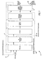
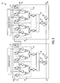
- FIG. 1 shows a high-level diagram of one preferred embodiment 10 of a specialized processing block according to the invention
- FIG. 2 is a functional diagram of the same embodiment 10.
- specialized processing block 10 includes optional input pre-MUX stage 11, optional input register stage 12, optional input multiplexing stage 13, multiplication stage 14, optional pipeline register stage 15 and adder/output stage 16.
- input pre-MUX stage 11 if provided, is to format the regular inputs, loopback inputs and cascade inputs (see below) into a form suitable for registering.
- Cascade inputs may be a one-register delayed version of a previous input, and therefore may need formatting accordingly. However, such formatting also can be done in programmable logic of the programmable logic device of which specialized processing block 10 is a part, so if formatting of cascade inputs is the only pre-MUX function required, input pre-MUX stage 11 can be omitted or, if provided, bypassed.
- the loopback input 17 may be arranged so that it is always connected to a particular multiplier or group of multipliers.
- the formatting performed by input pre-MUX stage 11 may include the direction of particular inputs to particular bit locations depending on the function to be performed by specialized processing block 10. The formatting may be carried out in one embodiment according to a stored table identifying the various possible operations (e.g., simple or complex multiplications of various sizes, shifting operations, rotation operations, etc.) and specifying the corresponding formatting required.
- input pre-MUX stage 11 may be registered by optional input register stage 12. If there in no input pre-MUX stage 11, then the input register function, if needed, can be performed in the programmable logic portion of the programmable logic device of which block 10 is a part. Therefore, input register stage 12 is considered optional. Input register stage 12, even if provided, preferably can be optionally bypassed in cases where unregistered outputs are needed or desired.
- Input multiplexing stage 13 if provided, takes registered or unregistered inputs from input pre-MUX stage 11 and inputs potentially from elsewhere in the programmable logic device and formats the data for the different operational modes. In that respect it is similar to input pre-MUX stage 11, and therefore frequently if one of input pre-MUX stage 11 and input multiplexing stage 13 is provided, the other will not be provided.
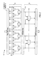
- Multiplication stage 14 preferably includes a plurality of fundamental processing units as described above.
- each specialized processing block 10 includes four fundamental processing units 30, meaning that it can perform up to eight multiplications in groups of two multiplications that are summed together.
- the fundamental processing units in specialized processing block 10 preferably are grouped into identical half-blocks, so that each half-block in its own right can be considered a specialized processing block within the invention.
- Each fundamental processing unit preferably includes the functionality for a sum of two 18-by-18 multiplications.
- the fundamental processing units preferably are all identical, but in some embodiments, it is possible to provide a negation function on only some inputs of some multipliers, as maybe required for, e.g., complex multiplication where, as is apparent above, subtraction may be required.
- the negation function may be provided in the adder portion of the fundamental processing unit, so that one or more adders can also perform subtraction.
- Each fundamental processing unit 30 preferably supports a sum of two 18-by-18 multiplications and preferably includes two partial product generators 31, two ten-vector-to-two-vector compressors 32, a 4-to-2 compressor 33, and two carry-propagate adders 34.
- Adders 34 preferably include one 30-bit adder 340 and one 24-bit adder 341, which are selectably connectable by a control signal 342. For smaller multiplications such as 9-by-9 or 12-by-12, only 24 bits are required, so the two adders can be disconnected to allow two independent multiplications. For larger multiplications such as 18-by-18, the two adders 34 should be linked as a single adder.
- Each partial product generator 31 preferably creates nine 20-bit signed Booth-encoded vectors (Booth-encoding is a known technique that can reduce the number of partial products), as well as a 17-bit unsigned carry vector (negative partial products are in ones-complement format, with the associated carry-in bit in the carry vector).
- An additional 19-bit signed partial product may be generated in the case of unsigned multipliers (which preferably will always be zero for signed multipliers).
- the carry bits preferably can be combined with the partial product vectors, requiring only 10 vectors to be compressed.
- the partial products preferably are compressed down to two 39-bit vectors (36 bits plus sign extension bits). Any sign extensions should be preserved properly past the 36-bit 18-by-18 multiplier boundary, so that any sign extensions can be valid up to the 72-bit 36-by-36 multiplier boundary (in a case where two fundamental processing units are combined to implement a 36-by-36 multiplication as described below).
- the results preferably are processed in mux-and-shift circuitry 35, which preferably include combinatorial logic where any sign-extension, zero-filling or shifting of the results before addition, as may be required depending on the operation being performed, can be accomplished prior to final combination of the results in 4-to-2 compressor 33 and carry-propagate adders 34.
- the inputs preferably are two 39-bit vectors for a total of 78 input'bits, while the outputs preferably are two 54-bit vectors for a total of 108 bits.
- the extra thirty bits are the result of sign extension, zero-filling, and or shifting.
- Multiplexer 352 indicates a selection between sign extended or zero-filled results.
- the four 54-bit vectors are input to compressor 33 which outputs two 54-bit vectors, which are added in adders 34 to produce a 54-bit output.
- the two multipliers of a fundamental processing unit cannot be used for two independent multiplications, but a single multiplication can be carried out by zeroing the inputs of the second multiplier.
- the first 9-by-9 multiplication preferably is calculated using the most significant bits (MSBs) of the first multiplier (on the left in FIG. 3), and the second 9-by-9 multiplication preferably is calculated using the least significant bits (LSBs) of the second multiplier (on the right in FIG. 3).
- MSBs of the right multiplier are filled with the sign extensions of the corresponding values, as appropriate.
- the outputs of the left multiplier (sum and carry vectors) are left-shifted by 18 bits.
- the two multiplier outputs preferably are then compressed together and the two resulting final vectors are then added with the two adders 34, which are not connected for this operation.
- the first 9-by-9 result preferably will be output on the MSBs of the left (30-bit) adder 340, while the second 9-by-9 result preferably will be output on the LSBs of the right (24-bit) adder 341.
- the right multiplier outputs are zeroed above 24 bits to prevent any interference with the independent left multiplier result.
- all inputs preferably are shifted to occupy the MSBs of the multipliers used, and the output vectors preferably are not shifted.
- the output vectors preferably are fully sign-extended, so that sign-extension out of the adders 34 can be used for the full width of the accumulator (below).
- the adder inputs can be negated (effectively making the adder an adder/subtractor).
- one or more of the multipliers can be provided with the ability to selectively negate its output vectors, by inverting the input (ones' complement), and adding the multiplicand to the result.
- the multiplicand addition can be performed in the compression of the partial products, so that the negation can be implemented before adders 34.
- Pipeline register stage 15 which preferably may be bypassed at the user's option, preferably allows outputs of multiplication stage 14 to be registered prior to further addition or accumulation or other processing.
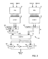
- Adder/output stage 16 preferably selectively shifts, adds, accumulates, or registers its inputs, or any combination of the above. Its inputs preferably are the outputs of the two fundamental processing units in specialized processing block 10. As seen in FIG. 4, those two inputs 40, 41 are input to respective register/shifter units 42, 43, which optionally may shift or sign extend inputs 40, 41. In a preferred embodiment, each of inputs 40, 41 is a 54-bit vector, which is shifted or sign-extended to create a respective 72-bit vector.
- the outputs of units 42, 43 preferably are input to a 3:2 compressor 44, along, preferably, with the output 45 of stage 16 itself.
- This feedback provides an accumulation function to specialized processing block 10.
- the fed-back output 45 passes through multiplexer 46, which can alternatively select a zero (e.g., ground) input when accumulation is not necessary or desired.
- the outputs of compressor 44 are provided (through appropriate multiplexers as described below) to two adders 47, 48, which may be chained together under programmable control, depending on the use to which they are to be put, as described below.
- the outputs of adders 47, 48 preferably may be registered in registers 49, 400 or not, as determined by multiplexers 401, 402. Registered or not, outputs 47, 48 preferably make up the output vector of specialized processing block 10.
- multiplexers 403, 404, 405 allow adders 47, 48 to be bypassed where the outputs of fundamental processing units 30 are to be output without further processing.
- each fundamental processing unit 30 can perform a sum of two 18-by-18 multiplications
- two fundamental processing units 30 can perform a 36-by-36 multiplication, which, as is well known, can be decomposed into four 18-by-18 multiplications.
- two compressed 72-bit vectors preferably are output by compressor 44'and preferably are added together by the two 44-bit adders 47, 48, which are programmably connected together for this mode by AND gate 406. The upper 16 bits may be ignored in this mode.
- adders 47, 48 optionally may be arranged to chain the output of specialized processing block 10 with the similar output of another specialized processing block 10.
- the output of register 400 may be fed back to 4:2 multiplexer 407, which provides two inputs to adder 47.
- the other inputs to multiplexer 407 may be the two vectors output by compressor 44 and chain-in input 408 from another specialized processing block 10, which may be provided via chain-out output 409 from register 49 of that other specialized processing block 10.
- 44-bit adder 48 may be used to add together the results within one of specialized processing blocks 10 -- configured, e.g., as a single multiplier, a sum of multipliers, or an accumulator. - with the results of the previous block.
- the output of the current specialized processing block 10 can be the chained sum of the outputs of the current and previous specialized processing blocks 10. If the chaining mode is used, only a 44-bit accumulator is available, which will still give a 6-bit to 8-bit guard band, depending on the number of multipliers. However, as is apparent, the chaining mode is not available for the 36-bit mode, in which both adders 47, 48 are needed to obtain the result of a single specialized processing block 10.
- the output paths may be slightly different depending on the mode of operation.
- multiplexers 401, 402 allow selection of registered or unregistered outputs of adders 47, 48. It will be appreciated, however, that, as shown, registered outputs preferably are used in cascade or chained mode.
- At least one output may be looped back, as at 17, to an input of specialized processing block 10.
- a loopback feature may be used, for example, if specialized processing block 10 is programmably configured for adaptive filtering.
- multiple loopbacks may be provided, in a preferred embodiment, one loopback 17 to single multiplier or group of multipliers is provided.
- the specialized processing block 10 of the present invention may be programmably configured as a long chain finite impulse response (FIR) filter.
- FIR finite impulse response
- four fundamental processing units 30 are configured as part of such a FIR filter 50.
- this may be considered to be either one or two specialized processing blocks 10.
- each of adders 48 is used to add the results of four multiplications, with adders 47 used in the chaining or cascade mode described above to add together the outputs of adders 48 (as well, possibly, as the outputs of adders 48 of other specialized processing blocks 10) to form a long FIR filter.
- the coefficients of the FIR filter are input at 51, while the data to be filtered are input via register chain 52, preferably formed in one of input pre-MUX stage 11, input register stage 12 or input multiplexing stage 13.
- register chain 52 preferably formed in one of input pre-MUX stage 11, input register stage 12 or input multiplexing stage 13.
- at least one extra delay 53 preferably is provided in input cascade chain 52.
- the number of delays corresponds to the number of adders 47 or, more particularly, output registers 409 for which delays 53 compensate. Generally, this would amount to one delay 53 for each pair of fundamental processing units 30.
- two fundamental processing units 30 make up a half-block, they also could be considered a specialized processing block 10 in their own right.
- rounding and saturation circuitry preferably also is provided in specialized processing block 10.
- the rounding circuitry preferably allows the user to select between round-to-nearest mode and round-to-nearest-even mode (truncation -- i.e., always rounding down -- also may be provided as an option).
- the saturation circuitry preferably allows the user to select between symmetrical and asymmetrical clipping.
- the rounding circuitry preferably allows the user to select which bit rounding will occur at and the saturation circuitry preferably allows the user to select which bit saturation will occur at. Insofar as those selections determine the location of the least and most significant bits, respectively, those selections allow the user to determine the width of the output word. Preferably, this is done by providing two respective four-bit variables that can be decoded into respective 16-bit numbers that represent the rounding and saturation locations, respectively.
- round-to-nearest is trivial as it involves simply adding one-half (i.e., adding 1 in the next most significant position after the rounding position) and then truncating the result (i.e., replacing all values after the rounding position with zeroes).
- round-to-nearest-even is more complicated, as it involves determining whether the value of the bits beyond the rounding position is exactly one-half or not.
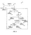
- the logic 60 for calculating the various types of rounding is shown in FIG. 6.
- RRND is the value decoded from the 4-bit number representing the rounding position
- LSB is the bit in the rounding position
- G is the next most significant bit after the rounding position (i.e., the bit to the right of the rounding position)
- S is result of ORing together all bits to the right of G.
- BIASRND 0
- RNDSEL is used, after the ORing of all RNDSEL bits as described above, as the control bit to select between rounded and unrounded values as shown, e.g., in FIGS. 7 and 8.
- the output of adder 71 is input to both rounding logic 60 and further adder 72.
- the output of rounding logic 60 is also input to adder 72, and controls whether or not adder 72 adds 1 to the output of adder 71. Because these rounding operations, as well as saturation operations in saturation logic 73, are in a critical path between registers 74, 75, the rounding and saturation operations must be completed within one clock cycle. This limits the maximum clock speed to one in which the rounding and saturation operations can be completed.
- embodiment 80 of FIG. 8 which may be programmably implemented in specialized processing block 10, instead of waiting for rounding logic 60 before performing addition 82, addition 71 and addition 82 are carried out simultaneously and the result of rounding logic 60 is used to control multiplexer 81, which selects between adders 71, 81.
- This look-ahead rounding decreases the time needed to perform rounding operations, and therefore increases the maximum permissible clock speed.
- a further embodiment 110 shown in FIG. 11, which may be programmably implemented in specialized processing block 10, is available in a round-to-nearest implementation, which, as described above, requires only adding 1 in the next most significant place and truncating. This occurs at 111 before register 74, and is therefore outside the critical path.
- Separate saturation circuitry 112 is after register 93, and therefore also is outside the critical path. While the location of saturation circuitry 112 increases Tco as in embodiment 100, it does not increase Tco by as much, because only saturation, not rounding, is being performed.
- a look-ahead implementation similar to embodiment 80 of FIG. 8 can be used in combination with the separate saturation circuitry 112 of FIG. 11.
- a specialized processing block for a programmable logic device based on a plurality of fundamental processing units, has been provided, and that such a specialized processing block can perform numerous filtering operations useful, e.g., in digital signal processing operations and similar operations.
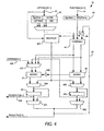
- a PLD 120 incorporating such circuitry according to the present invention may be used in many kinds of electronic devices.
- Data processing system 900 may include one or more of the following components: a processor 901; memory 902; I/O circuitry 903; and peripheral devices 904. These components are coupled together by a system bus 905 and are populated on a circuit board 906 which is contained in an end-user system 907.
- System 900 can be used in a wide variety of applications, such as computer networking, data networking, instrumentation, video processing, digital signal processing, or any other application where the advantage of using programmable or reprogrammable logic is desirable.
- PLD 120 can be used to perform a variety of different logic functions.
- PLD 120 can be configured as a processor or controller that works in cooperation with processor 901.
- PLD 120 may also be used as an arbiter for arbitrating access to a shared resources in system 900.
- PLD 120 can be configured as an interface between processor 901 and one of the other components in system 900. It should be noted that system 900 is only exemplary, and that the true scope and spirit of the invention should be indicated by the following claims.
Abstract
Description
- This claims the benefit of copending, commonly-assigned
United States Provisional Patent Application No. 60/771,989, filed February 9, 2006 - This invention relates to programmable logic devices (PLDs), and, more particularly, to specialized processing blocks which may be included in such devices.
- As applications for which PLDs are used increase in complexity, it has become more common to design PLDs to include specialized processing blocks in addition to blocks of generic programmable logic resources. Such specialized processing blocks may include a concentration of circuitry on a PLD that has been partly or fully hardwired to perform one or more specific tasks, such as a logical or a mathematical operation. A specialized processing block may also contain one or more specialized structures, such as an array of configurable memory elements. Examples of structures that are commonly implemented in such specialized processing blocks include: multipliers, arithmetic logic units (ALUs), barrel-shifters, various memory elements (such as FIFO/LIFO/SIPO/RAM/ROM/CAM blocks and register files), AND/NAND/OR/NOR arrays, etc., or combinations thereof.
- One particularly useful type of specialized processing block that has been provided on PLDs is a digital signal processing (DSP) block, which may be used to process, e.g., audio signals. Such blocks are frequently also referred to as multiply-accumulate ("MAC") blocks, because they include structures to perform multiplication operations, and sums and/or accumulations of multiplication operations.
- For example, a PLD sold by Altera Corporation, of San Jose, California, under the name STRATIX® II includes DSP blocks, each of which includes four 18-by-18 multipliers. Each of those DSP blocks also includes adders and registers, as well as programmable connectors (e.g., multiplexers) that allow the various components to be configured in different ways. In each such block, the multipliers can be configured not only as four individual 18-by-18 multipliers, but also as four smaller multipliers, or as one larger (36-by-36) multiplier. In addition, one 18-by-18 complex multiplication (which decomposes into two 18-by-18 multiplication operations for each of the real and imaginary parts) can be performed. In order to support four 18-by-18 multiplication operations, the block has 4x(18+18) = 144 inputs. Similarly, the output of an 18-by-18 multiplication is 36 bits wide, so to support the output of four such multiplication operations, the block also has 36x4 = 144 outputs.
- The operations performed by such DSP blocks frequently require rounding. However, known DSP blocks, including that provided in the aforementioned STRATIX® II PLD, have limited rounding capabilities. Similarly, DSP block operations require the ability to clip the results. Such clipping, or saturation, is necessary to prevent large positive results from overflowing to negative numbers, or highly negative results from overflowing to positive numbers. However, saturation capabilities of known DSP blocks also are limited.
- It would be desirable to be able to provide improved rounding and saturation capabilities of the DSP block of a PLD.
- The present invention relates to specialized processing blocks for PLDs wherein the specialized processing blocks have improved rounding and saturation capabilities.
- The specialized processing block with which the invention may be used preferably includes a plurality of fundamental processing units instead of discrete multipliers. Each fundamental processing unit preferably includes the equivalent of at least two multipliers and logic to sum the partial products of all of the at least two multipliers. As a result, the sums of the all of the multiplications are computed in a single step, rather than summing the.partial products of each multiplier to form individual products and then summing those products. Such a fundamental processing unit can be constructed with an area smaller than that of the individual multipliers and adders. If a single multiplication is required to be performed, one of the multipliers in the fundamental processing unit is used, while the inputs to the other(s) are zeroed out. Nevertheless, because the provision of the fundamental processing unit reduces the area of the specialized processing block, efficiency is improved.
- In a preferred embodiment, the fundamental processing unit includes the equivalent of two 18-by-28 multipliers and one adder so that it can output the sum of the two multiplication operations. While each of the 18-by-18 multipliers can be configured for a smaller multiplication operation (e.g., 9-by-9 or 12-by-12), the integrated nature of the fundamental processing unit means that the individual multiplier outputs are not accessible. Only the sum is available for use by the remainder of the specialized processing block. Therefore, to obtain the result of a single non-complex multiplication that is 18 bits-by-18 bits or smaller, an entire fundamental processing unit must be used. The second multiplier, which cannot be disengaged, simply has its inputs zeroed.
- The specialized processing block with which the invention may be used preferably also has one or more additional adders for additional processing of the output of the fundamental processing unit, as well as optional pipeline registers and a flexible output stage. Therefore the specialized processing block preferably can be configured for various forms of filtering and other digital signal processing operations. In addition, the specialized processing block preferably also has the capability to feed back at least one of its outputs as an input, which is useful in adaptive filtering operations, and to chain both inputs and outputs to additional specialized processing blocks.
- The specialized processing block according to the invention preferably includes flexible rounding circuitry and flexible saturation circuitry. The rounding and saturation circuitry preferably are in a single rounding/saturation block. However, in certain embodiments, as described below, the rounding and saturation circuitry may be separate:
- The flexible saturation circuitry according to the invention preferably allows the user to select between rounding to the nearest integer and rounding to the nearest even. As is known, rounding to the nearest even operates identically to rounding to the nearest integer, except when the remainder is exactly equal to one-half. In rounding to the nearest integer, when the remainder is exactly equal to one-half, the result always is rounded up to the next integer. In rounding to the nearest even, when the remainder is exactly equal to one-half, the result is rounded up if the next integer is even, but rounded down if the next integer is odd. The flexible rounding circuitry preferably also allows the user to select the bit position of the result at which rounding takes place. The location of the flexible rounding circuitry within the specialized processing block preferably also is selectable so that critical timing paths are not affected unnecessarily by rounding operations.
- The flexible saturation circuitry according to the invention preferably allows the user to select between symmetrical and asymmetrical clipping of the result. As is known, in certain types of numerical representations, such as one's-complement representations, a numerical variable that ranges up to 2n-1 ranges down to -(2n-1), and thus ranges symmetrically. However, in other types of numerical representations, such as two's-complement representations, a numerical variable that ranges up to 2n-1 ranges down to -(2n), and thus ranges asymmetrically. In clipping an arithmetic result, it may be desirable for the result to be clipped symmetrically regardless of the type of representation, and the present invention preferably allows the user to select such a result. The flexible saturation circuitry preferably also allows the user to select the bit position of the result at which clipping takes place. The location of the flexible saturation circuitry within the specialized processing block preferably also is selectable so that critical timing paths are not affected unnecessarily by clipping operations.
- Therefore, in accordance with the present invention, there is provided a specialized processing block for a programmable logic device. The specialized processing block includes arithmetic circuitry for providing products of inputs and sums of those products to output a result. The specialized processing block further includes one or both of (1) rounding circuitry for selectably rounding the result to one of (a) a nearest integer, and (b) a nearest even integer, and (2) saturation circuitry for clipping said result to a value inside a range of values on which said arithmetic circuitry operates.
- The above and other objects and advantages of the invention will be apparent upon consideration of the following detailed description, taken in conjunction with the accompanying drawings, in which like reference characters refer to like parts throughout, and in which:
- FIG. 1 is a high-level diagram of one preferred embodiment of a specialized processing block in accordance with the present invention;
- FIG. 2 is a functional diagram of the specialized processing block of FIG. 1;
- FIG. 3 is a block diagram of a preferred embodiment of a fundamental processing unit for a specialized processing block in accordance with the present invention;
- FIG. 4 is a preferred embodiment of an output stage of a specialized processing block in accordance with the present invention
- FIG. 5 is a functional diagram of a specialized processing block in accordance with a first preferred embodiment of the present invention configured as part of a finite impulse response filter;
- FIG. 6 is a diagram of round-to-nearest-even logic in accordance with the present invention;
- FIG. 7 is a schematic diagram of a portion of a specialized processing block showing rounding and saturation logic in accordance with a first embodiment of the present invention;
- FIG. 8 is a schematic diagram of a portion of a specialized processing block showing rounding and saturation logic in accordance with a second embodiment of the present invention;
- FIG. 9 is a schematic diagram of a portion of a specialized processing block in cascade mode showing location of rounding and saturation logic in accordance with one embodiment of the present invention;
- FIG. 10 is schematic diagram of a portion of a specialized processing block in cascade mode showing location of rounding and saturation logic in accordance with another embodiment of the present invention;
- FIG. 11 is a schematic diagram of a portion of a specialized processing block in cascade mode showing location of rounding and saturation logic in accordance with yet another embodiment of the present invention; and
- FIG. 12 is a simplified block diagram of an illustrative system employing a programmable logic device incorporating the present invention.
- Rounding is a technique for reducing the' precision of a number by removing a lower-order range of bits from that number's representation and possibly modifying the remaining portion of the number to more accurately represent its former value. For example, if the original number has N bits of precision, the rounded number may have only M bits of precision (where N>M), meaning that N-M bits of precision are removed from the number in the process of rounding.
- The round-to-nearest method returns the closest number to the original. This is commonly referred to as "round-to-nearest-integer" (RNI), but as it works for numbers less than one as well, "round-to-nearest" is more appropriate. By convention, according to this method an original number lying exactly halfway between two numbers (and therefore having two numbers that are "nearest") always rounds up to the larger of the two. For example, when rounding the 3-bit, two's complement fraction 0.25 (binary 0.01) to the nearest 2-bit two's complement fraction, this method returns 0.5 (binary 0.1). The original fraction lies exactly midway between 0.5 and 0.0 (binary 0.0), so this method rounds up. Because it always rounds up, this method is also called "biased rounding."
- The "convergent rounding," or "round-to-nearest-even" (RNE), method also returns the closest number to the original. However, in cases where the original number lies exactly halfway between two numbers, this method returns the nearest even number, which in a binary representation is the one containing a least significant bit of 0. So for the example above, the result would be 0.0, since that is the even-numbered choice as between 0.5 and 0.0. Because it rounds either up or down based on the surrounding values rather than always rounding in the same direction, this method is also called "unbiased rounding."
- Some examples are shown in the following table, in which 6-bit numbers are rounded to 4-bits of precision:
Original number (decimal equivalent) Sign First 4 bits odd or even? Last two bits </> one-half? RNI Result (decimal equivalent) RNE Result (decimal equivalent) 010111 (23) + Odd (LSB=1) Greater (.11B=.75) 011000 (24) 011000 (24) 001001 (9) + Even (LSB=0) Less (.01B=.25) 001000 (8) 001000 (8) 001010 (10) + Even (LSB=0) Equal (.10B=.50) 001100 (12) 001000 (8) 001110 (14) + Odd (LSB=1) Equal (.10B=.50) 010000 (16) 010000 (16) 110111 (-9) - Odd (LSB=1) Greater (.11B=.75) 111000 (-8) 111000 (-8) 101001 (-23) - Even (LSB=0) Less (.01B=.25) 101000 (-24) 101000 (-24) 110110 (-10) - Odd (LSB=1) Equal (.10B=.50) 111000 (-8) 111000 (-8) 110010 (-14) - Even (LSB=0) Equal (.10B=.50) 110100 (-12) 110000 (-16) - When the result of an arithmetic operation exceeds the range of the destination storage, important information can be lost. Saturation is a technique used to contain the quantity within the values that the destination storage can represent. When a value is computed that exceeds the capacity of the destination storage, then the value written to the register is "saturated at" or "clipped to" the largest value that the storage can hold with the same sign as the original.
- Thus, for example, if an operation would otherwise cause a positive value to overflow and become negative, saturation limits the result to the maximum positive value for the storage being used. Conversely, if an operation would otherwise cause a negative value to overflow and become positive, saturation limits the result to the most negative value for the storage.
- For example, if a 16-bit register containing 0x1000 (decimal integer +4096) was shifted left 3 places without saturation, it would overflow to 0x8000 (decimal -32,768). With saturation, however, a left shift of 3 or more places would always produce the largest positive 16-bit number, 0x7FFF (decimal +32,767). In the two's complement example above, where the maximum positive number is 2n-1 and the most negative number is -(2n), the saturation or clipping feature would clip the upper and lower values at 2n-1 and -(2n) if asymmetrical, but at 2n-1 and -(2n-1) if symmetrical, even though a negative value of -(2n) is available. Thus, for a 16-bit case:
- Asymmetric saturation: Max = 0x7FFF, Min = 0x8000
- Symmetric saturation: Max = 0x7FFF, Min = 0x8001
- The invention will now be described with reference to FIGS. 1-11.
- FIG. 1 shows a high-level diagram of one
preferred embodiment 10 of a specialized processing block according to the invention, while FIG. 2 is a functional diagram of thesame embodiment 10. - As seen in FIG. 1,
specialized processing block 10 includes optional inputpre-MUX stage 11, optionalinput register stage 12, optionalinput multiplexing stage 13,multiplication stage 14, optionalpipeline register stage 15 and adder/output stage 16. - The function of input
pre-MUX stage 11, if provided, is to format the regular inputs, loopback inputs and cascade inputs (see below) into a form suitable for registering. - Regular inputs do not require any specific formatting. Cascade inputs may be a one-register delayed version of a previous input, and therefore may need formatting accordingly. However, such formatting also can be done in programmable logic of the programmable logic device of which specialized processing
block 10 is a part, so if formatting of cascade inputs is the only pre-MUX function required, inputpre-MUX stage 11 can be omitted or, if provided, bypassed. Theloopback input 17 may be arranged so that it is always connected to a particular multiplier or group of multipliers. The formatting performed by inputpre-MUX stage 11 may include the direction of particular inputs to particular bit locations depending on the function to be performed byspecialized processing block 10. The formatting may be carried out in one embodiment according to a stored table identifying the various possible operations (e.g., simple or complex multiplications of various sizes, shifting operations, rotation operations, etc.) and specifying the corresponding formatting required. - The output of input
pre-MUX stage 11, if provided, may be registered by optionalinput register stage 12. If there in no inputpre-MUX stage 11, then the input register function, if needed, can be performed in the programmable logic portion of the programmable logic device of which block 10 is a part. Therefore,input register stage 12 is considered optional.Input register stage 12, even if provided, preferably can be optionally bypassed in cases where unregistered outputs are needed or desired. -
Input multiplexing stage 13, if provided, takes registered or unregistered inputs from inputpre-MUX stage 11 and inputs potentially from elsewhere in the programmable logic device and formats the data for the different operational modes. In that respect it is similar to inputpre-MUX stage 11, and therefore frequently if one of inputpre-MUX stage 11 andinput multiplexing stage 13 is provided, the other will not be provided. - As one example of the type of formatting performed by input
pre-MUX stage 11 orinput multiplexing stage 13, consider an 18-by-18 complex multiplication in which:

This complex operation requires four 18-by-18 multiplications and hence eight 18-bit inputs, but because there are only four unique 18-bit shared inputs,input multiplexing stage 13 will take the inputs a, b, c and d and perform the necessary duplication so those four inputs are properly routed to the correct multiplier inputs for each of the real and imaginary calculations. Similarly, for 9- and 12-bit mode operations, inputpre-MUX stage 11 and/orinput multiplexing stage 13 ensures correct alignments of the input bits in order to obtain correct results. -
Multiplication stage 14 preferably includes a plurality of fundamental processing units as described above. In a preferred embodiment, each specialized processing block 10 (see FIG. 2) includes fourfundamental processing units 30, meaning that it can perform up to eight multiplications in groups of two multiplications that are summed together. In that embodiment, the fundamental processing units inspecialized processing block 10 preferably are grouped into identical half-blocks, so that each half-block in its own right can be considered a specialized processing block within the invention. - Each fundamental processing unit preferably includes the functionality for a sum of two 18-by-18 multiplications. The fundamental processing units preferably are all identical, but in some embodiments, it is possible to provide a negation function on only some inputs of some multipliers, as maybe required for, e.g., complex multiplication where, as is apparent above, subtraction may be required. Alternatively, the negation function may be provided in the adder portion of the fundamental processing unit, so that one or more adders can also perform subtraction.
- The structure of a preferred embodiment of a fundamental processing unit is shown in FIG. 3. Each
fundamental processing unit 30 preferably supports a sum of two 18-by-18 multiplications and preferably includes twopartial product generators 31, two ten-vector-to-two-vector compressors 32, a 4-to-2compressor 33, and two carry-propagateadders 34.Adders 34 preferably include one 30-bit adder 340 and one 24-bit adder 341, which are selectably connectable by acontrol signal 342. For smaller multiplications such as 9-by-9 or 12-by-12, only 24 bits are required, so the two adders can be disconnected to allow two independent multiplications. For larger multiplications such as 18-by-18, the twoadders 34 should be linked as a single adder. - Each
partial product generator 31 preferably creates nine 20-bit signed Booth-encoded vectors (Booth-encoding is a known technique that can reduce the number of partial products), as well as a 17-bit unsigned carry vector (negative partial products are in ones-complement format, with the associated carry-in bit in the carry vector). An additional 19-bit signed partial product may be generated in the case of unsigned multipliers (which preferably will always be zero for signed multipliers). Although preferably up to 11 vectors may be generated, the carry bits preferably can be combined with the partial product vectors, requiring only 10 vectors to be compressed. - The partial products preferably are compressed down to two 39-bit vectors (36 bits plus sign extension bits). Any sign extensions should be preserved properly past the 36-bit 18-by-18 multiplier boundary, so that any sign extensions can be valid up to the 72-bit 36-by-36 multiplier boundary (in a case where two fundamental processing units are combined to implement a 36-by-36 multiplication as described below). After compression, the results preferably are processed in mux-and-
shift circuitry 35, which preferably include combinatorial logic where any sign-extension, zero-filling or shifting of the results before addition, as may be required depending on the operation being performed, can be accomplished prior to final combination of the results in 4-to-2compressor 33 and carry-propagateadders 34. For each ofcircuits Multiplexer 352 indicates a selection between sign extended or zero-filled results. The four 54-bit vectors are input tocompressor 33 which outputs two 54-bit vectors, which are added inadders 34 to produce a 54-bit output. - As discussed above, because the partial products from both multipliers are added at once, the two multipliers of a fundamental processing unit cannot be used for two independent multiplications, but a single multiplication can be carried out by zeroing the inputs of the second multiplier.
- For smaller multiplications, independent subset multipliers (9-by-9 and 12-by-12 cases) may be handled as follows:
- For two 9-by-9 multiplications, the first 9-by-9 multiplication preferably is calculated using the most significant bits (MSBs) of the first multiplier (on the left in FIG. 3), and the second 9-by-9 multiplication preferably is calculated using the least significant bits (LSBs) of the second multiplier (on the right in FIG. 3). The MSBs of the right multiplier are filled with the sign extensions of the corresponding values, as appropriate. The outputs of the left multiplier (sum and carry vectors) are left-shifted by 18 bits. The two multiplier outputs preferably are then compressed together and the two resulting final vectors are then added with the two
adders 34, which are not connected for this operation.
The first 9-by-9 result preferably will be output on the MSBs of the left (30-bit)adder 340, while the second 9-by-9 result preferably will be output on the LSBs of the right (24-bit)adder 341. - Independent 12-by-12 multiplications can be calculated in a manner similar to a 9-by-9 multiplication, using the MSB/LSB method.
- In both cases, preferably the right multiplier outputs are zeroed above 24 bits to prevent any interference with the independent left multiplier result.
- In the case of summed multiplications, regardless of the precision, all inputs preferably are shifted to occupy the MSBs of the multipliers used, and the output vectors preferably are not shifted. The output vectors, however, preferably are fully sign-extended, so that sign-extension out of the
adders 34 can be used for the full width of the accumulator (below). - Preferably, for complex multiplications and other operations that require subtraction of products, the adder inputs can be negated (effectively making the adder an adder/subtractor). Alternatively, however, one or more of the multipliers can be provided with the ability to selectively negate its output vectors, by inverting the input (ones' complement), and adding the multiplicand to the result. The multiplicand addition can be performed in the compression of the partial products, so that the negation can be implemented before
adders 34. -
Pipeline register stage 15, which preferably may be bypassed at the user's option, preferably allows outputs ofmultiplication stage 14 to be registered prior to further addition or accumulation or other processing. - Adder/
output stage 16 preferably selectively shifts, adds, accumulates, or registers its inputs, or any combination of the above. Its inputs preferably are the outputs of the two fundamental processing units inspecialized processing block 10. As seen in FIG. 4, those twoinputs shifter units inputs inputs - The outputs of
units compressor 44, along, preferably, with theoutput 45 ofstage 16 itself. This feedback provides an accumulation function tospecialized processing block 10. Preferably, the fed-back output 45 passes throughmultiplexer 46, which can alternatively select a zero (e.g., ground) input when accumulation is not necessary or desired. - The outputs of
compressor 44 are provided (through appropriate multiplexers as described below) to twoadders adders registers multiplexers specialized processing block 10. As an alternative path,multiplexers adders fundamental processing units 30 are to be output without further processing. - In the case, described above, where each
fundamental processing unit 30 can perform a sum of two 18-by-18 multiplications, twofundamental processing units 30 can perform a 36-by-36 multiplication, which, as is well known, can be decomposed into four 18-by-18 multiplications. In such a case, two compressed 72-bit vectors preferably are output by compressor 44'and preferably are added together by the two 44-bit adders gate 406. The upper 16 bits may be ignored in this mode. - In other modes with narrower outputs, where
adders adders specialized processing block 10 with the similar output of anotherspecialized processing block 10. To facilitate such a mode, the output ofregister 400, for example, may be fed back to 4:2multiplexer 407, which provides two inputs to adder 47. The other inputs tomultiplexer 407 may be the two vectors output bycompressor 44 and chain-ininput 408 from anotherspecialized processing block 10, which may be provided via chain-outoutput 409 fromregister 49 of that otherspecialized processing block 10. - Thus, in chaining mode, 44-
bit adder 48 may be used to add together the results within one of specialized processing blocks 10 -- configured, e.g., as a single multiplier, a sum of multipliers, or an accumulator. - with the results of the previous block. By usingmultiplexer 407 to select as inputs to adder 47 the output ofadder 48 and the output of anotherspecialized processing block 10, the output of the currentspecialized processing block 10 can be the chained sum of the outputs of the current and previous specialized processing blocks 10. If the chaining mode is used, only a 44-bit accumulator is available, which will still give a 6-bit to 8-bit guard band, depending on the number of multipliers. However, as is apparent, the chaining mode is not available for the 36-bit mode, in which bothadders specialized processing block 10. - The output paths may be slightly different depending on the mode of operation. Thus,
multiplexers adders - In addition, at least one output may be looped back, as at 17, to an input of
specialized processing block 10. Such a loopback feature may be used, for example, ifspecialized processing block 10 is programmably configured for adaptive filtering. Although multiple loopbacks may be provided, in a preferred embodiment, oneloopback 17 to single multiplier or group of multipliers is provided. - The
specialized processing block 10 of the present invention may be programmably configured as a long chain finite impulse response (FIR) filter. As shown in FIG. 5, fourfundamental processing units 30 are configured as part of such aFIR filter 50. As discussed above, this may be considered to be either one or two specialized processing blocks 10. As shown, each ofadders 48 is used to add the results of four multiplications, withadders 47 used in the chaining or cascade mode described above to add together the outputs of adders 48 (as well, possibly, as the outputs ofadders 48 of other specialized processing blocks 10) to form a long FIR filter. The coefficients of the FIR filter are input at 51, while the data to be filtered are input viaregister chain 52, preferably formed in one of inputpre-MUX stage 11,input register stage 12 orinput multiplexing stage 13. To account for delay introduced by the output cascade chain, at least one extra delay 53 (e.g., in the form of an extra register) preferably is provided ininput cascade chain 52. Preferably, the number of delays corresponds to the number ofadders 47 or, more particularly, output registers 409 for which delays 53 compensate. Generally, this would amount to onedelay 53 for each pair offundamental processing units 30. As discussed above, although in a preferred embodiment twofundamental processing units 30 make up a half-block, they also could be considered aspecialized processing block 10 in their own right. - As discussed above, rounding and saturation circuitry preferably also is provided in
specialized processing block 10. As discussed, the rounding circuitry preferably allows the user to select between round-to-nearest mode and round-to-nearest-even mode (truncation -- i.e., always rounding down -- also may be provided as an option). As also discussed, the saturation circuitry preferably allows the user to select between symmetrical and asymmetrical clipping. In addition, the rounding circuitry preferably allows the user to select which bit rounding will occur at and the saturation circuitry preferably allows the user to select which bit saturation will occur at. Insofar as those selections determine the location of the least and most significant bits, respectively, those selections allow the user to determine the width of the output word. Preferably, this is done by providing two respective four-bit variables that can be decoded into respective 16-bit numbers that represent the rounding and saturation locations, respectively. - The calculation of round-to-nearest is trivial as it involves simply adding one-half (i.e., adding 1 in the next most significant position after the rounding position) and then truncating the result (i.e., replacing all values after the rounding position with zeroes).
- The calculation of round-to-nearest-even is more complicated, as it involves determining whether the value of the bits beyond the rounding position is exactly one-half or not.
- The
logic 60 for calculating the various types of rounding is shown in FIG. 6. The variable ROUND determines ifbranch 61 orbranch 62 is followed. If ROUND = 0, no rounding is to be performed andbranch 61 is followed, setting RNDSEL = 0 at 610. If ROUND = 1, rounding is to be performed andbranch 62 is followed, and is repeated for each bit position, with the results being ORed together. Thus, in the preferred 16-bit embodiment, this is done sixteen times and ORed in a 16-bit-wide OR gate. - In
branch 62, RRND is the value decoded from the 4-bit number representing the rounding position, LSB is the bit in the rounding position, G is the next most significant bit after the rounding position (i.e., the bit to the right of the rounding position), and S is result of ORing together all bits to the right of G. Thus, for a particular pass throughbranch 62, if at 620 RRND is 0, then for that bit position there is no rounding and RNDSEL is set to 0 at 621. If at 620 RRND is 1, then for that bit position rounding is to be performed and the value of G is examined at 622. - If G = 0, then the remainder beyond LSB is less than one-half and the result should be rounded down (i.e., not rounded but truncated), and at 623 RNDSEL is set to 0. If G =1, then the remainder beyond LSB is greater than or equal to one-half, and further rounding steps depend on whether biased rounding (BIASRND = 1) or unbiased rounding (BIASRND = 0) is to be performed, as determined at 624.
- If biased rounding is to be performed (i.e., BIASRND = 1), then the result should be rounded up regardless of whether the remainder is exactly one-half, so RNDSEL is set to 1 at 625.
- If unbiased rounding is to be performed (i.e., BIASRND = 0), then the result should be rounded up only if the remainder is more than one-half, or if the remainder is exactly one-half but LSB =1. Thus, if BIASRND= 0, then at 626 the value of S is examined. If S = 1, then the remainder is more than one-half and the result should be rounded, so RNDSEL is set to 1 at 627. If S = 0, then the remainder is exactly one-half, so LSB is examined at 628. If LSB = 0, rounding to the nearest even means rounding down and RNDSEL is set to 0 at 629. If LSB = 1, rounding to the nearest even means rounding up and RNDSEL is set to 1 at 630.
- The result, RNDSEL, is used, after the ORing of all RNDSEL bits as described above, as the control bit to select between rounded and unrounded values as shown, e.g., in FIGS. 7 and 8. In the
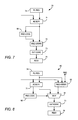
embodiment 70 of FIG. 7, which may be programmably implemented inspecialized processing block 10, the output ofadder 71 is input to both roundinglogic 60 andfurther adder 72. The output of roundinglogic 60 is also input to adder 72, and controls whether or not adder 72 adds 1 to the output ofadder 71. Because these rounding operations, as well as saturation operations insaturation logic 73, are in a critical path between registers 74, 75, the rounding and saturation operations must be completed within one clock cycle. This limits the maximum clock speed to one in which the rounding and saturation operations can be completed. - Therefore, in
embodiment 80 of FIG. 8, which may be programmably implemented inspecialized processing block 10, instead of waiting for roundinglogic 60 before performingaddition 82,addition 71 andaddition 82 are carried out simultaneously and the result of roundinglogic 60 is used to controlmultiplexer 81, which selects betweenadders - Similar clocking issues come into play when
specialized processing block 10 is used in output cascade mode with anotherspecialized processing block 10. As seen inembodiment 90 of FIG. 9, which may be programmably implemented inspecialized processing block 10, the rounding andsaturation circuitry 91 is located betweencascade adder 92 and register 93. Once again, that places it in the critical path for register timing. Therefore, in theembodiment 100 shown in FIG. 10, which may be programmably implemented inspecialized processing block 10, rounding andsaturation circuitry 91 is placed afterregister 93. While this removes rounding andsaturation circuitry 91 from the critical path, it increases the time-to-clockout (Tco), because the rounding and saturation operations are carried out later. - Therefore, a
further embodiment 110 shown in FIG. 11, which may be programmably implemented inspecialized processing block 10, is available in a round-to-nearest implementation, which, as described above, requires only adding 1 in the next most significant place and truncating. This occurs at 111 beforeregister 74, and is therefore outside the critical path.Separate saturation circuitry 112 is afterregister 93, and therefore also is outside the critical path. While the location ofsaturation circuitry 112 increases Tco as inembodiment 100, it does not increase Tco by as much, because only saturation, not rounding, is being performed. In a further alternative (not shown), a look-ahead implementation similar toembodiment 80 of FIG. 8 can be used in combination with theseparate saturation circuitry 112 of FIG. 11. - Thus it is seen that a specialized processing block for a programmable logic device, based on a plurality of fundamental processing units, has been provided, and that such a specialized processing block can perform numerous filtering operations useful, e.g., in digital signal processing operations and similar operations.
- A
PLD 120 incorporating such circuitry according to the present invention may be used in many kinds of electronic devices. One possible use is in adata processing system 900 shown in FIG. 12.Data processing system 900 may include one or more of the following components: aprocessor 901;memory 902; I/O circuitry 903; andperipheral devices 904. These components are coupled together by asystem bus 905 and are populated on acircuit board 906 which is contained in an end-user system 907. -
System 900 can be used in a wide variety of applications, such as computer networking, data networking, instrumentation, video processing, digital signal processing, or any other application where the advantage of using programmable or reprogrammable logic is desirable.PLD 120 can be used to perform a variety of different logic functions. For example,PLD 120 can be configured as a processor or controller that works in cooperation withprocessor 901.PLD 120 may also be used as an arbiter for arbitrating access to a shared resources insystem 900. In yet another example,PLD 120 can be configured as an interface betweenprocessor 901 and one of the other components insystem 900. It should be noted thatsystem 900 is only exemplary, and that the true scope and spirit of the invention should be indicated by the following claims. - Various technologies can be used to implement
PLDs 120 as described above and incorporating this invention. - It will be understood that the foregoing is only illustrative of the principles of the invention, and that various modifications can be made by those skilled in the art without departing from the scope and spirit of the invention. For example, the various elements of this invention can be provided on a PLD in any desired number and/or arrangement. One skilled in the art will appreciate that the present invention can be practiced by other than the described embodiments, which are presented for purposes of illustration and not of limitation, and the present invention is limited only by the claims that follow.
Claims (37)
- A specialized processing block for a programmable logic device, said specialized processing block comprising:arithmetic circuitry for providing products of inputs and sums of said products to output a result; androunding circuitry for selectably rounding said result to one of (a) a nearest integer, and (b) a nearest even integer.
- The specialized processing block of claim 1 wherein said rounding circuitry performs said rounding at a selectable bit position of said result.
- The specialized processing block of claim 1 wherein:said arithmetic circuitry operates on values in a range that extends up to a most highly positive value and down to a most highly negative value; said specialized processing block further comprising:saturation circuitry for clipping said result to a value inside said range.
- The specialized processing block of claim 3 wherein said saturation circuitry performs said clipping at a selectable bit position of said result.
- The specialized processing block of claim 3 wherein said saturation circuitry clips said results symmetrically.
- The specialized processing block of claim 3 wherein said saturation circuitry clips said results asymmetrically.
- The specialized processing block of claim 3 wherein said saturation circuitry operates after said rounding circuitry.
- The specialized processing block of claim 1 wherein said rounding circuitry is programmably locatable to optimize operation of said specialized processing block.
- The specialized processing block of claim 8 wherein at least a first portion of said rounding circuitry is programmably locatable in parallel with at least a portion of said arithmetic circuitry to operate in a look-ahead mode.
- The specialized processing block of claim 9 wherein:said portion of said arithmetic circuitry computes said result without rounding;said first portion of said rounding circuitry computes said result with rounding in parallel with computation by said portion of said arithmetic circuitry of said result without rounding; andsaid rounding circuitry further comprises a second portion that selects between said result with rounding and said result without rounding.
- The specialized processing block of claim 8 wherein:said arithmetic circuitry includes a register creating a critical timing path; andsaid rounding circuitry is programmably locatable in at least one position that is at least one of (a) before, and (b) after, said register so as to be programmably includable in, and excludable from, said critical timing path.
- The specialized processing block of claim 11 wherein said critical timing path includes results chained from another said specialized processing block.
- A programmable logic device comprising the specialized processing block of claim 1.
- A digital processing system comprising:processing circuitry;a memory coupled to said processing circuitry; anda programmable logic device as defined in claim 13 coupled to the processing circuitry and the memory.
- A printed circuit board on which is mounted a programmable logic device as defined in claim 13.
- The printed circuit board defined in claim 15 further comprising:memory circuitry mounted on the printed circuit board and coupled to the programmable logic device.
- The printed circuit board defined in claim 16 further comprising:processing circuitry mounted on the printed circuit board and coupled to the memory circuitry.
- An integrated circuit device comprising the specialized processing block of claim 1.
- A digital processing system comprising:processing circuitry;a memory coupled to said processing circuitry; andan integrated circuit device as defined in claim 18 coupled to the processing circuitry and the memory.
- A printed circuit board on which is mounted an integrated circuit device as defined in claim 19.
- The printed circuit board defined in claim 20 further comprising:memory circuitry mounted on the printed circuit board and coupled to the programmable logic device.
- The printed circuit board defined in claim 21 further comprising:processing circuitry mounted on the printed circuit board and coupled to the memory circuitry.
- A specialized processing block for a programmable logic device, said specialized processing block comprising:arithmetic circuitry for providing products of inputs and sums of said products to output a result; androunding circuitry for selectably rounding said result to one of (a) a nearest integer, and (b) a nearest even integer.
- The specialized processing block of claim 23 wherein:said arithmetic circuitry operates on values in a range that extends up to a most highly positive value and down to a most highly negative value; said specialized processing block further comprising:saturation circuitry for clipping said result to a value inside said range.
- The specialized processing block of claim 24 wherein said saturation circuitry performs said clipping at a selectable bit position of said result.
- The specialized processing block of claim 24 wherein said saturation circuitry clips said results symmetrically.
- The specialized processing block of claim 24 wherein said saturation circuitry clips said results asymmetrically.
- A programmable logic device comprising the specialized processing block of claim 23.
- A digital processing system comprising:processing circuitry;a memory coupled to said processing circuitry; anda programmable logic device as defined in claim 28 coupled to the processing circuitry and the memory.
- A printed circuit board on which is mounted a programmable logic device as defined in claim 28.
- The printed circuit board defined in claim 30 further comprising:memory circuitry mounted on the printed circuit board and coupled to the programmable logic device.
- The printed circuit board defined in claim 31 further comprising:processing circuitry mounted on the printed circuit board and coupled to the memory circuitry.
- An integrated circuit device comprising the specialized processing block of claim 23.
- A digital processing system comprising:processing circuitry;a memory coupled to said processing circuitry; andan integrated circuit device as defined in claim 33 coupled to the processing circuitry and the memory.
- A printed circuit board on which is mounted an integrated circuit device as defined in claim 34.
- The printed circuit board defined in claim 35 further comprising:memory circuitry mounted on the printed circuit board and coupled to the programmable logic device.
- The printed circuit board defined in claim 36 further comprising:processing circuitry mounted on the printed circuit board and coupled to the memory circuitry.
Applications Claiming Priority (2)
| Application Number | Priority Date | Filing Date | Title |
|---|---|---|---|
| US77198906P | 2006-02-09 | 2006-02-09 | |
| US11/447,329 US8266198B2 (en) | 2006-02-09 | 2006-06-05 | Specialized processing block for programmable logic device |
Publications (2)
| Publication Number | Publication Date |
|---|---|
| EP1830252A2 true EP1830252A2 (en) | 2007-09-05 |
| EP1830252A3 EP1830252A3 (en) | 2009-02-04 |
Family
ID=38110253
Family Applications (1)
| Application Number | Title | Priority Date | Filing Date |
|---|---|---|---|
| EP07002429A Withdrawn EP1830252A3 (en) | 2006-02-09 | 2007-02-05 | Specialised processing block for programmable logic device |
Country Status (4)
| Country | Link |
|---|---|
| US (1) | US8266198B2 (en) |
| EP (1) | EP1830252A3 (en) |
| JP (1) | JP5069476B2 (en) |
| CN (1) | CN101042583B (en) |
Cited By (1)
| Publication number | Priority date | Publication date | Assignee | Title |
|---|---|---|---|---|
| WO2010101985A1 (en) * | 2009-03-03 | 2010-09-10 | Altera Corporation | Digital signal processing circuitry with redundancy and bidirectional data paths |
Families Citing this family (67)
| Publication number | Priority date | Publication date | Assignee | Title |
|---|---|---|---|---|
| US8620980B1 (en) | 2005-09-27 | 2013-12-31 | Altera Corporation | Programmable device with specialized multiplier blocks |
| US8266199B2 (en) | 2006-02-09 | 2012-09-11 | Altera Corporation | Specialized processing block for programmable logic device |
| US8266198B2 (en) | 2006-02-09 | 2012-09-11 | Altera Corporation | Specialized processing block for programmable logic device |
| US8041759B1 (en) | 2006-02-09 | 2011-10-18 | Altera Corporation | Specialized processing block for programmable logic device |
| US8301681B1 (en) | 2006-02-09 | 2012-10-30 | Altera Corporation | Specialized processing block for programmable logic device |
| US7836117B1 (en) | 2006-04-07 | 2010-11-16 | Altera Corporation | Specialized processing block for programmable logic device |
| US7822799B1 (en) | 2006-06-26 | 2010-10-26 | Altera Corporation | Adder-rounder circuitry for specialized processing block in programmable logic device |
| US8386550B1 (en) | 2006-09-20 | 2013-02-26 | Altera Corporation | Method for configuring a finite impulse response filter in a programmable logic device |
| US8386553B1 (en) | 2006-12-05 | 2013-02-26 | Altera Corporation | Large multiplier for programmable logic device |
| US7930336B2 (en) | 2006-12-05 | 2011-04-19 | Altera Corporation | Large multiplier for programmable logic device |
| US8650231B1 (en) | 2007-01-22 | 2014-02-11 | Altera Corporation | Configuring floating point operations in a programmable device |
| US8645450B1 (en) | 2007-03-02 | 2014-02-04 | Altera Corporation | Multiplier-accumulator circuitry and methods |
| US7949699B1 (en) | 2007-08-30 | 2011-05-24 | Altera Corporation | Implementation of decimation filter in integrated circuit device using ram-based data storage |
| US8959137B1 (en) | 2008-02-20 | 2015-02-17 | Altera Corporation | Implementing large multipliers in a programmable integrated circuit device |
| US8244789B1 (en) | 2008-03-14 | 2012-08-14 | Altera Corporation | Normalization of floating point operations in a programmable integrated circuit device |
| WO2009118720A2 (en) * | 2008-03-25 | 2009-10-01 | Densbits Technologies Ltd. | Apparatus and methods for hardware-efficient unbiased rounding |
| US8626815B1 (en) | 2008-07-14 | 2014-01-07 | Altera Corporation | Configuring a programmable integrated circuit device to perform matrix multiplication |
| US8255448B1 (en) | 2008-10-02 | 2012-08-28 | Altera Corporation | Implementing division in a programmable integrated circuit device |
| US8307023B1 (en) | 2008-10-10 | 2012-11-06 | Altera Corporation | DSP block for implementing large multiplier on a programmable integrated circuit device |
| US8706790B1 (en) | 2009-03-03 | 2014-04-22 | Altera Corporation | Implementing mixed-precision floating-point operations in a programmable integrated circuit device |
| US8549055B2 (en) | 2009-03-03 | 2013-10-01 | Altera Corporation | Modular digital signal processing circuitry with optionally usable, dedicated connections between modules of the circuitry |
| US8645449B1 (en) | 2009-03-03 | 2014-02-04 | Altera Corporation | Combined floating point adder and subtractor |
| US8886696B1 (en) * | 2009-03-03 | 2014-11-11 | Altera Corporation | Digital signal processing circuitry with redundancy and ability to support larger multipliers |
| US8468192B1 (en) | 2009-03-03 | 2013-06-18 | Altera Corporation | Implementing multipliers in a programmable integrated circuit device |
| US8650236B1 (en) | 2009-08-04 | 2014-02-11 | Altera Corporation | High-rate interpolation or decimation filter in integrated circuit device |
| US8396914B1 (en) | 2009-09-11 | 2013-03-12 | Altera Corporation | Matrix decomposition in an integrated circuit device |
| US8412756B1 (en) | 2009-09-11 | 2013-04-02 | Altera Corporation | Multi-operand floating point operations in a programmable integrated circuit device |
| US8539016B1 (en) | 2010-02-09 | 2013-09-17 | Altera Corporation | QR decomposition in an integrated circuit device |
| US7948267B1 (en) | 2010-02-09 | 2011-05-24 | Altera Corporation | Efficient rounding circuits and methods in configurable integrated circuit devices |
| US8601044B2 (en) | 2010-03-02 | 2013-12-03 | Altera Corporation | Discrete Fourier Transform in an integrated circuit device |
| US8458243B1 (en) | 2010-03-03 | 2013-06-04 | Altera Corporation | Digital signal processing circuit blocks with support for systolic finite-impulse-response digital filtering |
| US8484265B1 (en) | 2010-03-04 | 2013-07-09 | Altera Corporation | Angular range reduction in an integrated circuit device |
| US8510354B1 (en) | 2010-03-12 | 2013-08-13 | Altera Corporation | Calculation of trigonometric functions in an integrated circuit device |
| US8539014B2 (en) | 2010-03-25 | 2013-09-17 | Altera Corporation | Solving linear matrices in an integrated circuit device |
| US8589463B2 (en) | 2010-06-25 | 2013-11-19 | Altera Corporation | Calculation of trigonometric functions in an integrated circuit device |
| US8862650B2 (en) | 2010-06-25 | 2014-10-14 | Altera Corporation | Calculation of trigonometric functions in an integrated circuit device |
| US8566376B2 (en) | 2010-07-30 | 2013-10-22 | Chevron U.S.A. Inc. | System and method for data compression using a field programmable gate array |
| US8577951B1 (en) | 2010-08-19 | 2013-11-05 | Altera Corporation | Matrix operations in an integrated circuit device |
| US8645451B2 (en) | 2011-03-10 | 2014-02-04 | Altera Corporation | Double-clocked specialized processing block in an integrated circuit device |
| US9600278B1 (en) | 2011-05-09 | 2017-03-21 | Altera Corporation | Programmable device using fixed and configurable logic to implement recursive trees |
| US8812576B1 (en) | 2011-09-12 | 2014-08-19 | Altera Corporation | QR decomposition in an integrated circuit device |
| US9053045B1 (en) | 2011-09-16 | 2015-06-09 | Altera Corporation | Computing floating-point polynomials in an integrated circuit device |
| US8949298B1 (en) | 2011-09-16 | 2015-02-03 | Altera Corporation | Computing floating-point polynomials in an integrated circuit device |
| US8762443B1 (en) | 2011-11-15 | 2014-06-24 | Altera Corporation | Matrix operations in an integrated circuit device |
| US9032277B1 (en) * | 2011-11-28 | 2015-05-12 | Altera Corporation | Parallel low and asymmetric rate Reed Solomon coding |
| US8977885B1 (en) | 2012-03-05 | 2015-03-10 | Lattice Semiconductor Corporation | Programmable logic device data rate booster for digital signal processing |
| US9143189B2 (en) * | 2012-03-30 | 2015-09-22 | Broadcom Corporation | Mobile device searching using multiple antennas |
| US8543634B1 (en) | 2012-03-30 | 2013-09-24 | Altera Corporation | Specialized processing block for programmable integrated circuit device |
| US9098332B1 (en) | 2012-06-01 | 2015-08-04 | Altera Corporation | Specialized processing block with fixed- and floating-point structures |
| US8996600B1 (en) | 2012-08-03 | 2015-03-31 | Altera Corporation | Specialized processing block for implementing floating-point multiplier with subnormal operation support |
| US9207909B1 (en) | 2012-11-26 | 2015-12-08 | Altera Corporation | Polynomial calculations optimized for programmable integrated circuit device structures |
| US9207908B1 (en) | 2013-01-29 | 2015-12-08 | Altera Corporation | Digital signal processing blocks with embedded arithmetic circuits |
| US9189200B1 (en) | 2013-03-14 | 2015-11-17 | Altera Corporation | Multiple-precision processing block in a programmable integrated circuit device |
| US9348795B1 (en) | 2013-07-03 | 2016-05-24 | Altera Corporation | Programmable device using fixed and configurable logic to implement floating-point rounding |
| US9830129B2 (en) * | 2013-11-21 | 2017-11-28 | Samsung Electronics Co., Ltd. | High performance floating-point adder with full in-line denormal/subnormal support |
| US9379687B1 (en) | 2014-01-14 | 2016-06-28 | Altera Corporation | Pipelined systolic finite impulse response filter |
| US9684488B2 (en) | 2015-03-26 | 2017-06-20 | Altera Corporation | Combined adder and pre-adder for high-radix multiplier circuit |
| US9747110B2 (en) * | 2015-05-20 | 2017-08-29 | Altera Corporation | Pipelined cascaded digital signal processing structures and methods |
| US9904514B1 (en) | 2015-10-06 | 2018-02-27 | Altera Corporation | Fused floating-point arithmetic circuitry |
| US10037192B2 (en) | 2015-10-21 | 2018-07-31 | Altera Corporation | Methods and apparatus for performing product series operations in multiplier accumulator blocks |
| US10140091B2 (en) | 2016-09-27 | 2018-11-27 | Altera Corporation | Integrated circuits with specialized processing blocks for performing floating-point fast fourier transforms and complex multiplication |
| JP6556768B2 (en) * | 2017-01-25 | 2019-08-07 | 株式会社東芝 | Multiply-accumulator, network unit and network device |
| US10579338B2 (en) * | 2017-01-30 | 2020-03-03 | Arm Limited | Apparatus and method for processing input operand values |
| US10942706B2 (en) | 2017-05-05 | 2021-03-09 | Intel Corporation | Implementation of floating-point trigonometric functions in an integrated circuit device |
| US10970042B2 (en) | 2017-11-20 | 2021-04-06 | Intel Corporation | Integrated circuits with machine learning extensions |
| US11175892B2 (en) | 2017-11-20 | 2021-11-16 | Intel Corporation | Integrated circuits with machine learning extensions |
| CN116257207B (en) * | 2022-09-08 | 2023-10-03 | 重庆位图信息技术有限公司 | Data interception method, module, computer equipment and storage medium |
Citations (1)
| Publication number | Priority date | Publication date | Assignee | Title |
|---|---|---|---|---|
| US20050187997A1 (en) | 2004-02-20 | 2005-08-25 | Leon Zheng | Flexible accumulator in digital signal processing circuitry |
Family Cites Families (343)
| Publication number | Priority date | Publication date | Assignee | Title |
|---|---|---|---|---|
| US597498A (en) * | 1898-01-18 | Boiler | ||
| US3473160A (en) | 1966-10-10 | 1969-10-14 | Stanford Research Inst | Electronically controlled microelectronic cellular logic array |
| US4215407A (en) | 1972-08-22 | 1980-07-29 | Westinghouse Electric Corp. | Combined file and directory system for a process control digital computer system |
| US4215406A (en) | 1972-08-22 | 1980-07-29 | Westinghouse Electric Corp. | Digital computer monitored and/or operated system or process which is structured for operation with an improved automatic programming process and system |
| US6556044B2 (en) * | 2001-09-18 | 2003-04-29 | Altera Corporation | Programmable logic device including multipliers and configurations thereof to reduce resource utilization |
| US3800130A (en) * | 1973-07-09 | 1974-03-26 | Rca Corp | Fast fourier transform stage using floating point numbers |
| US4179746A (en) | 1976-07-19 | 1979-12-18 | Texas Instruments Incorporated | Digital processor system with conditional carry and status function in arithmetic unit |
| US4156927A (en) * | 1976-08-11 | 1979-05-29 | Texas Instruments Incorporated | Digital processor system with direct access memory |
| US4212076A (en) | 1976-09-24 | 1980-07-08 | Giddings & Lewis, Inc. | Digital computer structure providing arithmetic and boolean logic operations, the latter controlling the former |
| US4484259A (en) | 1980-02-13 | 1984-11-20 | Intel Corporation | Fraction bus for use in a numeric data processor |
| US4422155A (en) | 1981-04-01 | 1983-12-20 | American Microsystems, Inc. | Multiplier/adder circuit |
| US4521907A (en) | 1982-05-25 | 1985-06-04 | American Microsystems, Incorporated | Multiplier/adder circuit |
| US4597053A (en) | 1983-07-01 | 1986-06-24 | Codex Corporation | Two-pass multiplier/accumulator circuit |
| US4616330A (en) | 1983-08-25 | 1986-10-07 | Honeywell Inc. | Pipelined multiply-accumulate unit |
| US4623961A (en) | 1984-03-07 | 1986-11-18 | Westinghouse Electric Corp. | Programmable controller having automatic contact line solving |
| USRE34363E (en) | 1984-03-12 | 1993-08-31 | Xilinx, Inc. | Configurable electrical circuit having configurable logic elements and configurable interconnects |
| US4575812A (en) * | 1984-05-31 | 1986-03-11 | Motorola, Inc. | X×Y Bit array multiplier/accumulator circuit |
| US4736335A (en) * | 1984-11-13 | 1988-04-05 | Zoran Corporation | Multiplier-accumulator circuit using latched sums and carries |
| US4727508A (en) * | 1984-12-14 | 1988-02-23 | Motorola, Inc. | Circuit for adding and/or subtracting numbers in logarithmic representation |
| US4682302A (en) | 1984-12-14 | 1987-07-21 | Motorola, Inc. | Logarithmic arithmetic logic unit |
| JPS61237133A (en) * | 1985-04-15 | 1986-10-22 | Nec Corp | Arithmetic circuit |
| US4718057A (en) * | 1985-08-30 | 1988-01-05 | Advanced Micro Devices, Inc. | Streamlined digital signal processor |
| US4791590A (en) | 1985-11-19 | 1988-12-13 | Cornell Research Foundation, Inc. | High performance signal processor |
| US4823295A (en) * | 1986-11-10 | 1989-04-18 | Harris Corp. | High speed signal processor |
| US4918637A (en) * | 1987-01-13 | 1990-04-17 | Hewlett-Packard Company | Multichannel decimation/interpolation filter |
| JPS63182585A (en) * | 1987-01-26 | 1988-07-27 | Toshiba Corp | Logic circuit equipped with test facilitating function |
| US4839847A (en) | 1987-04-14 | 1989-06-13 | Harris Corp. | N-clock, n-bit-serial multiplier |
| US4982354A (en) * | 1987-05-28 | 1991-01-01 | Mitsubishi Denki Kabushiki Kaisha | Digital finite impulse response filter and method |
| US5142677A (en) | 1989-05-04 | 1992-08-25 | Texas Instruments Incorporated | Context switching devices, systems and methods |
| FR2621144B1 (en) * | 1987-09-25 | 1989-12-29 | Labo Electronique Physique | MULTIPLIER PIPELINE SERIE |
| JP2639543B2 (en) * | 1987-12-02 | 1997-08-13 | 日本ビクター株式会社 | Digital filter device |
| US4871930A (en) | 1988-05-05 | 1989-10-03 | Altera Corporation | Programmable logic device with array blocks connected via programmable interconnect |
| FR2633467B1 (en) | 1988-06-24 | 1990-08-24 | Thomson Csf | FREQUENCY MULTIPLIER WITH PROGRAMMABLE MULTIPLICATION ROW |
| US5452231A (en) | 1988-10-05 | 1995-09-19 | Quickturn Design Systems, Inc. | Hierarchically connected reconfigurable logic assembly |
| JPH02155045A (en) * | 1988-12-07 | 1990-06-14 | Aputo Instr Kk | Truth value converter |
| US4912345A (en) * | 1988-12-29 | 1990-03-27 | Sgs-Thomson Microelectronics, Inc. | Programmable summing functions for programmable logic devices |
| IT1235679B (en) | 1989-01-25 | 1992-09-21 | Sgs Thomson Microelectronics | INTEGRATED PROGRAMMABLE MIXED, LOGIC AND ANALOG TYPE. |
| US5046038A (en) | 1989-07-07 | 1991-09-03 | Cyrix Corporation | Method and apparatus for performing division using a rectangular aspect ratio multiplier |
| US5255203A (en) | 1989-08-15 | 1993-10-19 | Advanced Micro Devices, Inc. | Interconnect structure for programmable logic device |
| US5128559A (en) | 1989-09-29 | 1992-07-07 | Sgs-Thomson Microelectronics, Inc. | Logic block for programmable logic devices |
| US4991010A (en) * | 1989-11-13 | 1991-02-05 | Eastman Kodak Company | Dual-mode image interpolation filter operable in a first mode for storing interpolation coefficients and in a second mode for effecting television standards conversion at a pixel rate |
| DE69130652T2 (en) | 1990-03-20 | 1999-05-06 | Fujitsu Ltd | Digital high speed parallel multiplier |
| US5267187A (en) | 1990-05-10 | 1993-11-30 | Xilinx Inc | Logic structure and circuit for fast carry |
| US5768613A (en) | 1990-07-06 | 1998-06-16 | Advanced Micro Devices, Inc. | Computing apparatus configured for partitioned processing |
| EP0466997A1 (en) | 1990-07-18 | 1992-01-22 | International Business Machines Corporation | Improved digital signal processor architecture |
| JPH04256103A (en) | 1991-02-08 | 1992-09-10 | Hitachi Ltd | Programmable controller and its programming device |
| US5122685A (en) | 1991-03-06 | 1992-06-16 | Quicklogic Corporation | Programmable application specific integrated circuit and logic cell therefor |
| JP3345894B2 (en) * | 1991-05-08 | 2002-11-18 | 日本電気株式会社 | Floating point multiplier |
| US5317209A (en) * | 1991-08-29 | 1994-05-31 | National Semiconductor Corporation | Dynamic three-state bussing capability in a configurable logic array |
| US5371422A (en) | 1991-09-03 | 1994-12-06 | Altera Corporation | Programmable logic device having multiplexers and demultiplexers randomly connected to global conductors for interconnections between logic elements |
| US5550782A (en) | 1991-09-03 | 1996-08-27 | Altera Corporation | Programmable logic array integrated circuits |
| JPH05252025A (en) | 1991-10-28 | 1993-09-28 | Texas Instr Inc <Ti> | Logic module and integrated circuit |
| JPH05134851A (en) * | 1991-11-15 | 1993-06-01 | Fujitsu Ltd | Multiplying circuit output system |
| US5208491A (en) * | 1992-01-07 | 1993-05-04 | Washington Research Foundation | Field programmable gate array |
| FR2686175B1 (en) | 1992-01-14 | 1996-12-20 | Andre Thepaut | MULTIPROCESSOR DATA PROCESSING SYSTEM. |
| JPH05216624A (en) | 1992-02-03 | 1993-08-27 | Mitsubishi Electric Corp | Arithmetic unit |
| GB9202613D0 (en) | 1992-02-07 | 1992-03-25 | Questech Ltd | Improvements in and relating to digital filters |
| US5642437A (en) * | 1992-02-22 | 1997-06-24 | Texas Instruments Incorporated | System decoder circuit with temporary bit storage and method of operation |
| US5636150A (en) | 1992-08-06 | 1997-06-03 | Sharp Kabushiki Kaisha | Data driven type digital filter unit and data driven type information processor including the same |
| US5497498A (en) | 1992-11-05 | 1996-03-05 | Giga Operations Corporation | Video processing module using a second programmable logic device which reconfigures a first programmable logic device for data transformation |
| US5357152A (en) | 1992-11-10 | 1994-10-18 | Infinite Technology Corporation | Logic system of logic networks with programmable selected functions and programmable operational controls |
| US5498975A (en) | 1992-11-19 | 1996-03-12 | Altera Corporation | Implementation of redundancy on a programmable logic device |
| EP0606653A1 (en) | 1993-01-04 | 1994-07-20 | Texas Instruments Incorporated | Field programmable distributed processing memory |
| US5339263A (en) | 1993-01-28 | 1994-08-16 | Rockwell International Corporation | Combined decimation/interpolation filter for ADC and DAC |
| US5424589A (en) | 1993-02-12 | 1995-06-13 | The Board Of Trustees Of The Leland Stanford Junior University | Electrically programmable inter-chip interconnect architecture |
| US5483178A (en) * | 1993-03-29 | 1996-01-09 | Altera Corporation | Programmable logic device with logic block outputs coupled to adjacent logic block output multiplexers |
| EP0626661A1 (en) | 1993-05-24 | 1994-11-30 | Societe D'applications Generales D'electricite Et De Mecanique Sagem | Digital image processing circuitry |
| US5528549A (en) * | 1993-05-28 | 1996-06-18 | Texas Instruments Incorporated | Apparatus, systems and methods for distributed signal processing |
| US5381357A (en) * | 1993-05-28 | 1995-01-10 | Grumman Corporation | Complex adaptive fir filter |
| US5528550A (en) | 1993-05-28 | 1996-06-18 | Texas Instruments Incorporated | Apparatus, systems and methods for implementing memory embedded search arithmetic logic unit |
| JPH06348455A (en) * | 1993-06-14 | 1994-12-22 | Matsushita Electric Ind Co Ltd | Rounding method for multiplication and multiplying circuit |
| JPH0736858A (en) | 1993-07-21 | 1995-02-07 | Hitachi Ltd | Signal processor |
| DE59408784D1 (en) * | 1993-08-09 | 1999-11-04 | Siemens Ag | Signal processing device |
| US5457644A (en) | 1993-08-20 | 1995-10-10 | Actel Corporation | Field programmable digital signal processing array integrated circuit |
| US5349250A (en) | 1993-09-02 | 1994-09-20 | Xilinx, Inc. | Logic structure and circuit for fast carry |
| US5546018A (en) | 1993-09-02 | 1996-08-13 | Xilinx, Inc. | Fast carry structure with synchronous input |
| US5740404A (en) * | 1993-09-27 | 1998-04-14 | Hitachi America Limited | Digital signal processor with on-chip select decoder and wait state generator |
| US5404324A (en) | 1993-11-01 | 1995-04-04 | Hewlett-Packard Company | Methods and apparatus for performing division and square root computations in a computer |
| US5805913A (en) | 1993-11-30 | 1998-09-08 | Texas Instruments Incorporated | Arithmetic logic unit with conditional register source selection |
| US5590350A (en) | 1993-11-30 | 1996-12-31 | Texas Instruments Incorporated | Three input arithmetic logic unit with mask generator |
| US5446651A (en) | 1993-11-30 | 1995-08-29 | Texas Instruments Incorporated | Split multiply operation |
| US5485411A (en) | 1993-11-30 | 1996-01-16 | Texas Instruments Incorporated | Three input arithmetic logic unit forming the sum of a first input anded with a first boolean combination of a second input and a third input plus a second boolean combination of the second and third inputs |
| US5640578A (en) | 1993-11-30 | 1997-06-17 | Texas Instruments Incorporated | Arithmetic logic unit having plural independent sections and register storing resultant indicator bit from every section |
| US5465224A (en) | 1993-11-30 | 1995-11-07 | Texas Instruments Incorporated | Three input arithmetic logic unit forming the sum of a first Boolean combination of first, second and third inputs plus a second Boolean combination of first, second and third inputs |
| US6098163A (en) | 1993-11-30 | 2000-08-01 | Texas Instruments Incorporated | Three input arithmetic logic unit with shifter |
| US6116768A (en) | 1993-11-30 | 2000-09-12 | Texas Instruments Incorporated | Three input arithmetic logic unit with barrel rotator |
| US5961635A (en) | 1993-11-30 | 1999-10-05 | Texas Instruments Incorporated | Three input arithmetic logic unit with barrel rotator and mask generator |
| US5596763A (en) * | 1993-11-30 | 1997-01-21 | Texas Instruments Incorporated | Three input arithmetic logic unit forming mixed arithmetic and boolean combinations |
| US5644522A (en) | 1993-11-30 | 1997-07-01 | Texas Instruments Incorporated | Method, apparatus and system for multiply rounding using redundant coded multiply result |
| US6219688B1 (en) | 1993-11-30 | 2001-04-17 | Texas Instruments Incorporated | Method, apparatus and system for sum of plural absolute differences |
| US5959871A (en) | 1993-12-23 | 1999-09-28 | Analogix/Portland State University | Programmable analog array circuit |
| US5563526A (en) | 1994-01-03 | 1996-10-08 | Texas Instruments Incorporated | Programmable mixed-mode integrated circuit architecture |
| JP3097434B2 (en) | 1994-01-25 | 2000-10-10 | ヤマハ株式会社 | Digital signal processor for adding effects |
| GB9403030D0 (en) | 1994-02-17 | 1994-04-06 | Austin Kenneth | Re-configurable application specific device |
| US5497067A (en) * | 1994-02-18 | 1996-03-05 | Shaw; Donald E. | Battery charger with timer-controlled charging, shut-off and reset operations |
| US5451948A (en) | 1994-02-28 | 1995-09-19 | Cubic Communications, Inc. | Apparatus and method for combining analog and digital automatic gain control in receivers with digital signal processing |
| US5590305A (en) * | 1994-03-28 | 1996-12-31 | Altera Corporation | Programming circuits and techniques for programming logic |
| US5563819A (en) | 1994-03-31 | 1996-10-08 | Cirrus Logic, Inc. | Fast high precision discrete-time analog finite impulse response filter |
| US5541864A (en) | 1994-04-26 | 1996-07-30 | Crystal Semiconductor | Arithmetic-free digital interpolation filter architecture |
| CN1086815C (en) * | 1994-05-04 | 2002-06-26 | 爱特梅尔股份有限公司 | Programmable logic device with regional and universal signal routing |
| US5689195A (en) | 1995-05-17 | 1997-11-18 | Altera Corporation | Programmable logic array integrated circuit devices |
| JP3365581B2 (en) | 1994-07-29 | 2003-01-14 | 富士通株式会社 | Information processing device with self-healing function |
| JPH08106375A (en) | 1994-10-03 | 1996-04-23 | Ricoh Co Ltd | Signal processing computing element |
| US5652903A (en) | 1994-11-01 | 1997-07-29 | Motorola, Inc. | DSP co-processor for use on an integrated circuit that performs multiple communication tasks |
| US5872380A (en) * | 1994-11-02 | 1999-02-16 | Lsi Logic Corporation | Hexagonal sense cell architecture |
| US5761099A (en) * | 1994-11-04 | 1998-06-02 | Altera Corporation | Programmable logic array integrated circuits with enhanced carry routing |
| US5664192A (en) | 1994-12-14 | 1997-09-02 | Motorola, Inc. | Method and system for accumulating values in a computing device |
| US5636368A (en) | 1994-12-23 | 1997-06-03 | Xilinx, Inc. | Method for programming complex PLD having more than one function block type |
| EP0721159A1 (en) | 1995-01-03 | 1996-07-10 | Texas Instruments Incorporated | Multiple-input binary adder |
| US5581199A (en) | 1995-01-04 | 1996-12-03 | Xilinx, Inc. | Interconnect architecture for field programmable gate array using variable length conductors |
| US5646875A (en) | 1995-02-27 | 1997-07-08 | International Business Machines Corporation | Denormalization system and method of operation |
| US5633601A (en) * | 1995-03-10 | 1997-05-27 | Texas Instruments Incorporated | Field programmable gate array logic module configurable as combinational or sequential circuits |
| US5572148A (en) | 1995-03-22 | 1996-11-05 | Altera Corporation | Programmable logic array integrated circuit with general-purpose memory configurable as a random access or FIFO memory |
| US5570040A (en) | 1995-03-22 | 1996-10-29 | Altera Corporation | Programmable logic array integrated circuit incorporating a first-in first-out memory |
| US5696708A (en) | 1995-03-30 | 1997-12-09 | Crystal Semiconductor | Digital filter with decimated frequency response |
| US5644519A (en) * | 1995-04-07 | 1997-07-01 | Motorola, Inc. | Method and apparatus for a multiply and accumulate circuit having a dynamic saturation range |
| US5808926A (en) * | 1995-06-01 | 1998-09-15 | Sun Microsystems, Inc. | Floating point addition methods and apparatus |
| US5771186A (en) | 1995-06-07 | 1998-06-23 | International Business Machines | System and method for multiplying in a data processing system |
| US5790446A (en) * | 1995-07-05 | 1998-08-04 | Sun Microsystems, Inc. | Floating point multiplier with reduced critical paths using delay matching techniques |
| US5570039A (en) | 1995-07-27 | 1996-10-29 | Lucent Technologies Inc. | Programmable function unit as parallel multiplier cell |
| US5559450A (en) | 1995-07-27 | 1996-09-24 | Lucent Technologies Inc. | Field programmable gate array with multi-port RAM |
| US5581501A (en) | 1995-08-17 | 1996-12-03 | Altera Corporation | Nonvolatile SRAM cells and cell arrays |
| US5761483A (en) | 1995-08-18 | 1998-06-02 | Xilinx, Inc. | Optimizing and operating a time multiplexed programmable logic device |
| US5784313A (en) | 1995-08-18 | 1998-07-21 | Xilinx, Inc. | Programmable logic device including configuration data or user data memory slices |
| US5646545A (en) | 1995-08-18 | 1997-07-08 | Xilinx, Inc. | Time multiplexed programmable logic device |
| US6072994A (en) | 1995-08-31 | 2000-06-06 | Northrop Grumman Corporation | Digitally programmable multifunction radio system architecture |
| US5859878A (en) * | 1995-08-31 | 1999-01-12 | Northrop Grumman Corporation | Common receive module for a programmable digital radio |
| US7395298B2 (en) | 1995-08-31 | 2008-07-01 | Intel Corporation | Method and apparatus for performing multiply-add operations on packed data |
| JPH0997178A (en) | 1995-09-29 | 1997-04-08 | Matsushita Electric Ind Co Ltd | Device and method for saturation operation processing |
| US5729495A (en) * | 1995-09-29 | 1998-03-17 | Altera Corporation | Dynamic nonvolatile memory cell |
| US5648732A (en) | 1995-10-04 | 1997-07-15 | Xilinx, Inc. | Field programmable pipeline array |
| US5744991A (en) * | 1995-10-16 | 1998-04-28 | Altera Corporation | System for distributing clocks using a delay lock loop in a programmable logic circuit |
| US5617058A (en) * | 1995-11-13 | 1997-04-01 | Apogee Technology, Inc. | Digital signal processing for linearization of small input signals to a tri-state power switch |
| US5894228A (en) * | 1996-01-10 | 1999-04-13 | Altera Corporation | Tristate structures for programmable logic devices |
| US6247036B1 (en) * | 1996-01-22 | 2001-06-12 | Infinite Technology Corp. | Processor with reconfigurable arithmetic data path |
| US5898602A (en) * | 1996-01-25 | 1999-04-27 | Xilinx, Inc. | Carry chain circuit with flexible carry function for implementing arithmetic and logical functions |
| US5754459A (en) * | 1996-02-08 | 1998-05-19 | Xilinx, Inc. | Multiplier circuit design for a programmable logic device |
| US5744980A (en) * | 1996-02-16 | 1998-04-28 | Actel Corporation | Flexible, high-performance static RAM architecture for field-programmable gate arrays |
| US5764555A (en) | 1996-03-13 | 1998-06-09 | International Business Machines Corporation | Method and system of rounding for division or square root: eliminating remainder calculation |
| US6005806A (en) | 1996-03-14 | 1999-12-21 | Altera Corporation | Nonvolatile configuration cells and cell arrays |
| US5777912A (en) | 1996-03-28 | 1998-07-07 | Crystal Semiconductor Corporation | Linear phase finite impulse response filter with pre-addition |
| US5869979A (en) * | 1996-04-05 | 1999-02-09 | Altera Corporation | Technique for preconditioning I/Os during reconfiguration |
| US5986465A (en) | 1996-04-09 | 1999-11-16 | Altera Corporation | Programmable logic integrated circuit architecture incorporating a global shareable expander |
| US6154049A (en) | 1998-03-27 | 2000-11-28 | Xilinx, Inc. | Multiplier fabric for use in field programmable gate arrays |
| US5949710A (en) | 1996-04-10 | 1999-09-07 | Altera Corporation | Programmable interconnect junction |
| US5784636A (en) | 1996-05-28 | 1998-07-21 | National Semiconductor Corporation | Reconfigurable computer architecture for use in signal processing applications |
| US5956265A (en) | 1996-06-07 | 1999-09-21 | Lewis; James M. | Boolean digital multiplier |
| US5825201A (en) | 1996-06-21 | 1998-10-20 | Quicklogic Corporation | Programming architecture for a programmable integrated circuit employing antifuses |
| US5880981A (en) * | 1996-08-12 | 1999-03-09 | Hitachi America, Ltd. | Method and apparatus for reducing the power consumption in a programmable digital signal processor |
| US5959891A (en) * | 1996-08-16 | 1999-09-28 | Altera Corporation | Evaluation of memory cell characteristics |
| US5838165A (en) | 1996-08-21 | 1998-11-17 | Chatter; Mukesh | High performance self modifying on-the-fly alterable logic FPGA, architecture and method |
| US6624658B2 (en) | 1999-02-04 | 2003-09-23 | Advantage Logic, Inc. | Method and apparatus for universal program controlled bus architecture |
| GB2317468B (en) | 1996-09-23 | 2001-01-24 | Advanced Risc Mach Ltd | Digital signal processing integrated circuit architecture |
| US5805477A (en) | 1996-09-26 | 1998-09-08 | Hewlett-Packard Company | Arithmetic cell for field programmable devices |
| US5825202A (en) | 1996-09-26 | 1998-10-20 | Xilinx, Inc. | Integrated circuit with field programmable and application specific logic areas |
| US5999016A (en) | 1996-10-10 | 1999-12-07 | Altera Corporation | Architectures for programmable logic devices |
| JP3790307B2 (en) | 1996-10-16 | 2006-06-28 | 株式会社ルネサステクノロジ | Data processor and data processing system |
| US5942914A (en) | 1996-10-25 | 1999-08-24 | Altera Corporation | PLD with split multiplexed inputs from global conductors |
| US5892962A (en) * | 1996-11-12 | 1999-04-06 | Lucent Technologies Inc. | FPGA-based processor |
| US6018755A (en) * | 1996-11-14 | 2000-01-25 | Altocom, Inc. | Efficient implementation of an FIR filter on a general purpose processor |
| US5812562A (en) | 1996-11-15 | 1998-09-22 | Samsung Electronics Company, Ltd. | Low cost emulation scheme implemented via clock control using JTAG controller in a scan environment |
| US6009451A (en) | 1996-11-22 | 1999-12-28 | Lucent Technologies Inc. | Method for generating barrel shifter result flags directly from input data |
| US5815422A (en) | 1997-01-24 | 1998-09-29 | Vlsi Technology, Inc. | Computer-implemented multiplication with shifting of pattern-product partials |
| US5841684A (en) | 1997-01-24 | 1998-11-24 | Vlsi Technology, Inc. | Method and apparatus for computer implemented constant multiplication with multipliers having repeated patterns including shifting of replicas and patterns having at least two digit positions with non-zero values |
| US5821776A (en) | 1997-01-31 | 1998-10-13 | Actel Corporation | Field programmable gate array with mask programmed analog function circuits |
| US5999015A (en) | 1997-02-20 | 1999-12-07 | Altera Corporation | Logic region resources for programmable logic devices |
| US5982195A (en) | 1997-02-20 | 1999-11-09 | Altera Corporation | Programmable logic device architectures |
| US5931898A (en) * | 1997-02-25 | 1999-08-03 | Lucent Technologies Inc | Finite impulse response filter |
| US5963050A (en) | 1997-02-26 | 1999-10-05 | Xilinx, Inc. | Configurable logic element with fast feedback paths |
| US5874834A (en) * | 1997-03-04 | 1999-02-23 | Xilinx, Inc. | Field programmable gate array with distributed gate-array functionality |
| US5991898A (en) | 1997-03-10 | 1999-11-23 | Mentor Graphics Corporation | Arithmetic built-in self test of multiple scan-based integrated circuits |
| US5991788A (en) | 1997-03-14 | 1999-11-23 | Xilinx, Inc. | Method for configuring an FPGA for large FFTs and other vector rotation computations |
| US5847579A (en) | 1997-03-20 | 1998-12-08 | Xilinx, Inc. | Programmable logic array with improved interconnect structure |
| US6020759A (en) * | 1997-03-21 | 2000-02-01 | Altera Corporation | Programmable logic array device with random access memory configurable as product terms |
| US6085317A (en) | 1997-08-15 | 2000-07-04 | Altera Corporation | Reconfigurable computer architecture using programmable logic devices |
| US5878250A (en) * | 1997-04-07 | 1999-03-02 | Altera Corporation | Circuitry for emulating asynchronous register loading functions |
| EP0983549B1 (en) | 1997-05-23 | 2001-12-12 | Altera Corporation (a Delaware Corporation) | Redundancy circuitry for programmable logic devices with interleaved input circuits |
| US6006321A (en) * | 1997-06-13 | 1999-12-21 | Malleable Technologies, Inc. | Programmable logic datapath that may be used in a field programmable device |
| US5970254A (en) | 1997-06-27 | 1999-10-19 | Cooke; Laurence H. | Integrated processor and programmable data path chip for reconfigurable computing |
| US5847981A (en) | 1997-09-04 | 1998-12-08 | Motorola, Inc. | Multiply and accumulate circuit |
| US5910908A (en) | 1997-09-16 | 1999-06-08 | Tektronix, Inc. | Fir filter for programmable decimation |
| JP3479438B2 (en) | 1997-09-18 | 2003-12-15 | 株式会社東芝 | Multiplication circuit |
| US6021423A (en) * | 1997-09-26 | 2000-02-01 | Xilinx, Inc. | Method for parallel-efficient configuring an FPGA for large FFTS and other vector rotation computations |
| US6020755A (en) | 1997-09-26 | 2000-02-01 | Lucent Technologies Inc. | Hybrid programmable gate arrays |
| US5944774A (en) | 1997-09-26 | 1999-08-31 | Ericsson Inc. | Methods apparatus and computer program products for accumulating logarithmic values |
| US6069487A (en) * | 1997-10-14 | 2000-05-30 | Altera Corporation | Programmable logic device circuitry for improving multiplier speed and/or efficiency |
| US6052327A (en) * | 1997-10-14 | 2000-04-18 | Altera Corporation | Dual-port programmable logic device variable depth and width memory array |
| US6157210A (en) | 1997-10-16 | 2000-12-05 | Altera Corporation | Programmable logic device with circuitry for observing programmable logic circuit signals and for preloading programmable logic circuits |
| US6107824A (en) | 1997-10-16 | 2000-08-22 | Altera Corporation | Circuitry and methods for internal interconnection of programmable logic devices |
| US6223198B1 (en) | 1998-08-14 | 2001-04-24 | Advanced Micro Devices, Inc. | Method and apparatus for multi-function arithmetic |
| US6144980A (en) | 1998-01-28 | 2000-11-07 | Advanced Micro Devices, Inc. | Method and apparatus for performing multiple types of multiplication including signed and unsigned multiplication |
| US6029187A (en) * | 1997-10-28 | 2000-02-22 | Atmel Corporation | Fast regular multiplier architecture |
| DE69835529T2 (en) | 1997-11-03 | 2007-01-18 | Harris Corp., Melbourne | RECONFIGURABLE RADIO SYSTEM CONSTRUCTION |
| US6065131A (en) * | 1997-11-26 | 2000-05-16 | International Business Machines Corporation | Multi-speed DSP kernel and clock mechanism |
| US6055555A (en) * | 1997-12-29 | 2000-04-25 | Intel Corporation | Interface for performing parallel arithmetic and round operations |
| GB9727414D0 (en) * | 1997-12-29 | 1998-02-25 | Imperial College | Logic circuit |
| US6075381A (en) | 1998-01-21 | 2000-06-13 | Micron Electronics, Inc. | Programmable logic block in an integrated circuit |
| US6405229B1 (en) * | 1998-01-29 | 2002-06-11 | Sanyo Electric Co., Ltd. | Digital filters |
| JP3291461B2 (en) | 1998-01-30 | 2002-06-10 | 三洋電機株式会社 | Digital filter |
| US6094726A (en) | 1998-02-05 | 2000-07-25 | George S. Sheng | Digital signal processor using a reconfigurable array of macrocells |
| US6097988A (en) | 1998-02-10 | 2000-08-01 | Advanced Micro Devices, Inc. | Logic system and method employing multiple configurable logic blocks and capable of implementing a state machine using a minimum amount of configurable logic |
| US6175849B1 (en) * | 1998-02-10 | 2001-01-16 | Lucent Technologies, Inc. | System for digital filtering in a fixed number of clock cycles |
| US6167415A (en) | 1998-02-10 | 2000-12-26 | Lucent Technologies, Inc. | Recursive digital filter with reset |
| US6367003B1 (en) * | 1998-03-04 | 2002-04-02 | Micron Technology, Inc. | Digital signal processor having enhanced utilization of multiply accumulate (MAC) stage and method |
| US6041339A (en) * | 1998-03-27 | 2000-03-21 | Ess Technology, Inc. | Efficient decimation filtering |
| US6377970B1 (en) * | 1998-03-31 | 2002-04-23 | Intel Corporation | Method and apparatus for computing a sum of packed data elements using SIMD multiply circuitry |
| JP3611714B2 (en) * | 1998-04-08 | 2005-01-19 | 株式会社ルネサステクノロジ | Processor |
| US5968196A (en) | 1998-04-21 | 1999-10-19 | Atmel Corporation | Configuration control in a programmable logic device using non-volatile elements |
| US6084429A (en) | 1998-04-24 | 2000-07-04 | Xilinx, Inc. | PLD having a window pane architecture with segmented and staggered interconnect wiring between logic block arrays |
| DE69817153D1 (en) * | 1998-05-08 | 2003-09-18 | St Microelectronics Srl | Digital high-speed accumulator with a large dynamic range |
| US6226735B1 (en) | 1998-05-08 | 2001-05-01 | Broadcom | Method and apparatus for configuring arbitrary sized data paths comprising multiple context processing elements |
| US6140839A (en) | 1998-05-13 | 2000-10-31 | Kaviani; Alireza S. | Computational field programmable architecture |
| US5999990A (en) | 1998-05-18 | 1999-12-07 | Motorola, Inc. | Communicator having reconfigurable resources |
| US6066960A (en) * | 1998-05-21 | 2000-05-23 | Altera Corporation | Programmable logic device having combinational logic at inputs to logic elements within logic array blocks |
| GB2342193B (en) | 1998-06-19 | 2003-06-04 | Sgs Thomson Microelectronics | Addition circuitry |
| JP2000010762A (en) | 1998-06-19 | 2000-01-14 | Mitsubishi Electric Corp | Floating-point operation device |
| US6314551B1 (en) | 1998-06-22 | 2001-11-06 | Morgan Stanley & Co. Incorporated | System processing unit extended with programmable logic for plurality of functions |
| US6467017B1 (en) | 1998-06-23 | 2002-10-15 | Altera Corporation | Programmable logic device having embedded dual-port random access memory configurable as single-port memory |
| US6163788A (en) | 1998-06-25 | 2000-12-19 | Industrial Technology Research Institute | Programmable finite impulse response processor with scalable dynamic data range |
| US6073154A (en) | 1998-06-26 | 2000-06-06 | Xilinx, Inc. | Computing multidimensional DFTs in FPGA |
| US6427157B1 (en) | 1998-07-31 | 2002-07-30 | Texas Instruments Incorporated | Fir filter structure with time- varying coefficients and filtering method for digital data scaling |
| US6487575B1 (en) | 1998-08-31 | 2002-11-26 | Advanced Micro Devices, Inc. | Early completion of iterative division |
| US6321246B1 (en) | 1998-09-16 | 2001-11-20 | Cirrus Logic, Inc. | Linear phase FIR sinc filter with multiplexing |
| US6546408B2 (en) * | 1998-09-16 | 2003-04-08 | Cirrus Logic, Inc. | Sinc filter using twisting symmetry |
| US6571268B1 (en) * | 1998-10-06 | 2003-05-27 | Texas Instruments Incorporated | Multiplier accumulator circuits |
| US7047272B2 (en) | 1998-10-06 | 2006-05-16 | Texas Instruments Incorporated | Rounding mechanisms in processors |
| EP0992885B1 (en) | 1998-10-06 | 2005-12-28 | Texas Instruments Incorporated | Multiplier accumulator circuits |
| US6421698B1 (en) | 1998-11-04 | 2002-07-16 | Teleman Multimedia, Inc. | Multipurpose processor for motion estimation, pixel processing, and general processing |
| US6453382B1 (en) | 1998-11-05 | 2002-09-17 | Altera Corporation | Content addressable memory encoded outputs |
| US6091261A (en) | 1998-11-12 | 2000-07-18 | Sun Microsystems, Inc. | Apparatus and method for programmable delays using a boundary-scan chain |
| US6215326B1 (en) * | 1998-11-18 | 2001-04-10 | Altera Corporation | Programmable logic device architecture with super-regions having logic regions and a memory region |
| US6260053B1 (en) | 1998-12-09 | 2001-07-10 | Cirrus Logic, Inc. | Efficient and scalable FIR filter architecture for decimation |
| US6591283B1 (en) | 1998-12-24 | 2003-07-08 | Stmicroelectronics N.V. | Efficient interpolator for high speed timing recovery |
| US6243729B1 (en) | 1998-12-31 | 2001-06-05 | Texas Instruments Incorporated | Digital finite-impulse-response (FIR) filter with a modified architecture based on high order Radix-N numbering |
| US6366944B1 (en) * | 1999-01-15 | 2002-04-02 | Razak Hossain | Method and apparatus for performing signed/unsigned multiplication |
| US6523055B1 (en) * | 1999-01-20 | 2003-02-18 | Lsi Logic Corporation | Circuit and method for multiplying and accumulating the sum of two products in a single cycle |
| US6107821A (en) | 1999-02-08 | 2000-08-22 | Xilinx, Inc. | On-chip logic analysis and method for using the same |
| US6823000B1 (en) | 1999-02-26 | 2004-11-23 | Texas Instruments Incorporated | Method and apparatus for optimal dot product calculation |
| US6407576B1 (en) | 1999-03-04 | 2002-06-18 | Altera Corporation | Interconnection and input/output resources for programmable logic integrated circuit devices |
| JP2002538562A (en) * | 1999-03-04 | 2002-11-12 | アルテラ・コーポレーション | Programmable logic device with carry selection and addition |
| US6323680B1 (en) | 1999-03-04 | 2001-11-27 | Altera Corporation | Programmable logic device configured to accommodate multiplication |
| JP2000259394A (en) | 1999-03-09 | 2000-09-22 | Nec Kofu Ltd | Floating point multiplier |
| US6480980B2 (en) | 1999-03-10 | 2002-11-12 | Nec Electronics, Inc. | Combinational test pattern generation method and apparatus |
| US6557092B1 (en) * | 1999-03-29 | 2003-04-29 | Greg S. Callen | Programmable ALU |
| WO2000058857A2 (en) | 1999-03-30 | 2000-10-05 | Siemens Energy & Automation, Inc. | Programmable logic controller method, system and apparatus |
| US6363650B1 (en) * | 1999-04-07 | 2002-04-02 | Clinton R. Beeler | Fishing rod holder and jigging assembly |
| EP1058185A1 (en) * | 1999-05-31 | 2000-12-06 | Motorola, Inc. | A multiply and accumulate apparatus and a method thereof |
| US6434587B1 (en) | 1999-06-14 | 2002-08-13 | Intel Corporation | Fast 16-B early termination implementation for 32-B multiply-accumulate unit |
| US6246258B1 (en) | 1999-06-21 | 2001-06-12 | Xilinx, Inc. | Realizing analog-to-digital converter on a digital programmable integrated circuit |
| US6438570B1 (en) | 1999-07-21 | 2002-08-20 | Xilinx, Inc. | FPGA implemented bit-serial multiplier and infinite impulse response |
| US6542000B1 (en) * | 1999-07-30 | 2003-04-01 | Iowa State University Research Foundation, Inc. | Nonvolatile programmable logic devices |
| US6801924B1 (en) | 1999-08-19 | 2004-10-05 | National Semiconductor Corporation | Formatting denormal numbers for processing in a pipelined floating point unit |
| US6692534B1 (en) * | 1999-09-08 | 2004-02-17 | Sun Microsystems, Inc. | Specialized booth decoding apparatus |
| US6600788B1 (en) | 1999-09-10 | 2003-07-29 | Xilinx, Inc. | Narrow-band filter including sigma-delta modulator implemented in a programmable logic device |
| US6438569B1 (en) | 1999-09-20 | 2002-08-20 | Pmc-Sierra, Inc. | Sums of production datapath |
| US6353843B1 (en) * | 1999-10-08 | 2002-03-05 | Sony Corporation Of Japan | High performance universal multiplier circuit |
| AU3082701A (en) | 1999-12-23 | 2001-07-03 | Intel Corporation | Method and apparatus for performing single-cycle addition or subtraction and comparison in redundant form arithmetic |
| US6600495B1 (en) | 2000-01-10 | 2003-07-29 | Koninklijke Philips Electronics N.V. | Image interpolation and decimation using a continuously variable delay filter and combined with a polyphase filter |
| US7062526B1 (en) | 2000-02-18 | 2006-06-13 | Texas Instruments Incorporated | Microprocessor with rounding multiply instructions |
| US6687722B1 (en) * | 2000-03-16 | 2004-02-03 | Agere Systems, Inc. | High-speed/low power finite impulse response filter |
| US6725441B1 (en) * | 2000-03-22 | 2004-04-20 | Xilinx, Inc. | Method and apparatus for defining and modifying connections between logic cores implemented on programmable logic devices |
| US6574762B1 (en) | 2000-03-31 | 2003-06-03 | Lsi Logic Corporation | Use of a scan chain for configuration of BIST unit operation |
| US6362650B1 (en) | 2000-05-18 | 2002-03-26 | Xilinx, Inc. | Method and apparatus for incorporating a multiplier into an FPGA |
| US6407694B1 (en) | 2000-06-14 | 2002-06-18 | Raytheon Company | General purpose filter |
| GB2363924A (en) * | 2000-06-20 | 2002-01-09 | Virata Ltd | Processor for FIR filtering |
| DE60015119D1 (en) * | 2000-08-01 | 2004-11-25 | St Microelectronics Sa | Saturation in an arithmetic unit |
| US6476636B1 (en) | 2000-09-02 | 2002-11-05 | Actel Corporation | Tileable field-programmable gate array architecture |
| US6732134B1 (en) | 2000-09-11 | 2004-05-04 | Apple Computer, Inc. | Handler for floating-point denormalized numbers |
| US6538470B1 (en) | 2000-09-18 | 2003-03-25 | Altera Corporation | Devices and methods with programmable logic and digital signal processing regions |
| US6628140B2 (en) | 2000-09-18 | 2003-09-30 | Altera Corporation | Programmable logic devices with function-specific blocks |
| JP2002108606A (en) | 2000-09-26 | 2002-04-12 | Toshiba Corp | Sticky bit generating circuit and multiplier |
| JP2004512716A (en) | 2000-10-02 | 2004-04-22 | アルテラ・コーポレイション | Programmable logic integrated circuit device including dedicated processor device |
| US20020049798A1 (en) * | 2000-10-24 | 2002-04-25 | Minsheng Wang | Adder-saving implementation of digital interpolation/decimation fir filter |
| EP1220108A3 (en) | 2000-10-26 | 2005-01-12 | Cypress Semiconductor Corporation | Programmable circuit |
| US6763367B2 (en) | 2000-12-11 | 2004-07-13 | International Business Machines Corporation | Pre-reduction technique within a multiplier/accumulator architecture |
| US6427158B1 (en) | 2000-12-14 | 2002-07-30 | Texas Instruments Incorporated | FIR decimation filter and method |
| US6742012B2 (en) | 2000-12-27 | 2004-05-25 | Arm Limited | Apparatus and method for performing multiplication operations |
| US6483343B1 (en) | 2000-12-29 | 2002-11-19 | Quicklogic Corporation | Configurable computational unit embedded in a programmable device |
| US7020673B2 (en) * | 2001-01-19 | 2006-03-28 | Sony Corporation | Reconfigurable arithmetic device and arithmetic system including that arithmetic device and address generation device and interleave device applicable to arithmetic system |
| US7181484B2 (en) * | 2001-02-21 | 2007-02-20 | Mips Technologies, Inc. | Extended-precision accumulation of multiplier output |
| JP3492638B2 (en) | 2001-02-23 | 2004-02-03 | エヌイーシーコンピュータテクノ株式会社 | Floating point multiplier |
| US6836839B2 (en) | 2001-03-22 | 2004-12-28 | Quicksilver Technology, Inc. | Adaptive integrated circuitry with heterogeneous and reconfigurable matrices of diverse and adaptive computational units having fixed, application specific computational elements |
| US6978287B1 (en) * | 2001-04-04 | 2005-12-20 | Altera Corporation | DSP processor architecture with write datapath word conditioning and analysis |
| US20030088757A1 (en) | 2001-05-02 | 2003-05-08 | Joshua Lindner | Efficient high performance data operation element for use in a reconfigurable logic environment |
| US6963890B2 (en) | 2001-05-31 | 2005-11-08 | Koninklijke Philips Electronics N.V. | Reconfigurable digital filter having multiple filtering modes |
| US6889238B2 (en) | 2001-06-25 | 2005-05-03 | Lockheed Martin Corporation | Parallel decimator adaptive filter and method for all-rate gigabit-per-second modems |
| EP1271782B1 (en) | 2001-06-29 | 2005-05-18 | STMicroelectronics Pvt. Ltd | FPGA with at least two different and independently configurable memory structures |
| US6874079B2 (en) * | 2001-07-25 | 2005-03-29 | Quicksilver Technology | Adaptive computing engine with dataflow graph based sequencing in reconfigurable mini-matrices of composite functional blocks |
| US7107305B2 (en) | 2001-10-05 | 2006-09-12 | Intel Corporation | Multiply-accumulate (MAC) unit for single-instruction/multiple-data (SIMD) instructions |
| US7430578B2 (en) | 2001-10-29 | 2008-09-30 | Intel Corporation | Method and apparatus for performing multiply-add operations on packed byte data |
| US6924663B2 (en) | 2001-12-28 | 2005-08-02 | Fujitsu Limited | Programmable logic device with ferroelectric configuration memories |
| US6700581B2 (en) * | 2002-03-01 | 2004-03-02 | 3D Labs Inc., Ltd. | In-circuit test using scan chains |
| US7200735B2 (en) | 2002-04-10 | 2007-04-03 | Tensilica, Inc. | High-performance hybrid processor with configurable execution units |
| GB0208329D0 (en) | 2002-04-11 | 2002-05-22 | Univ York | Data processing particularly in communication systems |
| US6781408B1 (en) | 2002-04-24 | 2004-08-24 | Altera Corporation | Programmable logic device with routing channels |
| US7461115B2 (en) * | 2002-05-01 | 2008-12-02 | Sun Microsystems, Inc. | Modular multiplier |
| US6970012B2 (en) | 2002-06-10 | 2005-11-29 | Xilinx, Inc. | Programmable logic device having heterogeneous programmable logic blocks |
| US7447310B2 (en) | 2002-08-06 | 2008-11-04 | The State Of Oregon Acting By And Through The State Board Of Higher Education On Behalf Of Oregon State University | Lean multiplication of multi-precision numbers over GF(2m) |
| US7401109B2 (en) | 2002-08-06 | 2008-07-15 | The State Of Oregon Acting By And Through The State Board Of Higher Education On Behalf Of Oregon State University | Multiplication of multi-precision numbers having a size of a power of two |
| US7464310B2 (en) * | 2002-09-30 | 2008-12-09 | Broadcom Corporation | Programmable state machine of an integrated circuit |
| US7103814B2 (en) * | 2002-10-25 | 2006-09-05 | International Business Machines Corporation | Testing logic and embedded memory in parallel |
| FI118612B (en) | 2002-11-06 | 2008-01-15 | Nokia Corp | Method and system for performing landing operations and apparatus |
| FI118654B (en) | 2002-11-06 | 2008-01-31 | Nokia Corp | Method and system for performing landing operations and apparatus |
| US6971083B1 (en) | 2002-11-13 | 2005-11-29 | Altera Corporation | Method for programming programmable logic device with blocks that perform multiplication and other arithmetic functions |
| US20040103133A1 (en) | 2002-11-27 | 2004-05-27 | Spectrum Signal Processing Inc. | Decimating filter |
| US20040172439A1 (en) | 2002-12-06 | 2004-09-02 | The Research Foundation Of State University Of New York | Unified multiplier triple-expansion scheme and extra regular compact low-power implementations with borrow parallel counter circuits |
| US6774669B1 (en) | 2002-12-30 | 2004-08-10 | Actel Corporation | Field programmable gate array freeway architecture |
| US7430656B2 (en) | 2002-12-31 | 2008-09-30 | Intel Corporation | System and method of converting data formats and communicating between execution units |
| US7975197B2 (en) | 2003-03-31 | 2011-07-05 | Lsi Corporation | On-chip scan clock generator for ASIC testing |
| US7093204B2 (en) | 2003-04-04 | 2006-08-15 | Synplicity, Inc. | Method and apparatus for automated synthesis of multi-channel circuits |
| US7689641B2 (en) | 2003-06-30 | 2010-03-30 | Intel Corporation | SIMD integer multiply high with round and shift |
| JP3853766B2 (en) | 2003-07-25 | 2006-12-06 | ローム株式会社 | Logic operation circuit and logic operation device |
| US7313585B2 (en) | 2003-08-30 | 2007-12-25 | Hewlett-Packard Development Company, L.P. | Multiplier circuit |
| US7084923B2 (en) * | 2003-10-28 | 2006-08-01 | Clairvoyante, Inc | Display system having improved multiple modes for displaying image data from multiple input source formats |
| EP1700231B1 (en) * | 2003-12-29 | 2012-10-17 | Xilinx, Inc. | Integrated circuit with cascading dsp slices |
| US7567997B2 (en) | 2003-12-29 | 2009-07-28 | Xilinx, Inc. | Applications of cascading DSP slices |
| US7480690B2 (en) | 2003-12-29 | 2009-01-20 | Xilinx, Inc. | Arithmetic circuit with multiplexed addend inputs |
| US7472155B2 (en) | 2003-12-29 | 2008-12-30 | Xilinx, Inc. | Programmable logic device with cascading DSP slices |
| JP4332036B2 (en) | 2004-01-08 | 2009-09-16 | 新日本製鐵株式会社 | Steel plate corner breakage detection apparatus and corner breakage detection method |
| US7769797B2 (en) | 2004-01-20 | 2010-08-03 | Samsung Electronics Co., Ltd. | Apparatus and method of multiplication using a plurality of identical partial multiplication modules |
| US7467176B2 (en) | 2004-02-20 | 2008-12-16 | Altera Corporation | Saturation and rounding in multiply-accumulate blocks |
| DE102004009048A1 (en) | 2004-02-23 | 2005-09-08 | Schunk Ultraschalltechnik Gmbh | Tool |
| US7797363B2 (en) * | 2004-04-07 | 2010-09-14 | Sandbridge Technologies, Inc. | Processor having parallel vector multiply and reduce operations with sequential semantics |
| JP4554431B2 (en) | 2004-05-18 | 2010-09-29 | ローム株式会社 | DTMF signal generation circuit, sound signal generation circuit, and communication apparatus |
| US7409417B2 (en) | 2004-05-24 | 2008-08-05 | Broadcom Corporation | Polyphase filter with optimized silicon area |
| US7415542B2 (en) | 2004-06-18 | 2008-08-19 | Analog Devices, Inc. | Micro-programmable filter engine having plurality of filter elements interconnected in chain configuration wherein engine supports multiple filters from filter elements |
| US20060020655A1 (en) * | 2004-06-29 | 2006-01-26 | The Research Foundation Of State University Of New York | Library of low-cost low-power and high-performance multipliers |
| US7421465B1 (en) | 2004-06-30 | 2008-09-02 | Sun Microsystems, Inc. | Arithmetic early bypass |
| US7428566B2 (en) | 2004-11-10 | 2008-09-23 | Nvidia Corporation | Multipurpose functional unit with multiply-add and format conversion pipeline |
| US7668896B2 (en) * | 2004-11-30 | 2010-02-23 | Arm Limited | Data processing apparatus and method for performing floating point multiplication |
| US7298169B2 (en) | 2005-03-15 | 2007-11-20 | Tabula, Inc | Hybrid logic/interconnect circuit in a configurable IC |
| US20070083585A1 (en) * | 2005-07-25 | 2007-04-12 | Elliptic Semiconductor Inc. | Karatsuba based multiplier and method |
| US7590676B1 (en) | 2005-09-27 | 2009-09-15 | Altera Corporation | Programmable logic device with specialized multiplier blocks |
| JP4982080B2 (en) | 2005-12-16 | 2012-07-25 | パナソニック株式会社 | Digital filter |
| US8266199B2 (en) | 2006-02-09 | 2012-09-11 | Altera Corporation | Specialized processing block for programmable logic device |
| US8266198B2 (en) | 2006-02-09 | 2012-09-11 | Altera Corporation | Specialized processing block for programmable logic device |
| US7822799B1 (en) | 2006-06-26 | 2010-10-26 | Altera Corporation | Adder-rounder circuitry for specialized processing block in programmable logic device |
| US7930336B2 (en) * | 2006-12-05 | 2011-04-19 | Altera Corporation | Large multiplier for programmable logic device |
| US8090756B2 (en) | 2007-01-29 | 2012-01-03 | International Business Machines Corporation | Method and apparatus for generating trigonometric results |
| DE112008003098B4 (en) | 2007-11-16 | 2023-12-28 | Teradyne, Inc. | Method and device for calculating interpolation factors in sampling rate conversion systems |
| US8166090B2 (en) | 2007-12-28 | 2012-04-24 | L3 Communications Integrated Systems, L.P. | Tiled architecture for stationary-method iterative linear solvers |
| JP4883190B2 (en) * | 2008-01-22 | 2012-02-22 | 日本電気株式会社 | Radio access system transmitter and receiver, radio access system transmission method and reception method, and program |
| US8200728B2 (en) | 2008-05-29 | 2012-06-12 | Harris Corporation | Sine/cosine generator |
-
2006
- 2006-06-05 US US11/447,329 patent/US8266198B2/en active Active
-
2007
- 2007-02-05 EP EP07002429A patent/EP1830252A3/en not_active Withdrawn
- 2007-02-08 CN CN200710087956XA patent/CN101042583B/en active Active
- 2007-02-08 JP JP2007029842A patent/JP5069476B2/en not_active Expired - Fee Related
Patent Citations (1)
| Publication number | Priority date | Publication date | Assignee | Title |
|---|---|---|---|---|
| US20050187997A1 (en) | 2004-02-20 | 2005-08-25 | Leon Zheng | Flexible accumulator in digital signal processing circuitry |
Cited By (2)
| Publication number | Priority date | Publication date | Assignee | Title |
|---|---|---|---|---|
| WO2010101985A1 (en) * | 2009-03-03 | 2010-09-10 | Altera Corporation | Digital signal processing circuitry with redundancy and bidirectional data paths |
| WO2010102007A3 (en) * | 2009-03-03 | 2010-11-25 | Altera Corporation | Modular digital signal processing circuitry with optionally usable, dedicated connections between modules of the circuitry |
Also Published As
| Publication number | Publication date |
|---|---|
| US8266198B2 (en) | 2012-09-11 |
| JP2007215192A (en) | 2007-08-23 |
| CN101042583A (en) | 2007-09-26 |
| CN101042583B (en) | 2011-03-02 |
| EP1830252A3 (en) | 2009-02-04 |
| US20070185951A1 (en) | 2007-08-09 |
| JP5069476B2 (en) | 2012-11-07 |
Similar Documents
| Publication | Publication Date | Title |
|---|---|---|
| US8266198B2 (en) | Specialized processing block for programmable logic device | |
| US7822799B1 (en) | Adder-rounder circuitry for specialized processing block in programmable logic device | |
| EP1819049B1 (en) | Specialized processing block for programmable logic device | |
| US8301681B1 (en) | Specialized processing block for programmable logic device | |
| US10838695B2 (en) | Fixed-point and floating-point arithmetic operator circuits in specialized processing blocks | |
| US10761805B2 (en) | Reduced floating-point precision arithmetic circuitry | |
| US8041759B1 (en) | Specialized processing block for programmable logic device | |
| US7836117B1 (en) | Specialized processing block for programmable logic device | |
| CN114402289B (en) | Multi-mode arithmetic circuit | |
| US9098332B1 (en) | Specialized processing block with fixed- and floating-point structures | |
| US9552190B1 (en) | Fused floating point datapath with correct rounding | |
| EP2523095A2 (en) | DSP block with embedded floating point structures | |
| US7948267B1 (en) | Efficient rounding circuits and methods in configurable integrated circuit devices | |
| US8996600B1 (en) | Specialized processing block for implementing floating-point multiplier with subnormal operation support | |
| US10037189B2 (en) | Distributed double-precision floating-point multiplication | |
| US10127013B1 (en) | Specialized processing blocks with fixed-point and floating-point structures | |
| EP3073369A1 (en) | Combined adder and pre-adder for high-radix multiplier circuit |
Legal Events
| Date | Code | Title | Description |
|---|---|---|---|
| PUAI | Public reference made under article 153(3) epc to a published international application that has entered the european phase |
Free format text: ORIGINAL CODE: 0009012 |
|
| AK | Designated contracting states |
Kind code of ref document: A2 Designated state(s): AT BE BG CH CY CZ DE DK EE ES FI FR GB GR HU IE IS IT LI LT LU LV MC NL PL PT RO SE SI SK TR |
|
| AX | Request for extension of the european patent |
Extension state: AL BA HR MK YU |
|
| PUAL | Search report despatched |
Free format text: ORIGINAL CODE: 0009013 |
|
| AK | Designated contracting states |
Kind code of ref document: A3 Designated state(s): AT BE BG CH CY CZ DE DK EE ES FI FR GB GR HU IE IS IT LI LT LU LV MC NL PL PT RO SE SI SK TR |
|
| AX | Request for extension of the european patent |
Extension state: AL BA HR MK RS |
|
| 17P | Request for examination filed |
Effective date: 20090803 |
|
| AKX | Designation fees paid |
Designated state(s): DE GB |
|
| 17Q | First examination report despatched |
Effective date: 20100727 |
|
| STAA | Information on the status of an ep patent application or granted ep patent |
Free format text: STATUS: THE APPLICATION HAS BEEN WITHDRAWN |
|
| 18W | Application withdrawn |
Effective date: 20121109 |