EP1857873A2 - Camera illumination unit - Google Patents
Camera illumination unit Download PDFInfo
- Publication number
- EP1857873A2 EP1857873A2 EP07008730A EP07008730A EP1857873A2 EP 1857873 A2 EP1857873 A2 EP 1857873A2 EP 07008730 A EP07008730 A EP 07008730A EP 07008730 A EP07008730 A EP 07008730A EP 1857873 A2 EP1857873 A2 EP 1857873A2
- Authority
- EP
- European Patent Office
- Prior art keywords
- functional element
- optical functional
- optoelectronic sensor
- sensor according
- light
- Prior art date
- Legal status (The legal status is an assumption and is not a legal conclusion. Google has not performed a legal analysis and makes no representation as to the accuracy of the status listed.)
- Withdrawn
Links
Images
Classifications
-
- G—PHYSICS
- G03—PHOTOGRAPHY; CINEMATOGRAPHY; ANALOGOUS TECHNIQUES USING WAVES OTHER THAN OPTICAL WAVES; ELECTROGRAPHY; HOLOGRAPHY
- G03B—APPARATUS OR ARRANGEMENTS FOR TAKING PHOTOGRAPHS OR FOR PROJECTING OR VIEWING THEM; APPARATUS OR ARRANGEMENTS EMPLOYING ANALOGOUS TECHNIQUES USING WAVES OTHER THAN OPTICAL WAVES; ACCESSORIES THEREFOR
- G03B15/00—Special procedures for taking photographs; Apparatus therefor
- G03B15/02—Illuminating scene
- G03B15/03—Combinations of cameras with lighting apparatus; Flash units
-
- H—ELECTRICITY
- H04—ELECTRIC COMMUNICATION TECHNIQUE
- H04N—PICTORIAL COMMUNICATION, e.g. TELEVISION
- H04N23/00—Cameras or camera modules comprising electronic image sensors; Control thereof
- H04N23/56—Cameras or camera modules comprising electronic image sensors; Control thereof provided with illuminating means
Definitions
- the invention relates to an optoelectronic sensor for non-contact detection of objects according to the preamble of claim 1.
- Such sensors are used, for example, in a manufacturing process to detect the presence of an object within a range can. This recognition is often associated with other functions such as a positionally accurate position detection, a sorting or selection function, etc.
- the object is illuminated with a lighting device, thereby detecting the object reflected or remitted light with a recording system.
- the recording system consists of a receiving objective and a light receiving unit arranged in its image plane.
- the light receiving unit consists of one or more photosensitive elements.
- such a recording system may consist of a simple light barrier with, for example, a single position-sensitive light-receiving unit or a digital camera.
- the light receiving unit is usually a matrix arrangement of a plurality of photosensitive elements, which are constructed in CMOS or CCD technology.
- a suitable evaluation system for image processing is usually connected downstream.
- the lighting devices known from the prior art are, for example, equipped with incandescent lamps, LEDs or lamps equipped with laser sources, the light of which is also partially directed to the objects with conventional lenses or glass fibers.
- light is not limited to the visible light. Under “light” are generally electromagnetic radiation, ie UV light, IR light and visible light to understand, which can usually be used for the operation of optoelectronic sensors.
- Such known in the art optoelectronic sensors often have problems in the application, when objects whose surface has a high gloss ratio to be reliably detected.
- the problems are due to the fact that when a high gloss object on the surface is illuminated with a directional light beam, the reflected light can be reflected by the gloss level of the object in a direction that is outside the aperture of the receiving lens.
- the image contents, which are assigned to the gloss component of the object are dark on the light receiving unit and thus can not be evaluated or only conditionally evaluated.
- the resulting hot spots reduce the image quality such that the detection performance of the optoelectronic sensor is greatly reduced.
- a dome lighting In a dome lighting, the object to be illuminated is enclosed by a nearly hemispherical hood. This hemispherical hood is covered on its inner surface with a diffusely reflecting surface layer.
- a plurality of wide-scattering light sources are arranged, which in particular illuminate the inner wall of the hemispherical hood and thus also the object. In this way, the object is illuminated from a large solid angle range out.
- This, for the illumination of the object itself good dome illumination brings in practical use several disadvantages. So in particular the large height of Disadvantage that severely limits the space between the sensor and the object plane.
- Another disadvantage of this dome lighting is to be seen in that such a large lighting device can no longer be meaningfully integrated with the recording system to form a unit.
- the invention is therefore based on the object, with a flat as possible lighting device that is inherently connected to the recording system, a object located in the object level allows diffuse lighting from a large solid angle range out.
- an optoelectronic sensor for non-contact detection of objects or object features which has a recording system with a receiving lens and a light receiving unit.
- an incident light illumination device is inherently connected to the recording system in this sensor, with which the object plane is illuminated.
- the inherent incident illumination device in its outer shape has substantially the shape of a flat disc which surrounds the receiving lens rotationally symmetrical.
- the epi-illumination device has a central opening through which the light reflected from the object can enter the receiving objective.
- the receiving system and incident light illumination device form a compact unit in which the required electrical supply and data lines of the two components are combined in an advantageous manner.
- an optical functional element adapted to the size of the outer shape is coupled in whose boundary surface, which faces away from the object, several light sources to emit their emitted light and the light emerges uniformly distributed from the boundary surface facing the object Object level illuminated with homogeneous luminous intensity distribution. It is particularly advantageous if the outer diameter of the optical functional element is often greater than the effective aperture diameter of the receiving lens, because thereby also the surface portions of an object, which are arranged greatly inclined to the optical axis of the receiving lens, the entire field of vision still well.
- the light emerging from the optical functional element illuminates the object plane in a diffuse manner, because thereby possible highlights on the object do not cause any recognition errors due to dark zones or hot spots in the image plane.
- the light sources without an air gap, that is connected via a suitable optical contact means with the optical functional element. In this way, there are no optical interfaces between, for example, an LED and the optical functional element, so that thereby the coupling efficiency of the light from the LED into the optical functional element is increased.
- the light sources are connected via a detachable connection with the optical functional element. This embodiment is particularly advantageous if, for example, the optical functional elements for the purpose of adaptation to different object distances or to change the size of the illuminated area in the object plane to be replaced.
- An advantageous embodiment of the rear optical interface of the optical functional element provides that this at least partially has a location-dependent surface profile.
- This location-dependent surface profile can be formed from lenses, wedge surfaces or course surfaces. It is also intended to carry out these elements in microform, Fresnel or as diffractive elements. With such a surface profile on the rear optical interface, it is possible to selectively influence the course of the injected light by scattering and / or by distractions. It is furthermore advantageous if the optical functional element on the rear optical interface is at least partially provided with a mirror layer. In this way, the light coupled in the functional element, which impinges on the boundary surface at a smaller angle than the limiting angle of the total reflection coming from the inside, can be held in the functional element.
- a further embodiment of the invention provides that the optical functional element is at least partially provided with a non-metallic coating or printing on the rear boundary surface. With these partially different thick or dense coatings / prints, it is possible that the homogeneity of the light distribution at the light exit from the functional element is advantageously influenced within wide limits. Analogous to the design forms for the rear interface of the optical functional element, it is provided in further advantageous embodiments of the invention, alternatively or simultaneously, to provide the surface of the optical functional element indicative of the object plane with a profiling and / or coating or printing. Moreover, it is advantageous if the optical functional element has a significantly larger area fraction than the illuminated object plane.
- an object that is located in the object plane is illuminated from a large solid angle range.
- a homogenization of the light distribution can also be achieved according to the invention in an advantageous manner in that the optical functional element is made of a material which has at least partially a volume scattering.
- the material for the optical functional element which consists for example of polycarbonate, glass fiber shares still admixed. It can also be regarded as advantageous if the optical functional element has rotationally symmetrical different thickness.
- the inherently flat optical functional element can have a greater material thickness in its central region and thus have the shape of a cone with a very blunt cone angle. Furthermore, it is also provided that one or both of the boundary surfaces of the optical functional element have a slightly spherical, asnoswitz or spline curve. With these geometric variants in the shape of the functional element is possible to influence not only the homogenization of the light distribution but also the emission direction of the light between the functional element and the illuminated object plane. From the point of view of a cost-effective and small-volume design, it is advantageous if the light sources are arranged annularly in the middle region directly around the receiving lens. In this case, for example, the LEDs are all arranged on a disc-shaped circuit board, whereby the electrical Wiring costs within the inherent incident illumination device is significantly minimized.
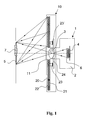
- FIGURE shows a schematic view of an optoelectronic sensor with a pick-up system and incident-light illumination device.
- the optoelectronic sensor shown in Fig. 1 has a recording system 1, which has a receiving objective 3 and a light receiving unit 4 in a housing 2.
- This light receiving unit 4 may consist of a single photosensitive element or, as shown in Fig. 1, a plurality of photosensitive elements constructed in CMOS or CCD technology.
- the reception objective 3 from the recording system 1 an image of an object plane 5 on the surface 6 of the light receiving unit 4 is generated.
- the light receiving unit 4 consists of a matrix-shaped two-dimensional light receiver, as known from a digital camera, the image can be read out from the object plane 5 and fed to an image processing unit, not shown here. If, as also shown in FIG.
- an object 7 is located in the object plane 5, in particular the features of the object surface on the surface 6 of the light receiving unit 4 are reproduced by the object 7.
- the recording system 1 is provided with an inherent incident illumination device 10.
- This incident illumination device 10 has in its outer shape substantially the shape of a flat disc with a central opening 11. Through this central opening 11 through the receiving system 1 can take the image of the object plane 5.
- the main component in the incident illumination device 10 is an optical functional element 20 having a rear optical interface 21 and an object plane indicative interface 22.
- a plurality of light sources 23, 23 ' shown here in the form of LEDs. on a circuit board 24 arranged.
- the light emitted by the light sources 23 is coupled directly into the optical functional element 20.
- the light sources 23 can be fixedly connected to the optical functional element 20 via an optical contact means, or the light sources 23 couple their light into the optical functional element 20 via a small air gap.
- the rear optical interface 21 and / or the surface 22 indicative of the object plane are provided with a location-dependent surface profile (not shown in detail). Depending on the task, this surface profile is composed of several different types of optical elements.
- the optical interface 21 and / or the boundary surface 22 indicative of the object plane is partially provided with a location-dependent mirror layer and / or an imprint.
- a volume-scattering material is used as the material for the optical functional element 20.
- the two boundary surfaces 21 and 22 of the optical functional element 20 have a slightly spherical, aspherical or spline curve.
Abstract
Description
Die Erfindung betrifft einen optoelektronischen Sensor zur berührungslosen Erfassung von Objekten nach dem Oberbegriff des Anspruchs 1.The invention relates to an optoelectronic sensor for non-contact detection of objects according to the preamble of
Derartige Sensoren werden zum Beispiel in einem Fertigungsprozess eingesetzt, um die Anwesenheit eines Objektes innerhalb eines Bereiches detektieren zu können. Dieses Erkennen ist oft mit weiteren Funktionen wie zum Beispiel einer positionsgenauen Lageerkennung, einer Sortier- oder Selektionsfunktion usw. verbunden.
Zu diesem Zweck wird das Objekt mit einer Beleuchtungsvorrichtung angeleuchtet und dabei das am Objekt reflektierte bzw. remittierte Licht mit einem Aufnahmesystem erfasst. Das Aufnahmesystem besteht dabei in der Regel aus einem Empfangsobjektiv und einer in dessen Bildebene angeordneten Lichtempfangseinheit. Je nach der Aufgabe dieses Sensors besteht die Lichtempfangseinheit aus einem oder mehreren lichtempfindlichen Elementen. In diesem Sinn kann ein derartiges Aufnahmesystem aus einer einfachen Lichtschranke mit zum Beispiel einer einzelnen positionsempfindlichen Lichtempfangseinheit oder einer digitalen Kamera bestehen. Im Falle einer Kamera ist die Lichtempfangseinheit meist eine matrixförmige Anordnung von mehreren lichtempfindlichen Elementen, die in CMOS- oder CCD-Technologie aufgebaut sind. Außerdem ist beim Einsatz einer Kameraausführung in der Regel ein geeignetes Auswertungssystem zur Bildverarbeitung nachgeschaltet.Such sensors are used, for example, in a manufacturing process to detect the presence of an object within a range can. This recognition is often associated with other functions such as a positionally accurate position detection, a sorting or selection function, etc.
For this purpose, the object is illuminated with a lighting device, thereby detecting the object reflected or remitted light with a recording system. As a rule, the recording system consists of a receiving objective and a light receiving unit arranged in its image plane. Depending on the task of this sensor, the light receiving unit consists of one or more photosensitive elements. In this sense, such a recording system may consist of a simple light barrier with, for example, a single position-sensitive light-receiving unit or a digital camera. In the case of a camera, the light receiving unit is usually a matrix arrangement of a plurality of photosensitive elements, which are constructed in CMOS or CCD technology. In addition, when using a camera design, a suitable evaluation system for image processing is usually connected downstream.
Um eine möglichst hohe Zuverlässigkeit beim Betrieb einer derartigen Sensoreinrichtung zu gewährleisten, ist es insbesondere bei nicht kooperativen Objekten notwendig, das Aufnahmesystem mit einer optimalen Beleuchtungsvorrichtung zu verbinden.
Die nach dem Stand der Technik bekannten Beleuchtungsvorrichtungen sind beispielsweise mit Glühlampen, LEDs oder mit Laserquellen ausgestatteten Leuchtmittel bestückt, deren Licht teilweise auch mit herkömmlichen Linsen oder Glasfasern auf die Objekte gerichtet wird.In order to ensure the highest possible reliability in the operation of such a sensor device, it is necessary in particular for non-cooperative objects, to connect the recording system with an optimal lighting device.
The lighting devices known from the prior art are, for example, equipped with incandescent lamps, LEDs or lamps equipped with laser sources, the light of which is also partially directed to the objects with conventional lenses or glass fibers.
Der Begriff "Licht" ist dabei nicht auf das sichtbare Licht beschränkt. Unter "Licht" sind allgemein elektromagnetische Strahlen, also UV-Licht, IR-Licht sowie sichtbares Licht zu verstehen, welche üblicherweise für den Betrieb von optoelektronischen Sensoren eingesetzt werden können.The term "light" is not limited to the visible light. Under "light" are generally electromagnetic radiation, ie UV light, IR light and visible light to understand, which can usually be used for the operation of optoelectronic sensors.
Derartige nach dem Stand der Technik bekannte optoelektronische Sensoren haben im Einsatzfall oft Probleme, wenn Objekte, deren Oberfläche einen hohen Glanzanteil aufweisen, sicher erkannt werden sollen. Die Probleme sind darin begründet, dass, wenn ein Objekt mit hohem Glanzanteil auf der Oberfläche mit einem gerichteten Lichtstrahl beleuchtet wird, durch den Glanzanteil am Objekt das reflektierte Licht in eine Richtung reflektiert werden kann, die außerhalb der Öffnung des Empfangsobjektivs liegt. In diesem Fall sind die Bildinhalte, die dem Glanzanteil des Objektes zugeordnet sind, auf der Lichtempfangseinheit dunkel und damit nicht oder nur bedingt auswertbar. Gleiches gilt für den Fall, wenn das am Glanzanteil des Objektes reflektierte Licht der Beleuchtungsvorrichtungen in die Öffnung des Empfangsobjektivs einfällt und dadurch auf der Lichtempfangseinheit eine sehr hohe Leuchtdichte entsteht. Die dadurch entstehenden Hot Spots vermindern die Bildqualität derart, dass die Erkennungsleistung des optoelektronischen Sensors stark herabgesetzt wird.
Zur Umgehung dieser Probleme ist es nach dem Stand der Technik bekannt, das Objekt mit einer Dome-Beleuchtung auszuleuchten. Bei einer Dome-Beleuchtung wird das zu beleuchtende Objekt von einer nahezu halbkugelförmigen Haube umschlossen. Diese halbkugelförmige Haube ist auf ihrer Innenfläche mit einer diffus reflektierenden Oberflächenschicht belegt. Gleichzeitig sind mehrere breitstreuende Lichtquellen angeordnet, die insbesondere die Innenwand der halbkugelförmigen Haube und damit auch das Objekt anleuchten. Auf diese Weise wird das Objekt aus einem großen Raumwinkelbereich heraus angeleuchtet. Diese, für die Ausleuchtung des Objektes an sich gute Dome-Beleuchtung, bringt jedoch im praktischen Einsatz mehrere Nachteil mit sich. So ist insbesondere die große Bauhöhe von Nachteil, die den Freiraum zwischen dem Sensor und der Objektebene stark einschränkt. Ein weiterer Nachteil dieser Dome-Beleuchtung ist darin zu sehen, weil eine derart große Beleuchtungsvorrichtung nicht mehr sinnvoll mit dem Aufnahmesystem zu einer Einheit integriert werden kann.Such known in the art optoelectronic sensors often have problems in the application, when objects whose surface has a high gloss ratio to be reliably detected. The problems are due to the fact that when a high gloss object on the surface is illuminated with a directional light beam, the reflected light can be reflected by the gloss level of the object in a direction that is outside the aperture of the receiving lens. In this case, the image contents, which are assigned to the gloss component of the object, are dark on the light receiving unit and thus can not be evaluated or only conditionally evaluated. The same applies to the case when the light reflected by the gloss component of the object of the illumination devices incident in the opening of the receiving lens and thereby produces a very high luminance on the light receiving unit. The resulting hot spots reduce the image quality such that the detection performance of the optoelectronic sensor is greatly reduced.
To circumvent these problems, it is known in the art to illuminate the object with a dome illumination. In a dome lighting, the object to be illuminated is enclosed by a nearly hemispherical hood. This hemispherical hood is covered on its inner surface with a diffusely reflecting surface layer. At the same time, a plurality of wide-scattering light sources are arranged, which in particular illuminate the inner wall of the hemispherical hood and thus also the object. In this way, the object is illuminated from a large solid angle range out. This, for the illumination of the object itself good dome illumination, however, brings in practical use several disadvantages. So in particular the large height of Disadvantage that severely limits the space between the sensor and the object plane. Another disadvantage of this dome lighting is to be seen in that such a large lighting device can no longer be meaningfully integrated with the recording system to form a unit.
Der Erfindung liegt deshalb die Aufgabe zugrunde, mit einer möglichst flachen Beleuchtungsvorrichtung, die inhärent mit dem Aufnahmesystem verbunden ist, ein in der Objektebene befindliches Objekt möglichtst diffus aus einem großen Raumwinkelbereich heraus zu beleuchten.The invention is therefore based on the object, with a flat as possible lighting device that is inherently connected to the recording system, a object located in the object level allows diffuse lighting from a large solid angle range out.
Die Lösung dieser Aufgabe erfolgt durch die Merkmale des Anspruchs 1. Danach wird ein optoelektronischer Sensor zur berührungslosen Erfassung von Objekten bzw. Objektmerkmalen beschrieben, der ein Aufnahmesystem mit einem Empfangsobjektiv und einer Lichtempfangseinheit aufweist. Gleichzeitig ist bei diesem Sensor mit dem Aufnahmesystem inhärent eine Auflichtbeleuchtungsvorrichtung verbunden, mit der die Objektebene ausgeleuchtet wird. Erfindungsgemäß ist dabei vorgesehen, dass die inhärente Auflichtbeleuchtungsvorrichtung in ihrer Außenform im Wesentlichen die Form einer flachen Scheibe aufweist, welche das Empfangsobjektiv rotationssymmetrisch umschließt. Dabei besitzt die Auflichtbeleuchtungsvorrichtung eine zentrale Öffnung, durch die das am Objekt remittierte Licht ins Empfangsobjektiv eintreten kann. Durch diese erfindungsgemäße konstruktive Ausgestaltung bilden das Aufnahmesystem und die Auflichtbeleuchtungsvorrichtung eine kompakte Einheit, bei der auch die erforderlichen elektrischen Versorgungs- und Datenleitungen der beiden Komponenten in vorteilhafter Weise zusammengefasst sind. Nach der Erfindung befindet sich innerhalb der scheibenförmigen Auflichtbeleuchtungsvorrichtung ein an die Größe der Außenform angepasstes optisches Funktionselement, in dessen Grenzfläche, die dem Objekt abgewandt ist, mehrere Lichtquellen ihr ausgesandtes Licht einkoppeln und aus der dem Objekt zugewandten Grenzfläche das Licht gleichmäßig verteilt austritt und so die Objektebene mit homogener Leuchtstärkeverteilung ausleuchtet.
Besonders vorteilhaft ist es dabei, wenn der Außendurchmesser des optischen Funktionselementes vielfach größer als der wirksame Öffnungsdurchmesser des Empfangsobjektives ist, weil dadurch auch die Flächenanteile eines Objektes, die stark geneigt zur optischen Achse des Empfangsobjektives angeordnet sind, das gesamte Gesichtfeld noch gut ausleuchten.The solution of this object is achieved by the features of
It is particularly advantageous if the outer diameter of the optical functional element is often greater than the effective aperture diameter of the receiving lens, because thereby also the surface portions of an object, which are arranged greatly inclined to the optical axis of the receiving lens, the entire field of vision still well.
Weiterhin ist es vorteilhaft, dass das aus dem optischen Funktionselement austretende Licht die Objektebene diffus ausleuchtet, weil dadurch mögliche Glanzstellen auf dem Objekt keine Erkennungsfehler durch Dunkelzonen bzw. durch Hot Spots in der Bildebene hervorrufen.
In einer bevorzugten Ausführungsform der Erfindung sind die Lichtquellen ohne Luftspalt, d. h. über ein geeignetes optisches Kontaktmittel mit dem optischen Funktionselement verbunden. Auf diese Weise sind keine optischen Grenzflächen zwischen zum Beispiel einer LED und dem optische Funktionselement vorhanden, so dass dadurch der Einkoppelwirkungsgrad des Lichtes von der LED in das optische Funktionselement erhöht ist.
In einer anderen Ausführung sind die Lichtquellen über eine lösbare Verbindung mit dem optischen Funktionselement verbunden. Diese Ausführungsform ist insbesondere dann vorteilhaft, wenn zum Beispiel die optischen Funktionselemente zum Zwecke der Anpassung an verschiedene Objektabstände oder zur Veränderung der Größe der ausgeleuchteten Fläche in der Objektebene ausgewechselt werden sollen.Furthermore, it is advantageous that the light emerging from the optical functional element illuminates the object plane in a diffuse manner, because thereby possible highlights on the object do not cause any recognition errors due to dark zones or hot spots in the image plane.
In a preferred embodiment of the invention, the light sources without an air gap, that is connected via a suitable optical contact means with the optical functional element. In this way, there are no optical interfaces between, for example, an LED and the optical functional element, so that thereby the coupling efficiency of the light from the LED into the optical functional element is increased.
In another embodiment, the light sources are connected via a detachable connection with the optical functional element. This embodiment is particularly advantageous if, for example, the optical functional elements for the purpose of adaptation to different object distances or to change the size of the illuminated area in the object plane to be replaced.
Eine vorteilhafte Ausgestaltung der rückseitigen optischen Grenzfläche des optischen Funktionselementes sieht vor, dass diese zumindest teilweise ein ortsabhängiges Oberflächenprofil aufweist. Dieses ortsabhängige Oberflächenprofil kann dabei aus Linsen, Keilflächen oder Verlaufflächen gebildet sein. Dabei ist es auch vorgesehen, diese Elemente in Mikroform, Fresnelform oder als diffraktive Elemente auszuführen. Mit einem derartigen Oberflächenprofil auf der rückseitigen optischen Grenzfläche ist es möglich, durch Ausstreuungen und/oder durch Ablenkungen den Verlauf des eingekoppelten Lichtes gezielt zu beeinflussen.
Vorteilhaft ist es weiterhin, wenn das optische Funktionselement auf der rückseitigen optischen Grenzfläche zumindest teilweise mit einer Spiegelschicht versehen ist. Auf diese Weise kann auch das im Funktionselement eingekoppelte Licht, welches unter einem kleineren Winkel als dem Grenzwinkel der Totalreflexion von der Innenseite kommend auf die Grenzfläche trifft, in dem Funktionselement gehalten werden. Dies erhöht den Wirkungsgrad der Auflichtbeleuchtungsvorrichtung.
Eine weitere Ausführungsform der Erfindung sieht vor, dass auf der rückseitigen Grenzfläche das optische Funktionselement zumindest teilweise mit einer nichtmetallischen Beschichtung bzw. Bedruckung versehen ist. Mit diesen partiell unterschiedlich starken bzw. dichten Beschichtungen/Bedruckungen ist es möglich, dass die Homogenität der Lichtverteilung beim Lichtaustritt aus dem Funktionselement in vorteilhafter Weise in weiten Grenzen beeinflusst wird.
Analog zu den Gestaltungsformen für die rückseitige Grenzfläche des optischen Funktionselementes ist es in weiteren vorteilhaften Ausführungen der Erfindung vorgesehen, alternativ oder gleichzeitig auch die zur Objektebene hinweisende Fläche des optischen Funktionselement mit einer Profilierung und/oder Beschichtung bzw. Bedruckung zu versehen.
Außerdem ist es von Vorteil, wenn das optische Funktionselement einen deutlich größeren Flächenanteil als die ausgeleuchtete Objektebene aufweist. Durch diese Maßnahme wird ein Objekt, das sich in der Objektebene befindet, aus einem gro-ßen Raumwinkelbereich heraus beleuchtet. Damit ist es möglich, dass auch Flächenanteile von einem Objekt, das geneigt zur optischen Achse des Empfangsobjektives angeordnet ist, das gesamte Gesichtfeld noch gut ausleuchten.
Eine Homogenisierung der Lichtverteilung kann nach der Erfindung in vorteilhafter Weise auch dadurch erreicht werden, dass das optische Funktionselement aus einem Werkstoff hergestellt ist, der zumindest teilweise eine Volumenstreuung aufweist.
In einer vorteilhaften Erweitung sind dem Werkstoff für das optische Funktionselement, der zum Beispiel aus Polycarbonat besteht, noch Glasfaseranteile beigemischt.
Es ist weiterhin als vorteilhaft anzusehen, wenn das optische Funktionselement rotationssymmetrisch eine unterschiedliche Dicke hat. So kann zum Beispiel das an sich flache optische Funktionselement in seinem Mittenbereich eine größere Materialstärke aufweisen und somit die Form eines Kegels mit einem sehr stumpfem Kegelwinkel haben. Weiterhin ist auch vorgesehen, dass eine oder beide der Grenzflächen des optischen Funktionselementes eine leicht sphärische, ashärische oder spline Kurve aufweisen. Mit diesen geometrischen Varianten bei der Form des Funktionselementes ist möglich, neben der Homogenisierung der Lichtverteilung auch die Abstrahlrichtung des Lichtes zwischen dem Funktionselement und der ausgeleuchteten Objektebene zu beeinflussen.
Unter dem Gesichtspunkt einer kostengünstigen und kleinvolumigen Bauform ist es vorteilhaft, wenn die Lichtquellen ringförmig im Mittenbereich unmittelbar um das Empfangsobjektiv herum angeordnet sind. In diesem Fall sind zum Beispiel die LED's alle auf einer scheibenförmigen Leiterplatte angeordnet, wodurch der elektrische Verdrahtungsaufwand innerhalb der inhärenten Auflichtbeleuchtungsvorrichtung deutlich minimiert ist.An advantageous embodiment of the rear optical interface of the optical functional element provides that this at least partially has a location-dependent surface profile. This location-dependent surface profile can be formed from lenses, wedge surfaces or course surfaces. It is also intended to carry out these elements in microform, Fresnel or as diffractive elements. With such a surface profile on the rear optical interface, it is possible to selectively influence the course of the injected light by scattering and / or by distractions.
It is furthermore advantageous if the optical functional element on the rear optical interface is at least partially provided with a mirror layer. In this way, the light coupled in the functional element, which impinges on the boundary surface at a smaller angle than the limiting angle of the total reflection coming from the inside, can be held in the functional element. This increases the efficiency of incident light illumination device.
A further embodiment of the invention provides that the optical functional element is at least partially provided with a non-metallic coating or printing on the rear boundary surface. With these partially different thick or dense coatings / prints, it is possible that the homogeneity of the light distribution at the light exit from the functional element is advantageously influenced within wide limits.
Analogous to the design forms for the rear interface of the optical functional element, it is provided in further advantageous embodiments of the invention, alternatively or simultaneously, to provide the surface of the optical functional element indicative of the object plane with a profiling and / or coating or printing.
Moreover, it is advantageous if the optical functional element has a significantly larger area fraction than the illuminated object plane. As a result of this measure, an object that is located in the object plane is illuminated from a large solid angle range. This makes it possible that surface portions of an object which is arranged inclined to the optical axis of the receiving lens, the entire field of view still well.
A homogenization of the light distribution can also be achieved according to the invention in an advantageous manner in that the optical functional element is made of a material which has at least partially a volume scattering.
In an advantageous extension of the material for the optical functional element, which consists for example of polycarbonate, glass fiber shares still admixed.
It can also be regarded as advantageous if the optical functional element has rotationally symmetrical different thickness. Thus, for example, the inherently flat optical functional element can have a greater material thickness in its central region and thus have the shape of a cone with a very blunt cone angle. Furthermore, it is also provided that one or both of the boundary surfaces of the optical functional element have a slightly spherical, ashärische or spline curve. With these geometric variants in the shape of the functional element is possible to influence not only the homogenization of the light distribution but also the emission direction of the light between the functional element and the illuminated object plane.
From the point of view of a cost-effective and small-volume design, it is advantageous if the light sources are arranged annularly in the middle region directly around the receiving lens. In this case, for example, the LEDs are all arranged on a disc-shaped circuit board, whereby the electrical Wiring costs within the inherent incident illumination device is significantly minimized.
Die Erfindung wird im Folgenden beispielhaft unter Bezugnahme auf die Zeichnung beschrieben, deren einzige Figur 1 eine schematische Ansicht eines optoelektronischen Sensors mit einem Aufnahmesystem und einer Auflichtbeleuchtungsvorrichtung zeigt.The invention is described below by way of example with reference to the drawing, the single FIGURE of which shows a schematic view of an optoelectronic sensor with a pick-up system and incident-light illumination device.
Der in Fig. 1 gezeigte optoelektronische Sensor hat ein Aufnahmesystem 1, welches in einem Gehäuse 2 ein Empfangsobjektiv 3 und eine Lichtempfangseinheit 4 aufweist. Diese Lichtempfangseinheit 4 kann aus einem einzelnen lichtempfindlichen Element oder, wie es in Fig. 1 dargestellt ist, aus einer Vielzahl von lichtempfindlichen Elementen, die in CMOS- oder CCD-Technologie aufgebaut sind, bestehen. Mit dem Empfangsobjektiv 3 aus dem Aufnahmesystem 1 wird ein Abbild von einer Objektebene 5 auf der Oberfläche 6 der Lichtempfangseinheit 4 erzeugt. Wenn die Lichtempfangseinheit 4 zum Beispiel aus einem in Matrixform aufgebauten zweidimensionalen Lichtempfänger besteht, kann, wie dies von einer Digitalkamera bekannt ist, das Abbild von der Objektebene 5 ausgelesen und einer hier nicht dargestellten Bildverarbeitungseinheit zugeführt werden.
Befindet sich, wie ebenfalls in Fig. 1 dargestellt, ein Objekt 7 in der Objektebene 5, so werden von dem Objekt 7 insbesondere die Merkmale der Objektoberfläche auf der Oberfläche 6 der Lichtempfangseinheit 4 wiedergegeben. Für die Qualität dieser Abbildung ist neben der Güte des Empfangsobjektivs 3 von zentraler Bedeutung, wie das Objekt 7 in der Objektebene 5 beleuchtet ist. Um einen großen Informationsinhalt aus dem Abbild des Objekts 7 erfassen zu können, ist es notwendig, das Objekt 7 mit gleichmäßiger Beleuchtungsstärke, die aus einem möglicht großen Raumwinkelbereich heraus erzeugt wird, diffus auszuleuchten. Zu diesem Zweck ist das Aufnahmesystem 1 mit einer inhärenten Auflichtbeleuchtungsvorrichtung 10 versehen. Diese Auflichtbeleuchtungsvorrichtung 10 hat in seiner Außenform im Wesentlichen die Form einer flachen Scheibe mit einer zentralen Öffnung 11. Durch diese zentrale Öffnung 11 hindurch kann das Aufnahmesystem 1 das Abbild von der Objektebene 5 aufnehmen. Die Hauptkomponente in der Auflichtbeleuchtungsvorrichtung 10 ist ein optisches Funktionselement 20 mit einer rückseitigen optischen Grenzfläche 21 und einer zur Objektebene hinweisenden Grenzfläche 22. Unmittelbar angrenzend an die rückseitige optische Grenzfläche 21 sind mehrere Lichtquellen 23, 23', die hier in Form von LED's dargestellt sind, auf einer Leiterplatte 24 angeordnet. Das von den Lichtquellen 23 ausgesandte Licht wird unmittelbar in das optische Funktionselement 20 eingekoppelt. Zu diesem Zweck können die Lichtquellen 23 über ein optisches Kontaktmittel fest mit dem optischen Funktionselement 20 verbunden sein oder die Lichtquellen 23 koppeln ihr Licht über einen geringen Luftspalt in das optische Funktionselement 20 ein. Die rückseitige optische Grenzfläche 21 und/oder die zur Objektebene hinweisende Grenzfläche 22 sind mit einem im Detail nicht dargestellten ortsabhängigen Oberflächenprofil versehen. Dieses Oberflächenprofil setzt sich je nach Aufgabenstellung aus mehreren verschiedenenartigen optischen Elementen zusammen. Dabei haben diese Elemente die Form von einzelnen Linsen, Keilflächen oder Verlaufflächen. In einer speziellen Ausführungsform ist die optische Grenzfläche 21 und/oder die zur Objektebene hinweisende Grenzfläche 22 partiell noch mit einer ortsabhängigen Spiegelschicht und/oder einer Bedruckung versehen.
In einer weiteren Ausführungsform ist es vorgesehen, dass als Werkstoff für das optische Funktionselement 20 ein volumenstreuendes Material verwendet wird. Ebenso ist es auch vorgesehen, dass die beiden Grenzflächen 21 und 22 des optischen Funktionselementes 20 eine leicht sphärische, asphärische oder spline Kurve aufweisen.
Mit diesen optischen Maßnahmen innerhalb und an den beiden Grenzflächen 21 und 22 des optischen Funktionselements 20 wird erreicht, dass das von den Lichtquellen 23 in die rückseitige optische Grenzfläche 21 eingekoppelte Licht weitgehend homogen aus der zur Objektebene hinweisenden Grenzfläche 22 austritt und damit die Objektebene 5 diffus ausleuchtet.The optoelectronic sensor shown in Fig. 1 has a
If, as also shown in FIG. 1, an
In a further embodiment, it is provided that a volume-scattering material is used as the material for the optical
It is achieved with these optical measures within and at the two
Claims (23)
Applications Claiming Priority (1)
| Application Number | Priority Date | Filing Date | Title |
|---|---|---|---|
| DE102006023142A DE102006023142A1 (en) | 2006-05-16 | 2006-05-16 | Camera lighting unit |
Publications (2)
| Publication Number | Publication Date |
|---|---|
| EP1857873A2 true EP1857873A2 (en) | 2007-11-21 |
| EP1857873A3 EP1857873A3 (en) | 2013-07-10 |
Family
ID=38331690
Family Applications (1)
| Application Number | Title | Priority Date | Filing Date |
|---|---|---|---|
| EP07008730.9A Withdrawn EP1857873A3 (en) | 2006-05-16 | 2007-04-28 | Camera illumination unit |
Country Status (2)
| Country | Link |
|---|---|
| EP (1) | EP1857873A3 (en) |
| DE (1) | DE102006023142A1 (en) |
Cited By (1)
| Publication number | Priority date | Publication date | Assignee | Title |
|---|---|---|---|---|
| EP3026470A1 (en) * | 2009-10-30 | 2016-06-01 | Fujitsu Frontech Limited | Prism plate, illumination optical system of imaging device, and forming die of prism plate |
Families Citing this family (3)
| Publication number | Priority date | Publication date | Assignee | Title |
|---|---|---|---|---|
| DE102011008328B4 (en) * | 2011-01-11 | 2022-03-17 | Baumer Electric Ag | Optical sensor with colored front screen |
| DE102013105105B3 (en) | 2013-05-17 | 2014-11-06 | Sick Ag | 3D camera with at least one lighting device |
| DE202013102178U1 (en) | 2013-05-17 | 2014-08-18 | Sick Ag | Illumination device for generating a lighting area for a 3D camera |
Citations (11)
| Publication number | Priority date | Publication date | Assignee | Title |
|---|---|---|---|---|
| US3474242A (en) * | 1966-10-14 | 1969-10-21 | David W Forrant | Photographic ring light |
| US5690417A (en) * | 1996-05-13 | 1997-11-25 | Optical Gaging Products, Inc. | Surface illuminator with means for adjusting orientation and inclination of incident illumination |
| US6022124A (en) * | 1997-08-19 | 2000-02-08 | Ppt Vision, Inc. | Machine-vision ring-reflector illumination system and method |
| US6033087A (en) * | 1996-12-26 | 2000-03-07 | Patlite Corporation | LED illuminating device for providing a uniform light spot |
| US6053621A (en) * | 1996-07-08 | 2000-04-25 | Ccs Co., Ltd. | Lighting unit for inspecting a surface |
| EP1158460A2 (en) * | 2000-05-26 | 2001-11-28 | Sick AG | Image processing system and method |
| US6429934B1 (en) * | 1998-09-11 | 2002-08-06 | Robotic Vision Systems, Inc. | Optimal symbology illumination-apparatus and method |
| WO2002073953A2 (en) * | 2001-03-08 | 2002-09-19 | Hand Held Products, Inc. | Optical reader imaging module |
| US20020191299A1 (en) * | 2001-06-19 | 2002-12-19 | Jain Ajaykumar R. | Optical device for dispersion compensation |
| US20030161024A1 (en) * | 2002-02-27 | 2003-08-28 | Qin Zhang | Dual fibers coupled to an etalon |
| WO2005031392A2 (en) * | 2003-09-26 | 2005-04-07 | Ramot At Tel-Aviv University Ltd. | Integrated microlens reflector and light coupler |
-
2006
- 2006-05-16 DE DE102006023142A patent/DE102006023142A1/en not_active Withdrawn
-
2007
- 2007-04-28 EP EP07008730.9A patent/EP1857873A3/en not_active Withdrawn
Patent Citations (11)
| Publication number | Priority date | Publication date | Assignee | Title |
|---|---|---|---|---|
| US3474242A (en) * | 1966-10-14 | 1969-10-21 | David W Forrant | Photographic ring light |
| US5690417A (en) * | 1996-05-13 | 1997-11-25 | Optical Gaging Products, Inc. | Surface illuminator with means for adjusting orientation and inclination of incident illumination |
| US6053621A (en) * | 1996-07-08 | 2000-04-25 | Ccs Co., Ltd. | Lighting unit for inspecting a surface |
| US6033087A (en) * | 1996-12-26 | 2000-03-07 | Patlite Corporation | LED illuminating device for providing a uniform light spot |
| US6022124A (en) * | 1997-08-19 | 2000-02-08 | Ppt Vision, Inc. | Machine-vision ring-reflector illumination system and method |
| US6429934B1 (en) * | 1998-09-11 | 2002-08-06 | Robotic Vision Systems, Inc. | Optimal symbology illumination-apparatus and method |
| EP1158460A2 (en) * | 2000-05-26 | 2001-11-28 | Sick AG | Image processing system and method |
| WO2002073953A2 (en) * | 2001-03-08 | 2002-09-19 | Hand Held Products, Inc. | Optical reader imaging module |
| US20020191299A1 (en) * | 2001-06-19 | 2002-12-19 | Jain Ajaykumar R. | Optical device for dispersion compensation |
| US20030161024A1 (en) * | 2002-02-27 | 2003-08-28 | Qin Zhang | Dual fibers coupled to an etalon |
| WO2005031392A2 (en) * | 2003-09-26 | 2005-04-07 | Ramot At Tel-Aviv University Ltd. | Integrated microlens reflector and light coupler |
Cited By (1)
| Publication number | Priority date | Publication date | Assignee | Title |
|---|---|---|---|---|
| EP3026470A1 (en) * | 2009-10-30 | 2016-06-01 | Fujitsu Frontech Limited | Prism plate, illumination optical system of imaging device, and forming die of prism plate |
Also Published As
| Publication number | Publication date |
|---|---|
| EP1857873A3 (en) | 2013-07-10 |
| DE102006023142A1 (en) | 2007-11-22 |
Similar Documents
| Publication | Publication Date | Title |
|---|---|---|
| DE69931503T2 (en) | DEVICE AND METHOD FOR DIFFUSING LIGHTING OF A SURFACE | |
| DE19526512B4 (en) | Lighting device for vehicles | |
| EP1727678B1 (en) | Optical system for creating an illuminated structure | |
| EP1730500B1 (en) | Optical system for creating an illuminating strip | |
| DE60033475T2 (en) | Integrated light mixer | |
| DE102013225950B4 (en) | Automotive lighting device | |
| AT500056A1 (en) | OPTIC ELEMENT FOR TRAFFIC SIGNS, INDICATOR TABLES OR DGL. | |
| DE10219246A1 (en) | Lighting device for motor vehicles | |
| DE102010041096A1 (en) | lighting device | |
| DE112008001114B4 (en) | Device for surface inspection | |
| DE112015002290T5 (en) | PICTURE MODULE, READER AND METHOD FOR LIGHTING AND PICTURE OF OBJECTIVES WHICH SHOULD BE READ OVER AN EXTENDED FIELD OF WORK DISTANCE | |
| DE102008044003A1 (en) | Camera module with multiple function | |
| EP2784376A2 (en) | Motor vehicle light for dynamic light functions | |
| DE102019131098A1 (en) | LIDAR INTEGRATED LIGHTING DEVICE FOR A VEHICLE | |
| EP1857873A2 (en) | Camera illumination unit | |
| DE19511197C2 (en) | Method and device for the optical inspection of a surface, in particular a compact disc | |
| DE102018220106A1 (en) | lamp unit | |
| DE202005011807U1 (en) | Dark field illumination device, for coordinates measuring device, has optical sensor, and light emitting diodes including light emitting openings aligned on common focus point | |
| DE102009058807A1 (en) | Sensor for checking value documents | |
| DE10159234B4 (en) | Device for examining documents | |
| DE102004011987A1 (en) | Optical conduit for directing light onto a surface | |
| DE10323409A1 (en) | Device for checking banknotes | |
| WO2015135676A1 (en) | Image recording device, in particular for vehicle measurement | |
| AT518379A1 (en) | Device for displaying a target | |
| DE102013114325B4 (en) | Optoelectronic sensor and method for detecting shiny objects |
Legal Events
| Date | Code | Title | Description |
|---|---|---|---|
| PUAI | Public reference made under article 153(3) epc to a published international application that has entered the european phase |
Free format text: ORIGINAL CODE: 0009012 |
|
| AK | Designated contracting states |
Kind code of ref document: A2 Designated state(s): AT BE BG CH CY CZ DE DK EE ES FI FR GB GR HU IE IS IT LI LT LU LV MC MT NL PL PT RO SE SI SK TR |
|
| AX | Request for extension of the european patent |
Extension state: AL BA HR MK YU |
|
| PUAL | Search report despatched |
Free format text: ORIGINAL CODE: 0009013 |
|
| AK | Designated contracting states |
Kind code of ref document: A3 Designated state(s): AT BE BG CH CY CZ DE DK EE ES FI FR GB GR HU IE IS IT LI LT LU LV MC MT NL PL PT RO SE SI SK TR |
|
| AX | Request for extension of the european patent |
Extension state: AL BA HR MK RS |
|
| RIC1 | Information provided on ipc code assigned before grant |
Ipc: G03B 15/03 20060101AFI20130605BHEP Ipc: H04N 5/225 20060101ALI20130605BHEP |
|
| STAA | Information on the status of an ep patent application or granted ep patent |
Free format text: STATUS: THE APPLICATION HAS BEEN WITHDRAWN |
|
| 18W | Application withdrawn |
Effective date: 20130723 |