EP1865400A1 - Method for switching an internal clock and clock synchronisation device - Google Patents
Method for switching an internal clock and clock synchronisation device Download PDFInfo
- Publication number
- EP1865400A1 EP1865400A1 EP07010923A EP07010923A EP1865400A1 EP 1865400 A1 EP1865400 A1 EP 1865400A1 EP 07010923 A EP07010923 A EP 07010923A EP 07010923 A EP07010923 A EP 07010923A EP 1865400 A1 EP1865400 A1 EP 1865400A1
- Authority
- EP
- European Patent Office
- Prior art keywords
- signal
- clock
- clk
- control module
- hold
- Prior art date
- Legal status (The legal status is an assumption and is not a legal conclusion. Google has not performed a legal analysis and makes no representation as to the accuracy of the status listed.)
- Withdrawn
Links
Images


Classifications
-
- G—PHYSICS
- G06—COMPUTING; CALCULATING OR COUNTING
- G06F—ELECTRIC DIGITAL DATA PROCESSING
- G06F1/00—Details not covered by groups G06F3/00 - G06F13/00 and G06F21/00
- G06F1/04—Generating or distributing clock signals or signals derived directly therefrom
- G06F1/08—Clock generators with changeable or programmable clock frequency
Definitions
- the present invention relates to a method according to the preamble of patent claim 1 for switching a system clock from a first clock signal to a second clock signal, wherein the switching operation is triggered by a selection control signal and the switching takes place synchronously to the first and / or second clock signal.
- the present invention relates to a clock synchronization device for an electronic system, in particular for a microprocessor, according to the preamble of patent claim 6, comprising a first input for a first clock signal, a second input for a second clock signal, a third input for a selection control signal and an output for a system clock signal.
- the present invention relates to a processor unit and a use of the method according to the invention.
- a processor unit in the form of a microprocessor For control of electronic systems, such as in particular a processor unit in the form of a microprocessor, it is regularly necessary to make an application-specific selection of a plurality of externally applied asynchronous clock signals. Depending on the requirement profile a regular switching between different clock signals to output a correspondingly changed system clock signal may be required. However, such a switching operation is also required in particular if one of the external clock signals is faulty or if a corresponding external clock signal source completely fails.
- a disadvantage of the circuit arrangement described above and executable in their use method is that due to the analog circuit elements used no sufficient synthesis capability by means of common (software) synthesis tools is given, also requires the at least partially analogous design of the existing asynchronous state machine high effort in the Production, which is reflected in corresponding cost disadvantages. In addition, due to the described asynchronous operation when switching clock extensions and shortenings result, which is negative on the behavior of controlled by the system clock signal electronic systems, such as a microprocessor affects.
- the invention has for its object, while avoiding the disadvantages listed above, a method and an apparatus of the type mentioned in each case evolve to the effect that they do without complex arrangements of circuit elements, in particular analog circuit elements, so that in particular a cheaper production and improved synthesis capability
- no unwanted clock shortening or prolongation should occur.
- the most unrestricted, flexible usability should be ensured.
- a method for switching a system clock from a first clock signal to a second clock signal wherein the switching operation is triggered by a selection control signal and the switching occurs in synchronism with the first and / or second clock signal, characterized in that the clock control is transmitted from a predetermined edge of the first clock signal to a corresponding edge of the second clock signal, wherein a system clock signal after Assuming the first clock signal at a first predetermined logical signal level is held as a system clock hold signal, being waited for a corresponding edge of the second clock signal and wherein in accordance with the second clock signal, the system clock hold signal is reset to a second logic state and at the same time the system clock signal is reactivated using the second clock signal.
- the system clock switching operation is triggered by the selection control signal, it is then fully executed in accordance with the first and second clock signals which synchronously transfer the clock timing to each other according to the interplay described above.
- an electronic system clock synchronization device in particular for a microprocessor, has: a first input for a first clock signal, a second input for a second clock signal, a third input for a selection control signal and an output for a system clock signal, characterized by a first control module controlled by the first clock signal and a second control module controlled by the second clock signal and signal connected to the first control module, the first control module applying a predetermined signal level of the selection control signal to the first control module third input is formed in synchronism with the first clock signal for setting the system clock signal from the first clock signal to a predetermined logical signal level as a system clock hold signal and wherein the second control module synchronously with the second clock signal for resetting the system clock stop esignals and to Causing an output of the second clock signal is formed as a system clock signal.
- a basic idea of the present invention is thus that the switching over of a system clock signal from a first clock signal to a second clock signal takes place in synchronism with at least one of the first and second clock signals, whereby the undesired clock shortenings and extensions mentioned in the introduction can be avoided.
- the clock synchronization device according to the invention is designed for carrying out such a synchronous switching method such that a completely digital realization is possible, which leads to the desired cost reduction and improved synthesis capability.
- the first and second control modules in the context of a master-slave dependency, a so-called handshake procedure in order to inform each other in a synchronous manner about the triggered switching process and to switch over the system clock.
- a circuit element for generating the system clock hold signal, which is designed to generate a global clock hold signal as a precursor of the system clock hold signal from at least the first and second clock hold signals.
- the relevant circuit element can be designed in particular as a logical OR gate.
- the OR gate transfers a clock hold signal from a first time range (for example, the range of the first clock signal) to a second time range (range of the second clock signal).
- a time has elapsed since the selection control signal was applied is determined and that the switching of the system clock signal is released upon reaching a predetermined time threshold.
- the time threshold can be specified in particular by a user in the course of a software-technical configuration of a system to be controlled.
- a corresponding development of the clock synchronization device provides that at least the first control module has a counter which is designed to determine a time in dependence on the selection control signal.
- the invention provides for a new clock source or a new clock to be switched to recognize and confirm before the actual clock switching takes place. This is done according to the invention by switching on or releasing a safety function (timeout function).
- the safety / timeout function is a simple mechanism that looks for a predetermined skip edge, particularly a rising edge, of the new (system) clock signal before the actual switchover occurs, and that allows switching only when the named one predetermined edge within a predetermined time interval, which is monitored by a corresponding counter.
- the counter determines a time interval within which the slave control module will generate a feedback timing hold signal to be asserted by the master control module can. If the feedback signal is not received within the designated time, the master control module will cancel its originally set clock hold signal and the clock switching operation will be aborted.
- a corresponding timeout logic may also be employed as a means for detecting and controlling a clock switching delay interval, wherein the clock switching delay is in units of periods of the primary system clock signal, that is, the clock signal currently used as system clock. Clock signal acts, can be determined.
- At least the first control module for generating a clock switching inhibit signal as a function of is formed of the selection control signal, which is applied for preventing a resetting of the system clock hold signal to the second control module.
- the first control module is designed to switch off the clock switching blocking signal when a predetermined time threshold is reached.
- the time threshold is at least 2 * T s , where T s denotes a period of the second clock signal (secondary clock signal).
- T s denotes a period of the second clock signal (secondary clock signal).
- the time threshold can be specified by a user, in particular by software technology, the time threshold in particular being at least 2 ⁇ T s , T s designating a period duration of the second clock signal.
- a switching operation is suspended when a corresponding edge of the second clock signal being waited for does not arrive at all or not within a predetermined time window, which indicates, for example, a failed clock source.
- the switching command is held and the previous (first) clock signal is maintained as a system clock.
- Device technology can be provided for this purpose, in particular a further counter.
- only a single counter is used to activate the second clock signal, as described above, and to specify a time window for a fail-safe clock switching.
- first and second clock signals are each selected from a plurality of clock signals. In this way, an optimal application-specific switching of system clock signals is possible.
- the latter each has a multiplexer in operative connection with the first and second inputs, which are used to select the first and the second clock signal are each formed from a plurality of clock signals.
- the clock synchronization device can advantageously be used in particular in a processor unit, in particular in a microprocessor, for controlling the same. Accordingly, there is a preferred use of the method according to the invention for switching the system clock in a processor unit, in particular a microprocessor.
- the present invention provides a clock switching device capable of switching in a synchronous manner from one (first) clock source to another (second) clock source.
- the apparatus basically has first means for selecting a new (second) clock source whose clock signal is to be used as the system clock signal.
- the apparatus has asynchronous means for sampling a clock input which, using cross-coupled sync blocks (control modules), generates a number of control / status signals, in particular clock hold signals.
- the device has means for asynchronously interrogating the control signals (clock hold signals) to generate from these a higher-level global clock stop signal.
- a clock switching delay can be controlled by means of an internal timer.
- a fault protection can be provided, which detects a significant feature of the second clock signal and then decides whether switching to the new (second) clock signal should occur.
- FIG. 1 shows by way of a schematic block diagram an embodiment of a circuit arrangement 1 which, inter alia, has a clock synchronization device 2 according to the invention and which is provided for use with a processor unit such as a microprocessor 3. Notwithstanding the representation in FIG. 1, the circuit arrangement 1 with the clock synchronization device 2 according to the invention can also be integrated into the processor unit 3.
- the circuit arrangement 1 according to FIG. 1 has a first multiplexer 4 and a second multiplexer 5, which are in signal-technical operation with the clock synchronization device 2.
- the first multiplexer 4 has n inputs for external clock signals CLK_1, CLK_2, ..., CLK_n
- the second multiplexer 5 also has n inputs for external clock signals CLK_1, CLK_2, ..., CLK_n.
- the circuit arrangement 1 according to FIG. 1 has a control unit 6, which is in operative signaling connection both with the first and second multiplexers 4, 5 and with the clock synchronization device 2.
- a further input POR for a reset signal is also provided.
- the clock synchronization device 2 has a first input 2.1, a second input 2.2 and a third input 2.3.
- the clock synchronization device 2 has an output 2.4, as well as further connections for a supply voltage VDD, a reference potential (ground or ground) GND and for (user) input values TVAL1, TVAL2, which will be discussed later.
- a first control signal CLK_SEL [n: 1] and a second control signal SW are present.
- the first control signal CLK_SEL [n: 1] is supplied by the processor unit 3 or, deviating from the embodiment of FIG. 1, from a further external unit (not shown) and can refer to the clock signals CLK_1, CLK_2,..., CLK_n be asynchronous.
- the second (external) control signal SW activates the cause of a clock changeover to the clock signal CLK_1, CLK_2,..., CLK_n determined by the first control signal CLK_SEL [n: 1].
- first clock signal CLK_A which was selected by the first multiplexer 4 in accordance with the control unit 6 from the externally predetermined number of clock signals CLK_1, ..., CLK_n.
- a system clock signal SYS_CLK is output to the processor unit 3 by the clock synchronization device 2, whereby the system clock signal SYS_CLK can also be a system clock hold signal, as will also be described in detail below.
- the switching operation triggered by the control unit 6 by means of the selection control signal SEL may be caused, in particular, by faulty or complete failure of a current system clock or arbitrarily by appropriate input, for example by a user, which is known to the person skilled in the art.
- FIG. 2 shows, on the basis of a more detailed block diagram, an embodiment according to the invention of the clock synchronization device 2 according to FIG. 1.
- the same or identically acting elements are provided with the same reference numerals as in FIG.
- the clock synchronization device 2 has two structurally identically designed control modules, namely a first control module (synchronizer) 2.5 and a second control module (synchronizer) 2.6.
- the clock synchronization device 2 has two further circuit elements in the form of a process multiplexer (synchronization state decoder) 2.7 and a logic operation element (clock gate) 2.8, the latter being designed here as an OR gate.
- the first control module 2.5 is connected to input 2.1 of the clock synchronization device 2, so that the first clock signal CLK_A is applied to it.
- the second control module 2.6 is connected to the input 2.2 of the clock synchronization device 2, so that the second clock signal CLK_B is applied to it.
- the switching signal or selection control signal SEL is present both at the first control module 2.5 and at the second control module 2.6.
- Both control modules 2.5, 2.6 also have an input for the reset signal POR.
- a counter element TVAL1 or TVAL2 that is to say a corresponding time interval, can also be predetermined for each control module (cf. FIG. 1), which will be discussed in more detail later.
- the control module 2.5 is configured to output a clock switching inhibit signal flag1; Accordingly, the control module is configured to output a clock switching inhibit signal flag2. Furthermore, the control modules 2.5, 2.6 are each designed to output a gate signal ClkBGate1 or ClkAGate2. Furthermore, the control modules 2.5, 2.6 are each designed to output a clock hold signal hold1 or hold2 and to output a first or a second selection signal SEL_1 or SEL_2.
- the output signals ClkBGate1 and ClkAGate2 are applied to the clock gate 2.8.
- the process multiplexer 2.7 generates from its input signals, to which furthermore the reset signal POR belongs according to FIG. 2, as output signals a delayed selection signal SEL_del and a hold signal hold.
- the first forms, together with the reset signal POR and the already mentioned gate signals CIkBGate1, ClkAGate2 and the first and second clock signals CLK-A, CLK_B, the input signals for the OR gate (clock gate) 2.8, which outputs from it at its output or the output 2.4 of the clock synchronization device 2 according to the invention the system clock signal SYS_CLK.
- FIG. 3 is a detailed block diagram of a first control module of the clock synchronization device of FIG. 2 and FIG. 3 shows a more detailed illustration of the first control module 2.5. It should be emphasized that the second control module 2.6 is constructed structurally identical, so that in the present case an equally detailed description of the same can be dispensed with.
- the first control module 2.5 and correspondingly the second control module 2.6 includes a control block 2.5a, and a state machine 2.5a ', which in turn a counter 2.5b, a holding signal control unit 2.5c, a blocking signal control unit 2.5d and a Gate control unit 2.5e, has.
- the state machine 2.5a has a selection control unit 2.5f and a counter control unit 2.5h and two comparators 2.5i, 2.5j.
- control block 2.5a of the first control module 2.5 of the second control module (not shown) generated clock switching inhibit signal flag2, which is also generated by the second control module clock hold signal hold2 and the switching signal SEL on. Furthermore, the control block 2.5a has the clock switching inhibit signal flag1 generated internally, that is to say within the illustrated first control module 2.5, the gate signal ClkBGate1 and the selection signal SEL_1.
- the control block 2.5 outputs the control signals ASST, CDET, REQD and CNTST, which will be discussed in detail later.
- the above Control signals of the control block 2.5a mentioned are applied to the state machine 2.5a ', as shown in Fig. 3.
- the counter 2.5b In the state machine 2.5a ', the counter 2.5b generates a counter signal or a counter value cnt1, which via an eight-bit line 2.5k both to the holding signal control unit 2.5c and the blocking signal control unit 2.5d and to the comparator 2.5i , 2.5j is delivered.
- the hold signal control unit 2.5c generates the clock hold signal hold1.
- the inhibit signal control unit 2.5d generates the clock switching inhibit signal flag1.
- the gate control unit 2.5e generates the gate signal ClkBGate1.
- the selection control unit 2.5f generates the selection signal SEL_1.
- the counter control unit 2.5h generates a counter enable signal CNTEN.
- control units 2.5c-2.5f except for the counter control unit 2.5h and the counter 2.5b have both the first clock signal CLK_A and the reset signal POR on.
- the comparators 2.5i, 2.5j are in operative connection with the counter control unit 2.5h.
- the switching control signal SEL and the selection signal SEL_1 are applied to the selection control unit 2.5f.
- 4a-d show logic circuit diagrams for illustrating the generation of control signals in a control block according to FIG. 3.
- the signals flag2 and hold2 for generating the control signal ASST are linked by means of a logical AND gate, that is, the control signal ASST has the value "1" (high logic level) when both the clock switching inhibit signal flag2 and the Clock hold signal hold2 has a high logic level.
- the control signal CDET is generated by the clock hold signal hold1 is connected in an inverted form via a logical AND gate to the output of an exclusive OR gate, wherein at the inputs of the exclusive OR gate, the selection signal SEL or Selection signal SEL_1 abut.
- the control signal CDET has a high logic level when either the selection signal SEL or the selection signal SEL_1 has a high logic level and immediately the clock hold signal hold1 has a low logic level.
- the control signal REQD is generated by linking the selection signal SEL_1 via a logical AND gate to the inverted clock switching inhibit signal flag1. In this way, the control signal REQD has a high logic level when the selection signal SEL_1 has a high logic level and the clock switching inhibit signal flag1 has a low logic level.
- the control signal CNTST is generated by a logical AND operation of the selection signal SEL_1 and the gate signal ClkBGate1. In this way, the control signal CNTST has a high logic level when both the selection signal SEL_1 and the gate signal ClkBGate1 have a high logic level.
- Fig. 5 shows in detail a logical circuit arrangement of the counter control unit 2.5h in Fig. 2.
- the counter enable signal CNTEN is generated by first logically ANDing the clock hold signal hold1 with a signal A.
- the signal A represents an output of the comparator 2.5i, which compares the counter value cnt1 of the counter 2.5b with the predetermined end value TVAL1 (cf. FIGS. 1, 2) and a comparator high logic level if: cnt1 ⁇ TVAL1.
- the results of the above-explained logical AND operations in Fig. 5 are then logically ORed so that the counter enable signal CNTEN has a high logic level when either the AND of the signals hold1 and A or the AND of the signals A and B gives a high logic level.
- Fig. 6 shows in detail a circuit construction for generating a clock hold signal. Shown is in particular a circuit structure of the holding signal control unit 2.5c (Fig. 3).
- the circuit arrangement illustrated in FIG. 6 is essentially formed from a sequence of 2-to-1 multiplexers MUX1-MUX7. These act as a changeover switch, which switch in accordance with a respectively applied control or address signal between their two respective inputs. Depending on the logic level of the address signal, either the signal present at the input of the multiplexer designated as "0" (low logic level of the address signal) or the signal present at the input of the multiplexer designated "1" (high logic level of the address signal) is output.
- the input of the multiplexer MUXi designated "0" is also denoted by E0 and the respective input of the multiplexer MUXi denoted by "1” is denoted by E1.
- the clock hold signal hold1 is present at the first multiplexer MUX1, while E1 is at ground potential GND.
- the address signal for MUX1 is generated by a logical AND operation of signals C, D, where C denotes the counter value cnt1 and D denote the set counter end value TVAL1.
- the output of the multiplexer MUX1 is connected to the input E1 of the multiplexer MUX2.
- At the input E0 of the multiplexer MUX2 turn on the clock hold signal hold1.
- the address signal for the multiplexer MUX2 is formed by the control signal CNTEN (see FIGS. 3, 5).
- the output of the multiplexer MUX2 is connected to the input E1 of the multiplexer MUX3, while at the input E0 of the multiplexer MUX3 again the clock hold signal hold 1 is applied.
- the address signal for the multiplexer MUX3 is formed by the control signal CNTST (see FIGS. 3, 4d).
- the output of the multiplexer MUX3 is connected to the input E0 of the multiplexer MUX4, to whose input E1 the power supply signal VDD is applied.
- the address signal for the multiplexer MUX4 is formed by the control signal REQD (cf. FIGS. 3, 4c).
- the output of the multiplexer MUX4 is connected to the input E0 of the multiplexer MUX6.
- the input E1 of the multiplexer MUX6 is connected to the output of the multiplexer MUX5, at whose input E0 the clock hold signal hold1 and at its input E1 again the power supply signal VDD is applied.
- the address signal for the multiplexer MUX5 is formed by a logical AND operation of the inverted clock hold signal hold2 (see FIG. 2) and the inverted gate signal ClkBGate1 (see FIGS. 2, 3).
- the address signal for the multiplexer MUX6 is formed by the control signal CDET (see FIGS. 3, 4b).
- the output of the multiplexer MUX6 is connected to the input E0 of the multiplexer MUX7, at whose input E1 the voltage supply signal VDD is applied.
- the address signal for the multiplexer MUX7 is formed by the control signal ASST (see FIG. 3, 4a).
- the output of the multiplexer MUX7 is connected to the data input D of a flip-flop FF1 connected.
- the flip-flop FF1 is realized as a clock-controlled or clocked flip-flop. At the clock input C is the first clock signal CLK_A on.
- the reset input R of the flip-flop FF1 is connected to the reset signal POR. At the output Q, the flip-flop FF1 outputs the clock hold signal hold1.
- Fig. 7 shows in detail a circuit arrangement for generating a clock switching inhibit signal.
- the circuit arrangement shown in Fig. 7 takes over the function of the blocking signal control unit 2.5d in Fig. 3. It consists of a query of 2-to-1 multiplexers MUX8-MUX10, which act as a changeover switch and inputs E0, E1, a Address or control input and have an output.
- At the input E0 of the multiplexer MUX8 is the clock switching inhibit signal flag1, while input E1 is at ground potential GND.
- the address signal for the multiplexer MUX8 is formed by a logical AND operation of the signals cnt1 and TVAL1 (see FIG. 6).
- the output of the multiplexer MUX8 is connected to the input E1 of the multiplexer MUX9, to whose input E0, in turn, the clock switching inhibit signal flag1 is applied.
- the address signal for the multiplexer MUX9 is formed by the control signal CNTST (see Figs. 3, 4d).
- the output of the multiplexer MUX9 is connected to the input E0 of the multiplexer MUX10, to whose input E1 the power supply signal VDD is applied.
- the address signal for the multiplexer MUX10 is formed by the control signal REQD (FIGS. 3, 4c).
- the output of the multiplexer MUX10 is connected to the data input D of a flip-flop FF2, applied to the clock input of the clock signal CLK_A.
- the reset signal POR is applied to the reset input R of the flip-flop FF2, while the clock switching disable signal flag1 is output at the output Q of the flip-flop FF2.
- Fig. 8 shows in detail a circuit arrangement for generating a gate signal.
- the circuit arrangement according to FIG. 8 corresponds to the gate control unit 2.5e in Fig. 3. It is essentially formed of a sequence of 2-to-1 multiplexers (toggle switches) MUX11, MUX12.
- the gate signal ClkBGate1 is applied, while at the input E1 of the multiplexer MUX11, the power supply signal VDD is present.
- the output of the multiplexer MUX11 is connected to the input E0 of the multiplexer MUX12 whose input E1 is at ground potential GND.
- the address signal for the multiplexer MUX12 is formed by the control signal ASST (FIG. 3, 4a), while the address signal for the multiplexer MUX11 is formed by the control signal REQD (FIGS. 3, 4c).
- the output of the multiplexer MUX12 is connected to the data input D of a flip-flop FF3, at the clock input C, the clock signal CLK_A is applied.
- the reset signal POR is applied to the reset input R of the flip-flop FF3.
- the flip-flop FF3 outputs the gate signal ClkBGate1.
- Fig. 9 shows in detail a circuit arrangement for generating a first selection signal.
- the circuit arrangement according to FIG. 9 corresponds to the selection signal control unit 2.5f in FIG. 3. It has a 2-to-1 multiplexer MUX13 and a flip-flop FF4.
- At the input E0 of the multiplexer MUX13 is the selection signal SEL_1, while at the input E1 of the multiplexer MUX13 the selection signal control / switching signal SEL is applied.
- the address signal for the multiplexer MUX13 is formed by the control signal CDET (FIGS. 3, 4b).
- the output of the multiplexer MUX13 is connected to the data input D of the flip-flop FF4, at whose clock input C the clock signal CLK_A is applied.
- the reset signal POR is applied to the reset input R of the flip-flop FF4. At its output Q, the flip-flop FF4 outputs the selection signal SEL_1.
- FIG. 10 shows in detail a logic circuit arrangement of the clock gate 2.8 according to FIG. 2. It is formed from a number of NAND gates NAND1-NAND4 and an AND gate AND.
- the first clock signal CLK_A and the gate signal ClkAGate2 generated by the second control module 2.6 (FIG. 2) are applied to the two terminals of the NAND gate NAND1.
- the second NAND gate NAND2 combines the second clock signal CLK_B and the gate signal ClkBGate1 generated by the first control module 2.5 (FIG. 2).
- the outputs of NAND gates NAND1, NAND2 are tied to the inputs of NAND gate NAND3.
- At the inputs of the AND gate AND are the global clock hold signal hold and the inverted reset signal POR.
- the fourth NAND gate NAND4 has three inverting inputs to which the output signal of the NAND gate NAND3, the output signal AND gate AND and the reset signal POR are applied.
- the NAND gate NAND4 supplies the system clock signal SYS_CLK at its output, the output of the NAND gate NAND4 also forming the output 2.4 (FIG. 2) of the clock synchronization device 2 according to the invention.
- Fig. 11 shows in detail a circuit arrangement for generating a counter signal.
- the circuit arrangement according to FIG. 11 corresponds to the counter 2.5b according to FIG. 3. It is formed by an adder ADD, two 2-to-1 multiplexers (toggle switches) MUX14, MUX15 and an 8-bit register REG.
- the input E1 of the multiplexer MUX14 is connected to the adder ADD.
- This is designed to add signals cnt1 and "00000001" which are present at the corresponding inputs of the adder ADD.
- the signal cnt1 represents a current counter value of the counter 2.5b, while the signal "0000001" represents the counter increment (increment unit 1 bit).
- the address signal for the multiplexer MUX14 is formed by the control signal CNTEN (see FIGS. 3, 5).
- the output of the multiplexer MUX14 is connected to the input E1 of the multiplexer MUX15 connected to the input E0, the counter signal cnt1 is present.
- the address signal for the multiplexer MUX15 is formed by the control signal CNTST (see Figs. 3, 4d).
- the output of the multiplexer MUX15 is connected via an 8-bit line to corresponding data inputs of the register REG, at the clock input C, the clock signal CLK_A is applied.
- the reset signal POR is applied to the reset input R of the register REG.
- the register REG outputs the counter signal cnt1 again via an 8-bit line.
- the process multiplexer 2.7 of the clock synchronization device 2 outputs the (global) clock hold signal hold.
- a corresponding circuit arrangement is shown in FIG. 12.
- Fig. 12 shows in detail a circuit arrangement for generating a global clock hold signal.
- the circuit arrangement according to FIG. 12 corresponds to the processor multiplexer 2.7 according to FIG. 2. It is formed from a number of logical AND / OR links as well as a "2-to-1" multiplexer (changeover switch) MUX16.
- the signal at the input E1 of the multiplexer MUX16 is formed by a logical OR operation of the first and second clock hold signals hold1 and hold2.
- the input E0 of the multiplexer MUX16 is at ground potential GND.
- the control signal for the multiplexer MUX16 is formed by logic operations of the first and second clock switching inhibit signals flag1 and flag2 and the reset signal POR.
- the first clock switching inhibit signal flag1 and the reset signal POR and the second clock switching inhibit signal flag2 and the reset signal POR are respectively inverted and logically ANDed in pairs, as shown in FIG. That is, there is both a logical AND of the inverted first clock switching inhibit signal flag1 and the inverted reset signal POR, as well as a logical AND of the inverted second clock switching inhibit signal flag2 and the inverted reset signal POR.
- the results of these two logical AND operations are relinked in the form of a logical OR operation, the result of this OR operation forming the address signal for the multiplexer MUX16. This outputs the global clock hold signal hold via its output.
- circuit arrangements corresponding to the circuit arrangements of FIGS. 4a to 12 for the (substantially identical) second control module 2.6 result in a manner which is obvious to the person skilled in the art by simply exchanging or replacing the indicated (control) signals by the corresponding signals of the second control module. as shown for example in FIG. 2.
- FIGS. 13a, b together show a timing diagram for illustrating the signal flow in a clock synchronization device 2 according to the invention (FIGS. 2-12).
- the two structurally identically designed control modules 2.5, 2.6 of the clock synchronization device 2 according to the invention have a master-slave dependency, whereby the one control module always acts as the master whose clock signal CLK_A, CLK_B at a given time of observation, for example as the default setting after one Reset (POR), as system clock signal SYS_CLK is provided at the output 2.4 of the clock synchronization device 2.
- Circuit arrangement 1 (FIG. 1) can be implemented as a completely digital circuit arrangement, which has an advantageous effect on a synthesis capability by means of conventional synthesis tools, especially in the overhead area.
- the switching signal SEL may be switched to logic high, that is, a low logic level, for example, at the level of the ground potential GND, to a logical high, that is, a high logic level, for example level the supply voltage VDD (transition "01"), a switching operation for switching the system clock from the first clock signal CLK_A to the second clock signal CLK_B trigger. This is shown in FIG. 3 correspondingly in the diagram labeled SEL.
- the process multiplexer 2.7 (FIG. 2) generates from the actual switching signal SEL a switching signal SEL_del which is delayed according to the clock CLK_A and which is decisive for the further clock switching as shown in FIG.
- the signals SEL and SEL_del are not distinguished from the actual switching signal SEL.
- the blocking signal control unit 2.5d (FIG. 7) generates of the master control module 2.5 the inhibit signal flag1, d. H. This switches from a standard logical LOW level to a logical HIGH level, as can be seen from the correspondingly designated diagram line in FIG. 2 ("Assert_flag1").
- the holding signal control unit 2.5c of the master control module 2.5 generates the clock hold signal hold1, d in accordance with the other (control) signals indicated in FIG. H.
- T p is a period of the first clock signal CLK_A
- a gate control signal ClkBGate1 is set to logical HIGH by the gate control unit 2.5e of the master control module 2.5 (see FIG. 8).
- the second control module 2.6 acts as a slave module, the corresponding signals hold2, flag2 generated there remain initially at logic LOW, and the counter 2.6b is not started in any case. Furthermore, the gate control signal Clk AGate 2 is output by the gate control unit 2.6e of the slave control module 2.6 to a logical LOW level.
- clock switching inhibit signals flag1, flag2 and clock hold signals hold1, hold2 and hold1_tout, hold2_tout are forwarded to the process multiplexer 2.7 ( Figure 12), which performs certain logical operations on said input signals and, in particular, outputs the global hold signal hold, also shown in Figures 2, 12.
- the global clock hold signal hold (hold_tout) is formed from the first clock hold signal hold 1 (hold 1_tout) and the second clock hold signal hold2 (hold2_tout) in the sense of a logical OR operation (OR).
- the global clock hold signal hold has a logical HIGH level, which is the same for the signals "_tout" also shown in Fig. 13a in the correspondingly designated diagram lines.
- the clock hold signal hold1 or hold1_tout set in accordance with the master control module 2.5 to logic HIGH as soon as the master control module 2.5 detects the concern of a corresponding switching signal or selection control signal SEL.
- the global clock hold signal hold or hold_tout is also set to logic HIGH.
- the first clock hold signal hold1 (hold1_tout) thus generated is applied to the hold signal control unit 2.6a of the slave control module 2.6 (see FIG. 2).
- the holding signal control unit 2.6a set to logic HIGH, which in Fig 13a is additionally labeled "assert_hold2" or “assert_hold2_tout”.
- assert_hold2 the held state of the first clock signal CLK_A expressing in a logical HIGH level of the first clock hold signal hold1 (hold1_tout) is given by the master control module 2.5 passed to the slave control module 2.6, which expresses itself in the adjusted logic HIGH level of the second clock hold signal hold2 (hold2_tout).
- the second clock hold signal hold2 generated by the hold signal control unit 2.6a of the slave control module 2.6 is applied to the hold signal control unit 2.5c of the master control module 2.5. If this or its holding signal control unit 2.5c detects the setting of the second clock hold signal hold2 to logic HIGH, as described above, the first clock hold signal hold1 is subsequently set back to logic LOW as shown in FIG. 13a in conjunction with FIG , In this way, the first and second control modules 2.5 according to the invention perform a handshake procedure to inform each other about the triggered system clock switching.
- the global clock hold signal hold also remains at logic HIGH and during the entire time in which the first clock hold signal hold1 and / or the second clock hold signal hold2 is at logic HIGH is output in this form by the process multiplexer 2.7 ( Figure 2), provided that the reset signal POR and at least one of the clock switching inhibit signals flag1, flag2 has a low logic level (LOW) (see Figure 12).
- the slave control module 2.6 or its holding signal control unit 2.6c subsequently, ie with a further (next) rising edge of the second clock signal CLK_B, after the interrogation of the flag1 input the second clock hold signal hold2_tout to logical LOW reset when the counter 2.5b has already reached its final value N or TVAL1 (so-called “rollover” of the counter).
- This is denoted by "Deassert_hold2_tout” in FIG. 13a and, as already mentioned, immediately results in a corresponding resetting of the global clock hold signal hold_tout by the process multiplexer 2.7 (FIG. 12).
- the second clock signal CLK_B can be output as a new system clock signal SYS_CLK.
- the first and second clock signals CLK_A, CLK_B before being applied to the OR gate 2.8 can each be connected via a logical AND gate ("&") to the gate output by the control modules 2.5, 2.6
- Control signal ClkBGate1 or ClkAGate2 are linked, which is not explicitly shown in Fig. 2.
- the gate control signals ClkBGate1, ClkAGate2 form a kind of mask with which the circuit element 2.8 selects the system clock signal SYS_CLK to be output.
- the reset state (not shown) is followed by a so-called “idle” state, in which still) no clock switching statfindet, so that by default the first clock signal CLK_A is output as the system clock signal SYS_CLK.
- the switching process from the first clock signal CLK_A to the second clock signal CLK_B is triggered by the level change of the switching signal or selection control signal SEL from logic LOW ("0") to logic HIGH (“1").
- FIG. 13b a further switching operation from the second clock signal CLK_B back to the first clock signal CLK_A is shown analogously in FIG. 13b, in which case the second control module 2.6 acts as a master control module, while the first control module 2.5 assumes the role of the slave module.
- the use of the counter 2.5b, 2.6b is - as has been emphasized - an optional feature of the presently described embodiment of the invention, which is triggered for example by the receipt of a further control signal provided by the inventive clock synchronization device (not explicitly shown).
- the system clock switching is promptly forced to a predetermined time - namely the expiration of the relevant counter.
- each control module generates gate signals enabling switching of the clock on the basis of their respective input clocks, that is, CLK_A, respectively CLK_B.
- the control module 2.5 exclusively generates the gate signal ClkBGate1
- the control module 2.6 exclusively generates the gate signal ClkAGate2.
- system clock switching regularly complies with the following conditions:
- the gate signals are always set and reset by the respective control module.
- the signal ClkBGate1 is always controlled by the first control module 2.5
- the gate signal ClkAGate2 is always controlled by the second control module 2.6.
- Gate signals are set whenever the corresponding control module detects the SEL signal. Furthermore, gate signals are always reset when the hold signal is detected.
- the output signals generated by the coupled pair of control modules are processed by the process multiplexer 2.7 decoded, which can also be referred to as a state decoder.
- the input signals for the process multiplexer 2.7 have already been explained with reference to FIG. 2.
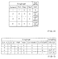
- the table in FIG. 14 shows an overview of possible states of the output signal hold of the process multiplexer 2.7 as a function of the input signals POR, flag1, flag2, SEL_1 and SEL_2.
- FIG. 14 shows a tabular overview of possible states of an output signal of a state decoder in a clock synchronization device according to the invention as a function of possible input values.
- a high logic level is denoted by “1” and a low logic level by “0".
- the reference character “X” indicates any logic level, that is, either “0” or “1”.
- "OR” stands for a logical OR operation. Illustrated in FIG. 14 are four states 1 to 4, each of which is distinguished by a specific combination of input signals, that is to say corresponding logical signal levels.
- State 1 is a reset state during which the device is reset.
- state 2 (run state), the device is in a normal operating state, that is, a request to switch the system clock is no longer valid or has been completed.
- Fig. 15 shows in tabular form the output of the clock gate (OR gate 2.8, Fig. 2) in response to the applied input signals.
- the entry "0" denotes a low logic level
- the entry "1” denotes a high logic level
- the entry "X” denotes an arbitrary logic level. Shown is the value of the output signal SYS_CLK as a function of values of the input signals CLK_A, CLK_B. POR, hold, ClkAGate2 and ClkBGate1.
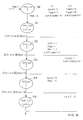
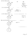
- FIG. 16 is a state diagram illustrating the flow of an embodiment of the method of the invention when the system clock is switched from a first to a second clock signal.
- FIG. 2 different states S1-S5 of the clock synchronization device 2 according to the invention (FIG. 2) are shown on the left in time sequence, which is symbolized by (vertical) arrows.
- respective outputs O1 and O2 of the first control module 2.5 and of the second control module 2.6 are shown on the right in FIG. 16, each above a horizontal line, that is to say the logic levels relevant output signals of the respective control modules listed.
- the designation "re” is shown in FIG. 16 - as in the following FIG.
- FIG. 17 shows a state diagram corresponding to FIG. 16 with states S6-S9 for switching the system clock from the (second) clock signal CLK_B back to the (first) clock signal CLK_A.
- states S6-S9 for switching the system clock from the (second) clock signal CLK_B back to the (first) clock signal CLK_A.
- the clock switching method according to the invention or the clock synchronization device according to the invention have a number of advantages over prior art methods or devices for asynchronous clock switching:
- the inventive Device is a fully digital implementation so that it can be synthesized without modification of standard logic libraries in hardware.
- the implementation of the present invention does not require any costly customization of circuit elements.
- the system clock period and / or frequency remains unchanged with the exception of a short transition time in which the system clock is switched over. Since the clock switching always takes place on a clock edge, there is no change in the duty cycle with the exception of the transition phase, which - as stated above - is always longer than 2.Tp + T s .
- the proposed optional safety logic avoids switching to a defective clock source or clock source whose clock period is longer than expected by retaining a switch request and maintaining the original clock.
Abstract
Description
Die vorliegende Erfindung betrifft ein Verfahren nach dem Oberbegriff des Patentanspruchs 1 zum Umschalten eines Systemtakts von einem ersten Taktsignal auf ein zweites Taktsignal, wobei der Umschaltvorgang durch ein Auswahl-Steuersignal ausgelöst wird und das Umschalten synchron zu dem ersten und/oder zweiten Taktsignal erfolgt.The present invention relates to a method according to the preamble of
Weiterhin betrifft die vorliegende Erfindung eine Taktsynchronisierungsvorrichtung für ein elektronisches System, insbesondere für einen Mikroprozessor, nach dem Oberbegriff des Patentanspruchs 6, aufweisend einen ersten Eingang für ein erstes Taktsignal, einen zweiten Eingang für ein zweites Taktsignal, einen dritten Eingang für ein Auswahl-Steuersignal und einen Ausgang für ein Systemtakt-Signal.Furthermore, the present invention relates to a clock synchronization device for an electronic system, in particular for a microprocessor, according to the preamble of
Darüber hinaus betrifft die vorliegende Erfindung eines Prozessoreinheit und eine Verwendung des erfindungsgemäßen Verfahrens.Moreover, the present invention relates to a processor unit and a use of the method according to the invention.
Zur Steuerung von elektronischen Systemen, wie insbesondere einer Prozessoreinheit in Form eines Mikroprozessors, ist es regelmäßig erforderlich, anwendungsspezifisch eine Auswahl aus einer Mehrzahl von extern angelegten asynchronen Taktsignalen zu treffen. Dabei kann je nach Anforderungsprofil ein regelmäßiges Umschalten zwischen unterschiedlichen Taktsignalen zur Ausgabe eines entsprechend veränderten System-Taktsignals erforderlich sein. Ein solcher Umschaltvorgang ist aber auch insbesondere dann erforderlich, wenn eines der externen Taktsignale fehlerhaft ist bzw. wenn eine entsprechende externe Taktsignal-Quelle vollständig ausfällt.For control of electronic systems, such as in particular a processor unit in the form of a microprocessor, it is regularly necessary to make an application-specific selection of a plurality of externally applied asynchronous clock signals. Depending on the requirement profile a regular switching between different clock signals to output a correspondingly changed system clock signal may be required. However, such a switching operation is also required in particular if one of the external clock signals is faulty or if a corresponding external clock signal source completely fails.
Aus der
Nachteilig an der vorstehend beschriebenen Schaltungsanordnung und dem bei ihrem Einsatz ausführbaren Verfahren ist, dass aufgrund der verwendeten analogen Schaltungselemente keine ausreichende Synthesefähigkeit mittels gängiger (Software-)Synthesewerkzeuge gegeben ist, zudem erfordert die zumindest teilweise analoge Ausgestaltung der vorhandenen asynchronen Zustandsmaschine einen hohen Aufwand bei der Herstellung, was sich in entsprechenden Kostennachteilen bemerkbar macht. Darüber hinaus können sich aufgrund der beschriebenen asynchronen Arbeitsweise beim Umschalten Taktverlängerungen und -verkürzungen ergeben, was sich negativ auf das Verhalten von durch das System-Taktsignal gesteuerten elektronischen Systemen, wie beispielsweise einen Mikroprozessor, auswirkt.A disadvantage of the circuit arrangement described above and executable in their use method is that due to the analog circuit elements used no sufficient synthesis capability by means of common (software) synthesis tools is given, also requires the at least partially analogous design of the existing asynchronous state machine high effort in the Production, which is reflected in corresponding cost disadvantages. In addition, due to the described asynchronous operation when switching clock extensions and shortenings result, which is negative on the behavior of controlled by the system clock signal electronic systems, such as a microprocessor affects.
Aus den Druckschriften
Der Erfindung liegt die Aufgabe zugrunde, unter Vermeidung der vorstehend aufgeführten Nachteile ein Verfahren und eine Vorrichtung der jeweils eingangs genannten Art dahingehend weiterzuentwickeln, dass diese ohne komplexe Anordnungen von Schaltungselementen, insbesondere analogen Schaltungselementen, auskommen, sodass insbesondere eine verbilligte Herstellung und eine verbesserte Synthesefähigkeit erreicht werden, wobei zudem während eines Umschaltvorgangs keine unerwünschten Taktverkürzungen oder -verlängerungen auftreten sollen. Außerdem soll eine möglichst unbeschränkte, flexible Einsetzbarkeit gewährleistet sein.The invention has for its object, while avoiding the disadvantages listed above, a method and an apparatus of the type mentioned in each case evolve to the effect that they do without complex arrangements of circuit elements, in particular analog circuit elements, so that in particular a cheaper production and improved synthesis capability In addition, during a switching operation, no unwanted clock shortening or prolongation should occur. In addition, the most unrestricted, flexible usability should be ensured.
Die Aufgabe wird bei einem Verfahren der eingangs genannten Art durch die kennzeichnenden Merkmale des Patentanspruchs 1 und bei einer Vorrichtung der eingangs genannten Art durch die kennzeichnenden Merkmale des Patentanspruchs 6 gelöst. Vorteilhafte Weiterbildungen des erfindungsgemäßen Verfahrens bzw. der erfindungsgemäßen Vorrichtung sind Gegenstand von Unteransprüchen.The object is achieved in a method of the type mentioned by the characterizing features of
Erfindungsgemäß ist ein Verfahren zum Umschalten eines Systemtakts von einem ersten Taktsignal auf ein zweites Taktsignal, wobei der Umschaltvorgang durch ein Auswahl-Steuersignal ausgelöst wird und das Umschalten synchron zu dem ersten und/oder zweiten Taktsignal erfolgt, dadurch gekennzeichnet, dass die Taktsteuerung von einer vorbestimmten Flanke des ersten Taktsignals auf eine entsprechende Flanke des zweiten Taktsignals übertragen wird, wobei ein Systemtakt-Signal nach Maßgabe des ersten Taktsignals auf einem ersten vorbestimmten logischen Signalpegel als Systemtakt-Haltesignal gehalten wird, wobei auf eine entsprechende Flanke des zweiten Taktsignals gewartet wird und wobei nach Maßgabe des zweiten Taktsignals das Systemtakt-Haltesignal auf einen zweiten logischen Zustand zurückgesetzt und zugleich das Systemtakt-Signal unter Verwendung des zweiten Taktsignals reaktiviert wird. Auf diese Weise wird der Systemtakt-Umschaltvorgang zwar durch das Auswahl-Steuersignal ausgelöst bzw. angestoßen, erfolgt jedoch anschließend vollständig nach Maßgabe der ersten und zweiten Taktsignale, die sich die Taktsteuerung gemäß dem vorstehend umrissenen Wechselspiel untereinander synchron übergeben.According to the invention, a method for switching a system clock from a first clock signal to a second clock signal, wherein the switching operation is triggered by a selection control signal and the switching occurs in synchronism with the first and / or second clock signal, characterized in that the clock control is transmitted from a predetermined edge of the first clock signal to a corresponding edge of the second clock signal, wherein a system clock signal after Assuming the first clock signal at a first predetermined logical signal level is held as a system clock hold signal, being waited for a corresponding edge of the second clock signal and wherein in accordance with the second clock signal, the system clock hold signal is reset to a second logic state and at the same time the system clock signal is reactivated using the second clock signal. In this way, although the system clock switching operation is triggered by the selection control signal, it is then fully executed in accordance with the first and second clock signals which synchronously transfer the clock timing to each other according to the interplay described above.
Entsprechend ist eine erfindungsgemäße Taktsynchronisierungsvorrichtung für ein elektronisches System, insbesondere für einen Mikroprozessor, aufweisend: einen ersten Eingang für ein erstes Taktsignal, einen zweiten Eingang für ein zweites Taktsignal, einen dritten Eingang für ein Auswahl-Steuersignal und einen Ausgang für ein Systemtakt-Signal, gekennzeichnet durch ein erstes Steuermodul, das durch das erste Taktsignal gesteuert ist und ein zweites Steuermodul, das durch das zweite Taktsignal gesteuert ist und das signaltechnisch mit dem ersten Steuermodul verbunden ist, wobei das erste Steuermodul bei Anliegen eines vorbestimmten Signalpegels des Auswahl-Steuersignals an dem dritten Eingang synchron mit dem ersten Taktsignal zum Setzen des Systemtakt-Signals von dem ersten Taktsignal auf einen vorbestimmten logischen Signalpegel als Systemtakt-Haltesignal ausgebildet ist und wobei das zweite Steuermodul synchron mit dem zweiten Taktsignal zum Zurücksetzen des Systemtakt-Haltesignals und zum Veranlassen einer Ausgabe des zweiten Taktsignals als Systemtakt-Signal ausgebildet ist.Accordingly, an electronic system clock synchronization device according to the invention, in particular for a microprocessor, has: a first input for a first clock signal, a second input for a second clock signal, a third input for a selection control signal and an output for a system clock signal, characterized by a first control module controlled by the first clock signal and a second control module controlled by the second clock signal and signal connected to the first control module, the first control module applying a predetermined signal level of the selection control signal to the first control module third input is formed in synchronism with the first clock signal for setting the system clock signal from the first clock signal to a predetermined logical signal level as a system clock hold signal and wherein the second control module synchronously with the second clock signal for resetting the system clock stop esignals and to Causing an output of the second clock signal is formed as a system clock signal.
Ein Grundgedanke der vorliegenden Erfindung ist somit, dass das Umschalten eines System-Taktsignals von einem ersten Taktsignal auf ein zweites Taktsignal synchron zu wenigstens einem der ersten und zweiten Taktsignale erfolgt, wodurch sich die eingangs erwähnten unerwünschten Taktverkürzungen und -verlängerungen vermeiden lassen. Die erfindungsgemäße Taktsynchronisierungsvorrichtung ist zum Durchführen eines derartigen synchronen Umschaltverfahrens derart ausgebildet, dass eine vollständig digitale Realisierung möglich ist, was zu der angestrebten Kostenreduzierung und verbesserten Synthesefähigkeit führt.A basic idea of the present invention is thus that the switching over of a system clock signal from a first clock signal to a second clock signal takes place in synchronism with at least one of the first and second clock signals, whereby the undesired clock shortenings and extensions mentioned in the introduction can be avoided. The clock synchronization device according to the invention is designed for carrying out such a synchronous switching method such that a completely digital realization is possible, which leads to the desired cost reduction and improved synthesis capability.
Im Zuge einer weiteren Ausgestaltung des erfindungsgemäßen Verfahrens ist vorgesehen, dass
- nach Maßgabe des Auswahl-Steuersignals durch ein erstes Steuermodul für das erste Taktsignal ein erstes Takt-Haltesignal synchron zu dem ersten Taktsignal erzeugt wird,
- das erste Takt-Haltesignal an ein zweites Steuermodul für das zweite Taktsignal weitergeleitet wird,
- durch das zweite Steuermodul ein zweites Takt-Haltesignal synchron zu dem zweiten Taktsignal erzeugt wird,
- aus den ersten und zweiten Taktsignalen das Sytemtakt-Haltesignal erzeugt wird,
- das zweite Takt-Haltesignal an das erste Steuermodul weitergeleitet wird und
- ein Zustand des ersten Takt-Haltesignals in Abhängigkeit von dem weitergeleiteten zweiten Takt-Haltesignal verändert wird.
- a first clock hold signal is generated in synchronism with the first clock signal according to the selection control signal by a first control module for the first clock signal,
- the first clock hold signal is forwarded to a second control module for the second clock signal,
- the second control module generates a second clock hold signal in synchronism with the second clock signal,
- the system clock hold signal is generated from the first and second clock signals,
- the second clock hold signal is forwarded to the first control module and
- a state of the first clock hold signal is changed in response to the forwarded second clock hold signal.
Auf diese Weise führen die ersten und zweiten Steuermodule im Rahmen einer Master-Slave-Abhängigkeit ein so genanntes Handshake-Verfahren durch, um sich in synchroner Weise gegenseitig über den ausgelösten Umschaltvorgang zu unterrichten und das Umschalten des Systemtakts vorzunehmen.In this way, the first and second control modules in the context of a master-slave dependency, a so-called handshake procedure in order to inform each other in a synchronous manner about the triggered switching process and to switch over the system clock.
Bei einer Weiterbildung der erfindungsgemäßen Taktsynchronisierungsvorrichtung ist zum Durchführen des weiter oben bereits erläuterten Handshake-Verfahrens vorgesehen, dass
- das erste Steuermodul nach Maßgabe des Auswahl-Steuersignals zum Erzeugen eines ersten Takt-Haltesignals und zum Weiterleiten desselben an das zweite Steuermodul ausgebildet ist,
- das zweite Steuermodul bei Empfang des ersten Takt-Haltesignals zum Erzeugen eines zweiten Takt-Haltesignals und zum Weiterleiten desselben an das erste Steuermodul ausgebildet ist,
- das erste Steuermodul zum Zurücksetzen des ersten Takt-Haltesignals bei Empfang des zweiten Takt-Haltesignals ausgebildet ist und
- das zweite Steuermodul zum Zurücksetzen des zweiten Takt-Haltesignals ausgebildet ist.
- the first control module is designed in accordance with the selection control signal for generating a first clock hold signal and for forwarding the same to the second control module,
- the second control module is formed on receipt of the first clock hold signal for generating a second clock hold signal and for forwarding the same to the first control module,
- the first control module is configured to reset the first clock hold signal upon receipt of the second clock hold signal, and
- the second control module is configured to reset the second clock hold signal.
Weiterhin ist zum Erzeugen des Systemtakt-Haltesignals bei einer anderen Weiterbildung der erfindungsgemäßen Taktsynchronisierungsvorrichtung ein Schaltungselement vorgesehen, das zum Erzeugen eines globalen Takt-Haltesignals als Vorläufer des Systemtakt-Haltesignals aus wenigstens den ersten und zweiten Takt-Haltesignalen ausgebildet ist. Das betreffende Schaltungselement kann dabei insbesondere als logisches OR-Gatter ausgebildet sein. Mit anderen Worten: durch das OR-Gatter wird ein Takt- Haltesignal aus einem ersten Zeitbereich (beispielsweise dem Bereich des ersten Taktsignals) in einen zweiten Zeitbereich (Bereich des zweiten Taktsignals) übergeben.Furthermore, in another development of the clock synchronization device according to the invention, a circuit element is provided for generating the system clock hold signal, which is designed to generate a global clock hold signal as a precursor of the system clock hold signal from at least the first and second clock hold signals. The relevant circuit element can be designed in particular as a logical OR gate. In other words, the OR gate transfers a clock hold signal from a first time range (for example, the range of the first clock signal) to a second time range (range of the second clock signal).
Optional kann dabei in Weiterbildung des erfindungsgemäßen Verfahrens vorgesehen sein, dass eine Zeit seit Anlegen des Auswahl-Steuersignals bestimmt wird und dass das Umschalten des Systemtakt-Signals bei Erreichen einer vorgegebenen Zeitschwelle freigegeben wird. Dabei kann die Zeitschwelle insbesondere durch einen Benutzer im Zuge einer softwaretechnischen Konfiguration eines zu steuernden Systems vorgegeben werden.Optionally, it can be provided in a development of the method according to the invention that a time has elapsed since the selection control signal was applied is determined and that the switching of the system clock signal is released upon reaching a predetermined time threshold. In this case, the time threshold can be specified in particular by a user in the course of a software-technical configuration of a system to be controlled.
Eine entsprechende Weiterbildung der erfindungsgemäßen Taktsynchronisierungsvorrichtung sieht vor, dass zumindest das erste Steuermodul einen Zähler aufweist, der zum Bestimmen einer Zeit in Abhängigkeit von dem Auswahl-Steuersignal ausgebildet ist.A corresponding development of the clock synchronization device according to the invention provides that at least the first control module has a counter which is designed to determine a time in dependence on the selection control signal.
In einem System, in dem der Ursprung einer Taktquelle nicht in einfacher Weise vorhersagbar beziehungsweise ermittelbar ist, kann es vorkommen, dass die Taktquelle beziehungsweise das entsprechende Taktsignal eines avisierten Umschaltvorgangs nicht länger verfügbar ist, da zum Beispiel die Eingangsleitung getrennt wurde, oder ein vollständiger Ausfall der Quelle vorliegt. Um das Umschalten auf einen ausgefallenen oder fehlerhaften Takt zu vermeiden, ist erfindungsgemäß vorgesehen, eine neue Taktquelle beziehungsweise einen neuen Takt, auf den umgeschaltet werden soll, zu erkennen und zu bestätigen, bevor die eigentliche Taktumschaltung erfolgt. Dies geschieht erfindungsgemäß durch das Einschalten oder Freigeben einer Sicherheitsfunktion (Timeout-Funktion).In a system in which the origin of a clock source is not easily predictable, it may happen that the clock source or the corresponding clock signal of an anticipated switching operation is no longer available, for example because the input line has been disconnected, or a complete failure the source is available. To avoid switching to a failed or faulty clock, the invention provides for a new clock source or a new clock to be switched to recognize and confirm before the actual clock switching takes place. This is done according to the invention by switching on or releasing a safety function (timeout function).
Die Sicherheits-/Timeout-Funktion ist ein einfacher Mechanismus, der nach einer vorbestimmten Abstast-Flanke, insbesondere einer steigenden Flanke, des neuen (System-)Taktsignals sucht, bevor der eigentliche Umschaltvorgang erfolgt, und der das Umschalten nur erlaubt, wenn die genannte vorbestimmte Flanke innerhalb eines vorbestimmten Zeitintervalls liegt, das durch einen entsprechenden Zähler überwacht wird. Der Zähler legt ein Zeitintervall fest, innerhalb dessen das Slave-Steuermodul ein durch das Master-Steuermodul zu bestätigendes Feedback-Takthaltesignal erzeugen kann. Wenn das Feedbacksignal nicht innerhalb der vorgesehenen Zeitempfangen wird, annulliert das Master-Steuermodul sein ursprünglich gesetztes Takt-Haltsignal, und der Taktumschaltungsvorgang wird abgebrochen.The safety / timeout function is a simple mechanism that looks for a predetermined skip edge, particularly a rising edge, of the new (system) clock signal before the actual switchover occurs, and that allows switching only when the named one predetermined edge within a predetermined time interval, which is monitored by a corresponding counter. The counter determines a time interval within which the slave control module will generate a feedback timing hold signal to be asserted by the master control module can. If the feedback signal is not received within the designated time, the master control module will cancel its originally set clock hold signal and the clock switching operation will be aborted.
Alternativ oder zusätzlich kann eine entsprechende Timeout-Logik auch als ein Mittel zum Erfassen und zur Steuerung eines Taktumschaltungs-Verzögerungsintervall eingesetzt werden, wobei die Takt-Umschaltungsverzögerung in Einheiten von Perioden des primären System-Taktsignals, das heißt desjenigen Taktsignals, das gegenwärtig als System-Taktsignal fungiert, bestimmt werden kann.Alternatively or additionally, a corresponding timeout logic may also be employed as a means for detecting and controlling a clock switching delay interval, wherein the clock switching delay is in units of periods of the primary system clock signal, that is, the clock signal currently used as system clock. Clock signal acts, can be determined.
Um ein versuchtes Umschalten des System-Taktsignals während eines gewissen Zeitraums, insbesondere vor dem optionalen Erreichen eines Zähler-Endwerts zu verhindern, ist im Zuge einer weiteren Ausgestaltung der erfindungsgemäßen Taktsynchronisierungsvorrichtung vorgesehen, dass zumindest das erste Steuermodul zum Erzeugen eines Taktumschaltungs-Sperrsignals in Abhängigkeit von dem Auswahl-Steuersignal ausgebildet ist, das zum Verhindern eines Zurücksetzens des Systemtakt-Haltesignals an das zweite Steuermodul angelegt ist.In order to prevent an attempted switching of the system clock signal during a certain period of time, in particular before the optional achievement of a counter end value, it is provided in the course of a further embodiment of the clock synchronization device according to the invention that at least the first control module for generating a clock switching inhibit signal as a function of is formed of the selection control signal, which is applied for preventing a resetting of the system clock hold signal to the second control module.
Darüber hinaus ist in Weiterbildung der erfindungsgemäßen Taktsynchronisierungsvorrichtung in vorteilhafter Weise vorgesehen, dass das erste Steuermodul zum Abschalten des Taktumschaltungs-Sperrsignals bei Erreichen einer vorgegebenen Zeitschwelle ausgebildet ist.In addition, it is advantageously provided in a further development of the clock synchronization device according to the invention that the first control module is designed to switch off the clock switching blocking signal when a predetermined time threshold is reached.
Vorzugsweise beträgt die Zeitschwelle mindestens 2·Ts, wobei Ts eine Periodendauer des zweiten Taktsignals (sekundäres Taktsignal) bezeichnet. Eine derartige Randbedingung ist insbesondere dann von Bedeutung, wenn die ersten und zweiten Taktsignale, zwischen denen umgeschaltet werden soll, eine deutlich voneinander abweichende Periodendauer besitzen, sodass durch eine entsprechende gewählte Zeitschwelle sichergestellt werden muss, dass innerhalb des so definierten Zeitfensters eine entsprechende Flanke des zweiten Taktsignals gefunden wird.Preferably, the time threshold is at least 2 * T s , where T s denotes a period of the second clock signal (secondary clock signal). Such a boundary condition is particularly important if the first and second clock signals to be switched between have a significantly different period, so that must be ensured by a corresponding selected time threshold that within the time window defined so a corresponding edge of the second clock signal is found.
Bei einer entsprechenden Weiterbildung der erfindungsgemäßen Taktsynchronisierungsvorrichtung ist vorgesehen, dass die Zeitschwelle durch einen Nutzer insbesondere softwaretechnisch vorgebbar ist, wobei die Zeitschwelle insbesondere mindestens 2·Ts beträgt, wobei Ts eine Periodendauer des zweiten Taktsignals bezeichnet.In a corresponding development of the clock synchronization device according to the invention, it is provided that the time threshold can be specified by a user, in particular by software technology, the time threshold in particular being at least 2 · T s , T s designating a period duration of the second clock signal.
Darüber hinaus kann optional vorgesehen sein, dass ein Umschaltvorgang ausgesetzt wird, wenn eine entsprechende Flanke des zweiten Taktsignals, auf die gewartet wird, gar nicht beziehungsweise nicht innerhalb eines vorbestimmten Zeitfensters kommt, was zum Beispiel auf eine ausgefallene Takt-Quelle hinweist. In diesem Zusammenhang wird der Umschaltbefehl gehalten und das bisherige (erste) Taktsignal als Systemtakt beibehalten. Vorrichtungstechnisch kann zu diesem Zweck insbesondere ein weiterer Zähler vorgesehen sein. Vorteilhafter Weise wird jedoch nur ein einziger Zähler zum Aktivieren des zweiten Taktsignals, wie verstehend beschrieben, und zum Vorgeben eines Zeitfensters für eine ausfallsichere Taktumschaltung eingesetzt.In addition, it can optionally be provided that a switching operation is suspended when a corresponding edge of the second clock signal being waited for does not arrive at all or not within a predetermined time window, which indicates, for example, a failed clock source. In this connection, the switching command is held and the previous (first) clock signal is maintained as a system clock. Device technology can be provided for this purpose, in particular a further counter. Advantageously, however, only a single counter is used to activate the second clock signal, as described above, and to specify a time window for a fail-safe clock switching.
Eine andere Weiterbildung des erfindungsgemäßen Verfahrens sieht vor, dass die ersten und zweiten Taktsignale jeweils aus einer Mehrzahl von Taktsignalen ausgewählt werden. Auf diese Weise ist eine optimal anwendungsspezifische Umschaltung von System-Taktsignalen möglich.Another development of the method according to the invention provides that the first and second clock signals are each selected from a plurality of clock signals. In this way, an optimal application-specific switching of system clock signals is possible.
In entsprechender Weiterbildung der erfindungsgemäßen Taktsynchronisierungsvorrichtung weist diese jeweils einen Multiplexer in Wirkverbindung mit den ersten und zweiten Eingängen auf, die zum Auswählen des ersten und zweiten Taktsignals aus jeweils einer Mehrzahl von Taktsignalen ausgebildet sind.In a corresponding development of the clock synchronization device according to the invention, the latter each has a multiplexer in operative connection with the first and second inputs, which are used to select the first and the second clock signal are each formed from a plurality of clock signals.
Die erfindungsgemäße Taktsynchronisierungsvorrichtung lässt sich in vorteilhafter Weise insbesondere in einer Prozessoreinheit, insbesondere in einem Mikroprozessor, zur Steuerung derselben einsetzen. Entsprechend ergibt sich eine bevorzugte Verwendung des erfindungsgemäßen Verfahrens zum Umschalten des Systemtakts bei einer Prozessoreinheit, insbesondere einem Mikroprozessor.The clock synchronization device according to the invention can advantageously be used in particular in a processor unit, in particular in a microprocessor, for controlling the same. Accordingly, there is a preferred use of the method according to the invention for switching the system clock in a processor unit, in particular a microprocessor.
Auf diese Weise schafft die vorliegende Erfindung im Rahmen der aufgeführten Ausgestaltungen eine Taktumschalt- bzw. -synchronisierungsvorrichtung, die in der Lage ist, in synchroner Weise von einer (ersten) Taktquelle auf eine andere (zweite) Taktquelle umzuschalten. Nach dem Vorstehenden besitzt die Vorrichtung hierzu grundsätzlich zunächst Mittel zum Auswählen einer neuen (zweiten) Taktquelle, deren Taktsignal als Systemtakt-Signal verwendet werden soll. Weiterhin hat die Vorrichtung asynchron arbeitende Mittel zum Abtasten eines Takteingangs, die unter Verwendung kreuzweise gekoppelter Synchronisierungsblöcke (Steuermodule) eine Anzahl von Steuer-/Statussignalen, insbesondere Takt-Haltesignale, generieren. Darüber hinaus besitzt die Vorrichtung Mittel zum asynchronen Abfragen der Steuersignale (Takt-Haltesignale), um aus diesen ein übergeordnetes globales Takt-Haltsignal zu erzeugen. Dieses stoppt - solange es aktiviert ist - den Systemtakt ("Einfrieren" des Systemtakts). Eine Takt-Umschaltverzögerung kann mittels eines internen Timers gesteuert werden. Darüber hinaus kann im Rahmen der vorliegenden Erfindung eine Fehlersicherung vorgesehen sein, die ein maßgebliches Merkmal des zweiten Taktsignals erkennt und danach entscheidet, ob ein Umschalten auf das neue (zweite) Taktsignal erfolgen soll.In this way, within the scope of the listed embodiments, the present invention provides a clock switching device capable of switching in a synchronous manner from one (first) clock source to another (second) clock source. In accordance with the foregoing, the apparatus basically has first means for selecting a new (second) clock source whose clock signal is to be used as the system clock signal. Furthermore, the apparatus has asynchronous means for sampling a clock input which, using cross-coupled sync blocks (control modules), generates a number of control / status signals, in particular clock hold signals. In addition, the device has means for asynchronously interrogating the control signals (clock hold signals) to generate from these a higher-level global clock stop signal. This stops - as long as it is activated - the system clock ("freezing" of the system clock). A clock switching delay can be controlled by means of an internal timer. In addition, in the context of the present invention, a fault protection can be provided, which detects a significant feature of the second clock signal and then decides whether switching to the new (second) clock signal should occur.
Weitere Eigenschaften und Vorteile der vorliegenden Erfindung ergeben sich aus der nachfolgenden Beschreibung eines Ausführungsbeispiels anhand der Zeichnung. Es zeigt/zeigen:
- Fig. 1
- ein schematisches Blockschaltbild einer Schaltungsanordnung mit einer erfindungsgemäßen Taktsynchronisierungsvorrichtung für ein elektronisches System bei Verwendung mit bzw. in einem Mikroprozessor;
- Fig. 2
- ein detailliertes Blockschaltbild einer ersten Ausgestaltung der erfindungsgemäßen Taktsynchronisierungsvorrichtung;
- Fig. 3
- ein detailliertes Blockschaltbild eines ersten Steuermoduls der Taktsynchronisierungsvorrichtung gemäß Fig. 2;
- Fig. 4a-d:
- logische Schaltdiagramme zur Darstellung der Erzeugung von Steuersignalen in einem Steuerblock gemäß Fig. 3;
- Fig. 5:
- ein logisches Schaltdiagramm zur Darstellung der Erzeugung eines Zähler-Freigabesignals in Fig. 3;
- Fig. 6:
- detailliert einen Schaltungsaufbau zum Erzeugen eines Takt-Haltesignals;
- Fig. 7:
- detailliert eine Schaltungsanordnung zum Erzeugen eines Taktumschaltungs-Sperrsignals;
- Fig. 8:
- detailliert eine Schaltungsanordnung zum Erzeugen eines Gattersignals;
- Fig. 9:
- detailliert eine Schaltungsanordnung zum Erzeugen eines ersten Auswahlsignals;
- Fig. 10:
- detailliert eine logische Schaltungsanordnung eines Taktgatters gemäß Fig. 2;
- Fig. 11:
- detailliert eine Schaltungsanordnung zum Erzeugen eines Zählersignals;
- Fig. 12:
- detailliert eine Schaltungsanordnung zum Erzeugen eines globalen Takt-Haltesignals;
- Fig. 13a,b
- ein Zeitablauf-Diagramm zur Erläuterung eines Betriebs der erfindungsgemäßen Taktsynchronisierungsvorrichtung bzw. zur Darstellung eines erfindungsgemäßen Verfahrens zum Umschalten eines Systemtakts;
- Fig. 14:
- eine tabellarische Übersicht möglicher Zustände eines Ausgangssignals eines Zustandsdekodierers in einer erfindungsgemäßen Taktsynchronisierungsvorrichtung in Abhängigkeit von möglichen Eingangswerten;
- Fig. 15:
- in tabellarischer Form die Ausgabe des Takt-Gatters in Fig. 2in Abhängigkeit von anliegenden Eingangssignalen;
- Fig. 16:
- ein Zustandsdiagramm zur Darstellung des Ablaufs einer Ausgestaltung des erfindungsgemäßen Verfahrens beim Umschalten des Systemtakts von einem ersten auf ein zweites Taktsignal; und
- Fig. 17
- ein der Fig. 16 entsprechendes Zustandsdiagramm für ein Umschalten des Systemtakts von dem zweiten Taktsignal zurück auf das erste Taktsignal.
- Fig. 1
- a schematic block diagram of a circuit arrangement with a clock synchronization device according to the invention for an electronic system when used with or in a microprocessor;
- Fig. 2
- a detailed block diagram of a first embodiment of the clock synchronization device according to the invention;
- Fig. 3
- a detailed block diagram of a first control module of the clock synchronization device of FIG. 2;
- Fig. 4a-d:
- logical circuit diagrams for illustrating the generation of control signals in a control block of FIG. 3;
- Fig. 5:
- a logic circuit diagram illustrating the generation of a counter enable signal in Fig. 3;
- Fig. 6:
- detail a circuit construction for generating a clock hold signal;
- Fig. 7:
- in detail, a circuit arrangement for generating a clock switching inhibit signal;
- Fig. 8:
- in detail, a circuit arrangement for generating a gate signal;
- Fig. 9:
- in detail, a circuit arrangement for generating a first selection signal;
- Fig. 10:
- in detail, a logical circuit arrangement of a clock gate of FIG. 2;
- Fig. 11:
- in detail, a circuit arrangement for generating a counter signal;
- Fig. 12:
- in detail, a circuit arrangement for generating a global clock hold signal;
- Fig. 13a, b
- a timing diagram for explaining an operation of the clock synchronization device according to the invention or for illustrating a method according to the invention for switching a system clock;
- Fig. 14:
- a tabular overview of possible states of an output signal of a state decoder in a clock synchronization device according to the invention as a function of possible input values;
- Fig. 15:
- in tabular form, the output of the clock gate in Figure 2 in response to applied input signals;
- Fig. 16:
- a state diagram for illustrating the sequence of an embodiment of the method according to the invention when switching the system clock from a first to a second clock signal; and
- Fig. 17
- a corresponding to Fig. 16 state diagram for switching the system clock from the second clock signal back to the first clock signal.
Fig. 1 zeigt anhand eines schematischen Blockschaltbilds eine Ausgestaltung einer Schaltungsanordnung 1, die unter anderem eine erfindungsgemäße Taktsynchronisierungsvorrichtung 2 aufweist und die zur Verwendung mit einer Prozessoreinheit, wie einem Mikroprozessor 3, vorgesehen ist. Abweichend von der Darstellung in Fig. 1 kann die Schaltungsanordnung 1 mit der erfindungsgemäßen Taktsynchronisierungsvorrichtung 2 auch in die Prozessoreinheit 3 integriert sein.1 shows by way of a schematic block diagram an embodiment of a
Zusätzlich zu der bereits erwähnten Taktsynchronisierungsvorrichtung 2 weist die Schaltungsanordnung 1 gemäß Fig. 1 einen ersten Multiplexer 4 und einen zweiten Multiplexer 5 auf, die mit der Taktsynchronisierungsvorrichtung 2 in signaltechnischer Wirkverbindung stehen. Der erste Multiplexer 4 besitzt n Eingänge für externe Taktsignale CLK_1, CLK_2, ..., CLK_n, und der zweite Multiplexer 5 besitzt ebenfalls n Eingänge für externe Taktsignale CLK_1, CLK_2, ..., CLK_n. Weiterhin weist die Schaltungsanordnung 1 gemäß Fig. 1 eine Steuereinheit 6 auf, die sowohl mit den ersten und zweiten Multiplexern 4, 5 als auch mit der Taktsynchronisierungsvorrichtung 2 in signaltechnischer Wirkverbindung steht. Zumindest an der Taktsynchronisierungsvorrichtung 2 ist darüber hinaus ein weiterer Eingang POR für ein Reset-Signal (Power-on Reset) vorgesehen. Die Taktsynchronisierungsvorrichtung 2 hat einen ersten Eingang 2.1, einen zweiten Eingang 2.2 sowie einen dritten Eingang 2.3. Darüber hinaus weist die Taktsynchronisierungsvorrichtung 2 einen Ausgang 2.4 auf, sowie weitere Anschlüsse für eine Versorgungsspannung VDD, ein Referenzpotential (Erde beziehungsweise Masse) GND und für (Nutzer-) Eingabewerte TVAL1, TVAL2, auf die später noch eingegangen wird.In addition to the already mentioned
An der Steuereinheit 6 liegen ein erstes Steuersignal CLK_SEL[n:1] und ein zweites Steuersignal SW an. Das erste Steuersignal CLK_SEL[n:1] wird von der Prozessoreinheit 3 oder - abweichend von der Ausgestaltung der Fig. 1 - von einer weiteren externen Einheit (nicht gezeigt) geliefert und kann bezogen auf die Taktsignale CLK_1, CLK_2, ..., CLK_n asynchron sein. Das zweite (externe) Steuersignal SW aktiviert ggf. die Veranlassung einer Taktumschaltung auf das durch das erste Steuersignal CLK_SEL[n:1] bestimmte Taktsignal CLK_1, CLK_2,..., CLK_n.At the
An dem ersten Eingang 2.1 der Taktsynchronisierungsvorrichtung 2 liegt ein erstes Taktsignal CLK_A an, das von dem ersten Multiplexer 4 nach Maßgabe der Steuereinheit 6 aus der extern vorgegebenen Anzahl von Taktsignalen CLK_1, ..., CLK_n ausgewählt wurde. Entsprechend liegt am Eingang 2.2 der Taktsynchronisierungsvorrichtung 2 ein anderes, zweites Taktsignal CLK_B, das von dem zweiten Multiplexer 5 nach Maßgabe der Steuereinheit 6 aus der extern vorgegebenen Anzahl von Steuersignalen CLK_1, ..., CLK_n ausgewählt wurde und das zu dem ersten Taktsignal asynchron ist. An dem dritten Eingang 2.3 der Taktsynchronisierungsvorrichtung 2 liegt ein von der Steuereinheit 6 bereitgestelltes Umschaltsignal oder Auswahl-Steuersignal SEL an, welches einen Umschaltvorgang zum erfindungsgemäßen Umschalten eines Systemtaktes auslöst, wie nachfolgend noch detaillierter beschrieben wird. Am Ausgang 2.4 wird durch die Taktsynchronisierungsvorrichtung 2 ein Systemtakt-Signal SYS_CLK an die Prozessoreinheit 3 ausgegeben, wobei es sich bei dem Systemtakt-Signal SYS_CLK auch um ein Systemtakt-Haltesignal handeln kann, wie nachfolgend ebenfalls noch detailliert beschrieben wird.At the first input 2.1 of the
Der durch die Steuereinheit 6 mittels des Auswahl-Steuersignals SEL ausgelöste Umschaltvorgang kann insbesondere durch Fehlerhaftigkeit oder vollständigen Ausfall eines gegenwärtigen Systemtaktgebers (clock) oder willkürlich durch entsprechende Eingabe, beispielsweise durch einen Benutzer, veranlasst sein, was dem Fachmann bekannt ist.The switching operation triggered by the
Fig. 2 zeigt anhand eines detaillierteren Blockschaltbilds eine erfindungsgemäße Ausgestaltung der Taktsynchronisierungsvorrichtung 2 gemäß Fig. 1. Gleiche bzw. gleich wirkende Elemente sind dabei mit denselben Bezugszeichen wie in Fig. 1 versehen.2 shows, on the basis of a more detailed block diagram, an embodiment according to the invention of the
Die Taktsynchronisierungsvorrichtung 2 besitzt gemäß Fig. 2 zwei strukturell identisch ausgebildete Steuermodule, nämlich ein erstes Steuermodul (Synchronisierer) 2.5 und ein zweites Steuermodul (Synchronisierer) 2.6. Darüber hinaus weist die Taktsynchronisierungsvorrichtung 2 noch zwei weitere Schaltungselemente in Form eines Prozessmultiplexers (Synchronisierungszustand-Dekodierer) 2.7 und eines logischen Verknüpfungselements (Takt-Gatter) 2.8 auf, wobei letzteres vorliegend als OR-Gatter ausgebildet ist.According to FIG. 2, the
Das erste Steuermodul 2.5 ist mit Eingang 2.1 der Taktsynchronisierungsvorrichtung 2 verbunden, sodass an ihm das erste Taktsignal CLK_A anliegt. Das zweite Steuermodul 2.6 ist mit dem Eingang 2.2 der Taktsynchronisierungsvorrichtung 2 verbunden, sodass an ihm das zweite Taktsignal CLK_B anliegt. Das Umschaltsignal bzw. Auswahl-Steuersignal SEL liegt sowohl an dem ersten Steuermodul 2.5 als auch an dem zweiten Steuermodul 2.6 an. Beide Steuermodule 2.5, 2.6 besitzen darüber hinaus einen Eingang für das Reset-Signal POR. Bei dem gezeigten Ausführungsbeispiel ist zudem für jedes Steuermodul ein Zählerelement TVAL1 beziehungsweise TVAL2, das heißt ein entsprechendes Zeitintervall vorgebbar (vergleiche Fig. 1), worauf später noch genauer eingegangen wird.The first control module 2.5 is connected to input 2.1 of the
Gemäß der Darstellung in Fig. 2 ist das Steuermodul 2.5 zum Ausgeben eines Taktumschaltungs-Sperrsignals flag1 ausgebildet; entsprechend ist das Steuermodul zum Ausgeben eines Taktumschaltungs-Sperrsignals flag2 ausgebildet. Weiterhin sind die Steuermodul 2.5, 2.6 jeweils zum Ausgeben eines Gattersignals ClkBGate1 bzw. ClkAGate2 ausgebildet. Weiterhin sind die Steuermodule 2.5, 2.6 jeweils zum Ausgeben eines Takt-Haltesignals hold1 bzw. hold2 und zum Ausgeben eines ersten beziehungsweise eines zweiten Auswahlsignals SEL_1 beziehungsweise SEL_2 ausgebildet.As shown in Fig. 2, the control module 2.5 is configured to output a clock switching inhibit signal flag1; Accordingly, the control module is configured to output a clock switching inhibit signal flag2. Furthermore, the control modules 2.5, 2.6 are each designed to output a gate signal ClkBGate1 or ClkAGate2. Furthermore, the control modules 2.5, 2.6 are each designed to output a clock hold signal hold1 or hold2 and to output a first or a second selection signal SEL_1 or SEL_2.
Die meisten der vorstehend aufgeführten Ausgabesignale, das heißt die Ausgabesignale SEL_1, SEL_2, hold1, hold2, flag1, flag2 der ersten und zweiten Steuermodule 2.5, 2.6 liegen an entsprechenden Eingängen des Prozessmultiplexers 2.7 an, wie in Fig. 2 dargestellt. Darüber hinaus liegt das Taktumschaltungs-Sperrsignal flag1 des ersten Steuermoduls 2.5 sowie das Takt-Haltesignal hold des ersten Steuermoduls 2.5 an entsprechenden weiteren Eingängen des zweiten Steuermoduls 2.6 an, wie ebenfalls in Fig. 2 dargestellt. Entsprechend liegen das Taktumschaltungs-Sperrsignal flag2 und das Takt-Haltesignal hold2 des zweiten Steuermoduls 2.6 an entsprechenden weiteren Eingängen des ersten Steuermoduls 2.5 an, sodass die Steuermodule 2.5, 2.6 miteinander gekoppelt sind.Most of the output signals listed above, that is the output signals SEL_1, SEL_2, hold1, hold2, flag1, flag2 of the first and second control modules 2.5, 2.6 are applied to corresponding inputs of the process multiplexer 2.7, as shown in Fig. 2. In addition, the clock switching inhibit signal flag1 of the first control module 2.5 and the clock hold signal hold of the first control module 2.5 is applied to corresponding further inputs of the second control module 2.6, as also shown in FIG. Accordingly, the clock switching inhibit signal flag2 and the clock hold signal hold2 of the second control module 2.6 are applied to corresponding further inputs of the first control module 2.5, so that the control modules 2.5, 2.6 are coupled together.
Die Ausgabesignale ClkBGate1 und ClkAGate2 liegen an dem Takt-Gatter 2.8 an.The output signals ClkBGate1 and ClkAGate2 are applied to the clock gate 2.8.
Der Prozessmultiplexer 2.7 erzeugt aus seinen Eingangssignalen, zu denen weiterhin gemäß Fig. 2 das Reset-Signal POR gehört, als Ausgangssignale ein verzögertes Auswahlsignal SEL_del und ein Haltesignal hold. Erstes bildet zusammen mit dem Reset-Signal POR und den bereits erwähnten Gattersignalen CIkBGate1, ClkAGate2 sowie den ersten und zweiten Taktsignalen CLK-A, CLK_B die Eingangssignale für das OR-Gatter (Takt-Gatter) 2.8, welches daraus an seinem Ausgang bzw. dem Ausgang 2.4 der erfindungsgemäßen Taktsynchronisierungsvorrichtung 2 das Systemtakt-Signal SYS_CLK ausgibt.The process multiplexer 2.7 generates from its input signals, to which furthermore the reset signal POR belongs according to FIG. 2, as output signals a delayed selection signal SEL_del and a hold signal hold. The first forms, together with the reset signal POR and the already mentioned gate signals CIkBGate1, ClkAGate2 and the first and second clock signals CLK-A, CLK_B, the input signals for the OR gate (clock gate) 2.8, which outputs from it at its output or the output 2.4 of the
Fig. 3 ist ein detailliertes Blockschaltbild eines ersten Steuermoduls der Taktsynchronisierungsvorrichtung gemäß Fig. 2 und 3 zeigt eine detailliertere Darstellung des ersten Steuermoduls 2.5. Es sei betont, dass das zweite Steuermodul 2.6 strukturell identisch aufgebaut ist, sodass vorliegend auf eine ebenso detaillierte Beschreibung desselben verzichtet werden kann.3 is a detailed block diagram of a first control module of the clock synchronization device of FIG. 2 and FIG. 3 shows a more detailed illustration of the first control module 2.5. It should be emphasized that the second control module 2.6 is constructed structurally identical, so that in the present case an equally detailed description of the same can be dispensed with.
Das erste Steuermodul 2.5 und entsprechend das zweite Steuermodul 2.6 (hier nicht gezeigt) beinhaltet einen Steuerblock 2.5a, sowie eine Zustandsmaschine 2.5a', die wiederum einen Zähler 2.5b, eine Haltesignal-Steuereinheit 2.5c, eine Sperrsignal-Steuereinheit 2.5d sowie eine Gatter-Steuereinheit 2.5e, aufweist.The first control module 2.5 and correspondingly the second control module 2.6 (not shown here) includes a control block 2.5a, and a state machine 2.5a ', which in turn a counter 2.5b, a holding signal control unit 2.5c, a blocking signal control unit 2.5d and a Gate control unit 2.5e, has.
Des Weiteren besitzt die Zustandsmaschine 2.5a' eine Auswahl-Steuereinheit 2.5f sowie eine Zähler-Steuereinheit 2.5h und zwei Vergleicher 2.5i, 2.5j.Furthermore, the state machine 2.5a 'has a selection control unit 2.5f and a counter control unit 2.5h and two comparators 2.5i, 2.5j.
An dem Steuerblock 2.5a des ersten Steuermoduls 2.5 liegt das von dem zweiten Steuermodul (nicht gezeigt) erzeugte Taktumschaltungs-Sperrsignal flag2, das ebenfalls von dem zweiten Steuermodul erzeugte Takt- Haltesignal hold2 sowie das Umschaltsignal SEL an. Weiterhin liegen an dem Steuerblock 2.5a das intern, das heißt innerhalb des dargestellten ersten Steuermoduls 2.5 erzeugte Taktumschaltungs-Sperrsignal flag1, das Gattersignal ClkBGate1 sowie das Auswahlsignal SEL_1 an.At the control block 2.5a of the first control module 2.5 of the second control module (not shown) generated clock switching inhibit signal flag2, which is also generated by the second control module clock hold signal hold2 and the switching signal SEL on. Furthermore, the control block 2.5a has the clock switching inhibit signal flag1 generated internally, that is to say within the illustrated first control module 2.5, the gate signal ClkBGate1 and the selection signal SEL_1.
Der Steuerblock 2.5 gibt die Steuersignale ASST, CDET, REQD und CNTST aus, auf die später noch detailliert eingegangen wird. Die vorstehend genannten Steuersignale des Steuerblocks 2.5a liegen an der Zustandsmaschine 2.5a' an, wie in Fig. 3 gezeigt.The control block 2.5 outputs the control signals ASST, CDET, REQD and CNTST, which will be discussed in detail later. The above Control signals of the control block 2.5a mentioned are applied to the state machine 2.5a ', as shown in Fig. 3.
In der Zustandsmaschine 2.5a' erzeugt der Zähler 2.5b ein Zählersignal beziehungsweise einen Zählerwert cnt1, der über eine Acht-Bit-Leitung 2.5k sowohl an die Haltesignal-Steuereinheit 2.5c und die Sperrsignal-Steuereinheit 2.5d als auch an die Vergleicher 2.5i, 2.5j geliefert wird.In the state machine 2.5a ', the counter 2.5b generates a counter signal or a counter value cnt1, which via an eight-bit line 2.5k both to the holding signal control unit 2.5c and the blocking signal control unit 2.5d and to the comparator 2.5i , 2.5j is delivered.
Die Haltesignal-Steuereinheit 2.5c erzeugt das Takt-Haltesignal hold1. Die Sperrsignal-Steuereinheit 2.5d erzeugt das Takt-Umschaltungs-Sperrsignal flag1. Die Gatter-Steuereinheit 2.5e erzeugt das Gattersignal ClkBGate1. Die Auswahl-Steuereinheit 2.5f erzeugt das Auswahlsignal SEL_1. Die Zähler-Steuereinheit 2.5h erzeugt ein Zähler-Freigabesignal CNTEN.The hold signal control unit 2.5c generates the clock hold signal hold1. The inhibit signal control unit 2.5d generates the clock switching inhibit signal flag1. The gate control unit 2.5e generates the gate signal ClkBGate1. The selection control unit 2.5f generates the selection signal SEL_1. The counter control unit 2.5h generates a counter enable signal CNTEN.
Des Weiteren liegt an allen Steuereinheiten 2.5c-2.5f mit Ausnahme der Zähler-Steuereinheit 2.5h sowie an dem Zähler 2.5b sowohl das erste Taktsignal CLK_A als auch das Reset-Signal POR an.Furthermore, all the control units 2.5c-2.5f except for the counter control unit 2.5h and the counter 2.5b have both the first clock signal CLK_A and the reset signal POR on.
Die Vergleicher 2.5i, 2.5j stehen mit der Zähler-Steuereinheit 2.5h in signaltechnischer Wirkverbindung. Darüber hinaus liegt an der Auswahl-Steuereinheit 2.5f das Umschaltsignal SEL sowie das Auswahlsignal SEL_1 an. Fig. 4a-d zeigen logische Schaltdiagramme zur Darstellung der Erzeugung von Steuersignalen in einem Steuerblock gemäß Fig. 3.The comparators 2.5i, 2.5j are in operative connection with the counter control unit 2.5h. In addition, the switching control signal SEL and the selection signal SEL_1 are applied to the selection control unit 2.5f. 4a-d show logic circuit diagrams for illustrating the generation of control signals in a control block according to FIG. 3.
Gemäß Fig. 4a sind die Signale flag2 und hold2 zur Erzeugung des Steuersignals ASST mittels eines logischen UND-Glieds verknüpft, das heißt, das Steuersignal ASST besitzt den Wert "1" (hoher Logikpegel), wenn sowohl das Taktumschaltungs-Sperrsignal flag2 als auch das Takt-Haltesignal hold2 einen hohen Logikpegel hat.According to Fig. 4a, the signals flag2 and hold2 for generating the control signal ASST are linked by means of a logical AND gate, that is, the control signal ASST has the value "1" (high logic level) when both the clock switching inhibit signal flag2 and the Clock hold signal hold2 has a high logic level.
Gemäß Fig. 4b wird das Steuersignal CDET erzeugt, indem das Takt- Haltesignal hold1 in invertierter Form über ein logisches UND-Glied mit dem Ausgang eines exklusiven ODER-Glieds verknüpft wird, wobei an den Eingängen des exklusiven ODER-Glieds das Auswahlsignal SEL beziehungsweise das Auswahlsignal SEL_1 anliegen. Auf diese Weise besitzt das Steuersignal CDET einen hohen Logikpegel, wenn entweder das Auswahlsignal SEL oder das Auswahlsignal SEL_1 einen hohen Logikpegel besitzt und sogleich das Takt-Haltesignal hold1 einen niedrigen Logikpegel hat.According to Fig. 4b, the control signal CDET is generated by the clock hold signal hold1 is connected in an inverted form via a logical AND gate to the output of an exclusive OR gate, wherein at the inputs of the exclusive OR gate, the selection signal SEL or Selection signal SEL_1 abut. In this way, the control signal CDET has a high logic level when either the selection signal SEL or the selection signal SEL_1 has a high logic level and immediately the clock hold signal hold1 has a low logic level.
Gemäß Fig. 4c wird das Steuersignal REQD erzeugt, indem das Auswahlsignal SEL_1 über ein logisches UND-Glied mit dem invertierten Taktumschaltungs-Sperrsignal flag1 verknüpft wird. Auf diese Weise hat das Steuersignal REQD einen hohen Logikpegel, wenn das Auswahlsignal SEL_1 einen hohen Logikpegel und das Taktumschaltungs-Sperrsignal flag1 einen niedrigen Logikpegel hat.According to FIG. 4c, the control signal REQD is generated by linking the selection signal SEL_1 via a logical AND gate to the inverted clock switching inhibit signal flag1. In this way, the control signal REQD has a high logic level when the selection signal SEL_1 has a high logic level and the clock switching inhibit signal flag1 has a low logic level.
Gemäß Fig. 4d wird das Steuersignal CNTST durch eine logische UND-Verknüpfung des Auswahlsignals SEL_1 und des Gattersignals ClkBGate1 erzeugt. Auf diese Weise hat das Steuersignal CNTST einen hohen Logikpegel, wenn sowohl das Auswahlsignal SEL_1 als auch das Gattersignal ClkBGate1 einen hohen Logikpegel besitzen.According to Fig. 4d, the control signal CNTST is generated by a logical AND operation of the selection signal SEL_1 and the gate signal ClkBGate1. In this way, the control signal CNTST has a high logic level when both the selection signal SEL_1 and the gate signal ClkBGate1 have a high logic level.
Die Logikschaltungen der Fig. 4a-d ergeben zusammen denSteuerblock 2.5a gemäß Fig. 3.The logic circuits of Figures 4a-d together form the control block 2.5a of Figure 3.
Fig. 5 zeigt detailliert eine logische Schaltungsanordnung der Zähler-Steuereinheit 2.5h in Fig. 2. Gemäß Fig. 5 wird das Zähler-Freigabesignal CNTEN erzeugt, indem zunächst das Takt-Haltesignal hold1 mit einem Signal A logisch UND-verknüpft wird. Dabei stellt das Signal A eine Ausgabe des Vergleichers 2.5i dar, der den Zählerwert cnt1 des Zählers 2.5b mit dem vorgegebenen Endwert TVAL1 (vergleiche Fig. 1, 2) vergleicht und einen hohen Logikpegel ausgibt, wenn gilt: cnt1 ≤TVAL1. Weiterhin wird das Signal A mit einem weiteren Signal B logisch UND-verknüpft, wobei das Signal B einen hohen Logikpegel besitzt, wenn gilt: cnt1 = "00000001". Die Ergebnisse der vorstehend erläuterten logischen UND-Verknüpfungen in Fig. 5 werden anschließend logisch ODER-verknüpft, sodass das Zähler-Freigabesignal CNTEN einen hohen Logikpegel besitzt, wenn entweder die UND-Verknüpfung der Signale hold1 und A oder die UND-Verknüpfung der Signale A und B einen hohen Logikpegel ergibt.Fig. 5 shows in detail a logical circuit arrangement of the counter control unit 2.5h in Fig. 2. Referring to Fig. 5, the counter enable signal CNTEN is generated by first logically ANDing the clock hold signal hold1 with a signal A. In this case, the signal A represents an output of the comparator 2.5i, which compares the counter value cnt1 of the counter 2.5b with the predetermined end value TVAL1 (cf. FIGS. 1, 2) and a comparator high logic level if: cnt1 ≤TVAL1. Furthermore, the signal A is logically ANDed with another signal B, the signal B having a high logic level, if: cnt1 = "00000001". The results of the above-explained logical AND operations in Fig. 5 are then logically ORed so that the counter enable signal CNTEN has a high logic level when either the AND of the signals hold1 and A or the AND of the signals A and B gives a high logic level.
Die zu den Fig. 4a-d und 5 gebrachten Ausführungen gelten entsprechend für das zweite Sperrmodul 2.6 (Fig. 1, 2) wenn die jeweiligen Signale, insbesondere Signale hold 1, flag1, hold2, flag2, cnt1, TVAL1, SEL_1 und ClkBGate1 durch die entsprechenden Signale für das zweite Steuermodul 2.6 ersetzt werden (vergleiche Fig. 2).The statements made with reference to FIGS. 4a-d and 5 apply correspondingly to the second blocking module 2.6 (FIGS. 1, 2) when the respective signals, in particular signals hold1, flag1, hold2, flag2, cnt1, TVAL1, SEL_1 and ClkBGate1, pass through the corresponding signals for the second control module 2.6 are replaced (see FIG. 2).
Fig. 6 zeigt detailliert einen Schaltungsaufbau zum Erzeugen eines Takt-Haltesignals. Dargestellt ist insbesondere ein Schaltungsaufbau der Halte-signal-Steuereinheit 2.5c (Fig. 3). Die in Fig. 6 dargestellte Schaltungsanordnung ist im Wesentlichen aus einer Abfolge von 2-zu-1-Multiplexern MUX1-MUX7 gebildet. Diese fungieren als Wechselschalter, die nach Maßgabe eines jeweils angelegten Steuer- oder Adresssignals zwischen ihren beiden jeweiligen Eingängen umschalten. Dabei wird je nach Logikpegel des Adresssignals entweder das am den mit "0" bezeichneten Eingang des Multiplexers anliegende Signal (niedriger Logikpegel des Adresssignals) oder das an dem mit "1" bezeichneten Eingang des Multiplexers anliegende Signal (hoher Logikpegel des Adresssignals) ausgegeben. Im Folgenden wird der "0" bezeichnete Eingang der Multiplexer MUXi auch mit E0 und der mit "1" bezeichnete jeweilige Eingang der Multiplexer MUXi mit E1 bezeichnet.Fig. 6 shows in detail a circuit construction for generating a clock hold signal. Shown is in particular a circuit structure of the holding signal control unit 2.5c (Fig. 3). The circuit arrangement illustrated in FIG. 6 is essentially formed from a sequence of 2-to-1 multiplexers MUX1-MUX7. These act as a changeover switch, which switch in accordance with a respectively applied control or address signal between their two respective inputs. Depending on the logic level of the address signal, either the signal present at the input of the multiplexer designated as "0" (low logic level of the address signal) or the signal present at the input of the multiplexer designated "1" (high logic level of the address signal) is output. Hereinafter, the input of the multiplexer MUXi designated "0" is also denoted by E0 and the respective input of the multiplexer MUXi denoted by "1" is denoted by E1.
An dem ersten Multiplexer MUX1 liegt bei E0 das Takt-Haltesignal hold1 an, während E1 auf Massepotential GND liegt. Das Adresssignal für MUX1 wird durch eine logische UND-Verknüpfung von Signalen C, D erzeugt, wobei C den Zählerwert cnt1 und D den eingestellten Zählerendwert TVAL1 bezeichnen. Der Ausgang des Multiplexers MUX1 ist mit dem Eingang E1 des Multiplexers MUX2 verbunden. Am Eingang E0 des Multiplexers MUX2 liegt wiederum das Takt-Haltesignal hold1 an. Das Adresssignal für den Multiplexer MUX2 wird durch das Steuersignal CNTEN (vergleiche Fig. 3, 5) gebildet. Der Ausgang des Multiplexers MUX2 ist mit dem Eingang E1 des Multiplexers MUX3 verbunden, während an dem Eingang E0 des Multiplexers MUX3 wiederum das Takt-Haltesignal hold 1 anliegt. Das Adresssignal für den Multiplexer MUX3 wird durch das Steuersignal CNTST (vergleiche Fig. 3, 4d) gebildet. Der Ausgang des Multiplexers MUX3 ist mit dem Eingang E0 des Multiplexers MUX4 verbunden, an dessen Eingang E1 das Spannungsversorgungs-Signal VDD anliegt. Das Adresssignal für den Multiplexer MUX4 wird durch das Steuersignal REQD (vergleiche Fig. 3, 4c) gebildet. Der Ausgang des Multiplexers MUX4 ist mit dem Eingang E0 des Multiplexers MUX6 verbunden. Der Eingang E1 des Multiplexers MUX6 ist mit dem Ausgang des Multiplexers MUX5 verbunden, an dessen Eingang E0 das Takt-Haltesignal hold1 und an dessen Eingang E1 wiederum das Spannungsversorgungs-Signal VDD anliegt. Das Adresssignal für den Multiplexer MUX5 wird gebildet durch eine logische UND-Verknüpfung des invertierten Takt-Haltesignals hold2 (vergleiche Fig. 2) und des invertierten Gattersignals ClkBGate1 (vergleiche Fig. 2, 3).At E0, the clock hold signal hold1 is present at the first multiplexer MUX1, while E1 is at ground potential GND. The address signal for MUX1 is generated by a logical AND operation of signals C, D, where C denotes the counter value cnt1 and D denote the set counter end value TVAL1. The output of the multiplexer MUX1 is connected to the input E1 of the multiplexer MUX2. At the input E0 of the multiplexer MUX2 turn on the clock hold signal hold1. The address signal for the multiplexer MUX2 is formed by the control signal CNTEN (see FIGS. 3, 5). The output of the multiplexer MUX2 is connected to the input E1 of the multiplexer MUX3, while at the input E0 of the multiplexer MUX3 again the clock hold signal hold 1 is applied. The address signal for the multiplexer MUX3 is formed by the control signal CNTST (see FIGS. 3, 4d). The output of the multiplexer MUX3 is connected to the input E0 of the multiplexer MUX4, to whose input E1 the power supply signal VDD is applied. The address signal for the multiplexer MUX4 is formed by the control signal REQD (cf. FIGS. 3, 4c). The output of the multiplexer MUX4 is connected to the input E0 of the multiplexer MUX6. The input E1 of the multiplexer MUX6 is connected to the output of the multiplexer MUX5, at whose input E0 the clock hold signal hold1 and at its input E1 again the power supply signal VDD is applied. The address signal for the multiplexer MUX5 is formed by a logical AND operation of the inverted clock hold signal hold2 (see FIG. 2) and the inverted gate signal ClkBGate1 (see FIGS. 2, 3).
Das Adresssignal für den Multiplexer MUX6 wird durch das Steuersignal CDET (vergleiche Fig. 3, 4b) gebildet. Der Ausgang des Multiplexers MUX6 ist mit dem Eingang E0 des Multiplexers MUX7 verbunden, an dessen Eingang E1 das Spannungsversorungs-Signal VDD anliegt. Das Adresssignal für den Multiplexer MUX7 wird durch das Steuersignal ASST (vergleiche Figur 3, 4a) gebildet. Der Ausgang des Multiplexers MUX7 ist mit dem Dateneingang D eines Flip-Flops FF1 verbunden. Das Flip-Flop FF1 ist als taktgesteuertes oder getaktetes Flip-Flop realisiert. An dessen Takteingang C liegt das erste Taktsignal CLK_A an. Der Rücksetzeingang R des Flip-Flops FF1 ist mit dem Reset-Signal POR verbunden. An dem Ausgang Q gibt das Flip-Flop FF1 das Takt-Haltesignal hold1 aus.The address signal for the multiplexer MUX6 is formed by the control signal CDET (see FIGS. 3, 4b). The output of the multiplexer MUX6 is connected to the input E0 of the multiplexer MUX7, at whose input E1 the voltage supply signal VDD is applied. The address signal for the multiplexer MUX7 is formed by the control signal ASST (see FIG. 3, 4a). The output of the multiplexer MUX7 is connected to the data input D of a flip-flop FF1 connected. The flip-flop FF1 is realized as a clock-controlled or clocked flip-flop. At the clock input C is the first clock signal CLK_A on. The reset input R of the flip-flop FF1 is connected to the reset signal POR. At the output Q, the flip-flop FF1 outputs the clock hold signal hold1.
Fig. 7 zeigt detailliert eine Schaltungsanordnung zum Erzeugen eines Taktumschaltungs-Sperrsignals. Die in Fig. 7 gezeigte Schaltungsanordnung übernimmt die Funktion der Sperrsignal-Steuereinheit 2.5d in Fig. 3. Sie besteht aus einer Abfrage von 2-zu-1-Multiplexern MUX8-MUX10, die als Wechselschalter fungieren und jeweils Eingänge E0, E1, einen Adress- oder Steuereingang sowie einen Ausgang aufweisen. Am Eingang E0 des Multiplexers MUX8 liegt das Taktumschaltungs-Sperrsignal flag1 an, während Eingang E1 auf Massepotential GND liegt. Das Adresssignal für den Multiplexer MUX8 wird durch eine logische UND-Verknüpfung der Signale cnt1 und TVAL1 gebildet (vergleiche Fig. 6). Der Ausgang des Multiplexers MUX8 ist mit dem Eingang E1 des Multiplexers MUX9 verbunden, an dessen Eingang E0 wiederum das Taktumschaltungs-Sperrsignal flag1 anliegt. Das Adresssignal für den Multiplexer MUX9 wird durch das Steuersignal CNTST (vergleiche Fig. 3, 4d) gebildet. Der Ausgang des Multiplexers MUX9 ist mit dem Eingang E0 des Multiplexers MUX10 verbunden, an dessen Eingang E1 das Spannungsversorgungs-Signal VDD anliegt. Das Adresssignal für den Multiplexer MUX10 wird durch das Steuersignal REQD (Fig. 3, 4c) gebildet. Der Ausgang des Multiplexers MUX10 ist mit dem Dateneingang D eines Flip-Flops FF2 verbunden, an dessen Takteingang des Taktsignal CLK_A anliegt. An dem Rücksetzeingang R des Flip-Flops FF2 liegt das Reset-Signal POR an, während am Ausgang Q des Flip-Flops FF2 das Taktumschaltungs-Sperrsignal flag1 ausgegeben wird.Fig. 7 shows in detail a circuit arrangement for generating a clock switching inhibit signal. The circuit arrangement shown in Fig. 7 takes over the function of the blocking signal control unit 2.5d in Fig. 3. It consists of a query of 2-to-1 multiplexers MUX8-MUX10, which act as a changeover switch and inputs E0, E1, a Address or control input and have an output. At the input E0 of the multiplexer MUX8 is the clock switching inhibit signal flag1, while input E1 is at ground potential GND. The address signal for the multiplexer MUX8 is formed by a logical AND operation of the signals cnt1 and TVAL1 (see FIG. 6). The output of the multiplexer MUX8 is connected to the input E1 of the multiplexer MUX9, to whose input E0, in turn, the clock switching inhibit signal flag1 is applied. The address signal for the multiplexer MUX9 is formed by the control signal CNTST (see Figs. 3, 4d). The output of the multiplexer MUX9 is connected to the input E0 of the multiplexer MUX10, to whose input E1 the power supply signal VDD is applied. The address signal for the multiplexer MUX10 is formed by the control signal REQD (FIGS. 3, 4c). The output of the multiplexer MUX10 is connected to the data input D of a flip-flop FF2, applied to the clock input of the clock signal CLK_A. The reset signal POR is applied to the reset input R of the flip-flop FF2, while the clock switching disable signal flag1 is output at the output Q of the flip-flop FF2.
Fig. 8 zeigt detailliert eine Schaltungsanordnung zum Erzeugen eines Gattersignals. Die Schaltungsanordnung gemäß Fig. 8 entspricht der Gatter-Steuereinheit 2.5e in Fig. 3. Sie ist im Wesentlichen aus einer Abfolge von 2-zu-1-Multiplexern (Wechselschaltern) MUX11, MUX12 gebildet. Am Eingang E0 des Multiplexers MUX12 liegt das Gattersignal ClkBGate1 an, während an dem Eingang E1 des Multiplexers MUX11 das Spannungsversorgungs-Signal VDD anliegt. Der Ausgang des Multiplexers MUX11 ist mit dem Eingang E0 des Multiplexers MUX12 verbunden, dessen Eingang E1 auf Massepotential GND liegt. Das Adresssignal für den Multiplexer MUX12 wird durch das Steuersignal ASST (Fig. 3, 4a) gebildet, während das Adresssignal für den Multiplexer MUX11 durch das Steuersignal REQD (Fig. 3, 4c) gebildet ist.Fig. 8 shows in detail a circuit arrangement for generating a gate signal. The circuit arrangement according to FIG. 8 corresponds to the gate control unit 2.5e in Fig. 3. It is essentially formed of a sequence of 2-to-1 multiplexers (toggle switches) MUX11, MUX12. At the input E0 of the multiplexer MUX12, the gate signal ClkBGate1 is applied, while at the input E1 of the multiplexer MUX11, the power supply signal VDD is present. The output of the multiplexer MUX11 is connected to the input E0 of the multiplexer MUX12 whose input E1 is at ground potential GND. The address signal for the multiplexer MUX12 is formed by the control signal ASST (FIG. 3, 4a), while the address signal for the multiplexer MUX11 is formed by the control signal REQD (FIGS. 3, 4c).
Der Ausgang des Multiplexers MUX12 ist mit dem Dateneingang D eines Flip-Flops FF3 verbunden, an dessen Takteingang C das Taktsignal CLK_A anliegt. An dem Rücksetzeingang R des Flip-Flops FF3 liegt das Reset-Signal POR an. An einem Ausgang Q gibt das Flip-Flop FF3 das Gattersignal ClkBGate1 aus.The output of the multiplexer MUX12 is connected to the data input D of a flip-flop FF3, at the clock input C, the clock signal CLK_A is applied. The reset signal POR is applied to the reset input R of the flip-flop FF3. At an output Q, the flip-flop FF3 outputs the gate signal ClkBGate1.
Fig. 9 zeigt detailliert eine Schaltungsanordnung zum Erzeugen eines ersten Auswahlsignals. Die Schaltungsanordnung gemäß Fig. 9 entspricht der Auswahlsignal-Steuereinheit 2.5f in Fig. 3. Sie weist einen 2-zu-1-Multiplexer MUX13 und ein Flip-Flop FF4 auf. An dem Eingang E0 des Multiplexers MUX13 liegt das Auswahlsignal SEL_1 an, während an dem Eingang E1 des Multiplexers MUX13 das Auswahlsignal-Steuer-/Umschaltsignal SEL anliegt. Das Adresssignal für den Multiplexer MUX13 wird durch das Steuersignal CDET (Fig. 3, 4b) gebildet. Der Ausgang des Multiplexers MUX13 ist mit dem Dateneingang D des Flip-Flops FF4 verbunden, an dessen Takteingang C das Taktsignal CLK_A anliegt. An dem Rücksetzeingang R des Flip-Flops FF4 liegt das Reset-Signal POR an. An seinem Ausgang Q gibt das Flip-Flop FF4 das Auswahlsignal SEL_1 aus.Fig. 9 shows in detail a circuit arrangement for generating a first selection signal. The circuit arrangement according to FIG. 9 corresponds to the selection signal control unit 2.5f in FIG. 3. It has a 2-to-1 multiplexer MUX13 and a flip-flop FF4. At the input E0 of the multiplexer MUX13 is the selection signal SEL_1, while at the input E1 of the multiplexer MUX13 the selection signal control / switching signal SEL is applied. The address signal for the multiplexer MUX13 is formed by the control signal CDET (FIGS. 3, 4b). The output of the multiplexer MUX13 is connected to the data input D of the flip-flop FF4, at whose clock input C the clock signal CLK_A is applied. The reset signal POR is applied to the reset input R of the flip-flop FF4. At its output Q, the flip-flop FF4 outputs the selection signal SEL_1.
Fig. 10 zeigt detailliert eine logische Schaltungsanordnung des Taktgatters 2.8 gemäß Fig. 2. Sie ist gebildet aus einer Anzahl von NAND-Gattern NAND1-NAND4 sowie einem UND- beziehungsweise AND-Gatter AND. An die beiden Anschlüssen des NAND-Gatters NAND1 liegen das erste Taktsignal CLK_A sowie das von dem zweiten Steuermodul 2.6 (Fig. 2) erzeugte Gattersignal ClkAGate2 an. Entsprechend verknüpft das zweite NAND-Gatter NAND2 das zweite Taktsignal CLK_B sowie das von dem ersten Steuermodul 2.5 (Fig. 2) erzeugte Gattersignal ClkBGate1. Die Ausgänge der NAND-Gatter NAND1, NAND2 sind mit den Eingängen des NAND-Gatters NAND3 verknüpft. An den Eingängen des AND-Gatters AND liegen das globale Takt-Haltesignal hold sowie das invertierte Reset-Signal POR. Das vierte NAND-Gatter NAND4 weist drei invertierende Eingänge auf, an denen das Ausgangssignal des NAND-Gatters NAND3, des Ausgangssingals AND-Gatters AND sowie das Reset-Signal POR anliegen. Das NAND-Gatter NAND4 liefert an seinem Ausgang das System-Taktsignal SYS_CLK, wobei der Ausgang des NAND-Gatters NAND4 zugleich den Ausgang 2.4 (Fig. 2) der erfindungsgemäßen Taktsynchronisierungsvorrichtung 2 bildet.FIG. 10 shows in detail a logic circuit arrangement of the clock gate 2.8 according to FIG. 2. It is formed from a number of NAND gates NAND1-NAND4 and an AND gate AND. The first clock signal CLK_A and the gate signal ClkAGate2 generated by the second control module 2.6 (FIG. 2) are applied to the two terminals of the NAND gate NAND1. Accordingly, the second NAND gate NAND2 combines the second clock signal CLK_B and the gate signal ClkBGate1 generated by the first control module 2.5 (FIG. 2). The outputs of NAND gates NAND1, NAND2 are tied to the inputs of NAND gate NAND3. At the inputs of the AND gate AND are the global clock hold signal hold and the inverted reset signal POR. The fourth NAND gate NAND4 has three inverting inputs to which the output signal of the NAND gate NAND3, the output signal AND gate AND and the reset signal POR are applied. The NAND gate NAND4 supplies the system clock signal SYS_CLK at its output, the output of the NAND gate NAND4 also forming the output 2.4 (FIG. 2) of the
Fig. 11 zeigt detailliert eine Schaltungsanordnung zum Erzeugen eines Zählersignals. Die Schaltungsanordnung gemäß Fig. 11 entspricht dem Zähler 2.5b gemäß Fig. 3. Sie ist gebildet aus einem Addierer ADD, zwei 2-zu-1-Multiplexern (Wechselschaltern) MUX14, MUX15 und einem 8-Bit-Register REG. Der Eingang E1 des Multiplexers MUX14 ist mit dem Addierer ADD verbunden. Dieser ist zum Addieren von Signalen cnt1 und "00000001" ausgebildet, die an den entsprechenden Eingängen des Addierers ADD anliegen. Dabei stellt das Signal cnt1 einen gegenwärtigen Zählerwert des Zählers 2.5b dar, während das Signal "0000001" das Zählerinkrement (Inkrementeinheit 1 Bit) darstellt. An dem Eingang E0 des Multiplexers MUX14 liegt ebenfalls das Zählersignal cnt1 an. Das Adresssignal für den Multiplexer MUX14 wird durch das Steuersignal CNTEN (vergleiche Fig. 3, 5) gebildet. Der Ausgang des Multiplexers MUX14 ist mit dem Eingang E1 des Multiplexers MUX15 verbunden, an dessen Eingang E0 das Zählersignal cnt1 anliegt. Das Adresssignal für den Multiplexer MUX15 wird durch das Steuersignal CNTST (vergleiche Fig. 3, 4d) gebildet. Der Ausgang des Multiplexers MUX15 ist über eine 8-Bit-Leitung mit entsprechenden Dateneingängen des Registers REG verbunden, an dessen Takteingang C das Taktsignal CLK_A anliegt. An dem Rücksetzeingang R des Registers REG liegt das Reset-Signal POR an. Das Register REG gibt-wiederum über eine 8-Bit-Leitung - das Zählersignal cnt1 aus.Fig. 11 shows in detail a circuit arrangement for generating a counter signal. The circuit arrangement according to FIG. 11 corresponds to the counter 2.5b according to FIG. 3. It is formed by an adder ADD, two 2-to-1 multiplexers (toggle switches) MUX14, MUX15 and an 8-bit register REG. The input E1 of the multiplexer MUX14 is connected to the adder ADD. This is designed to add signals cnt1 and "00000001" which are present at the corresponding inputs of the adder ADD. Here, the signal cnt1 represents a current counter value of the counter 2.5b, while the signal "0000001" represents the counter increment (
Gemäß Fig. 2 gibt der Prozess-Multiplexer 2.7 der erfindungsgemäßen Taktsynchronisierungsvorrichtung 2 das (globale) Takt-Haltesignal hold aus. Eine entsprechende Schaltungsanordnung ist in Fig. 12 dargestellt.According to FIG. 2, the process multiplexer 2.7 of the
Fig. 12 zeigt detailliert eine Schaltungsanordnung zum Erzeugen eines globalen Takt-Haltesignals. Die Schaltungsanordnung gemäß Fig. 12 entspricht dem Prozessor-Multiplexer 2.7 gemäß Fig. 2. Sie ist gebildet aus einer Anzahl von logischen UND/ODER-Verknüpfungen sowie einem "2-zu-1 "-Multiplexer (Wechselschalter) MUX16. Das Signal am Eingang E1 des Multiplexers MUX16 wird durch eine logische ODER-Verknüpfung der ersten und zweiten Takt-Haltesignale hold1 und hold2 gebildet. Der Eingang E0 des Multiplexers MUX16 liegt auf Massepotential GND. Das Steuersignal für den Multiplexer MUX16 wird durch logische Verknüpfungen der ersten und zweiten Taktumschaltungs-Sperrsignale flag1 und flag2 und des Reset-Signals POR gebildet. Dazu werden das erste Taktumschaltungs-Sperrsignal flag1 und das Reset-Signal POR sowie das zweite Taktumschaltungs-Sperrsignal flag2 und das Reset-Signal POR jeweils invertiert und paarweise logisch UND-verknüpft, wie in Fig. 12 dargestellt. Das bedeutet, es erfolgt sowohl eine logische UND-Verknüpfung des invertierten ersten Taktumschaltungs-Sperrsignals flag1 und des invertierten Reset-Signals POR als auch eine logische UND-Verknüpfung des invertierten zweiten Taktumschaltungs-Sperrsignals flag2 und des invertierten Reset-Signals POR. Die Ergebnisse dieser beiden logischen UND-Verknüpfungen werden in Form einer logischen ODER-Verknüpfung erneut verknüpft, wobei das Ergebnis dieser ODER-Verknüpfung das Adresssignal für den Multiplexer MUX16 bildet. Dieser gibt über seinen Ausgang das globale Takt- Haltesignal hold aus.Fig. 12 shows in detail a circuit arrangement for generating a global clock hold signal. The circuit arrangement according to FIG. 12 corresponds to the processor multiplexer 2.7 according to FIG. 2. It is formed from a number of logical AND / OR links as well as a "2-to-1" multiplexer (changeover switch) MUX16. The signal at the input E1 of the multiplexer MUX16 is formed by a logical OR operation of the first and second clock hold signals hold1 and hold2. The input E0 of the multiplexer MUX16 is at ground potential GND. The control signal for the multiplexer MUX16 is formed by logic operations of the first and second clock switching inhibit signals flag1 and flag2 and the reset signal POR. For this purpose, the first clock switching inhibit signal flag1 and the reset signal POR and the second clock switching inhibit signal flag2 and the reset signal POR are respectively inverted and logically ANDed in pairs, as shown in FIG. That is, there is both a logical AND of the inverted first clock switching inhibit signal flag1 and the inverted reset signal POR, as well as a logical AND of the inverted second clock switching inhibit signal flag2 and the inverted reset signal POR. The results of these two logical AND operations are relinked in the form of a logical OR operation, the result of this OR operation forming the address signal for the multiplexer MUX16. This outputs the global clock hold signal hold via its output.
Die den Schaltungsanordnungen der Fig. 4a bis 12 jeweils entsprechenden Schaltungsanordnungen für das (im Wesentlichen identische) zweite Steuermodul 2.6 ergeben sich in für den Fachmann offensichtlicher Weise durch einfaches Austauschen beziehungsweise Ersetzen der angegebenen (Steuer-)Signale durch die entsprechenden Signale des zweiten Steuermoduls, wie beispielsweise aus Fig. 2 ersichtlich. Auf eine detaillierte Beschreibung der in dem zweiten Steuermodul 2.6 enthaltenen Schaltungsanordnungen kann daher vorliegend verzichtet werden. Es sei hier nur angemerkt, dass in dem ersten Steuermodul 2.5 das Steuersignal ClkBGate1 für POR=1 zurückgesetzt wird, während in dem zweiten Steuermodul 2.6 das Steuersignal ClkAGate2 für POR=1 gesetzt wird.The circuit arrangements corresponding to the circuit arrangements of FIGS. 4a to 12 for the (substantially identical) second control module 2.6 result in a manner which is obvious to the person skilled in the art by simply exchanging or replacing the indicated (control) signals by the corresponding signals of the second control module. as shown for example in FIG. 2. A detailed description of the circuit arrangements contained in the second control module 2.6 can therefore be dispensed with in the present case. It should only be noted here that in the first control module 2.5 the control signal ClkBGate1 is reset for POR = 1, while in the second control module 2.6 the control signal ClkAGate2 is set for POR = 1.
Der Betrieb der erfindungsgemäßen Taktsynchronisierungsvorrichtung 2 gemäß Fig. 2 bis 12 wird nun anhand des Zeitablauf-Diagramms in Fig. 13a, b näher erläutert:The operation of the
Fig. 13a, b zeigen gemeinsam ein Zeitablauf-Diagramm zur Darstellung des Signalflusses bei einer erfindungsgemäßen Taktsynchronisierungsvorrichtung 2 (Fig. 2-12). Erfindungsgemäß weisen die beiden strukturell identisch ausgebildeten Steuermodule 2.5, 2.6 der erfindungsgemäßen Taktsynchronisierungsvorrichtung 2 im Betrieb eine Master-Slave-Abhängigkeit auf, wobei immer dasjenige Steuermodul als Master fungiert, dessen Taktsignal CLK_A, CLK_B zu einem gegebenen Betrachtungszeitpunkt, beispielsweise als Default-Einstellung nach einem Reset (POR), als Systemtakt-Signal SYS_CLK an dem Ausgang 2.4 der Taktsynchronisierungsvorrichtung 2 bereitgestellt wird.FIGS. 13a, b together show a timing diagram for illustrating the signal flow in a
Bei allen in Fig. 13a, b dargestellten Signalen bzw. Signalverläufen handelt es sich um digitale Signale, die jeweils zwischen einem logischen LOW-Pegel ("0") und einem logischen HIGH-Pegel ("1") umschaltbar sind, sodass die gesamte Schaltungsanordnung 1 (Fig. 1) als vollständig digitale Schaltungsanordnung realisierbar ist, was sich insbesondere überhaus vorteilhaft auf eine Synthesefähigkeit mittels herkömmlicher Synthesewerkzeuge auswirkt.All of the signals or signal curves illustrated in FIGS. 13 a, b are digital signals that can be switched between a logic low level ("0") and a logic high level ("1"), so that the entire digital signal is switched off Circuit arrangement 1 (FIG. 1) can be implemented as a completely digital circuit arrangement, which has an advantageous effect on a synthesis capability by means of conventional synthesis tools, especially in the overhead area.
Im Folgenden ist der Fall beschrieben, in dem zunächst - standardmäßig nach erfolgtem Reset POR - das erste Taktsignal CLK_A als Systemtakt fungiert, sodass das erste Steuermodul 2.5 zunächst Master und das zweite Steuermodul 2.6 zunächst Slave ist. Bei einer solchen Konstellation kann das Umschaltsignal bzw. Auswahl-Steuersignal SEL speziell durch an den Übergang von logisch LOW, das heißt einem niedrigen Logikpegel, zum Beispiel auf Niveau des Massepotentials GND, nach logisch HIGH, das heißt einem hohen Logikpegel, zum Beispiel auf Niveau der Versorgungsspannung VDD (Übergang "01"), einen Umschaltvorgang zum Umschalten des Systemtaktes von dem ersten Taktsignal CLK_A auf das zweite Taktsignal CLK_B auslösen. Dies ist in Fig. 3 entsprechend in der mit SEL bezeichneten Diagrammzeile dargestellt.The case in which the first clock signal CLK_A functions as a system clock by default after a reset POR has been described is described below, so that the first control module 2.5 is initially the master and the second control module 2.6 is initially a slave. In such a constellation, the switching signal SEL may be switched to logic high, that is, a low logic level, for example, at the level of the ground potential GND, to a logical high, that is, a high logic level, for example level the supply voltage VDD (transition "01"), a switching operation for switching the system clock from the first clock signal CLK_A to the second clock signal CLK_B trigger. This is shown in FIG. 3 correspondingly in the diagram labeled SEL.
Wie ebenfalls aus Fig. 13a ersichtlich ist, wird vor diesem Auslösezeitpunkt zunächst das erste Taktsignal CLK_A standardmäßig als Systemtakt-Signal SYS_CLK nach einem anfänglichen Reset ausgegeben, wobei bei anliegendem Reset-Signal (POR=HIGH) ein konstantes HIGH-Pegel-Signal am Ausgang 2.4 (Fig. 2) ausgegeben wird. Dementsprechend gibt das OR-Gatter 2.8 (Fig. 2) immer dann ein (zeitlich aufgelöstes) HIGH-Pegel-Signal über den Ausgang 2.4 aus, wenn an mindestens einem seiner Eingänge ein entsprechendes (HIGH-Pegel-) Signal anliegt, was dem Fachmann geläufig ist.As can also be seen from FIG. 13a, the first clock signal CLK_A is first output by default as system clock signal SYS_CLK after an initial reset before this triggering time, with a constant HIGH level signal at the output when the reset signal (POR = HIGH) is present 2.4 (Fig. 2) is output. Accordingly, the OR gate 2.8 (Figure 2) will always output a (time resolved) HIGH level signal through the output 2.4 when on at least one of its inputs corresponding (HIGH level) signal is applied, which is familiar to the expert.
Gemäß Fig. 9 (in Verbindung mit Fig. 4b) erzeugt der Prozessmultiplexer 2.7 (Fig. 2) aus dem eigentlichen Umschaltsignal SEL ein gemäß dem Takt CLK_A verzögertes Umschaltsignal SEL_del, das gemäß Fig. 13 für die weitere Taktumschaltung maßgeblich ist. Nachfolgend wird jedoch aus Gründen der Übersichtlichkeit keine Unterscheidung zwischen den Signalen SEL und SEL_del gemacht.According to FIG. 9 (in conjunction with FIG. 4b), the process multiplexer 2.7 (FIG. 2) generates from the actual switching signal SEL a switching signal SEL_del which is delayed according to the clock CLK_A and which is decisive for the further clock switching as shown in FIG. However, for the sake of clarity, no distinction is made below between the signals SEL and SEL_del.
Nachdem durch das Umschaltsignal bzw. Auswahl-Steuersignal SEL durch den bereits beschriebenen Übergang "01" ein Umschalten des Systemtakts von dem ersten Taktsignal CLK_A zu dem zweiten Taktsignal CLK_B ausgelöst bzw. eingeleitet wurde, erzeugt die Sperrsignal-Steuereinheit 2.5d (Fig. 7) des Master-Steuermoduls 2.5 das Sperrsignal flag1, d. h. schaltet dieses von einem standardmäßigen logischen LOW-Pegel auf einen logischen HIGH-Pegel um, wie aus der entsprechend bezeichneten Diagrammzeile in Fig. 2 ersichtlich ist ("Assert_flag1"). Zugleich erzeugt die Haltesignal-Steuereinheit 2.5c des Master-Steuermoduls 2.5 nach Maßgabe der weiteren in Fig. 6 angegebenen (Steuer-)Signale das Takt-Haltesignal hold1, d. h. schaltet dieses von einem logischen LOW-Pegel auf einen logischen HIGH-Pegel um, wie ebenfalls aus der entsprechend bezeichneten Diagrammzeile in Fig. 13a erkennbar ist (,,Assert_hold1"). Dabei erfolgt das Umschalten vorliegend immer bei einer steigenden Flanke (rising edge - r.e.) des ersten Taktsignal CLK_A.After switching the system clock from the first clock signal CLK_A to the second clock signal CLK_B has been initiated by the switching signal SEL through the already described transition "01", the blocking signal control unit 2.5d (FIG. 7) generates of the master control module 2.5 the inhibit signal flag1, d. H. This switches from a standard logical LOW level to a logical HIGH level, as can be seen from the correspondingly designated diagram line in FIG. 2 ("Assert_flag1"). At the same time, the holding signal control unit 2.5c of the master control module 2.5 generates the clock hold signal hold1, d in accordance with the other (control) signals indicated in FIG. H. switches this from a logical LOW level to a logical HIGH level, as can also be seen from the correspondingly designated diagram line in FIG. 13a ("Assert_hold1"). In this case, the switching always takes place with a rising edge (rising edge). re) of the first clock signal CLK_A.
Kurz nach den vorstehend beschriebenen Vorgängen wird optional der Zähler 2.5b des Master-Steuermoduls 2.5 gestartet, der - nach Maßgabe des für das erste Steuermodul 2.5 maßgeblichen ersten Taktsignals CLK_A - bis zu einem vorgegebenen bzw. durch einen Benutzer softwaretechnisch vorgebbaren Endwert N beziehungsweise einem entsprechenden Zeitwert TVAL1 (Fig. 2) zählt, wobei dieser Endwert N (hier N=6) derart gewählt ist, dass die ihm zugeordnete Zeit Tc (gemessen in Perioden des ersten Taktsignals CLK_A) gilt: ![]()
wobei Tp eine Periodendauer des ersten Taktsignals CLK_A und Ts eine Periodendauer des zweiten Taktsignals CLK_B (Primär- bzw. Sekundär-Taktsignal) bezeichnet. Daraus folgt weiterhin: 
für den Minimalwert für TVAL1 (Fig. 2), wobei der Summand ,,- 1" ausdrückt, dass ein Taktzyklus von CLK_A erforderlich ist, um bis ,,1" zu zählen.Shortly after the operations described above, the counter 2.5b of the master control module 2.5 is optionally started, which - in accordance with the first clock signal CLK_A relevant for the first control module 2.5 - up to a predefined end value N or a correspondingly definable software value by a user value TVAL1 (FIG. 2) counts, this end value N (here N = 6) being selected such that its associated time T c (measured in periods of the first clock signal CLK_A) is: ![]()
where T p is a period of the first clock signal CLK_A and T s is a period of the second clock signal CLK_B (primary and secondary clock signal). It also follows:
for the minimum value for TVAL1 (Figure 2), where the suffix "-1" expresses that one clock cycle of CLK_A is required to count to "1".
Nachfolgend werden zur Unterscheidung bei Verwendung des Zählers 2.5b erzeugte Signale (Takt-Haltesignale, Systemtakt-Signal) mit der Erweiterung "_tout" bezeichnet.Hereinafter, signals generated for discriminating using the counter 2.5b (clock hold signals, system clock signal) will be referred to as "_tout".
Weiterhin wird in jedem Fall durch die Gatter-Steuereinheit 2.5e des Master-Steuermoduls 2.5 ein Gatter-Steuersignal ClkBGate1 auf logisch HIGH gesetzt (vergleiche Fig. 8).Furthermore, in each case a gate control signal ClkBGate1 is set to logical HIGH by the gate control unit 2.5e of the master control module 2.5 (see FIG. 8).
Da das zweite Steuermodul 2.6 (Fig. 2) als Slave-Modul fungiert, bleiben die dort erzeugten, entsprechenden Signale hold2, flag2 zunächst auf logisch LOW, und der Zähler 2.6b wird in jedem Fall nicht gestartet. Des Weiteren wird das Gatter-Steuersignal ClkAGate2 durch die Gate-Steuereinheit 2.6e des Slave-Steuermoduls 2.6 auf einem logischen LOW-Pegel ausgegeben.Since the second control module 2.6 (FIG. 2) acts as a slave module, the corresponding signals hold2, flag2 generated there remain initially at logic LOW, and the counter 2.6b is not started in any case. Furthermore, the gate control
Die vorstehend erläuterten Taktumschaltungs-Sperrsignale flag1, flag2 und Takt-Haltesignale hold1, hold2 beziehungsweise hold1_tout, hold2_tout werden an den Prozessmultiplexer 2.7 (Fig. 12) weitergeleitet, der bestimmte logische Verknüpfungen der genannten Eingangssignale vornimmt und insbesondere das ebenfalls in Fig. 2, 12 gezeigte globale Halte-Signal hold ausgibt.The above-mentioned clock switching inhibit signals flag1, flag2 and clock hold signals hold1, hold2 and hold1_tout, hold2_tout are forwarded to the process multiplexer 2.7 (Figure 12), which performs certain logical operations on said input signals and, in particular, outputs the global hold signal hold, also shown in Figures 2, 12.
Dabei wird insbesondere aus dem ersten Takt-Haltesignal hold 1 (hold 1_tout) und dem zweiten Takt-Haltesignal hold2 (hold2_tout) im Sinne einer logischen ODER-Verknüpfung (OR) das globale Takt-Haltesignal hold (hold_tout) gebildet. Mit anderen Worten: Das globale Takt-Haltesignal hold weist einen logischen HIGH-Pegel auf, wenn wenigstens eines der ersten und zweiten Takt-Haltesignale hold1, hold2 einen logischen HIGH-Pegel besitzt, was für die Signale ,_tout" entsprechend gilt. Dies ist ebenfalls in Fig. 13a in den entsprechend bezeichneten Diagrammzeilen dargestellt.In particular, the global clock hold signal hold (hold_tout) is formed from the first clock hold signal hold 1 (hold 1_tout) and the second clock hold signal hold2 (hold2_tout) in the sense of a logical OR operation (OR). In other words, when at least one of the first and second clock hold signals hold1, hold2 has a logical HIGH level, the global clock hold signal hold has a logical HIGH level, which is the same for the signals "_tout" also shown in Fig. 13a in the correspondingly designated diagram lines.
Erfindungsgemäß wird - wie bereits erwähnt - zunächst das Takt-Haltesignal hold1 beziehungsweise hold1_tout nach Maßgabe des Master-Steuermoduls 2.5 auf logisch HIGH gesetzt, sobald das Master-Steuermodul 2.5 das Anliegen eines entsprechenden Umschaltsignals bzw. Auswahl-Steuersignals SEL erkennt. Zeitgleich wird erfindungsgemäß auch das globale Takt-Haltesignal hold beziehungsweise hold_tout auf logisch HIGH gesetzt. Wie ebenfalls bereits erwähnt, wird das so erzeugte erste Takt- Haltesignal hold1 (hold1_tout) an die Haltesignal-Steuereinheit 2.6a des Slave-Steuermoduls 2.6 angelegt (vergleiche Fig. 2). Erfindungsgemäß wird dann - mit gewisser zeitlicher Verzögerung gegenüber dem ersten Takt- Haltesignal hold1 - mit der nächsten steigenden Flanke des zweiten TaktSignals CLK_B auch das zweite Takt-Haltesignal hold2 (hold2_tout) durch die Haltesignal-Steuereinheit 2.6a auf logisch HIGH gesetzt, was in Fig. 13a zusätzlich mit "Assert_hold2" beziehungsweise "Assert_hold2_tout" bezeichnet ist. Mit anderen Worten: Der gehaltene Zustand des ersten Taktsignals CLK_A, der sich in einem logischen HIGH-Pegel des ersten Takt-Haltesignals hold1 (hold1_tout) ausdrückt, wird durch das Master-Steuermodul 2.5 an das Slave-Steuermodul 2.6 weitergegeben, was sich in dem angepassten logischen HIGH-Pegel des zweiten Takt-Haltesignals hold2 (hold2_tout) ausdrückt.According to the invention - as already mentioned - first the clock hold signal hold1 or hold1_tout set in accordance with the master control module 2.5 to logic HIGH as soon as the master control module 2.5 detects the concern of a corresponding switching signal or selection control signal SEL. At the same time, according to the invention, the global clock hold signal hold or hold_tout is also set to logic HIGH. As also already mentioned, the first clock hold signal hold1 (hold1_tout) thus generated is applied to the hold signal control unit 2.6a of the slave control module 2.6 (see FIG. 2). According to the invention - with a certain time delay compared to the first clock hold signal hold1 - with the next rising edge of the second clock signal CLK_B and the second clock hold signal hold2 (hold2_tout) by the holding signal control unit 2.6a set to logic HIGH, which in Fig 13a is additionally labeled "assert_hold2" or "assert_hold2_tout". In other words, the held state of the first clock signal CLK_A expressing in a logical HIGH level of the first clock hold signal hold1 (hold1_tout) is given by the master control module 2.5 passed to the slave control module 2.6, which expresses itself in the adjusted logic HIGH level of the second clock hold signal hold2 (hold2_tout).
Wie ebenfalls bereits anhand von Fig. 2 beschrieben, liegt das durch die Haltesignal-Steuereinheit 2.6a des Slave-Steuermoduls 2.6 erzeugte zweite Takt-Haltesignal hold2 an der Haltesignal-Steuereinheit 2.5c des Master-Steuermoduls 2.5 an. Erkennt dieses bzw. dessen Haltesignal-Steuereinheit 2.5c das Setzen des zweiten Takt-Haltesignals hold2 auf logisch HIGH, wie vorstehend beschrieben, so wird anschließend gemäß Fig. 13a in Verbindung mit Fig. 6 das erste Takt-Haltesignal hold1 zurück auf logisch LOW gesetzt. Auf diese Weise führen die ersten und zweiten Steuermodule 2.5 erfindungsgemäß ein Handshake-Verfahren durch, um sich gegenseitig über die ausgelöste Systemtakt-Umschaltung zu informieren.As also already described with reference to FIG. 2, the second clock hold signal hold2 generated by the hold signal control unit 2.6a of the slave control module 2.6 is applied to the hold signal control unit 2.5c of the master control module 2.5. If this or its holding signal control unit 2.5c detects the setting of the second clock hold signal hold2 to logic HIGH, as described above, the first clock hold signal hold1 is subsequently set back to logic LOW as shown in FIG. 13a in conjunction with FIG , In this way, the first and second control modules 2.5 according to the invention perform a handshake procedure to inform each other about the triggered system clock switching.
Wie ebenfalls aus Fig. 13a zu entnehmen ist, verbleibt während der gesamten Zeit, in der sich das erste Takt-Haltesignal hold1 und/oder das zweite Takt-Haltesignal hold2 auf logisch HIGH befindet, das globale Takt-Haltesignal hold ebenfalls auf logisch HIGH und wird in dieser Form durch den Prozessmultiplexer 2.7 (Fig. 2) ausgegeben, sofern das Reset-Signal POR und wenigstens eines der Taktumschaltungs-Sperrsignale flag1, flag2 einen niedrigen Logikpegel (LOW) hat (vergleiche Fig. 12). Es sei jedoch angemerkt, dass ein Zurücksetzen (Reset, POR=1) der erfindungsgemäßen Taktsynchronisierungsvorrichtung immer zu einem Stoppen oder Halten des Systemtakts führt, d.h. POR=1 ⇒ SYS_CLK=1. Während sich das globale Takt-Haltesignal hold (hold_tout) auf logisch HIGH befindet, ist auch das Systemtakt-Signal SYS_CLK (SYS_CLK_tout) gemäß Fig. 13a auf einem logischen HIGH-Pegel konstant gehalten. Dies ergibt sich aus der bereits erwähnten logischen ODER-Funktionalität (OR) des Schaltungselements 2.8 (Fig. 2).As can likewise be seen from FIG. 13a, the global clock hold signal hold also remains at logic HIGH and during the entire time in which the first clock hold signal hold1 and / or the second clock hold signal hold2 is at logic HIGH is output in this form by the process multiplexer 2.7 (Figure 2), provided that the reset signal POR and at least one of the clock switching inhibit signals flag1, flag2 has a low logic level (LOW) (see Figure 12). It should be noted, however, that resetting (reset, POR = 1) of the clock synchronization device according to the invention always results in stopping or holding the system clock, ie POR = 1 ⇒ SYS_CLK = 1. While the global clock hold signal hold (hold_tout) is at logical HIGH, the system clock signal SYS_CLK (SYS_CLK_tout) is held constant at a logical HIGH level as shown in FIG. 13a. This results from the already mentioned logical OR functionality (OR) of the circuit element 2.8 (FIG. 2).
Mit dem Zurücksetzen des zweiten Takt-Haltesignals hold2 auf einen logischen LOW-Pegel nach Maßgabe einer nächsten steigenden Flanke des zweiten Taktsignals CLK_B erfolgt erfindungsgemäß aufgrund des bereits erfolgten Zurücksetzens des ersten Takt-Haltesignals hold1 auf logisch LOW auch ein entsprechendes Zurücksetzen des globalen Takt-Haltesignals hold, wie in Fig. 13a dargestellt (vergleiche Fig. 12). Nach Maßgabe des Prozessmultiplexers 2.7 (Fig. 12) geschieht dieses Zurücksetzen des globalen Takt-Haltesignals hold jedoch nur, wenn zuvor bereits das von der Sperrsignal-Steuereinheit 2.5d des Master-Steuermoduls 2.5 anfänglich auf logisch HIGH gesetzte Sperrsignal flag1 im Takt des ersten Taktsignals CLK_A wieder auf einen logischen LOW-Pegel zurückgesetzt wurde.With the resetting of the second clock hold signal hold2 to a logical LOW level in accordance with a next rising edge of the second clock signal CLK_B according to the invention also takes place a corresponding resetting of the global clock hold signal due to the already made resetting the first clock hold signal hold1 to logical LOW hold, as shown in Fig. 13a (see Fig. 12). However, according to the process multiplexer 2.7 (FIG. 12), this resetting of the global clock hold signal hold occurs only when the lock signal flag1 initially set to logic HIGH by the blocking signal control unit 2.5d of the master control module 2.5 has already been in the cycle of the first clock signal CLK_A was reset to a logical LOW level.
Dies geschieht optional bei Verwendung des Zählers 2.5b des Master-Steuermoduls 2.5, wenn dieser seinen vorgegebenen Endwert N erreicht hat (cnt1=TVAL1) und entsprechend feuert (vergleiche Fig. 7 in Verbindung mit Fig. 11 betreffend des Takt-Haltesignal hold2_tout). Zunächst wird wiederum ein Zurücksetzen des Taktumschaltungs-Sperrsignals flag1 auf logisch LOW durch die Sperrsignal-Steuereinheit 2.5d gemäß Fig. 7 veranlasst. Dieses Zurücksetzen des Taktumschaltungs-Sperrsignals flag1 erfolgt bei einer auf das Setzen des Takt-Haltesignals hold2_tout folgenden steigenden Flanke des ersten Taktsignals CLK_A. Somit kann gemäß Fig. 13a das Slave-Steuermodul 2.6 bzw. dessen Haltesignal-Steuereinheit 2.6c anschließend, d. h. mit einer weiteren (nächsten) steigenden Flanke des zweiten Taktsignals CLK_B nach erfolgter Abfrage des flag1-Eingangs das zweite Takt-Haltesignal hold2_tout auf logisch LOW zurücksetzen, wenn der Zähler 2.5b seinen Endwert N beziehungsweise TVAL1 bereits erreicht hat (sog. "rollover" des Zählers). Dies ist in Fig. 13a mit "Deassert_hold2_tout" bezeichnet und hat -wie bereits erwähnt - umgehend ein entsprechendes Zurücksetzen des globalen Takt-Haltesignals hold_tout durch den Prozessmultiplexer 2.7 (Fig. 12) zur Folge.This happens optionally when using the counter 2.5b of the master control module 2.5, when this has reached its predetermined final value N (cnt1 = TVAL1) and fires accordingly (cf. FIG. 7 in conjunction with FIG. 11 concerning the clock hold signal hold2_tout). First, resetting of the clock switching inhibit signal flag1 to logic LOW is again caused by the inhibit signal control unit 2.5d in FIG. This resetting of the clock switching inhibit signal flag1 takes place at a rising edge of the first clock signal CLK_A following the setting of the clock hold signal hold2_tout. Thus, according to FIG. 13a, the slave control module 2.6 or its holding signal control unit 2.6c subsequently, ie with a further (next) rising edge of the second clock signal CLK_B, after the interrogation of the flag1 input the second clock hold signal hold2_tout to logical LOW reset when the counter 2.5b has already reached its final value N or TVAL1 (so-called "rollover" of the counter). This is denoted by "Deassert_hold2_tout" in FIG. 13a and, as already mentioned, immediately results in a corresponding resetting of the global clock hold signal hold_tout by the process multiplexer 2.7 (FIG. 12).
Entsprechend kann dann am Ausgang 2.4 der Schaltungsanordnung 2 (Fig. 2) das zweite Taktsignal CLK_B als neues System-Taktsignal SYS_CLK ausgegeben werden. Zwecks einer entsprechenden Ausgabesteuerung können dazu die ersten und zweiten Taktsignale CLK_A, CLK_B vor dem Anlegen an das OR-Gatter 2.8 (Fig. 2) jeweils über eine logische UND-Verknüpfung ("&") mit den von den Steuermodulen 2.5, 2.6 ausgegebenen Gate-Steuersignal ClkBGate1 bzw. ClkAGate2 verknüpft werden, was jedoch in Fig. 2 nicht explizit dargestellt ist. Mit anderen Worten: Die Gate-Steuersignale ClkBGate1, ClkAGate2 bilden eine Art Maske, mit deren Hilfe das Schaltungselement 2.8 das auszugebende System-Taktsignal SYS_CLK auswählt.Accordingly, at the output 2.4 of the circuit arrangement 2 (FIG. 2), the second clock signal CLK_B can be output as a new system clock signal SYS_CLK. For the purpose of a corresponding output control, the first and second clock signals CLK_A, CLK_B before being applied to the OR gate 2.8 (FIG. 2) can each be connected via a logical AND gate ("&") to the gate output by the control modules 2.5, 2.6 Control signal ClkBGate1 or ClkAGate2 are linked, which is not explicitly shown in Fig. 2. In other words, the gate control signals ClkBGate1, ClkAGate2 form a kind of mask with which the circuit element 2.8 selects the system clock signal SYS_CLK to be output.
Wie ebenfalls Fig. 13a nicht explizit zu entnehmen ist, sorgt auch das Anlegen eines Reset-Signals (POR=HIGH) für die Ausgabe eines konstanten (,,eingefrorenen") System-Taktsignals auf einen logischen HIGH-Pegel. Eine entsprechende Zeitablauf-Phase bzw. ein entsprechender Zustand (State) ließe sich in Fig. 13a, b analog zu den vorstehend beschriebenen Umschaltphasen "Reset" bezeichnen. An den (nicht gezeigten) Reset-Zustand schließt sich ein sogenannter "Idle"-Zustand an, in dem (noch) keine Taktumschaltung statfindet, sodass defaultmäßig das erste Taktsignal CLK_A als System-Taktsignal SYS_CLK ausgegeben wird.As can also not be seen explicitly from Fig. 13a, the application of a reset signal (POR = HIGH) for the output of a constant ("frozen") system clock signal also ensures a logical HIGH level or a corresponding state (state) could be described analogously to the switching-over phases "Reset" described above in FIGS. 13a, b. The reset state (not shown) is followed by a so-called "idle" state, in which still) no clock switching statfindet, so that by default the first clock signal CLK_A is output as the system clock signal SYS_CLK.
Danach wird - wie detailliert erläutert - durch den Pegelwechsel des Umschaltsignals bzw. Auswahl-Steuersignals SEL von logisch LOW ("0") auf logisch HIGH ("1") der Umschaltvorgang von dem ersten Taktsignal CLK_A auf das zweite Taktsignal CLK_B ausgelöst.Thereafter, as explained in detail, the switching process from the first clock signal CLK_A to the second clock signal CLK_B is triggered by the level change of the switching signal or selection control signal SEL from logic LOW ("0") to logic HIGH ("1").
Nach erfolgtem Umschalten des System-Taktsignals von dem ersten Taktsignal auf das zweite Taktsignal sind nunmehr die Funktionalitäten der ersten und zweiten Steuermodule 2.5, 2.6 (Fig. 2) vertauscht. Mit anderen Worten: Nach erfolgter Umschaltung des System-Taktsignals von dem ersten Taktsignal auf das zweite Taktsignal kommt nunmehr dem zweiten Steuermodul 2.6 die weiter oben eingehend erläuterte Master-Funktion zu, wohingegen dem ersten Steuermodul 2.5, dessen (erstes) Taktsignal CLK_A zur Zeit nicht als System-Taktsignal SYS_CLK ausgegeben wird, nunmehr die Slave-Funktion zukommt.After switching over of the system clock signal from the first clock signal to the second clock signal, the functionalities of the first and second control modules 2.5, 2.6 (FIG. 2) are now interchanged. In other words, after switching the system clock signal from the first Clock signal on the second clock signal is now the second control module 2.6 to the above-explained in detail master function, whereas the first control module 2.5 whose (first) clock signal CLK_A is currently not output as a system clock signal SYS_CLK, now the slave function plays ,
Entsprechend ist in Fig. 13b analog ein weiterer Umschaltvorgang von dem zweiten Taktsignal CLK_B zurück auf das erste Taktsignal CLK_A dargestellt, bei dem somit das zweite Steuermodul 2.6 als Master-Steuermodul fungiert, während das erste Steuermodul 2.5 die Rolle des Slave-Moduls übernimmt. Der Umschaltvorgang selbst läuft ab, wie weiter oben für den Zustand "CLK_B" detailliert beschrieben, wobei jedoch nunmehr anstelle der maßgeblichen Elemente des ersten Steuermoduls 2.5 die entsprechenden Elemente des zweiten Steuermoduls 2.6 zum Einsatz kommen und umgekehrt. Wegen der Spiegelbildlichkeit des Vorgangs kann somit vorliegend auf eine detaillierte Beschreibung der Rückumschaltung auf das Taktsignal CLK_A verzichtet werden. Ausgelöst wird sie erfindungsgemäß durch ein Umschalten des Auswahl-Steuersignals SEL von logisch HIGH auf logisch LOW ("10"), wie Fig. 13b bei t=4,2 µs zu entnehmen ist.Correspondingly, a further switching operation from the second clock signal CLK_B back to the first clock signal CLK_A is shown analogously in FIG. 13b, in which case the second control module 2.6 acts as a master control module, while the first control module 2.5 assumes the role of the slave module. The switching process itself proceeds, as described in detail above for the state "CLK_B", but now instead of the relevant elements of the first control module 2.5, the corresponding elements of the second control module 2.6 are used and vice versa. Because of the mirror image of the process can thus be dispensed with a detailed description of the return switching to the clock signal CLK_A here. It is triggered according to the invention by switching the selection control signal SEL from logic HIGH to logic LOW ("10"), as shown in FIG. 13b at t = 4.2 μs.
Der Einsatz des Zählers 2.5b, 2.6b ist - wie betont wurde - ein optionales Merkmal der vorliegend beschriebenen Ausgestaltung der Erfindung, welches beispielsweise durch den Empfang eines hierfür vorgesehenen weiteren Steuersignals durch die erfindungsgemäße Taktsynchronisierungsvorrichtung (nicht explizit dargestellt) ausgelöst wird. Über das Zurücksetzen des entsprechenden Taktumschaltungs-Sperrsignals flag1 bzw. flag2 auf Logisch LOW nach Ablauf des jeweiligen Zählers 2.5b, 2.6b wird erfindungsgemäß die Systemtakt-Umschaltung zeitnah zu einem vorbestimmten Zeitpunkt - nämlich dem Ablauf des betreffenden Zählers - erzwungen. Alternativ zu einer solchen Ausgestaltung ist es jedoch auch möglich, die Systemtakt-Umschaltung eines Zählers unmittelbar nach dem weiter oben detailliert beschriebenen Handshake-Verfahren zu erlauben, was gegebenenfalls zu einer schnelleren Taktumschaltung führen kann.The use of the counter 2.5b, 2.6b is - as has been emphasized - an optional feature of the presently described embodiment of the invention, which is triggered for example by the receipt of a further control signal provided by the inventive clock synchronization device (not explicitly shown). By resetting the corresponding clock switching inhibit signal flag1 or flag2 to logical LOW after expiration of the respective counter 2.5b, 2.6b, according to the invention the system clock switching is promptly forced to a predetermined time - namely the expiration of the relevant counter. As an alternative to such an embodiment, however, it is also possible to system clock switching a counter immediately after the detailed above to allow described handshake method, which may possibly lead to a faster clock switching.
Nachfolgend wird der Betrieb der erfindungsgemäßen Taktsynchronisierungsvorrichtung 2 (Fig. 2) für den Übergang von dem ersten Taktsignal CLK_A zu dem zweiten Taktsignal CLK_B als System-Taktsignal SYS_CLK nochmals zusammenfassend beschrieben:
- a) Das Umschaltungssignal SEL wird von außen angelegt, um eine Systemtaktumschaltung anzufordern. Ein Übergang des Umschaltungssignal SEL von "0" nach "1" dient zur Anforderung einer Umschaltung des Systemtakts von CLK_A nach CLK_B.
- b) Der Zustand des SEL-Eingangs-Signals wird in dem Steuermodul 2.5 mittels des ersten Taktsignals CLK_A abgetastet, um das Signal SEL_1 zu erzeugen (vergleiche Fig. 9). Das Signal SEL wird auch in dem zweiten Steuermodul 2.6 mittels des zweiten Taktsignals CLK_B abgetastet, um das Signal SEL_2 zu erzeugen (analog Fig. 9).
- c) Eine Veränderung des SEL-Signals (SEL=1) wird bei einer steigenden Flanke des ersten Taktsignals CLK_A abgetastet, wodurch die Signale hold und flag1 jeweils auf einen hohen Logikpegel (hold 1=1, flag1=1) gesetzt werden. Dies führt darüber hinaus zu einem Setzen der Signale hold und ClkBGate1 auf einen hohen Logikpegel sowie des Signals ClkAGate2 auf einen niedrigen Logikpegel.
- d) Ein Übergang des Signals hold1 von "0" nach "1" bewirkt ein Setzen des Signals hold2 auf einen hohen Logikpegel (hold2=1) bei einer nächsten steigenden Flanke des zweiten Taktsignals CLK_B.
- e) Sobald das Signal hold2 gesetzt ist, wird das Signal hold1 bei der nächsten steigenden Flanke des ersten Taktsignals CLK_A zurückgesetzt.
- f) Das Signal flag1 wird bei der nächsten steigenden Flanke des ersten Taktsignals CLK_A zurückgesetzt.
- g) Bei zurückgesetztem Signal fiag1 wird das Signal hold2 bei der nächsten steigenden Flanke des zweiten Taktsignals CLK_B zurückgesetzt, was ein zeitgleiches Zurücksetzen des globalen Haltesignals hold bewirkt.
- h) Sobald das Signal hold zurückgesetzt wurde, wird das System-Taktsignal SYS_CLK auf der Grundlage des zweiten Taktsignals CLK_B bei der nächsten fallenden Flanke des eingehenden zweiten Taktsignals CLK_B aktiviert.
- a) The switching signal SEL is externally applied to request a system clock switching. A transition of the switching signal SEL from "0" to "1" is used to request a changeover of the system clock from CLK_A to CLK_B.
- b) The state of the SEL input signal is sampled in the control module 2.5 by means of the first clock signal CLK_A to generate the signal SEL_1 (see FIG. 9). The signal SEL is also sampled in the second control module 2.6 by means of the second clock signal CLK_B in order to generate the signal SEL_2 (analogous to FIG. 9).
- c) A change of the SEL signal (SEL = 1) is sampled on a rising edge of the first clock signal CLK_A, whereby the signals hold and flag1 are each set to a high logic level (
hold 1 = 1, flag1 = 1). This also leads to a setting of the signal hold and ClkBGate1 to a high logic level and the signal ClkAGate2 to a low logic level. - d) A transition of the signal hold1 from "0" to "1" causes a setting of the signal hold2 to a high logic level (hold2 = 1) at a next rising edge of the second clock signal CLK_B.
- e) As soon as the signal hold2 is set, the signal hold1 is reset at the next rising edge of the first clock signal CLK_A.
- f) The signal flag1 is reset at the next rising edge of the first clock signal CLK_A.
- g) When the signal fiag1 is reset, the signal hold2 is reset at the next rising edge of the second clock signal CLK_B, which causes a simultaneous reset of the global hold signal hold.
- h) As soon as the signal hold has been reset, the system clock signal SYS_CLK is activated on the basis of the second clock signal CLK_B at the next falling edge of the incoming second clock signal CLK_B.
Nachfolgend wird auch das erfindungsgemäße Umschalten des Systemtakts von dem zweiten Taktsignal CLK_B zurück auf das erste Taktsignal CLK_A nochmals zusammenfassend beschrieben:
- a') Das Umschaltungssignal SEL wird von außen angelegt, um eine Systemtaktumschaltung anzufordern. Ein Übergang des Umschaltungssignal SEL von "1" nach "0" dient zur Anforderung einer Umschaltung des Systemtakts von CLK_B nach CLK_A.
- b') Der Zustand des SEL-Signals wird mittels des Taktsignals CLK_B abgetastet, um das Signal SEL_2 zu erzeugen und auszugeben. Das SEL-Signal wird darüber hinaus mittels des Taktsignals CLK_A abgetastet, um das Signal SEL_1 zu erzeugen und auszugeben.
- c') Eine Veränderung des SEL-Signals (SEL=0) wird bei einer steigenden Flanke des Taktsignals CLK_B abgetastet, was ein Setzen des Takt-Haltesignals hold2 (hold2=1) und des Taktumschaltungs-Sperrsignals flag2 (flag2=1) bewirkt. Gleichzeitig werden auch das Signal hold und das Signal ClkAGate2 auf einen hohen Logikpegel und das Signal ClkBGatel auf einen niedrigen Logikpegel gesetzt.
- d') Ein Übergang des Signals hold2 von "0" nach "1" bewirkt ein Setzen des Signals hold1 (hold1=1) bei der nächsten steigenden Flanke des Taktsignals CLK_A.
- e') Sobald das Signal hold1 gesetzt ist, wird das Signal hold2 bei der nächsten steigenden Flanke des Taktsignals CLK_B zurückgesetzt.
- f) Das Signal flag2 wird bei der nächsten steigenden Flanke des Taktsignals CLK_B zurückgesetzt.
- g') Bei zurückgesetztem Signal flag2 wird das Signal hold1 bei der nächsten steigenden Flanke des Taktsignals CLK_A zurückgesetzt, was ein zeitgleiches Zurücksetzen des globalen Haltesignals hold bewirkt.
- h') Sobald das Signal hold zurückgesetzt wurde, wird das System-Taktsignal SYS_CLK auf der Grundlage des Taktsignals CLK_A bei der nächsten fallenden Flanke des eingehenden Taktsignals CLK_A aktiviert.
- a ') The switching signal SEL is externally applied to request a system clock switching. A transition of the switching signal SEL from "1" to "0" is used to request a changeover of the system clock from CLK_B to CLK_A.
- b ') The state of the SEL signal is sampled by the clock signal CLK_B to generate and output the signal SEL_2. The SEL signal is also sampled by means of the clock signal CLK_A to generate and output the signal SEL_1.
- c ') A change in the SEL signal (SEL = 0) is sampled on a rising edge of the clock signal CLK_B, causing setting of the clock hold signal hold2 (hold2 = 1) and the clock switching inhibit signal flag2 (flag2 = 1). At the same time the hold signal and the signal ClkAGate2 are set to a high logic level and the signal ClkBGatel is set to a low logic level.
- d ') A transition of the signal hold2 from "0" to "1" causes a setting of the signal hold1 (hold1 = 1) at the next rising edge of the clock signal CLK_A.
- e ') As soon as the signal hold1 is set, the signal hold2 is reset at the next rising edge of the clock signal CLK_B.
- f) The signal flag2 is reset at the next rising edge of the clock signal CLK_B.
- g ') When signal flag2 is reset, the signal hold1 is reset at the next rising edge of the clock signal CLK_A, which causes a simultaneous reset of the global hold signal hold.
- h ') As soon as the signal hold has been reset, the system clock signal SYS_CLK is activated on the basis of the clock signal CLK_A at the next falling edge of the incoming clock signal CLK_A.
Wie sich aus der obigen Beschreibung des Betriebs der erfindungsgemäßen Taktsynchronisierungsvorrichtung ergibt, erzeugt jedes Steuermodul Gattersignale, die ein Umschalten des Taktes ermöglichen, auf der Grundlage ihrer jeweiligen Eingangstakte, das heißt CLK_A beziehungsweise CLK_B. Dabei erzeugt das Steuermodul 2.5 ausschließlich das Gattersignal ClkBGate1, und das Steuermodul 2.6 erzeugt ausschließlich das Gattersignal ClkAGate2.As is apparent from the above description of the operation of the clock synchronizing apparatus according to the present invention, each control module generates gate signals enabling switching of the clock on the basis of their respective input clocks, that is, CLK_A, respectively CLK_B. The control module 2.5 exclusively generates the gate signal ClkBGate1, and the control module 2.6 exclusively generates the gate signal ClkAGate2.
Bei einem Reset des Systems (POR=1) wird die standardmäßige Systemtakt-Ausgabe durch die Einstellungen der Gattersignale bestimmt. Vorliegend gilt standardmäßig SYS_CLK=1 sowie ClkBGate1=0 und ClkAGate2=1, d.h. SYS_CLK wird auf hohem Logikpegel gehalten / "eingefroren".When the system is reset (POR = 1), the default system clock output is determined by the settings of the gate signals. In the present case, SYS_CLK = 1 and ClkBGate1 = 0 and ClkAGate2 = 1 by default, i. SYS_CLK is held at high logic level / "frozen".
Demgemäß werden im Kontext der vorliegenden Erfindung bei der Systemtaktumschaltung regelmäßig die folgenden Bedingungen eingehalten:Accordingly, in the context of the present invention, system clock switching regularly complies with the following conditions:
Das dem neuen Systemtakt entsprechende Gattersignal muss immer zunächst freigegeben, das heißt auf einen hohen Logikpegel gesetzt werden, bevor das dem gegenwärtigen Systemtakt entsprechende Gattersignal ausgeschaltet, das heißt auf einen niedrigen Logikpegel gesetzt wird. Beispielsweise wird vor dem Übergang von CLK_A nach CLK_B von einem Grundzustand mit ClkBGate1=O und ClkAGate2=1 zunächst ClkBGate1 gesetzt, bevor ClkAGate2 zurückgesetzt wird, sodass für eine kurze Zeitperiode beim Umschalten des Systemtakts beide Gattersignale gesetzt sind.The gate signal corresponding to the new system clock must always first be enabled, that is, set to a high logic level, before the gate signal corresponding to the current system clock is turned off, that is, set to a low logic level. For example, before the transition from CLK_A to CLK_B from a ground state with ClkBGate1 = O and ClkAGate2 = 1, ClkBGate1 is first set before ClkAGate2 is reset so that both gate signals are set for a short period of time when switching the system clock.
Des Weiteren werden die Gattersignale immer durch das jeweilige Steuermodul gesetzt und zurückgesetzt. Beispielsweise wird das Signal ClkBGate1 immer durch das erste Steuermodul 2.5 gesteuert, und das Gattersignal ClkAGate2 wird immer durch das zweite Steuermodul 2.6 gesteuert. Gattersignale werden immer dann gesetzt, wenn das entsprechende Steuermodul das SEL-Signal detektiert. Des Weiteren werden Gattersignale immer dann zurückgesetzt, wenn das hold-Signal detektiert wird.Furthermore, the gate signals are always set and reset by the respective control module. For example, the signal ClkBGate1 is always controlled by the first control module 2.5, and the gate signal ClkAGate2 is always controlled by the second control module 2.6. Gate signals are set whenever the corresponding control module detects the SEL signal. Furthermore, gate signals are always reset when the hold signal is detected.
Gemäß der obigen Beschreibung werden die durch das gekoppelte Paar von Steuermodulen erzeugten Ausgangssignale durch den Prozessmultiplexer 2.7 dekodiert, der entsprechend auch als Zustandsdekodierer bezeichnet werden kann. Die Eingabesignale für den Prozessmultiplexer 2.7 wurden bereits anhand von Fig. 2 erläutert. Die Tabelle in Fig. 14 zeigt eine Übersicht über mögliche Zustände des Ausgangssignals hold des Prozessmultiplexers 2.7 in Abhängigkeit von den Eingangssignalen POR, flag1, flag2, SEL_1 und SEL_2.According to the above description, the output signals generated by the coupled pair of control modules are processed by the process multiplexer 2.7 decoded, which can also be referred to as a state decoder. The input signals for the process multiplexer 2.7 have already been explained with reference to FIG. 2. The table in FIG. 14 shows an overview of possible states of the output signal hold of the process multiplexer 2.7 as a function of the input signals POR, flag1, flag2, SEL_1 and SEL_2.
Fig. 14 zeigt eine tabellarische Übersicht möglicher Zustände eines Ausgangssignals eines Zustandsdekodierers in einer erfindungsgemäßen Taktsynchronisierungsvorrichtung in Abhängigkeit von möglichen Eingangswerten. In Fig. 14 ist ein hoher Logikpegel mit "1" und ein niedriger Logikpegel mit "0" bezeichnet. Das Bezugszeichen "X" gibt einen beliebigen Logikpegel, das heißt wahlweise "0" oder "1" an. "OR" steht für eine logische ODER-Verknüpfung. In Fig. 14 dargestellt sind vier Zustände 1 bis 4, die sich jeweils durch eine bestimme Kombination von Eingangssignalen, das heißt entsprechenden logischen Signalpegeln auszeichnen. Zustand 1 ist ein Reset-Zustand, während dem die Vorrichtung zurückgesetzt wird. Das Taktsignal CLK_A wird als standardmäßiger Systemtakt eingestellt. Es sei angenommen, dass gilt SEL=0. In Zustand 2 (Run-Zustand) befindet sich die Vorrichtung in einem normalen Betriebszustand, das heißt eine Anforderung zum Umschalten des Systemtakts ist nicht mehr gültig oder wurde vollständig ausgeführt. Zustand 3 ist ein A-nach-B-Übergangszustand. Die Vorrichtung ist in einen Umschaltzustand von Taktsignal CLK_A zum Taktsignal CLK_B eingetreten, wobei gilt SEL=1. Dagegen bezeichnet Zustand 4 einen B-nach-A-Übergangszustand. Hier ist die Vorrichtung in einen Umschaltzustand von CLK_B nach CLK_A eingetreten, wobei gilt SEL=0.14 shows a tabular overview of possible states of an output signal of a state decoder in a clock synchronization device according to the invention as a function of possible input values. In Fig. 14, a high logic level is denoted by "1" and a low logic level by "0". The reference character "X" indicates any logic level, that is, either "0" or "1". "OR" stands for a logical OR operation. Illustrated in FIG. 14 are four
Das Taktgatter beziehungsweise ODER-Gatter 2.8 (Fig. 2) fungiert als letztendliche Umschalteinrichtung zum Ausgeben des Systemtakts. Wie weiter oben bereits beschrieben, umfassen die Funktionen dieses Moduls ein:
- Halten der Taktausgabe (SYS_CLK=1), wenn die Anforderung einer Taktumschaltung empfangen wurde, das heißt das SEL-Signal seinen Zustand geändert hat (hold=1);
- Halten der Taktausgabe (SYS_CLK=1), wenn POR einen hohen Logikpegel besitzt (POR=1; Reset-Zustand);
- Anlegen des Taktsignals CLK_A an den Systemtakt-Ausgang 2.4 (Fig. 1, 2), das heißt SYS_CLK=CLK_A, wenn ClkAGate2 gesetzt und ClkBGate1 zurückgesetzt ist (ClkAGate2=1, ClkBGate1=0);
- Anlegen von CLK_B an den Systemtakt-Ausgang (SYS_CLK=CLK_B), wenn ClkAGate2 zurückgesetzt und ClkBGate1 gesetzt ist (ClkAGate2=0, ClkBGate1=1).
- Holding the clock output (SYS_CLK = 1) when the request for clock switching has been received, that is, the SEL signal has changed state (hold = 1);
- Holding the clock output (SYS_CLK = 1) if POR has a high logic level (POR = 1, reset state);
- Applying the clock signal CLK_A to the system clock output 2.4 (Figure 1, 2), that is, SYS_CLK = CLK_A, when ClkAGate2 is set and ClkBGate1 is reset (ClkAGate2 = 1, ClkBGate1 = 0);
- Apply CLK_B to the system clock output (SYS_CLK = CLK_B) if ClkAGate2 is reset and ClkBGate1 is set (ClkAGate2 = 0, ClkBGate1 = 1).
Dies ist in Fig. 15 nochmals zusammenfassend dargestellt.This is shown again in summary in FIG. 15.
Fig. 15 zeigt in tabellarischer Form die Ausgabe des Taktgatters (ODER-Gatter 2.8; Fig. 2) in Abhängigkeit von den anliegenden Eingangssignalen. In Fig. 15 bezeichnet der Eintrag "0" einen niedrigen Logikpegel, der Eintrag "1" bezeichnet einen hohen Logikpegel und der Eintrag "X" bezeichnet einen beliebigen Logikpegel. Dargestellt ist der Wert des Ausgangssignals SYS_CLK in Abhängigkeit von Werten der Eingangssignale CLK_A, CLK_B. POR, hold, ClkAGate2 und ClkBGate1.Fig. 15 shows in tabular form the output of the clock gate (OR gate 2.8, Fig. 2) in response to the applied input signals. In Fig. 15, the entry "0" denotes a low logic level, the entry "1" denotes a high logic level, and the entry "X" denotes an arbitrary logic level. Shown is the value of the output signal SYS_CLK as a function of values of the input signals CLK_A, CLK_B. POR, hold, ClkAGate2 and ClkBGate1.
Fig. 16 ist ein Zustandsdiagramm zur Darstellung des Ablaufs einer Ausgestaltung des erfindungsgemäßen Verfahrens beim Umschalten des Systemtakts von einem ersten auf ein zweites Taktsignal. In Fig. 16 sind links in zeitlicher Abfolge, die durch (vertikale) Pfeile symbolisiert ist, unterschiedliche Zustände S1-S5 der erfindungsgemäßen Taktsynchronisierungsvorrichtung 2 (Fig. 2) dargestellt. Zu jedem der Zustände S1-S5 sind rechts in Fig. 16 oberhalb jeweils einer horizontalen Linie entsprechende Ausgaben O1 beziehungsweise 02 des ersten Steuermoduls 2.5 beziehungsweise des zweiten Steuermoduls 2.6 dargestellt, das heißt es sind die Logikpegel maßgeblicher Ausgabesignale der jeweiligen Steuermodule aufgelistet. Die Bezeichnung "r.e." steht in Fig. 16 - wie in der nachfolgenden Fig. 17 - für eine steigende Flanke (rising edge) des jeweils angegebenen Taktsignals CLK_A, CLK_B, wobei jedoch grundsätzlich alternativ auch mit einer fallenden Flanke der Taktsignale getriggert werden kann. Das Zeichen "&" steht für eine logische UND-Verknüpfung. Die in Fig. 16 links auf Höhe einer jeweiligen horizontalen Linie gemachten Angaben stehen für Bedingungen, die erfüllt sein müssen, damit die erfindungsgemäße Taktsynchronisierungsvorrichtung von einem Zustand Si in den nächsten Zustand Sj umschaltet.16 is a state diagram illustrating the flow of an embodiment of the method of the invention when the system clock is switched from a first to a second clock signal. 16, different states S1-S5 of the
Durch (wiederholtes) Anlagen eines Reset-Signals POR=1 gelangt die erfindungsgemäße Vorrichtung in den Reset-Zustand S0, wie weiter oben bereits ausführlich beschrieben.By (repeated) installation of a reset signal POR = 1, the device according to the invention enters the reset state S0, as already described in detail above.
Wenn POR=0, schaltet die Taktsynchronisierungsvorrichtung in den Zustand S1, und SYS_CLK schaltet um von "1" (hoher Logikpegel) auf CLK_A. In Zustand S1 ist die Ausgabe O1 gebildet aus hold1=0, flag1=0 und CIkBGate1=0. Die Ausgabe 02 ist gebildet aus hold2=0, flag2=0 sowie ClkAGate2=1.If POR = 0, the clock synchronizer switches to state S1 and SYS_CLK toggles from "1" (high logic level) to CLK_A. In state S1, the output O1 is made up of hold1 = 0, flag1 = 0 and CIkBGate1 = 0. The
Wenn bei einer steigenden Flanke des ersten Taktsignals CLK_A zugleich gilt SEL=1, schaltet die Vorrichtung in den Zustand S2 um. In diesen Zustand setzt sich die Ausgabe 01 zusammen aus hold1=1, SEL_1=1, flag1=1 und ClkBGate1=1.If at a rising edge of the first clock signal CLK_A at the same time SEL = 1, the device switches to the state S2. In this state the
Eine steigende Flanke des zweiten Taktsignals CLK_B schaltet bei gleichzeitigem Erfüllen der Bedingung hold1=1 in den Zustand S3 um. In diesem Zustand umfasst die Ausgabe 02 insbesondere hold2=1 und ClkAGate2=0. Eine weitere steigende Flanke des ersten Taktsignals CLK_A führt bei gleichzeitigem Erfüllen der Bedingung hold2=1 zum Zustand S4, in dem sich die Ausgabe 01 durch hold1 =0 und flag1=0 auszeichnet. Anschließend schaltet die Vorrichtung einer weiteren steigenden Flanke des zweiten Taktsignals CLK_B und gleichzeitigem Erfüllen der Bedingung hold1=0 in den Zustand S5, der sich durch die Ausgabe 02 mit hold2=0 auszeichnet und in dem gilt SYS_CLK=CLK_B.A rising edge of the second clock signal CLK_B switches to the condition S3 when the condition hold1 = 1 is met at the same time. In this state, the
Fig. 17 zeigt ein der Fig. 16 entsprechendes Zustandsdiagramm mit Zuständen S6-S9 für ein Umschalten des Systemtakts von dem (zweiten) Taktsignal CLK_B zurück auf das (erste) Taktsignal CLK_A. Bei einer steigenden Flanke des zweiten Taktsignals CLK_B und gleichzeitigen Erfüllen der Bedingung SEL=0 gelangt die Vorrichtung in Zustand S6, in dem sich 02 zusammensetzt aus hold2=1, flag2=1, ClkAGate2=1 und SEL_2=0. Eine steigende Flanke des ersten Taktsignals CLK_A bei gleichzeitigem Erfüllen der Bedingung hold2=1 löst Zustand S7 aus, in dem sich die Ausgabe O1 auszeichnet durch hold1=1 und ClkBGate1=0. Mit einer weiteren steigenden Flanke des zweiten Taktsignals CLK_B bei gleichzeitigem Erfüllen der Bedingung hold1=1 gelangt das System nach Zustand S8, in dem die Ausgabe 02 gekennzeichnet ist durch hold2=0 und flag2=0. Schließlich bringt eine weitere steigende Flanke des ersten Taktsignals CLK_A bei gleichzeitigem Erfüllen der Bedingung hold2=0 das System in den Zustand S9, in dem für die Ausgabe 01 gilt, dass hold1=0. In Zustand S9 ist der Systemtakt SYS_CLK wieder auf das erste Taktsignal CLK_A umgeschaltet. Dieser Zustand entspricht signaltechnisch dem Zustand S1 (vergleiche Fig. 16).FIG. 17 shows a state diagram corresponding to FIG. 16 with states S6-S9 for switching the system clock from the (second) clock signal CLK_B back to the (first) clock signal CLK_A. With a rising edge of the second clock signal CLK_B and simultaneous fulfillment of the condition SEL = 0, the device enters state S6, in which 02 is composed of hold2 = 1, flag2 = 1, ClkAGate2 = 1 and SEL_2 = 0. A rising edge of the first clock signal CLK_A while satisfying the condition hold2 = 1 triggers state S7, in which the output O1 is characterized by hold1 = 1 and ClkBGate1 = 0. With a further rising edge of the second clock signal CLK_B while satisfying the condition hold1 = 1, the system proceeds to state S8, in which the
Das erfindungsgemäße Takt-Umschaltverfahren beziehungsweise die erfindungsgemäße Taktsynchronisierungsvorrichtung besitzen eine Reihe von Vorteilen gegenüber vorbekannten Verfahren beziehungsweise Vorrichtungen zur asynchronen Taktumschaltung: Einerseits ermöglicht die erfindungsgemäße Vorrichtung eine vollständig digitale Implementierung, sodass sie ohne Veränderung von Standard-Logik-Bibliotheken in Hardware synthetisiert werden kann. Darüber hinaus sind bei der Implementierung der vorliegenden Erfindung keinerlei kostenaufwändige Spezialanfertigungen von Schaltungselementen erforderlich.The clock switching method according to the invention or the clock synchronization device according to the invention have a number of advantages over prior art methods or devices for asynchronous clock switching: On the one hand, the inventive Device is a fully digital implementation so that it can be synthesized without modification of standard logic libraries in hardware. Moreover, the implementation of the present invention does not require any costly customization of circuit elements.
Beim Betrieb der erfindungsgemäßen Vorrichtung beziehungsweise bei der Durchführung des erfindungsgemäßen Verfahrens bleibt die Systemtakt-Periode und/oder -Frequenz mit Ausnahme einer kurzen Übergangszeit, in welcher der Systemtakt umgeschaltet wird, unverändert. Da die Taktumschaltung immer an einer Taktgrenze (Flanke) erfolgt, ergibt sich keine Veränderung des Duty Cycle mit Ausnahme der Übergangsphase, welche - wie weiter oben ausgeführt wurde - immer länger ist als 2.Tp + Ts. Darüber hinaus vermeidet die vorgeschlagene optionale Sicherheitslogik das Umschalten auf eine defekte Taktquelle beziehungsweise eine Taktquelle, deren Taktperiode länger ist als erwartet, indem eine Umschaltanforderung zurückgehalten und der ursprüngliche Takt beibehalten wird.During operation of the device according to the invention or in carrying out the method according to the invention, the system clock period and / or frequency remains unchanged with the exception of a short transition time in which the system clock is switched over. Since the clock switching always takes place on a clock edge, there is no change in the duty cycle with the exception of the transition phase, which - as stated above - is always longer than 2.Tp + T s . In addition, the proposed optional safety logic avoids switching to a defective clock source or clock source whose clock period is longer than expected by retaining a switch request and maintaining the original clock.
- 11
- Schaltungsanordnungcircuitry
- 22
- TaktsynchronisierungsvorrichtungClock synchronization device
- 2.12.1
- erster Eingangfirst entrance
- 2.22.2
- zweiter Eingangsecond entrance
- 2.32.3
- dritter Eingangthird entrance
- 2.42.4
- Ausgangoutput
- 33
- Prozessoreinheit (Mikroprozessor)Processor unit (microprocessor)
- 4.4th
- erster Multiplexerfirst multiplexer
- 55
- zweiter Multiplexersecond multiplexer
- 66
- Steuereinheitcontrol unit
- 2.52.5
- erstes Steuermodul (Master-Steuermodul)first control module (master control module)
- 2.5a2.5a
- Steuerblockcontrol block
- 2.5a'2.5a '
- Zustandsmaschinestate machine
- 2.5b2.5b
- Zählercounter
- 2.5c2.5c
- Haltesignal-SteuereinheitHold signal control unit
- 2.5d2.5d
- Sperrsignal-SteuereinheitLock signal control unit
- 2.5e2.5e
- Gatter-Signal-SteuereinheitGate signal controller
- 2.5f2.5f
- Auswahlsignal-SteuereinheitSelection signal control unit
- 2.5h2.5h
- Zähler-SteuereinheitCounter control unit
- 2.5i2.5i
- Vergleichercomparator
- 2.5j2.5j
- Vergleichercomparator
- 2.5k2.5k
- 8-Bit-Leitung8-bit line
- 2.62.6
- zweites Steuermodul (Slave-Steuermodul)second control module (slave control module)
- 2.6a2.6a
- Komparatorcomparator
- 2.6b2.6b
- Zählercounter
- 2.6c2.6c
- Haltesignal-SteuereinheitHold signal control unit
- 2.6d2.6d
- Sperrsignal-SteuereinheitLock signal control unit
- 2.6e2.6e
- Gatter-Signal-SteuereinheitGate signal controller
- 2.6f2.6f
- Eingangentrance
- 2.72.7
- Prozessmultiplexerprocess multiplexer
- 2.82.8
- OR-GatterOR gate
- ASSTASST
- Steuersignalcontrol signal
- CDETCDET
- Steuersignalcontrol signal
- ClkAGate2ClkAGate2
- Gatter-SteuersignalGate control signal
- ClkBGate1ClkBGate1
- Gatter-SteuersignalGate control signal
- CLK_1CLK_1
- externes Taktsignalexternal clock signal
- CLK_2CLK_2
- externes Taktsignalexternal clock signal
- CLK_nCLK_N
- externes Taktsignalexternal clock signal
- CLK_ACLK_A
- erstes Taktsignalfirst clock signal
- CLK_BCLK_B
- zweites Taktsignalsecond clock signal
- CLK_SEL[n:1]CLK_SEL [n: 1]
- Steuersignalcontrol signal
- CNTENCNTEN
- Steuersignalcontrol signal
- CNTSTCNTST
- Steuersignalcontrol signal
- cnt1cnt1
- Zählerwertcount
- FF1-FF5FF1-FF5
- Flip-FlopFlip-flop
- flag1flag1
- Taktumschaltungs-SperrsignalClock changeover blocking signal
- flag2flag2
- Taktumschaltungs-SperrsignalClock changeover blocking signal
- GNDGND
- Massepotentialground potential
- hold1hold1
- Takt-HaltesignalClock hold signal
- hold2hold2
- Takt-HaltesignalClock hold signal
- holdhold
- globales Takt-Haltesignalglobal clock stop signal
- hold1_touthold1_tout
- Takt-HaltesignalClock hold signal
- hold2_touthold2_tout
- Takt-HaltesignalClock hold signal
- hold_touthold_tout
- globales Takt-Haltesignalglobal clock stop signal
- MUX1-MUX1
- MUX16MUX16
- Multiplexermultiplexer
- NN
- Zähler-EndwertCounter end value
- PORPOR
- Reset-Signal (Power-On-Reset)Reset signal (power-on reset)
- REGREG
- Registerregister
- REQDREQD
- Steuersignalcontrol signal
- SELSEL
- Umschaltsignal/Auswahl-SteuersignalSwitching / selection control signal
- SEL_delSEL_del
- verzögertes Auswahlsignaldelayed selection signal
- SEL_1SEL_1
- erstes Auswahlsignalfirst selection signal
- SEL_2SEL_2
- zweites Auswahlsignalsecond selection signal
- SWSW
- Steuersignalcontrol signal
- SYS_CLKSYS_CLK
- System-TaktsignalSystem clock signal
- SYS_CLK_toutSYS_CLK_tout
- System-TaktsignalSystem clock signal
- TVAL1TVAL1
- Eingabewertinput value
- TVAL2TVAL2
- Eingabewertinput value
- VDDVDD
- Versorgungsspannungsupply voltage
Claims (15)
Applications Claiming Priority (1)
| Application Number | Priority Date | Filing Date | Title |
|---|---|---|---|
| DE102006026914A DE102006026914B4 (en) | 2006-06-09 | 2006-06-09 | Method for switching a system clock and clock synchronization device |
Publications (1)
| Publication Number | Publication Date |
|---|---|
| EP1865400A1 true EP1865400A1 (en) | 2007-12-12 |
Family
ID=38566190
Family Applications (1)
| Application Number | Title | Priority Date | Filing Date |
|---|---|---|---|
| EP07010923A Withdrawn EP1865400A1 (en) | 2006-06-09 | 2007-06-02 | Method for switching an internal clock and clock synchronisation device |
Country Status (3)
| Country | Link |
|---|---|
| US (1) | US7605617B2 (en) |
| EP (1) | EP1865400A1 (en) |
| DE (1) | DE102006026914B4 (en) |
Families Citing this family (8)
| Publication number | Priority date | Publication date | Assignee | Title |
|---|---|---|---|---|
| US6693477B2 (en) * | 2001-10-22 | 2004-02-17 | Research In Motion Limited | Clock circuit for a microprocessor |
| CN1300972C (en) * | 2003-07-14 | 2007-02-14 | 松下电器产业株式会社 | Clock signal switching device, clock signal switching method, data bus switching device, and data bus switching method |
| DE102008012285B3 (en) * | 2008-03-03 | 2009-07-23 | Texas Instruments Deutschland Gmbh | Electronic device, has clock stage clock cyclically determining whether received data are correct, where slope of clock cycle of system clock signal is clock cyclically permitted, when received data are determined as correct |
| WO2010033699A1 (en) * | 2008-09-19 | 2010-03-25 | Cardiac Pacemakers, Inc. | Indication-based worsening hf alert |
| TW201418933A (en) * | 2012-11-13 | 2014-05-16 | Accton Technology Corp | Apparatus and method of controlling clock signals |
| JP5880603B2 (en) * | 2014-03-19 | 2016-03-09 | 日本電気株式会社 | Clock generator, server system, and clock control method |
| US10205453B2 (en) * | 2017-04-10 | 2019-02-12 | Eta Compute, Inc. | Self-timed processors implemented with multi-rail null convention logic and unate gates |
| CN114245453B (en) * | 2021-12-27 | 2023-10-13 | 东莞市阿尔法电子科技有限公司 | Time synchronization method, device, TWS earphone, computer equipment and storage medium |
Citations (5)
| Publication number | Priority date | Publication date | Assignee | Title |
|---|---|---|---|---|
| EP0969350A2 (en) * | 1998-06-30 | 2000-01-05 | Hewlett-Packard Company | Clock switching circuit |
| WO2001059550A2 (en) * | 2000-02-08 | 2001-08-16 | Infineon Technologies North America Corp. | A secure asynchronous clock multiplexer |
| US6341355B1 (en) * | 1999-03-16 | 2002-01-22 | Lsi Logic Corporation | Automatic clock switcher |
| US20020125914A1 (en) * | 2001-03-08 | 2002-09-12 | Lg Electronics Inc. | Glitch free clock multiplexer circuit and method thereof |
| US20040263217A1 (en) * | 2001-05-30 | 2004-12-30 | Stmicroelectronics Limited | Switchable clock source |
Family Cites Families (5)
| Publication number | Priority date | Publication date | Assignee | Title |
|---|---|---|---|---|
| US5675165A (en) * | 1994-08-02 | 1997-10-07 | Lien; Chuen-Der | Stable SRAM cell using low backgate biased threshold voltage select transistors |
| US5479648A (en) * | 1994-08-30 | 1995-12-26 | Stratus Computer, Inc. | Method and apparatus for switching clock signals in a fault-tolerant computer system |
| US5864564A (en) * | 1995-11-17 | 1999-01-26 | Sun Microsystems, Inc. | Control circuit for deterministic stopping of an integrated circuit internal clock |
| US6107841A (en) * | 1998-09-08 | 2000-08-22 | International Business Machines Corporation | Synchronous clock switching circuit for multiple asynchronous clock source |
| US6873183B1 (en) * | 2003-05-12 | 2005-03-29 | Xilinx, Inc. | Method and circuit for glitchless clock control |
-
2006
- 2006-06-09 DE DE102006026914A patent/DE102006026914B4/en not_active Expired - Fee Related
-
2007
- 2007-06-02 EP EP07010923A patent/EP1865400A1/en not_active Withdrawn
- 2007-06-11 US US11/808,575 patent/US7605617B2/en not_active Expired - Fee Related
Patent Citations (5)
| Publication number | Priority date | Publication date | Assignee | Title |
|---|---|---|---|---|
| EP0969350A2 (en) * | 1998-06-30 | 2000-01-05 | Hewlett-Packard Company | Clock switching circuit |
| US6341355B1 (en) * | 1999-03-16 | 2002-01-22 | Lsi Logic Corporation | Automatic clock switcher |
| WO2001059550A2 (en) * | 2000-02-08 | 2001-08-16 | Infineon Technologies North America Corp. | A secure asynchronous clock multiplexer |
| US20020125914A1 (en) * | 2001-03-08 | 2002-09-12 | Lg Electronics Inc. | Glitch free clock multiplexer circuit and method thereof |
| US20040263217A1 (en) * | 2001-05-30 | 2004-12-30 | Stmicroelectronics Limited | Switchable clock source |
Also Published As
| Publication number | Publication date |
|---|---|
| DE102006026914B4 (en) | 2008-02-28 |
| US7605617B2 (en) | 2009-10-20 |
| DE102006026914A1 (en) | 2007-12-20 |
| US20080012612A1 (en) | 2008-01-17 |
Similar Documents
| Publication | Publication Date | Title |
|---|---|---|
| EP1865400A1 (en) | Method for switching an internal clock and clock synchronisation device | |
| DE102005060394B4 (en) | Circuit arrangement and method for operating a circuit arrangement | |
| DE60216811T2 (en) | TROUBLE-FREE TIMING SELECTION | |
| DE102008048876B4 (en) | Circuit arrangement and method for monitoring a supply voltage | |
| EP0190554B1 (en) | Method and circuit arrangement for switching over a clocked device having multiple operating states | |
| DE19852457C2 (en) | Method and device for phase rotation in a phase locked loop | |
| DE10122481B4 (en) | Circuit for selectively generating an output signal from one of a plurality of clock signals | |
| DE102005019568B4 (en) | Memory device, use of same and method for synchronization of a data word | |
| DE2165461A1 (en) | Interference suppression circuit for logic signals and procedures for operating the same | |
| DE60004096T2 (en) | DIGITAL MONITORING OF A FREQUENCY | |
| EP2843486B1 (en) | Method and apparatus for synchronising a control unit and at least one associated peripheral unit | |
| EP1721407A1 (en) | Interface device and method for synchronizing data | |
| DE10122702C2 (en) | Method and device for generating a second signal with a clock based on a second clock from a first signal with a first clock | |
| DE60217286T2 (en) | Frequency converter for connection buses | |
| EP1627470B1 (en) | Integrated circuit comprising an energy saving mode and method for operating said circuit | |
| DE10349466B4 (en) | Clock signal synchronization device, as well as clock synchronization method | |
| DE19834419A1 (en) | Microcomputer resetting device for microcomputer in local area network | |
| DE4024029C2 (en) | Decision logic for prioritizing and synchronizing asynchronous signals | |
| DE10052210A1 (en) | Integrated circuit with synchronous and asynchronous circuits and method for it's operation controls transfer of data between circuits according to asynchronous circuit processing time | |
| DE10120764B4 (en) | Circuit for synchronizing signals when exchanging information between circuits | |
| EP0275566B1 (en) | Method and device for reducing the energy requirement by a telephone set powered by the telephone line | |
| EP0073969A2 (en) | Method and circuit to deliver refresh signals to a semiconductor memory | |
| DE10310553B4 (en) | Dynamic delay line control | |
| DE10306619B4 (en) | DLL circuit for stabilizing the transient phase | |
| DE10153862A1 (en) | Method for transmitting data between at least two modules connected to one another via a serial data bus and serial interface for carrying out the method |
Legal Events
| Date | Code | Title | Description |
|---|---|---|---|
| PUAI | Public reference made under article 153(3) epc to a published international application that has entered the european phase |
Free format text: ORIGINAL CODE: 0009012 |
|
| 17P | Request for examination filed |
Effective date: 20070602 |
|
| AK | Designated contracting states |
Kind code of ref document: A1 Designated state(s): AT BE BG CH CY CZ DE DK EE ES FI FR GB GR HU IE IS IT LI LT LU LV MC MT NL PL PT RO SE SI SK TR |
|
| AX | Request for extension of the european patent |
Extension state: AL BA HR MK YU |
|
| 17Q | First examination report despatched |
Effective date: 20080109 |
|
| AKX | Designation fees paid |
Designated state(s): DE FR |
|
| STAA | Information on the status of an ep patent application or granted ep patent |
Free format text: STATUS: THE APPLICATION HAS BEEN WITHDRAWN |
|
| 18W | Application withdrawn |
Effective date: 20090424 |