EP1902781A2 - A support unit for a microfluidic system - Google Patents
A support unit for a microfluidic system Download PDFInfo
- Publication number
- EP1902781A2 EP1902781A2 EP08000284A EP08000284A EP1902781A2 EP 1902781 A2 EP1902781 A2 EP 1902781A2 EP 08000284 A EP08000284 A EP 08000284A EP 08000284 A EP08000284 A EP 08000284A EP 1902781 A2 EP1902781 A2 EP 1902781A2
- Authority
- EP
- European Patent Office
- Prior art keywords
- support
- microfluidic system
- hollow
- support unit
- adhesive layer
- Prior art date
- Legal status (The legal status is an assumption and is not a legal conclusion. Google has not performed a legal analysis and makes no representation as to the accuracy of the status listed.)
- Granted
Links
Images


Classifications
-
- B—PERFORMING OPERATIONS; TRANSPORTING
- B81—MICROSTRUCTURAL TECHNOLOGY
- B81B—MICROSTRUCTURAL DEVICES OR SYSTEMS, e.g. MICROMECHANICAL DEVICES
- B81B1/00—Devices without movable or flexible elements, e.g. microcapillary devices
-
- B—PERFORMING OPERATIONS; TRANSPORTING
- B01—PHYSICAL OR CHEMICAL PROCESSES OR APPARATUS IN GENERAL
- B01L—CHEMICAL OR PHYSICAL LABORATORY APPARATUS FOR GENERAL USE
- B01L3/00—Containers or dishes for laboratory use, e.g. laboratory glassware; Droppers
- B01L3/50—Containers for the purpose of retaining a material to be analysed, e.g. test tubes
- B01L3/502—Containers for the purpose of retaining a material to be analysed, e.g. test tubes with fluid transport, e.g. in multi-compartment structures
- B01L3/5027—Containers for the purpose of retaining a material to be analysed, e.g. test tubes with fluid transport, e.g. in multi-compartment structures by integrated microfluidic structures, i.e. dimensions of channels and chambers are such that surface tension forces are important, e.g. lab-on-a-chip
- B01L3/502707—Containers for the purpose of retaining a material to be analysed, e.g. test tubes with fluid transport, e.g. in multi-compartment structures by integrated microfluidic structures, i.e. dimensions of channels and chambers are such that surface tension forces are important, e.g. lab-on-a-chip characterised by the manufacture of the container or its components
-
- B—PERFORMING OPERATIONS; TRANSPORTING
- B01—PHYSICAL OR CHEMICAL PROCESSES OR APPARATUS IN GENERAL
- B01J—CHEMICAL OR PHYSICAL PROCESSES, e.g. CATALYSIS OR COLLOID CHEMISTRY; THEIR RELEVANT APPARATUS
- B01J19/00—Chemical, physical or physico-chemical processes in general; Their relevant apparatus
- B01J19/0093—Microreactors, e.g. miniaturised or microfabricated reactors
-
- B—PERFORMING OPERATIONS; TRANSPORTING
- B01—PHYSICAL OR CHEMICAL PROCESSES OR APPARATUS IN GENERAL
- B01L—CHEMICAL OR PHYSICAL LABORATORY APPARATUS FOR GENERAL USE
- B01L3/00—Containers or dishes for laboratory use, e.g. laboratory glassware; Droppers
-
- B—PERFORMING OPERATIONS; TRANSPORTING
- B81—MICROSTRUCTURAL TECHNOLOGY
- B81C—PROCESSES OR APPARATUS SPECIALLY ADAPTED FOR THE MANUFACTURE OR TREATMENT OF MICROSTRUCTURAL DEVICES OR SYSTEMS
- B81C1/00—Manufacture or treatment of devices or systems in or on a substrate
- B81C1/00015—Manufacture or treatment of devices or systems in or on a substrate for manufacturing microsystems
- B81C1/00023—Manufacture or treatment of devices or systems in or on a substrate for manufacturing microsystems without movable or flexible elements
- B81C1/00119—Arrangement of basic structures like cavities or channels, e.g. suitable for microfluidic systems
-
- B—PERFORMING OPERATIONS; TRANSPORTING
- B81—MICROSTRUCTURAL TECHNOLOGY
- B81C—PROCESSES OR APPARATUS SPECIALLY ADAPTED FOR THE MANUFACTURE OR TREATMENT OF MICROSTRUCTURAL DEVICES OR SYSTEMS
- B81C99/00—Subject matter not provided for in other groups of this subclass
-
- B—PERFORMING OPERATIONS; TRANSPORTING
- B01—PHYSICAL OR CHEMICAL PROCESSES OR APPARATUS IN GENERAL
- B01J—CHEMICAL OR PHYSICAL PROCESSES, e.g. CATALYSIS OR COLLOID CHEMISTRY; THEIR RELEVANT APPARATUS
- B01J2219/00—Chemical, physical or physico-chemical processes in general; Their relevant apparatus
- B01J2219/00781—Aspects relating to microreactors
- B01J2219/00783—Laminate assemblies, i.e. the reactor comprising a stack of plates
-
- B—PERFORMING OPERATIONS; TRANSPORTING
- B01—PHYSICAL OR CHEMICAL PROCESSES OR APPARATUS IN GENERAL
- B01J—CHEMICAL OR PHYSICAL PROCESSES, e.g. CATALYSIS OR COLLOID CHEMISTRY; THEIR RELEVANT APPARATUS
- B01J2219/00—Chemical, physical or physico-chemical processes in general; Their relevant apparatus
- B01J2219/00781—Aspects relating to microreactors
- B01J2219/00788—Three-dimensional assemblies, i.e. the reactor comprising a form other than a stack of plates
-
- B—PERFORMING OPERATIONS; TRANSPORTING
- B01—PHYSICAL OR CHEMICAL PROCESSES OR APPARATUS IN GENERAL
- B01J—CHEMICAL OR PHYSICAL PROCESSES, e.g. CATALYSIS OR COLLOID CHEMISTRY; THEIR RELEVANT APPARATUS
- B01J2219/00—Chemical, physical or physico-chemical processes in general; Their relevant apparatus
- B01J2219/00781—Aspects relating to microreactors
- B01J2219/00819—Materials of construction
- B01J2219/00822—Metal
-
- B—PERFORMING OPERATIONS; TRANSPORTING
- B01—PHYSICAL OR CHEMICAL PROCESSES OR APPARATUS IN GENERAL
- B01J—CHEMICAL OR PHYSICAL PROCESSES, e.g. CATALYSIS OR COLLOID CHEMISTRY; THEIR RELEVANT APPARATUS
- B01J2219/00—Chemical, physical or physico-chemical processes in general; Their relevant apparatus
- B01J2219/00781—Aspects relating to microreactors
- B01J2219/00819—Materials of construction
- B01J2219/00833—Plastic
-
- B—PERFORMING OPERATIONS; TRANSPORTING
- B01—PHYSICAL OR CHEMICAL PROCESSES OR APPARATUS IN GENERAL
- B01J—CHEMICAL OR PHYSICAL PROCESSES, e.g. CATALYSIS OR COLLOID CHEMISTRY; THEIR RELEVANT APPARATUS
- B01J2219/00—Chemical, physical or physico-chemical processes in general; Their relevant apparatus
- B01J2219/00781—Aspects relating to microreactors
- B01J2219/00851—Additional features
- B01J2219/00858—Aspects relating to the size of the reactor
- B01J2219/0086—Dimensions of the flow channels
-
- B—PERFORMING OPERATIONS; TRANSPORTING
- B01—PHYSICAL OR CHEMICAL PROCESSES OR APPARATUS IN GENERAL
- B01J—CHEMICAL OR PHYSICAL PROCESSES, e.g. CATALYSIS OR COLLOID CHEMISTRY; THEIR RELEVANT APPARATUS
- B01J2219/00—Chemical, physical or physico-chemical processes in general; Their relevant apparatus
- B01J2219/00781—Aspects relating to microreactors
- B01J2219/00851—Additional features
- B01J2219/00869—Microreactors placed in parallel, on the same or on different supports
-
- B—PERFORMING OPERATIONS; TRANSPORTING
- B01—PHYSICAL OR CHEMICAL PROCESSES OR APPARATUS IN GENERAL
- B01L—CHEMICAL OR PHYSICAL LABORATORY APPARATUS FOR GENERAL USE
- B01L2200/00—Solutions for specific problems relating to chemical or physical laboratory apparatus
- B01L2200/12—Specific details about manufacturing devices
-
- B—PERFORMING OPERATIONS; TRANSPORTING
- B01—PHYSICAL OR CHEMICAL PROCESSES OR APPARATUS IN GENERAL
- B01L—CHEMICAL OR PHYSICAL LABORATORY APPARATUS FOR GENERAL USE
- B01L2300/00—Additional constructional details
- B01L2300/08—Geometry, shape and general structure
- B01L2300/0809—Geometry, shape and general structure rectangular shaped
- B01L2300/0816—Cards, e.g. flat sample carriers usually with flow in two horizontal directions
-
- B—PERFORMING OPERATIONS; TRANSPORTING
- B01—PHYSICAL OR CHEMICAL PROCESSES OR APPARATUS IN GENERAL
- B01L—CHEMICAL OR PHYSICAL LABORATORY APPARATUS FOR GENERAL USE
- B01L2300/00—Additional constructional details
- B01L2300/08—Geometry, shape and general structure
- B01L2300/0832—Geometry, shape and general structure cylindrical, tube shaped
- B01L2300/0838—Capillaries
-
- B—PERFORMING OPERATIONS; TRANSPORTING
- B01—PHYSICAL OR CHEMICAL PROCESSES OR APPARATUS IN GENERAL
- B01L—CHEMICAL OR PHYSICAL LABORATORY APPARATUS FOR GENERAL USE
- B01L2300/00—Additional constructional details
- B01L2300/08—Geometry, shape and general structure
- B01L2300/0861—Configuration of multiple channels and/or chambers in a single devices
- B01L2300/0874—Three dimensional network
-
- B—PERFORMING OPERATIONS; TRANSPORTING
- B01—PHYSICAL OR CHEMICAL PROCESSES OR APPARATUS IN GENERAL
- B01L—CHEMICAL OR PHYSICAL LABORATORY APPARATUS FOR GENERAL USE
- B01L2300/00—Additional constructional details
- B01L2300/08—Geometry, shape and general structure
- B01L2300/0887—Laminated structure
-
- B—PERFORMING OPERATIONS; TRANSPORTING
- B01—PHYSICAL OR CHEMICAL PROCESSES OR APPARATUS IN GENERAL
- B01L—CHEMICAL OR PHYSICAL LABORATORY APPARATUS FOR GENERAL USE
- B01L2400/00—Moving or stopping fluids
- B01L2400/04—Moving fluids with specific forces or mechanical means
- B01L2400/0475—Moving fluids with specific forces or mechanical means specific mechanical means and fluid pressure
- B01L2400/0481—Moving fluids with specific forces or mechanical means specific mechanical means and fluid pressure squeezing of channels or chambers
-
- B—PERFORMING OPERATIONS; TRANSPORTING
- B01—PHYSICAL OR CHEMICAL PROCESSES OR APPARATUS IN GENERAL
- B01L—CHEMICAL OR PHYSICAL LABORATORY APPARATUS FOR GENERAL USE
- B01L2400/00—Moving or stopping fluids
- B01L2400/06—Valves, specific forms thereof
- B01L2400/0633—Valves, specific forms thereof with moving parts
- B01L2400/0655—Valves, specific forms thereof with moving parts pinch valves
-
- B—PERFORMING OPERATIONS; TRANSPORTING
- B81—MICROSTRUCTURAL TECHNOLOGY
- B81B—MICROSTRUCTURAL DEVICES OR SYSTEMS, e.g. MICROMECHANICAL DEVICES
- B81B2201/00—Specific applications of microelectromechanical systems
- B81B2201/05—Microfluidics
- B81B2201/051—Micromixers, microreactors
-
- B—PERFORMING OPERATIONS; TRANSPORTING
- B81—MICROSTRUCTURAL TECHNOLOGY
- B81C—PROCESSES OR APPARATUS SPECIALLY ADAPTED FOR THE MANUFACTURE OR TREATMENT OF MICROSTRUCTURAL DEVICES OR SYSTEMS
- B81C2201/00—Manufacture or treatment of microstructural devices or systems
- B81C2201/01—Manufacture or treatment of microstructural devices or systems in or on a substrate
- B81C2201/0174—Manufacture or treatment of microstructural devices or systems in or on a substrate for making multi-layered devices, film deposition or growing
- B81C2201/019—Bonding or gluing multiple substrate layers
-
- B—PERFORMING OPERATIONS; TRANSPORTING
- B81—MICROSTRUCTURAL TECHNOLOGY
- B81C—PROCESSES OR APPARATUS SPECIALLY ADAPTED FOR THE MANUFACTURE OR TREATMENT OF MICROSTRUCTURAL DEVICES OR SYSTEMS
- B81C2203/00—Forming microstructural systems
- B81C2203/03—Bonding two components
- B81C2203/032—Gluing
-
- Y—GENERAL TAGGING OF NEW TECHNOLOGICAL DEVELOPMENTS; GENERAL TAGGING OF CROSS-SECTIONAL TECHNOLOGIES SPANNING OVER SEVERAL SECTIONS OF THE IPC; TECHNICAL SUBJECTS COVERED BY FORMER USPC CROSS-REFERENCE ART COLLECTIONS [XRACs] AND DIGESTS
- Y10—TECHNICAL SUBJECTS COVERED BY FORMER USPC
- Y10T—TECHNICAL SUBJECTS COVERED BY FORMER US CLASSIFICATION
- Y10T156/00—Adhesive bonding and miscellaneous chemical manufacture
- Y10T156/10—Methods of surface bonding and/or assembly therefor
Definitions
- the present invention relates to a support unit for a microfluidic system, in which a hollow filament is laid on and fixed to a support to have a predetermined shape, and a manufacturing method thereof.
- micromachine In chemical and biochemical fields, studies have advanced to miniaturization of reaction systems and analyzers that use microelectromechanical systems (MEMS) . In conventional research and development, there is a micron-scale machine element (referred to as “micromachine” hereinafter) having a single function as a micromotor or micropump.
- micromachines In order to conduct an intended chemical reaction or chemical analysis, it is necessary to combine a plurality of various micromachine parts together and systemize them. A complete form of such system is referred to by such names as micro reactor system, or micro total analysis system ( ⁇ TAS).
- micromachines are formed on a silicon chip by applying a semiconductor manufacturing process. In principle, it is possible to form (integrate) a plurality of elements on one chip systemizing them, and efforts have been made in fact toward this operation. However, the fabrication process of the system is complicated, and it is assumed difficult to manufacture the system at a mass production level.
- a chip substrate (referred to as nanoreactor hereinafter), where a groove is formed as a flow channel by etching or the like at a predetermined position in a silicon substrate, has been suggested as a method of connecting a plurality of micromachines to form a fluidic circuit (system).
- This method has an advantage in that manufacturing of the system is far easier than manufacturing of the system in the aforementioned method of integration.
- a cross-sectional area of the flow channel is small, and interface resistance between a fluid and the side surface of the groove is large.
- the maximum length of the flow channel is not more than millimeters, and, in synthetic reactions and chemical reactions that are actually conducted, the number of steps and the amount of a fluid for reaction and analysis are limited.
- a chip substrate where a groove is formed as a flow channel by etching or the like at a predetermined position in a silicon substrate, has been suggested as a method of connecting a plurality of micromachines to form a fluidic circuit.
- This method has an advantage in that manufacturing of the system is far easier than manufacturing of the system in the aforementioned method of integration.
- this method has a problem in that a cross-sectional area of the flow channel is small, and interface resistance between a fluid and the side surface of the groove is large.
- the maximum length of the flow channel is not more than millimeters, and, in synthetic reactions and chemical reactions that are actually conducted, the number of steps and the amount of a fluid for reaction and analysis are limited.
- an object of the present invention is to provide a support unit for a microfluidic system, which is manufactured easily and has a long flow channel in centimeters that does not limit the number of steps and an amount of a fluid for reaction and analysis.
- Another object of the present invention is to provide a support unit for a small microfluidic system, which does not require space even with a complicated fluidic circuit.
- Yet another object of the present invention is to provide a manufacturing method for a support unit for a microfluidic system, in which a complicated fluidic circuit can be formed.
- a first aspect of the present invention inheres in a support unit for a microfluidic system including (a) a first support, (b) a first adhesive layer provided on a surface of the first support, (c) a hollow filament laid on a surface of the first adhesive layer to have an arbitrary shape, and (d) a hollow filament laid on the surface of the first adhesive layer to have an arbitrary shape and functioning as a flow channel layer of a microfluidic system.
- another hollow filament can be three-dimensionally laid in a manner of intersecting with said hollow filament.
- a support unit for a microfluidic system which has good accuracy, can be manufactured easily and has a long flow channel in centimeters that does not limit the number of steps and the amount of a fluid for reaction and analysis. Further, according to the first aspect of the present invention, it is possible to provide a support unit for a small microfluidic system, which does not require space even with a complicated fluidic circuit. Thus, it is also possible to downsize the microfluidic system itself.
- a second aspect of the present invention inheres in a support unit for a microfluidic system including (a) a first support, (b) a first adhesive layer provided on a surface of the first support, and (c) a first hollow filament group constituted by a plurality of hollow filaments laid on a surface of the first adhesive layer to have an arbitral shape and respectively functioning as a plurality of flow channel layers of the microfluidic system.
- a second hollow filament group constituted by a plurality of hollow filaments can be three-dimensionally laid to intersect the first hollow filament group constituted by the plurality of hollow filaments.
- a support unit for a microfluidic system which has good accuracy, can be manufactured easily and has a long flow channel in centimeters that does not limit the number of steps and the amount of a fluid for reaction and analysis. Further, according to the first aspect of the present invention, it is possible to provide a support unit for a small microfluidic system, which does not require space even with a complicated fluidic circuit. Thus, it is also possible to downsize the microfluidic system itself.
- a third aspect of the present invention inheres in a manufacturing method of a support unit for a microfluidic system including (a) forming a first adhesive layer on a surface of a first support, and (b) laying a hollow filament on a surface of the first adhesive layer.
- the manufacturing method of a support unit for a microfluidic system according to the third aspect of the present invention is a manufacturing method using the support unit for a microfluidic system explained in the first aspect. According to the third aspect of the present invention, it is possible to provide a manufacturing method of a support unit for a small microfluidic system in which a complicated fluidic circuit can be formed.
- a fourth aspect of the present invention inheres in a manufacturing method of a support unit for a microfluidic system including (a) forming a first adhesive layer on a surface of a first support, and (b) laying a first hollow filament group constituted by a plurality of hollow filaments on a surface of the first adhesive layer.
- the manufacturing method of a support unit for a microfluidic system according to the fourth aspect of the present invention is a manufacturing method using the support unit for a microfluidic system described in the second aspect. According to the fourth aspect of the present invention, it is possible to provide a manufacturing method of a support unit for a small microfluidic system in which a complicated fluidic circuit can be formed.
- a support unit for a microfluidic system includes a first support 2, a first adhesive layer 1a provided on a surface of the first support 2, a first hollow filament group constituted by a plurality of hollow filaments 501, 502, 503, ..., 508 laid on a surface of the first adhesive layer to have an arbitrary shape, a second hollow filament group constituted by a plurality of hollow filaments 511, 512, 513, ..., 518 laid in a direction intersecting with the first hollow filament group, a second adhesive layer 1b provided on a surface of the second hollow filament group, and a second support 6 provided on a surface of the second adhesive layer 1b.
- the first hollow filament group constituted by the plurality of hollow filaments 501, 502, 503, ..., 508 and the second hollow filament group constituted by the plurality of hollow filaments 511, 512, 513, ..., 518 respectively configure flow channel layers for a chemical solution, in the support unit for a microfluidic system according to the first embodiment of the present invention.
- the inner diameters and outer diameters of the plurality of hollow filaments 501 to 508 and 511 to 518 may be selected depending on a purpose. However, the inner diameters preferably range from about ⁇ 0.05 mm to ⁇ 0.5 mm since milliliters (mL) to microliters ( ⁇ L) of fluid is flown therethrough.
- particularly suitable materials for the hollow filaments are polyimide (PI), polyether ether ketone (PEEK), polyether imide (PEI), polyphenylene sulfide (PPS), tetrafluoroethylene-perfluoroalkoxyethylene copolymer (PFA), and the like.
- the hollow filaments 501 to 508 and 511 to 518 be transparent.
- a value of light transmittance may depend on purpose, but the value is preferably 80% or more with a target wavelength, and the value of 90% or more is optimal.
- the second support 6, the second adhesive layer 1b, and a hollow filament 58 be transparent at a predetermined position, or that the hollow filament 58 be exposed and at least the exposed portion of the hollow filament 58 be transparent.
- fixing the hollow filaments 501 to 508 and 511 to 518 to the first support 2 produces an excellent advantage in that various environments around the hollow filaments such as temperature, an electric field, and a magnetic field can be easily controlled. This is advantageous in performing a chemical reaction or chemical analysis, and is particularly essential for micronized reaction system and analysis system. There is another advantage in that the hollow filaments 501 to 508 and 511 to 518 are easily aligned with and connected to parts, and a number of the hollow filaments 501 to 508 and 511 to 518 can be accommodated compactly.
- providing the plurality of hollow filaments 501 to 508 and 511 to 518 is advantageous in that operation efficiency is improved.
- the hollow filaments 501 to 508 and 511 to 518 be sandwiched by at least two supports so that distribution of heat conducted through the hollow filaments 501 to 508 and 511 to 518 is uniform.
- the plurality of hollow filaments 501 to 508 constituting the first hollow filament group and the plurality of hollow filaments 511 to 518 constituting the second hollow filament group be arrayed at mutually equal intervals. Furthermore, it is preferred that the plurality of hollow filaments 501 to 508 constituting the first hollow filament group and the plurality of hollow filaments 511 to 518 constituting the second hollow filament group have a uniform tube thickness.
- tubes made from various materials can be used for the plurality of hollow filaments 501 to 508 and 511 to 518, and tubes made of an arbitrary material may be selected depending on a purpose.
- these materials include, for example, an organic material such as polyvinyl chloride resin (PVC), polyvinylidene chloride resin, polyvinyl acetate resin, polyvinyl alcohol resin (PVA), polystyrene resin (PS), acrylonitrile butadiene styrene copolymer (ABS), polyethylene resin (PE), ethylene-vinyl acetate copolymer (EVA), polypropylene resin (PP), poly-4-methylpentene (TPX), polymethyl methacrylate (PMMA), PEEK, PI, PEI, PPS, cellulose acetate, polytetrafluoroethylene resin (PTFE), tetrafluoroethylene-hexafluoropropylene resin (FEP), PFA, polyethylene-tetrafluoroethylene copo
- Material type, shape and size of the first support 2 may be selected depending on a purpose.
- An appropriate range of the board thickness or film thickness of the first support 2 is differentiated depending on a purpose or a required function.
- electrical insulation properties are required in the first support 2
- selected is an epoxy resin board or a polyimide resin board used for a printed wiring board, a polyimide film represented by Kapton film by DuPont Corporation used for a flexible printed wiring board, or a PET film represented by Lumirror Film by Toray Industries Inc.
- the first support 2 have a large board thickness (film thickness), and the thickness of 0.05 mm or larger is particularly preferred.
- a metal board such as an aluminum (Al) board, a copper (Cu) board, a stainless steel board, and a titanium (Ti) board is selected. It is preferred that the thickness of the first support 2 is even thicker, and the thickness of 0.5 mm or larger is particularly preferred. Further, where light transmittivity is required in the first support 2, selected is a board made of a transparent inorganic material such as glass and quartz, or a board or film made of a transparent organic material such as polycarbonate and acryl. It is preferred that the first support 2 has a small board thickness (film thickness), and a thickness of 0.5 mm or smaller is particularly preferred.
- so-termed flexible circuit board or printed circuit board in which a metal pattern such as a copper pattern is formed on the surface of the first support 2 by etching or plating.
- a terminal or a circuit which implements various parts and elements such as a micromachine, a heater element, a piezoelectric element, various sensors including those of temperature, pressure, distortion, vibration, voltage, magnetic field, and the like, an electronic part such as a resistor, a capacitor, a coil, a transistor, and an IC, and an optical part such as a laser diode (LD), a light emitting diode (LED) and a photodiode (PD) .
- LD laser diode
- LED light emitting diode
- PD photodiode
- the first adhesive layer 1a formed on the surface of the first support 2 is preferably a pressure sensitive or photosensitive adhesive. These materials realize stickiness or adhesion by application of pressure or light thereto. Therefore, these materials are suitable for the case where the hollow filaments (hollow capillaries) are mechanically laid.
- a high-molecular weight synthetic rubber adhesive or a silicone resin adhesive is appropriate.
- the high-molecular weight synthetic rubber may be, for example, polyisobutylene such as Vistanex MML-120 by Tonex Co., Ltd., acrylonitrile-butadiene rubber such as Nipol N1432 by Zeon Corporation, chlorosulfonated polyethylene such as Hypalon 20 by DuPont Corporation, and the like.
- the first adhesive layer 1a can be formed in a manner that these materials are dissolved into a solvent, applied directly onto the first support 2 and dried. Further, a crosslinking agent may be compounded in these materials as necessary. It is also possible to use a pressure sensitive adhesive double coated tape made of acrylic resin, such as No. 500 by Nitto Denko Corporation, A-10, A-20, A-30 or the like by 3M Corporation, and the like.
- a suitable adhesive is a silicone rubber made from high-molecular weight polydimethylsiloxane or polymethylphenylsiloxane and containing terminal silanol groups, or a silicone adhesive whose main ingredient is a silicone resin like a methyl silicone resin or a methylphenyl silicone resin.
- Various crosslinking can be performed in order to control cohesive strength.
- crosslinking can be performed by an addition reaction of silane, a condensation reaction of alkoxy, a condensation reaction of acetoxy, and a radical reaction by peroxide or the like.
- Commercially available adhesives of the above kind include YR3286 (product name, produced by GE Toshiba Silicones Co.
- the photosensitive adhesive for example, a dry film resist used as an etching resist of a printed circuit board, a solder resist ink, a photosensitive buildup material of a printed circuit board can be employed. Specifically, H-K440 by Hitachi Chemical Co., Ltd., Probimer by Ciba-Geigy Corporation or the like can be used. Particularly, a photovia material provided for use in a buildup wiring board is durable to a manufacturing process of a printed wiring board and to a process of mounting parts by soldering.
- Any kind of material can be used as such material as long as it is a copolymer containing functional groups which can be crosslinked by light, or a composition containing monomer, and/or a composition obtained by mixing functional groups which can be crosslinked by heat in stead of light and a thermal polymerization initiator.
- the first adhesive layer 1a may be epoxy resin, brominated epoxy resin, cycloaliphatic epoxy resin such as rubber-modified epoxy resin and rubber-dispersed epoxy resin, or bisphenol A epoxy resin and acid modifications of these epoxy resins. Particularly, when photo-curing is performed by illumination, modifications made of these epoxy resins and unsaturated acid are preferred.
- Unsaturated acid may include maleic anhydride, tetrahydrophthalic anhydride, itaconic acid anhydride, acrylic acid, methacrylic acid, and the like. These modifications are obtained by reacting unsaturated carboxylic acid with epoxy groups of epoxy resin with a compounding ratio in which an amount of unsaturated carboxylic acid is equal to or less than epoxy groups.
- thermosetting material such as melamine resin and cyanate ester resin, or a combination of such thermosetting material and phenolic resin is also a part of favorable application examples.
- a combination of such resin and a material which adds flexibility is also favorable. Examples of this include acrylonitrile-butadiene rubber, natural rubber, acrylic rubber, SBR, carboxylic acid-modified acrylonitrile-butadiene rubber, carboxylic acid-modified acrylic rubber, crosslinking NBR particles, carboxylic acid-modified crosslinking NBR particles and the like.
- a combination with epoxy resin or phenolic resin can add good electrical insulating properties to a curing material.
- a curing material is provided with toughness, and, at the same time, the surface of the curing material can be roughened easily by surface treatment using an oxidizing chemical solution.
- additives polymerization stabilizer, leveling agent, pigment, dye and the like, which are commonly used, may also be added. It is perfectly acceptable to compound a filler.
- the filler may include inorganic microparticles such as silica, fused silica, talc, alumina, hydrated alumina, barium sulfate, calcium hydroxide, aerosol, and calcium carbonate, organic microparticles such as powdered epoxy resin and powdered polyimide particles, and powdered polytetrafluoroethylene particles.
- inorganic microparticles such as silica, fused silica, talc, alumina, hydrated alumina, barium sulfate, calcium hydroxide, aerosol, and calcium carbonate
- organic microparticles such as powdered epoxy resin and powdered polyimide particles, and powdered polytetrafluoroethylene particles.
- These fillers may be subjected to coupling treatment in advance. Dispersion of these fillers can be achieved by a known mixing method such as a kneader, a ball mill, a bead mill, and a triple-roll mill.
- a method of forming a photosensitive resin of this kind may be a coating method such as a roll coating, curtain coating and dip coating, and a method of producing films of an insulating resin on a carrier film and sticking the films together by a laminator.
- a photo-via film BF-8000 by Hitachi Chemical Co., Ltd. or the like can be used.
- the second adhesive layer 1b is inserted between the second support 6 and the second hollow filament group constituted by the plurality of hollow filaments 511 to 518.
- the first hollow filament group constituted by the plurality of hollow filaments 501 to 508 and the second hollow filament group constituted by the plurality of hollow filaments 511 to 518 are provided with increased protection.
- a mesh-like film or a porous film as the second support 6, a problem such as trapped air bubbles when laminating becomes difficult.
- This mesh-like film or a fabric may be a polyester mesh TB-70 by Tokyo Screen Co., Ltd.
- the porous film may be Duragard by Celanese Chemicals, Ltd. , Celgard 2400 by Daicel Chemical Industries, Ltd., for example.
- the earlier-described various materials for the first adhesive layer 1a can be used for the second adhesive layer 1b.
- FIGS. 2 to 8 a manufacturing method of the support unit for a microfluidic system according to the first embodiment of the present invention is described using FIGS. 2 to 8 .
- the release layers 3a, 3b, 3c and 3d are provided on the surfaces of the ends of the first support 2 which become unnecessary and are ultimately removed, as shown in FIGS. 4A and 4B .
- the unexposed portions of the hollow filaments 501 to 508 and 511 to 518 are fixed, and it is thus easy to control factors such as temperature, flow velocity distribution, electrophoretic velocity distribution, and applied voltage, of the fluid within the hollow filaments 501 to 508 and 511 to 518. Meanwhile, the exposed portions of the hollow filaments 501 to 508 and 511 to 518 are not fixed and are in a free state, and it is thus difficult to control each of the above factors. Further, careless handling easily causes breakage of the exposed portions of the hollow filaments 501 to 508 and 511 to 518. Therefore, it is important to make the lengths of the exposed portions as short as possible, and it is preferred that the lengths of the exposed portions be at least shorter than the lengths of the unexposed portions.
- the hollow members (hollow filaments) 501 to 508 and 511 to 518 are used. Therefore, appropriate thoughts should be put into design and manufacturing. Apart from the laying conditions on the intersection between the first hollow filament group and the second hollow filament group, there are thoughts put on forming conditions of the second support 6 serving as a protection film layer. Further, considerations should be made regarding laying conditions of the respective straight portions of the first hollow filament group constituted by the plurality of hollow filaments 501 to 508 and the second hollow filament group constituted by the plurality of hollow filaments 511 to 518 , and curvature conditions on the hollow filaments 501 to 508 and 511 to 518.
- a support unit for a microfluidic system according to a second embodiment of the present invention is different from the support unit for a microfluidic system according to the first embodiment of the present invention shown in FIGS. 1A and 1B in that the support unit for a microfluidic system according to the second embodiment has an relay portion 8.
- the first adhesive layer 1a, the second adhesive layer 1b, and the second support 6 form the wall portion of the relay portion 8, and the first support 2 is the bottom portion of the same.
- the rest is similar to the first embodiment, and duplicated description is thus omitted.
- the relay portion 8 has a construction where hollow filaments 58 are exposed between the first adhesive layer 1a and the second adhesive layer 1b.
- the exposed hollow filaments 58 discharge a fluid.
- the relay portion 8 enables the discharged fluid to be mixed or branched.
- the shape and size of the relay portion 8 may be decided depending on the flow quantity of the fluid. For example, where the total thickness of flow channels formed by two or three hollow filaments 58 with ⁇ 200 ⁇ m, and the first adhesive layer 1a and the second adhesive layer 1b, which hold the hollow filaments 58, is 200 ⁇ m, the relay portion 8 may have a cylindrical shape with about ⁇ 2 mm to ⁇ 7 mm.
- Laser beam machining is preferred for removal of the first adhesive layer 1a, the second adhesive layer 1b, and the hollow filaments 58 at a predetermined position which becomes the relay portion 8.
- Laser beam machining is particularly preferred where the volume of the removed portion, that is, the volume of the relay portion 8 is as small as a volume in cubic millimeters or smaller.
- a laser used for laser beam machining is a carbon dioxide gas laser, a YAG laser, an excimer laser, and the like, and may be selected depending on the materials of the first adhesive layer 1a, the second adhesive layer 1b, and the hollow filament 58. Note that, where the relay portion 8 is formed by a laser, it is preferred to use the first support 2 with a metal thin film such as a copper or aluminum film formed on the surface thereof.
- the metal thin film serves as a laser beam stopper.
- machining by a drill or the like may be applied.
- a desmear treatment for removing resin shavings produced while cutting is added.
- a method of allowing the second support 6 to be a part of the relay portion 8 may be a process of machining the second support 6 to have a shape so that the second support 6 becomes a part of the relay portion 8. This process is carried out after the second support 6 is adhered to the second adhesive layer 1b. In this case, a method of sticking the second support 6 by a needle such as an injection needle, or the like, is appropriate.
- another method may be a method of machining the second support 6 to have a shape so that the second support 6 becomes a part of relay portion 8, simultaneously with the formation of the relay portion 8 in the first adhesive layer 1a and the second adhesive layer 1b.
- a method of machining the entire layers at once by the foregoing laser, or the like, is appropriate.
- yet another method may be a method of machining the second support 6 in advance to have a shape so that the second support 6 becomes a part of the relay portion 8, and then adhering the second support 6 to the second adhesive layer 1b.
- the method of machining the second support 6 may be drilling, punching, laser beam machining or the like.
- the relay potion 8 makes it possible to mix or branch a fluid flowing through the hollow filaments 58. Further, the second support 6 becomes a part of the relay portion 8.
- the relay portion 8 can have an open structure, enabling a new fluid to be filled into the relay portion from outside and enabling the fluid within the relay portion 8 to be removed.
- Kapton 300H by DuPont Corporation with a thickness of 75 ⁇ m was used as the first support 2.
- a VBH A-10 film by 3M Corporation having a thickness of 250 ⁇ m and stickiness at room temperature was laminated by a roll laminator as shown in FIG. 2 .
- one-sided release paper was provided as the release layers 3a, 3b, 3c and 3d at desired positions on the first support 2 so that the release surfaces were closely adhered to the adhesive surface.
- the slits 4a, 4b, 4c and 4d were made by a cutter at desired positions in the first support 2. Then, as shown in FIG.
- the hollow filaments 501 to 508 and 511 to 518 constituted by high-performance engineering plastic tubes by Nirei Industry Co. , Ltd. (material: PEEK, inner diameter of 0.2 mm, outer diameter 0.4 mm) 62 were laid onto the first support 2 by using an NC wiring machine 61 which is capable of output control of ultrasonic vibration and a load and capable of moving an X-Y table by NC control.
- NC wiring machine 61 which is capable of output control of ultrasonic vibration and a load and capable of moving an X-Y table by NC control.
- a lord of 80g and vibration by an ultrasonic wave with frequency of 30 kHz were applied to the hollow filaments 501 to 508 and 511 to 518 to be laid. As shown in FIG.
- the hollow filaments 501 to 508 and 511 to 518 were laid to have an arcuate shape with a radius of 5mm and an intersection therebetween was provided. The load and ultrasonic vibration could be stopped near the intersection.
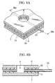
- the second support 6 was laminated by a vacuum laminator on the surface of the second filament group constituted by the plurality of hollow filaments 511 to 518, as shown in FIGS. 6A and 6B .
- a laser beam driller for drilling small diameter holes in a printed circuit board was used for machining of the outer shape, and a hole with ⁇ 0.2 mm was made at an interval of 0.1 mm with a pulse width of 5 ms and four shots, and the support unit was cut into a wide cross shape along the desired cutting line 7 shown in FIG.7B .
- the support unit was cut so as to overlap the portions where the slits 4a, 4b, 4c and 4d had been respectively made in advance in the positions where the eight hollow filaments in 0.4 mm-pitch were collectively in flat cable shape.
- a support unit for a microfluidic system was fabricated so that the support unit had a shape where the first hollow filament group constituted by eight hollow filaments 501 to 508 with an overall length of 20 cm and the second hollow filament group constituted by the hollow filaments 511 to 518 with an overall length of 20 cm were exposed at their ends, and the length of each exposed end was 10 mm. There was no breakage in the entire portions where the hollow filaments were laid, particularly in the portion where the hollow filaments intersect with each other.
- a 0.5 mm-thick aluminum plate was used as the first support 2. Then, as shown in FIG. 2 , a non-stick pressure sensitive adhesive S9009 by Dow Corning Asia Ltd. was laminated onto the surface of the aluminum plate as the first adhesive layer 1a by a roll laminator. Further, as shown in FIGS. 3A and 3B , the release layers 3a, 3b, 3c and 3d made of one-sided release paper were provided as films without stickiness onto the surfaces of the portions of the first adhesive layer 1a, which were near the ends of the hollow filaments and would be unnecessary. The release layers 3a, 3b, 3c were provided so that the release surfaces thereof were closely adhered to the adhesive surface. As shown in FIGS. 4A and 4B and FIGS.
- glass tubes ESG-2 by Hagitec Co. , Ltd. (inner diameter of 0.8 mm and outer diameter of 1 mm) were laid on the above layers by using the NC wiring machine 61 capable of output control of ultrasonic vibration and a load, and capable of moving an X-Y table by NC control.
- a lord of 100g and vibration by an ultrasonic wave with frequency of 20 kHz were applied to the hollow filaments 501 to 508 and 511 to 518 to be laid.
- the hollow filaments 501 to 508 and 511 to 518 were laid to have an arcuate shape with a radius of 10 mm and an intersection therebetween was provided. The load and an ultrasonic vibration were stopped near the intersection.
- Kapton 200H by DuPont Corporation which is the same as the film support, was used as the second support 6 and laminated by a vacuum laminator on the support unit on which the hollow filaments 501 to 508 and 511 to 518 had been laid, as shown in FIGS. 6A and 6B .
- thermocouples for temperature measurement were buried near the inlet, outlet and intersection of the hollow filaments 501 to 508 and 511 to 518.
- the support unit was cut into a desired shape by using an outer shape process machine for a printed circuit board.
- the support unit was cut so as to overlap the portions where the slits 4a, 4b, 4c and 4d had been respectively made in the portion where twelve hollow filaments with 1 mm-pitch were collectively in flat cable shape. Thereafter, the portions of the support, where the non-stick films had been stuck near the ends of the plurality of hollow filaments 501 to 508 and 511 to 518, could be easily removed. Then, a support unit for a microfluidic system was fabricated to have a shape where the twelve hollow filaments 501 to 508 and 511 to 518 with an overall length of 40 cm were exposed with each exposed portion having a length of 50 mm.
- Variations in positions of the flow channels formed by the hollow filaments 501 to 508 and 511 to 518 were within +/-20 ⁇ m or smaller with reference to a design drawing. There was no breakage in the entire portions where the hollow filaments were laid, particularly in the portion where the hollow filaments 501 to 508 and 511 to 518 intersect with each other.
- a film heat FTH-40 by Kyohritsu Electronic Industry Co., Ltd. was stuck to the entire back surface of the aluminum plate and temperature was set at 90 degrees centigrade. Water at about 20 degrees centigrade was flown from the one ends of the hollow filaments, and temperature of water flown out from the other ends was measured. The measured temperature was 88 +/-1 degrees centigrade. Moreover, temperature at the inlet, outlet and intersection was 89 +/- 0.5 degrees centigrade, and temperature could be accurately regulated.
- a copper-clad laminate (plate thickness of 0.2 mm) having 18 ⁇ m-thick copper on its surface was used as the first support 2.
- a pressure sensitive adhesive S9009 by Dow Corning Asia Ltd. (thickness of 200 ⁇ m), which is non-stick at room temperature, was laminated by a roll laminator as the first adhesive layer 1a and the second adhesive layer 1b.
- High-performance engineering plastic tubes by Nirei Industry Co., Ltd.
- the hollow filaments 58 were laid by using a wiring machine for multi-wiring, which is capable of output control of ultrasonic vibration and a load and capable of moving an X-Y table by NC control.
- a load of 80g and vibration by an ultrasonic wave with frequency of 30 kHz were applied to the hollow filaments 58 to be laid.
- the hollow filaments 58 were laid to have an arcuate shape with a radius of 5 mm and an intersection therebetween was provided. The load and ultrasonic vibration was stopped near the intersection.
- the second support 6 was laminated by a vacuum laminator on the surface where the hollow filaments 58 were laid.
- a laser beam driller for small diameter holes in a printed circuit board was used with a pulse width of 5 ms and 4 shots to make a hole with ⁇ 0.2 mm in the second support 6, the first adhesive layer 1a, the second adhesive layer 1b and the hollow filaments 58, at the position which would be the relay portion 8.
- a router was used to process the outer shape, thus fabricating a support unit for a microfluidic system having the relay portion 8 where a plurality of flow channels is connected to each other.
- a through hole is provided in a part of the support unit for a microfluidic system.
- the support unit may be used like a micropump or a microvalve which applies a time-periodic force to a part of a hollow filament 58 by using a motor with a cam, or the like, to deform the hollow filament at the position where the force is applied, thus moving a fluid at the position and causing pulsating flow.
- the hollow filament 58 have elasticity.
- Youngs modulus of the hollow filament 58 is 10 3 MPa or lower.
- the metal film 59 it is possible to form a metal film 59 on a part of the exposed hollow filament 58 to form a terminal to which a voltage or the like is applied.
- the metal film 59 it is preferred that the metal film 59 be formed by plating or deposition of a single layered or multi-layered Cu, Al, nickel (Ni), chrome (Cr), gold (Au), or the like.
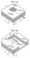
- the support unit for a microfluidic system is provided with the relay portion 8 which is an opening portion.
- the relay portion 8 may have a closed structure without removing the second support 6 as shown in FIG. 10 .
- first hollow filament group and the second hollow filament group do not necessarily intersect with each other at 90 degrees and may only intersect with each other. Therefore, for example, not only the first and second hollow filament groups but also a third hollow filament group may be laid.
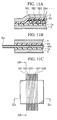
- the hollow filaments do not necessarily intersect with each other. As shown in FIGS. 11A to 11C and 12 , there may be only the first hollow filament group constituted by the plurality of hollow filaments 501 to 508 running in one direction.
- the plurality of hollow filaments 511 to 518 with curvatures may be laid.
- the number of the hollow filaments to be laid is not necessarily plural. In other words, the number of the hollow filaments to be laid may be single.
- a support unit for a microfluidic system which is easily manufactured and has a long flow channel in centimeters that does not limit the number of steps and an amount of a fluid for reaction and analysis.
- a fluidic circuit (a microfluidic system) with good accuracy and fewer manufacturing variations. Further, it is possible to three-dimensionally lay the first hollow filament group constituted by the plurality of hollow filaments and the second hollow filament group constituted by the plurality of hollow filaments, which intersects with the first hollow filament group orthogonally. Thus, a small microfluidic system can be provided even with a complicated flow circuit.
- a support unit for a microfluidic system in which hollow filaments are arrayed to serve as fluidic channels, and a method of manufacturing such a support unit for a microfluidic system with good accuracy and less manufacturing variations.
Abstract

Description
- The present invention relates to a support unit for a microfluidic system, in which a hollow filament is laid on and fixed to a support to have a predetermined shape, and a manufacturing method thereof.
- In chemical and biochemical fields, studies have advanced to miniaturization of reaction systems and analyzers that use microelectromechanical systems (MEMS) . In conventional research and development, there is a micron-scale machine element (referred to as "micromachine" hereinafter) having a single function as a micromotor or micropump.
- In order to conduct an intended chemical reaction or chemical analysis, it is necessary to combine a plurality of various micromachine parts together and systemize them. A complete form of such system is referred to by such names as micro reactor system, or micro total analysis system (µTAS). Usually, micromachines are formed on a silicon chip by applying a semiconductor manufacturing process. In principle, it is possible to form (integrate) a plurality of elements on one chip systemizing them, and efforts have been made in fact toward this operation. However, the fabrication process of the system is complicated, and it is assumed difficult to manufacture the system at a mass production level. A chip substrate (referred to as nanoreactor hereinafter), where a groove is formed as a flow channel by etching or the like at a predetermined position in a silicon substrate, has been suggested as a method of connecting a plurality of micromachines to form a fluidic circuit (system). This method has an advantage in that manufacturing of the system is far easier than manufacturing of the system in the aforementioned method of integration. However, a cross-sectional area of the flow channel is small, and interface resistance between a fluid and the side surface of the groove is large. Thus, under the present circumstances, the maximum length of the flow channel is not more than millimeters, and, in synthetic reactions and chemical reactions that are actually conducted, the number of steps and the amount of a fluid for reaction and analysis are limited.
- However, the fabrication process of the system is complicated, and it is assumed difficult to manufacture the system at a mass production level. Therefore, in recent years, a chip substrate, where a groove is formed as a flow channel by etching or the like at a predetermined position in a silicon substrate, has been suggested as a method of connecting a plurality of micromachines to form a fluidic circuit. This method has an advantage in that manufacturing of the system is far easier than manufacturing of the system in the aforementioned method of integration. However, on the other hand, this method has a problem in that a cross-sectional area of the flow channel is small, and interface resistance between a fluid and the side surface of the groove is large. Thus, under the present circumstances, the maximum length of the flow channel is not more than millimeters, and, in synthetic reactions and chemical reactions that are actually conducted, the number of steps and the amount of a fluid for reaction and analysis are limited.
- The present invention was accomplished to resolve the above-described problem. In other words, an object of the present invention is to provide a support unit for a microfluidic system, which is manufactured easily and has a long flow channel in centimeters that does not limit the number of steps and an amount of a fluid for reaction and analysis.
- Another object of the present invention is to provide a support unit for a small microfluidic system, which does not require space even with a complicated fluidic circuit.
- Yet another object of the present invention is to provide a manufacturing method for a support unit for a microfluidic system, in which a complicated fluidic circuit can be formed.
- In order to achieve the above object, a first aspect of the present invention inheres in a support unit for a microfluidic system including (a) a first support, (b) a first adhesive layer provided on a surface of the first support, (c) a hollow filament laid on a surface of the first adhesive layer to have an arbitrary shape, and (d) a hollow filament laid on the surface of the first adhesive layer to have an arbitrary shape and functioning as a flow channel layer of a microfluidic system. In the first aspect of the present invention, another hollow filament can be three-dimensionally laid in a manner of intersecting with said hollow filament. Therefore, it becomes possible to provide a support unit for a microfluidic system which has good accuracy, can be manufactured easily and has a long flow channel in centimeters that does not limit the number of steps and the amount of a fluid for reaction and analysis. Further, according to the first aspect of the present invention, it is possible to provide a support unit for a small microfluidic system, which does not require space even with a complicated fluidic circuit. Thus, it is also possible to downsize the microfluidic system itself.
- A second aspect of the present invention inheres in a support unit for a microfluidic system including (a) a first support, (b) a first adhesive layer provided on a surface of the first support, and (c) a first hollow filament group constituted by a plurality of hollow filaments laid on a surface of the first adhesive layer to have an arbitral shape and respectively functioning as a plurality of flow channel layers of the microfluidic system. In the second aspect of the present invention, a second hollow filament group constituted by a plurality of hollow filaments can be three-dimensionally laid to intersect the first hollow filament group constituted by the plurality of hollow filaments. Therefore, it becomes possible to provide a support unit for a microfluidic system which has good accuracy, can be manufactured easily and has a long flow channel in centimeters that does not limit the number of steps and the amount of a fluid for reaction and analysis. Further, according to the first aspect of the present invention, it is possible to provide a support unit for a small microfluidic system, which does not require space even with a complicated fluidic circuit. Thus, it is also possible to downsize the microfluidic system itself.
- A third aspect of the present invention inheres in a manufacturing method of a support unit for a microfluidic system including (a) forming a first adhesive layer on a surface of a first support, and (b) laying a hollow filament on a surface of the first adhesive layer. The manufacturing method of a support unit for a microfluidic system according to the third aspect of the present invention is a manufacturing method using the support unit for a microfluidic system explained in the first aspect. According to the third aspect of the present invention, it is possible to provide a manufacturing method of a support unit for a small microfluidic system in which a complicated fluidic circuit can be formed.
- A fourth aspect of the present invention inheres in a manufacturing method of a support unit for a microfluidic system including (a) forming a first adhesive layer on a surface of a first support, and (b) laying a first hollow filament group constituted by a plurality of hollow filaments on a surface of the first adhesive layer. The manufacturing method of a support unit for a microfluidic system according to the fourth aspect of the present invention is a manufacturing method using the support unit for a microfluidic system described in the second aspect. According to the fourth aspect of the present invention, it is possible to provide a manufacturing method of a support unit for a small microfluidic system in which a complicated fluidic circuit can be formed.
-
-
Fig.1 is a cross sectional view of a support unit for a microfluidic system according to a first embodiment of the present invention, andFIG. 1B is a plan view whose cross section along the line IA-IA viewed in the arrow direction corresponds toFIG. 1A . -
FIG. 2 is a process cross sectional view (No.1) explaining a manufacturing method of the support unit for a microfluidic system according to the first embodiment of the present invention. -
FIG. 3A is a process cross sectional view (No. 2) explaining the manufacturing method of the support unit for a microfluidic system according to the first embodiment of the present invention, andFIG. 3B is a plan view whose cross section along the line IIIA-IIIA viewed in the arrow direction corresponds toFIG. 3A . -
FIG. 4A is a process cross sectional view (No. 3) explaining the manufacturing method of the support unit for a microfluidic system according to the first embodiment of the present invention, andFIG. 4B is a plan view whose cross section along the line IVA-IVA viewed in the arrow direction corresponds toFIG. 4A . -
FIG. 5A is a process cross sectional view (No. 4) explaining the manufacturing method of the support unit for a microfluidic system according to the first embodiment of the present invention, andFIG. 5B is a plan view whose cross section along the line VA-VA viewed in the arrow direction corresponds toFIG. 5A . -
FIG. 6A is a process cross sectional view (No. 5) explaining the manufacturing method of the support unit for a microfluidic system according to the first embodiment of the present invention, andFIG. 6B is a plan view whose cross section along the line VIA-VIA viewed in the arrow direction corresponds toFIG. 6A . -
FIG, 7A is a process cross sectional view (No. 6) explaining the manufacturing method of the support unit for a microfluidic system according to the first embodiment of the present invention, andFIG. 7B is a plan view whose cross section along the line VIIA-VIIA viewed in the arrow direction corresponds toFIG. 7A . -
FIG. 8A is a bird's eye view of a support unit for a microfluidic system including a relay portion according to a second embodiment of the present invention, andFIG. 8B is a cross sectional view along the line VIIIB- VIIIB. -
FIG. 9A is a bird's eye view (No. 1) explaining a configuration of a hollow filament for a support unit for a microfluidic system according to another embodiment of the present invention, andFIG. 9B is a bird's eye view (No. 2) explaining a configuration of a hollow filament for a support unit for a microfluidic system according to another embodiment of the present invention. -
FIG. 10 is a cross sectional view of a support unit for a microfluidic system including a relay portion according to another embodiment of the present invention. -
FIG. 11A is a cross sectional view viewed in the arrow direction along the line XIA-XIA of a plan view of a support unit for a microfluidic system shown inFIG. 11C , according to yet another embodiment of the present invention,FIG. 11B is a cross sectional view viewed in the arrow direction along the line XIB-XIB of the plan view shown inFIG. 11C . -
FIG. 12 is a bird's eye view of the support unit for a microfluidic system according to yet another embodiment of the present invention shown inFIGS. 11A to 11C . -
FIG. 13 is a bird's eye view showing a modification of the support unit for a microfluidic system according to yet another embodiment of the present invention. - Embodiments of the present invention are described with reference to the drawings. The same or similar parts are denoted by the same or similar symbols. However, the drawings are schematic, and a relation between a thickness and a dimension of a plane, a ratio between thicknesses of respective layers, and the like are different from those in reality. Therefore, specific thicknesses and dimensions should be determined by checking the description below. In addition, between the drawings, relationship and ratio between dimensions may of course be different.
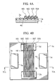
- As shown in
FIGS. 1A and 1B , a support unit for a microfluidic system according to a first embodiment of the present invention includes afirst support 2, a first adhesive layer 1a provided on a surface of thefirst support 2, a first hollow filament group constituted by a plurality ofhollow filaments hollow filaments adhesive layer 1b provided on a surface of the second hollow filament group, and asecond support 6 provided on a surface of the secondadhesive layer 1b. The first hollow filament group constituted by the plurality ofhollow filaments hollow filaments - The inner diameters and outer diameters of the plurality of
hollow filaments 501 to 508 and 511 to 518 may be selected depending on a purpose. However, the inner diameters preferably range from about φ 0.05 mm to φ 0.5 mm since milliliters (mL) to microliters (µL) of fluid is flown therethrough. In fabricating thehollow filaments 501 to 508 and 511 to 518 with the above diameters, particularly suitable materials for the hollow filaments are polyimide (PI), polyether ether ketone (PEEK), polyether imide (PEI), polyphenylene sulfide (PPS), tetrafluoroethylene-perfluoroalkoxyethylene copolymer (PFA), and the like. With inner diameters of φ 0.05 mm or smaller, an influence of the interface resistance between the fluid and the inner wall surfaces of thehollow filaments 501 to 508 and 511 to 518 becomes too great to be ignored. On the other hand, with inner diameters larger than φ 0.5 mm, high pressure is required to allow the fluid to flow continuously, thus causing an increase in burdens on other parts and mixing of air bubbles into the fluid. When causing a chemical reaction in the fluid flowing through the first hollow filament group constituted by the plurality ofhollow filaments 501 to 508 and the second hollow filament group constituted by the plurality ofhollow filaments 511 to 518 , it is preferred that thehollow filaments 501 to 508 and 511 to 518 be chemical resistant. Further, when causing a photochemical reaction or performing spectroscopic analysis by illuminating the fluid flowing through thehollow filaments 501 to 508 and 511 to 518, it is preferred that thehollow filaments 501 to 508 and 511 to 518 be transparent. A value of light transmittance may depend on purpose, but the value is preferably 80% or more with a target wavelength, and the value of 90% or more is optimal. In other words, as shown inFIG. 9A , it is preferred that thesecond support 6, the secondadhesive layer 1b, and ahollow filament 58 be transparent at a predetermined position, or that thehollow filament 58 be exposed and at least the exposed portion of thehollow filament 58 be transparent. - In comparison with a free state, fixing the
hollow filaments 501 to 508 and 511 to 518 to thefirst support 2 produces an excellent advantage in that various environments around the hollow filaments such as temperature, an electric field, and a magnetic field can be easily controlled. This is advantageous in performing a chemical reaction or chemical analysis, and is particularly essential for micronized reaction system and analysis system. There is another advantage in that thehollow filaments 501 to 508 and 511 to 518 are easily aligned with and connected to parts, and a number of thehollow filaments 501 to 508 and 511 to 518 can be accommodated compactly. - Further, when performing chemical analysis, providing the plurality of
hollow filaments 501 to 508 and 511 to 518 is advantageous in that operation efficiency is improved. In this case, it is required that the lengths of the plurality ofhollow filaments 501 to 508 constituting the first hollow filament group are equal to each other from a viewpoint that, when the analysis starts simultaneously in the hollow filaments, results of the analysis should be obtained almost simultaneously. Similarly, it is required that the lengths of the plurality ofhollow filaments 511 to 518 constituting the second hollow filament group are equal to each other. In other words, it is important that amounts of energy applied from the outside to the inlets through the outlets for a sample are uniform, and that there is little difference between the amounts of energy applied to the hollow filaments. From this viewpoint, it is preferred that thehollow filaments 501 to 508 and 511 to 518 be sandwiched by at least two supports so that distribution of heat conducted through thehollow filaments 501 to 508 and 511 to 518 is uniform. - Moreover, it is preferred that the plurality of
hollow filaments 501 to 508 constituting the first hollow filament group and the plurality ofhollow filaments 511 to 518 constituting the second hollow filament group be arrayed at mutually equal intervals. Furthermore, it is preferred that the plurality ofhollow filaments 501 to 508 constituting the first hollow filament group and the plurality ofhollow filaments 511 to 518 constituting the second hollow filament group have a uniform tube thickness. - Commercially available tubes made from various materials can be used for the plurality of
hollow filaments 501 to 508 and 511 to 518, and tubes made of an arbitrary material may be selected depending on a purpose. These materials include, for example, an organic material such as polyvinyl chloride resin (PVC), polyvinylidene chloride resin, polyvinyl acetate resin, polyvinyl alcohol resin (PVA), polystyrene resin (PS), acrylonitrile butadiene styrene copolymer (ABS), polyethylene resin (PE), ethylene-vinyl acetate copolymer (EVA), polypropylene resin (PP), poly-4-methylpentene (TPX), polymethyl methacrylate (PMMA), PEEK, PI, PEI, PPS, cellulose acetate, polytetrafluoroethylene resin (PTFE), tetrafluoroethylene-hexafluoropropylene resin (FEP), PFA, polyethylene-tetrafluoroethylene copolymer (ETFE), polychlorotrifluoro-ethylene (PCTFE), polyvinylidene fluoride (PVDF), polyethylene terephthalate resin (PET), polyamide resin (nylon), polyacetal (POM), polyphenylene terephthalate (PPT), polycarbonate resin (PC), polyurethane resin, polyesterelastomer, polyolefin resin, silicone resin, and polyimide resin, and an inorganic material such as glass, quartz, and carbon. - Material type, shape and size of the
first support 2 may be selected depending on a purpose. An appropriate range of the board thickness or film thickness of thefirst support 2 is differentiated depending on a purpose or a required function. For example, where electrical insulation properties are required in thefirst support 2, selected is an epoxy resin board or a polyimide resin board used for a printed wiring board, a polyimide film represented by Kapton film by DuPont Corporation used for a flexible printed wiring board, or a PET film represented by Lumirror Film by Toray Industries Inc. It is preferred that thefirst support 2 have a large board thickness (film thickness), and the thickness of 0.05 mm or larger is particularly preferred. Moreover, where heat dissipation properties are required in thefirst support 2, a metal board such as an aluminum (Al) board, a copper (Cu) board, a stainless steel board, and a titanium (Ti) board is selected. It is preferred that the thickness of thefirst support 2 is even thicker, and the thickness of 0.5 mm or larger is particularly preferred. Further, where light transmittivity is required in thefirst support 2, selected is a board made of a transparent inorganic material such as glass and quartz, or a board or film made of a transparent organic material such as polycarbonate and acryl. It is preferred that thefirst support 2 has a small board thickness (film thickness), and a thickness of 0.5 mm or smaller is particularly preferred. It is also possible to use so-termed flexible circuit board or printed circuit board in which a metal pattern such as a copper pattern is formed on the surface of thefirst support 2 by etching or plating. In virtue of this, it becomes possible to form a terminal or a circuit which implements various parts and elements such as a micromachine, a heater element, a piezoelectric element, various sensors including those of temperature, pressure, distortion, vibration, voltage, magnetic field, and the like, an electronic part such as a resistor, a capacitor, a coil, a transistor, and an IC, and an optical part such as a laser diode (LD), a light emitting diode (LED) and a photodiode (PD) . Thus, systemization becomes easy. - The first adhesive layer 1a formed on the surface of the
first support 2 is preferably a pressure sensitive or photosensitive adhesive. These materials realize stickiness or adhesion by application of pressure or light thereto. Therefore, these materials are suitable for the case where the hollow filaments (hollow capillaries) are mechanically laid. As for the pressure sensitive adhesive, a high-molecular weight synthetic rubber adhesive or a silicone resin adhesive is appropriate. The high-molecular weight synthetic rubber may be, for example, polyisobutylene such as Vistanex MML-120 by Tonex Co., Ltd., acrylonitrile-butadiene rubber such as Nipol N1432 by Zeon Corporation, chlorosulfonated polyethylene such as Hypalon 20 by DuPont Corporation, and the like. In this case, the first adhesive layer 1a can be formed in a manner that these materials are dissolved into a solvent, applied directly onto thefirst support 2 and dried. Further, a crosslinking agent may be compounded in these materials as necessary. It is also possible to use a pressure sensitive adhesive double coated tape made of acrylic resin, such as No. 500 by Nitto Denko Corporation, A-10, A-20, A-30 or the like by 3M Corporation, and the like. As for the silicone resin adhesive, a suitable adhesive is a silicone rubber made from high-molecular weight polydimethylsiloxane or polymethylphenylsiloxane and containing terminal silanol groups, or a silicone adhesive whose main ingredient is a silicone resin like a methyl silicone resin or a methylphenyl silicone resin. Various crosslinking can be performed in order to control cohesive strength. For example, crosslinking can be performed by an addition reaction of silane, a condensation reaction of alkoxy, a condensation reaction of acetoxy, and a radical reaction by peroxide or the like. Commercially available adhesives of the above kind include YR3286 (product name, produced by GE Toshiba Silicones Co. , Ltd.), TSR1521 (product name, produced by GE Toshiba Silicones Co., Ltd.), DKQ9-9009 (product name, produced by Dow Corning Corporation) and the like. As for the photosensitive adhesive, for example, a dry film resist used as an etching resist of a printed circuit board, a solder resist ink, a photosensitive buildup material of a printed circuit board can be employed. Specifically, H-K440 by Hitachi Chemical Co., Ltd., Probimer by Ciba-Geigy Corporation or the like can be used. Particularly, a photovia material provided for use in a buildup wiring board is durable to a manufacturing process of a printed wiring board and to a process of mounting parts by soldering. Any kind of material can be used as such material as long as it is a copolymer containing functional groups which can be crosslinked by light, or a composition containing monomer, and/or a composition obtained by mixing functional groups which can be crosslinked by heat in stead of light and a thermal polymerization initiator. - The first adhesive layer 1a may be epoxy resin, brominated epoxy resin, cycloaliphatic epoxy resin such as rubber-modified epoxy resin and rubber-dispersed epoxy resin, or bisphenol A epoxy resin and acid modifications of these epoxy resins. Particularly, when photo-curing is performed by illumination, modifications made of these epoxy resins and unsaturated acid are preferred. Unsaturated acid may include maleic anhydride, tetrahydrophthalic anhydride, itaconic acid anhydride, acrylic acid, methacrylic acid, and the like. These modifications are obtained by reacting unsaturated carboxylic acid with epoxy groups of epoxy resin with a compounding ratio in which an amount of unsaturated carboxylic acid is equal to or less than epoxy groups. Apart from the above, a thermosetting material such as melamine resin and cyanate ester resin, or a combination of such thermosetting material and phenolic resin is also a part of favorable application examples. In addition, a combination of such resin and a material which adds flexibility is also favorable. Examples of this include acrylonitrile-butadiene rubber, natural rubber, acrylic rubber, SBR, carboxylic acid-modified acrylonitrile-butadiene rubber, carboxylic acid-modified acrylic rubber, crosslinking NBR particles, carboxylic acid-modified crosslinking NBR particles and the like. By adding various resin components, a curing material can be provided with various properties while maintaining basic properties such as photo-curing and thermosetting. For example, a combination with epoxy resin or phenolic resin can add good electrical insulating properties to a curing material. When a rubber component is compounded, a curing material is provided with toughness, and, at the same time, the surface of the curing material can be roughened easily by surface treatment using an oxidizing chemical solution. Further, additives (polymerization stabilizer, leveling agent, pigment, dye and the like), which are commonly used, may also be added. It is perfectly acceptable to compound a filler. The filler may include inorganic microparticles such as silica, fused silica, talc, alumina, hydrated alumina, barium sulfate, calcium hydroxide, aerosol, and calcium carbonate, organic microparticles such as powdered epoxy resin and powdered polyimide particles, and powdered polytetrafluoroethylene particles. These fillers may be subjected to coupling treatment in advance. Dispersion of these fillers can be achieved by a known mixing method such as a kneader, a ball mill, a bead mill, and a triple-roll mill. A method of forming a photosensitive resin of this kind may be a coating method such as a roll coating, curtain coating and dip coating, and a method of producing films of an insulating resin on a carrier film and sticking the films together by a laminator. Specifically, a photo-via film BF-8000 by Hitachi Chemical Co., Ltd. or the like can be used.
- Earlier-described various materials for the
first support 2 can be used for thesecond support 6. Further, the secondadhesive layer 1b is inserted between thesecond support 6 and the second hollow filament group constituted by the plurality ofhollow filaments 511 to 518. This is preferable since the first hollow filament group constituted by the plurality ofhollow filaments 501 to 508 and the second hollow filament group constituted by the plurality ofhollow filaments 511 to 518 are provided with increased protection. By selecting a mesh-like film or a porous film as thesecond support 6, a problem such as trapped air bubbles when laminating becomes difficult. This mesh-like film or a fabric may be a polyester mesh TB-70 by Tokyo Screen Co., Ltd. The porous film may be Duragard by Celanese Chemicals, Ltd. , Celgard 2400 by Daicel Chemical Industries, Ltd., for example. - The earlier-described various materials for the first adhesive layer 1a can be used for the second
adhesive layer 1b. - Next, a manufacturing method of the support unit for a microfluidic system according to the first embodiment of the present invention is described using
FIGS. 2 to 8 . - (a) First of all, as shown in
FIG. 2 , the first adhesive layer 1a is formed on the surface of thefirst support 2 to have the same shape and approximately the same size as thefirst support 2. Then, as shown inFIGS. 3A and 3B , four rectangle release layers 3a, 3b, 3c, and 3d are equally formed on the peripheral portions of the surface of the first adhesive layer 1a. These release layers 3a, 3b, 3c and 3d are formed on the surface of the first adhesive layer 1a by a method of applying a commercially available release agent or sticking release-films to predetermined portions of the surface of the first adhesive layer 1a. Next, slits 4a, 4b, 4c and 4d are provided in thefirst support 2 by a cutter or the like. For example, the slits are made at positions adjacent to the inner lines of the respective fourrelease layers - (b) Next, as shown in
FIGS. 4A and 4B , the first hollow filament group constituted by the plurality ofhollow filaments 501 to 508 is laid in a vertical direction from therelease layer 3b towards therelease layer 3d, on the surface of thefirst support 2 on which the first adhesive layer 1a is formed. Although not illustrated, anNC wiring machine 61 similar to that shown inFIG. 5A is used when laying the first hollow filament group. (There is a wiring machine disclosed inJapanese Patent Laid-Open Publication (Kokai) No. 2001-59910 Japanese Examined. Patent Publication (Kokoku) No. Showa 50 (1975) -9346 Japanese Examined Patent Publication (Kokoku) No. Heisei 7 (1995)-95622 NC wiring machine 61 is numerically controlled and is capable of controlling outputs of ultrasonic vibration and a load. By using thisNC wiring machine 61, a laid pattern of the first hollow filament group constituted by the plurality ofhollow filaments 501 to 508 can be precisely controlled. Specifically, theNC wiring machine 61 applies a load and vibration by an ultrasonic wave to the first hollow filament group constituted by thehollow filaments 501 to 508, while moving in parallel with thefirst support 2. - (c) Next, as shown in
FIGS. 5A and 5B , the second hollow filament group constituted by the plurality ofhollow filaments 511 to 518 is laid in a direction from therelease layer 3a towards therelease layer 3c intersecting with the first hollow filament group constituted by the plurality ofhollow filaments 501 to 508 which has already been laid. As shown inFIG. 5A , theNC wiring machine 61 is used when laying the second hollow filament group. Thus, a laid pattern of the second hollow filament group constituted by the plurality ofhollow filaments 511 to 518 can be controlled precisely. Specifically, theNC wiring machine 61 applies a load and vibration by an ultrasonic wave to the second hollow filament group constituted by the plurality ofhollow filaments 511 to 518, while moving in parallel with thefirst support 2. However, theNC wiring machine 61 is set to stop a load and ultrasonic vibration at the position where the first hollow filament group constituted by thehollow filaments 501 to 508 and the second hollow filament group constituted by thehollow filaments 511 to 518 intersect with each other. By stopping a load and/or ultrasonic vibration near the intersection of the first hollow filament group and the second hollow filament group, stress on thehollow filaments 501 to 508 and 511 to 518 is reduced, and breakage of thehollow filaments 501 to 508 and 511 to 518 can be prevented. - (d) Next, as shown in
FIGS. 6A and 6B , the secondadhesive layer 1b having the same shape and almost the same size as thefirst support 2 is formed so as to cover the first hollow filament group constituted by the plurality ofhollow filaments 501 to 508 and the second hollow filament group constituted by the plurality ofhollow filaments 511 to 518, which have already been laid. Further, thesecond support 6 having the same shape and size as thefirst support 2 is prepared and adhered (laminated) onto the secondadhesive layer 1b. Various methods are considered for laminating thesecond support 6. Where thesecond support 6 is a mesh-like film or a porous film, this protection film can be closely adhered to the secondadhesive layer 1b without air trapped in the interface, by applying a little pressure. However, where thesecond support 6 is a uniform film, there is no way to avoid air bubbles remaining in the interface. In this case, pressing the film with high pressure may be considered, but a large force is applied onto thehollow filaments 501 to 508 and 511 to 518 and the hollow portions of the filaments are deformed. Further, there is a problem in that, for example, a large force is locally applied onto the intersection between the first hollow filament group and the second hollow filament group, and the filaments at the intersection are broken. In such a case, it is preferred to use a vacuum laminating machine to create a vacuum state before thesecond support 6 is closely adhered to the secondadhesive layer 1b and, thereafter, to press and bond thesecond support 6 to the secondadhesive layer 1b at low pressure. This is because there will be no air trapped in the interface, and a large stress does not remain in thehollow filaments 501 to 508 and 511 to 518, causing no breakage of the hollow filaments. - (e) Thereafter, the support unit is cut along a
cutting line 7 in a desired shape shown by a dotted line inFIG. 7B . A method of making the support unit for a microfluidic system into the desired shape is cutting the support unit by a cutter or cutting the same by pressing a metal blade fabricated to have the desired shape in advance. However, automation of cutting with a cutter is difficult, and, as for the blade, fabrication of jigs takes time and effort. Therefore, it is preferred to use an NC driven laser beam machine as it only requires data preparation to operate. Further, with regard to the laser beam machine, it is preferred to use a laser beam driller for drilling small diameter holes in a printed circuit board rather than a machine with a large output designated for cutting. The laser beam driller for a printed circuit board is preferred since it has a large energy output per unit period, drills a hole by a plurality of shots at the same position, and moves by a measure of about half the diameter of the hole, thus causing the very small number of laser scorches. As shown inFIG. 7B , the support unit is cut along acutting line 7 set so as to overlappositions 4a where theslits FIG. 7A , by making theslits adhesive layer 1b are automatically peeled off near the end of thehollow filament 518. Although not illustrated, at the ends of the otherhollow filaments 501 to 508, 511, 512, 513, ···, 517, the first adhesive layer 1a and the secondadhesive layer 1b are similarly peeled off automatically. The first hollow filament group constituted by the plurality ofhollow filaments 501 to 508 and the second hollow filament group constituted by the plurality ofhollow filaments 511 to 518 are laid on the first adhesive layer 1a. Thereafter, thesecond support 6 is adhered to the hollow filaments through the secondadhesive layer 1b. With this construction, a process of exposing the ends of the plurality ofhollow filaments 501 to 508 and 511 to 518 becomes complicated. Therefore, theslits first support 2, thus facilitating the process of exposing the ends of thehollow filaments 501 to 518 and 511 to 518. - (f) After cutting the support unit along the
cutting line 7 shown by the dotted line inFIG. 7B , therelease layer 3b and therelease layer 3d positioned near the ends of thehollow filaments 501 to 508 are removed, and further, therelease layer 3a and therelease layer 3c positioned near the ends of thehollow filaments 511 to 518 are removed. Thus, the support unit for a microfluidic system shown inFIGS. 1A and 1B is completed. - As described above, the release layers 3a, 3b, 3c and 3d are provided on the surfaces of the ends of the
first support 2 which become unnecessary and are ultimately removed, as shown inFIGS. 4A and 4B . This makes it even easier to carry out the process of drawing out the first hollow filament group constituted by the plurality ofhollow filaments 501 to 508 and the second hollow filament group constituted by the plurality ofhollow filaments 511 to 518 respectively from the ends of the support unit for a microfluidic system. However, care should be taken for the lengths of the exposed portions of thehollow filaments 501 to 508 and 511 to 518. The reason is as follows. The unexposed portions of thehollow filaments 501 to 508 and 511 to 518 are fixed, and it is thus easy to control factors such as temperature, flow velocity distribution, electrophoretic velocity distribution, and applied voltage, of the fluid within thehollow filaments 501 to 508 and 511 to 518. Meanwhile, the exposed portions of thehollow filaments 501 to 508 and 511 to 518 are not fixed and are in a free state, and it is thus difficult to control each of the above factors. Further, careless handling easily causes breakage of the exposed portions of thehollow filaments 501 to 508 and 511 to 518. Therefore, it is important to make the lengths of the exposed portions as short as possible, and it is preferred that the lengths of the exposed portions be at least shorter than the lengths of the unexposed portions. - Moreover, in the manufacturing method of the support unit for a microfluidic system according to the first embodiment of the present invention, the hollow members (hollow filaments) 501 to 508 and 511 to 518 are used. Therefore, appropriate thoughts should be put into design and manufacturing. Apart from the laying conditions on the intersection between the first hollow filament group and the second hollow filament group, there are thoughts put on forming conditions of the
second support 6 serving as a protection film layer. Further, considerations should be made regarding laying conditions of the respective straight portions of the first hollow filament group constituted by the plurality ofhollow filaments 501 to 508 and the second hollow filament group constituted by the plurality ofhollow filaments 511 to 518 , and curvature conditions on thehollow filaments 501 to 508 and 511 to 518. These conditions cannot be set generally since they largely depend on the material of thehollow filaments 501 to 508 and 511 to 518 and the specification of the first adhesive layer 1a. In other words, it is required to set design and manufacturing conditions suitable for thehollow filaments 501 to 508 and 511 to 518 and the first adhesive layer 1a to be used. If this operation is neglected, good hollow portions cannot be ensured and, in addition, defects occur in thehollow filaments 501 to 508 and 511 to 518, causing incidents such as leakage of a fluid. - As shown in
FIGS. 8A and 8b , a support unit for a microfluidic system according to a second embodiment of the present invention is different from the support unit for a microfluidic system according to the first embodiment of the present invention shown inFIGS. 1A and 1B in that the support unit for a microfluidic system according to the second embodiment has anrelay portion 8. The first adhesive layer 1a, the secondadhesive layer 1b, and thesecond support 6 form the wall portion of therelay portion 8, and thefirst support 2 is the bottom portion of the same. The rest is similar to the first embodiment, and duplicated description is thus omitted. - As shown in
FIGS. 8A and 8B , therelay portion 8 has a construction wherehollow filaments 58 are exposed between the first adhesive layer 1a and the secondadhesive layer 1b. The exposedhollow filaments 58 discharge a fluid. Therelay portion 8 enables the discharged fluid to be mixed or branched. The shape and size of therelay portion 8 may be decided depending on the flow quantity of the fluid. For example, where the total thickness of flow channels formed by two or threehollow filaments 58 with φ 200 µm, and the first adhesive layer 1a and the secondadhesive layer 1b, which hold thehollow filaments 58, is 200 µm, therelay portion 8 may have a cylindrical shape with about φ 2 mm to φ 7 mm. - Laser beam machining is preferred for removal of the first adhesive layer 1a, the second
adhesive layer 1b, and thehollow filaments 58 at a predetermined position which becomes therelay portion 8. Laser beam machining is particularly preferred where the volume of the removed portion, that is, the volume of therelay portion 8 is as small as a volume in cubic millimeters or smaller. A laser used for laser beam machining is a carbon dioxide gas laser, a YAG laser, an excimer laser, and the like, and may be selected depending on the materials of the first adhesive layer 1a, the secondadhesive layer 1b, and thehollow filament 58. Note that, where therelay portion 8 is formed by a laser, it is preferred to use thefirst support 2 with a metal thin film such as a copper or aluminum film formed on the surface thereof. The metal thin film serves as a laser beam stopper. When the volume of therelay portion 8 is in cubic centimeters or larger and a large area is thus removed, machining by a drill or the like may be applied. In the case of machining, a desmear treatment for removing resin shavings produced while cutting is added. - A method of allowing the
second support 6 to be a part of therelay portion 8 may be a process of machining thesecond support 6 to have a shape so that thesecond support 6 becomes a part of therelay portion 8. This process is carried out after thesecond support 6 is adhered to the secondadhesive layer 1b. In this case, a method of sticking thesecond support 6 by a needle such as an injection needle, or the like, is appropriate. - Further, another method may be a method of machining the
second support 6 to have a shape so that thesecond support 6 becomes a part ofrelay portion 8, simultaneously with the formation of therelay portion 8 in the first adhesive layer 1a and the secondadhesive layer 1b. In this case, a method of machining the entire layers at once by the foregoing laser, or the like, is appropriate. - Further, yet another method may be a method of machining the
second support 6 in advance to have a shape so that thesecond support 6 becomes a part of therelay portion 8, and then adhering thesecond support 6 to the secondadhesive layer 1b. The method of machining thesecond support 6 may be drilling, punching, laser beam machining or the like. - According to the support unit for a microfluidic system according to the second embodiment of the present invention, provision of the
relay potion 8 makes it possible to mix or branch a fluid flowing through thehollow filaments 58. Further, thesecond support 6 becomes a part of therelay portion 8. Thus, therelay portion 8 can have an open structure, enabling a new fluid to be filled into the relay portion from outside and enabling the fluid within therelay portion 8 to be removed. - Kapton 300H by DuPont Corporation with a thickness of 75 µm was used as the
first support 2. On the surface of thefirst support 2, a VBH A-10 film by 3M Corporation having a thickness of 250 µm and stickiness at room temperature was laminated by a roll laminator as shown inFIG. 2 . As shown inFIGS. 3A and 3B , one-sided release paper was provided as the release layers 3a, 3b, 3c and 3d at desired positions on thefirst support 2 so that the release surfaces were closely adhered to the adhesive surface. Further, as shown inFIGS. 4A and 4B , theslits first support 2. Then, as shown inFIG. 5A , thehollow filaments 501 to 508 and 511 to 518 constituted by high-performance engineering plastic tubes by Nirei Industry Co. , Ltd. (material: PEEK, inner diameter of 0.2 mm, outer diameter 0.4 mm) 62 were laid onto thefirst support 2 by using anNC wiring machine 61 which is capable of output control of ultrasonic vibration and a load and capable of moving an X-Y table by NC control. A lord of 80g and vibration by an ultrasonic wave with frequency of 30 kHz were applied to thehollow filaments 501 to 508 and 511 to 518 to be laid. As shown inFIG. 5B , thehollow filaments 501 to 508 and 511 to 518 were laid to have an arcuate shape with a radius of 5mm and an intersection therebetween was provided. The load and ultrasonic vibration could be stopped near the intersection. Kapton 300H by DuPont Corporation, on which a VBH A-10 film by 3M Corporation was laminated by the use of a roll laminator, was used as thesecond support 6. Thesecond support 6 was laminated by a vacuum laminator on the surface of the second filament group constituted by the plurality ofhollow filaments 511 to 518, as shown inFIGS. 6A and 6B . Thereafter, a laser beam driller for drilling small diameter holes in a printed circuit board was used for machining of the outer shape, and a hole with φ 0.2 mm was made at an interval of 0.1 mm with a pulse width of 5 ms and four shots, and the support unit was cut into a wide cross shape along the desiredcutting line 7 shown inFIG.7B . At this time, the support unit was cut so as to overlap the portions where theslits first support 2, where the release layers 3a, 3b, 3c and 3d had been stuck near the ends of thehollow filaments 501 to 508 and 511 to 518, could be easily removed. Then, a support unit for a microfluidic system was fabricated so that the support unit had a shape where the first hollow filament group constituted by eighthollow filaments 501 to 508 with an overall length of 20 cm and the second hollow filament group constituted by thehollow filaments 511 to 518 with an overall length of 20 cm were exposed at their ends, and the length of each exposed end was 10 mm. There was no breakage in the entire portions where the hollow filaments were laid, particularly in the portion where the hollow filaments intersect with each other. - As a result, variations in positions of the flow channels formed by the first hollow filament group constituted by the plurality of
hollow filaments 501 to 508 and the second hollow filament group constituted by the plurality ofhollow filaments 511 to 518 were within +/-10 µm or smaller with reference to a design drawing. The support unit for a microfluidic system was put in a thermoregulator, and the temperature was maintained at 80 degrees centigrade. Liquid color ink was then flown from one ends of the hollow filaments, and duration of time until the ink was flown out were measured by a measurement instrument such as a stopwatch. The ink flew out from the other ends of the eight hollow filaments almost at the same moment (+/- 1 second or shorter). - A 0.5 mm-thick aluminum plate was used as the
first support 2. Then, as shown inFIG. 2 , a non-stick pressure sensitive adhesive S9009 by Dow Corning Asia Ltd. was laminated onto the surface of the aluminum plate as the first adhesive layer 1a by a roll laminator. Further, as shown inFIGS. 3A and 3B , the release layers 3a, 3b, 3c and 3d made of one-sided release paper were provided as films without stickiness onto the surfaces of the portions of the first adhesive layer 1a, which were near the ends of the hollow filaments and would be unnecessary. The release layers 3a, 3b, 3c were provided so that the release surfaces thereof were closely adhered to the adhesive surface. As shown inFIGS. 4A and 4B andFIGS. 5A and 5B , glass tubes ESG-2 by Hagitec Co. , Ltd. (inner diameter of 0.8 mm and outer diameter of 1 mm) were laid on the above layers by using theNC wiring machine 61 capable of output control of ultrasonic vibration and a load, and capable of moving an X-Y table by NC control. A lord of 100g and vibration by an ultrasonic wave with frequency of 20 kHz were applied to thehollow filaments 501 to 508 and 511 to 518 to be laid. As shown inFIG. 5B , thehollow filaments 501 to 508 and 511 to 518 were laid to have an arcuate shape with a radius of 10 mm and an intersection therebetween was provided. The load and an ultrasonic vibration were stopped near the intersection. Kapton 200H by DuPont Corporation, which is the same as the film support, was used as thesecond support 6 and laminated by a vacuum laminator on the support unit on which thehollow filaments 501 to 508 and 511 to 518 had been laid, as shown inFIGS. 6A and 6B . At this time, thermocouples for temperature measurement were buried near the inlet, outlet and intersection of thehollow filaments 501 to 508 and 511 to 518. Thereafter, for machining of the outer shape shown inFIGS. 7A and 7B , the support unit was cut into a desired shape by using an outer shape process machine for a printed circuit board. At this time, the support unit was cut so as to overlap the portions where theslits hollow filaments 501 to 508 and 511 to 518, could be easily removed. Then, a support unit for a microfluidic system was fabricated to have a shape where the twelvehollow filaments 501 to 508 and 511 to 518 with an overall length of 40 cm were exposed with each exposed portion having a length of 50 mm. Variations in positions of the flow channels formed by thehollow filaments 501 to 508 and 511 to 518 were within +/-20 µm or smaller with reference to a design drawing. There was no breakage in the entire portions where the hollow filaments were laid, particularly in the portion where thehollow filaments 501 to 508 and 511 to 518 intersect with each other. - A film heat FTH-40 by Kyohritsu Electronic Industry Co., Ltd. was stuck to the entire back surface of the aluminum plate and temperature was set at 90 degrees centigrade. Water at about 20 degrees centigrade was flown from the one ends of the hollow filaments, and temperature of water flown out from the other ends was measured. The measured temperature was 88 +/-1 degrees centigrade. Moreover, temperature at the inlet, outlet and intersection was 89 +/- 0.5 degrees centigrade, and temperature could be accurately regulated.
- As shown in
FIGS. 8A and 8B , a copper-clad laminate (plate thickness of 0.2 mm) having 18 µm-thick copper on its surface was used as thefirst support 2. On the surface of the copper-clad laminate, a pressure sensitive adhesive S9009 by Dow Corning Asia Ltd. (thickness of 200 µm), which is non-stick at room temperature, was laminated by a roll laminator as the first adhesive layer 1a and the secondadhesive layer 1b. High-performance engineering plastic tubes by Nirei Industry Co., Ltd. (material: PEEK, inner diameter of 0.2 mm, outer diameter of 0.4 mm) were laid by using a wiring machine for multi-wiring, which is capable of output control of ultrasonic vibration and a load and capable of moving an X-Y table by NC control. A load of 80g and vibration by an ultrasonic wave with frequency of 30 kHz were applied to thehollow filaments 58 to be laid. Thehollow filaments 58 were laid to have an arcuate shape with a radius of 5 mm and an intersection therebetween was provided. The load and ultrasonic vibration was stopped near the intersection. Kapton 200H by DuPont Corporation, on which S9009 by Dow Corning Asia Ltd. (thickness of 200 µm) was laminated by a roll laminator, was used as thesecond support 6. Thesecond support 6 was laminated by a vacuum laminator on the surface where thehollow filaments 58 were laid. - Thereafter, a laser beam driller for small diameter holes in a printed circuit board was used with a pulse width of 5 ms and 4 shots to make a hole with φ 0.2 mm in the
second support 6, the first adhesive layer 1a, the secondadhesive layer 1b and thehollow filaments 58, at the position which would be therelay portion 8. Thereafter, a router was used to process the outer shape, thus fabricating a support unit for a microfluidic system having therelay portion 8 where a plurality of flow channels is connected to each other. - The present invention has been described based on the foregoing aspects. However, it should be understood that the sections and drawings constituting a part of this disclosure do not limit this invention. Various alternative embodiments, examples and application technologies will be apparent to those skilled in the art from this disclosure.
- For example, as shown in
FIG. 9A , a through hole is provided in a part of the support unit for a microfluidic system. The support unit may be used like a micropump or a microvalve which applies a time-periodic force to a part of ahollow filament 58 by using a motor with a cam, or the like, to deform the hollow filament at the position where the force is applied, thus moving a fluid at the position and causing pulsating flow. In this case, it is preferred that thehollow filament 58 have elasticity. In particular it is preferred that Youngs modulus of thehollow filament 58 is 103 MPa or lower. - Moreover, as shown in
FIG. 9B , it is possible to form ametal film 59 on a part of the exposedhollow filament 58 to form a terminal to which a voltage or the like is applied. In this case, it is preferred that themetal film 59 be formed by plating or deposition of a single layered or multi-layered Cu, Al, nickel (Ni), chrome (Cr), gold (Au), or the like. - Further, as shown in
FIGS. 8A and 8B , the support unit for a microfluidic system is provided with therelay portion 8 which is an opening portion. However, where therelay portion 8 is only for mixing or branching a fluid, therelay portion 8 may have a closed structure without removing thesecond support 6 as shown inFIG. 10 . - Furthermore, the first hollow filament group and the second hollow filament group do not necessarily intersect with each other at 90 degrees and may only intersect with each other. Therefore, for example, not only the first and second hollow filament groups but also a third hollow filament group may be laid.
- On the other hand, the hollow filaments do not necessarily intersect with each other. As shown in
FIGS. 11A to 11C and12 , there may be only the first hollow filament group constituted by the plurality ofhollow filaments 501 to 508 running in one direction. - Moreover, as shown in
FIG. 13 , the plurality ofhollow filaments 511 to 518 with curvatures may be laid. - Note that the number of the hollow filaments to be laid is not necessarily plural. In other words, the number of the hollow filaments to be laid may be single.
- As described above, according to the present invention, it is possible to provide a support unit for a microfluidic system, which is easily manufactured and has a long flow channel in centimeters that does not limit the number of steps and an amount of a fluid for reaction and analysis.
- As a result, according to the present invention, it is possible to provide a fluidic circuit (a microfluidic system) with good accuracy and fewer manufacturing variations. Further, it is possible to three-dimensionally lay the first hollow filament group constituted by the plurality of hollow filaments and the second hollow filament group constituted by the plurality of hollow filaments, which intersects with the first hollow filament group orthogonally. Thus, a small microfluidic system can be provided even with a complicated flow circuit.
- Moreover, according to the present invention, it is possible to provide a support unit for a microfluidic system in which hollow filaments are arrayed to serve as fluidic channels, and a method of manufacturing such a support unit for a microfluidic system with good accuracy and less manufacturing variations.
- Further embodiments are listed below:
- 1. A support unit for a microfluidic system, comprising:
- a first support;
- a first adhesive layer provided on a surface of the first support; and
- a hollow filament laid on a surface of the first adhesive layer to have an arbitrary shape and functioning as a flow channel layer of the microfluidic system.
- 2. A support unit for a microfluidic system, comprising:
- a first support;
- a first adhesive layer provided on a surface of the first support; and
- a first hollow filament group constituted by a plurality of hollow filaments laid on a surface of the first adhesive layer and respectively functioning as a plurality of flow channel layers of the microfluidic system.
- 3. The support unit for a microfluidic system according to 2, further comprising:
- a second adhesive layer provided on a surface of the first hollow filament group; and
- a second support provided on a surface of the second adhesive layer.
- 4. The support unit for a microfluidic system according to 2 or 3, further comprising a second hollow filament group constituted by a plurality of hollow filaments laid in a direction so as to intersect with the first hollow filament group and functioning as another plurality of flow channel layers of the microfluidic system.
- 5. The support unit for a microfluidic system according to any one of 2 to 4, wherein the plurality of hollow filaments is partially exposed from the first support.
- 6. The support unit for a microfluidic system according to any one of 2 to 5, wherein a metal film is formed on a part of at least one of the plurality of hollow filaments.
- 7. The support unit for a microfluidic system according to any one of 2 to 6, wherein at least one of the plurality of hollow filaments is partially provided with an optically transparent portion.
- 8. A support unit for a microfluidic system, comprising:
- a first support;
- a first adhesive layer provided on a surface of the first support;
- a plurality of hollow filaments laid on a surface of the first adhesive layer;
- a second adhesive layer provided on the first adhesive layer and the hollow filaments;
- a second support provided on a surface of the second adhesive layer; and
- a relay portion provided in the first adhesive layer and the second adhesive layer and connecting routes of the hollow filaments.
- 9. The support unit for a microfluidic system according to 8, wherein the relay portion includes a part of the second support.
- 10. A manufacturing method of a support unit for a microfluidic system, comprising:
- forming a first adhesive layer on a surface of a first support; and
- laying a hollow filament on a surface of the first adhesive layer.
- 11. A manufacturing method of a support unit for a microfluidic system, comprising:
- forming a first adhesive layer on a surface of a first support; and
- laying a first hollow filament group constituted by a plurality of hollow filaments, on a surface of the first adhesive layer.
- 12. The manufacturing method of a support unit for a microfluidic system according to 11, between the forming the first adhesive layer and laying the first hollow filament group, the manufacturing method further comprising:
- providing release layers on the surface of the first adhesive layer at positions where the hollow filaments are exposed; and
- providing a slit in the first support,
- wherein the first hollow filament group is laid to be in contact with both surfaces of a pair of the release layers.
- 13. The manufacturing method of a support unit for a microfluidic system according to 11 or 12, further comprising the laying a second hollow filament group constituted by a plurality of hollow filaments in a direction so as to intersect with the first hollow filament group, after the laying the first hollow filament group.
- 14. The manufacturing method of a support unit for a microfluidic system according to 11 or 12, after the laying the first hollow filament group, the manufacturing method further comprising:
- forming a second adhesive layer on a surface of the first hollow filament group; and
- adhering a second support onto a surface of the second adhesive layer.
- 15. A manufacturing method of a support unit for a microfluidic system, comprising:
- forming a first adhesive layer on a surface of a first support;
- laying a plurality of hollow filaments on a surface of the first adhesive layer;
- forming a second adhesive layer on the first adhesive layer and the hollow filaments;
- forming a relay portion in the first adhesive layer and the second adhesive layer; and
- adhering a second support onto a surface of the second adhesive layer.
- 16. The manufacturing method of a support unit for a microfluidic system according to 15, wherein the forming the relay portion in the first adhesive layer and the second adhesive layer further includes forming the relay portion so that the second support becomes a part of the relay portion.
Claims (11)
- A support unit for a microfluidic system, comprising:a first support;a first adhesive layer provided on a surface of the first support; andat least two equal hollow filaments disposed on a surface of the first adhesive layer in an arbitrary shape and functioning as a flow channel layer of the microfluidic system.
- The support unit for a mircorfluidic system according to claim 1, wherein of the hollow filaments of equal length form a group and more than two groups are provided.
- The support unit for a microfluidic system according to claim 1 or 2, wherein the hollow filament is partially exposed from the first support.
- The support unit for a microfluidic system according to claim 1 or 3, wherein an end of the hollow filament exposes from the first support.
- The support unit for a microfluidic system according to claim 1 or 4, wherein a metal film is formed on a part of at least one hollow filament.
- The support unit for a microfluidic system according to any one of claims 1 to 5, wherein at least one hollow filament is partially provided with an optically transparent portion.
- The support unit for a microfluidic system according to any one of claims 1 to 6, wherein at least one hollow filament has light permeability.
- The support unit for a microfluidic system according to any one of claims 1 to 7, wherein the laying shape of the hollow filament is fixed by the first adhesive layer.
- The support unit for a microfluidic system according to any one of claims 1 to 8, wherein there is a cavity in the circumference of the hollow filament.
- The support unit for a microfluidic system according to any one of claims 1 to 9, wherein a terminal or a circuit is formed on the surface of at least one of the first support and the second support.
- The support unit for a microfluidic system according to any one of claims 1 to 10, wherein at least one part which is chosen among a micromachine, a generation of heat element, a piezoelectric element, a sensor, an electronic part, a light part is formed on the surface of at least one of the first support and the second support.
Applications Claiming Priority (4)
| Application Number | Priority Date | Filing Date | Title |
|---|---|---|---|
| JP2002048580 | 2002-02-25 | ||
| JP2002292978 | 2002-10-04 | ||
| JP2003046414A JP3933058B2 (en) | 2002-02-25 | 2003-02-24 | Support unit for microfluidic system and method for manufacturing the same |
| EP03707062A EP1486455B1 (en) | 2002-02-25 | 2003-02-25 | Support unit for microfluidic system and manufacturing method |
Related Parent Applications (2)
| Application Number | Title | Priority Date | Filing Date |
|---|---|---|---|
| EP03707062.0 Division | 2003-02-25 | ||
| EP03707062A Division EP1486455B1 (en) | 2002-02-25 | 2003-02-25 | Support unit for microfluidic system and manufacturing method |
Publications (3)
| Publication Number | Publication Date |
|---|---|
| EP1902781A2 true EP1902781A2 (en) | 2008-03-26 |
| EP1902781A3 EP1902781A3 (en) | 2008-04-02 |
| EP1902781B1 EP1902781B1 (en) | 2011-06-29 |
Family
ID=27761226
Family Applications (8)
| Application Number | Title | Priority Date | Filing Date |
|---|---|---|---|
| EP10177308.3A Withdrawn EP2255870A3 (en) | 2002-02-25 | 2003-02-25 | A manufacturing method of a support unit for a microfluidic system |
| EP08000282A Expired - Lifetime EP1913998B1 (en) | 2002-02-25 | 2003-02-25 | A support unit for a microfluidic system |
| EP08000284A Expired - Lifetime EP1902781B1 (en) | 2002-02-25 | 2003-02-25 | A support unit for a microfluidic system |
| EP03707062A Expired - Lifetime EP1486455B1 (en) | 2002-02-25 | 2003-02-25 | Support unit for microfluidic system and manufacturing method |
| EP08000283A Withdrawn EP1902780A3 (en) | 2002-02-25 | 2003-02-25 | A support unit for a microfluidic system |
| EP08000280A Expired - Lifetime EP1902779B1 (en) | 2002-02-25 | 2003-02-25 | A support unit for a microfluidic system |
| EP08000281A Expired - Lifetime EP1913997B1 (en) | 2002-02-25 | 2003-02-25 | A support unit for a microfluidic system |
| EP08000285A Withdrawn EP1902782A3 (en) | 2002-02-25 | 2003-02-25 | A support unit for a microfluidic system |
Family Applications Before (2)
| Application Number | Title | Priority Date | Filing Date |
|---|---|---|---|
| EP10177308.3A Withdrawn EP2255870A3 (en) | 2002-02-25 | 2003-02-25 | A manufacturing method of a support unit for a microfluidic system |
| EP08000282A Expired - Lifetime EP1913998B1 (en) | 2002-02-25 | 2003-02-25 | A support unit for a microfluidic system |
Family Applications After (5)
| Application Number | Title | Priority Date | Filing Date |
|---|---|---|---|
| EP03707062A Expired - Lifetime EP1486455B1 (en) | 2002-02-25 | 2003-02-25 | Support unit for microfluidic system and manufacturing method |
| EP08000283A Withdrawn EP1902780A3 (en) | 2002-02-25 | 2003-02-25 | A support unit for a microfluidic system |
| EP08000280A Expired - Lifetime EP1902779B1 (en) | 2002-02-25 | 2003-02-25 | A support unit for a microfluidic system |
| EP08000281A Expired - Lifetime EP1913997B1 (en) | 2002-02-25 | 2003-02-25 | A support unit for a microfluidic system |
| EP08000285A Withdrawn EP1902782A3 (en) | 2002-02-25 | 2003-02-25 | A support unit for a microfluidic system |
Country Status (10)
| Country | Link |
|---|---|
| US (9) | US20050249637A1 (en) |
| EP (8) | EP2255870A3 (en) |
| JP (1) | JP3933058B2 (en) |
| KR (8) | KR100984452B1 (en) |
| CN (5) | CN101096009A (en) |
| AT (5) | ATE514478T1 (en) |
| AU (1) | AU2003211695A1 (en) |
| DE (1) | DE60326323D1 (en) |
| TW (1) | TW579367B (en) |
| WO (1) | WO2003070623A1 (en) |
Families Citing this family (38)
| Publication number | Priority date | Publication date | Assignee | Title |
|---|---|---|---|---|
| JP3933058B2 (en) * | 2002-02-25 | 2007-06-20 | 日立化成工業株式会社 | Support unit for microfluidic system and method for manufacturing the same |
| US20050100712A1 (en) * | 2003-11-12 | 2005-05-12 | Simmons Blake A. | Polymerization welding and application to microfluidics |
| ATE448018T1 (en) * | 2004-02-18 | 2009-11-15 | Hitachi Chemical Co Ltd | MICROFLUIDIC UNIT WITH HOLLOW FIBER CHANNEL |
| EP1838723A4 (en) * | 2004-06-29 | 2008-10-08 | Univ Cincinnati | Polymorphisms and haplotypes of the alpha 2c adrenergic receptor gene |
| US8097225B2 (en) * | 2004-07-28 | 2012-01-17 | Honeywell International Inc. | Microfluidic cartridge with reservoirs for increased shelf life of installed reagents |
| WO2006059649A1 (en) | 2004-11-30 | 2006-06-08 | Hitachi Chemical Co., Ltd. | Component for preanalytical treatment |
| CN102172507A (en) * | 2004-12-09 | 2011-09-07 | 日立化成工业株式会社 | Support unit for micro fluid system and process for producing the same |
| US7390377B1 (en) * | 2005-09-22 | 2008-06-24 | Sandia Corporation | Bonding thermoplastic polymers |
| US8011768B2 (en) * | 2006-08-23 | 2011-09-06 | Canon Kabushiki Kaisha | Ink tank |
| JP2008281366A (en) * | 2007-05-08 | 2008-11-20 | Hitachi Chem Co Ltd | Support unit for microfluid system |
| JP5012186B2 (en) * | 2007-05-08 | 2012-08-29 | 日立化成工業株式会社 | Method for manufacturing support unit for microfluidic system |
| JP5217323B2 (en) * | 2007-09-14 | 2013-06-19 | 株式会社明電舎 | Bipolar multilayer electric double layer capacitor |
| JP5262064B2 (en) * | 2007-10-30 | 2013-08-14 | 富士ゼロックス株式会社 | Reaction method using microreactor and microreactor |
| US20090149256A1 (en) * | 2007-12-07 | 2009-06-11 | Kam Lim Lui | Joystick for Video Game Machine |
| CN201133614Y (en) * | 2007-12-07 | 2008-10-15 | 付强 | TV video game machine light emitting rod |
| WO2009139407A1 (en) * | 2008-05-16 | 2009-11-19 | 日本化薬株式会社 | Microanalysis chip adhesive sheet, microanalysis chip, and manufacturing method thereof |
| US8354080B2 (en) | 2009-04-10 | 2013-01-15 | Canon U.S. Life Sciences, Inc. | Fluid interface cartridge for a microfluidic chip |
| EP2871482B1 (en) * | 2012-07-09 | 2018-07-18 | Sony Corporation | Microchip and method for producing microchip |
| KR101475906B1 (en) * | 2014-04-30 | 2014-12-23 | 박동현 | A preprocessing kit for detecting pesticide residues based on micro-fluidics chip and the detection method using the same |
| US10585518B2 (en) * | 2014-10-15 | 2020-03-10 | Microsoft Technology Licensing, Llc | Display module support |
| EP3085661B1 (en) * | 2015-04-21 | 2017-12-27 | JSR Corporation | Method of producing microfluidic device |
| US10388849B2 (en) | 2016-01-29 | 2019-08-20 | Microjet Technology Co., Ltd. | Piezoelectric actuator |
| US10615329B2 (en) | 2016-01-29 | 2020-04-07 | Microjet Technology Co., Ltd. | Piezoelectric actuator |
| US9976673B2 (en) | 2016-01-29 | 2018-05-22 | Microjet Technology Co., Ltd. | Miniature fluid control device |
| US10371136B2 (en) | 2016-01-29 | 2019-08-06 | Microjet Technology Co., Ltd. | Miniature pneumatic device |
| EP3203080B1 (en) | 2016-01-29 | 2021-09-22 | Microjet Technology Co., Ltd | Miniature pneumatic device |
| US10388850B2 (en) | 2016-01-29 | 2019-08-20 | Microjet Technology Co., Ltd. | Piezoelectric actuator |
| EP3203081B1 (en) | 2016-01-29 | 2021-06-16 | Microjet Technology Co., Ltd | Miniature fluid control device |
| US10584695B2 (en) | 2016-01-29 | 2020-03-10 | Microjet Technology Co., Ltd. | Miniature fluid control device |
| US10451051B2 (en) | 2016-01-29 | 2019-10-22 | Microjet Technology Co., Ltd. | Miniature pneumatic device |
| US10487821B2 (en) | 2016-01-29 | 2019-11-26 | Microjet Technology Co., Ltd. | Miniature fluid control device |
| US10487820B2 (en) | 2016-01-29 | 2019-11-26 | Microjet Technology Co., Ltd. | Miniature pneumatic device |
| US10529911B2 (en) | 2016-01-29 | 2020-01-07 | Microjet Technology Co., Ltd. | Piezoelectric actuator |
| US10639744B2 (en) * | 2016-05-05 | 2020-05-05 | The Hong Kong Polytechnic University | Method of laser joining of dissimilar materials with ultrasonic aid |
| US10683861B2 (en) | 2016-11-10 | 2020-06-16 | Microjet Technology Co., Ltd. | Miniature pneumatic device |
| US10746169B2 (en) | 2016-11-10 | 2020-08-18 | Microjet Technology Co., Ltd. | Miniature pneumatic device |
| TWI690657B (en) * | 2016-11-10 | 2020-04-11 | 研能科技股份有限公司 | Micro-fluid control device |
| US10655620B2 (en) | 2016-11-10 | 2020-05-19 | Microjet Technology Co., Ltd. | Miniature fluid control device |
Citations (3)
| Publication number | Priority date | Publication date | Assignee | Title |
|---|---|---|---|---|
| JPS509346B1 (en) | 1969-10-09 | 1975-04-11 | ||
| JPH0795622B2 (en) | 1985-07-19 | 1995-10-11 | アドバンスト インターコネクション テクノロジー インコーポレイテッド | Equipment for manufacturing or modifying conductor laying circuit boards |
| JP2001059910A (en) | 1999-06-17 | 2001-03-06 | Graphtec Corp | Device for wiring optical fiber and method for wiring optical fiber |
Family Cites Families (80)
| Publication number | Priority date | Publication date | Assignee | Title |
|---|---|---|---|---|
| US3702658A (en) | 1971-02-24 | 1972-11-14 | Du Pont | Permeation separation apparatus |
| US3852716A (en) | 1973-03-02 | 1974-12-03 | Staid Inc | Point-of-sale processing system |
| US3915652A (en) | 1973-08-16 | 1975-10-28 | Samuel Natelson | Means for transferring a liquid in a capillary open at both ends to an analyzing system |
| JPS62280367A (en) | 1986-05-30 | 1987-12-05 | Hitachi Electronics Eng Co Ltd | Cooling type vapor phase reactor |
| US5070606A (en) * | 1988-07-25 | 1991-12-10 | Minnesota Mining And Manufacturing Company | Method for producing a sheet member containing at least one enclosed channel |
| US4970034A (en) | 1988-09-23 | 1990-11-13 | W. R. Grace & Co.-Conn. | Process for preparing isotropic microporous polysulfone membranes |
| US5236665A (en) | 1988-10-20 | 1993-08-17 | Baxter International Inc. | Hollow fiber treatment apparatus and membrane oxygenator |
| US4959152A (en) * | 1989-03-24 | 1990-09-25 | The Standard Oil Company | Hollow fiber separation module and method for the use thereof |
| US5174900A (en) | 1989-03-24 | 1992-12-29 | The Standard Oil Company | Apparatus for separation and for treatment of fluid feedstreams, wafers for use therein and related methods |
| JP3003714B2 (en) | 1991-03-29 | 2000-01-31 | 日本電信電話株式会社 | Mobile communication termination control method |
| EP0521495A3 (en) * | 1991-07-05 | 1993-03-10 | Akzo N.V. | Process and apparatus for manufacturing hollow fibre modules |
| US5264171A (en) | 1991-12-31 | 1993-11-23 | Hoechst Celanese Corporation | Method of making spiral-wound hollow fiber membrane fabric cartridges and modules having flow-directing baffles |
| JPH0682190A (en) | 1992-09-01 | 1994-03-22 | Kobe Steel Ltd | Aluminum cooling plate for forced liquid cooling |
| DE4308697A1 (en) * | 1993-03-18 | 1994-09-22 | Durst Franz Prof Dr Dr H C | Process for enriching a first gaseous or liquid medium with a second gas or a second liquid and a reactor for carrying out the process |
| US5534328A (en) | 1993-12-02 | 1996-07-09 | E. I. Du Pont De Nemours And Company | Integrated chemical processing apparatus and processes for the preparation thereof |
| KR100327521B1 (en) | 1993-03-19 | 2002-07-03 | 이.아이,듀우판드네모아앤드캄파니 | Integrated chemical processing device and its manufacturing method |
| US5429807A (en) * | 1993-10-28 | 1995-07-04 | Beckman Instruments, Inc. | Method and apparatus for creating biopolymer arrays on a solid support surface |
| EP1157743B1 (en) | 1993-10-28 | 2009-03-11 | Houston Advanced Research Center | Microfabricated, flowthrough porous apparatus for discrete detection of binding reactions |
| GB9405518D0 (en) * | 1994-03-21 | 1994-05-04 | Mupor Ltd | Porous metal composite body |
| US5591139A (en) * | 1994-06-06 | 1997-01-07 | The Regents Of The University Of California | IC-processed microneedles |
| GB9414444D0 (en) | 1994-07-18 | 1994-09-07 | Secr Defence | Cvd diamond coating of elongate substrate material |
| US5540464A (en) * | 1994-10-04 | 1996-07-30 | J&W Scientific Incorporated | Capillary connector |
| EP0725272B1 (en) | 1995-02-01 | 2002-06-12 | Metrohm Ag | Device for ion chromatography and process for cyclic regeneration of several suppressors in such a device |
| US5716825A (en) | 1995-11-01 | 1998-02-10 | Hewlett Packard Company | Integrated nucleic acid analysis system for MALDI-TOF MS |
| EP0830899B1 (en) * | 1996-01-10 | 2003-08-20 | Asahi Kasei Kabushiki Kaisha | Paint recovering method and collecting material |
| US5799817A (en) * | 1996-02-16 | 1998-09-01 | Sharp; Bruce R. | Storage tank systems with encapsulated flow paths |
| US5628425A (en) | 1996-05-10 | 1997-05-13 | Sharp; Bruce R. | Composite storage tank having double wall characteristics |
| NZ333346A (en) | 1996-06-28 | 2000-03-27 | Caliper Techn Corp | High-throughput screening assay systems in microscale fluidic devices |
| US5779897A (en) | 1996-11-08 | 1998-07-14 | Permea, Inc. | Hollow fiber membrane device with inert filaments randomly distributed in the inter-fiber voids |
| GB9625491D0 (en) | 1996-12-07 | 1997-01-22 | Central Research Lab Ltd | Fluid connections |
| US5789143A (en) * | 1997-04-30 | 1998-08-04 | Eastman Kodak Company | Thioethers in photographic elements |
| US5955353A (en) * | 1997-05-22 | 1999-09-21 | Excorp Medical, Inc. | Hollow fiber bioreactor with an extrafilament flow plug |
| JP3469585B2 (en) | 1997-05-23 | 2003-11-25 | ガメラ バイオサイエンス コーポレイション | Apparatus and method for using centripetal acceleration to drive flow motion in microfluidics systems |
| WO1999006589A1 (en) | 1997-08-01 | 1999-02-11 | Minnesota Mining And Manufacturing Company | Method and devices for detecting and enumerating microorganisms |
| JPH11156184A (en) | 1997-11-27 | 1999-06-15 | Toyo Eng Corp | Specimen synthesis device |
| JPH11211694A (en) | 1998-01-29 | 1999-08-06 | Yuichi Mori | Capillary and its manufacture |
| NL1008315C2 (en) | 1998-02-16 | 1999-08-25 | Stichting Fund Ond Material | Microdialysis probe integrated with Si chip. |
| DE59911948D1 (en) | 1998-03-01 | 2005-05-25 | Klaus Rennebeck | METHOD AND DEVICE FOR OBTAINING SYNTHESEGAS |
| JP2000015065A (en) | 1998-07-03 | 2000-01-18 | Hitachi Ltd | Hollow fiber membrane carrying catalyst |
| JP2000019145A (en) * | 1998-07-06 | 2000-01-21 | Nippon Telegr & Teleph Corp <Ntt> | Electrochemical detector and its manufacture |
| US6387234B1 (en) | 1998-08-31 | 2002-05-14 | Iowa State University Research Foundation, Inc. | Integrated multiplexed capillary electrophoresis system |
| JP3419691B2 (en) | 1998-09-04 | 2003-06-23 | 日本電信電話株式会社 | Ultra-small flow cell and method for producing the same |
| AU6151599A (en) * | 1998-09-18 | 2000-04-10 | University Of Utah Research Foundation | Surface micromachined microneedles |
| US7048723B1 (en) * | 1998-09-18 | 2006-05-23 | The University Of Utah Research Foundation | Surface micromachined microneedles |
| US6592559B1 (en) | 1998-12-09 | 2003-07-15 | Cook Incorporated | Hollow, curved, superlastic medical needle |
| CZ9900769A3 (en) * | 1999-03-04 | 2000-10-11 | Petr Ing. Drsc. Hušek | Use of tip with filter for making sorbent column of defined volume within the space underneath the filter |
| JP2000246092A (en) | 1999-03-04 | 2000-09-12 | Kawamura Inst Of Chem Res | Production of microchemical device |
| EP1595948A3 (en) | 1999-03-05 | 2006-03-01 | Mitsubishi Rayon Co., Ltd. | Carriers having biological substance |
| JP2001248072A (en) | 2000-03-02 | 2001-09-14 | Mitsubishi Rayon Co Ltd | Method for treating inner wall part of hollow fiber and method for packing gel |
| US6148508A (en) * | 1999-03-12 | 2000-11-21 | Caliper Technologies Corp. | Method of making a capillary for electrokinetic transport of materials |
| DE19912541C1 (en) * | 1999-03-19 | 2000-10-26 | Karlsruhe Forschzent | Process for killing harmful microorganisms in liquids by briefly heating them up |
| US6436292B1 (en) | 1999-04-02 | 2002-08-20 | Symyx Technologies, Inc. | Parallel high-performance liquid chromatography with post-separation treatment |
| US6256533B1 (en) | 1999-06-09 | 2001-07-03 | The Procter & Gamble Company | Apparatus and method for using an intracutaneous microneedle array |
| US20020015952A1 (en) * | 1999-07-30 | 2002-02-07 | Anderson Norman G. | Microarrays and their manufacture by slicing |
| US6713309B1 (en) * | 1999-07-30 | 2004-03-30 | Large Scale Proteomics Corporation | Microarrays and their manufacture |
| US6423536B1 (en) * | 1999-08-02 | 2002-07-23 | Molecular Dynamics, Inc. | Low volume chemical and biochemical reaction system |
| DE60035199T2 (en) * | 1999-08-11 | 2008-02-14 | Asahi Kasei Kabushiki Kaisha | ANALYSIS CASSETTE AND LIQUID CONVEYOR CONTROLLER |
| JP3506652B2 (en) | 2000-03-22 | 2004-03-15 | 株式会社日立製作所 | Capillary array electrophoresis device |
| WO2001077683A1 (en) | 2000-04-06 | 2001-10-18 | Caliper Technologies Corp. | Methods and devices for achieving long incubation times in high-throughput systems |
| US6632400B1 (en) * | 2000-06-22 | 2003-10-14 | Agilent Technologies, Inc. | Integrated microfluidic and electronic components |
| US6893733B2 (en) | 2000-07-07 | 2005-05-17 | Delphi Technologies, Inc. | Modified contoured crushable structural members and methods for making the same |
| FR2813073A1 (en) * | 2000-12-19 | 2002-02-22 | Commissariat Energie Atomique | Device for biological, chemical, pharmaceutical and medical uses, comprises channels and a reception area for guiding and positioning capillaries to connect to a micro-fluidic component |
| JP4385541B2 (en) | 2001-04-02 | 2009-12-16 | 三菱化学株式会社 | Flow-through microreaction channel, reaction apparatus and reaction method |
| US6719147B2 (en) | 2001-04-27 | 2004-04-13 | The University Of Delaware | Supported mesoporous carbon ultrafiltration membrane and process for making the same |
| US6837988B2 (en) | 2001-06-12 | 2005-01-04 | Lifescan, Inc. | Biological fluid sampling and analyte measurement devices and methods |
| WO2003022330A2 (en) | 2001-09-12 | 2003-03-20 | Becton, Dickinson And Company | Microneedle-based pen device for drug delivery and method for using same |
| US20030070752A1 (en) | 2001-09-27 | 2003-04-17 | Kevin Bergevin | Method of manufacture for fluid handling barrier ribbon with polymeric tubes |
| JP3686999B2 (en) | 2001-11-01 | 2005-08-24 | 株式会社産学連携機構九州 | Method for producing functional membrane and functional membrane |
| US7004928B2 (en) | 2002-02-08 | 2006-02-28 | Rosedale Medical, Inc. | Autonomous, ambulatory analyte monitor or drug delivery device |
| JP3933058B2 (en) | 2002-02-25 | 2007-06-20 | 日立化成工業株式会社 | Support unit for microfluidic system and method for manufacturing the same |
| JP4221505B2 (en) | 2002-07-18 | 2009-02-12 | 独立行政法人産業技術総合研究所 | Manufacturing method of microreactor and microreactor |
| JP3805292B2 (en) * | 2002-08-26 | 2006-08-02 | 日立化成工業株式会社 | Electrophoresis member, method for producing the same, and capillary electrophoresis apparatus |
| TW536524B (en) | 2002-09-17 | 2003-06-11 | Fan-Gen Tzeng | Network-type micro-channel device for micro-fluid |
| DE10345817A1 (en) | 2003-09-30 | 2005-05-25 | Boehringer Ingelheim Microparts Gmbh | Method and apparatus for coupling hollow fibers to a microfluidic network |
| ATE448018T1 (en) * | 2004-02-18 | 2009-11-15 | Hitachi Chemical Co Ltd | MICROFLUIDIC UNIT WITH HOLLOW FIBER CHANNEL |
| US7818077B2 (en) | 2004-05-06 | 2010-10-19 | Valve Corporation | Encoding spatial data in a multi-channel sound file for an object in a virtual environment |
| JP2005326068A (en) | 2004-05-13 | 2005-11-24 | Daikin Ind Ltd | Plate for heat exchanger and heat exchanger |
| WO2006059649A1 (en) * | 2004-11-30 | 2006-06-08 | Hitachi Chemical Co., Ltd. | Component for preanalytical treatment |
| CN102172507A (en) | 2004-12-09 | 2011-09-07 | 日立化成工业株式会社 | Support unit for micro fluid system and process for producing the same |
| WO2007087421A2 (en) * | 2006-01-23 | 2007-08-02 | Avantis Medical Systems, Inc. | Endoscope |
-
2003
- 2003-02-24 JP JP2003046414A patent/JP3933058B2/en not_active Expired - Lifetime
- 2003-02-25 AT AT08000280T patent/ATE514478T1/en not_active IP Right Cessation
- 2003-02-25 EP EP10177308.3A patent/EP2255870A3/en not_active Withdrawn
- 2003-02-25 CN CNA2006101427349A patent/CN101096009A/en active Pending
- 2003-02-25 KR KR1020047013114A patent/KR100984452B1/en active IP Right Grant
- 2003-02-25 AT AT08000281T patent/ATE514480T1/en not_active IP Right Cessation
- 2003-02-25 KR KR1020077030260A patent/KR20080009764A/en not_active Application Discontinuation
- 2003-02-25 KR KR1020067016792A patent/KR100984956B1/en not_active IP Right Cessation
- 2003-02-25 KR KR1020077030259A patent/KR100984403B1/en not_active IP Right Cessation
- 2003-02-25 EP EP08000282A patent/EP1913998B1/en not_active Expired - Lifetime
- 2003-02-25 EP EP08000284A patent/EP1902781B1/en not_active Expired - Lifetime
- 2003-02-25 KR KR1020097025349A patent/KR101009209B1/en not_active IP Right Cessation
- 2003-02-25 CN CN2006101427334A patent/CN101096008B/en not_active Expired - Fee Related
- 2003-02-25 CN CN038045672A patent/CN1639054B/en not_active Expired - Fee Related
- 2003-02-25 EP EP03707062A patent/EP1486455B1/en not_active Expired - Lifetime
- 2003-02-25 EP EP08000283A patent/EP1902780A3/en not_active Withdrawn
- 2003-02-25 CN CN2010105743695A patent/CN102086015A/en active Pending
- 2003-02-25 KR KR1020067016790A patent/KR100984919B1/en not_active IP Right Cessation
- 2003-02-25 CN CN200610142732XA patent/CN101096007B/en not_active Expired - Fee Related
- 2003-02-25 AT AT08000284T patent/ATE514479T1/en not_active IP Right Cessation
- 2003-02-25 KR KR1020077030261A patent/KR100984431B1/en not_active IP Right Cessation
- 2003-02-25 EP EP08000280A patent/EP1902779B1/en not_active Expired - Lifetime
- 2003-02-25 AT AT03707062T patent/ATE423618T1/en not_active IP Right Cessation
- 2003-02-25 WO PCT/JP2003/002066 patent/WO2003070623A1/en active Application Filing
- 2003-02-25 KR KR1020067016791A patent/KR100984938B1/en active IP Right Grant
- 2003-02-25 AT AT08000282T patent/ATE514481T1/en not_active IP Right Cessation
- 2003-02-25 EP EP08000281A patent/EP1913997B1/en not_active Expired - Lifetime
- 2003-02-25 US US10/505,416 patent/US20050249637A1/en not_active Abandoned
- 2003-02-25 AU AU2003211695A patent/AU2003211695A1/en not_active Abandoned
- 2003-02-25 EP EP08000285A patent/EP1902782A3/en not_active Withdrawn
- 2003-02-25 DE DE60326323T patent/DE60326323D1/en not_active Expired - Lifetime
- 2003-02-25 TW TW092103929A patent/TW579367B/en not_active IP Right Cessation
-
2009
- 2009-07-01 US US12/496,212 patent/US8889084B2/en not_active Expired - Fee Related
- 2009-07-10 US US12/501,056 patent/US20090274581A1/en not_active Abandoned
- 2009-07-10 US US12/501,108 patent/US20090274584A1/en not_active Abandoned
- 2009-07-10 US US12/501,078 patent/US8865090B2/en not_active Expired - Fee Related
- 2009-07-10 US US12/501,120 patent/US20090274585A1/en not_active Abandoned
- 2009-07-10 US US12/501,097 patent/US20090274583A1/en not_active Abandoned
- 2009-07-14 US US12/502,394 patent/US20090274586A1/en not_active Abandoned
-
2010
- 2010-10-28 US US12/914,010 patent/US20110036479A1/en not_active Abandoned
Patent Citations (3)
| Publication number | Priority date | Publication date | Assignee | Title |
|---|---|---|---|---|
| JPS509346B1 (en) | 1969-10-09 | 1975-04-11 | ||
| JPH0795622B2 (en) | 1985-07-19 | 1995-10-11 | アドバンスト インターコネクション テクノロジー インコーポレイテッド | Equipment for manufacturing or modifying conductor laying circuit boards |
| JP2001059910A (en) | 1999-06-17 | 2001-03-06 | Graphtec Corp | Device for wiring optical fiber and method for wiring optical fiber |
Also Published As
Similar Documents
| Publication | Publication Date | Title |
|---|---|---|
| US8865090B2 (en) | Micro fluid system support and manufacturing method thereof | |
| JP4023516B2 (en) | Support unit for microfluidic system |
Legal Events
| Date | Code | Title | Description |
|---|---|---|---|
| PUAI | Public reference made under article 153(3) epc to a published international application that has entered the european phase |
Free format text: ORIGINAL CODE: 0009012 |
|
| PUAL | Search report despatched |
Free format text: ORIGINAL CODE: 0009013 |
|
| AC | Divisional application: reference to earlier application |
Ref document number: 1486455 Country of ref document: EP Kind code of ref document: P |
|
| AK | Designated contracting states |
Kind code of ref document: A2 Designated state(s): AT BE BG CH CY CZ DE DK EE ES FI FR GB GR HU IE IT LI LU MC NL PT SE SI SK TR |
|
| AK | Designated contracting states |
Kind code of ref document: A3 Designated state(s): AT BE BG CH CY CZ DE DK EE ES FI FR GB GR HU IE IT LI LU MC NL PT SE SI SK TR |
|
| RIN1 | Information on inventor provided before grant (corrected) |
Inventor name: NAKASO, AKISHI Inventor name: ARIKE, SHIGEHARU Inventor name: KAWAZOE, HIROSHI |
|
| 17P | Request for examination filed |
Effective date: 20080917 |
|
| 17Q | First examination report despatched |
Effective date: 20081016 |
|
| AKX | Designation fees paid |
Designated state(s): AT BE BG CH CY CZ DE DK EE ES FI FR GB GR HU IE IT LI LU MC NL PT SE SI SK TR |
|
| GRAP | Despatch of communication of intention to grant a patent |
Free format text: ORIGINAL CODE: EPIDOSNIGR1 |
|
| GRAS | Grant fee paid |
Free format text: ORIGINAL CODE: EPIDOSNIGR3 |
|
| GRAA | (expected) grant |
Free format text: ORIGINAL CODE: 0009210 |
|
| AC | Divisional application: reference to earlier application |
Ref document number: 1486455 Country of ref document: EP Kind code of ref document: P |
|
| AK | Designated contracting states |
Kind code of ref document: B1 Designated state(s): AT BE BG CH CY CZ DE DK EE ES FI FR GB GR HU IE IT LI LU MC NL PT SE SI SK TR |
|
| REG | Reference to a national code |
Ref country code: GB Ref legal event code: FG4D |
|
| REG | Reference to a national code |
Ref country code: CH Ref legal event code: EP |
|
| REG | Reference to a national code |
Ref country code: IE Ref legal event code: FG4D |
|
| REG | Reference to a national code |
Ref country code: CH Ref legal event code: NV Representative=s name: NOVAGRAAF INTERNATIONAL SA |
|
| REG | Reference to a national code |
Ref country code: DE Ref legal event code: R096 Ref document number: 60337597 Country of ref document: DE Effective date: 20110908 |
|
| REG | Reference to a national code |
Ref country code: NL Ref legal event code: VDEP Effective date: 20110629 |
|
| PG25 | Lapsed in a contracting state [announced via postgrant information from national office to epo] |
Ref country code: SE Free format text: LAPSE BECAUSE OF FAILURE TO SUBMIT A TRANSLATION OF THE DESCRIPTION OR TO PAY THE FEE WITHIN THE PRESCRIBED TIME-LIMIT Effective date: 20110629 |
|
| PG25 | Lapsed in a contracting state [announced via postgrant information from national office to epo] |
Ref country code: GR Free format text: LAPSE BECAUSE OF FAILURE TO SUBMIT A TRANSLATION OF THE DESCRIPTION OR TO PAY THE FEE WITHIN THE PRESCRIBED TIME-LIMIT Effective date: 20110930 Ref country code: SI Free format text: LAPSE BECAUSE OF FAILURE TO SUBMIT A TRANSLATION OF THE DESCRIPTION OR TO PAY THE FEE WITHIN THE PRESCRIBED TIME-LIMIT Effective date: 20110629 Ref country code: FI Free format text: LAPSE BECAUSE OF FAILURE TO SUBMIT A TRANSLATION OF THE DESCRIPTION OR TO PAY THE FEE WITHIN THE PRESCRIBED TIME-LIMIT Effective date: 20110629 Ref country code: AT Free format text: LAPSE BECAUSE OF FAILURE TO SUBMIT A TRANSLATION OF THE DESCRIPTION OR TO PAY THE FEE WITHIN THE PRESCRIBED TIME-LIMIT Effective date: 20110629 |
|
| PG25 | Lapsed in a contracting state [announced via postgrant information from national office to epo] |
Ref country code: BE Free format text: LAPSE BECAUSE OF FAILURE TO SUBMIT A TRANSLATION OF THE DESCRIPTION OR TO PAY THE FEE WITHIN THE PRESCRIBED TIME-LIMIT Effective date: 20110629 |
|
| PG25 | Lapsed in a contracting state [announced via postgrant information from national office to epo] |
Ref country code: CZ Free format text: LAPSE BECAUSE OF FAILURE TO SUBMIT A TRANSLATION OF THE DESCRIPTION OR TO PAY THE FEE WITHIN THE PRESCRIBED TIME-LIMIT Effective date: 20110629 Ref country code: PT Free format text: LAPSE BECAUSE OF FAILURE TO SUBMIT A TRANSLATION OF THE DESCRIPTION OR TO PAY THE FEE WITHIN THE PRESCRIBED TIME-LIMIT Effective date: 20111031 Ref country code: EE Free format text: LAPSE BECAUSE OF FAILURE TO SUBMIT A TRANSLATION OF THE DESCRIPTION OR TO PAY THE FEE WITHIN THE PRESCRIBED TIME-LIMIT Effective date: 20110629 Ref country code: NL Free format text: LAPSE BECAUSE OF FAILURE TO SUBMIT A TRANSLATION OF THE DESCRIPTION OR TO PAY THE FEE WITHIN THE PRESCRIBED TIME-LIMIT Effective date: 20110629 |
|
| PG25 | Lapsed in a contracting state [announced via postgrant information from national office to epo] |
Ref country code: CY Free format text: LAPSE BECAUSE OF FAILURE TO SUBMIT A TRANSLATION OF THE DESCRIPTION OR TO PAY THE FEE WITHIN THE PRESCRIBED TIME-LIMIT Effective date: 20110629 Ref country code: SK Free format text: LAPSE BECAUSE OF FAILURE TO SUBMIT A TRANSLATION OF THE DESCRIPTION OR TO PAY THE FEE WITHIN THE PRESCRIBED TIME-LIMIT Effective date: 20110629 |
|
| PLBE | No opposition filed within time limit |
Free format text: ORIGINAL CODE: 0009261 |
|
| STAA | Information on the status of an ep patent application or granted ep patent |
Free format text: STATUS: NO OPPOSITION FILED WITHIN TIME LIMIT |
|
| PG25 | Lapsed in a contracting state [announced via postgrant information from national office to epo] |
Ref country code: IT Free format text: LAPSE BECAUSE OF FAILURE TO SUBMIT A TRANSLATION OF THE DESCRIPTION OR TO PAY THE FEE WITHIN THE PRESCRIBED TIME-LIMIT Effective date: 20110629 |
|
| 26N | No opposition filed |
Effective date: 20120330 |
|
| PG25 | Lapsed in a contracting state [announced via postgrant information from national office to epo] |
Ref country code: DK Free format text: LAPSE BECAUSE OF FAILURE TO SUBMIT A TRANSLATION OF THE DESCRIPTION OR TO PAY THE FEE WITHIN THE PRESCRIBED TIME-LIMIT Effective date: 20110629 |
|
| REG | Reference to a national code |
Ref country code: DE Ref legal event code: R097 Ref document number: 60337597 Country of ref document: DE Effective date: 20120330 |
|
| PG25 | Lapsed in a contracting state [announced via postgrant information from national office to epo] |
Ref country code: MC Free format text: LAPSE BECAUSE OF NON-PAYMENT OF DUE FEES Effective date: 20120229 |
|
| GBPC | Gb: european patent ceased through non-payment of renewal fee |
Effective date: 20120225 |
|
| REG | Reference to a national code |
Ref country code: IE Ref legal event code: MM4A |
|
| PG25 | Lapsed in a contracting state [announced via postgrant information from national office to epo] |
Ref country code: IE Free format text: LAPSE BECAUSE OF NON-PAYMENT OF DUE FEES Effective date: 20120225 Ref country code: GB Free format text: LAPSE BECAUSE OF NON-PAYMENT OF DUE FEES Effective date: 20120225 |
|
| PG25 | Lapsed in a contracting state [announced via postgrant information from national office to epo] |
Ref country code: ES Free format text: LAPSE BECAUSE OF FAILURE TO SUBMIT A TRANSLATION OF THE DESCRIPTION OR TO PAY THE FEE WITHIN THE PRESCRIBED TIME-LIMIT Effective date: 20111010 |
|
| PGFP | Annual fee paid to national office [announced via postgrant information from national office to epo] |
Ref country code: CH Payment date: 20130220 Year of fee payment: 11 Ref country code: DE Payment date: 20130219 Year of fee payment: 11 Ref country code: FR Payment date: 20130301 Year of fee payment: 11 |
|
| PG25 | Lapsed in a contracting state [announced via postgrant information from national office to epo] |
Ref country code: BG Free format text: LAPSE BECAUSE OF FAILURE TO SUBMIT A TRANSLATION OF THE DESCRIPTION OR TO PAY THE FEE WITHIN THE PRESCRIBED TIME-LIMIT Effective date: 20110929 |
|
| PG25 | Lapsed in a contracting state [announced via postgrant information from national office to epo] |
Ref country code: TR Free format text: LAPSE BECAUSE OF FAILURE TO SUBMIT A TRANSLATION OF THE DESCRIPTION OR TO PAY THE FEE WITHIN THE PRESCRIBED TIME-LIMIT Effective date: 20110629 |
|
| PG25 | Lapsed in a contracting state [announced via postgrant information from national office to epo] |
Ref country code: LU Free format text: LAPSE BECAUSE OF NON-PAYMENT OF DUE FEES Effective date: 20120225 |
|
| PG25 | Lapsed in a contracting state [announced via postgrant information from national office to epo] |
Ref country code: HU Free format text: LAPSE BECAUSE OF FAILURE TO SUBMIT A TRANSLATION OF THE DESCRIPTION OR TO PAY THE FEE WITHIN THE PRESCRIBED TIME-LIMIT Effective date: 20030225 |
|
| REG | Reference to a national code |
Ref country code: DE Ref legal event code: R119 Ref document number: 60337597 Country of ref document: DE |
|
| REG | Reference to a national code |
Ref country code: CH Ref legal event code: PL |
|
| PG25 | Lapsed in a contracting state [announced via postgrant information from national office to epo] |
Ref country code: LI Free format text: LAPSE BECAUSE OF NON-PAYMENT OF DUE FEES Effective date: 20140228 Ref country code: CH Free format text: LAPSE BECAUSE OF NON-PAYMENT OF DUE FEES Effective date: 20140228 |
|
| REG | Reference to a national code |
Ref country code: FR Ref legal event code: ST Effective date: 20141031 |
|
| REG | Reference to a national code |
Ref country code: DE Ref legal event code: R119 Ref document number: 60337597 Country of ref document: DE Effective date: 20140902 |
|
| PG25 | Lapsed in a contracting state [announced via postgrant information from national office to epo] |
Ref country code: DE Free format text: LAPSE BECAUSE OF NON-PAYMENT OF DUE FEES Effective date: 20140902 Ref country code: FR Free format text: LAPSE BECAUSE OF NON-PAYMENT OF DUE FEES Effective date: 20140228 |