EP1925874A1 - LED color-mixing lighting system - Google Patents
LED color-mixing lighting system Download PDFInfo
- Publication number
- EP1925874A1 EP1925874A1 EP06024400A EP06024400A EP1925874A1 EP 1925874 A1 EP1925874 A1 EP 1925874A1 EP 06024400 A EP06024400 A EP 06024400A EP 06024400 A EP06024400 A EP 06024400A EP 1925874 A1 EP1925874 A1 EP 1925874A1
- Authority
- EP
- European Patent Office
- Prior art keywords
- light
- led
- optical element
- illumination system
- led illumination
- Prior art date
- Legal status (The legal status is an assumption and is not a legal conclusion. Google has not performed a legal analysis and makes no representation as to the accuracy of the status listed.)
- Granted
Links
- 230000003287 optical effect Effects 0.000 claims abstract description 85
- 238000005286 illumination Methods 0.000 claims abstract description 31
- 238000006243 chemical reaction Methods 0.000 claims description 22
- 238000004020 luminiscence type Methods 0.000 claims description 22
- 150000001875 compounds Chemical class 0.000 claims description 2
- 239000002245 particle Substances 0.000 description 8
- 239000003086 colorant Substances 0.000 description 5
- 229920000642 polymer Polymers 0.000 description 5
- 230000000295 complement effect Effects 0.000 description 4
- 238000000034 method Methods 0.000 description 4
- 238000000926 separation method Methods 0.000 description 3
- 238000010586 diagram Methods 0.000 description 2
- 238000004519 manufacturing process Methods 0.000 description 2
- 239000000463 material Substances 0.000 description 2
- 230000001419 dependent effect Effects 0.000 description 1
- 230000000694 effects Effects 0.000 description 1
- 238000001746 injection moulding Methods 0.000 description 1
- 238000013041 optical simulation Methods 0.000 description 1
- 229920000515 polycarbonate Polymers 0.000 description 1
- 239000004417 polycarbonate Substances 0.000 description 1
- 230000005855 radiation Effects 0.000 description 1
- 230000035945 sensitivity Effects 0.000 description 1
- 230000035939 shock Effects 0.000 description 1
- 238000004088 simulation Methods 0.000 description 1
- 238000002834 transmittance Methods 0.000 description 1
Images


Classifications
-
- F—MECHANICAL ENGINEERING; LIGHTING; HEATING; WEAPONS; BLASTING
- F21—LIGHTING
- F21K—NON-ELECTRIC LIGHT SOURCES USING LUMINESCENCE; LIGHT SOURCES USING ELECTROCHEMILUMINESCENCE; LIGHT SOURCES USING CHARGES OF COMBUSTIBLE MATERIAL; LIGHT SOURCES USING SEMICONDUCTOR DEVICES AS LIGHT-GENERATING ELEMENTS; LIGHT SOURCES NOT OTHERWISE PROVIDED FOR
- F21K9/00—Light sources using semiconductor devices as light-generating elements, e.g. using light-emitting diodes [LED] or lasers
-
- F—MECHANICAL ENGINEERING; LIGHTING; HEATING; WEAPONS; BLASTING
- F21—LIGHTING
- F21V—FUNCTIONAL FEATURES OR DETAILS OF LIGHTING DEVICES OR SYSTEMS THEREOF; STRUCTURAL COMBINATIONS OF LIGHTING DEVICES WITH OTHER ARTICLES, NOT OTHERWISE PROVIDED FOR
- F21V5/00—Refractors for light sources
- F21V5/10—Refractors for light sources comprising photoluminescent material
-
- F—MECHANICAL ENGINEERING; LIGHTING; HEATING; WEAPONS; BLASTING
- F21—LIGHTING
- F21V—FUNCTIONAL FEATURES OR DETAILS OF LIGHTING DEVICES OR SYSTEMS THEREOF; STRUCTURAL COMBINATIONS OF LIGHTING DEVICES WITH OTHER ARTICLES, NOT OTHERWISE PROVIDED FOR
- F21V7/00—Reflectors for light sources
- F21V7/0091—Reflectors for light sources using total internal reflection
-
- F—MECHANICAL ENGINEERING; LIGHTING; HEATING; WEAPONS; BLASTING
- F21—LIGHTING
- F21Y—INDEXING SCHEME ASSOCIATED WITH SUBCLASSES F21K, F21L, F21S and F21V, RELATING TO THE FORM OR THE KIND OF THE LIGHT SOURCES OR OF THE COLOUR OF THE LIGHT EMITTED
- F21Y2115/00—Light-generating elements of semiconductor light sources
- F21Y2115/10—Light-emitting diodes [LED]
Definitions
- the invention relates to an LED illumination system, in particular to an LED illumination system which emits white light.
- LED light sources are characterized by a high efficiency, a long lifetime and a comparatively low sensitivity against shocks and vibrations. Therefore LED light sources can be used in illumination systems in which incandescent lamps have often been used so far, in particular in lamps for general lighting or in car headlights. Due to their high brightness, LED light sources are also suited for use in traffic lamps or in light sources for projection systems.
- LED light sources are often used in combination with one or more optical elements which reduce the divergence of the emitted light.
- the document US 2004/0264185 A1 describes an LED light source that contains an optical concentrator to reduce the divergence of the emitted light.
- the document WO 98/12757 A1 describes a method to produce white light by luminescence conversion.
- the LED contains at least one LED chip which emits blue and/or ultraviolet light.
- the emitted blue and/or ultraviolet light passes through a layer which contains luminescence conversion particles that convert at least a part of the emitted light to a complementary colour with a longer wavelength, for example to yellow light.
- the blue and/or ultraviolet light and the yellow light intermix to white light.
- Another known method to produce white light with LED chips is colour mixing.
- the light emitted by a plurality of LED chips with different colours for example red, green and blue light
- Both methods to produce white light by luminescence conversion or by colour mixing are based on the intermixing of light with at least two different wavelengths.
- LED illumination devices which use one of these methods to produce white light the problem may occur that the intermixing of different colours to white light is not perfect.
- the light distribution does not show homogenous white light but unwanted colours in at least some directions in which light is emitted. This problem particularly occurs when an optical element, e.g. a primary lens or an optical concentrator, is used in combination with the LED light source.
- an LED illumination system comprises an LED light source which emits light in a main direction, a first optical element and a second optical element which is arranged downstream of the first optical element in the main direction.
- the second optical element has on a light entrance surface which faces the LED light source a surface structure that comprises a plurality of pillow-shaped prominences.
- the pillow-shaped prominences which are arranged on the light entrance surface of the second optical element advantageously diffuse the light emitted by the LED light source after it has passed the first optical element. In this way, the pillow-shaped surface structure improves the colour mixing of the light that is emitted by the LED light source.
- the second optical element has a convex curvature on the light exit surface which is opposite of the pillow-shaped surface structure.
- the light entrance surface of the second optical element diffuses the incoming light, whereas the light exit surface of the second optical element collimates the light beam.
- the pillow-shaped prominences preferably have a polygonal base area.
- the polygonal base area can be a hexagonal or an octagonal base area.
- the base areas of the pillow-shaped prominences cover the complete light entrance surface of the second optical element. This is in particular advantageous in comparison to prominences with a circular or elliptical base area because in this case there would be regions between the prominences which have flat surfaces.
- the lateral size of the pillow-shaped prominences is advantageously between 200 ⁇ m and 5 mm.
- the surfaces of the pillow-shaped prominences preferably have a convex curvature.
- the convex curvature can be an elliptical curvature.
- the height of the pillow-shaped prominences is advantageously 200 ⁇ m or more. In a particularly preferred embodiment the height of the pillow-shaped prominences is 500 ⁇ m or more. In this case, multiple reflections of the light beams advantageously occur inside the pillow-shaped prominences. Preferably, the number of internal reflections of a light beam inside the pillow-shaped prominences is between 10 and 20.
- a distance between a light exit surface of the first optical element and the light entrance surface of the second optical element is 2000 ⁇ m or less.
- the distance between the light exit surface of the first optical element and the light entrance surface of the second optical element can be between 50 ⁇ m and 1500 ⁇ m.
- the LED light source emits white light.
- the invention is not restricted to white light sources.
- the invention can also advantageously be used to improve the colour mixing of the colours of a plurality of LED chips to a combination colour.
- the LED light source comprises in a preferred embodiment at least one LED chip which emits ultraviolet and/or blue light.
- the LED illumination system advantageously comprises a luminescence conversion layer.
- the luminescence conversion layer might be arranged between the LED light source and the first optical element.
- the luminescence conversion layer can be deposited on the at least one LED chip or on the light entrance surface of the first optical element.
- luminescence conversion particles can also be distributed in the first optical element.
- the first optical element can be made of a polymer and the luminescence conversion particles can be embedded in the polymer.
- the luminescence conversion layer With the luminescence conversion layer, at least a part of the light that is emitted by the LED chips is converted to longer wavelengths, in particular to a complementary colour.
- the complementary colours are preferably mixed to white light. For example, blue light which is emitted from the LED chips and yellow light which is produced by the luminescence conversion particles are mixed to white light.
- the LED light source comprises at least one red, one green and one blue LED chip to produce white light by colour mixing.
- the mixing of the different wavelengths is improved by the pillow-shaped surface structure on the light entrance surface of the second optical element.
- the LED light source comprises a plurality of LED chips.
- the LED light source can comprise a plurality of blue light emitting LED chips which emit light that is converted to white light.
- the first optical element is an optical concentrator.
- the optical concentrator may be a compound parabolic concentrator (CPC).
- CPC compound parabolic concentrator
- the first embodiment of the invention which is shown in Figure 1 comprises an LED light source 3 which emits light 8 in a main direction 9, a first optical element 1 and a second optical element 2 which is arranged downstream of the first optical element 1 in the main direction 9.
- the LED light source 3 comprises at least one LED chip 10 which may be arranged on a carrier 14.
- the LED chip 10 is an LED chip which emits blue or ultraviolet light.
- a luminescence conversion layer 11 is preferably arranged on the surface of the LED chip 10.
- the luminescence conversion layer 11 contains luminescence conversion particles which are able to convert the emitted blue or ultraviolet light 8 to longer wavelengths, in particular to a complementary colour, e.g. yellow.
- Luminescence conversion particles which can be used are described for example in the document WO 98/12757 A1 , the disclosure content of which is hereby incorporated by reference. The mixing of the emitted ultraviolet or blue light with the converted light, for example yellow light, results in white light.
- the luminescence conversion layer 11 is not necessarily placed on the top surface of the LED chip 10. Alternatively, the luminescence conversion layer 11 may be placed on a light entrance surface 12 or a light exit surface 13 of the first optical element 1. It is also possible that luminescence conversion particles are arranged inside the volume of the first optical element 1.
- the first optical element 1 is made of a polymer, in particular polycarbonate, and the luminescence conversion particles may be embedded in the polymer.
- the LED light source 3 may also comprise at least one red, one green and one blue LED chip to produce white light by colour mixing. In this case, a luminescence conversion layer 11 is not necessary for the production of white light.
- the first optical element 1 is preferably used to reduce the beam divergence of the light 8 that is emitted by the LED chip 10.
- the first optical element 1 can be an optical concentrator.
- the light that is emitted by the LED chip 10 enters the optical concentrator at a light entrance surface 12 which is preferably arranged close to the light exit surface of the LED chip 10.
- Light beams which are emitted under comparatively large angles with respect to the main direction 9 are reflected at the side surfaces of the optical concentrator 1 and are in this way directed to the light exit surface 13 of the optical concentrator 1.
- the first optical element 1 reduces the beam divergence of the emitted light 8.
- the colour mixing may not be perfect behind the first optical element 1. This means that there may be a local variation of the colour of the emitted light after it has passed the optical concentrator.
- the coordinates of the light in a CIE diagram can vary in a plane above the light exit surface 13 of the optical concentrator 1.
- the LED illumination system comprises a second optical element 2.
- the refractive index of the second optical element is preferably in a range between 1 and 1.8.
- the material of the second optical element 2 can be a polymer.
- the second optical element 2 can be produced by injection moulding with low effort.
- the second optical element 2 has a surface structure 4 on a light entrance surface 6 which faces the LED light source 3.
- the surface structure 4 comprises a plurality of pillow-shaped prominences 5.
- the pillow-shaped prominences 5 preferably have a polygonal base area and a convex curved surface.
- the convex-shaped surface of the prominences 5 may have an ellipsoidal or a spherical curvature.
- the pillow-shaped prominences 5 may also have a pyramidal structure.
- the optimum curvature of the pillow-shaped prominences 5 depends on the desired collimation angle. It can be found out by an optical simulation of the light distribution behind the first and second optical element.
- a second optical element 2 according to an embodiment of the invention is shown in Figure 2 in a perspective top view (left side) and in a perspective bottom view (right side).
- the light exit surface 7 on the top side of the second optical element 2 has a convex curvature to collimate the light beam.
- the light entrance surface 6 which is arranged on the bottom side of the second optical element 2 has a surface structure 4 that comprises a plurality of pillow-shaped prominences 5.
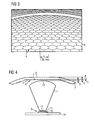
- the surface structure 4 with the pillow-shaped prominences 5 is shown in more detail in Figure 3 which shows an enlarged area of the second optical element 2.
- the pillow-shaped prominences 5 have hexagonal base areas.
- the pillow-shaped prominences 5 may also have octagonal or another type of a polygonal base areas.
- the lateral size L of the pillow-shaped prominences 5 is preferably between 200 ⁇ m and 5 mm. In the embodiment shown in Figure 3 the lateral size L of the pillow-shaped prominences is 1.00 mm.
- the height h of the pillow-shaped prominences 5 which is indicated in Figure 4 is preferably 200 ⁇ m or more. It is desirable that multiple internal reflections of the light beams occur in the second optical element. To obtain between 10 and 20 reflections inside the surface structure 4, a height of at least 500 ⁇ m is preferred for the pillow-shaped prominences 5.
- a surface structure 4 with a lateral pillow sizes of 1 mm, as shown in Figure 3 is a good choice for a light source with a comparatively narrow beam.
- the height h of the pillow-shaped prominences 5 should be at least between 200 ⁇ m and 500 ⁇ m to obtain a good colour mixing.
- the lateral dimensions L of the pillow-shaped prominences 5 should be about 2 mm.
- the optimum size of the pillow-shaped prominences 5 is related to the shape of the incoming beam at the light entrance surface 6. Furthermore, the size and the shape of the pillows is related to the amount of wavelength separation that is caused by the distribution of luminescence conversion material on the LED or by the distance between the LED chips which produce white light by colour mixing. It has been found out that an as small as possible surface structure 4 of pillow-shaped prominences 5 improves the wavelengths mixing and reduces in this way the effect of wavelengths separation due to the primary lens of the LED illumination system.
- the distance D between the light source 3 and the pillow-shaped surface structure 4 should be small to achieve a good wavelength mixing.
- the distance between the first optical element 1 and the surface structure 4 of the second optical element 2 is 2000 ⁇ m or less.
- the distance D can be in the range between 50 ⁇ m and 1500 ⁇ m.
- the second optical element can be advantageously comparatively thin.
- the overall height H of the second optical element 2 is in the range between 500 ⁇ m and 2500 ⁇ m. In a preferred embodiment, the overall height of the second optical element 2 is about 600 ⁇ m. In this case, the second optical element 2 has a high value of transmittance, for example in the range of 90 %.
- FIG. 5 A simulation of the light distribution behind the first optical element 1, as seen in the main direction, is presented in Figure 5 and a simulated light distribution behind the second optical element 2 is shown in Figure 6 .
- the light intensity in arbitrary units is calculated as a function of the vertical angle ⁇ v (curve 15) and the horizontal angle ⁇ h (curve 16) with respect to the main direction 9.
- the light distribution behind the second optical element 2 is a homogenous distribution with totally white colour.
- the beam divergence behind the second optical element 2 ( Fig. 6 ) is advantageously reduced in comparison to the beam divergence behind the first optical element ( Fig. 5 ). This results in a light distribution with a more narrow peak which is mainly due to the convex curvature of the light exit surface 7.
- the second optical element 2 with the surface structure 4 that comprises a plurality of pillow-shaped prominences 5 can advantageously be used in combination with any kind of primary lens that is used in combination with an LED light source when the optical wavelength separation is visible in the colour coordinates in a CIE diagram.
Abstract
Description
- The invention relates to an LED illumination system, in particular to an LED illumination system which emits white light.
- LED light sources are characterized by a high efficiency, a long lifetime and a comparatively low sensitivity against shocks and vibrations. Therefore LED light sources can be used in illumination systems in which incandescent lamps have often been used so far, in particular in lamps for general lighting or in car headlights. Due to their high brightness, LED light sources are also suited for use in traffic lamps or in light sources for projection systems.
- LED light sources are often used in combination with one or more optical elements which reduce the divergence of the emitted light. For example, the document
US 2004/0264185 A1 describes an LED light source that contains an optical concentrator to reduce the divergence of the emitted light. - The document
WO 98/12757 A1 - Another known method to produce white light with LED chips is colour mixing. In this case, the light emitted by a plurality of LED chips with different colours, for example red, green and blue light, is intermixed to white light. Both methods to produce white light by luminescence conversion or by colour mixing are based on the intermixing of light with at least two different wavelengths. In LED illumination devices which use one of these methods to produce white light the problem may occur that the intermixing of different colours to white light is not perfect. In this case, the light distribution does not show homogenous white light but unwanted colours in at least some directions in which light is emitted. This problem particularly occurs when an optical element, e.g. a primary lens or an optical concentrator, is used in combination with the LED light source.
- It is an object of the present invention to provide an improved LED illumination system, in particular an LED illumination system which provides an improved colour mixing to produce a homogenous light distribution, preferably of totally white colour.
- This object is achieved according to the invention by an LED illumination system according to
claim 1. Advantageous refinements of the invention are specified in the dependent claims. - According to the invention, an LED illumination system comprises an LED light source which emits light in a main direction, a first optical element and a second optical element which is arranged downstream of the first optical element in the main direction. The second optical element has on a light entrance surface which faces the LED light source a surface structure that comprises a plurality of pillow-shaped prominences.
- The pillow-shaped prominences which are arranged on the light entrance surface of the second optical element advantageously diffuse the light emitted by the LED light source after it has passed the first optical element. In this way, the pillow-shaped surface structure improves the colour mixing of the light that is emitted by the LED light source.
- Preferably, the second optical element has a convex curvature on the light exit surface which is opposite of the pillow-shaped surface structure. In this way, the light entrance surface of the second optical element diffuses the incoming light, whereas the light exit surface of the second optical element collimates the light beam.
- The pillow-shaped prominences preferably have a polygonal base area. In particular, the polygonal base area can be a hexagonal or an octagonal base area. In this way, it can be achieved that the base areas of the pillow-shaped prominences cover the complete light entrance surface of the second optical element. This is in particular advantageous in comparison to prominences with a circular or elliptical base area because in this case there would be regions between the prominences which have flat surfaces.
- The lateral size of the pillow-shaped prominences is advantageously between 200 µm and 5 mm.
- The surfaces of the pillow-shaped prominences preferably have a convex curvature. In particular, the convex curvature can be an elliptical curvature. The height of the pillow-shaped prominences is advantageously 200 µm or more. In a particularly preferred embodiment the height of the pillow-shaped prominences is 500 µm or more. In this case, multiple reflections of the light beams advantageously occur inside the pillow-shaped prominences. Preferably, the number of internal reflections of a light beam inside the pillow-shaped prominences is between 10 and 20.
- In a preferred embodiment of the invention a distance between a light exit surface of the first optical element and the light entrance surface of the second optical element is 2000 µm or less. In particular, the distance between the light exit surface of the first optical element and the light entrance surface of the second optical element can be between 50 µm and 1500 µm.
- In a preferred embodiment of the invention, the LED light source emits white light. However, the invention is not restricted to white light sources. In particular, the invention can also advantageously be used to improve the colour mixing of the colours of a plurality of LED chips to a combination colour.
- The LED light source comprises in a preferred embodiment at least one LED chip which emits ultraviolet and/or blue light. In this case, the LED illumination system advantageously comprises a luminescence conversion layer. The luminescence conversion layer might be arranged between the LED light source and the first optical element. For example, the luminescence conversion layer can be deposited on the at least one LED chip or on the light entrance surface of the first optical element. Alternatively, luminescence conversion particles can also be distributed in the first optical element. For example, the first optical element can be made of a polymer and the luminescence conversion particles can be embedded in the polymer.
- With the luminescence conversion layer, at least a part of the light that is emitted by the LED chips is converted to longer wavelengths, in particular to a complementary colour. The complementary colours are preferably mixed to white light. For example, blue light which is emitted from the LED chips and yellow light which is produced by the luminescence conversion particles are mixed to white light.
- In another preferred embodiment the LED light source comprises at least one red, one green and one blue LED chip to produce white light by colour mixing.
- In both cases of white light production by luminescence conversion and colour mixing, the mixing of the different wavelengths is improved by the pillow-shaped surface structure on the light entrance surface of the second optical element.
- In a preferred embodiment of the invention, the LED light source comprises a plurality of LED chips. For example, the LED light source can comprise a plurality of blue light emitting LED chips which emit light that is converted to white light.
- In another preferred embodiment the first optical element is an optical concentrator. In particular, the optical concentrator may be a compound parabolic concentrator (CPC). The optical concentrator advantageously reduces the divergence of the light that is emitted by the LED source.
- The invention is explained in more detail in the following description of preferred embodiments in connection with
Figures 1 to 6 in which: -
Figure 1 diagrammatically shows a cross-section through an LED illumination system according to a first embodiment of the invention, -
Figure 2 diagrammatically shows a top view and a bottom view of the second optical element according to an embodiment of the invention, -
Figure 3 diagrammatically shows an enlarged view of the second optical element which is shown inFigure 2 , -
Figure 4 diagrammatically shows a further cross-section through the LED illumination system according to the first embodiment of the invention, -
Figure 5 diagrammatically shows a simulated light distribution behind the first optical element, and -
Figure 6 diagrammatically shows a simulated light distribution behind the second optical element. - Identical or identically acting elements are provided with the same reference symbols in the Figures.
- The first embodiment of the invention which is shown in
Figure 1 comprises anLED light source 3 which emits light 8 in amain direction 9, a firstoptical element 1 and a secondoptical element 2 which is arranged downstream of the firstoptical element 1 in themain direction 9. - The LED
light source 3 comprises at least oneLED chip 10 which may be arranged on acarrier 14. Preferably, theLED chip 10 is an LED chip which emits blue or ultraviolet light. In this case, aluminescence conversion layer 11 is preferably arranged on the surface of theLED chip 10. Theluminescence conversion layer 11 contains luminescence conversion particles which are able to convert the emitted blue or ultraviolet light 8 to longer wavelengths, in particular to a complementary colour, e.g. yellow. Luminescence conversion particles which can be used are described for example in the documentWO 98/12757 A1 - The
luminescence conversion layer 11 is not necessarily placed on the top surface of theLED chip 10. Alternatively, theluminescence conversion layer 11 may be placed on alight entrance surface 12 or alight exit surface 13 of the firstoptical element 1. It is also possible that luminescence conversion particles are arranged inside the volume of the firstoptical element 1. For example, the firstoptical element 1 is made of a polymer, in particular polycarbonate, and the luminescence conversion particles may be embedded in the polymer. - Instead of one or more blue or ultraviolet light-emitting
LED chips 10 theLED light source 3 may also comprise at least one red, one green and one blue LED chip to produce white light by colour mixing. In this case, aluminescence conversion layer 11 is not necessary for the production of white light. - The first
optical element 1 is preferably used to reduce the beam divergence of the light 8 that is emitted by theLED chip 10. In particular, the firstoptical element 1 can be an optical concentrator. The light that is emitted by theLED chip 10 enters the optical concentrator at alight entrance surface 12 which is preferably arranged close to the light exit surface of theLED chip 10. Light beams which are emitted under comparatively large angles with respect to themain direction 9 are reflected at the side surfaces of theoptical concentrator 1 and are in this way directed to thelight exit surface 13 of theoptical concentrator 1. - The first
optical element 1 reduces the beam divergence of the emitted light 8. However, the colour mixing may not be perfect behind the firstoptical element 1. This means that there may be a local variation of the colour of the emitted light after it has passed the optical concentrator. In particular, the coordinates of the light in a CIE diagram can vary in a plane above thelight exit surface 13 of theoptical concentrator 1. - To improve the colour mixing the LED illumination system comprises a second
optical element 2. The refractive index of the second optical element is preferably in a range between 1 and 1.8. In particular, the material of the secondoptical element 2 can be a polymer. In this case, the secondoptical element 2 can be produced by injection moulding with low effort. - The second
optical element 2 has asurface structure 4 on alight entrance surface 6 which faces theLED light source 3. Thesurface structure 4 comprises a plurality of pillow-shapedprominences 5. The pillow-shapedprominences 5 preferably have a polygonal base area and a convex curved surface. For example, the convex-shaped surface of theprominences 5 may have an ellipsoidal or a spherical curvature. Alternatively, the pillow-shapedprominences 5 may also have a pyramidal structure. The optimum curvature of the pillow-shapedprominences 5 depends on the desired collimation angle. It can be found out by an optical simulation of the light distribution behind the first and second optical element. - A second
optical element 2 according to an embodiment of the invention is shown inFigure 2 in a perspective top view (left side) and in a perspective bottom view (right side). Thelight exit surface 7 on the top side of the secondoptical element 2 has a convex curvature to collimate the light beam. Thelight entrance surface 6 which is arranged on the bottom side of the secondoptical element 2 has asurface structure 4 that comprises a plurality of pillow-shapedprominences 5. - The
surface structure 4 with the pillow-shapedprominences 5 is shown in more detail inFigure 3 which shows an enlarged area of the secondoptical element 2. The pillow-shapedprominences 5 have hexagonal base areas. Alternatively, the pillow-shapedprominences 5 may also have octagonal or another type of a polygonal base areas. - The lateral size L of the pillow-shaped
prominences 5 is preferably between 200 µm and 5 mm. In the embodiment shown inFigure 3 the lateral size L of the pillow-shaped prominences is 1.00 mm. - The height h of the pillow-shaped
prominences 5 which is indicated inFigure 4 is preferably 200 µm or more. It is desirable that multiple internal reflections of the light beams occur in the second optical element. To obtain between 10 and 20 reflections inside thesurface structure 4, a height of at least 500 µm is preferred for the pillow-shapedprominences 5. - A
surface structure 4 with a lateral pillow sizes of 1 mm, as shown inFigure 3 , is a good choice for a light source with a comparatively narrow beam. In this case, the height h of the pillow-shapedprominences 5 should be at least between 200 µm and 500 µm to obtain a good colour mixing. - For a light source with a broad beam, in particular for a light source with a Lambertian radiation pattern, the lateral dimensions L of the pillow-shaped
prominences 5 should be about 2 mm. - The optimum size of the pillow-shaped
prominences 5 is related to the shape of the incoming beam at thelight entrance surface 6. Furthermore, the size and the shape of the pillows is related to the amount of wavelength separation that is caused by the distribution of luminescence conversion material on the LED or by the distance between the LED chips which produce white light by colour mixing. It has been found out that an as small aspossible surface structure 4 of pillow-shapedprominences 5 improves the wavelengths mixing and reduces in this way the effect of wavelengths separation due to the primary lens of the LED illumination system. - The distance D between the
light source 3 and the pillow-shapedsurface structure 4 should be small to achieve a good wavelength mixing. Preferably, the distance between the firstoptical element 1 and thesurface structure 4 of the secondoptical element 2 is 2000 µm or less. In particular, the distance D can be in the range between 50 µm and 1500 µm. - The second optical element can be advantageously comparatively thin. In particular, the overall height H of the second
optical element 2 is in the range between 500 µm and 2500 µm. In a preferred embodiment, the overall height of the secondoptical element 2 is about 600 µm. In this case, the secondoptical element 2 has a high value of transmittance, for example in the range of 90 %. - A simulation of the light distribution behind the first
optical element 1, as seen in the main direction, is presented inFigure 5 and a simulated light distribution behind the secondoptical element 2 is shown inFigure 6 . In both cases, the light intensity in arbitrary units is calculated as a function of the vertical angle αv (curve 15) and the horizontal angle αh (curve 16) with respect to themain direction 9. It has been found out that the light distribution behind the secondoptical element 2 is a homogenous distribution with totally white colour. The beam divergence behind the second optical element 2 (Fig. 6 ) is advantageously reduced in comparison to the beam divergence behind the first optical element (Fig. 5 ). This results in a light distribution with a more narrow peak which is mainly due to the convex curvature of thelight exit surface 7. - The second
optical element 2 with thesurface structure 4 that comprises a plurality of pillow-shapedprominences 5 can advantageously be used in combination with any kind of primary lens that is used in combination with an LED light source when the optical wavelength separation is visible in the colour coordinates in a CIE diagram. - The scope of protection of the invention is not limited to the examples given hereinabove. The invention is embodied in each novel characteristic and each combination of characteristics, which particularly includes every combination of any features which are stated in the claims, even if this feature or this combination of features is not explicitly stated in the claims or in the examples.
Claims (17)
- An LED illumination system comprising an LED light source (3) which emits light (8) in a main direction (9) and a first optical element (1),
wherein a second optical element (2) is arranged downstream of the first optical element (1) in the main direction (9), and the second optical element (2) has on a light entrance surface (6) which faces the LED light source (3) a surface structure (4) that comprises a plurality of pillow-shaped prominences (5). - An LED illumination system according to claim 1,
wherein a light exit surface (7) of the second optical element (2) has a convex curvature. - An LED illumination system according to claim 1,
wherein the pillow-shaped prominences (5) have a polygonal base area. - An LED illumination system according to claim 2,
wherein the polygonal base area is a hexagonal or an octagonal base area. - An LED illumination system according to one of the preceding claims,
wherein a lateral size L of the pillow-shaped prominences (5) is between 200 µm and 5 mm. - An LED illumination system according to one of the preceding claims,
wherein the surfaces of the pillow-shaped prominences (5) have a convex curvature. - An LED illumination system according to claim 6,
wherein the convex curvature is an elliptical curvature. - An LED illumination system according to one of the preceding claims,
wherein a height h of the pillow-shaped prominences (5) is 200 µm or more. - An LED illumination system according to one of the preceding claims,
wherein a distance D between a light exit surface of the first optical element (1) and the light entrance surface (6) of the second optical element (2) is 2000 µm or less. - An LED illumination system according to claim 9,
wherein the distance D is between 50 µm and 1500 µm. - An LED illumination system according to one of the preceding claims,
wherein the LED light source (3) emits white light. - An LED illumination system according to one of the preceding claims,
wherein the LED light source (3) comprises at least one LED chip (10) which emits ultraviolet and/or blue light. - An LED illumination system according to claim 12,
which comprises a luminescence conversion layer (11). - An LED illumination system according to one of claims 1 to 11,
wherein the LED light source comprises at least one red, one green and one blue LED chip to produce white light by colour mixing. - An LED illumination system according to one of the preceding claims,
wherein the LED light source (3) comprises a plurality of LED chips. - An LED illumination system according to one of the preceding claims,
wherein the first optical element (1) is an optical concentrator. - An LED illumination system according to claim 16,
wherein the optical concentrator (1) is a compound parabolic concentrator.
Priority Applications (2)
| Application Number | Priority Date | Filing Date | Title |
|---|---|---|---|
| EP06024400.1A EP1925874B8 (en) | 2006-11-24 | 2006-11-24 | LED color-mixing lighting system |
| US11/986,806 US7780317B2 (en) | 2006-11-24 | 2007-11-26 | LED illumination system |
Applications Claiming Priority (1)
| Application Number | Priority Date | Filing Date | Title |
|---|---|---|---|
| EP06024400.1A EP1925874B8 (en) | 2006-11-24 | 2006-11-24 | LED color-mixing lighting system |
Publications (3)
| Publication Number | Publication Date |
|---|---|
| EP1925874A1 true EP1925874A1 (en) | 2008-05-28 |
| EP1925874B1 EP1925874B1 (en) | 2014-08-06 |
| EP1925874B8 EP1925874B8 (en) | 2014-09-10 |
Family
ID=37907511
Family Applications (1)
| Application Number | Title | Priority Date | Filing Date |
|---|---|---|---|
| EP06024400.1A Active EP1925874B8 (en) | 2006-11-24 | 2006-11-24 | LED color-mixing lighting system |
Country Status (2)
| Country | Link |
|---|---|
| US (1) | US7780317B2 (en) |
| EP (1) | EP1925874B8 (en) |
Cited By (10)
| Publication number | Priority date | Publication date | Assignee | Title |
|---|---|---|---|---|
| WO2013130606A3 (en) * | 2012-02-29 | 2013-10-24 | Sabic Innovative Plastics Ip B.V. | Process for producing low sulfur bisphenol a, processes for producing polycarbonate, articles made from polycarbonate |
| US8962117B2 (en) | 2011-10-27 | 2015-02-24 | Sabic Global Technologies B.V. | Process for producing bisphenol A with reduced sulfur content, polycarbonate made from the bisphenol A, and containers formed from the polycarbonate |
| US9006378B2 (en) | 2013-05-29 | 2015-04-14 | Sabic Global Technologies B.V. | Color stable thermoplastic composition |
| US9287471B2 (en) | 2012-02-29 | 2016-03-15 | Sabic Global Technologies B.V. | Polycarbonate compositions containing conversion material chemistry and having enhanced optical properties, methods of making and articles comprising the same |
| US9290618B2 (en) | 2011-08-05 | 2016-03-22 | Sabic Global Technologies B.V. | Polycarbonate compositions having enhanced optical properties, methods of making and articles comprising the polycarbonate compositions |
| US9346949B2 (en) | 2013-02-12 | 2016-05-24 | Sabic Global Technologies B.V. | High reflectance polycarbonate |
| US9490405B2 (en) | 2012-02-03 | 2016-11-08 | Sabic Innovative Plastics Ip B.V. | Light emitting diode device and method for production thereof containing conversion material chemistry |
| US9553244B2 (en) | 2013-05-16 | 2017-01-24 | Sabic Global Technologies B.V. | Branched polycarbonate compositions having conversion material chemistry and articles thereof |
| US9772086B2 (en) | 2013-05-29 | 2017-09-26 | Sabic Innovative Plastics Ip B.V. | Illuminating devices with color stable thermoplastic light transmitting articles |
| US9821523B2 (en) | 2012-10-25 | 2017-11-21 | Sabic Global Technologies B.V. | Light emitting diode devices, method of manufacture, uses thereof |
Families Citing this family (14)
| Publication number | Priority date | Publication date | Assignee | Title |
|---|---|---|---|---|
| CA2640913C (en) | 2007-10-12 | 2017-05-09 | The L.D. Kichler Co. | Positionable lighting systems and methods |
| KR100998017B1 (en) * | 2009-02-23 | 2010-12-03 | 삼성엘이디 주식회사 | Lens for Light Emitting Diode Package and Light Emitting Diode Package Having The Same |
| DE102009049057B4 (en) * | 2009-10-12 | 2018-10-25 | Osram Gmbh | LED module, method of operating this LED module and lighting device with this LED module |
| KR101216084B1 (en) | 2010-06-23 | 2012-12-26 | 엘지전자 주식회사 | Lighting device and module type lighting device |
| KR101053633B1 (en) | 2010-06-23 | 2011-08-03 | 엘지전자 주식회사 | Module type lighting device |
| KR101057064B1 (en) * | 2010-06-30 | 2011-08-16 | 엘지전자 주식회사 | Led based lamp and method for manufacturing the same |
| KR101053634B1 (en) | 2010-07-02 | 2011-08-03 | 엘지전자 주식회사 | Led based lamp and method for manufacturing the same |
| US20130286653A1 (en) * | 2012-04-30 | 2013-10-31 | Qualcomm Mems Technologies, Inc. | Multi-beam light engine |
| US9890938B2 (en) | 2016-02-08 | 2018-02-13 | Gemmy Industries Corp. | Decorative light |
| US10400966B2 (en) | 2013-12-31 | 2019-09-03 | Gemmy Industries Corp. | Decorative lights and related methods |
| DE102016119711B4 (en) * | 2015-10-20 | 2023-08-31 | Panasonic Intellectual Property Management Co., Ltd. | lighting device |
| USD791381S1 (en) | 2016-02-08 | 2017-07-04 | Gemmy Industries Corp. | Decorative light |
| US10234118B2 (en) | 2016-02-08 | 2019-03-19 | Gemmy Industries Corp. | Decorative light |
| CZ2020667A3 (en) * | 2020-12-10 | 2022-01-26 | Crytur, Spol. S.R.O. | Light source |
Citations (7)
| Publication number | Priority date | Publication date | Assignee | Title |
|---|---|---|---|---|
| WO1998012757A1 (en) | 1996-09-20 | 1998-03-26 | Siemens Aktiengesellschaft | Sealing material with wavelength converting effect, application and production process |
| US20040264185A1 (en) | 2003-04-29 | 2004-12-30 | Osram Opto Semiconductors Gmbh | Light source |
| WO2005022030A2 (en) * | 2003-08-29 | 2005-03-10 | Koninklijke Philips Electronics N.V. | Color-mixing lighting system |
| EP1533774A1 (en) | 2003-11-19 | 2005-05-25 | Dialight Garufo GmbH | Signal lamp |
| US20060027828A1 (en) * | 2004-08-06 | 2006-02-09 | Citizen Electronics Co., Ltd. | Light-emitting diode lamp |
| WO2006072398A1 (en) * | 2005-01-05 | 2006-07-13 | Hansa Metallwerke Ag | Sanitary fitting comprising an assembly of light-emitting elements |
| DE102005059362A1 (en) * | 2005-02-01 | 2006-09-07 | Helmut Dipl.-Ing. Grantz | Adjustable color daylight source has at least one light emitting diode emitting white light of defined color temperature combined with light emitting diodes emitting light of least two different colors |
Family Cites Families (6)
| Publication number | Priority date | Publication date | Assignee | Title |
|---|---|---|---|---|
| US5442252A (en) * | 1992-11-16 | 1995-08-15 | General Electric Company | Lenticulated lens with improved light distribution |
| US6086227A (en) * | 1998-09-11 | 2000-07-11 | Osram Sylvania Inc. | Lamp with faceted reflector and spiral lens |
| US6953264B2 (en) * | 2000-12-02 | 2005-10-11 | American Superlite, Inc. | Vehicle light assembly |
| US7196460B2 (en) * | 2004-07-01 | 2007-03-27 | Osram Sylvania Inc. | Incandescent reflector heat lamp with uniform irradiance |
| KR101080355B1 (en) * | 2004-10-18 | 2011-11-04 | 삼성전자주식회사 | Light emitting diode, lens for the same |
| WO2007121486A2 (en) * | 2006-04-18 | 2007-10-25 | Lamina Lighting, Inc. | Optical devices for controlled color mixing |
-
2006
- 2006-11-24 EP EP06024400.1A patent/EP1925874B8/en active Active
-
2007
- 2007-11-26 US US11/986,806 patent/US7780317B2/en active Active
Patent Citations (7)
| Publication number | Priority date | Publication date | Assignee | Title |
|---|---|---|---|---|
| WO1998012757A1 (en) | 1996-09-20 | 1998-03-26 | Siemens Aktiengesellschaft | Sealing material with wavelength converting effect, application and production process |
| US20040264185A1 (en) | 2003-04-29 | 2004-12-30 | Osram Opto Semiconductors Gmbh | Light source |
| WO2005022030A2 (en) * | 2003-08-29 | 2005-03-10 | Koninklijke Philips Electronics N.V. | Color-mixing lighting system |
| EP1533774A1 (en) | 2003-11-19 | 2005-05-25 | Dialight Garufo GmbH | Signal lamp |
| US20060027828A1 (en) * | 2004-08-06 | 2006-02-09 | Citizen Electronics Co., Ltd. | Light-emitting diode lamp |
| WO2006072398A1 (en) * | 2005-01-05 | 2006-07-13 | Hansa Metallwerke Ag | Sanitary fitting comprising an assembly of light-emitting elements |
| DE102005059362A1 (en) * | 2005-02-01 | 2006-09-07 | Helmut Dipl.-Ing. Grantz | Adjustable color daylight source has at least one light emitting diode emitting white light of defined color temperature combined with light emitting diodes emitting light of least two different colors |
Non-Patent Citations (1)
| Title |
|---|
| SCHREIBER, P.: "Homogeneous LED-illumination using microlens arrays", NONIMAGING OPTICS AND EFFICIENT ILLUMINATION SYSTEMS II, vol. 5942, 20 August 2005 (2005-08-20), XP002429677 * |
Cited By (14)
| Publication number | Priority date | Publication date | Assignee | Title |
|---|---|---|---|---|
| US9957351B2 (en) | 2011-08-05 | 2018-05-01 | Sabic Global Technologies B.V. | Polycarbonate compositions having enhanced optical properties, methods of making and articles comprising the polycarbonate compositions |
| US9290618B2 (en) | 2011-08-05 | 2016-03-22 | Sabic Global Technologies B.V. | Polycarbonate compositions having enhanced optical properties, methods of making and articles comprising the polycarbonate compositions |
| US8962117B2 (en) | 2011-10-27 | 2015-02-24 | Sabic Global Technologies B.V. | Process for producing bisphenol A with reduced sulfur content, polycarbonate made from the bisphenol A, and containers formed from the polycarbonate |
| US9490405B2 (en) | 2012-02-03 | 2016-11-08 | Sabic Innovative Plastics Ip B.V. | Light emitting diode device and method for production thereof containing conversion material chemistry |
| US9711695B2 (en) | 2012-02-03 | 2017-07-18 | Sabic Global Technologies B.V. | Light emitting diode device and method for production thereof containing conversion material chemistry |
| US9287471B2 (en) | 2012-02-29 | 2016-03-15 | Sabic Global Technologies B.V. | Polycarbonate compositions containing conversion material chemistry and having enhanced optical properties, methods of making and articles comprising the same |
| US9299898B2 (en) | 2012-02-29 | 2016-03-29 | Sabic Global Technologies B.V. | Polycarbonate compositions containing conversion material chemistry and having enhanced optical properties, methods of making and articles comprising the same |
| WO2013130606A3 (en) * | 2012-02-29 | 2013-10-24 | Sabic Innovative Plastics Ip B.V. | Process for producing low sulfur bisphenol a, processes for producing polycarbonate, articles made from polycarbonate |
| US9771452B2 (en) | 2012-02-29 | 2017-09-26 | Sabic Global Technologies B.V. | Plastic composition comprising a polycarbonate made from low sulfur bisphenol A, and articles made therefrom |
| US9821523B2 (en) | 2012-10-25 | 2017-11-21 | Sabic Global Technologies B.V. | Light emitting diode devices, method of manufacture, uses thereof |
| US9346949B2 (en) | 2013-02-12 | 2016-05-24 | Sabic Global Technologies B.V. | High reflectance polycarbonate |
| US9553244B2 (en) | 2013-05-16 | 2017-01-24 | Sabic Global Technologies B.V. | Branched polycarbonate compositions having conversion material chemistry and articles thereof |
| US9772086B2 (en) | 2013-05-29 | 2017-09-26 | Sabic Innovative Plastics Ip B.V. | Illuminating devices with color stable thermoplastic light transmitting articles |
| US9006378B2 (en) | 2013-05-29 | 2015-04-14 | Sabic Global Technologies B.V. | Color stable thermoplastic composition |
Also Published As
| Publication number | Publication date |
|---|---|
| US20080123331A1 (en) | 2008-05-29 |
| EP1925874B8 (en) | 2014-09-10 |
| US7780317B2 (en) | 2010-08-24 |
| EP1925874B1 (en) | 2014-08-06 |
Similar Documents
| Publication | Publication Date | Title |
|---|---|---|
| EP1925874B1 (en) | LED color-mixing lighting system | |
| JP6006547B2 (en) | LIGHTING DEVICE AND LENS SHEET USED FOR THE SAME | |
| KR101212911B1 (en) | Lighting module and luminaire | |
| US7581860B2 (en) | Headlight and headlight element | |
| US7401947B2 (en) | Lighting means having a primary optics element and an optical apparatus | |
| US9097824B2 (en) | Light mixing module, and a luminaire comprising such a light mixing module | |
| EP2476943B1 (en) | Flat LED lighting device | |
| KR20100084468A (en) | Light source | |
| US20090046459A1 (en) | Lighting device | |
| US20110163334A1 (en) | Colour mixing method for consistent colour quality | |
| US10845026B2 (en) | Lighting device including a transparent structure with groups of diffusing lenslets on an emission surface having a different aspect ratio | |
| JP2010192439A (en) | Light emitting device and light guide member for the same | |
| EP2721656B1 (en) | Led light source | |
| US10288261B2 (en) | Low profile lighting module | |
| US8403538B2 (en) | Color homogenizing optical assembly | |
| KR20160101093A (en) | Led module with uniform phosphor illumination | |
| EP3078903B1 (en) | Lighting module | |
| EP2726780B1 (en) | Light guide | |
| US7217010B2 (en) | Reflector with negative focal length | |
| JP2013045530A (en) | Light emitting device and lighting fixture | |
| US8894250B2 (en) | Illuminating device | |
| JP5473966B2 (en) | Light source unit and lighting device | |
| CN111503534B (en) | LED illuminator | |
| JP2014135322A (en) | Light emitting device and luminaire | |
| TWI579504B (en) | Light emitting device |
Legal Events
| Date | Code | Title | Description |
|---|---|---|---|
| PUAI | Public reference made under article 153(3) epc to a published international application that has entered the european phase |
Free format text: ORIGINAL CODE: 0009012 |
|
| AK | Designated contracting states |
Kind code of ref document: A1 Designated state(s): AT BE BG CH CY CZ DE DK EE ES FI FR GB GR HU IE IS IT LI LT LU LV MC NL PL PT RO SE SI SK TR |
|
| AX | Request for extension of the european patent |
Extension state: AL BA HR MK RS |
|
| 17P | Request for examination filed |
Effective date: 20081029 |
|
| 17Q | First examination report despatched |
Effective date: 20081121 |
|
| AKX | Designation fees paid |
Designated state(s): DE IT |
|
| R17C | First examination report despatched (corrected) |
Effective date: 20081127 |
|
| REG | Reference to a national code |
Ref country code: DE Ref legal event code: R079 Ref document number: 602006042568 Country of ref document: DE Free format text: PREVIOUS MAIN CLASS: F21K0007000000 Ipc: F21K0099000000 |
|
| GRAP | Despatch of communication of intention to grant a patent |
Free format text: ORIGINAL CODE: EPIDOSNIGR1 |
|
| RIC1 | Information provided on ipc code assigned before grant |
Ipc: F21V 7/00 20060101ALI20140110BHEP Ipc: F21K 99/00 20100101AFI20140110BHEP Ipc: F21Y 101/02 20060101ALN20140110BHEP Ipc: F21V 5/00 20060101ALI20140110BHEP |
|
| INTG | Intention to grant announced |
Effective date: 20140211 |
|
| GRAS | Grant fee paid |
Free format text: ORIGINAL CODE: EPIDOSNIGR3 |
|
| GRAA | (expected) grant |
Free format text: ORIGINAL CODE: 0009210 |
|
| AK | Designated contracting states |
Kind code of ref document: B1 Designated state(s): DE IT |
|
| RAP2 | Party data changed (patent owner data changed or rights of a patent transferred) |
Owner name: OSRAM GMBH Owner name: OSRAM S.P.A. - SOCIETA' RIUNITE OSRAM EDISON CLERI |
|
| REG | Reference to a national code |
Ref country code: DE Ref legal event code: R096 Ref document number: 602006042568 Country of ref document: DE Effective date: 20140918 |
|
| REG | Reference to a national code |
Ref country code: DE Ref legal event code: R097 Ref document number: 602006042568 Country of ref document: DE |
|
| PLBE | No opposition filed within time limit |
Free format text: ORIGINAL CODE: 0009261 |
|
| STAA | Information on the status of an ep patent application or granted ep patent |
Free format text: STATUS: NO OPPOSITION FILED WITHIN TIME LIMIT |
|
| 26N | No opposition filed |
Effective date: 20150507 |
|
| PGFP | Annual fee paid to national office [announced via postgrant information from national office to epo] |
Ref country code: IT Payment date: 20181126 Year of fee payment: 13 |
|
| PG25 | Lapsed in a contracting state [announced via postgrant information from national office to epo] |
Ref country code: IT Free format text: LAPSE BECAUSE OF NON-PAYMENT OF DUE FEES Effective date: 20191124 |
|
| REG | Reference to a national code |
Ref country code: DE Ref legal event code: R081 Ref document number: 602006042568 Country of ref document: DE Owner name: OPTOTRONIC GMBH, DE Free format text: FORMER OWNER: OSRAM GMBH, 80807 MUENCHEN, DE Ref country code: DE Ref legal event code: R082 Ref document number: 602006042568 Country of ref document: DE |
|
| PGFP | Annual fee paid to national office [announced via postgrant information from national office to epo] |
Ref country code: DE Payment date: 20231120 Year of fee payment: 18 |