EP1931133A1 - Method and device for optical acquisition of a structure - Google Patents
Method and device for optical acquisition of a structure Download PDFInfo
- Publication number
- EP1931133A1 EP1931133A1 EP07119614A EP07119614A EP1931133A1 EP 1931133 A1 EP1931133 A1 EP 1931133A1 EP 07119614 A EP07119614 A EP 07119614A EP 07119614 A EP07119614 A EP 07119614A EP 1931133 A1 EP1931133 A1 EP 1931133A1
- Authority
- EP
- European Patent Office
- Prior art keywords
- image
- optical element
- images
- image sensor
- imaging
- Prior art date
- Legal status (The legal status is an assumption and is not a legal conclusion. Google has not performed a legal analysis and makes no representation as to the accuracy of the status listed.)
- Withdrawn
Links
- 230000003287 optical effect Effects 0.000 title claims abstract description 62
- 238000000034 method Methods 0.000 title claims abstract description 13
- 238000001514 detection method Methods 0.000 claims abstract description 12
- 230000005693 optoelectronics Effects 0.000 claims abstract 2
- 238000003384 imaging method Methods 0.000 claims description 46
- 238000011156 evaluation Methods 0.000 claims description 7
- 238000012544 monitoring process Methods 0.000 description 15
- 239000011159 matrix material Substances 0.000 description 5
- 230000002238 attenuated effect Effects 0.000 description 4
- 238000013507 mapping Methods 0.000 description 4
- 230000015572 biosynthetic process Effects 0.000 description 3
- 238000005286 illumination Methods 0.000 description 2
- 208000027418 Wounds and injury Diseases 0.000 description 1
- 230000005540 biological transmission Effects 0.000 description 1
- 239000006059 cover glass Substances 0.000 description 1
- 230000006378 damage Effects 0.000 description 1
- 230000003247 decreasing effect Effects 0.000 description 1
- 230000002950 deficient Effects 0.000 description 1
- 230000001419 dependent effect Effects 0.000 description 1
- 238000013461 design Methods 0.000 description 1
- 238000010586 diagram Methods 0.000 description 1
- 238000006073 displacement reaction Methods 0.000 description 1
- 230000009977 dual effect Effects 0.000 description 1
- 230000002349 favourable effect Effects 0.000 description 1
- 238000010191 image analysis Methods 0.000 description 1
- 238000001746 injection moulding Methods 0.000 description 1
- 208000014674 injury Diseases 0.000 description 1
- 239000000463 material Substances 0.000 description 1
- 238000012986 modification Methods 0.000 description 1
- 230000004048 modification Effects 0.000 description 1
- 239000013307 optical fiber Substances 0.000 description 1
- 230000010363 phase shift Effects 0.000 description 1
- 239000013589 supplement Substances 0.000 description 1
- 238000012360 testing method Methods 0.000 description 1
Images


Classifications
-
- H—ELECTRICITY
- H01—ELECTRIC ELEMENTS
- H01L—SEMICONDUCTOR DEVICES NOT COVERED BY CLASS H10
- H01L27/00—Devices consisting of a plurality of semiconductor or other solid-state components formed in or on a common substrate
- H01L27/14—Devices consisting of a plurality of semiconductor or other solid-state components formed in or on a common substrate including semiconductor components sensitive to infrared radiation, light, electromagnetic radiation of shorter wavelength or corpuscular radiation and specially adapted either for the conversion of the energy of such radiation into electrical energy or for the control of electrical energy by such radiation
- H01L27/144—Devices controlled by radiation
- H01L27/146—Imager structures
- H01L27/14601—Structural or functional details thereof
- H01L27/14625—Optical elements or arrangements associated with the device
-
- H—ELECTRICITY
- H04—ELECTRIC COMMUNICATION TECHNIQUE
- H04N—PICTORIAL COMMUNICATION, e.g. TELEVISION
- H04N23/00—Cameras or camera modules comprising electronic image sensors; Control thereof
- H04N23/58—Means for changing the camera field of view without moving the camera body, e.g. nutating or panning of optics or image sensors
-
- H—ELECTRICITY
- H01—ELECTRIC ELEMENTS
- H01L—SEMICONDUCTOR DEVICES NOT COVERED BY CLASS H10
- H01L27/00—Devices consisting of a plurality of semiconductor or other solid-state components formed in or on a common substrate
- H01L27/14—Devices consisting of a plurality of semiconductor or other solid-state components formed in or on a common substrate including semiconductor components sensitive to infrared radiation, light, electromagnetic radiation of shorter wavelength or corpuscular radiation and specially adapted either for the conversion of the energy of such radiation into electrical energy or for the control of electrical energy by such radiation
- H01L27/144—Devices controlled by radiation
- H01L27/146—Imager structures
- H01L27/14643—Photodiode arrays; MOS imagers
-
- H—ELECTRICITY
- H01—ELECTRIC ELEMENTS
- H01L—SEMICONDUCTOR DEVICES NOT COVERED BY CLASS H10
- H01L27/00—Devices consisting of a plurality of semiconductor or other solid-state components formed in or on a common substrate
- H01L27/14—Devices consisting of a plurality of semiconductor or other solid-state components formed in or on a common substrate including semiconductor components sensitive to infrared radiation, light, electromagnetic radiation of shorter wavelength or corpuscular radiation and specially adapted either for the conversion of the energy of such radiation into electrical energy or for the control of electrical energy by such radiation
- H01L27/144—Devices controlled by radiation
- H01L27/146—Imager structures
- H01L27/148—Charge coupled imagers
Definitions
- the invention relates to a method for optical detection of a structure according to the preamble of patent claim 1 and to a device for optically detecting a structure according to the preamble of patent claim 8.
- CMOS sensors can be made with better dynamics, but are more expensive and have a less favorable signal-to-noise ratio.
- the invention is based on the object to form the optical detection of structures more cost effective and reliable.
- the invention is based on the idea that when detecting a structure with a square or rectangular image sensor, in most cases, and in particular in elongated structures, only a small part of the sensor surface of the image sensor is utilized for imaging the structure, while a substantial part of the structure is used Sensor surface remains unused. Therefore, according to the invention, the matrix surface of a particularly square or rectangular image sensor for the detection of a structure is exploited by inserting into the imaging beam path of the camera system an optical element which images the structure into at least two regions of the image recorder which are separated from each other and offset from one another.
- the optical element preferably produces an image the structure in at least two areas which extend in the X-axis and are offset from each other in the Y-axis perpendicular to this.
- This makes it possible to take advantage of a larger part of the sensor surface or optionally also the entire sensor surface of a square or rectangular image sensor in the image of an elongated structure.
- the same image recorder can be optimally adapted to the respective task, ie the same hardware can be used more versatile.
- the entire structure is imaged on the image sensor in the two staggered areas. Although this does not improve the resolution, it does give a redundant image. If individual pixels (pixels) fail in one of the images, then these defective pixels of an image can be supplemented by the corresponding pixels of the offset second image.
- the multiple redundant mapping of the entire structure thus results in a two-channel monitoring with only one image sensor, so that the reliability of the two-channel monitoring is realized in a cost effective manner.
- the entire structure is also imaged in a region of the image recorder.
- the at least one other matching image of the entire structure is imaged in a separate area so as to be offset by a sub-pixel distance from the pitch of the pixels in the array of the imager compared to the first image.
- the offset of the image thus deviates from an integer multiple of the pixel spacing of the image recorder.
- the images of the same structure staggered by this subpixel spacing can then be used in the evaluation to mathematically improve the pixel resolution of the image.
- the utilization of the entire sensor surface can be used to improve the resolution of the image of an elongate structure.
- the image of the elongated structure in its longitudinal extent (X-axis) is divided into individual sections, which are shown offset from one another in the Y-axis.
- the longitudinal extent in the X-axis is less than the image of the entire structure, without thereby reducing the image resolution.
- the dynamic range of the image sensor can be extended.
- the entire structure is imaged in a surface area of the image recorder and the same structure is in each case also imaged in at least one separate and offset area.
- the light intensity of the exposure of the image sensor in the staggered areas is optically attenuated to different degrees.
- a large portion of the original illumination intensity of the structure in the different staggered areas can be gradually attenuated, so that in each case in at least one of these areas, the incident on the imager illumination intensity falls within the optimal dynamic range of the image sensor.
- one or more further offset regions with greater attenuation can be used to detect and supplement these points of the structure which are overdriven in the first region ,
- the detection according to the invention of a structure for securing a source of danger in a spatial area in which the structure is monitored for changes in order to detect impermissible object interventions in the spatial area and, if necessary, to secure a source of danger.
- a safety-related application not only the advantages of the improved utilization of the image sensor come into play, but it can also meet the requirement of redundant evaluation without additional hardware if required by the application in addition by multiple imaging of the whole structure or each multiple mapping of sections of the structure ,
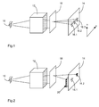
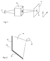
- FIG. 11 For illustration, a prior art camera system for detecting a structure is shown.
- the structure 10 is shown schematically as an arrow, but may be any structure, in particular an elongated structure, the extent of which in a longitudinal direction (X axis) is greater than its width in the Y axis perpendicular thereto.
- the structure 10 is detected by a camera system which has an imaging optics 12 which images the structure 10 onto an image recorder 14.
- the image sensor 14 is for example a CCD sensor or a CMOS sensor with a square or rectangular matrix of pixels.
- the structure 10 is imaged on the imager 14 as an image 16 corresponding to the structure 10. In general, the image 16 will occupy only a portion of the sensor surface of the image sensor 14, so that only this portion of the image sensor 14 is utilized.
- the image 16 utilizes only a stripe-shaped region of the image receptor 14 that extends in the X-axis.
- the imaging optics 12 can enlarge or reduce the image 16 in its longitudinal extension in the X-axis optimally exploits the dimensions of the image sensor 14 in this X-axis.
- the areas of the image sensor 14 on both sides of the image 16 remain unused.
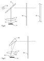
- FIG. 12 shows a typical example of the use of the detection of an elongated structure 10 for monitoring a field of view 24.
- a camera 26 is arranged in a space to monitor the field of view 24 between the camera 26 and the opposite walls 28 of the room.
- a retroreflective tape 22 is attached on the walls 28, a retroreflective tape 22 is attached.
- a light source arranged in the camera 26 illuminates the retroreflector belt 22, while the imaging optics of the camera 26 images the structure of the retroreflector belt 22 on the image recorder of the camera 26.
- the retroreflective belt 22 is elongated in one direction while being narrow in the direction perpendicular thereto. Accordingly, the image of the structure of the retroreflective tape 22 is elongate. Changes in the image of the structure of the retroreflector belt 22 on the image sensor of the camera 26 are detected as a disturbance of the monitored field of view 24 in order to trigger a corresponding signal.
- the camera 26 may also be a distance-resolving camera, for example by a light transmitter, not shown, which emits light pulses or modulated light, wherein the light transit time or the phase shift for determining distances is determined.
- a light transmitter not shown
- active or passive triangulation can be used to determine range values.
- the monitoring of the field of view 24 is carried out in a particularly preferred safety application for monitoring a source of danger, not shown.
- This may be a press, a fire, a cutting edge or any conceivable source of injury, in particular for operating personnel.
- an evaluation connected to or integrated into the camera 26 detects an inadmissible, ie unexpected object intervention, for example by comparison with a reference scene or sequence in the field of view 24 of permitted objects, then it switches an output which triggers an alarm or immediately switches off or off security command generated to the source of danger, so that it is switched off or otherwise brought to a safe state.
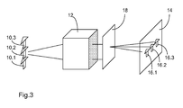
- FIGS. 1 to 9 are shown in schematic representation embodiments of the invention. As far as these statements with the prior art according to FIGS. 11 and 12 match, the same reference numerals are used.
- An optical element 18 is inserted into the imaging beam path of the camera system.
- the optical element 18 serves to deflect the imaging beams into different regions of the image sensor 14.
- the optical element 18 can be designed in different ways, as will be described in detail later.
- the optical element 18 can be arranged in front of the imaging optics 12 or between the imaging optics 12 and the image recorder 14 in front of the image recorder 14.
- An arrangement of the optical element 18 after the imaging optics 12 and in front of the image sensor 14 has the advantage that the position of the images 16 on the image sensor 14 is independent of the lens width of the imaging optics 12.
- the optical element 18 is designed such that it deflects the imaging beams of the structure 10 perpendicular to the longitudinal extent (X-axis) of the structure 10 to different degrees in the Y-axis.
- three images 16.1, 16.2 and 16.3 are obtained in this way.
- These figures 16.1, 16.2 and 16.3 each represent images of the complete structure 10 and are separated from each other in the Y-axis.
- Figures 16.1, 16.2 and 16.3 are captured by the imager 14 and can be processed as redundant mappings of the structure 10 in a subsequent image evaluation. If errors or perturbations occur in individual pixels in one of Figures 16.1, 16.2 and 16.3, the corresponding pixels of another image can be used. This results in a substantial increase in the security of the detection of the structure 10.
- the deflection of the imaging beams may be selected such that the images 16.1, 16.2 and 16.3 are offset from each other, in the example shown in the Y-axis by a distance that is an integer multiple of the pixel spacing of the image sensor 14 differs.
- Figures 16.1, 16.2 and 16.3 are detected, which are offset from each other with respect to the matrix of the image sensor 14 by subpixel spacings.
- Such images 16.1, 16.2 and 16.3, offset by subpixel spacings can be exploited to computationally improve the pixel resolution of the image recorder 14 in the downstream image analysis.
- FIG. 2 shows a further application of the invention.
- the optical element 18 splits in the illustrated embodiment, the imaging beams in the Y-axis in two images 16.1 and 16.2, which are offset from each other and separated.
- an optical attenuator 20 is arranged, which gradually attenuates the intensity of the imaging beams.
- the attenuator 20 is designed and arranged in such a way that it transmits the imaging beams of each image 16. 1 , resp. 16.2 weakens to different degrees.
- the imaging rays of Figure 16. 1 little or no attenuation, while the imaging rays of Figure 16. 2 be attenuated more strongly.
- the dynamic range of the imager 14 can be expanded.
- FIG. 3 shows a further application of the invention.
- the optical element 18 is formed such that successive subsections 10.1 in the X-axis direction , 10.2 and 10.3 of the structure 10 are imaged on the image sensor 14 in sub-images 16.1., 16.2 and 16.3, which offset in the Y-axis against each other and are arranged at a distance. This allows a large-length X-axis structure 10 to be imaged on a lower X-dimension imager 14 without reducing the image resolution by downsizing the image.
- FIG. 4 Another application of the invention is in FIG. 4 shown schematically.
- a camera system has a closed by a transparent front panel 30 housing.
- a light source 32 which illuminates a retroreflector 22 through the front screen 30.
- a plane-parallel double-reflecting deflection plate 34 is arranged as an optical element, which is inclined against the optical axis of the camera system, for example, at an angle of 45 °.
- the imaging rays reflected from the retroreflector 22 impinge on the baffle plate 34 and are each partially reflected at the front surface and at the rear surface of the baffle plate 34, so that the imaging beam is divided into two parallel image beams offset by the imaging optics 12 Imaged the imager 14.
- the structure of the retroreflector 22 is imaged onto two separate and staggered regions of the image sensor 14 as images 16.1 and 16.2.
- the splitting of the image of the structure of the retroreflector 22 into two separate images 16.1 and 16.2 enables a two-channel monitoring of the field of view in front of the retroreflector 22 with only one image sensor 14.
- the subsequent evaluation of the two separate images 16.1 and 16.2 results in a redundant monitoring, which increases Reliability against internal disturbances guaranteed.
- FIG. 5 shows a comparison with the embodiment of FIG. 4 modified version.
- a double-reflecting deflecting prism 36 is provided as an optical element.
- the reflecting front surface and rear surface of the deflecting prism 36 are at an angle to each other, so that the imaging beams on the front surface and on the back surface are reflected at a different angle, resulting in the splitting of the image into two separate and displaced regions of the image sensor 14.
- FIG. 6 shows a further modification of the embodiment of FIG. 4 ,
- two mirror surfaces 38 are provided side by side, which at a different angle to the beam direction of the incident imaging beam are inclined.
- the imaging beam is reflected at the two mirror surfaces 38 in different directions according to their different angles of inclination, so that two mutually offset separate images 16.1 and 16.2 result on the image sensor 14.
- FIG. 7 Another education is in FIG. 7 shown.
- a double prism 40 is inserted into the beam path of the incident imaging beam through which the imaging beam passes.
- the incoming imaging beam is split into two imaging beams with different exit angles, which produce two separate and mutually offset images 16 and 16.2 on the image sensor 14.
- optical element 18 as a double-reflecting baffle 34 in FIG. 4 , as deflection prism 36 in FIG. 5 , as doubly inclined mirror surfaces 38 in FIG FIG. 6 and as a double prism 40 in FIG. 7 can be used for redundant duplicate mapping for improved reliability of monitoring, pixel resolution enhancement, or dynamic range expansion of the imager 14.
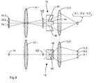
- FIG. 8 is generated by a first imaging optics 12.1 an intermediate image 10 'of the structure 10. Close to this intermediate image 10 ', the optical element 18 is arranged.
- the optical element 18 is designed such that each section 10.1, 10.2, 10.3 of the intermediate image 10 'comes to coincide with a region of the optical element 18.
- the example shown remains the area of the middle section 10.2. of the intermediate image 10 ', so that the imaging rays of this subsection 10.2 can pass unaffected by the optical element 18.
- the optical gratings 42 and 44 Like the axial view of the optical element 18 in FIG.
- the optical gratings 42 and 44 are each slanted at 45 °, with the optical grating 42 and the optical grating 42 Grids 44 are placed against each other at an angle of 90 °.
- the figures 16.1 and 16.3 are deflected laterally in different directions, so that these figures 16.1 and 16.3 on both sides next to the Figure 16. 2 of the central portion of the structure 10 are imaged on the image sensor 14, as shown in the schematic diagram of FIG. 3 equivalent.
- FIG. 9 In the upper illustration a) a side view and in the lower illustration b) a top view of the device are shown. Except for the formation of the optical element 18 corresponds to the execution of FIG. 9 the previously described embodiment of FIG. 8 ,
- the optical element 18 is in the embodiment of FIG. 9 formed as a dual prism, which is disposed immediately adjacent to the intermediate image 10 '.
- the middle region 46 of the optical element 18 assigned to the middle subsection of the intermediate image 10 ' is formed with plane-parallel surfaces, so that the imaging rays of the central subsection 10.2 can pass uninfluenced.
- the two adjacent outer sections 10.1 and 10.2 of the intermediate image 10 ' are each a prism part 48 and 50 associated with the prism surfaces of these prisms 48 and 50 both against the axis of the longitudinal extent (X-axis) and against the axis of the transverse extent (Y -Axis) of the intermediate image 10 'are inclined.
- the two partial prisms 48 and 50 are mutually inclined differently.
- the partial prisms 48 and 50 deflect the imaging beams of the respectively assigned subsections 10.1 and 10.2 of the intermediate image 10 'on the image recorder 14 into separate imaging regions, which are in the Y-axis against the image 16. 2 of the central portion 10.2 are offset to the right or to the left, as shown in the schematic representation of FIG. 3 equivalent.
- the division and deflection of the imaging beams for the images 16.1, 16.2, 16.3 of the subsections 10.1, 10.2, 10.3 of the structure 10 can also be realized by correspondingly designed other optical elements 18, eg with mirror surfaces. It is important in each case that the optical element 18 is arranged in the vicinity of the intermediate image 10 ', so that the sections 10.1, 10.2, 10.3 of the intermediate image 10' are imaged separately on the image recorder 14. For this it is also possible, for example, the optical element 18 through To realize optical fibers, which lead the corresponding areas of the subsections of the intermediate image to different subregions of the image sensor 14.
- the prisms 48, 50 are designed in such a way that they provide an offset of 22.5 °, then, in combination with an optics which has a monitoring angle of 45 °, the result is a total viewing angle of 90 °.
- a 45 ° optic is much easier, brighter and less expensive to produce than a 90 ° optic because of the lower required number of lenses with less stringent tolerance requirements.
- a focal length which is higher by a factor of 2 can be selected, which is especially important if the pixels of the image sensor 14 are particularly large and their number is small.
- the receiving optics 12.1, 12.1 ' preferably directly adjoin each other and their optical axes are each approximately in the center of their respective associated segment on the imager 14. These associated segments, ie the pixels on each of which a portion of the structure 10 is imaged, can be taught in the assembly to ensure a nearly identical reception level. This facilitates the adjustment and allows the use of simpler optics.
- the prisms 48, 50 can be integrated into the lenses 12.1, 12.1 'or in a cover glass of the Jardinauf choirs14 by appropriate injection molding structures are provided. They preferably directly adjoin one another in the plane perpendicular to the plane of the paper and are located in front of the receiving optics.
- the prisms 48, 50 may be designed as a stepped prism with sawtooth to achieve a smaller material thickness.
- optical elements 18 can be used instead of a prism, such as mirrors, gratings or diffractive optical elements in transmission or reflection.
Abstract
Description
Die Erfindung betrifft ein Verfahren zur optischen Erfassung einer Struktur gemäß dem Oberbegriff des Patentanspruchs 1 sowie eine Vorrichtung zur optischen Erfassung einer Struktur gemäß dem Oberbegriff des Patentanspruchs 8.The invention relates to a method for optical detection of a structure according to the preamble of patent claim 1 and to a device for optically detecting a structure according to the preamble of patent claim 8.
Zur optischen Erfassung von Strukturen, z.B. zur Überwachung von Gegenständen oder Raumzonen, werden Kamerasysteme verwendet, die die zu erfassende Struktur auf einem Bildaufnehmer abbilden. Die üblicherweise eingesetzten Bildaufnehmer haben ein rechteckiges oder quadratisches Format, mit welchem die Abbildung der Struktur in einer Pixel-Matrix erfasst wird. Das Seitenverhältnis des flächigen Bildaufnehmers liegt dabei zwischen 1:1 und 1:2. Diese Bildaufnehmer sind insbesondere als CCD-Sensoren kostengünstig. Diese Bildaufnehmer haben jedoch nur eine begrenzte Punktauflösung und einen begrenzten Dynamikbereich. CMOS-Sensoren können mit einer besseren Dynamik hergestellt werden, sind jedoch kostenaufwändiger und weisen ein ungünstigeres Signal-Rausch-Verhältnis auf.For optical detection of structures, e.g. For surveillance of objects or room zones, camera systems are used, which map the structure to be detected on an image sensor. The commonly used image sensors have a rectangular or square format, with which the image of the structure is detected in a pixel matrix. The aspect ratio of the flat image recorder is between 1: 1 and 1: 2. These image sensors are cost-effective in particular as CCD sensors. However, these imagers have only limited dot resolution and limited dynamic range. CMOS sensors can be made with better dynamics, but are more expensive and have a less favorable signal-to-noise ratio.
Sollen Strukturen erfasst werden, deren eine Dimension langgestreckt ist in Bezug auf ihre zweite Dimension, so ist es oft erforderlich, eine stark verkleinernde Abbildung zu verwenden, damit die gesamt langgestreckte Struktur auf dem Bildaufnehmer abgebildet werden kann. Dadurch wird die Bildauflösung zwangsläufig gering. Soll eine Überwachung langgestreckter Strukturen mit hoher Auflösung durchgeführt werden, sind teuere Spezialsensoren als Bildaufnehmer erforderlich.If structures are to be detected whose one dimension is elongated with respect to their second dimension, it is often necessary to use a strongly decreasing image so that the overall elongated structure can be imaged on the image sensor. As a result, the image resolution inevitably low. If monitoring of elongated structures with high resolution is required, expensive special sensors are required as image sensors.
Es ist bekannt, entfernungsauflösende Bildaufnehmer einzusetzen, die in jedem Pixel mittels Photonmischdetektion einen Entfernungswert auf Basis eines Lichtlaufzeitverfahrens bestimmen. Die oben genannten Nachteile gelten für diese Art Matrixempfänger entsprechend. Besonders gravierend werden dies Nachteile, wenn die Anwendung einen Öffnungswinkel von 90° und mehr fordert, weil dann aufwändige Weitwinkelobjektive eingesetzt werden müssen, um überhaupt ein vollständiges Bild zu erhalten, und dennoch die schlechte Ausnutzung des matrixförmigen Bildsensors bei langgestreckten Strukturen und die durch das Seitenverhältnis bedingte relativ geringe Auflösung nicht vermieden werden.It is known to use distance-resolving image sensors which determine a distance value based on a light transit time method in each pixel by means of photon mixing detection. The above-mentioned disadvantages apply to this type of matrix receiver corresponding. These disadvantages become particularly serious when the application requires an opening angle of 90 ° and more, because complex wide-angle lenses have to be used in order to obtain a complete image, and yet the poor utilization of the matrix-type image sensor in the case of elongated structures and because of the aspect ratio conditional relatively low resolution can not be avoided.
Bei der Überwachung von Gegenständen oder Raumzonen in der Sicherheitstechnik wird häufig ein zweikanaliger Aufbau verwendet, um interne Fehlereinflüsse zu minimieren und die Zuverlässigkeit der Überwachung zu verbessern. Wird auch der Bildaufnehmer zweifach ausgeführt, so führt dies zu einem erheblichen Kostenaufwand. Es wird daher häufig der Sensorteil nur einfach ausgeführt und ein interner Test des Sensorteils durchgeführt, der wiederum die Ansprechzeit des Sensors erhöht.When monitoring objects or room zones in safety engineering, a dual-channel design is often used to minimize internal error and improve the reliability of the monitoring. If the image sensor is also executed twice, this leads to a considerable expense. Therefore, frequently the sensor part is simply executed and an internal test of the sensor part is carried out, which in turn increases the response time of the sensor.
Der Erfindung liegt die Aufgabe zu Grunde, die optische Erfassung von Strukturen kostengünstiger und zuverlässiger auszubilden.The invention is based on the object to form the optical detection of structures more cost effective and reliable.
Diese Aufgabe wird erfindungsgemäß gelöst durch ein Verfahren mit den Merkmalen des Patentanspruchs 1 bzw. durch eine Vorrichtung mit den Merkmalen des Patentanspruchs 8.This object is achieved by a method having the features of patent claim 1 and by a device having the features of claim 8.
Vorteilhafte Ausführungen der Erfindung sind in den jeweils rückbezogenen Unteransprüchen angegeben.Advantageous embodiments of the invention are specified in the respective dependent subclaims.
Der Erfindung liegt der Gedanke zu Grunde, dass bei der Erfassung einer Struktur mit einem quadratischen oder rechteckigen Bildaufnehmer in den meisten Fällen und insbesondere bei länglichen Strukturen nur ein geringer Teil der Sensorfläche des Bildaufnehmers für die Abbildung der Struktur ausgenutzt wird, während ein wesentlicher Teil der Sensorfläche ungenutzt bleibt. Daher wird erfindungsgemäß die Matrixfläche eines insbesondere quadratischen oder rechteckigen Bildaufnehmers für die Erfassung einer Struktur dadurch ausgenutzt, dass in den Abbildungsstrahlengang des Kamerasystems ein optisches Element eingefügt wird, welches die Struktur in wenigstens zwei von einander getrennten und gegeneinander versetzten Bereichen des Bildaufnehmers abbildet.The invention is based on the idea that when detecting a structure with a square or rectangular image sensor, in most cases, and in particular in elongated structures, only a small part of the sensor surface of the image sensor is utilized for imaging the structure, while a substantial part of the structure is used Sensor surface remains unused. Therefore, according to the invention, the matrix surface of a particularly square or rectangular image sensor for the detection of a structure is exploited by inserting into the imaging beam path of the camera system an optical element which images the structure into at least two regions of the image recorder which are separated from each other and offset from one another.
Handelt es sich bei der zu erfassenden Struktur um eine langgestreckte Struktur, deren Längserstreckung in einer Dimension, als X-Achse bezeichnet, groß ist gegen deren Abmessung in der hierzu senkrechten Dimension, als Y-Achse bezeichnet, so erzeugt das optische Element vorzugsweise eine Abbildung der Struktur in wenigstens zwei Bereichen, die in der X-Achse verlaufen und in der zu dieser senkrechten Y-Achse gegeneinander versetzt sind. Dadurch wird es möglich, einen größeren Teil der Sensorfläche oder gegebenenfalls auch die gesamte Sensorfläche eines quadratischen oder rechteckigen Bildaufnehmers bei der Abbildung einer langgestreckten Struktur auszunutzen. Dadurch kann der gleiche Bildaufnehmer auf die jeweilige Aufgabe optimal angepasst werden, also dieselbe Hardware vielseitiger eingesetzt werden.If the structure to be detected is an elongated structure whose longitudinal extent in one dimension, denoted as X-axis, is large against its dimension in the dimension perpendicular thereto, referred to as the Y-axis, the optical element preferably produces an image the structure in at least two areas which extend in the X-axis and are offset from each other in the Y-axis perpendicular to this. This makes it possible to take advantage of a larger part of the sensor surface or optionally also the entire sensor surface of a square or rectangular image sensor in the image of an elongated structure. As a result, the same image recorder can be optimally adapted to the respective task, ie the same hardware can be used more versatile.
Die erfindungsgemäße Abbildung der Struktur in zwei oder mehr voneinander getrennten gegeneinander versetzten Bereichen kann in unterschiedlicher Weise vorteilhaft verwendet werden.The inventive illustration of the structure in two or more mutually separated staggered areas can be used advantageously in different ways.
In einer Ausführung wird jeweils die gesamte Struktur auf dem Bildaufnehmer in den zwei gegeneinander versetzten Bereichen abgebildet. Hierdurch ergibt sich zwar keine Verbesserung der Auflösung, man erhält jedoch eine redundante Abbildung. Fallen einzelne Bildpunkte (Pixel) in einer der Abbildungen aus, so können diese fehlerhaften Bildpunkte einer Abbildung durch die entsprechenden Bildpunkte der versetzten zweiten Abbildung ergänzt werden. Die mehrfache redundante Abbildung der gesamten Struktur ergibt somit eine zweikanalige Überwachung mit nur einem Bildaufnehmer, so dass die Zuverlässigkeit der zweikanaligen Überwachung in kostengünstiger Weise realisiert wird.In one embodiment, the entire structure is imaged on the image sensor in the two staggered areas. Although this does not improve the resolution, it does give a redundant image. If individual pixels (pixels) fail in one of the images, then these defective pixels of an image can be supplemented by the corresponding pixels of the offset second image. The multiple redundant mapping of the entire structure thus results in a two-channel monitoring with only one image sensor, so that the reliability of the two-channel monitoring is realized in a cost effective manner.
In einer anderen Ausführung wird ebenfalls die gesamte Struktur in einem Bereich des Bildaufnehmers abgebildet. Die wenigstens eine weitere übereinstimmende Abbildung der gesamten Struktur wird in einem getrennten Bereich so abgebildet, dass sie um einen Subpixel-Abstand gegenüber dem Rasterabstand der Bildpunkte in der Matrix des Bildaufnehmers im Vergleich zu der ersten Abbildung versetzt ist. Der Versatz der Abbildung weicht somit von einem ganzzahligen Vielfachen des Pixelabstandes des Bildaufnehmers ab. Die um diesen Subpixel-Abstand gegeneinander versetzten Abbildungen derselben Struktur können dann in der Auswertung dazu verwendet werden, die Pixelauflösung der Abbildung rechnerisch zu verbessern.In another embodiment, the entire structure is also imaged in a region of the image recorder. The at least one other matching image of the entire structure is imaged in a separate area so as to be offset by a sub-pixel distance from the pitch of the pixels in the array of the imager compared to the first image. The offset of the image thus deviates from an integer multiple of the pixel spacing of the image recorder. The images of the same structure staggered by this subpixel spacing can then be used in the evaluation to mathematically improve the pixel resolution of the image.
In einer weiteren Ausführung kann die Ausnutzung der gesamten Sensorfläche dazu verwendet werden, die Auflösung der Abbildung einer langgestreckten Struktur zu verbessern. Hierzu wird die Abbildung der länglichen Struktur in deren Längserstreckung (X-Achse) in Einzelabschnitte unterteilt, die in der Y-Achse gegeneinander versetzt abgebildet werden. Damit kann eine langgestreckte Struktur ohne Verkleinerung oder mit geringerer Verkleinerung auf einem Bildaufnehmer abgebildet werden, dessen Längserstreckung in der X-Achse geringer ist, als die Abbildung der gesamten Struktur, ohne dass dadurch die Bildauflösung verringert wird.In a further embodiment, the utilization of the entire sensor surface can be used to improve the resolution of the image of an elongate structure. For this purpose, the image of the elongated structure in its longitudinal extent (X-axis) is divided into individual sections, which are shown offset from one another in the Y-axis. Thus, an elongated structure can be imaged without reduction or with a smaller reduction on an image sensor, the longitudinal extent in the X-axis is less than the image of the entire structure, without thereby reducing the image resolution.
Schließlich kann auch der Dynamikbereich des Bildaufnehmers erweitert werden. Hierzu wird wiederum die gesamte Struktur in einem Flächenbereich des Bildaufnehmers abgebildet und dieselbe Struktur wird jeweils auch in wenigstens einem getrennten und versetzten Bereich abgebildet. Die Lichtintensität der Belichtung des Bildaufnehmers in den gegeneinander versetzten Bereichen wird jedoch optisch unterschiedlich stark abgeschwächt. Damit kann ein großer Bereich der ursprünglichen Beleuchtungsintensität der Struktur in den verschiedenen gegeneinander versetzten Bereich stufenweise abgeschwächt werden, so dass jeweils in wenigstens einem dieser Bereiche die auf den Bildaufnehmer auftreffende Beleuchtungsintensität in den optimalen Dynamikbereich des Bildaufnehmers fällt. Wird beispielsweise in der Abbildung der Struktur mit der geringsten Intensitätsabschwächung der Bildaufnehmer an besonders hellen Stellen der Struktur übersteuert, so können ein oder mehrere weitere versetzte Bereiche mit stärkerer Abschwächung dazu ausgenutzt werden, diese in dem ersten Bereich übersteuerten Stellen der Struktur zu detektieren und zu ergänzen.Finally, the dynamic range of the image sensor can be extended. For this purpose, in turn, the entire structure is imaged in a surface area of the image recorder and the same structure is in each case also imaged in at least one separate and offset area. However, the light intensity of the exposure of the image sensor in the staggered areas is optically attenuated to different degrees. Thus, a large portion of the original illumination intensity of the structure in the different staggered areas can be gradually attenuated, so that in each case in at least one of these areas, the incident on the imager illumination intensity falls within the optimal dynamic range of the image sensor. If, for example, in the image of the structure with the lowest intensity attenuation, the image recorder is overridden at especially bright points in the structure, then one or more further offset regions with greater attenuation can be used to detect and supplement these points of the structure which are overdriven in the first region ,
Es ist besonders bevorzugt, die erfindungsgemäße Erfassung einer Struktur zur Absicherung einer Gefahrenquelle in einem Raumbereich einzusetzen, bei dem die Struktur auf Veränderungen überwacht wird, um unzulässige Objekteingriffe in den Raumbereich zu erkennen und gegebenenfalls eine Gefahrenquelle abzusichern. In einer derartigen sicherheitstechnischen Anwendung kommen nicht nur die Vorteile der verbesserten Ausnutzung des Bildaufnehmers zur Geltung, sondern es kann bei Bedarf der Anwendung zusätzlich durch Mehrfachabbildung der ganzen Struktur oder jeweils mehrfache Abbildung von Abschnitten der Struktur auch die Anforderung der redundanten Auswertung ohne zusätzliche Hardware erfüllt werden.It is particularly preferred to use the detection according to the invention of a structure for securing a source of danger in a spatial area in which the structure is monitored for changes in order to detect impermissible object interventions in the spatial area and, if necessary, to secure a source of danger. In such a safety-related application, not only the advantages of the improved utilization of the image sensor come into play, but it can also meet the requirement of redundant evaluation without additional hardware if required by the application in addition by multiple imaging of the whole structure or each multiple mapping of sections of the structure ,
Im Folgenden wird die Erfindung anhand von in der Zeichnung dargestellten Ausführungsbeispielen näher erläutert. Es zeigen
- Fig. 1
- schematisch eine erste Ausführung der Erfindung;
- Fig. 2
- schematisch eine zweite Ausführung der Erfindung;
- Fig. 3
- schematisch eine dritte Ausführung der Erfindung;
- Fig. 4
- schematisch eine vierte Ausführung der Erfindung;
- Fig. 5
- schematisch eine fünfte Ausführung der Erfindung;
- Fig. 6
- schematisch eine sechste Ausführung der Erfindung;
- Fig. 7
- schematisch eine siebte Ausführung der Erfindung;
- Fig. 8
- ein erstes Beispiel für die Ausgestaltung des optischen Elementes in der Ausführung der
Figur 3 ; - Fig. 9
- ein zweites Beispiel für die Ausbildung des optischen Elementes in der Ausführung der
Figur 3 in Seitenansicht a und in Draufsicht b; - Fig. 10
- ein drittes Beispiel für die Ausbildung des optischen Elementes in der Ausführung der
Figur 3 in Draufsicht mit einer zugehörigen Ansicht aus der Ebene des Bildaufnehmers; - Fig. 11
- schematisch die optische Erfassung einer Struktur nach dem Stand der Technik; und
- Fig. 12
- schematisch die Verwendung der optischen Erfassung zur Überwachung eines Sichtfeldes.
- Fig. 1
- schematically a first embodiment of the invention;
- Fig. 2
- schematically a second embodiment of the invention;
- Fig. 3
- schematically a third embodiment of the invention;
- Fig. 4
- schematically a fourth embodiment of the invention;
- Fig. 5
- schematically a fifth embodiment of the invention;
- Fig. 6
- schematically a sixth embodiment of the invention;
- Fig. 7
- schematically a seventh embodiment of the invention;
- Fig. 8
- a first example of the configuration of the optical element in the embodiment of
FIG. 3 ; - Fig. 9
- a second example of the formation of the optical element in the embodiment of
FIG. 3 in side view a and in plan view b; - Fig. 10
- a third example of the formation of the optical element in the embodiment of
FIG. 3 in plan view with an associated view from the plane of the image sensor; - Fig. 11
- schematically the optical detection of a structure according to the prior art; and
- Fig. 12
- schematically the use of the optical detection for monitoring a field of view.
In
Die Struktur 10 ist schematisch als Pfeil dargestellt, kann jedoch irgend eine Struktur sein, insbesondere eine langgestreckte Struktur, deren Ausdehnung in einer Längsrichtung (X-Achse) größer ist als ihre Bereite in der dazu senkrechten Y-Achse. Die Struktur 10 wird mit einem Kamerasystem erfasst, welches eine Abbildungsoptik 12 aufweist, die die Struktur 10 auf einen Bildaufnehmer 14 abbildet. Der Bildaufnehmer 14 ist beispielsweise ein CCD-Sensor oder ein CMOS-Sensor mit einer quadratischen oder rechteckigen Matrix von Bildpunkten (Pixel). Die Struktur 10 wird auf dem Bildaufnehmer 14 als Abbildung 16 abgebildet, die der Struktur 10 entspricht. Im Allgemeinen wird die Abbildung 16 nur einen Teilbereich der Sensorfläche des Bildaufnehmers 14 einnehmen, so dass nur dieser Teilbereich des Bildaufnehmers 14 ausgenützt wird. Insbesondere wenn die Struktur 10 eine, z.B. in der X-Achse langgestreckte Struktur ist, nutzt die Abbildung 16 nur einen in der X-Achse verlaufenden streifenförmigen Bereich des Bildaufnehmers 14 aus. Die Abbildungsoptik 12 kann gegebenenfalls so vergrößern oder verkleinern, dass die Abbildung 16 in ihrer Längserstreckung in der X-Achse die Abmessungen des Bildaufnehmers 14 in dieser X-Achse optimal ausnutzt. Die Bereiche des Bildaufnehmers 14 beiderseits der Abbildung 16 bleiben jedoch ungenutzt.The
Die Kamera 26 kann auch eine entfernungsauflösende Kamera sein, beispielsweise durch einen nicht dargestellten Lichtsender, der Lichtpulse oder moduliertes Licht aussendet, wobei die Lichtlaufzeit beziehungsweise die Phasenverschiebung zur Bestimmung von Entfernungen ermittelt wird. Alternativ kann aktive oder passive Triangulation zur Bestimmung von Entfernungswerten eingesetzt werden. Durch Ermittlung von Entfernungen kann mit Überwachung einer eindimensionalen Struktur eine Ebene zweidimensional erfasst werden. Durch Übereinanderschichten mehrerer solcher Ebenen, also einen Mehrebenensensor, ist eine leicht auszuwertende Approximation an eine dreidimensionale Raumüberwachung ermöglicht.The
Die Überwachung des Sichtfeldes 24 erfolgt in einer besonders bevorzugten sicherheitstechnischen Anwendung zur Überwachung einer nicht dargestellten Gefahrenquelle. Dabei kann es sich um eine Presse, ein Feuer, eine Schneidkante oder jede denkbare Quelle einer Verletzungsgefahr insbesondere für Bedienpersonal handeln. Erkennt eine an die Kamera 26 angeschlossene oder in diese integrierte Auswertung einen unzulässigen, also unerwarteten Objekteingriff, etwa durch Vergleich mit einer Referenzszene oder -sequenz im Sichtbereich 24 erlaubter Objekte, so schaltet sie einen Ausgang, der einen Alarm auslöst oder unmittelbar einen Abschalt- oder Absicherungsbefehl an die Gefahrenquelle erzeugt, so dass diese abgeschaltet oder sonst in einen sicheren Zustand gebracht wird.The monitoring of the field of
In den
In dem Ausführungsbeispiel der
In dem Ausführungsbeispiel der
Sind die Abbildungen 16.1, 16.2 und 16.3 in den voneinander getrennten Bereichen um einen ganzzahligen Pixel-Abstand des Bildaufnehmers 14 voneinander getrennt, so ergeben sich in diesen voneinander getrennten Bereichen jeweils identische Abbildungen 16.1, 16.2 und 16.3 der Struktur 10, wie dies für die Verwendung als redundante Abbildungen zweckmäßig ist. In einer abgewandelten Ausführung kann die Ablenkung der Abbildungsstrahlen so gewählt sein, dass die Abbildungen 16.1, 16.2 und 16.3 gegeneinander, im dargestellten Beispiel in der Y-Achse, um einen Abstand versetzt sind, der von einem ganzzahligen Vielfachen des Pixel-Abstandes des Bildaufnehmers 14 abweicht. In den voneinander getrennten Bereichen werden daher Abbildungen 16.1, 16.2 und 16.3 erfasst, die in Bezug auf die Matrix des Bildaufnehmers 14 um Subpixel-Abstände gegeneinander versetzt sind. Solche um Subpixel-Abstände gegeneinander versetzte Abbildungen 16.1, 16.2 und 16.3 können dazu ausgenützt werden, die Pixel-Auflösung des Bildaufnehmers 14 in der nachgeschalteten Bildauswertung rechnerisch zu verbessern.If the figures 16.1, 16.2 and 16.3 are separated from one another by an integer pixel spacing of the
Eine weitere Anwendung der Erfindung ist in
Die Aufspaltung der Abbildung der Struktur des Retroreflektors 22 in zwei getrennte Abbildungen 16.1 und 16.2 ermöglicht eine zweikanalige Überwachung des Sichtfeldes vor dem Retroreflektor 22 mit nur einem Bildaufnehmer 14. Die nachgeschaltete Auswertung der zwei getrennten Abbildungen 16.1 und 16.2 ergibt eine redundante Überwachung, die eine erhöhte Zuverlässigkeit gegen interne Störungen gewährleistet.The splitting of the image of the structure of the
Eine weitere Ausbildung ist in
Die verschiedenen Ausbildungen des optischen Elementes 18 als doppelreflektierende Umlenkplatte 34 in
Um eine langgestreckte Struktur 10 in einzelne Abschnitte 10.1, 10.2, 10.3 unterteilt in getrennten Bildbereichen als Teilabbildungen 16.1, 16.2, 16.3 abzubilden, wie dies schematisch in
In dem Ausführungsbeispiel der
In
Das optische Element 18 ist in der Ausführung der
Es ist für den Fachmann erkennbar, dass die Aufteilung und Umlenkung der Abbildungsstrahlen für die Abbildungen 16.1, 16.2, 16.3 der Teilabschnitte 10.1, 10.2, 10.3 der Struktur 10 auch durch entsprechend gestaltete andere optische Elemente 18, z.B. mit Spiegelflächen realisiert werden können. Wichtig ist dabei jeweils, dass das optische Element 18 in der Nähe des Zwischenbildes 10' angeordnet wird, damit die Abschnitte 10.1, 10.2, 10.3 des Zwischenbildes 10' getrennt auf dem Bildaufnehmer 14 abgebildet werden. Hierfür ist es z.B. auch möglich, das optische Element 18 durch Lichtleitfasern zu realisieren, die die entsprechenden Bereiche der Teilabschnitte des Zwischenbildes zu verschiedenen Teilbereichen des Bildaufnehmers 14 führen.It is obvious to the person skilled in the art that the division and deflection of the imaging beams for the images 16.1, 16.2, 16.3 of the subsections 10.1, 10.2, 10.3 of the
In einem weiteren Ausführungsbeispiel gemäß
Mit einer derartigen in der Draufsicht dargestellten Prismenanordnung 48, 50 erreicht man eine Verschiebung zweier Teile der Struktur 10 in einer Ebene. Im linken Teil der
Die Empfangsoptiken 12.1, 12.1' schließen bevorzugt direkt aneinander an und ihre optischen Achsen liegen jeweils ungefähr im Zentrum ihres jeweiligen zugehörigen Segments auf dem Bildaufnehmer 14. Diese zugehörigen Segmente, also die Pixel, auf denen jeweils ein Abschnitt der Struktur 10 abgebildet wird, können nach der Montage eingelernt werden, um eine nahezu gleiche Empfangsebene zu gewährleisten. Das erleichtert die Justierung und erlaubt den Einsatz einfacherer Optiken.The receiving optics 12.1, 12.1 'preferably directly adjoin each other and their optical axes are each approximately in the center of their respective associated segment on the
Die Prismen 48, 50 können in die Linsen 12.1, 12.1' oder in ein Deckglas des Bildaufnehmers14 integriert werden, indem entsprechende Spritzgussstrukturen vorgesehen werden. Sie schließen bevorzugt in der Ebene senkrecht zur Papierebene unmittelbar aneinander an und sitzen vor der Empfangsoptik. Die Prismen 48, 50 können als Stufenprisma mit Sägezahn ausgeführt sein, um eine geringere Materialdicke zu erreichen.The
Auch in der Ausführungsform ohne Zwischenbild 10' können anstelle eines Prismas andere optische Elemente 18 eingesetzt werden, etwa Spiegel, Gitter oder diffraktive optische Elemente in Transmission oder Reflexion.Also in the embodiment without intermediate image 10 ', other
- 1010
- Strukturstructure
- 1212
- Abbildungsoptikimaging optics
- 1414
- Bildaufnehmerimager
- 1616
- AbbildungIllustration
- 1818
- optisches Elementoptical element
- 2020
- Abschwächerattenuator
- 2222
- Retroreflektorretroreflector
- 2424
- Sichtfeldfield of view
- 2626
- Kameracamera
- 2828
- Wändewalls
- 3030
- Umlenkprismadeflecting prism
- 3232
- Lichtquellelight source
- 3434
- Umlenkplattebaffle
- 3636
- Umlenkprismadeflecting prism
- 3838
- Spiegelflächenmirror surfaces
- 4040
- Doppelprismadouble prism
- 4242
- optisches Gitteroptical grating
- 4444
- optisches Gitteroptical grating
- 4646
- mittlerer Bereichmiddle area
- 48, 5048, 50
- Teilprismensubprisms
Claims (15)
dadurch gekennzeichnet, dass ein in dem Abbildungstrahlengang angeordnetes optisches Element die Struktur in wenigstens zwei voneinander getrennten und gegeneinander versetzten Bereichen des Bildaufnehmers abbildet.Method for optically detecting a structure in which the structure is imaged on an image sensor,
characterized in that an optical element arranged in the imaging beam path images the structure in at least two separate and mutually offset regions of the image sensor.
wobei die wenigstens zwei Bereiche parallel zueinander und quer zueinander versetzt angeordnet sind.Method according to claim 1,
wherein the at least two regions are arranged offset parallel to one another and transversely to one another.
wobei in den wenigstens zwei voneinander getrennten Bereichen jeweils die gesamte Struktur abgebildet wird.Method according to claim 1 or 2,
wherein in each case the entire structure is imaged in the at least two separate regions.
wobei die Struktur in Abschnitte unterteilt wird und diese Abschnitte jeweils wenigstens einmal in voneinander getrennten Bereichen abgebildet werden.Method according to claim 1 or 2,
wherein the structure is divided into sections and these sections are each at least once imaged in separate areas.
wobei die Abbildungen in den voneinander getrennten Bereichen als redundante Abbildungen zur Erhöhung der Zuverlässigkeit der Erfassung verarbeitet werden.Method according to one of the preceding claims,
wherein the images in the separate regions are processed as redundant images to increase the reliability of the detection.
wobei in den gegeneinander versetzten Bereichen die Abbildung der Struktur gegenüber dem Bildaufnehmer um einen unterschiedlichen Subpixel-Abstand versetzt ist und/oder wobei die Lichtintensität der Abbildungsstrahlen für wenigstens zwei Abbildungen in gegeneinander versetzten Bereichen unterschiedlich stark geschwächt wird.Method according to one of the preceding claims,
wherein in the mutually offset areas, the image of the structure with respect to the image sensor is offset by a different subpixel spacing and / or wherein the light intensity of the imaging beams is weakened to different degrees for at least two images in mutually offset areas.
gekennzeichnet durch ein optisches Element (18), das in dem Abbildungsstrahlengang angeordnet ist und die Abbildungsstrahlen der Struktur (10) in wenigstens zwei voneinander getrennte und gegeneinander versetzte Bereiche des Bildaufnehmers (14) ablenkt.Apparatus for optically detecting a structure (10) with a camera system having an imager (14) on which the structure (10) is imaged,
characterized by an optical element (18) disposed in the imaging beam path and deflecting the imaging beams of the structure (10) into at least two separate and staggered regions of the imaging member (14).
dadurch gekennzeichnet, dass bei der Abbildung einer langgestreckten Struktur (10) die gegeneinander versetzten Bereiche des Bildaufnehmers (14) zur Längserstreckung der Struktur (X-Achse) parallel verlaufen und quer zur Längserstreckung der Struktur (Y-Achse) gegeneinander versetzt sind.Device according to claim 8,
characterized in that in the image of an elongated structure (10) the mutually offset portions of the image sensor (14) extend parallel to the longitudinal extent of the structure (X-axis) and offset from each other transversely to the longitudinal extent of the structure (Y-axis).
dadurch gekennzeichnet, dass das optische Element (18) in den wenigstens zwei Bereichen jeweils eine Abbildung (16.1, 16.2, 16.3) der gesamten Struktur (10) erzeugt.Device according to claim 8 or 9,
characterized in that the optical element (18) in each of the at least two regions generates an image (16.1, 16.2, 16.3) of the entire structure (10).
dadurch gekennzeichnet, dass das optische Element (18) in den wenigstens zwei Bereichen jeweils eine Abbildung (16.1, 16.2, 16.3) der gesamten Struktur (10) erzeugt, wobei diese Abbildungen (16.1, 16.2, 16.3) um einen Abstand gegeneinander versetzt sind, der von einem ganzzahligen Vielfachen des Pixel-Abstandes des Bildaufnehmers (14) abweicht.Device according to one of claims 8 to 10,
characterized in that the optical element (18) in each of the at least two regions generates an image (16.1, 16.2, 16.3) of the entire structure (10), these images (16.1, 16.2, 16.3) being offset from one another by a distance, which differs from an integer multiple of the pixel pitch of the imager (14).
dadurch gekennzeichnet, dass in den den gegeneinander versetzten Bereichen zugeordneten Strahlengängen ein optischer Abschwächer (20) angeordnet ist, der die Intensität der diesen Bereichen jeweils zugeordneten Abbildungsstrahlen unterschiedlich abschwächt.Device according to one of claims 8 to 10,
characterized in that an optical attenuator (20) is arranged in the beam paths assigned to the mutually offset regions, which attenuates the intensity of the imaging beams associated with these areas differently.
dadurch gekennzeichnet, dass das optische Element (18) die Struktur (10) in Längsabschnitte (10.1, 10.2, 10.3) unterteilt in den gegeneinander versetzten Bereichen abbildet.Device according to claim 8 or 9,
characterized in that the optical element (18) the structure (10) in longitudinal sections (10.1, 10.2, 10.3) divided in the mutually offset areas images.
dadurch gekennzeichnet, dass das optische Element (18) wenigstens ein optisches Gitter, ein Prisma, einen Spiegel oder ein diffraktives optisches Element aufweist, wobei das optische Element (18) insbesondere in eine Abbildungsoptik (12) des Bildaufnehmers (14) integriert ist.Device according to one of claims 8 to 13,
characterized in that the optical element (18) comprises at least one optical grating, a prism, a mirror or a diffractive optical element, wherein the optical element (18) in particular in an imaging optics (12) of the image sensor (14) is integrated.
wobei der Sensor eine Vorrichtung nach einem der Ansprüche 8 bis 14 aufweist, um die Struktur optisch zu erfassen.Optoelectronic sensor, in particular distance-resolving sensor, for securing a source of danger in a spatial area in which an evaluation unit is adapted to monitor a structure for changes, to detect impermissible object interference in the spatial area, and having a warning or shutdown device, which with the evaluation unit is connected and which can secure the source of danger,
wherein the sensor comprises a device according to any one of claims 8 to 14 for optically detecting the structure.
Applications Claiming Priority (1)
| Application Number | Priority Date | Filing Date | Title |
|---|---|---|---|
| DE102006058057A DE102006058057B3 (en) | 2006-12-07 | 2006-12-07 | Method and device for optically detecting a structure |
Publications (1)
| Publication Number | Publication Date |
|---|---|
| EP1931133A1 true EP1931133A1 (en) | 2008-06-11 |
Family
ID=38965055
Family Applications (1)
| Application Number | Title | Priority Date | Filing Date |
|---|---|---|---|
| EP07119614A Withdrawn EP1931133A1 (en) | 2006-12-07 | 2007-10-30 | Method and device for optical acquisition of a structure |
Country Status (2)
| Country | Link |
|---|---|
| EP (1) | EP1931133A1 (en) |
| DE (1) | DE102006058057B3 (en) |
Cited By (7)
| Publication number | Priority date | Publication date | Assignee | Title |
|---|---|---|---|---|
| EP2749941A1 (en) * | 2011-08-24 | 2014-07-02 | Olympus Medical Systems Corp. | Image capture device and iamge capture device system |
| DE202014101927U1 (en) | 2014-04-24 | 2015-07-27 | Sick Ag | Camera for detecting a moving stream of objects |
| DE202014102452U1 (en) | 2014-05-26 | 2015-08-27 | Sick Ag | Camera for recording image data |
| EP2937810A1 (en) | 2014-04-24 | 2015-10-28 | Sick Ag | Camera and method for detecting a moving flow of objects |
| EP2950519A1 (en) | 2014-05-26 | 2015-12-02 | Sick Ag | Camera and method for capturing image data |
| DE102022114792B3 (en) | 2022-06-13 | 2023-11-02 | Sick Ag | LIGHT TRANSMITTER ARRANGEMENT AND OPTOELECTRONIC SENSOR ARRANGEMENT |
| DE102022005025A1 (en) | 2022-06-13 | 2023-12-14 | Sick Ag | OPTOELECTRONIC SENSOR |
Families Citing this family (1)
| Publication number | Priority date | Publication date | Assignee | Title |
|---|---|---|---|---|
| EP2199999B1 (en) | 2008-12-19 | 2012-05-02 | Pepperl + Fuchs GmbH | Method for testing an optical sensor and testable optical sensor |
Citations (10)
| Publication number | Priority date | Publication date | Assignee | Title |
|---|---|---|---|---|
| DE2822027A1 (en) * | 1977-05-20 | 1978-11-23 | Asahi Optical Co Ltd | DEVICE FOR THE FOCUS ADJUSTMENT OF THE LENS OF A SINGLE-EYE REFLECTIVE REFLECTIVE CAMERA |
| EP0083240A2 (en) | 1981-12-25 | 1983-07-06 | Kabushiki Kaisha Toshiba | Solid state image sensor with high resolution |
| JPS58113729A (en) * | 1981-12-26 | 1983-07-06 | Toshiba Corp | One-dimensional detector |
| GB2140649A (en) | 1983-04-08 | 1984-11-28 | Citizen Watch Co Ltd | Correcting for faulty photodetectors in an image pickup system |
| WO1988002971A1 (en) | 1986-10-17 | 1988-04-21 | Kenneth Gural | Solid state imaging device having means to shift the image between scans and associated circuitry to improve the scanned image |
| EP0286393A2 (en) * | 1987-04-10 | 1988-10-12 | British Aerospace Public Limited Company | Imaging system |
| US5070407A (en) | 1990-05-11 | 1991-12-03 | Wheeler Ernest E | Filter changing mechanism for a video camera |
| US5889553A (en) | 1993-11-17 | 1999-03-30 | Canon Kabushiki Kaisha | Image pickup apparatus capable of high resolution imaging |
| WO2005043893A1 (en) | 2003-11-04 | 2005-05-12 | Matsushita Electric Industrial Co., Ltd. | Imaging device |
| JP2006154506A (en) * | 2004-11-30 | 2006-06-15 | Nikon Corp | Optical element and focus detector |
Family Cites Families (2)
| Publication number | Priority date | Publication date | Assignee | Title |
|---|---|---|---|---|
| GB2284273B (en) * | 1993-11-29 | 1997-01-08 | Hadland Photonics Limited | Electronic high speed camera incorporating a beam splitter |
| DE10223923B4 (en) * | 2002-05-23 | 2004-07-22 | Robot Visual Systems Gmbh | Method and arrangement for photographing a vehicle |
-
2006
- 2006-12-07 DE DE102006058057A patent/DE102006058057B3/en not_active Expired - Fee Related
-
2007
- 2007-10-30 EP EP07119614A patent/EP1931133A1/en not_active Withdrawn
Patent Citations (11)
| Publication number | Priority date | Publication date | Assignee | Title |
|---|---|---|---|---|
| DE2822027A1 (en) * | 1977-05-20 | 1978-11-23 | Asahi Optical Co Ltd | DEVICE FOR THE FOCUS ADJUSTMENT OF THE LENS OF A SINGLE-EYE REFLECTIVE REFLECTIVE CAMERA |
| EP0083240A2 (en) | 1981-12-25 | 1983-07-06 | Kabushiki Kaisha Toshiba | Solid state image sensor with high resolution |
| JPS58113729A (en) * | 1981-12-26 | 1983-07-06 | Toshiba Corp | One-dimensional detector |
| GB2140649A (en) | 1983-04-08 | 1984-11-28 | Citizen Watch Co Ltd | Correcting for faulty photodetectors in an image pickup system |
| WO1988002971A1 (en) | 1986-10-17 | 1988-04-21 | Kenneth Gural | Solid state imaging device having means to shift the image between scans and associated circuitry to improve the scanned image |
| EP0286393A2 (en) * | 1987-04-10 | 1988-10-12 | British Aerospace Public Limited Company | Imaging system |
| US5070407A (en) | 1990-05-11 | 1991-12-03 | Wheeler Ernest E | Filter changing mechanism for a video camera |
| US5889553A (en) | 1993-11-17 | 1999-03-30 | Canon Kabushiki Kaisha | Image pickup apparatus capable of high resolution imaging |
| WO2005043893A1 (en) | 2003-11-04 | 2005-05-12 | Matsushita Electric Industrial Co., Ltd. | Imaging device |
| US20070091197A1 (en) * | 2003-11-04 | 2007-04-26 | Hiroaki Okayama | Imaging device |
| JP2006154506A (en) * | 2004-11-30 | 2006-06-15 | Nikon Corp | Optical element and focus detector |
Non-Patent Citations (1)
| Title |
|---|
| MANOJ AGGARWAL ET AL: "Split Aperture Imaging for High Dynamic Range", INTERNATIONAL JOURNAL OF COMPUTER VISION, KLUWER ACADEMIC PUBLISHERS, BO, vol. 58, no. 1, 1 June 2004 (2004-06-01), pages 7 - 17, XP019216408, ISSN: 1573-1405, DOI: 10.1023/B:VISI.0000016144.56397.1A * |
Cited By (10)
| Publication number | Priority date | Publication date | Assignee | Title |
|---|---|---|---|---|
| EP2749941A1 (en) * | 2011-08-24 | 2014-07-02 | Olympus Medical Systems Corp. | Image capture device and iamge capture device system |
| EP2749941A4 (en) * | 2011-08-24 | 2015-04-22 | Olympus Medical Systems Corp | Image capture device and iamge capture device system |
| DE202014101927U1 (en) | 2014-04-24 | 2015-07-27 | Sick Ag | Camera for detecting a moving stream of objects |
| EP2937810A1 (en) | 2014-04-24 | 2015-10-28 | Sick Ag | Camera and method for detecting a moving flow of objects |
| DE102014105759A1 (en) | 2014-04-24 | 2015-10-29 | Sick Ag | Camera and method for detecting a moving stream of objects |
| DE202014102452U1 (en) | 2014-05-26 | 2015-08-27 | Sick Ag | Camera for recording image data |
| EP2950519A1 (en) | 2014-05-26 | 2015-12-02 | Sick Ag | Camera and method for capturing image data |
| DE102022114792B3 (en) | 2022-06-13 | 2023-11-02 | Sick Ag | LIGHT TRANSMITTER ARRANGEMENT AND OPTOELECTRONIC SENSOR ARRANGEMENT |
| DE102022005025A1 (en) | 2022-06-13 | 2023-12-14 | Sick Ag | OPTOELECTRONIC SENSOR |
| EP4293395A2 (en) | 2022-06-13 | 2023-12-20 | Sick Ag | Optoelectronic sensor and light emitter assembly |
Also Published As
| Publication number | Publication date |
|---|---|
| DE102006058057B3 (en) | 2008-07-24 |
Similar Documents
| Publication | Publication Date | Title |
|---|---|---|
| EP3729137B1 (en) | Multi-pulse lidar system for multi-dimensional detection of objects | |
| EP1931133A1 (en) | Method and device for optical acquisition of a structure | |
| EP0578129B1 (en) | Imaging sensor unit | |
| EP1933167B1 (en) | Optoelectronic sensor and method for detecting and determining the distance of an object | |
| EP1947481B1 (en) | Optoelectronic sensor and method for recording objects in a monitoring area | |
| CH651408A5 (en) | OPTICAL DOCUMENT TEST DEVICE FOR DETECTING MISTAKE PRESSURES. | |
| DE102007004632A1 (en) | Rear-scattered article detecting method for opto-electronic device, involves producing signal pattern on pixel array corresponding to images of light spots, and determining information about sensing distance between device and article | |
| DE202008013217U1 (en) | Illumination for generating a contrast pattern | |
| EP1065521B1 (en) | Optoelectronic surveillance system | |
| DE102009046108A1 (en) | camera system | |
| DE102016220232A1 (en) | Optical element for a lidar system | |
| EP2280239A1 (en) | Illumination device for lighting a monitored area | |
| WO2021037556A1 (en) | Camera device for generating an image of surroundings | |
| EP0907902A1 (en) | Method of three-dimensional imaging on a large-screen projection surface using a laser projector | |
| EP0402601A2 (en) | Optoelectronic viewing assembly | |
| DE3232092C1 (en) | Day-vision/night-vision device | |
| EP1467185A1 (en) | Lens assembly for an optical encoder | |
| DE19718390A1 (en) | Opto-electronic sensor | |
| DE102018204708A1 (en) | Macroscopic lidar device | |
| EP2110699A2 (en) | Method and device for lighting an object scene | |
| DE102017101791B4 (en) | Optoelectronic sensor device for a motor vehicle and motor vehicle | |
| EP1065522B1 (en) | Optoelectronic surveillance system | |
| DE102017210683B4 (en) | Optical arrangement of a receiver optics of a scanning lidar system, lidar system and working device | |
| WO2017005653A1 (en) | Detector unit for an optical sensor device | |
| EP3496398B1 (en) | Secure stereo camera and method for testing the functionality of the image sensors |
Legal Events
| Date | Code | Title | Description |
|---|---|---|---|
| PUAI | Public reference made under article 153(3) epc to a published international application that has entered the european phase |
Free format text: ORIGINAL CODE: 0009012 |
|
| AK | Designated contracting states |
Kind code of ref document: A1 Designated state(s): AT BE BG CH CY CZ DE DK EE ES FI FR GB GR HU IE IS IT LI LT LU LV MC MT NL PL PT RO SE SI SK TR |
|
| AX | Request for extension of the european patent |
Extension state: AL BA HR MK RS |
|
| 17P | Request for examination filed |
Effective date: 20080409 |
|
| AKX | Designation fees paid |
Designated state(s): AT BE BG CH CY CZ DE DK EE ES FI FR GB GR HU IE IS IT LI LT LU LV MC MT NL PL PT RO SE SI SK TR |
|
| 17Q | First examination report despatched |
Effective date: 20100302 |
|
| STAA | Information on the status of an ep patent application or granted ep patent |
Free format text: STATUS: THE APPLICATION HAS BEEN WITHDRAWN |
|
| 18W | Application withdrawn |
Effective date: 20130807 |