EP1953577A2 - Package for optoelectronic device on wafer level and associated methods - Google Patents
Package for optoelectronic device on wafer level and associated methods Download PDFInfo
- Publication number
- EP1953577A2 EP1953577A2 EP08009231A EP08009231A EP1953577A2 EP 1953577 A2 EP1953577 A2 EP 1953577A2 EP 08009231 A EP08009231 A EP 08009231A EP 08009231 A EP08009231 A EP 08009231A EP 1953577 A2 EP1953577 A2 EP 1953577A2
- Authority
- EP
- European Patent Office
- Prior art keywords
- substrate
- layer
- optoelectronic device
- spacer
- mount
- Prior art date
- Legal status (The legal status is an assumption and is not a legal conclusion. Google has not performed a legal analysis and makes no representation as to the accuracy of the status listed.)
- Granted
Links
- 230000005693 optoelectronics Effects 0.000 title claims abstract description 62
- 238000000034 method Methods 0.000 title claims description 19
- 239000000758 substrate Substances 0.000 claims abstract description 213
- 230000003287 optical effect Effects 0.000 claims abstract description 135
- 125000006850 spacer group Chemical group 0.000 claims abstract description 67
- 238000007789 sealing Methods 0.000 claims abstract description 9
- 238000004519 manufacturing process Methods 0.000 claims description 4
- 235000012431 wafers Nutrition 0.000 description 47
- 239000004020 conductor Substances 0.000 description 11
- 238000000926 separation method Methods 0.000 description 7
- 229910000679 solder Inorganic materials 0.000 description 7
- 239000000835 fiber Substances 0.000 description 6
- 239000000463 material Substances 0.000 description 6
- 230000013011 mating Effects 0.000 description 5
- 238000000059 patterning Methods 0.000 description 5
- XUIMIQQOPSSXEZ-UHFFFAOYSA-N Silicon Chemical compound [Si] XUIMIQQOPSSXEZ-UHFFFAOYSA-N 0.000 description 4
- 229910052710 silicon Inorganic materials 0.000 description 4
- 239000010703 silicon Substances 0.000 description 4
- RZVAJINKPMORJF-UHFFFAOYSA-N Acetaminophen Chemical compound CC(=O)NC1=CC=C(O)C=C1 RZVAJINKPMORJF-UHFFFAOYSA-N 0.000 description 3
- 239000011248 coating agent Substances 0.000 description 3
- 238000000576 coating method Methods 0.000 description 3
- 230000008878 coupling Effects 0.000 description 3
- 238000010168 coupling process Methods 0.000 description 3
- 238000005859 coupling reaction Methods 0.000 description 3
- 239000002184 metal Substances 0.000 description 3
- 239000005297 pyrex Substances 0.000 description 3
- 239000000919 ceramic Substances 0.000 description 2
- 238000005530 etching Methods 0.000 description 2
- 238000004806 packaging method and process Methods 0.000 description 2
- QCEUXSAXTBNJGO-UHFFFAOYSA-N [Ag].[Sn] Chemical compound [Ag].[Sn] QCEUXSAXTBNJGO-UHFFFAOYSA-N 0.000 description 1
- 238000004891 communication Methods 0.000 description 1
- 238000010276 construction Methods 0.000 description 1
- 239000012799 electrically-conductive coating Substances 0.000 description 1
- 239000011521 glass Substances 0.000 description 1
- JVPLOXQKFGYFMN-UHFFFAOYSA-N gold tin Chemical compound [Sn].[Au] JVPLOXQKFGYFMN-UHFFFAOYSA-N 0.000 description 1
- 238000007373 indentation Methods 0.000 description 1
- 238000002844 melting Methods 0.000 description 1
- 230000008018 melting Effects 0.000 description 1
- 238000012986 modification Methods 0.000 description 1
- 230000004048 modification Effects 0.000 description 1
- 238000012544 monitoring process Methods 0.000 description 1
- 230000003647 oxidation Effects 0.000 description 1
- 238000007254 oxidation reaction Methods 0.000 description 1
- 238000012545 processing Methods 0.000 description 1
- 238000009877 rendering Methods 0.000 description 1
- 239000012780 transparent material Substances 0.000 description 1
Images


Classifications
-
- G—PHYSICS
- G02—OPTICS
- G02B—OPTICAL ELEMENTS, SYSTEMS OR APPARATUS
- G02B6/00—Light guides; Structural details of arrangements comprising light guides and other optical elements, e.g. couplings
- G02B6/24—Coupling light guides
- G02B6/42—Coupling light guides with opto-electronic elements
- G02B6/4201—Packages, e.g. shape, construction, internal or external details
- G02B6/4251—Sealed packages
-
- G—PHYSICS
- G02—OPTICS
- G02B—OPTICAL ELEMENTS, SYSTEMS OR APPARATUS
- G02B6/00—Light guides; Structural details of arrangements comprising light guides and other optical elements, e.g. couplings
- G02B6/24—Coupling light guides
- G02B6/42—Coupling light guides with opto-electronic elements
- G02B6/4201—Packages, e.g. shape, construction, internal or external details
- G02B6/4256—Details of housings
- G02B6/4257—Details of housings having a supporting carrier or a mounting substrate or a mounting plate
-
- H—ELECTRICITY
- H01—ELECTRIC ELEMENTS
- H01L—SEMICONDUCTOR DEVICES NOT COVERED BY CLASS H10
- H01L31/00—Semiconductor devices sensitive to infrared radiation, light, electromagnetic radiation of shorter wavelength or corpuscular radiation and specially adapted either for the conversion of the energy of such radiation into electrical energy or for the control of electrical energy by such radiation; Processes or apparatus specially adapted for the manufacture or treatment thereof or of parts thereof; Details thereof
- H01L31/02—Details
- H01L31/0203—Containers; Encapsulations, e.g. encapsulation of photodiodes
-
- H—ELECTRICITY
- H01—ELECTRIC ELEMENTS
- H01L—SEMICONDUCTOR DEVICES NOT COVERED BY CLASS H10
- H01L31/00—Semiconductor devices sensitive to infrared radiation, light, electromagnetic radiation of shorter wavelength or corpuscular radiation and specially adapted either for the conversion of the energy of such radiation into electrical energy or for the control of electrical energy by such radiation; Processes or apparatus specially adapted for the manufacture or treatment thereof or of parts thereof; Details thereof
- H01L31/02—Details
- H01L31/0232—Optical elements or arrangements associated with the device
- H01L31/02325—Optical elements or arrangements associated with the device the optical elements not being integrated nor being directly associated with the device
-
- G—PHYSICS
- G02—OPTICS
- G02B—OPTICAL ELEMENTS, SYSTEMS OR APPARATUS
- G02B6/00—Light guides; Structural details of arrangements comprising light guides and other optical elements, e.g. couplings
- G02B6/24—Coupling light guides
- G02B6/42—Coupling light guides with opto-electronic elements
- G02B6/4201—Packages, e.g. shape, construction, internal or external details
- G02B6/4204—Packages, e.g. shape, construction, internal or external details the coupling comprising intermediate optical elements, e.g. lenses, holograms
-
- G—PHYSICS
- G02—OPTICS
- G02B—OPTICAL ELEMENTS, SYSTEMS OR APPARATUS
- G02B6/00—Light guides; Structural details of arrangements comprising light guides and other optical elements, e.g. couplings
- G02B6/24—Coupling light guides
- G02B6/42—Coupling light guides with opto-electronic elements
- G02B6/4201—Packages, e.g. shape, construction, internal or external details
- G02B6/4219—Mechanical fixtures for holding or positioning the elements relative to each other in the couplings; Alignment methods for the elements, e.g. measuring or observing methods especially used therefor
- G02B6/4228—Passive alignment, i.e. without a detection of the degree of coupling or the position of the elements
- G02B6/4232—Passive alignment, i.e. without a detection of the degree of coupling or the position of the elements using the surface tension of fluid solder to align the elements, e.g. solder bump techniques
-
- G—PHYSICS
- G02—OPTICS
- G02B—OPTICAL ELEMENTS, SYSTEMS OR APPARATUS
- G02B6/00—Light guides; Structural details of arrangements comprising light guides and other optical elements, e.g. couplings
- G02B6/24—Coupling light guides
- G02B6/42—Coupling light guides with opto-electronic elements
- G02B6/4292—Coupling light guides with opto-electronic elements the light guide being disconnectable from the opto-electronic element, e.g. mutually self aligning arrangements
-
- H—ELECTRICITY
- H01—ELECTRIC ELEMENTS
- H01L—SEMICONDUCTOR DEVICES NOT COVERED BY CLASS H10
- H01L2924/00—Indexing scheme for arrangements or methods for connecting or disconnecting semiconductor or solid-state bodies as covered by H01L24/00
- H01L2924/0001—Technical content checked by a classifier
- H01L2924/0002—Not covered by any one of groups H01L24/00, H01L24/00 and H01L2224/00
Definitions
- the present invention is directed to a wafer based optical chassis and associated methods. More particularly, the present invention is directed to protecting active elements in an optical system and realizing electrical input/output without requiring separate packaging.
- Active elements such as optoelectronic chips, e.g., light sources for transmitters and detectors for receivers, are typically housed in a transistor outline (TO) can.
- TO transistor outline
- Such a TO can is typically made of metal, has a large form factor, involves an expensive serial manufacturing process and requires active alignment with external passive optical elements. This large form factor separates the active element from an external passive optic along the optical axis, resulting in the passive optic needing to handle a more divergent beam, rendering the optic bigger, thereby further increasing the size of the system.
- the TO can has electrical termination concerns, limiting the speed of the active elements.
- the present invention is therefore directed to a wafer based optical chassis and associated methods that substantially overcome one or more of the problems due to the limitations and disadvantages of the related art.
- At least one of the above and other features may be realized by providing an optical apparatus Including a mount substrate, an optoelectronic device on the mount substrate, a spacer substrate and a sealer substrate.
- the mount substrate, the spacer substrate and the sealer substrate are vertically stacked and hermetically seal the optoelectronic device.
- the apparatus also Includes external electrical contact for the optoelectronic device outside the sealing.
- the spacer substrate may be angled and have a reflective material thereon.
- the electrical contact may include a metalized trench.
- the mount substrate and the spacer substrate may be flush.
- the optical apparatus as may include a ledge formed by differing widths between the mount substrate and the spacer substrate.
- the metalized trenches may be in the ledge or the electrical contact may be on the ledge.
- the electrical contact may include a conductive via on a bottom surface of the mount substrate and a conductive structure In the via.
- the conductive structure is a solder ball.
- the electrical contact may include a conductive material on at least two non-parallel surfaces of the mount substrate.
- a passive optical element may be on a surface of the sealer substrate.
- the optical apparatus may include, above the sealer substrate, an optical block having a passive optical element on at least one surface thereof.
- the optical apparatus may Include, above the sealer substrate, an isolator stack Including first and second polarizers and a Faraday rotator sandwiched between the first and second polarizers.
- the optical apparatus may Include, above the sealer substrate, another spacer substrate. At least two of the mount substrate, the spacer substrate and the sealer substrate are of materials with approximately same coefficients of thermal expansion. One of the at least two substrates may be silicon and the other may be Pyrex.
- a terminal surface of the optical apparatus may include a mating feature for mating the optical apparatus with another structure, e.g., a ferrule.
- At least one of the above and other features may be realized by providing a method of aligning an active device and a lens, including providing the active device on a mount substrate, the active device having an active area on a side thereof, positioning an angled reflector relative to the active area in accordance with a radius of curvature of the lens, viewing the active area reflected by the angled reflector, and positioning the lens In accordance with the viewed active area.
- At least one of the above and other features may be realized by providing a method of creating a plurality of optical apparatuses, including patterning a conductive material on a mount wafer, populating the mount substrate with optoelectronic devices in accordance with the patterning, stacking and securing a spacer substrate on the mount wafer, stacking and securing a sealer substrate on the spacer substrate, wherein the stacking and securing of the spacer substrate and the sealer substrate on the mount wafer hermetically seal the optoelectronic devices, and vertically separating the mount wafer to form the plurality of optical apparatuses.
- the vertically separating including exposing a portion of the conductive material outside the hermetic seal.
- Each optical apparatus includes a mount substrate, an optoelectronic device, a spacer substrate, a sealer substrate, and exposed conductive material.
- the stacking and securing of the sealer substrate to the spacer substrate occurs before stacking and securing of the spacer substrate stacked to the mount substrate.
- FIG. 1 is an elevational perspective view of an embodiment of the optical chassis of the present invention
- FIG. 2 is a detailed elevational perspective view of the optoelectronic devices and electrical interconnections of the optical chassis of FIG. 1 ;
- FIG. 3 is an elevational perspective exploded view of the wafer components to be used to create the optical chassis of FIG. 1 ;
- FIG. 4 is an elevational perspective view of the passive optical element wafers of FIG. 3 secured together;
- FIG. 5 is an elevational perspective view of the active element wafer to be bonded to the stack of wafers in FIG. 4 and then vertically separated to form the optical chassis of FIG. 1 ;
- FIG. 6 an elevational perspective view of another embodiment of the optical chassis of the present invention.
- FIG. 7 is a detailed perspective bottom view of the electrical interconnections of the optical chassis shown in FIG. 6 ;
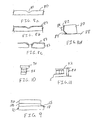
- FiGs. 8a-8d are schematic drawings illustrating creation and use of an electrical connection on the face of a substrate
- FIG. 9 is a schematic side view of another embodiment of electrical connections for the optical chassis.
- FIG. 10 is a schematic side view of the optical chassis with a larger optical element bonded thereto:
- FIG. 11 is a schematic side view of the optical chassis in a common housing with a larger optical element
- FIG. 12A is a schematic cross-section of a specific configuration of the optical chassis of the present invention inserted in a system
- FIG. 12B is a schematic cross-section of the specific configuration of the optical chassis of FIG. 12A alone;
- FIG. 13A is a schematic top view of alignment of the active optical element to the mirror
- FIG. 13B is a schematic side view of alignment of the active optical element to the mirror
- FIG. 14A is a schematic top view of alignment of the active optical element to the optics block.
- FIG. 14B is a schematic bottom view of alignment features of the optics block.
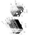
- FIG. 1 shows an embodiment of an optical chassis 5 of the present invention having four substrates. These four substrates include a mount substrate 10, a spacer substrate 20, a sealer substrate 30 and an optional optics substrate 40.
- the mount substrate 10 serves as a mount for optoelectronic devices, here a light source 12 and a power monitor 14, and provides the electrical interconnections, here including a wire bond 16, conductive patterns 17 and metalized trenches 18.
- the conductive patterns 17 each include a pad for the wire bond 16 and connect the pad to the trench 18 for external communication.
- the conductive patterns 17 may be created by patterning conductive material on the mount substrate 10 in a known manner.
- the trenches 18 may be created by removing a portion of the mount substrate 10 in a conventional manner and filling this portion with conductive material.
- the conductive material for the trenches 18 may be provided at the same time the conductive patterns 17 are formed.
- the details of the mount substrate 10 can be seen more clearly in FIG. 2 .
- the spacer substrate 20 provides room for the beam output from the light source 12 to expand. If the optoelectronic device 12 does not have its active area on its top face, e.g., an edge emitting laser, an appropriate portion of a sidewall 22 of the spacer substrate 20 may be angled and coated with a reflective coating to appropriately direct the beam in the optical chassis 5. A hole 24 in the spacer wafer 20 may be formed by etching a silicon wafer, producing the characteristic angled sidewall 22 from such an etch.
- the spacer substrate 20, in conjunction with the sealer substrate 30, hermetically seals and protects the optoelectronic devices 12, 14 from the environment.
- the sealer substrate 30 may also include an optical element on either surface thereof, e.g., an optical element which reduces the divergence of the beam output from the light source 12.
- the optional optics substrate 40 includes at least one optical element.
- a diffractive optical element 44 on a first surface of the optics substrate 40 directs some of the light from the light source 12 to the power monitor 14, as disclosed, for example, in commonly assigned U.S. Patent No. 6,314,223 entitled "Diffractive Vertical Cavity Surface Emitting Laser Power Monitor and System.”
- a coupling element 42 on a second surface of the optics substrate 40 may couple the light between the optoelectronic device, here the light source 12, and further applications, e.g., a fiber.
- more than one functionality may be incorporated into each optical element.
- a separation feature 32 e.g., an indentation or stand off, may be provided on either the sealer substrate 30 or the optional optics substrate 40 to insure proper functioning of the optical element.
- the sealer substrate 30 is transparent.
- the sealer substrate 30 may be glass or may be some other transparent material that closely matches the coefficient of thermal expansion of the spacer substrate 20, e.g., Pyrex when the spacer substrate is silicon.
- mating features may be provided on a terminal surface thereof.
- a standoff 43 encircling the optical element 42 may be provided.
- the standoff 43 may be SU-8 and provides both alignment of the optical chassis 5 with additional devices and provides separation of the optical element 42.
- a plurality of each of these substrates may be created on a wafer level, secured together with other substrates in a vertical stack, and then vertically separated to form a plurality of individual optical chassis 5.
- a mount wafer 10', a spacer wafer 20', a sealer wafer 30' and an optional optics wafer 40' are to be aligned and secured together on a wafer level.
- Each of these wafers includes a plurality of the respective mount substrates 10, spacer substrates 20, sealer substrates 30 and optional optical substrates 40.
- the top three wafers 40', 30' and 20' may be created completely on a wafer level in known fashions.
- These wafers may then be secured together as shown in FIG. 4 forming a secured stack wafer 50'.
- These wafers may be aligned and secured as set forth, for example, in U.S. Patent No. 6,096,155 entitled “Method of Dicing Wafer Level Integrated Optical Elements.”
- a plurality of metalized trenches 18 for providing the electrical interconnections may be formed on the wafer level.
- the optoelectronic elements 12, 14 may then be positioned on the mount wafer 10', e.g., using pick-and-place techniques, and then wire bonded 16 to the metalized trenches 18.
- the metalized trenches 18 may extend along the mount wafer 10', so the separation of the mount wafer 10' will expose the metal on the edge of the mount substrate, as can be seen In FIGS. 1 and 2 .
- the secured stack wafer 50' is then secured to the mount wafer 10' and then vertically separated to form a plurality of optical chassis 5 as shown in FIG. 1 .
- the secured stack wafer may be vertically separated to form secured stack substrates, which are then bonded to the mount wafer 10'.
- FIGS. 6 and 7 An alternative optical chassis 55 is shown in FIGS. 6 and 7 .
- the optional optical substrate 40 is not included. Only a diffractive optical element 34 for power monitoring and/or efficient coupling is provided on the sealer substrate 30.
- the spacer substrate 20 is the same as in FIG. 1 .
- the mount substrate 60 provides different electrical connections as in FIG. 1 for the light source 12 and the power monitor 14.
- the optoelectronic devices are again wire bonded, here to conductive pads 65.
- conductive, e.g., metalized, through holes or vias 64 and conductive structures 62, e.g., solder balls, are used to provide the electrical interconnections to the optical elements on the top surface of the mount substrate 60.
- FIGS. 8A-8D Another alternative for providing electrical interconnections to the optoelectronic element on a wafer level is shown in FIGS. 8A-8D .
- a saw or other etching device is used to produce V-shaped groove 81 In a wafer 80.
- the groove 81 and the wafer 80 are coated with an electrically conductive coating 82, e.g., metal, as shown in FIG. 8B .
- the wafer 80 is separated at the V-groove 81 and at another portion to form a mount substrate 83, as shown in FIG. 8C .
- the groove 81 needs to be wide enough so that an angle remains after separation. For example, if dicing is used as the separation technique, the groove will need to be wider than the blade width of the dicing saw.
- an optoelectronic device 86 is mounted on the conductive coating 82 of the mount substrate 83.
- a solder ball 84 or other conductive structure may then used to connect the conductive coating 82 to an electrical connection on a board 88.
- the other substrates 20, 30 and optionally 40 may be stacked over the mount substrate 83 as shown in the other configurations.
- Electrical input/output may also be realized as shown In FIG. 9 , in which the substrates forming the optical chassis do not have the same width, thereby forming a ledge 15, with the electrical connection being realized on a portion of the chassis 5 providing the ledge 15.
- the ledge 15 may be formed by having the mount substrate 10 extend further in at least one direction than the adjacent spacer substrate 20.
- the electrical contacts may be formed on the surface of the ledge or a portion of the ledge 15 may be removed to form the trenches 18 therein to increase the surface for electrical contact.
- Such a ledge may be formed by die bonding a secured stacked substrate having the spacer substrate 20 and the sealer substrate 30 to the mount substrate 10. Forming such a ledge on wafer level may be realized in a number of manners, including using dicing saws of different thicknesses and dicing through opposite surfaces, e.g., flipping the wafer after partial dicing, of the secured stacked wafer, including the mount wafer 10'.
- optical chassis of the present invention may be used to simply replace the conventional TO-can element and can have the conventional optics aligned thereto, as is currently done for the TO-can optoelectronics. Two manners of achieving this are shown in shown in FIGS. 10 and 11 .
- the vertically integrated optical chassis 55 of the present invention may have an optical element 90, Including optical elements larger in the x- and/or y-direction than the optical chassis 55, die-bonded thereto.
- the optical element 90 may be separate from but aligned with the optical chassis 55, here shown in a common housing 92. This separation reduces the alignment tolerances for the optical element 90.
- the sealer substrate 30 may still include optics thereon for improving the light from the fight source 12, e.g., collimating or at least reducing the divergence of the light.
- FIGS. 12A-12B A specific configuration of an optical chassis in accordance with the present invention is shown in FIGS. 12A-12B .
- an optical chassis 100 is attached to a flex lead 150, inserted into a magnet 160, on which a fiber stop 170 and then a fiber sleeve 180 is secured.
- This structure may be provided on a heat sink.
- the optical chassis 100 includes a mount substrate 110 having a ledge 115, a spacer substrate 120 and a sealer substrate 130.
- An optoelectronic device 112 and wire bonds 116 are on the mount substrate 110.
- the sealer substrate 130 Includes a lens 132 and an angled, reflective sidewall 122.
- the angled, reflective sidewall 122 serves as a mirror to direct light between the optoelectronic device 112 and the fiber in the fiber sleeve 180. If the active area or facet of the optoelectronic device is not on an edge thereof, this angled, reflective sidewall 122 is not needed.
- An additional spacer substrate 136 which may include additional spacing structures 138, separates the lens 132 from an isolator stack 140.
- the spacing structures 138 are used when a passive optical element is on one or more opposing surfaces in the stack and the surfaces would otherwise by flush at the passive optical element.
- the spacing structures may be integral with the surface or may be provided on the surface. Alternatively, these spacing structures may be on the sealer substrate 130.
- the electrical connection of the optoelectronic device 116 is realized using the ledge 115, as discussed in connection with FIG. 9 .
- the isolator stack 140 Includes a first polarizer 142, a Faraday rotator 144 and a second polarizer 146.
- the magnet 170 which may be a ring magnet, surrounds the isolator stack 140 when the optical chassis 100 is inserted as shown in FIG. 12A , thereby completing the isolator, If the Faraday rotator 144 is a latching type, then the speared magnet 170 is not needed.
- the active elements are secured to the mount substrate such that they remain secured and withstand subsequent processing, e.g., the securing of the substrate.
- the construction of the optical chassis of the present invention needs to be determined in an appropriate order, with the least robust technique being performed last.
- the materials used for the securing of the active elements, realizing the electrical connections and the securing of the substrates must be selected in accordance with the required order.
- the active elements may be secured on the mount substrate using a gold-tin (AuSn) solder and the substrates may then be secured using a material with a lower melting point, e.g., silver-tin (AgSn) solder.
- FIGS. 13A-14B Techniques for realizing alignment of the optical elements in the optical chassis are shown in FIGS. 13A-14B .
- characteristics e.g., lens thickness, radius of curvature (ROC), of individual elements.
- ROC radius of curvature
- the variation in ROC may be compensated for with the placement of the angled surface 122 of the spacer substrate 120, as shown in FIG. 13A-13B .
- the separation d between the optoelectronic device 112 and a back edge of the angled surface 122 is determined in accordance with the ROC of the lens to be used. If the angled surface 122 has an angle of approximately 45°, this distance d will be roughly equal to the height of the spacer substrate 120. Thus, this aligning of the optoelectronic device 112 with the angled surface 122 compensates for any variations In the thickness of the spacer substrate 120, as well as taking the ROC of the lens into account.
- the aligning of the lens to the optoelectronic device 112 is shown in FIGS. 14A-14B .
- the image of the active area of the optoelectronic device 112 in the reflective angled surface 122 may be used to align the lens.
- a bottom surface of the substrate having the lens thereon which may be the sealer substrate 130 as shown in FIGS. 12A-12B , includes alignment features 134, here in the form of a crosshair centered on the lens on the top surface of the substrate.
- the alignment features 134 are then centered with the image of the active area of the optoelectronic device 112 as reflected by the angled surface 122 to insure proper alignment there between. Since the height of the optoelectronic element changes its location on the angled surface 122, by aligning the lens to the reflection from the angled surface 122, variations in the height of the optoelectronic element may be compensated for as well.
- the lens may be aligned by directly viewing the active area using alignment features 134.
- the alignment thereof is not critical. Since the sealer substrate 130 is transparent, alignment features do not need to be provided thereon, as alignment features on surfaces below the sealer substrate may be viewed through it. If there are optical elements on other substrates, and the sealer substrate 130 is transparent, the same alignment techniques may be employed.
- an optical chassis having a small form factor may be created at least partially on a wafer level, including electrical interconnections.
- the optical chassis of the present Invention also provides a hermetic seal without requiring a TO can or other separate housing. Further, since substrates of the optical chassis are secured to one another, rather than to a carrier as in a TO can, better alignment can be maintained for longer.
- any of the electrical interconnections shown may be used with any optical chassis embodiments.
- additional optical substrates or elements as needed may be secured to the optical chassis.
- any of the configurations of the optical chassis may be created at least partially on a wafer level as discussed regarding FIGS. 3-5 .
- the present invention may be characterised by the following points;
Abstract
Description
- The present invention is directed to a wafer based optical chassis and associated methods. More particularly, the present invention is directed to protecting active elements in an optical system and realizing electrical input/output without requiring separate packaging.
- Active elements, such as optoelectronic chips, e.g., light sources for transmitters and detectors for receivers, are typically housed in a transistor outline (TO) can. Such a TO can is typically made of metal, has a large form factor, involves an expensive serial manufacturing process and requires active alignment with external passive optical elements. This large form factor separates the active element from an external passive optic along the optical axis, resulting in the passive optic needing to handle a more divergent beam, rendering the optic bigger, thereby further increasing the size of the system. Additionally, the TO can has electrical termination concerns, limiting the speed of the active elements.
- Current trends towards miniaturization have spurred numerous small form factor designs. Most of these designs are directed to integrating the passive optical element with some connector, separate from the TO can. While this may reduce the length of the system and simplify the manufacturing of the passive optical portion of the system, the TO can, and the problems attendant therewith, are still present.
- The present invention is therefore directed to a wafer based optical chassis and associated methods that substantially overcome one or more of the problems due to the limitations and disadvantages of the related art.
- It is a feature of the present invention to protect an active element with an assembly including passive optical elements. It is another feature of the present invention to provide efficient electrical coupling to and from the protected active elements. It is yet another feature of the present invention to provide hermetic packaging of an active element that can at least partially be created in parallel. It is yet another feature of the present Invention to provide alignment that compensates for variations arising In the manufacturing process.
- At least one of the above and other features may be realized by providing an optical apparatus Including a mount substrate, an optoelectronic device on the mount substrate, a spacer substrate and a sealer substrate. The mount substrate, the spacer substrate and the sealer substrate are vertically stacked and hermetically seal the optoelectronic device. The apparatus also Includes external electrical contact for the optoelectronic device outside the sealing.
- An interior surface of the spacer substrate may be angled and have a reflective material thereon. The electrical contact may include a metalized trench. The mount substrate and the spacer substrate may be flush. The optical apparatus as may include a ledge formed by differing widths between the mount substrate and the spacer substrate. The metalized trenches may be in the ledge or the electrical contact may be on the ledge. The electrical contact may include a conductive via on a bottom surface of the mount substrate and a conductive structure In the via. The conductive structure is a solder ball. The electrical contact may include a conductive material on at least two non-parallel surfaces of the mount substrate.
- A passive optical element may be on a surface of the sealer substrate. The optical apparatus may include, above the sealer substrate, an optical block having a passive optical element on at least one surface thereof. The optical apparatus may Include, above the sealer substrate, an isolator stack Including first and second polarizers and a Faraday rotator sandwiched between the first and second polarizers. The optical apparatus may Include, above the sealer substrate, another spacer substrate. At least two of the mount substrate, the spacer substrate and the sealer substrate are of materials with approximately same coefficients of thermal expansion. One of the at least two substrates may be silicon and the other may be Pyrex. A terminal surface of the optical apparatus may include a mating feature for mating the optical apparatus with another structure, e.g., a ferrule.
- At least one of the above and other features may be realized by providing a method of aligning an active device and a lens, including providing the active device on a mount substrate, the active device having an active area on a side thereof, positioning an angled reflector relative to the active area in accordance with a radius of curvature of the lens, viewing the active area reflected by the angled reflector, and positioning the lens In accordance with the viewed active area.
- At least one of the above and other features may be realized by providing a method of creating a plurality of optical apparatuses, including patterning a conductive material on a mount wafer, populating the mount substrate with optoelectronic devices in accordance with the patterning, stacking and securing a spacer substrate on the mount wafer, stacking and securing a sealer substrate on the spacer substrate, wherein the stacking and securing of the spacer substrate and the sealer substrate on the mount wafer hermetically seal the optoelectronic devices, and vertically separating the mount wafer to form the plurality of optical apparatuses. The vertically separating including exposing a portion of the conductive material outside the hermetic seal. Each optical apparatus includes a mount substrate, an optoelectronic device, a spacer substrate, a sealer substrate, and exposed conductive material.
- The stacking and securing of the sealer substrate to the spacer substrate occurs before stacking and securing of the spacer substrate stacked to the mount substrate.
- The above and other features and advantages of the present invention will become readily apparent to those of skill in the art by describing in detail embodiments thereof with reference to the attached drawings, in which:
-
FIG. 1 is an elevational perspective view of an embodiment of the optical chassis of the present invention; -
FIG. 2 is a detailed elevational perspective view of the optoelectronic devices and electrical interconnections of the optical chassis ofFIG. 1 ; -
FIG. 3 is an elevational perspective exploded view of the wafer components to be used to create the optical chassis ofFIG. 1 ; -
FIG. 4 is an elevational perspective view of the passive optical element wafers ofFIG. 3 secured together; -
FIG. 5 is an elevational perspective view of the active element wafer to be bonded to the stack of wafers inFIG. 4 and then vertically separated to form the optical chassis ofFIG. 1 ; -
FIG. 6 an elevational perspective view of another embodiment of the optical chassis of the present invention; -
FIG. 7 is a detailed perspective bottom view of the electrical interconnections of the optical chassis shown inFIG. 6 ; -
FiGs. 8a-8d are schematic drawings illustrating creation and use of an electrical connection on the face of a substrate; -
FIG. 9 is a schematic side view of another embodiment of electrical connections for the optical chassis; -
FIG. 10 is a schematic side view of the optical chassis with a larger optical element bonded thereto: -
FIG. 11 is a schematic side view of the optical chassis in a common housing with a larger optical element; -
FIG. 12A is a schematic cross-section of a specific configuration of the optical chassis of the present invention inserted in a system; -
FIG. 12B is a schematic cross-section of the specific configuration of the optical chassis ofFIG. 12A alone; -
FIG. 13A is a schematic top view of alignment of the active optical element to the mirror; -
FIG. 13B is a schematic side view of alignment of the active optical element to the mirror; -
FIG. 14A is a schematic top view of alignment of the active optical element to the optics block; and -
FIG. 14B is a schematic bottom view of alignment features of the optics block. - The present invention will now be described more fully hereinafter with reference to the accompanying drawings, in which exemplary embodiments of the invention are shown. The invention may, however, be embodied in different forms and should not be construed as limited to the embodiments set forth herein. Rather, these embodiments are provided so that this disclosure will be thorough and complete, and will fully convey the concept of the invention to those skilled in the art. In the drawings, the thickness of layers and regions are exaggerated for clarity. It will also be understood that when a layer is referred to as being "on" another layer or substrate, it may be directly on the other layer or substrate, or intervening layers may also be present. Further, it will be understood that when a layer is referred to as being "under" another layer, it may be directly under, or one or more intervening layers may also be present. In addition, it will also be understood that when a layer is referred to as being "between" two layers, it may be the only layer between the two layers, or one or more intervening layers may also be present. Like numbers refer to like elements throughout.
-
FIG. 1 shows an embodiment of an optical chassis 5 of the present invention having four substrates. These four substrates include amount substrate 10, aspacer substrate 20, asealer substrate 30 and anoptional optics substrate 40. Themount substrate 10 serves as a mount for optoelectronic devices, here alight source 12 and apower monitor 14, and provides the electrical interconnections, here including awire bond 16, conductive patterns 17 and metalizedtrenches 18. The conductive patterns 17 each include a pad for thewire bond 16 and connect the pad to thetrench 18 for external communication. The conductive patterns 17 may be created by patterning conductive material on themount substrate 10 in a known manner. Thetrenches 18 may be created by removing a portion of themount substrate 10 in a conventional manner and filling this portion with conductive material. The conductive material for thetrenches 18 may be provided at the same time the conductive patterns 17 are formed. The details of themount substrate 10 can be seen more clearly inFIG. 2 . - The
spacer substrate 20 provides room for the beam output from thelight source 12 to expand. If theoptoelectronic device 12 does not have its active area on its top face, e.g., an edge emitting laser, an appropriate portion of asidewall 22 of thespacer substrate 20 may be angled and coated with a reflective coating to appropriately direct the beam in the optical chassis 5. Ahole 24 in thespacer wafer 20 may be formed by etching a silicon wafer, producing the characteristicangled sidewall 22 from such an etch. Thespacer substrate 20, in conjunction with thesealer substrate 30, hermetically seals and protects theoptoelectronic devices sealer substrate 30 may also include an optical element on either surface thereof, e.g., an optical element which reduces the divergence of the beam output from thelight source 12. - The
optional optics substrate 40 includes at least one optical element. Here, a diffractiveoptical element 44 on a first surface of theoptics substrate 40 directs some of the light from thelight source 12 to thepower monitor 14, as disclosed, for example, in commonly assignedU.S. Patent No. 6,314,223 entitled "Diffractive Vertical Cavity Surface Emitting Laser Power Monitor and System." Acoupling element 42 on a second surface of theoptics substrate 40 may couple the light between the optoelectronic device, here thelight source 12, and further applications, e.g., a fiber. Of course, more than one functionality may be incorporated into each optical element. - If an optical element is to be provided on one or both of the surfaces of the optional
optical substrate 40 or thesealer substrate 30 adjacent to one another, a separation feature 32, e.g., an indentation or stand off, may be provided on either thesealer substrate 30 or theoptional optics substrate 40 to insure proper functioning of the optical element. Thesealer substrate 30 is transparent. Thesealer substrate 30 may be glass or may be some other transparent material that closely matches the coefficient of thermal expansion of thespacer substrate 20, e.g., Pyrex when the spacer substrate is silicon. The smaller size of the chassis 5, e.g., roughly 2mm by 2mm In x and y, also helps with any thermal mismatch, since there is not a lot of strain placed in the securing joints between the substrates. - Finally, when the optical chassis 5 Is to be joined with another device, mating features may be provided on a terminal surface thereof. For example, if the optical chassis is to be mated with a fiber optic ferule, a
standoff 43 encircling theoptical element 42 may be provided. Thestandoff 43 may be SU-8 and provides both alignment of the optical chassis 5 with additional devices and provides separation of theoptical element 42. - As can be seen from the profile of the optical chassis 5, a plurality of each of these substrates may be created on a wafer level, secured together with other substrates in a vertical stack, and then vertically separated to form a plurality of individual optical chassis 5. As shown in
FIG. 3 , a mount wafer 10', a spacer wafer 20', a sealer wafer 30' and an optional optics wafer 40' are to be aligned and secured together on a wafer level. Each of these wafers includes a plurality of therespective mount substrates 10,spacer substrates 20,sealer substrates 30 and optionaloptical substrates 40. The top three wafers 40', 30' and 20' may be created completely on a wafer level in known fashions. These wafers may then be secured together as shown inFIG. 4 forming a secured stack wafer 50'. These wafers may be aligned and secured as set forth, for example, inU.S. Patent No. 6,096,155 entitled "Method of Dicing Wafer Level Integrated Optical Elements." - For the mount wafer 10', a plurality of metalized
trenches 18 for providing the electrical interconnections may be formed on the wafer level. Theoptoelectronic elements trenches 18. The metalizedtrenches 18 may extend along the mount wafer 10', so the separation of the mount wafer 10' will expose the metal on the edge of the mount substrate, as can be seen InFIGS. 1 and 2 . The secured stack wafer 50' is then secured to the mount wafer 10' and then vertically separated to form a plurality of optical chassis 5 as shown inFIG. 1 . Alternatively, the secured stack wafer may be vertically separated to form secured stack substrates, which are then bonded to the mount wafer 10'. - An alternative
optical chassis 55 is shown inFIGS. 6 and 7 . Here, the optionaloptical substrate 40 is not included. Only a diffractiveoptical element 34 for power monitoring and/or efficient coupling is provided on thesealer substrate 30. Thespacer substrate 20 is the same as inFIG. 1 . Themount substrate 60 provides different electrical connections as inFIG. 1 for thelight source 12 and thepower monitor 14. Here, the optoelectronic devices are again wire bonded, here toconductive pads 65. Then, on the bottom of themount substrate 60, conductive, e.g., metalized, through holes orvias 64 andconductive structures 62, e.g., solder balls, are used to provide the electrical interconnections to the optical elements on the top surface of themount substrate 60. These conductive structures must be large enough to obscure the hole in the mount substrate to Insure the hermetic seal, to avoid creating a thermal gradient and to avoid extra oxidation. This solution is particularly useful If the mount substrate is a ceramic, since it is expensive to put solder on ceramic. - Another alternative for providing electrical interconnections to the optoelectronic element on a wafer level is shown in
FIGS. 8A-8D . As shown InFIG. 8A , a saw or other etching device is used to produce V-shaped groove 81 In awafer 80. Then, the groove 81 and thewafer 80 are coated with an electricallyconductive coating 82, e.g., metal, as shown inFIG. 8B . Then, thewafer 80 is separated at the V-groove 81 and at another portion to form amount substrate 83, as shown inFIG. 8C . The groove 81 needs to be wide enough so that an angle remains after separation. For example, if dicing is used as the separation technique, the groove will need to be wider than the blade width of the dicing saw. - As shown in
FIG. 8D , an optoelectronic device 86 is mounted on theconductive coating 82 of themount substrate 83. Asolder ball 84 or other conductive structure may then used to connect theconductive coating 82 to an electrical connection on a board 88. Theother substrates mount substrate 83 as shown in the other configurations. - Electrical input/output may also be realized as shown In
FIG. 9 , in which the substrates forming the optical chassis do not have the same width, thereby forming aledge 15, with the electrical connection being realized on a portion of the chassis 5 providing theledge 15. As shown inFIG. 9 , theledge 15 may be formed by having themount substrate 10 extend further in at least one direction than theadjacent spacer substrate 20. The electrical contacts may be formed on the surface of the ledge or a portion of theledge 15 may be removed to form thetrenches 18 therein to increase the surface for electrical contact. - Such a ledge may be formed by die bonding a secured stacked substrate having the
spacer substrate 20 and thesealer substrate 30 to themount substrate 10. Forming such a ledge on wafer level may be realized in a number of manners, including using dicing saws of different thicknesses and dicing through opposite surfaces, e.g., flipping the wafer after partial dicing, of the secured stacked wafer, including the mount wafer 10'. - If customized performance of the optical chassis is known, optional optical substrate(s) may be Incorporated to provide the desired performance.
Otherwise, the optical chassis of the present invention may be used to simply replace the conventional TO-can element and can have the conventional optics aligned thereto, as is currently done for the TO-can optoelectronics. Two manners of achieving this are shown in shown inFIGS. 10 and 11 . As shown inFIG. 10 , the vertically integratedoptical chassis 55 of the present invention may have anoptical element 90, Including optical elements larger in the x- and/or y-direction than theoptical chassis 55, die-bonded thereto. As shown inFIG. 11 , theoptical element 90 may be separate from but aligned with theoptical chassis 55, here shown in acommon housing 92. This separation reduces the alignment tolerances for theoptical element 90. Thesealer substrate 30 may still include optics thereon for improving the light from thefight source 12, e.g., collimating or at least reducing the divergence of the light. - A specific configuration of an optical chassis in accordance with the present invention is shown in
FIGS. 12A-12B . As can be seen therein, an optical chassis 100 is attached to aflex lead 150, inserted into a magnet 160, on which a fiber stop 170 and then a fiber sleeve 180 is secured. This structure may be provided on a heat sink. - The optical chassis 100 includes a
mount substrate 110 having aledge 115, aspacer substrate 120 and asealer substrate 130. Anoptoelectronic device 112 andwire bonds 116 are on themount substrate 110. Thesealer substrate 130 Includes alens 132 and an angled,reflective sidewall 122. The angled,reflective sidewall 122 serves as a mirror to direct light between theoptoelectronic device 112 and the fiber in the fiber sleeve 180. If the active area or facet of the optoelectronic device is not on an edge thereof, this angled,reflective sidewall 122 is not needed. - An
additional spacer substrate 136, which may include additional spacing structures 138, separates thelens 132 from anisolator stack 140. The spacing structures 138 are used when a passive optical element is on one or more opposing surfaces in the stack and the surfaces would otherwise by flush at the passive optical element. The spacing structures may be integral with the surface or may be provided on the surface. Alternatively, these spacing structures may be on thesealer substrate 130. The electrical connection of theoptoelectronic device 116 is realized using theledge 115, as discussed in connection withFIG. 9 . - The
isolator stack 140 Includes afirst polarizer 142, aFaraday rotator 144 and asecond polarizer 146. The magnet 170, which may be a ring magnet, surrounds theisolator stack 140 when the optical chassis 100 is inserted as shown inFIG. 12A , thereby completing the isolator, If theFaraday rotator 144 is a latching type, then the speared magnet 170 is not needed. - In any of the above configurations, the active elements are secured to the mount substrate such that they remain secured and withstand subsequent processing, e.g., the securing of the substrate. The construction of the optical chassis of the present invention needs to be determined in an appropriate order, with the least robust technique being performed last. The materials used for the securing of the active elements, realizing the electrical connections and the securing of the substrates must be selected in accordance with the required order. For example, the active elements may be secured on the mount substrate using a gold-tin (AuSn) solder and the substrates may then be secured using a material with a lower melting point, e.g., silver-tin (AgSn) solder.
- Techniques for realizing alignment of the optical elements in the optical chassis are shown in
FIGS. 13A-14B . In making micro-optical elements, there are inevitable variations in characteristics, e.g., lens thickness, radius of curvature (ROC), of individual elements. By classifying these lenses by their ROC into different groups within a range, e.g., ±1%, the variation in ROC may be compensated for with the placement of theangled surface 122 of thespacer substrate 120, as shown inFIG. 13A-13B . Once a lens is selected for a particularoptoelectronic device 112 on themount substrate 110, the separation d between theoptoelectronic device 112 and a back edge of theangled surface 122 is determined in accordance with the ROC of the lens to be used. If theangled surface 122 has an angle of approximately 45°, this distance d will be roughly equal to the height of thespacer substrate 120. Thus, this aligning of theoptoelectronic device 112 with theangled surface 122 compensates for any variations In the thickness of thespacer substrate 120, as well as taking the ROC of the lens into account. - The aligning of the lens to the
optoelectronic device 112 is shown inFIGS. 14A-14B . Here, the image of the active area of theoptoelectronic device 112 in the reflectiveangled surface 122 may be used to align the lens. A bottom surface of the substrate having the lens thereon, which may be thesealer substrate 130 as shown inFIGS. 12A-12B , includes alignment features 134, here in the form of a crosshair centered on the lens on the top surface of the substrate. The alignment features 134 are then centered with the image of the active area of theoptoelectronic device 112 as reflected by theangled surface 122 to insure proper alignment there between. Since the height of the optoelectronic element changes its location on theangled surface 122, by aligning the lens to the reflection from theangled surface 122, variations in the height of the optoelectronic element may be compensated for as well. - If the active area of the
optoelectronic device 112 is not on a side thereof, the lens may be aligned by directly viewing the active area using alignment features 134. The variation in height of such optoelectronic devices, I.e., in the z-direction, do not significantly affect the performance. If there are no optical elements on thesealer substrate 130, the alignment thereof is not critical. Since thesealer substrate 130 is transparent, alignment features do not need to be provided thereon, as alignment features on surfaces below the sealer substrate may be viewed through it. If there are optical elements on other substrates, and thesealer substrate 130 is transparent, the same alignment techniques may be employed. - Thus, in accordance with the present invention, an optical chassis having a small form factor may be created at least partially on a wafer level, including electrical interconnections. The optical chassis of the present Invention also provides a hermetic seal without requiring a TO can or other separate housing. Further, since substrates of the optical chassis are secured to one another, rather than to a carrier as in a TO can, better alignment can be maintained for longer.
- While the present invention is described herein with reference to illustrative embodiments for particular applications, it should be understood that the present invention is not limited thereto. Those having ordinary skill in the art and access to the teachings provided herein will recognize additional modifications, applications, and embodiments within the scope thereof and additional fields in which the invention would be of significant utility without undue experimentation. For example, any of the electrical interconnections shown may be used with any optical chassis embodiments. Further, additional optical substrates or elements as needed may be secured to the optical chassis. Finally, any of the configurations of the optical chassis may be created at least partially on a wafer level as discussed regarding
FIGS. 3-5 . - The present invention may be characterised by the following points;
- 1. An optical apparatus, comprising:
- a mount substrate;
- an optoelectronic device on the mount substrate;
- a spacer substrate;
- a sealer substrate, the mount substrate, the spacer substrate and the sealer substrate being vertically stacked and hermetically sealing the optoelectronic device; and
- external electrical contact for the optoelectronic device provided outside the sealing.
- 2. The optical apparatus as in point 1, wherein an interior surface of the spacer substrate is angled and has a reflective material thereon.
- 3. The optical apparatus as claimed In claim 1, wherein the electrical contact includes a metalized trench.
- 4. The optical apparatus as in point 3, wherein the mount substrate and the spacer substrate are flush.
- 5. The optical apparatus as in point 3, further comprising a ledge formed by differing widths between the mount substrate and the spacer substrate, the metalized trenches being in the ledge.
- 6. The optical apparatus as in point 1, further comprising a ledge formed by differing widths between the mount substrate and the spacer substrate, the electrical contact for the optoelectronic device being on the ledge.
- 7. The optical apparatus as in point 1, wherein the electrical contact further comprises:
- a conductive via on a bottom surface of the mount substrate; and
- a conductive structure in the via.
- 8. The optical apparatus as in point 7, wherein the conductive structure is a solder ball.
- 9. The optical apparatus as in point 1, further comprising a passive optical element formed on a surface of the sealer substrate.
- 10. The optical apparatus as in point 1, wherein electrical contact further comprises a conductive material on at least two non-parallel surfaces of the mount substrate.
- 11. The optical apparatus as in point 1, further comprising, above the sealer substrate, an optical block having a passive optical element on at least one surface thereof.
- 12. The optical apparatus as in point 1, further comprising, above the sealer substrate, an isolator stack including first and second polarizers and a Faraday rotator sandwiched between the first and second polarizers.
- 13. The optical apparatus as in point 1, further comprising, above the sealer substrate, another spacer substrate.
- 14. The optical apparatus as in point 1, wherein at least two of the mount substrate, the spacer substrate and the sealer substrate are of materials with approximately same coefficients of thermal expansion.
- 15. The optical apparatus as in
point 14, wherein one of the at least two substrates is silicon and another of the at least two substrate is Pyrex. - 16. The optical apparatus as in point 1, further comprising, on a terminal surface of the optical apparatus, a mating feature for mating the optical apparatus with another structure.
- 17. The optical apparatus as in
point 16, wherein the another structure is a ferrule. - 18. A method of aligning an active device and a lens, comprising:
- providing the active device on a mount substrate, the active device having an active area on a side thereof;
- positioning an angled reflector relative to the active area in accordance with a radius of curvature of the lens;
- viewing the active area reflected by the angled reflector;
- positioning the lens in accordance with the viewed active area.
- 19. A method of creating a plurality of optical apparatuses, comprising:
- patterning a conductive material on a mount Wafer;
- populating the mount substrate with optoelectronic devices in accordance with the patterning;
- stacking and securing a spacer substrate on the mount wafer;
- stacking and securing a sealer substrate on the spacer substrate, wherein the stacking and securing of the spacer substrate and the sealer substrate on the mount wafer hermetically seal the optoelectronic devices; and
- vertically separating the mount wafer to form the plurality of optical apparatuses, the vertically separating including exposing a portion of the conductive material outside the hermetic seal, each optical apparatus includes a mount substrate, an optoelectronic device, a spacer substrate, a sealer substrate, and exposed conductive material.
- 20. The method as in point 19, wherein stacking and securing of the sealer substrate to the spacer substrate occurs before stacking and securing of the spacer substrate stacked to the mount substrate.
Claims (15)
- An optical apparatus, comprising:a mount substrate (10);an optoelectronic device (12) on the mount substrate (10);a spacer layer (20) on the mount substrate (10). the spacer including a hole exposing the optoelectronic device;a sealer layer (30) on the spacer layer (20), the cover layer (30) covering the hole, the mount substrate (10), the spacer layer (20) and the sealer layer (30) together sealing the optoelectronic device (12), the sealer layer (30) having a planar surface facing the optoelectronic device (12); andan external electrical interconnection (18, 62, 64) for the optoelectronic device (12) provided outside the sealing, the external electrical interconnection being on a first surface and a second surface, different from the first surface, of the mount substrate (10), the external electrical interconnection (18, 62, 64) adapted to connect the optoelectronic device (12) to an electrical contact pad.
- The optical apparatus as claimed in claim 1, wherein the mount substrate (10) and the spacer layer (20) are horizontally co-extensive.
- The optical apparatus as claimed in claim 1, further comprising a via (64) extending through a bottom surface of the mount substrate (10), the bottom surface serving as the second surface, the external electrical interconnection (18, 62, 64) going through the via (64) and connecting the optoelectronic device (12) on the first surface of the mount substrate (10) to the electrical contact pad adjacent the bottom surface of the mount substrate (10).
- The optical apparatus as claimed in claim 1, wherein the mount substrate (110) is a detector chip and an active area of the detector chip is integrated in the first surface of the mount substrate (110).
- The optical apparatus as claimed in claim 1, further comprising an optical element (44) on a substrate (40), substantially planar regions of the substrate (40) being secured to the sealer layer (30).
- The optical apparatus as claimed in claim 7, further comprising a spacer feature (32) between the substrate (40) and the sealer layer (30), the spacer feature (32) includes an aperture.
- A method of forming an optical apparatus, comprising:providing a mount substrate (10);providing an optoelectronic device (12) on the mount substrate (10);providing a spacer layer (20) on the mount substrate (10), the spacer including a hole exposing the optoelectronic device;providing a sealer layer (30) on the spacer layer (20), the cover layer (30) covering the hole, the mount substrate (10), the spacer layer (20) and the sealer layer (30) together sealing the optoelectronic device (12), the sealer layer (30) having a planar surface facing the optoelectronic device (12); andproviding an external electrical interconnection (18, 62, 64) for the optoelectronic device (12) provided outside the sealing, the external electrical interconnection being on a first surface and a second surface, different from the first surface, of the mount substrate (10), the external electrical interconnection (18, 62, 64) adapted to connect the optoelectronic device (12) to an electrical contact pad.
- The method as claimed in claim 7, wherein providing external electrical interconnection (18, 62, 64) comprises providing a via (64) extending through a bottom surface of the mount substrate (10), the bottom surface serving as the second surface, the external electrical interconnection going through the via (64) and connecting the optoelectronic device (12) on the first surface of the mount substrate (10) to the electrical contact pad adjacent the bottom surface of the mount substrate (10).
- The method as claimed in claim 7, wherein providing an optoelectronic device (12) on the mount substrate (10) includes integrating an active area of the optoelectronic device (12) in the first surface of the mount substrate (10).
- The method as claimed in claim 7, further comprising:providing an optical element (44) on a substrate (40); andsecuring substantially planar regions of the substrate (40) to the sealer layer (30).
- The method as claimed in claim 10, further comprising:providing a spacer feature (32) between the substrate (40) and the sealer layer (30); andsecuring at least three of the mount substrate (10), the spacer layer (20), the sealer layer (30), the substrate (40), and the spacer feature (32) at a wafer level.
- An optical apparatus, comprising:an upper layer (136);a middle layer (130);a first spacer structure (138) between the upper (136) and middle layers (130), the upper (136) and middle layers (130) and a first spacer structure (138) defining a first interior space;a lower substrate (110);a second layer (120) between the middle layer (130) and the lower substrate (110), the middle layer (130), the lower substrate (110) and the second spacer layer (120) defining a second interior space;a passive optical element (132) on the middle layer (130), the passive optical element (132) being in one of the first and second interior spaces;an optoelectronic device (112) on the lower substrate (110) in the second interior space; andan external electrical interconnection (18, 62, 64) for the optoelectronic device (112) on the lower substrate (110) outside the second interior space.
- The optical apparatus as claimed in claim 12, wherein the lower substrate (110) is a detector chip and an active area of the detector chip is integrated in the first surface of the mount substrate (110).
- A method of making an optical apparatus, comprising:providing an upper layer (136);providing a middle layer (130);providing a spacing structure (138) between the upper (136) and middle layers (130), the upper (136) and middle layers (130) and a first spacer structure (138) defining a first interior space;providing a lower substrate (110);providing a spacer layer (120) between the middle layer (130) and the lower substrate (110), the middle layer (130), the lower substrate (110) and the second spacer layer (120) defining a second interior space;providing a passive optical element (132) on the middle layer (130), the passive optical element (132) being in one of the first and second interior spaces;providing an optoelectronic device (112) on the lower substrate (110) in the second interior space; andproviding an external electrical interconnection (18, 62, 64) for the optoelectronic device (112) on the lower substrate (110) outside the second interior space.
- The method as claimed in claim 28, further comprising securing at least three of the upper layer (136), the spacing structure (138), the spacer layer (120) and the lower substrate (110) at a wafer level.
Applications Claiming Priority (2)
| Application Number | Priority Date | Filing Date | Title |
|---|---|---|---|
| US45766403P | 2003-03-26 | 2003-03-26 | |
| EP04758439A EP1611468B1 (en) | 2003-03-26 | 2004-03-26 | Package for optoelectronic device on wafer level |
Related Parent Applications (2)
| Application Number | Title | Priority Date | Filing Date |
|---|---|---|---|
| EP04758439.6 Division | 2004-03-26 | ||
| EP04758439A Division EP1611468B1 (en) | 2003-03-26 | 2004-03-26 | Package for optoelectronic device on wafer level |
Publications (3)
| Publication Number | Publication Date |
|---|---|
| EP1953577A2 true EP1953577A2 (en) | 2008-08-06 |
| EP1953577A3 EP1953577A3 (en) | 2010-06-16 |
| EP1953577B1 EP1953577B1 (en) | 2013-07-17 |
Family
ID=33131703
Family Applications (2)
| Application Number | Title | Priority Date | Filing Date |
|---|---|---|---|
| EP04758439A Expired - Lifetime EP1611468B1 (en) | 2003-03-26 | 2004-03-26 | Package for optoelectronic device on wafer level |
| EP08009231.5A Expired - Lifetime EP1953577B1 (en) | 2003-03-26 | 2004-03-26 | Package for optoelectronic device on wafer level |
Family Applications Before (1)
| Application Number | Title | Priority Date | Filing Date |
|---|---|---|---|
| EP04758439A Expired - Lifetime EP1611468B1 (en) | 2003-03-26 | 2004-03-26 | Package for optoelectronic device on wafer level |
Country Status (6)
| Country | Link |
|---|---|
| EP (2) | EP1611468B1 (en) |
| AT (1) | ATE396418T1 (en) |
| CA (1) | CA2523418C (en) |
| DE (1) | DE602004013945D1 (en) |
| DK (1) | DK1611468T3 (en) |
| WO (1) | WO2004088380A2 (en) |
Citations (2)
| Publication number | Priority date | Publication date | Assignee | Title |
|---|---|---|---|---|
| US6096155A (en) | 1996-09-27 | 2000-08-01 | Digital Optics Corporation | Method of dicing wafer level integrated multiple optical elements |
| US6314223B1 (en) | 1998-08-31 | 2001-11-06 | Digital Optics Corporation | Diffractive vertical cavity surface emitting laser power monitor and system |
Family Cites Families (10)
| Publication number | Priority date | Publication date | Assignee | Title |
|---|---|---|---|---|
| US4873566A (en) * | 1985-10-28 | 1989-10-10 | American Telephone And Telegraph Company | Multilayer ceramic laser package |
| US5011256A (en) * | 1988-10-28 | 1991-04-30 | E. I. Du Pont De Nemours And Company | Package for an opto-electronic component |
| TW272311B (en) * | 1994-01-12 | 1996-03-11 | At & T Corp | |
| US5886971A (en) * | 1996-09-27 | 1999-03-23 | Digital Optics Corporation | Optical head structures including support substrates adjacent transparent substrates and related methods |
| US5912872A (en) * | 1996-09-27 | 1999-06-15 | Digital Optics Corporation | Integrated optical apparatus providing separated beams on a detector and associated methods |
| US6981804B2 (en) * | 1998-06-08 | 2006-01-03 | Arrayed Fiberoptics Corporation | Vertically integrated optical devices coupled to optical fibers |
| US6249136B1 (en) * | 1999-06-28 | 2001-06-19 | Advanced Micro Devices, Inc. | Bottom side C4 bumps for integrated circuits |
| US6351027B1 (en) * | 2000-02-29 | 2002-02-26 | Agilent Technologies, Inc. | Chip-mounted enclosure |
| US6492699B1 (en) * | 2000-05-22 | 2002-12-10 | Amkor Technology, Inc. | Image sensor package having sealed cavity over active area |
| US6798931B2 (en) * | 2001-03-06 | 2004-09-28 | Digital Optics Corp. | Separating of optical integrated modules and structures formed thereby |
-
2004
- 2004-03-26 EP EP04758439A patent/EP1611468B1/en not_active Expired - Lifetime
- 2004-03-26 DE DE602004013945T patent/DE602004013945D1/en not_active Expired - Lifetime
- 2004-03-26 EP EP08009231.5A patent/EP1953577B1/en not_active Expired - Lifetime
- 2004-03-26 AT AT04758439T patent/ATE396418T1/en not_active IP Right Cessation
- 2004-03-26 WO PCT/US2004/009383 patent/WO2004088380A2/en active Application Filing
- 2004-03-26 DK DK04758439T patent/DK1611468T3/en active
- 2004-03-26 CA CA2523418A patent/CA2523418C/en not_active Expired - Lifetime
Patent Citations (2)
| Publication number | Priority date | Publication date | Assignee | Title |
|---|---|---|---|---|
| US6096155A (en) | 1996-09-27 | 2000-08-01 | Digital Optics Corporation | Method of dicing wafer level integrated multiple optical elements |
| US6314223B1 (en) | 1998-08-31 | 2001-11-06 | Digital Optics Corporation | Diffractive vertical cavity surface emitting laser power monitor and system |
Also Published As
| Publication number | Publication date |
|---|---|
| WO2004088380A2 (en) | 2004-10-14 |
| WO2004088380A3 (en) | 2005-04-21 |
| EP1953577B1 (en) | 2013-07-17 |
| ATE396418T1 (en) | 2008-06-15 |
| EP1611468A2 (en) | 2006-01-04 |
| CA2523418C (en) | 2011-05-03 |
| DE602004013945D1 (en) | 2008-07-03 |
| EP1953577A3 (en) | 2010-06-16 |
| DK1611468T3 (en) | 2008-09-08 |
| CA2523418A1 (en) | 2004-10-14 |
| EP1611468B1 (en) | 2008-05-21 |
Similar Documents
| Publication | Publication Date | Title |
|---|---|---|
| US7751659B2 (en) | Optical apparatus | |
| US7961989B2 (en) | Optical chassis, camera having an optical chassis, and associated methods | |
| US9442255B2 (en) | Low profile fiber-to-module interface with relaxed alignment tolerances | |
| KR101217630B1 (en) | Optical assemblies | |
| US20160291269A1 (en) | Photonic integrated circuit chip packaging | |
| KR101181501B1 (en) | Optical module hermetically packaged in micro-machined structures | |
| US9151916B2 (en) | Compact optical package made with planar structures | |
| US9507112B2 (en) | Photoelectric conversion module and method of manufacturing photoelectric conversion module | |
| JP2011054995A (en) | Package with integrated lens and optical assembly incorporating package | |
| JP2005518673A (en) | Module type semiconductor die package and manufacturing method thereof | |
| JP2005094016A (en) | Packaging of optoelectronic device with hermetically sealed cavity and integrated optical element | |
| US9679784B2 (en) | Wafer-level packaged optical subassembly and transceiver module having same | |
| WO2001027676A1 (en) | Optical subassembly | |
| US6786627B2 (en) | Light generating module | |
| JP2005257879A (en) | Optical module, method of manufacturing thereof, protecting member and protecting member with electric wiring | |
| JP3532456B2 (en) | Semiconductor device having optical signal input / output mechanism | |
| JP4969775B2 (en) | Optical device package having reflector and alignment post | |
| WO2001027675A1 (en) | Interface between opto-electronic devices and fibers | |
| US6643420B2 (en) | Optical subassembly | |
| US20050232547A1 (en) | Active optical alignment and attachment thereto of an optical component with an optical element formed on a planar lightwave circuit | |
| CA2523418C (en) | Package for optoelectronic device on wafer level and associated methods | |
| JP4728625B2 (en) | Optical semiconductor device and optical module using the same | |
| JP2006267154A (en) | Optical device and device for optical monitoring | |
| JP2005222003A (en) | Mount, optical component, optical transmission/reception module, and bidirectional optical communication module |
Legal Events
| Date | Code | Title | Description |
|---|---|---|---|
| PUAI | Public reference made under article 153(3) epc to a published international application that has entered the european phase |
Free format text: ORIGINAL CODE: 0009012 |
|
| AC | Divisional application: reference to earlier application |
Ref document number: 1611468 Country of ref document: EP Kind code of ref document: P |
|
| AK | Designated contracting states |
Kind code of ref document: A2 Designated state(s): AT BE BG CH CY CZ DE DK EE ES FI FR GB GR HU IE IT LI LU MC NL PL PT RO SE SI SK TR |
|
| RAP1 | Party data changed (applicant data changed or rights of an application transferred) |
Owner name: TESSERA NORTH AMERICA, INC. |
|
| PUAL | Search report despatched |
Free format text: ORIGINAL CODE: 0009013 |
|
| AK | Designated contracting states |
Kind code of ref document: A3 Designated state(s): AT BE BG CH CY CZ DE DK EE ES FI FR GB GR HU IE IT LI LU MC NL PL PT RO SE SI SK TR |
|
| 17P | Request for examination filed |
Effective date: 20101216 |
|
| AKX | Designation fees paid |
Designated state(s): AT BE BG CH CY CZ DE DK EE ES FI FR GB GR HU IE IT LI LU MC NL PL PT RO SE SI SK TR |
|
| 17Q | First examination report despatched |
Effective date: 20110617 |
|
| RAP1 | Party data changed (applicant data changed or rights of an application transferred) |
Owner name: DIGITALOPTICS CORPORATION EAST |
|
| GRAP | Despatch of communication of intention to grant a patent |
Free format text: ORIGINAL CODE: EPIDOSNIGR1 |
|
| RIC1 | Information provided on ipc code assigned before grant |
Ipc: H01L 31/0232 20060101ALI20130124BHEP Ipc: G02B 6/42 20060101AFI20130124BHEP Ipc: H01L 31/0203 20060101ALI20130124BHEP |
|
| GRAS | Grant fee paid |
Free format text: ORIGINAL CODE: EPIDOSNIGR3 |
|
| GRAA | (expected) grant |
Free format text: ORIGINAL CODE: 0009210 |
|
| AC | Divisional application: reference to earlier application |
Ref document number: 1611468 Country of ref document: EP Kind code of ref document: P |
|
| AK | Designated contracting states |
Kind code of ref document: B1 Designated state(s): AT BE BG CH CY CZ DE DK EE ES FI FR GB GR HU IE IT LI LU MC NL PL PT RO SE SI SK TR |
|
| REG | Reference to a national code |
Ref country code: GB Ref legal event code: FG4D |
|
| REG | Reference to a national code |
Ref country code: CH Ref legal event code: EP |
|
| REG | Reference to a national code |
Ref country code: IE Ref legal event code: FG4D |
|
| REG | Reference to a national code |
Ref country code: AT Ref legal event code: REF Ref document number: 622550 Country of ref document: AT Kind code of ref document: T Effective date: 20130815 |
|
| REG | Reference to a national code |
Ref country code: DE Ref legal event code: R096 Ref document number: 602004042780 Country of ref document: DE Effective date: 20130919 |
|
| REG | Reference to a national code |
Ref country code: AT Ref legal event code: MK05 Ref document number: 622550 Country of ref document: AT Kind code of ref document: T Effective date: 20130717 |
|
| REG | Reference to a national code |
Ref country code: NL Ref legal event code: VDEP Effective date: 20130717 |
|
| PG25 | Lapsed in a contracting state [announced via postgrant information from national office to epo] |
Ref country code: SE Free format text: LAPSE BECAUSE OF FAILURE TO SUBMIT A TRANSLATION OF THE DESCRIPTION OR TO PAY THE FEE WITHIN THE PRESCRIBED TIME-LIMIT Effective date: 20130717 Ref country code: BE Free format text: LAPSE BECAUSE OF FAILURE TO SUBMIT A TRANSLATION OF THE DESCRIPTION OR TO PAY THE FEE WITHIN THE PRESCRIBED TIME-LIMIT Effective date: 20130717 Ref country code: CY Free format text: LAPSE BECAUSE OF FAILURE TO SUBMIT A TRANSLATION OF THE DESCRIPTION OR TO PAY THE FEE WITHIN THE PRESCRIBED TIME-LIMIT Effective date: 20130626 Ref country code: AT Free format text: LAPSE BECAUSE OF FAILURE TO SUBMIT A TRANSLATION OF THE DESCRIPTION OR TO PAY THE FEE WITHIN THE PRESCRIBED TIME-LIMIT Effective date: 20130717 Ref country code: PT Free format text: LAPSE BECAUSE OF FAILURE TO SUBMIT A TRANSLATION OF THE DESCRIPTION OR TO PAY THE FEE WITHIN THE PRESCRIBED TIME-LIMIT Effective date: 20131118 |
|
| PG25 | Lapsed in a contracting state [announced via postgrant information from national office to epo] |
Ref country code: GR Free format text: LAPSE BECAUSE OF FAILURE TO SUBMIT A TRANSLATION OF THE DESCRIPTION OR TO PAY THE FEE WITHIN THE PRESCRIBED TIME-LIMIT Effective date: 20131018 Ref country code: ES Free format text: LAPSE BECAUSE OF FAILURE TO SUBMIT A TRANSLATION OF THE DESCRIPTION OR TO PAY THE FEE WITHIN THE PRESCRIBED TIME-LIMIT Effective date: 20131028 Ref country code: SI Free format text: LAPSE BECAUSE OF FAILURE TO SUBMIT A TRANSLATION OF THE DESCRIPTION OR TO PAY THE FEE WITHIN THE PRESCRIBED TIME-LIMIT Effective date: 20130717 Ref country code: PL Free format text: LAPSE BECAUSE OF FAILURE TO SUBMIT A TRANSLATION OF THE DESCRIPTION OR TO PAY THE FEE WITHIN THE PRESCRIBED TIME-LIMIT Effective date: 20130717 Ref country code: FI Free format text: LAPSE BECAUSE OF FAILURE TO SUBMIT A TRANSLATION OF THE DESCRIPTION OR TO PAY THE FEE WITHIN THE PRESCRIBED TIME-LIMIT Effective date: 20130717 Ref country code: NL Free format text: LAPSE BECAUSE OF FAILURE TO SUBMIT A TRANSLATION OF THE DESCRIPTION OR TO PAY THE FEE WITHIN THE PRESCRIBED TIME-LIMIT Effective date: 20130717 |
|
| PG25 | Lapsed in a contracting state [announced via postgrant information from national office to epo] |
Ref country code: CY Free format text: LAPSE BECAUSE OF FAILURE TO SUBMIT A TRANSLATION OF THE DESCRIPTION OR TO PAY THE FEE WITHIN THE PRESCRIBED TIME-LIMIT Effective date: 20130717 |
|
| PG25 | Lapsed in a contracting state [announced via postgrant information from national office to epo] |
Ref country code: DK Free format text: LAPSE BECAUSE OF FAILURE TO SUBMIT A TRANSLATION OF THE DESCRIPTION OR TO PAY THE FEE WITHIN THE PRESCRIBED TIME-LIMIT Effective date: 20130717 Ref country code: CZ Free format text: LAPSE BECAUSE OF FAILURE TO SUBMIT A TRANSLATION OF THE DESCRIPTION OR TO PAY THE FEE WITHIN THE PRESCRIBED TIME-LIMIT Effective date: 20130717 Ref country code: EE Free format text: LAPSE BECAUSE OF FAILURE TO SUBMIT A TRANSLATION OF THE DESCRIPTION OR TO PAY THE FEE WITHIN THE PRESCRIBED TIME-LIMIT Effective date: 20130717 Ref country code: RO Free format text: LAPSE BECAUSE OF FAILURE TO SUBMIT A TRANSLATION OF THE DESCRIPTION OR TO PAY THE FEE WITHIN THE PRESCRIBED TIME-LIMIT Effective date: 20130717 Ref country code: SK Free format text: LAPSE BECAUSE OF FAILURE TO SUBMIT A TRANSLATION OF THE DESCRIPTION OR TO PAY THE FEE WITHIN THE PRESCRIBED TIME-LIMIT Effective date: 20130717 |
|
| PLBE | No opposition filed within time limit |
Free format text: ORIGINAL CODE: 0009261 |
|
| STAA | Information on the status of an ep patent application or granted ep patent |
Free format text: STATUS: NO OPPOSITION FILED WITHIN TIME LIMIT |
|
| PG25 | Lapsed in a contracting state [announced via postgrant information from national office to epo] |
Ref country code: IT Free format text: LAPSE BECAUSE OF FAILURE TO SUBMIT A TRANSLATION OF THE DESCRIPTION OR TO PAY THE FEE WITHIN THE PRESCRIBED TIME-LIMIT Effective date: 20130717 |
|
| 26N | No opposition filed |
Effective date: 20140422 |
|
| REG | Reference to a national code |
Ref country code: DE Ref legal event code: R097 Ref document number: 602004042780 Country of ref document: DE Effective date: 20140422 |
|
| PG25 | Lapsed in a contracting state [announced via postgrant information from national office to epo] |
Ref country code: LU Free format text: LAPSE BECAUSE OF FAILURE TO SUBMIT A TRANSLATION OF THE DESCRIPTION OR TO PAY THE FEE WITHIN THE PRESCRIBED TIME-LIMIT Effective date: 20140326 |
|
| REG | Reference to a national code |
Ref country code: CH Ref legal event code: PL |
|
| REG | Reference to a national code |
Ref country code: GB Ref legal event code: 732E Free format text: REGISTERED BETWEEN 20141030 AND 20141105 |
|
| REG | Reference to a national code |
Ref country code: DE Ref legal event code: R081 Ref document number: 602004042780 Country of ref document: DE Owner name: FLIR SYSTEMS TRADING BELGIUM BVBA, BE Free format text: FORMER OWNER: DIGITALOPTICS CORPORATION EAST (N. D. GES. D. STAATES DELAWARE), CHARLOTTE, N.C., US Effective date: 20141017 |
|
| REG | Reference to a national code |
Ref country code: IE Ref legal event code: MM4A |
|
| REG | Reference to a national code |
Ref country code: FR Ref legal event code: TP Owner name: FLIR SYSTEMS TRADING BELGIUM BVBA, BE Effective date: 20141209 |
|
| PG25 | Lapsed in a contracting state [announced via postgrant information from national office to epo] |
Ref country code: CH Free format text: LAPSE BECAUSE OF NON-PAYMENT OF DUE FEES Effective date: 20140331 Ref country code: IE Free format text: LAPSE BECAUSE OF NON-PAYMENT OF DUE FEES Effective date: 20140326 Ref country code: LI Free format text: LAPSE BECAUSE OF NON-PAYMENT OF DUE FEES Effective date: 20140331 |
|
| REG | Reference to a national code |
Ref country code: FR Ref legal event code: PLFP Year of fee payment: 13 |
|
| PG25 | Lapsed in a contracting state [announced via postgrant information from national office to epo] |
Ref country code: MC Free format text: LAPSE BECAUSE OF FAILURE TO SUBMIT A TRANSLATION OF THE DESCRIPTION OR TO PAY THE FEE WITHIN THE PRESCRIBED TIME-LIMIT Effective date: 20130717 Ref country code: BG Free format text: LAPSE BECAUSE OF FAILURE TO SUBMIT A TRANSLATION OF THE DESCRIPTION OR TO PAY THE FEE WITHIN THE PRESCRIBED TIME-LIMIT Effective date: 20130717 |
|
| PG25 | Lapsed in a contracting state [announced via postgrant information from national office to epo] |
Ref country code: HU Free format text: LAPSE BECAUSE OF FAILURE TO SUBMIT A TRANSLATION OF THE DESCRIPTION OR TO PAY THE FEE WITHIN THE PRESCRIBED TIME-LIMIT; INVALID AB INITIO Effective date: 20040326 Ref country code: TR Free format text: LAPSE BECAUSE OF FAILURE TO SUBMIT A TRANSLATION OF THE DESCRIPTION OR TO PAY THE FEE WITHIN THE PRESCRIBED TIME-LIMIT Effective date: 20130717 |
|
| REG | Reference to a national code |
Ref country code: FR Ref legal event code: PLFP Year of fee payment: 14 |
|
| REG | Reference to a national code |
Ref country code: FR Ref legal event code: PLFP Year of fee payment: 15 |
|
| PGFP | Annual fee paid to national office [announced via postgrant information from national office to epo] |
Ref country code: GB Payment date: 20220316 Year of fee payment: 19 Ref country code: DE Payment date: 20220307 Year of fee payment: 19 |
|
| PGFP | Annual fee paid to national office [announced via postgrant information from national office to epo] |
Ref country code: FR Payment date: 20220331 Year of fee payment: 19 |
|
| REG | Reference to a national code |
Ref country code: DE Ref legal event code: R119 Ref document number: 602004042780 Country of ref document: DE |
|
| GBPC | Gb: european patent ceased through non-payment of renewal fee |
Effective date: 20230326 |
|
| PG25 | Lapsed in a contracting state [announced via postgrant information from national office to epo] |
Ref country code: GB Free format text: LAPSE BECAUSE OF NON-PAYMENT OF DUE FEES Effective date: 20230326 |
|
| PG25 | Lapsed in a contracting state [announced via postgrant information from national office to epo] |
Ref country code: GB Free format text: LAPSE BECAUSE OF NON-PAYMENT OF DUE FEES Effective date: 20230326 Ref country code: FR Free format text: LAPSE BECAUSE OF NON-PAYMENT OF DUE FEES Effective date: 20230331 Ref country code: DE Free format text: LAPSE BECAUSE OF NON-PAYMENT OF DUE FEES Effective date: 20231003 |