EP1981121A1 - Low profile antenna - Google Patents
Low profile antenna Download PDFInfo
- Publication number
- EP1981121A1 EP1981121A1 EP08006242A EP08006242A EP1981121A1 EP 1981121 A1 EP1981121 A1 EP 1981121A1 EP 08006242 A EP08006242 A EP 08006242A EP 08006242 A EP08006242 A EP 08006242A EP 1981121 A1 EP1981121 A1 EP 1981121A1
- Authority
- EP
- European Patent Office
- Prior art keywords
- antenna
- transmission line
- terminating end
- parasitic element
- low profile
- Prior art date
- Legal status (The legal status is an assumption and is not a legal conclusion. Google has not performed a legal analysis and makes no representation as to the accuracy of the status listed.)
- Granted
Links
Images

Classifications
-
- H—ELECTRICITY
- H01—ELECTRIC ELEMENTS
- H01Q—ANTENNAS, i.e. RADIO AERIALS
- H01Q9/00—Electrically-short antennas having dimensions not more than twice the operating wavelength and consisting of conductive active radiating elements
- H01Q9/04—Resonant antennas
- H01Q9/0407—Substantially flat resonant element parallel to ground plane, e.g. patch antenna
- H01Q9/045—Substantially flat resonant element parallel to ground plane, e.g. patch antenna with particular feeding means
- H01Q9/0457—Substantially flat resonant element parallel to ground plane, e.g. patch antenna with particular feeding means electromagnetically coupled to the feed line
Definitions
- This disclosure generally relates to antennas, and more particularly, to a low profile antenna and a method of constructing the same.
- An antenna is a type of device that is adapted to transmit and/or receive electro-magnetic energy.
- microwave antenna For electro-magnetic energy in the microwave frequencies, numerous differing types of antenna structures have been developed.
- One particular type of microwave antenna is the microstrip or patch antenna. Characteristic aspects of the patch antenna may include its relatively narrow bandwidth and low physical depth profile.
- Another popular type of microwave antenna is the notch antenna of which the flared notch antenna and cross notch antenna are several variations of the same. The notch antenna possesses a characteristically broader bandwidth than the patch antenna, yet requires a depth profile that is at least approximately 1/4 wavelength at the lowest desired operating frequency.
- a low profile antenna comprises a balanced transmission line, electronic circuitry, and a parasitic element.
- the electronic circuitry is coupled to an interconnecting end of the transmission line and operable to direct electro-magnetic energy through the transmission line to a terminating end.
- the parasitic element has a surface that is disposed at a predetermined distance from the terminating end and normal to the central axis such that the surface of the parasitic element covers an opening formed by the terminating end.
- a method for constructing a low profile antenna comprises providing a low profile antenna, determining the desired operating parameters of the antenna, and matching the impedance of the transmission line to free space.
- the low profile antenna generally includes a balanced transmission line, electronic circuitry, and a parasitic element.
- the electronic circuitry is coupled to an interconnecting end of the transmission line and operable to direct electro-magnetic energy through the transmission line to a terminating end.
- the parasitic element has a surface that is disposed at a predetermined distance from the terminating end and normal to the central axis such that the surface covers an opening formed by the terminating end.
- a technical advantage of one embodiment may provide an antenna having a relatively low depth profile while having a relatively wide bandwidth of operation. While other prior art implementations such as notch antennas have a relatively wide bandwidth, they require a profile that is generally at least a 1/4 wavelength at the lowest frequency of operation. Certain embodiments may provide an operating bandwidth that is comparable to and yet have a depth profile significantly less than notch antenna designs.
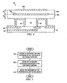
- FIGURE 1 shows one embodiment of a low profile antenna 10.
- the low profile antenna 10 generally comprises a balanced transmission line 12 having an interconnecting end 14, and a terminating end 16, electronic circuitry 18 coupled to the interconnecting end 14, and a parasitic element 26 disposed a predetermined distance from the terminating end 16.
- the balanced transmission line 12 may be made of any electrically conducting material and has a channel defining a central axis 22.
- the electronic circuitry 18 may be operable to manipulate electro-magnetic energy that is directed from the interconnecting end 14 to the terminating end 16 of the balanced transmission line 12 along the direction of the central axis 22.
- the electrical component of the electro-magnetic energy has a direction of polarization that may be generally perpendicular to the balanced transmission line 12 and to the electro-magnetic energy's direction of propagation.
- the electronic circuitry 18 may include any electrical component that is adapted to convert electro-magnetic energy suitable for use by the low profile antenna 10.
- the parasitic element 26 may be a flat plate made of a conducting material such as metal.
- the parasitic element 26 has a surface 28 that is generally perpendicular to the central axis such and covers an opening formed by the terminating end.
- the low profile antenna 10 may include a dielectric layer 30 that is disposed in between the terminating end 16 of the balanced transmission line 12 and surface 28 of the parasitic element 26.
- the balanced transmission line 12 may be a slotline, twinline, parallel plate, or other type of balanced structure.
- the transmission line 12 has a length that is significantly shorter than the wavelength ( ⁇ ) of the desired frequency of operation.
- the length of the transmission line 12 is the distance from the interconnecting 14 to the terminating 16 end.
- the length of the transmission line may be less than 1/4 wavelength of the operating frequency of the low profile antenna 10.
- the length of the transmission line may be as low as approximately 1/10 the operating frequency of the low profile antenna 10.
- a low profile antenna 10 may be constructed having a relatively low profile compared to known antenna designs with similar functionality. Therefore, tuning of the low profile antenna 10 is not accomplished by the transmission line 12; rather, tuning of the antenna is accomplished using the one or more parasitic elements 26 as will be described in detail below.
- Certain embodiments may provide coupling of the terminating end 16 of a balanced transmission line 12 to free space using the parasitic element 26.
- the parasitic element 26 may be operable to match the impedance (Z) of the balanced transmission line 12 to free space. It is known that relatively efficient coupling of an antenna to free space occurs when the output impedance of the antenna is approximately 377 ohms, the characteristic impedance of free space.
- particular physical characteristics of the parasitic element 26 or dielectric layer 30 may be selected in order to manipulate the output impedance of the low profile antenna 10.
- a width W of the parasitic element 26 may be selected in order to manipulate the output impedance of the low profile antenna 10.
- the dielectric layer 30 may be selected to have a predetermined depth D 1 . In this manner, the parasitic element 26 may be disposed a predetermined distance from the terminating end 16 that is essentially equal to depth D 1 .
- the dielectric layer 30 may be made of a material having a predetermined dielectric constant selected to manipulate the output impedance of the low profile antenna 10.
- the dielectric layer 30 may be an open gap such that the dielectric layer 30 is made of air. Given the insulative aspects of the dielectric layer 30, the parasitic element 26 has no direct coupling to the electronic circuitry 18 through the transmission line 12. Thus, the dielectric layer 30 may serve a dual purpose of providing structural support for the parasitic element 26 relative to the transmission line 12 as well as to provide another approach of manipulating the output impedance of the low profile antenna 10.
- the parasitic element 26 is shown centrally disposed over the transmission line 12; however, this is not necessary. In fact, the parasitic element 26 may be offset relative to the transmission line 12 in order to further manipulate various operating parameters of the low profile antenna 10.
- offset is referred to as placement of the parasitic element 26 over the transmission line 12 in such a manner that the transmission line 12 does not lie proximate the central portion of the parasitic element 26.
- the parasitic element 26 may be disposed in any manner such that the parasitic element 26 lies over the opening formed by the terminating end 16 of the balanced transmission line 12.
- FIGURE 2 depicts another embodiment of a low profile antenna 40 in which a number of balanced transmission lines 54 and parasitic elements 48 may be configured to transmit or receive electro-magnetic energy.
- Each transmission line 54 and parasitic element 48 functions in a similar manner to the transmission line 12 and parasitic element 26 respectively of FIGURE 1 .
- the embodiment of FIGURE 2 differs in that multiple transmission lines 54 and associated parasitic elements 48 may be used in order to form an array.
- the low profile antenna 40 may be referred to as an array because multiple transmission lines 54 are associated with a corresponding multiple parasitic elements 48.
- the low profile antenna 40 generally comprises a manifold board 42, a plurality of metallic frames 44, one or more dielectric layers 46, and one or more parasitic elements 48.
- the metallic frames 44 may be configured to serve as one or more baluns as well as one or more transmission lines 54 (to be described below).
- the manifold board 42 may include circuitry that may be operable to convey an electrical signal from an unbalanced line to each of the one or more U-shaped members 56 functioning as baluns.
- the unbalanced signal may be provided by any typical unbalanced transmission line (not specifically shown) that may be, for example, a coaxial cable, unbalanced t-line feed, stripline, or a microstrip.
- the low profile antenna 10 has a depth profile D 2 that is relatively short as compared with other known antenna designs.
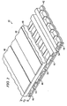
- FIGURE 3 shows one metallic frame 44 that has been removed from the low profile antenna 40.
- the metallic frame 44 has two inverted U-shaped members 56 and 58 that are interconnected by a cross member 62.
- One or more optional ribs 64 may be included to provide structural rigidity to the dielectric layer 46.
- the plurality of metallic frames 44 may be combined in such a manner to form the one or more transmission lines 54.
- FIGURE 4 is a partial elevational view of the embodiment of FIGURE 2 .
- a balanced transmission line 54 may be formed by adjacently disposed U-shaped members 56 and 58.
- U-shaped member 56 forms a folded balun that is operable to convert an unbalanced signal comprising electro-magnetic energy to a balanced signal suitable for use by the balanced transmission line 54.
- the U-shaped member 56 is connected to a feed line 64 that may be in turn, connected to an unbalanced line such as a coaxial cable, unbalanced t-line feed, stripline, or a microstrip feed line (not specifically shown).
- U-shaped member 58 may be connected to a ground plane 66.
- the balun which is formed by U-shaped member 56, feed line 64, and ground plane 66 may form a portion of an electronic circuit that is operable to provide a balanced signal comprising electro-magnetic energy to the balanced transmission line 54.
- two parasitic elements 48a and 48b are disposed over each of the U-shaped members 56 and 58.
- the low profile antenna 40 may have multiple parasitic elements 48a and 48b that serve to couple electro-magnetic energy from the transmission line 54 to free space. Neither of the parasitic elements 48a and 48b have any direct coupling to the transmission line 54 or to each other. Isolation of the parasitic elements 48a and 48b is accomplished by two associated dielectric layers 46a and 46b.
- Dielectric layer 46a serves to separate parasitic element 48a from the balanced transmission line 54 by a predetermined distance D 3 .
- the second dielectric layer 46b serves to separate parasitic element 48b from parasitic element 48b by a second predetermined distance D 4 .
- the dimensional qualities of parasitic element 48a and dielectric layer 46a may be selected in order to manipulate the output impedance of the low profile antenna 40. Additionally, the dimensional qualities of the second parasitic element 48b and second dielectric layer 46b may also be selected to further manipulate the output impedance of the low profile antenna 40. Although embodiments are described herein in which a quantity of two parasitic elements 48a and 48b are shown, it should be appreciated that any number of parasitic elements 48 may be used.
- FIGURE 5 shows a series of actions that may be performed in order to construct the low profile antenna 10 or 40.
- a low profile antenna 10 or 40 may be provided according to the embodiments of FIGURE 1 or FIGURES 2 through 4 respectively.
- the desired operating parameters of the low profile antenna 10 or 40 may be established.
- the desired operating parameters of the low profile antenna 10 or 40 may include a frequency of operation, a frequency bandwidth (BW), and a two-dimensional scan capability. For example, it may be desirable to construct a low profile antenna having an operating frequency of 12 Giga-Hertz at an operating bandwidth of 3:1 and a two-dimensional scan capability of 45 degrees.
- BW frequency bandwidth
- These desired operating parameters describe only one example of a low profile antenna 10 or 40 that may be constructed. It should be appreciated that a low profile having operating and physical parameters other than those described above may be constructed according to the
- the impedance of the transmission line 12 or 54 is generally matched to free space over the desired bandwidth of frequencies in act 104. It should be appreciated that the act of matching the transmission line 12 or 54 to free space is not intended to provide a perfect match over the entire range of desired operating bandwidth. However, the terminology "matched" is intended to indicate a level of impedance matching over the desired range of operating frequencies sufficient to allow transmission and/or reception of electro-magnetic energy from free space to the low profile antenna 10 or 40. The act of matching the transmission line 12 or 54 to free space may be accomplished by selecting one or more physical characteristics of the low profile antenna 10 or 40.
- the physical characteristics may include selecting the width of each of the one or more parasitic element 26 or 48, selecting a depth of the dielectric layer 30 or 46, selecting a dielectric constant of the material from which the dielectric layer 30 or 46 is formed, the number of parasitic elements 26 or 48 used, or the level of offset of the parasitic element 26 or 48 relative to the transmission line 12 or 54. It should be understood that other physical characteristics than those disclosed may be operable to modify the operating parameters of the low profile antenna 10 or 40. However, only several key physical characteristics have been disclosed for the purposes of brevity and clarity of disclosure.
- the low profile antenna 40 may be designed having a frequency of operation in the range of 6 to 18 Giga-Hertz having a frequency bandwidth of 3:1. Additionally, the low profile antenna 40 may have an overall depth D 2 of approximately 1/10 wavelength at the lowest operating frequency. The given operating parameters described above may be accomplished by implementing a quantity of two parasitic elements 48. Thus, it may be seen that a low profile antenna 40 may be realized having a relatively wide bandwidth in conjunction with a relatively low depth profile.
Abstract
Description
- This disclosure generally relates to antennas, and more particularly, to a low profile antenna and a method of constructing the same.
- An antenna is a type of device that is adapted to transmit and/or receive electro-magnetic energy. For electro-magnetic energy in the microwave frequencies, numerous differing types of antenna structures have been developed. One particular type of microwave antenna is the microstrip or patch antenna. Characteristic aspects of the patch antenna may include its relatively narrow bandwidth and low physical depth profile. Another popular type of microwave antenna is the notch antenna of which the flared notch antenna and cross notch antenna are several variations of the same. The notch antenna possesses a characteristically broader bandwidth than the patch antenna, yet requires a depth profile that is at least approximately 1/4 wavelength at the lowest desired operating frequency.
- It is an object of the present invention to provide a method of constructing an antenna and an antenna having a relatively low depth profile while having a relatively wide bandwidth of operation. This object can be achieved by the features as defined in the independent claims. Further enhancements are characterized in the dependent claims.
- In one embodiment, a low profile antenna comprises a balanced transmission line, electronic circuitry, and a parasitic element. The electronic circuitry is coupled to an interconnecting end of the transmission line and operable to direct electro-magnetic energy through the transmission line to a terminating end. The parasitic element has a surface that is disposed at a predetermined distance from the terminating end and normal to the central axis such that the surface of the parasitic element covers an opening formed by the terminating end.
- In another embodiment, a method for constructing a low profile antenna comprises providing a low profile antenna, determining the desired operating parameters of the antenna, and matching the impedance of the transmission line to free space. The low profile antenna generally includes a balanced transmission line, electronic circuitry, and a parasitic element. The electronic circuitry is coupled to an interconnecting end of the transmission line and operable to direct electro-magnetic energy through the transmission line to a terminating end. The parasitic element has a surface that is disposed at a predetermined distance from the terminating end and normal to the central axis such that the surface covers an opening formed by the terminating end.
- Certain embodiments may provide numerous technical advantages. A technical advantage of one embodiment may provide an antenna having a relatively low depth profile while having a relatively wide bandwidth of operation. While other prior art implementations such as notch antennas have a relatively wide bandwidth, they require a profile that is generally at least a 1/4 wavelength at the lowest frequency of operation. Certain embodiments may provide an operating bandwidth that is comparable to and yet have a depth profile significantly less than notch antenna designs.
- Although specific advantages have been enumerated above, various embodiments may include all, some, or none of the enumerated advantages. Additionally, other technical advantages may become readily apparent to one of ordinary skill in the art after review of the following figures and description.
- A more complete understanding of embodiments of the disclosure will be apparent from the examples given by the detailed description taken in conjunction with the accompanying drawings in which:
-
FIGURE 1 is an illustration of one embodiment of a low profile antenna; -
FIGURE 2 is a perspective view of another embodiment of a low profile antenna; -
FIGURE 3 is a perspective view of a metallic frame that may be used in conjunction with the embodiment ofFIGURE 2 ; -
FIGURE 4 is a partial elevational view of the embodiment ofFIGURE 2 ; and -
FIGURE 5 is a flowchart depicting a series of acts that may be utilized to construct the low profile antenna according to the embodiments ofFIGURE 1 orFIGURE 2 . - Embodiments of the invention now will be described more fully below with reference to the accompanying drawings. Reference numerals used throughout this document refer to like elements in the drawings.
-
FIGURE 1 shows one embodiment of alow profile antenna 10. Thelow profile antenna 10 generally comprises a balanced transmission line 12 having an interconnectingend 14, and a terminatingend 16,electronic circuitry 18 coupled to the interconnectingend 14, and aparasitic element 26 disposed a predetermined distance from the terminatingend 16. The balanced transmission line 12 may be made of any electrically conducting material and has a channel defining acentral axis 22. Theelectronic circuitry 18 may be operable to manipulate electro-magnetic energy that is directed from the interconnectingend 14 to the terminatingend 16 of the balanced transmission line 12 along the direction of thecentral axis 22. The electrical component of the electro-magnetic energy has a direction of polarization that may be generally perpendicular to the balanced transmission line 12 and to the electro-magnetic energy's direction of propagation. Theelectronic circuitry 18 may include any electrical component that is adapted to convert electro-magnetic energy suitable for use by thelow profile antenna 10. - In one embodiment, the
parasitic element 26 may be a flat plate made of a conducting material such as metal. Theparasitic element 26 has asurface 28 that is generally perpendicular to the central axis such and covers an opening formed by the terminating end. In another embodiment, thelow profile antenna 10 may include adielectric layer 30 that is disposed in between the terminatingend 16 of the balanced transmission line 12 andsurface 28 of theparasitic element 26. - The balanced transmission line 12 may be a slotline, twinline, parallel plate, or other type of balanced structure. In one embodiment, the transmission line 12 has a length that is significantly shorter than the wavelength (λ) of the desired frequency of operation. The length of the transmission line 12 is the distance from the interconnecting 14 to the terminating 16 end. In another embodiment, the length of the transmission line may be less than 1/4 wavelength of the operating frequency of the
low profile antenna 10. In yet another embodiment, the length of the transmission line may be as low as approximately 1/10 the operating frequency of thelow profile antenna 10. In this manner, alow profile antenna 10 may be constructed having a relatively low profile compared to known antenna designs with similar functionality. Therefore, tuning of thelow profile antenna 10 is not accomplished by the transmission line 12; rather, tuning of the antenna is accomplished using the one or moreparasitic elements 26 as will be described in detail below. - Certain embodiments may provide coupling of the terminating
end 16 of a balanced transmission line 12 to free space using theparasitic element 26. Stated another way, theparasitic element 26 may be operable to match the impedance (Z) of the balanced transmission line 12 to free space. It is known that relatively efficient coupling of an antenna to free space occurs when the output impedance of the antenna is approximately 377 ohms, the characteristic impedance of free space. To accomplish this, particular physical characteristics of theparasitic element 26 ordielectric layer 30 may be selected in order to manipulate the output impedance of thelow profile antenna 10. In one embodiment, a width W of theparasitic element 26 may be selected in order to manipulate the output impedance of thelow profile antenna 10. In another embodiment, thedielectric layer 30 may be selected to have a predetermined depth D1. In this manner, theparasitic element 26 may be disposed a predetermined distance from the terminatingend 16 that is essentially equal to depth D1. - In another embodiment, the
dielectric layer 30 may be made of a material having a predetermined dielectric constant selected to manipulate the output impedance of thelow profile antenna 10. In yet another embodiment, thedielectric layer 30 may be an open gap such that thedielectric layer 30 is made of air. Given the insulative aspects of thedielectric layer 30, theparasitic element 26 has no direct coupling to theelectronic circuitry 18 through the transmission line 12. Thus, thedielectric layer 30 may serve a dual purpose of providing structural support for theparasitic element 26 relative to the transmission line 12 as well as to provide another approach of manipulating the output impedance of thelow profile antenna 10. - The
parasitic element 26 is shown centrally disposed over the transmission line 12; however, this is not necessary. In fact, theparasitic element 26 may be offset relative to the transmission line 12 in order to further manipulate various operating parameters of thelow profile antenna 10. The term "offset" is referred to as placement of theparasitic element 26 over the transmission line 12 in such a manner that the transmission line 12 does not lie proximate the central portion of theparasitic element 26. Thus, theparasitic element 26 may be disposed in any manner such that theparasitic element 26 lies over the opening formed by the terminatingend 16 of the balanced transmission line 12. -
FIGURE 2 depicts another embodiment of alow profile antenna 40 in which a number ofbalanced transmission lines 54 andparasitic elements 48 may be configured to transmit or receive electro-magnetic energy. Eachtransmission line 54 andparasitic element 48 functions in a similar manner to the transmission line 12 andparasitic element 26 respectively ofFIGURE 1 . However, the embodiment ofFIGURE 2 differs in thatmultiple transmission lines 54 and associatedparasitic elements 48 may be used in order to form an array. - The
low profile antenna 40 may be referred to as an array becausemultiple transmission lines 54 are associated with a corresponding multipleparasitic elements 48. Thelow profile antenna 40 generally comprises amanifold board 42, a plurality ofmetallic frames 44, one or moredielectric layers 46, and one or moreparasitic elements 48. The metallic frames 44 may be configured to serve as one or more baluns as well as one or more transmission lines 54 (to be described below). Themanifold board 42 may include circuitry that may be operable to convey an electrical signal from an unbalanced line to each of the one or moreU-shaped members 56 functioning as baluns. The unbalanced signal may be provided by any typical unbalanced transmission line (not specifically shown) that may be, for example, a coaxial cable, unbalanced t-line feed, stripline, or a microstrip. In one embodiment, thelow profile antenna 10 has a depth profile D2 that is relatively short as compared with other known antenna designs. -
FIGURE 3 shows onemetallic frame 44 that has been removed from thelow profile antenna 40. Themetallic frame 44 has two invertedU-shaped members cross member 62. One or moreoptional ribs 64 may be included to provide structural rigidity to thedielectric layer 46. As will be described below, the plurality ofmetallic frames 44 may be combined in such a manner to form the one ormore transmission lines 54. -
FIGURE 4 is a partial elevational view of the embodiment ofFIGURE 2 . As shown, abalanced transmission line 54 may be formed by adjacently disposedU-shaped members U-shaped member 56 forms a folded balun that is operable to convert an unbalanced signal comprising electro-magnetic energy to a balanced signal suitable for use by thebalanced transmission line 54. TheU-shaped member 56 is connected to afeed line 64 that may be in turn, connected to an unbalanced line such as a coaxial cable, unbalanced t-line feed, stripline, or a microstrip feed line (not specifically shown).U-shaped member 58 may be connected to aground plane 66. Thus, the balun, which is formed byU-shaped member 56,feed line 64, andground plane 66 may form a portion of an electronic circuit that is operable to provide a balanced signal comprising electro-magnetic energy to thebalanced transmission line 54. - In this particular embodiment, two
parasitic elements U-shaped members low profile antenna 40 may have multipleparasitic elements transmission line 54 to free space. Neither of theparasitic elements transmission line 54 or to each other. Isolation of theparasitic elements dielectric layers Dielectric layer 46a serves to separateparasitic element 48a from thebalanced transmission line 54 by a predetermined distance D3. Thesecond dielectric layer 46b serves to separateparasitic element 48b fromparasitic element 48b by a second predetermined distance D4. In a similar manner to thelow profile antenna 10 ofFIGURE 1 , the dimensional qualities ofparasitic element 48a anddielectric layer 46a may be selected in order to manipulate the output impedance of thelow profile antenna 40. Additionally, the dimensional qualities of the secondparasitic element 48b and seconddielectric layer 46b may also be selected to further manipulate the output impedance of thelow profile antenna 40. Although embodiments are described herein in which a quantity of twoparasitic elements parasitic elements 48 may be used. -
FIGURE 5 shows a series of actions that may be performed in order to construct thelow profile antenna act 100, alow profile antenna FIGURE 1 orFIGURES 2 through 4 respectively. Next inact 102, the desired operating parameters of thelow profile antenna low profile antenna low profile antenna - Once the desired operating parameters have been established, the impedance of the
transmission line 12 or 54 is generally matched to free space over the desired bandwidth of frequencies inact 104. It should be appreciated that the act of matching thetransmission line 12 or 54 to free space is not intended to provide a perfect match over the entire range of desired operating bandwidth. However, the terminology "matched" is intended to indicate a level of impedance matching over the desired range of operating frequencies sufficient to allow transmission and/or reception of electro-magnetic energy from free space to thelow profile antenna transmission line 12 or 54 to free space may be accomplished by selecting one or more physical characteristics of thelow profile antenna parasitic element dielectric layer dielectric layer parasitic elements parasitic element transmission line 12 or 54. It should be understood that other physical characteristics than those disclosed may be operable to modify the operating parameters of thelow profile antenna - Test results of an actual reduction to practice determine that the
low profile antenna 40 may be designed having a frequency of operation in the range of 6 to 18 Giga-Hertz having a frequency bandwidth of 3:1. Additionally, thelow profile antenna 40 may have an overall depth D2 of approximately 1/10 wavelength at the lowest operating frequency. The given operating parameters described above may be accomplished by implementing a quantity of twoparasitic elements 48. Thus, it may be seen that alow profile antenna 40 may be realized having a relatively wide bandwidth in conjunction with a relatively low depth profile. - Although the present invention has been described with several embodiments, a myriad of changes, variations, alterations, transformations, and modifications may be suggested to one skilled in the art, and it is intended that the present invention encompass such changes, variations, alterations, transformation, and modifications as they fall within the scope of the appended claims.
Claims (20)
- An antenna comprising:a balanced transmission line having an interconnecting end, a terminating end, and a channel defining a central axis;electronic circuitry coupled to the interconnecting end and operable to direct electro-magnetic energy towards the terminating end along a direction of propagation, the direction of propagation being essentially co-linear with the central axis; andat least one parasitic element having a surface that is disposed at a predetermined distance from the terminating end and normal to the central axis such that the surface covers an opening formed by the terminating end.
- The antenna of Claim 1, wherein the parasitic element is a generally flat plate.
- The antenna of Claim 1 or 2, wherein the electronic circuitry comprises a balun.
- The antenna of Claim 3, wherein the balun is a folded balun.
- The antenna according to any one of the preceding claims, wherein the electronic circuitry comprises a ground plane.
- The antenna according to any one of the preceding claims, wherein the balanced transmission line comprises a pair of parallel plates.
- The antenna of Claim 6, wherein each of the parallel plates forms a portion of a folded balun.
- The antenna according to any one of the preceding claims, wherein the antenna has an operating bandwidth of approximately 3:1.
- The antenna according to any one of the preceding claims, wherein the balanced transmission line is a slotline, twinline, or parallel plate.
- The antenna according to any one of the preceding claims, further comprises a dielectric layer disposed in between the terminating end of the balanced transmission line and the surface of the parasitic element.
- The antenna according to any one of the preceding claims, wherein the at least one parasitic element comprises at least two parasitic elements.
- The antenna according to any one of the preceding claims, wherein the transmission line has a length that is less than 1/4 of the wavelength of the operating frequency of the low profile antenna.
- An low profile antenna comprising:a pair of parallel plates defining a transmission line having an interconnecting end, a terminating end, and a channel defining a central axis, one of the parallel plates forming a portion of a folded balun and the other one of the parallel plates being coupled to a ground plane, the interconnecting end being coupled to an unbalanced transmission line;at least one generally flat plate having a surface that is disposed at a predetermined distance from the terminating end and normal to the central axis such that the surface covers an opening formed by the terminating end; anda dielectric layer disposed in between the terminating end of the balanced transmission line and the surface of the parasitic element.
- The antenna of Claim 13, wherein the at least one parasitic element comprises at least two parasitic elements.
- The antenna of Claim 13 or 14, wherein the transmission line has a length that is less than 1/4 of the wavelength of the operating frequency of the low profile antenna
- A method of constructing an antenna comprising:providing an antenna comprising a balanced transmission line having an interconnecting end, a terminating end, and a channel defining a central axis, electronic circuitry coupled to the interconnecting end and operable to direct electro-magnetic energy towards the terminating end along a direction of propagation, the direction of propagation being essentially co-linear with the central axis, and at least one parasitic element having a surface that is disposed at a predetermined distance from the terminating end and normal to the direction of propagation such that the surface covers an opening formed by the terminating end;determining the desired operating parameters of the antenna; andmatching the impedance of the transmission line to free space.
- The method of Claim 16, wherein matching the impedance of the transmission line to free space further comprises selecting a width of the at least one parasitic element.
- The method of Claim 16 or 17, wherein matching the impedance of the transmission line to free space further comprises selecting a depth of the dielectric layer.
- The method according to any one of the preceding claims 16 to 18, wherein matching the impedance of the transmission line to free space further comprises selecting a dielectric constant of the material from which the dielectric layer is formed.
- The method according to any one of the preceding claims 16 to 19, wherein matching the impedance of the transmission line to free space further comprises selecting a quantity of the at least one parasitic elements.
Applications Claiming Priority (1)
| Application Number | Priority Date | Filing Date | Title |
|---|---|---|---|
| US11/734,517 US7948441B2 (en) | 2007-04-12 | 2007-04-12 | Low profile antenna |
Publications (2)
| Publication Number | Publication Date |
|---|---|
| EP1981121A1 true EP1981121A1 (en) | 2008-10-15 |
| EP1981121B1 EP1981121B1 (en) | 2014-04-23 |
Family
ID=39495228
Family Applications (1)
| Application Number | Title | Priority Date | Filing Date |
|---|---|---|---|
| EP08006242.5A Active EP1981121B1 (en) | 2007-04-12 | 2008-03-31 | Low profile antenna |
Country Status (2)
| Country | Link |
|---|---|
| US (1) | US7948441B2 (en) |
| EP (1) | EP1981121B1 (en) |
Families Citing this family (15)
| Publication number | Priority date | Publication date | Assignee | Title |
|---|---|---|---|---|
| US9537208B2 (en) | 2012-11-12 | 2017-01-03 | Raytheon Company | Dual polarization current loop radiator with integrated balun |
| US10581177B2 (en) | 2016-12-15 | 2020-03-03 | Raytheon Company | High frequency polymer on metal radiator |
| US11088467B2 (en) | 2016-12-15 | 2021-08-10 | Raytheon Company | Printed wiring board with radiator and feed circuit |
| US10541461B2 (en) | 2016-12-16 | 2020-01-21 | Ratheon Company | Tile for an active electronically scanned array (AESA) |
| JP6597659B2 (en) * | 2017-02-01 | 2019-10-30 | 株式会社村田製作所 | ANTENNA DEVICE AND ANTENNA DEVICE MANUFACTURING METHOD |
| US10361485B2 (en) | 2017-08-04 | 2019-07-23 | Raytheon Company | Tripole current loop radiating element with integrated circularly polarized feed |
| US10971806B2 (en) | 2017-08-22 | 2021-04-06 | The Boeing Company | Broadband conformal antenna |
| US10826186B2 (en) | 2017-08-28 | 2020-11-03 | Raytheon Company | Surface mounted notch radiator with folded balun |
| US10424847B2 (en) | 2017-09-08 | 2019-09-24 | Raytheon Company | Wideband dual-polarized current loop antenna element |
| US11233310B2 (en) * | 2018-01-29 | 2022-01-25 | The Boeing Company | Low-profile conformal antenna |
| US10916853B2 (en) | 2018-08-24 | 2021-02-09 | The Boeing Company | Conformal antenna with enhanced circular polarization |
| US10938082B2 (en) | 2018-08-24 | 2021-03-02 | The Boeing Company | Aperture-coupled microstrip-to-waveguide transitions |
| US10923831B2 (en) | 2018-08-24 | 2021-02-16 | The Boeing Company | Waveguide-fed planar antenna array with enhanced circular polarization |
| US11276933B2 (en) | 2019-11-06 | 2022-03-15 | The Boeing Company | High-gain antenna with cavity between feed line and ground plane |
| US11152715B2 (en) | 2020-02-18 | 2021-10-19 | Raytheon Company | Dual differential radiator |
Citations (5)
| Publication number | Priority date | Publication date | Assignee | Title |
|---|---|---|---|---|
| US3976959A (en) * | 1974-07-22 | 1976-08-24 | Gaspari Russell A | Planar balun |
| EP0323664A2 (en) * | 1987-12-22 | 1989-07-12 | Philips Electronics Uk Limited | Coplanar patch antenna |
| US5594455A (en) * | 1994-06-13 | 1997-01-14 | Nippon Telegraph & Telephone Corporation | Bidirectional printed antenna |
| WO2001031735A1 (en) * | 1999-10-28 | 2001-05-03 | Qualcomm Incorporated | Balanced, retractable mobile phone antenna |
| US20050219008A1 (en) * | 2002-09-03 | 2005-10-06 | Broadcom Corporation | Compact balun with rejection filter for 802.11a and 802.11b simultaneous operation |
Family Cites Families (20)
| Publication number | Priority date | Publication date | Assignee | Title |
|---|---|---|---|---|
| US3740754A (en) | 1972-05-24 | 1973-06-19 | Gte Sylvania Inc | Broadband cup-dipole and cup-turnstile antennas |
| JPH0612852B2 (en) | 1986-03-18 | 1994-02-16 | 日本無線株式会社 | parabolic antenna |
| FR2654554B1 (en) * | 1989-11-10 | 1992-07-31 | France Etat | ANTENNA IN PROPELLER, QUADRIFILAIRE, RESONANT BICOUCHE. |
| WO1998003449A1 (en) | 1996-07-20 | 1998-01-29 | Dynamit Nobel Gmbh Explosivstoff- Und Systemtechnik | Pyrotechnic mixture as propellant or a gas charge with carbon monoxide-reduced vapors |
| US5874924A (en) | 1997-11-17 | 1999-02-23 | Lockheed Martin Corp. | Spacecraft antenna array with directivity enhancing rings |
| US6097349A (en) * | 1997-11-18 | 2000-08-01 | Ericsson Inc. | Compact antenna feed circuits |
| US6114997A (en) | 1998-05-27 | 2000-09-05 | Raytheon Company | Low-profile, integrated radiator tiles for wideband, dual-linear and circular-polarized phased array applications |
| US6147653A (en) * | 1998-12-07 | 2000-11-14 | Wallace; Raymond C. | Balanced dipole antenna for mobile phones |
| US6310585B1 (en) * | 1999-09-29 | 2001-10-30 | Radio Frequency Systems, Inc. | Isolation improvement mechanism for dual polarization scanning antennas |
| US6300906B1 (en) | 2000-01-05 | 2001-10-09 | Harris Corporation | Wideband phased array antenna employing increased packaging density laminate structure containing feed network, balun and power divider circuitry |
| US6747606B2 (en) | 2002-05-31 | 2004-06-08 | Radio Frequency Systems Inc. | Single or dual polarized molded dipole antenna having integrated feed structure |
| US6924776B2 (en) * | 2003-07-03 | 2005-08-02 | Andrew Corporation | Wideband dual polarized base station antenna offering optimized horizontal beam radiation patterns and variable vertical beam tilt |
| US7283101B2 (en) | 2003-06-26 | 2007-10-16 | Andrew Corporation | Antenna element, feed probe; dielectric spacer, antenna and method of communicating with a plurality of devices |
| DE202004008770U1 (en) | 2004-06-03 | 2004-08-12 | Kathrein-Werke Kg | Mobile radio base station antenna element has conducting main reflector, dual polarized radiator and cross shaped passive subreflector |
| US7068235B2 (en) | 2004-07-26 | 2006-06-27 | Row 44, Llc | Antenna system |
| JP4408405B2 (en) * | 2004-09-21 | 2010-02-03 | 富士通株式会社 | Planar antenna and radio equipment |
| GB2424765B (en) | 2005-03-29 | 2007-07-25 | Csa Ltd | A dipole antenna |
| WO2006114455A1 (en) | 2005-04-25 | 2006-11-02 | Radiacion Y Microondas, S.A. | Cavity antenna that is excited with one or more dipoles |
| US7388556B2 (en) | 2005-06-01 | 2008-06-17 | Andrew Corporation | Antenna providing downtilt and preserving half power beam width |
| US7688265B2 (en) | 2007-09-18 | 2010-03-30 | Raytheon Company | Dual polarized low profile antenna |
-
2007
- 2007-04-12 US US11/734,517 patent/US7948441B2/en active Active
-
2008
- 2008-03-31 EP EP08006242.5A patent/EP1981121B1/en active Active
Patent Citations (5)
| Publication number | Priority date | Publication date | Assignee | Title |
|---|---|---|---|---|
| US3976959A (en) * | 1974-07-22 | 1976-08-24 | Gaspari Russell A | Planar balun |
| EP0323664A2 (en) * | 1987-12-22 | 1989-07-12 | Philips Electronics Uk Limited | Coplanar patch antenna |
| US5594455A (en) * | 1994-06-13 | 1997-01-14 | Nippon Telegraph & Telephone Corporation | Bidirectional printed antenna |
| WO2001031735A1 (en) * | 1999-10-28 | 2001-05-03 | Qualcomm Incorporated | Balanced, retractable mobile phone antenna |
| US20050219008A1 (en) * | 2002-09-03 | 2005-10-06 | Broadcom Corporation | Compact balun with rejection filter for 802.11a and 802.11b simultaneous operation |
Non-Patent Citations (4)
| Title |
|---|
| "IEEE Transactions on Microwave Theory and Techniques", vol. 44, 1 December 1996, article "Oscillator-Type Active-Integrated Antenna: The Leaky-Mode Approach", pages: 2265 - 2272 |
| "IEEE", vol. 4, 4 December 2005, I-JEN CHEN, article "CPW-Fed Circularly Polarized 2x2 Sequentially Rotated Patch Antenna Array", pages: 1 - 3 |
| CHEN I-J: "CPW-Fed Circularly Polarized 2*2 Sequentially Rotated Patch Antenna Array", MICROWAVE CONFERENCE PROCEEDINGS, 2005. APMC 2005. ASIA-PACIFIC CONFER ENCE PROCEEDINGS SUZHOU, CHINA 04-07 DEC. 2005, PISCATAWAY, NJ, USA,IEEE, vol. 4, 4 December 2005 (2005-12-04), pages 1 - 3, XP010902322, ISBN: 978-0-7803-9433-9 * |
| GUANG-JONG CHOU ET AL: "Oscillator-Type Active-Integrated Antenna: The Leaky-Mode Approach", 19961201, vol. 44, no. 12, 1 December 1996 (1996-12-01), XP011036631 * |
Also Published As
| Publication number | Publication date |
|---|---|
| US7948441B2 (en) | 2011-05-24 |
| US20080252544A1 (en) | 2008-10-16 |
| EP1981121B1 (en) | 2014-04-23 |
Similar Documents
| Publication | Publication Date | Title |
|---|---|---|
| US7948441B2 (en) | Low profile antenna | |
| CN111525252B (en) | Broadband dual-polarized antenna unit based on coupling feed | |
| JP6820135B2 (en) | Ultra-wideband antenna elements and arrays with low cross-polarization decade bandwidth | |
| US7642979B2 (en) | Wave-guide-notch antenna | |
| US6292153B1 (en) | Antenna comprising two wideband notch regions on one coplanar substrate | |
| US9653810B2 (en) | Waveguide fed and wideband complementary antenna | |
| US6246377B1 (en) | Antenna comprising two separate wideband notch regions on one coplanar substrate | |
| US7180457B2 (en) | Wideband phased array radiator | |
| CN106252872B (en) | Co-polarized microstrip duplex antenna array | |
| US7688265B2 (en) | Dual polarized low profile antenna | |
| US20040104859A1 (en) | Wide bandwidth flat panel antenna array | |
| CN101662073A (en) | Horn antenna with integrated impedance matching network for improved operating frequency range | |
| US20090033559A1 (en) | Broadband antenna system | |
| US20060038732A1 (en) | Broadband dual polarized slotline feed circuit | |
| CN104377449A (en) | Broadband microstrip antenna and antenna array | |
| US20210273339A1 (en) | Wideband Dual-Polarized Four-Quad Loop Antenna | |
| EP2351149A1 (en) | Wideband radiating elements | |
| CN205621858U (en) | Two circular polarization microstrip antenna of miniaturized low section broadband | |
| KR101496302B1 (en) | Millimeter Wave Transition Method Between Microstrip Line and Waveguide | |
| US8008997B2 (en) | Printed circuit board filter having rows of vias defining a quasi cavity that is below a cutoff frequency | |
| Bah et al. | An extremely wideband tapered balun for application in tightly coupled arrays | |
| CN206076497U (en) | Same polarization micro-strip duplexed antenna array | |
| US20160308284A1 (en) | Balun | |
| CN109509964A (en) | A kind of broadband circle polarized array antenna | |
| JPS6243906A (en) | Microstrip antenna |
Legal Events
| Date | Code | Title | Description |
|---|---|---|---|
| PUAI | Public reference made under article 153(3) epc to a published international application that has entered the european phase |
Free format text: ORIGINAL CODE: 0009012 |
|
| 17P | Request for examination filed |
Effective date: 20080331 |
|
| AK | Designated contracting states |
Kind code of ref document: A1 Designated state(s): AT BE BG CH CY CZ DE DK EE ES FI FR GB GR HR HU IE IS IT LI LT LU LV MC MT NL NO PL PT RO SE SI SK TR |
|
| AX | Request for extension of the european patent |
Extension state: AL BA MK RS |
|
| 17Q | First examination report despatched |
Effective date: 20090421 |
|
| AKX | Designation fees paid |
Designated state(s): AT BE BG CH CY CZ DE DK EE ES FI FR GB GR HR HU IE IS IT LI LT LU LV MC MT NL NO PL PT RO SE SI SK TR |
|
| GRAP | Despatch of communication of intention to grant a patent |
Free format text: ORIGINAL CODE: EPIDOSNIGR1 |
|
| INTG | Intention to grant announced |
Effective date: 20131128 |
|
| GRAS | Grant fee paid |
Free format text: ORIGINAL CODE: EPIDOSNIGR3 |
|
| GRAA | (expected) grant |
Free format text: ORIGINAL CODE: 0009210 |
|
| AK | Designated contracting states |
Kind code of ref document: B1 Designated state(s): AT BE BG CH CY CZ DE DK EE ES FI FR GB GR HR HU IE IS IT LI LT LU LV MC MT NL NO PL PT RO SE SI SK TR |
|
| REG | Reference to a national code |
Ref country code: GB Ref legal event code: FG4D |
|
| REG | Reference to a national code |
Ref country code: CH Ref legal event code: EP |
|
| REG | Reference to a national code |
Ref country code: AT Ref legal event code: REF Ref document number: 664312 Country of ref document: AT Kind code of ref document: T Effective date: 20140515 |
|
| REG | Reference to a national code |
Ref country code: IE Ref legal event code: FG4D |
|
| REG | Reference to a national code |
Ref country code: DE Ref legal event code: R096 Ref document number: 602008031644 Country of ref document: DE Effective date: 20140605 |
|
| REG | Reference to a national code |
Ref country code: AT Ref legal event code: MK05 Ref document number: 664312 Country of ref document: AT Kind code of ref document: T Effective date: 20140423 |
|
| REG | Reference to a national code |
Ref country code: NL Ref legal event code: VDEP Effective date: 20140423 |
|
| REG | Reference to a national code |
Ref country code: LT Ref legal event code: MG4D |
|
| PG25 | Lapsed in a contracting state [announced via postgrant information from national office to epo] |
Ref country code: FI Free format text: LAPSE BECAUSE OF FAILURE TO SUBMIT A TRANSLATION OF THE DESCRIPTION OR TO PAY THE FEE WITHIN THE PRESCRIBED TIME-LIMIT Effective date: 20140423 Ref country code: CY Free format text: LAPSE BECAUSE OF FAILURE TO SUBMIT A TRANSLATION OF THE DESCRIPTION OR TO PAY THE FEE WITHIN THE PRESCRIBED TIME-LIMIT Effective date: 20140423 Ref country code: IS Free format text: LAPSE BECAUSE OF FAILURE TO SUBMIT A TRANSLATION OF THE DESCRIPTION OR TO PAY THE FEE WITHIN THE PRESCRIBED TIME-LIMIT Effective date: 20140823 Ref country code: NO Free format text: LAPSE BECAUSE OF FAILURE TO SUBMIT A TRANSLATION OF THE DESCRIPTION OR TO PAY THE FEE WITHIN THE PRESCRIBED TIME-LIMIT Effective date: 20140723 Ref country code: GR Free format text: LAPSE BECAUSE OF FAILURE TO SUBMIT A TRANSLATION OF THE DESCRIPTION OR TO PAY THE FEE WITHIN THE PRESCRIBED TIME-LIMIT Effective date: 20140724 Ref country code: BG Free format text: LAPSE BECAUSE OF FAILURE TO SUBMIT A TRANSLATION OF THE DESCRIPTION OR TO PAY THE FEE WITHIN THE PRESCRIBED TIME-LIMIT Effective date: 20140723 Ref country code: NL Free format text: LAPSE BECAUSE OF FAILURE TO SUBMIT A TRANSLATION OF THE DESCRIPTION OR TO PAY THE FEE WITHIN THE PRESCRIBED TIME-LIMIT Effective date: 20140423 Ref country code: LT Free format text: LAPSE BECAUSE OF FAILURE TO SUBMIT A TRANSLATION OF THE DESCRIPTION OR TO PAY THE FEE WITHIN THE PRESCRIBED TIME-LIMIT Effective date: 20140423 |
|
| PG25 | Lapsed in a contracting state [announced via postgrant information from national office to epo] |
Ref country code: SE Free format text: LAPSE BECAUSE OF FAILURE TO SUBMIT A TRANSLATION OF THE DESCRIPTION OR TO PAY THE FEE WITHIN THE PRESCRIBED TIME-LIMIT Effective date: 20140423 Ref country code: LV Free format text: LAPSE BECAUSE OF FAILURE TO SUBMIT A TRANSLATION OF THE DESCRIPTION OR TO PAY THE FEE WITHIN THE PRESCRIBED TIME-LIMIT Effective date: 20140423 Ref country code: ES Free format text: LAPSE BECAUSE OF FAILURE TO SUBMIT A TRANSLATION OF THE DESCRIPTION OR TO PAY THE FEE WITHIN THE PRESCRIBED TIME-LIMIT Effective date: 20140423 Ref country code: PL Free format text: LAPSE BECAUSE OF FAILURE TO SUBMIT A TRANSLATION OF THE DESCRIPTION OR TO PAY THE FEE WITHIN THE PRESCRIBED TIME-LIMIT Effective date: 20140423 Ref country code: HR Free format text: LAPSE BECAUSE OF FAILURE TO SUBMIT A TRANSLATION OF THE DESCRIPTION OR TO PAY THE FEE WITHIN THE PRESCRIBED TIME-LIMIT Effective date: 20140423 Ref country code: AT Free format text: LAPSE BECAUSE OF FAILURE TO SUBMIT A TRANSLATION OF THE DESCRIPTION OR TO PAY THE FEE WITHIN THE PRESCRIBED TIME-LIMIT Effective date: 20140423 |
|
| PG25 | Lapsed in a contracting state [announced via postgrant information from national office to epo] |
Ref country code: PT Free format text: LAPSE BECAUSE OF FAILURE TO SUBMIT A TRANSLATION OF THE DESCRIPTION OR TO PAY THE FEE WITHIN THE PRESCRIBED TIME-LIMIT Effective date: 20140825 |
|
| REG | Reference to a national code |
Ref country code: DE Ref legal event code: R097 Ref document number: 602008031644 Country of ref document: DE |
|
| PG25 | Lapsed in a contracting state [announced via postgrant information from national office to epo] |
Ref country code: SK Free format text: LAPSE BECAUSE OF FAILURE TO SUBMIT A TRANSLATION OF THE DESCRIPTION OR TO PAY THE FEE WITHIN THE PRESCRIBED TIME-LIMIT Effective date: 20140423 Ref country code: RO Free format text: LAPSE BECAUSE OF FAILURE TO SUBMIT A TRANSLATION OF THE DESCRIPTION OR TO PAY THE FEE WITHIN THE PRESCRIBED TIME-LIMIT Effective date: 20140423 Ref country code: CZ Free format text: LAPSE BECAUSE OF FAILURE TO SUBMIT A TRANSLATION OF THE DESCRIPTION OR TO PAY THE FEE WITHIN THE PRESCRIBED TIME-LIMIT Effective date: 20140423 Ref country code: DK Free format text: LAPSE BECAUSE OF FAILURE TO SUBMIT A TRANSLATION OF THE DESCRIPTION OR TO PAY THE FEE WITHIN THE PRESCRIBED TIME-LIMIT Effective date: 20140423 Ref country code: BE Free format text: LAPSE BECAUSE OF FAILURE TO SUBMIT A TRANSLATION OF THE DESCRIPTION OR TO PAY THE FEE WITHIN THE PRESCRIBED TIME-LIMIT Effective date: 20140423 Ref country code: EE Free format text: LAPSE BECAUSE OF FAILURE TO SUBMIT A TRANSLATION OF THE DESCRIPTION OR TO PAY THE FEE WITHIN THE PRESCRIBED TIME-LIMIT Effective date: 20140423 |
|
| PLBE | No opposition filed within time limit |
Free format text: ORIGINAL CODE: 0009261 |
|
| STAA | Information on the status of an ep patent application or granted ep patent |
Free format text: STATUS: NO OPPOSITION FILED WITHIN TIME LIMIT |
|
| PG25 | Lapsed in a contracting state [announced via postgrant information from national office to epo] |
Ref country code: IT Free format text: LAPSE BECAUSE OF FAILURE TO SUBMIT A TRANSLATION OF THE DESCRIPTION OR TO PAY THE FEE WITHIN THE PRESCRIBED TIME-LIMIT Effective date: 20140423 |
|
| 26N | No opposition filed |
Effective date: 20150126 |
|
| REG | Reference to a national code |
Ref country code: DE Ref legal event code: R097 Ref document number: 602008031644 Country of ref document: DE Effective date: 20150126 |
|
| PG25 | Lapsed in a contracting state [announced via postgrant information from national office to epo] |
Ref country code: SI Free format text: LAPSE BECAUSE OF FAILURE TO SUBMIT A TRANSLATION OF THE DESCRIPTION OR TO PAY THE FEE WITHIN THE PRESCRIBED TIME-LIMIT Effective date: 20140423 |
|
| PG25 | Lapsed in a contracting state [announced via postgrant information from national office to epo] |
Ref country code: MC Free format text: LAPSE BECAUSE OF FAILURE TO SUBMIT A TRANSLATION OF THE DESCRIPTION OR TO PAY THE FEE WITHIN THE PRESCRIBED TIME-LIMIT Effective date: 20140423 Ref country code: LU Free format text: LAPSE BECAUSE OF FAILURE TO SUBMIT A TRANSLATION OF THE DESCRIPTION OR TO PAY THE FEE WITHIN THE PRESCRIBED TIME-LIMIT Effective date: 20150331 |
|
| REG | Reference to a national code |
Ref country code: CH Ref legal event code: PL |
|
| REG | Reference to a national code |
Ref country code: IE Ref legal event code: MM4A |
|
| PG25 | Lapsed in a contracting state [announced via postgrant information from national office to epo] |
Ref country code: LI Free format text: LAPSE BECAUSE OF NON-PAYMENT OF DUE FEES Effective date: 20150331 Ref country code: IE Free format text: LAPSE BECAUSE OF NON-PAYMENT OF DUE FEES Effective date: 20150331 Ref country code: CH Free format text: LAPSE BECAUSE OF NON-PAYMENT OF DUE FEES Effective date: 20150331 |
|
| REG | Reference to a national code |
Ref country code: FR Ref legal event code: PLFP Year of fee payment: 9 |
|
| PG25 | Lapsed in a contracting state [announced via postgrant information from national office to epo] |
Ref country code: MT Free format text: LAPSE BECAUSE OF FAILURE TO SUBMIT A TRANSLATION OF THE DESCRIPTION OR TO PAY THE FEE WITHIN THE PRESCRIBED TIME-LIMIT Effective date: 20140423 |
|
| REG | Reference to a national code |
Ref country code: FR Ref legal event code: PLFP Year of fee payment: 10 |
|
| PG25 | Lapsed in a contracting state [announced via postgrant information from national office to epo] |
Ref country code: HU Free format text: LAPSE BECAUSE OF FAILURE TO SUBMIT A TRANSLATION OF THE DESCRIPTION OR TO PAY THE FEE WITHIN THE PRESCRIBED TIME-LIMIT; INVALID AB INITIO Effective date: 20080331 |
|
| PG25 | Lapsed in a contracting state [announced via postgrant information from national office to epo] |
Ref country code: TR Free format text: LAPSE BECAUSE OF FAILURE TO SUBMIT A TRANSLATION OF THE DESCRIPTION OR TO PAY THE FEE WITHIN THE PRESCRIBED TIME-LIMIT Effective date: 20140423 |
|
| REG | Reference to a national code |
Ref country code: FR Ref legal event code: PLFP Year of fee payment: 11 |
|
| PGFP | Annual fee paid to national office [announced via postgrant information from national office to epo] |
Ref country code: FR Payment date: 20230222 Year of fee payment: 16 |
|
| PGFP | Annual fee paid to national office [announced via postgrant information from national office to epo] |
Ref country code: GB Payment date: 20230221 Year of fee payment: 16 Ref country code: DE Payment date: 20230221 Year of fee payment: 16 |
|
| P01 | Opt-out of the competence of the unified patent court (upc) registered |
Effective date: 20230530 |