EP2009714A2 - Method and device for separating in particular metered layers by means of OVPD or similar - Google Patents
Method and device for separating in particular metered layers by means of OVPD or similar Download PDFInfo
- Publication number
- EP2009714A2 EP2009714A2 EP08159270A EP08159270A EP2009714A2 EP 2009714 A2 EP2009714 A2 EP 2009714A2 EP 08159270 A EP08159270 A EP 08159270A EP 08159270 A EP08159270 A EP 08159270A EP 2009714 A2 EP2009714 A2 EP 2009714A2
- Authority
- EP
- European Patent Office
- Prior art keywords
- modification
- starting material
- dopant
- chamber
- plasma
- Prior art date
- Legal status (The legal status is an assumption and is not a legal conclusion. Google has not performed a legal analysis and makes no representation as to the accuracy of the status listed.)
- Granted
Links
Images
Classifications
-
- B—PERFORMING OPERATIONS; TRANSPORTING
- B82—NANOTECHNOLOGY
- B82Y—SPECIFIC USES OR APPLICATIONS OF NANOSTRUCTURES; MEASUREMENT OR ANALYSIS OF NANOSTRUCTURES; MANUFACTURE OR TREATMENT OF NANOSTRUCTURES
- B82Y10/00—Nanotechnology for information processing, storage or transmission, e.g. quantum computing or single electron logic
-
- C—CHEMISTRY; METALLURGY
- C23—COATING METALLIC MATERIAL; COATING MATERIAL WITH METALLIC MATERIAL; CHEMICAL SURFACE TREATMENT; DIFFUSION TREATMENT OF METALLIC MATERIAL; COATING BY VACUUM EVAPORATION, BY SPUTTERING, BY ION IMPLANTATION OR BY CHEMICAL VAPOUR DEPOSITION, IN GENERAL; INHIBITING CORROSION OF METALLIC MATERIAL OR INCRUSTATION IN GENERAL
- C23C—COATING METALLIC MATERIAL; COATING MATERIAL WITH METALLIC MATERIAL; SURFACE TREATMENT OF METALLIC MATERIAL BY DIFFUSION INTO THE SURFACE, BY CHEMICAL CONVERSION OR SUBSTITUTION; COATING BY VACUUM EVAPORATION, BY SPUTTERING, BY ION IMPLANTATION OR BY CHEMICAL VAPOUR DEPOSITION, IN GENERAL
- C23C14/00—Coating by vacuum evaporation, by sputtering or by ion implantation of the coating forming material
- C23C14/06—Coating by vacuum evaporation, by sputtering or by ion implantation of the coating forming material characterised by the coating material
- C23C14/12—Organic material
-
- C—CHEMISTRY; METALLURGY
- C23—COATING METALLIC MATERIAL; COATING MATERIAL WITH METALLIC MATERIAL; CHEMICAL SURFACE TREATMENT; DIFFUSION TREATMENT OF METALLIC MATERIAL; COATING BY VACUUM EVAPORATION, BY SPUTTERING, BY ION IMPLANTATION OR BY CHEMICAL VAPOUR DEPOSITION, IN GENERAL; INHIBITING CORROSION OF METALLIC MATERIAL OR INCRUSTATION IN GENERAL
- C23C—COATING METALLIC MATERIAL; COATING MATERIAL WITH METALLIC MATERIAL; SURFACE TREATMENT OF METALLIC MATERIAL BY DIFFUSION INTO THE SURFACE, BY CHEMICAL CONVERSION OR SUBSTITUTION; COATING BY VACUUM EVAPORATION, BY SPUTTERING, BY ION IMPLANTATION OR BY CHEMICAL VAPOUR DEPOSITION, IN GENERAL
- C23C14/00—Coating by vacuum evaporation, by sputtering or by ion implantation of the coating forming material
- C23C14/22—Coating by vacuum evaporation, by sputtering or by ion implantation of the coating forming material characterised by the process of coating
- C23C14/228—Gas flow assisted PVD deposition
-
- C—CHEMISTRY; METALLURGY
- C23—COATING METALLIC MATERIAL; COATING MATERIAL WITH METALLIC MATERIAL; CHEMICAL SURFACE TREATMENT; DIFFUSION TREATMENT OF METALLIC MATERIAL; COATING BY VACUUM EVAPORATION, BY SPUTTERING, BY ION IMPLANTATION OR BY CHEMICAL VAPOUR DEPOSITION, IN GENERAL; INHIBITING CORROSION OF METALLIC MATERIAL OR INCRUSTATION IN GENERAL
- C23C—COATING METALLIC MATERIAL; COATING MATERIAL WITH METALLIC MATERIAL; SURFACE TREATMENT OF METALLIC MATERIAL BY DIFFUSION INTO THE SURFACE, BY CHEMICAL CONVERSION OR SUBSTITUTION; COATING BY VACUUM EVAPORATION, BY SPUTTERING, BY ION IMPLANTATION OR BY CHEMICAL VAPOUR DEPOSITION, IN GENERAL
- C23C14/00—Coating by vacuum evaporation, by sputtering or by ion implantation of the coating forming material
- C23C14/22—Coating by vacuum evaporation, by sputtering or by ion implantation of the coating forming material characterised by the process of coating
- C23C14/24—Vacuum evaporation
- C23C14/32—Vacuum evaporation by explosion; by evaporation and subsequent ionisation of the vapours, e.g. ion-plating
-
- H—ELECTRICITY
- H10—SEMICONDUCTOR DEVICES; ELECTRIC SOLID-STATE DEVICES NOT OTHERWISE PROVIDED FOR
- H10K—ORGANIC ELECTRIC SOLID-STATE DEVICES
- H10K71/00—Manufacture or treatment specially adapted for the organic devices covered by this subclass
-
- H—ELECTRICITY
- H10—SEMICONDUCTOR DEVICES; ELECTRIC SOLID-STATE DEVICES NOT OTHERWISE PROVIDED FOR
- H10K—ORGANIC ELECTRIC SOLID-STATE DEVICES
- H10K71/00—Manufacture or treatment specially adapted for the organic devices covered by this subclass
- H10K71/10—Deposition of organic active material
- H10K71/16—Deposition of organic active material using physical vapour deposition [PVD], e.g. vacuum deposition or sputtering
-
- H—ELECTRICITY
- H10—SEMICONDUCTOR DEVICES; ELECTRIC SOLID-STATE DEVICES NOT OTHERWISE PROVIDED FOR
- H10K—ORGANIC ELECTRIC SOLID-STATE DEVICES
- H10K71/00—Manufacture or treatment specially adapted for the organic devices covered by this subclass
- H10K71/30—Doping active layers, e.g. electron transporting layers
-
- B—PERFORMING OPERATIONS; TRANSPORTING
- B05—SPRAYING OR ATOMISING IN GENERAL; APPLYING FLUENT MATERIALS TO SURFACES, IN GENERAL
- B05D—PROCESSES FOR APPLYING FLUENT MATERIALS TO SURFACES, IN GENERAL
- B05D1/00—Processes for applying liquids or other fluent materials
- B05D1/60—Deposition of organic layers from vapour phase
-
- B—PERFORMING OPERATIONS; TRANSPORTING
- B05—SPRAYING OR ATOMISING IN GENERAL; APPLYING FLUENT MATERIALS TO SURFACES, IN GENERAL
- B05D—PROCESSES FOR APPLYING FLUENT MATERIALS TO SURFACES, IN GENERAL
- B05D1/00—Processes for applying liquids or other fluent materials
- B05D1/62—Plasma-deposition of organic layers
-
- H—ELECTRICITY
- H10—SEMICONDUCTOR DEVICES; ELECTRIC SOLID-STATE DEVICES NOT OTHERWISE PROVIDED FOR
- H10K—ORGANIC ELECTRIC SOLID-STATE DEVICES
- H10K10/00—Organic devices specially adapted for rectifying, amplifying, oscillating or switching; Organic capacitors or resistors having a potential-jump barrier or a surface barrier
- H10K10/40—Organic transistors
- H10K10/46—Field-effect transistors, e.g. organic thin-film transistors [OTFT]
- H10K10/462—Insulated gate field-effect transistors [IGFETs]
- H10K10/484—Insulated gate field-effect transistors [IGFETs] characterised by the channel regions
-
- H—ELECTRICITY
- H10—SEMICONDUCTOR DEVICES; ELECTRIC SOLID-STATE DEVICES NOT OTHERWISE PROVIDED FOR
- H10K—ORGANIC ELECTRIC SOLID-STATE DEVICES
- H10K30/00—Organic devices sensitive to infrared radiation, light, electromagnetic radiation of shorter wavelength or corpuscular radiation
-
- H—ELECTRICITY
- H10—SEMICONDUCTOR DEVICES; ELECTRIC SOLID-STATE DEVICES NOT OTHERWISE PROVIDED FOR
- H10K—ORGANIC ELECTRIC SOLID-STATE DEVICES
- H10K50/00—Organic light-emitting devices
- H10K50/10—OLEDs or polymer light-emitting diodes [PLED]
- H10K50/14—Carrier transporting layers
- H10K50/15—Hole transporting layers
- H10K50/155—Hole transporting layers comprising dopants
-
- H—ELECTRICITY
- H10—SEMICONDUCTOR DEVICES; ELECTRIC SOLID-STATE DEVICES NOT OTHERWISE PROVIDED FOR
- H10K—ORGANIC ELECTRIC SOLID-STATE DEVICES
- H10K50/00—Organic light-emitting devices
- H10K50/10—OLEDs or polymer light-emitting diodes [PLED]
- H10K50/14—Carrier transporting layers
- H10K50/16—Electron transporting layers
- H10K50/165—Electron transporting layers comprising dopants
-
- H—ELECTRICITY
- H10—SEMICONDUCTOR DEVICES; ELECTRIC SOLID-STATE DEVICES NOT OTHERWISE PROVIDED FOR
- H10K—ORGANIC ELECTRIC SOLID-STATE DEVICES
- H10K85/00—Organic materials used in the body or electrodes of devices covered by this subclass
- H10K85/20—Carbon compounds, e.g. carbon nanotubes or fullerenes
- H10K85/211—Fullerenes, e.g. C60
-
- H—ELECTRICITY
- H10—SEMICONDUCTOR DEVICES; ELECTRIC SOLID-STATE DEVICES NOT OTHERWISE PROVIDED FOR
- H10K—ORGANIC ELECTRIC SOLID-STATE DEVICES
- H10K85/00—Organic materials used in the body or electrodes of devices covered by this subclass
- H10K85/30—Coordination compounds
- H10K85/321—Metal complexes comprising a group IIIA element, e.g. Tris (8-hydroxyquinoline) gallium [Gaq3]
- H10K85/324—Metal complexes comprising a group IIIA element, e.g. Tris (8-hydroxyquinoline) gallium [Gaq3] comprising aluminium, e.g. Alq3
-
- H—ELECTRICITY
- H10—SEMICONDUCTOR DEVICES; ELECTRIC SOLID-STATE DEVICES NOT OTHERWISE PROVIDED FOR
- H10K—ORGANIC ELECTRIC SOLID-STATE DEVICES
- H10K85/00—Organic materials used in the body or electrodes of devices covered by this subclass
- H10K85/30—Coordination compounds
- H10K85/371—Metal complexes comprising a group IB metal element, e.g. comprising copper, gold or silver
-
- H—ELECTRICITY
- H10—SEMICONDUCTOR DEVICES; ELECTRIC SOLID-STATE DEVICES NOT OTHERWISE PROVIDED FOR
- H10K—ORGANIC ELECTRIC SOLID-STATE DEVICES
- H10K85/00—Organic materials used in the body or electrodes of devices covered by this subclass
- H10K85/60—Organic compounds having low molecular weight
- H10K85/631—Amine compounds having at least two aryl rest on at least one amine-nitrogen atom, e.g. triphenylamine
- H10K85/633—Amine compounds having at least two aryl rest on at least one amine-nitrogen atom, e.g. triphenylamine comprising polycyclic condensed aromatic hydrocarbons as substituents on the nitrogen atom
-
- Y—GENERAL TAGGING OF NEW TECHNOLOGICAL DEVELOPMENTS; GENERAL TAGGING OF CROSS-SECTIONAL TECHNOLOGIES SPANNING OVER SEVERAL SECTIONS OF THE IPC; TECHNICAL SUBJECTS COVERED BY FORMER USPC CROSS-REFERENCE ART COLLECTIONS [XRACs] AND DIGESTS
- Y02—TECHNOLOGIES OR APPLICATIONS FOR MITIGATION OR ADAPTATION AGAINST CLIMATE CHANGE
- Y02E—REDUCTION OF GREENHOUSE GAS [GHG] EMISSIONS, RELATED TO ENERGY GENERATION, TRANSMISSION OR DISTRIBUTION
- Y02E10/00—Energy generation through renewable energy sources
- Y02E10/50—Photovoltaic [PV] energy
- Y02E10/549—Organic PV cells
Definitions
- the invention relates to a method for producing in particular doped layers for electronic, luminescent or photovoltaic components, in particular OLEDs, wherein one or more liquid or solid starting materials are vaporized in a source or admixed as aerosol to a carrier gas and transported in this form into a deposition chamber, where they condense a preferably doped matrix forming on a substrate, in particular as a result of a temperature gradient.
- the invention further relates to a device for performing the method, comprising the sources and the sources with the deposition chamber connecting gas supply lines and arranged in the deposition chamber susceptor for receiving the substrate.
- OLEDs organic light emitting devices
- VTE vacuum thermal evaporation
- the generally liquid or solid starting materials are converted into so-called sources in the OVPD process, for example, by evaporation into a gaseous form and then preferably transported by using a carrier gas through gas lines in a deposition chamber.
- the light-emitting diodes (OLEDs) produced from these layers generate light when current flows through.
- the flow of current is effected by electron conduction or by hole conduction, the current density not only depending on the hole concentration or the electron concentration, but also on their mobility. At present, it is possible to produce OLEDs with an efficiency of 20 lm / W.
- the deposited layers are electrically doped. It is also known in the prior art to produce stacked OLEDs by depositing different or identical OLED stacks with doped intermediate layers on one another. In addition to light emitting diodes and solar cells are manufactured with the described method. These photovoltaic devices also require high conductivity.
- an optical doping of the layers can also be carried out.
- the charge carriers In contrast to inorganic semiconductors, in which it is possible to introduce states in the band gap by targeted doping, in organic layers the charge carriers must be located on an organic molecule. If a dopant is used in addition to the matrix material forming starting materials, a chemical reaction (REDOX) between dopant and matrix material is required. This chemical reaction changes the organic molecule itself, creating new states / bonding conditions. The latter must take place because of the instability of the molecules used below 200 ° C and especially at room temperature.
- REDOX chemical reaction
- From the DE 10338406 A1 is a method known to be doped with the organic semiconductor materials with increased carrier density.
- the doping is carried out by mixing a neutral organic compound in the matrix.
- the organic compound is present in a hydrogenated form. It is mixed directly into the organic semiconductor material. They are nonionic molecules. They therefore show a substantially complete sublimation.
- the uncharged organic compound is converted into a cation or a radical by elimination of hydrogen.
- an electron from the radical to the semiconductor material an n-doping or by incorporating an electron through the cation from the semiconductor material, a p-doping.
- the DD 279032 A1 describes a method for producing organic semiconductor layers.
- thin layers are deposited on substrates.
- a solid stoichiometric 1: 1 complex of a donor is mixed with an acceptor and a solid acceptor in a predetermined non-integer ratio.
- the evaporated materials deposit on the substrate as a layer.
- the US Pat. No. 7,201,942 B2 describes an apparatus and method for performing conventional OVPD. Above a process chamber several liquid sources are arranged, which contain starting materials which are introduced in the gas phase transport into the process chamber.
- the US 6,207,238 B1 describes the deposition of a polymeric layer wherein the polymers are pretreated in a high vacuum process by means of a plasma.
- the invention has for its object to provide measures by which the doping of electronic, luminescent or photovoltaic layers is improved.
- the method is further developed such that the dopant or the doping are formed by modification of a starting material on its transport path.
- the modification does not take place in the already deposited layer, but away from the substrate in the gas phase.
- the modification takes place spatially between the source and the substrate in a gas phase, ie after evaporation in the gas phase.
- a neutral starting material which would lead to no doping without modification, is modified in time during the gas phase transport, ie in the gaseous state of the starting material and in the presence of a carrier gas.
- the modification of the starting material may take place in a modification chamber located downstream of the source and upstream of the deposition chamber.
- the modification is a change of the starting material.
- the starting material can be changed chemically or physically.
- the modification can be a matter transformation.
- the starting material can be broken down into several products.
- the modification can be both an analysis and a synthesis. The latter is achieved, for example, by reacting the starting material with a reaction partner.
- the starting material can react chemically with a reaction partner.
- the doping may be achieved by suitably chemically converting a starting material so that the layer formed using this starting material acquires higher electrical conductivity or other optical property.
- the modification can also be caused by merely supplying energy.
- the energy can be supplied by way of a plasma to the starting material. But it is also possible to add the energy by means of a high-frequency generator to the starting material. The use of heat and a heat-generating heating is also considered.
- the doping of the layer is caused by the fact that likewise a starting material is modified, so that the electron density or the hole density in the deposited layer increases or the optical properties of the deposited layer change. It can only be an energetic stimulus here.
- a starting material which forms the dopant that is to say a precursor of the dopant, is modified.
- the precursor of the dopant itself may not be able to be incorporated into the matrix while increasing conductivity. Rather, the precursor of the precursor must then first be modified in the aforementioned manner to produce a dopant that can be incorporated into the matrix.
- the dopant is produced by modification of a starting material
- the starting material would form a non-conductive or poorly conductive layer without modification in the layer. He gets by the modification of a dopant property. If this modified starting material is incorporated into the matrix, the electrical conductivity is increased.
- the modification can be done by energy, by synthesis or analysis.
- ions or neutral radicals can be formed. These ions or neutral radicals can unfold the dopant function. They are introduced into the process chamber via a gas flow at a total pressure of more than 0.1 mbar, in particular more than 1 mbar directed.
- the kinetic energy of the ions generated during the modification can be influenced by electrical filters.
- the electrical filters are preferably associated with a modification chamber. Suitable matrix-forming starting materials are alq 3 , ⁇ -NPD, CuPC or C 60 . In particular, C 60 can be used as precursor of the dopant.
- CO, H 2 can be used in conjunction with a plasma, TMGa, CH 4 in conjunction with a plasma or NH 3 to produce an n-type dopant.
- O 3 , N 2 O may be used together with a plasma, O 2 together with a plasma, NO x , SF 6 together with a plasma, CF 4 together with a plasma or any halogen (F 2 , Cl 2 , Br 2 , I 2 ...) can be used.
- the kinetic energy of generated ions is influenced by electrostatic fields. Electrostatic fields can have a correspondingly high field strength. Electric fields can also be used to create a plasma for modification.
- a chemical reaction of one of the starting materials with a reactant takes place prior to entry into the deposition chamber.
- a precursor of the dopant may be converted into a dopant in a modification chamber located upstream of the deposition chamber.
- the invention further relates to a method in which the modification chamber has the function of a "cracking chamber".
- the modification chamber has the function of a "cracking chamber".
- only one source is destroyed in the modification chamber. It can be a starting material which forms the matrix or a starting material which forms the doping or the dopant by modification.
- the growth of the layer is interrupted by the temporary destruction of the starting material.
- the decomposition products of the destroyed source are unable to form on the substrate to condense.
- the latter can only the starting material in the undestroyed state.
- the destruction of the starting material which can take place for example by means of a plasma, ceases, the layer growth is continued. This gives a virtual run-vent system.
- the dopant incorporation can be switched on and off in an analogous manner, wherein the dopant is formed either during plasma application or, in the case of plasma application, a precursor of the dopant or the dopant itself is destroyed in such a way that no dopant incorporation takes place.
- a carrier gas the known carrier gases such as hydrogen, nitrogen or a suitable inert gas / inert gas can be used.
- the process can be carried out at a total pressure of 1 mbar.
- the process may be carried out in a device which is a known OVPD reactor having one or more sources and gas lines between sources and a deposition chamber.
- the starting materials forming the matrix and / or the starting materials which form one or more dopants can be destroyed.
- this OVPD reactor is further developed in that one or more modification chambers are provided downstream of the one or more sources and upstream of the deposition chamber.
- a starting material can be modified by supplying energy and / or by supplying reaction gas.
- the modification chamber may include a plasma generator in which a DC plasma or an AC plasma is generated.
- the modification chamber may include a high frequency generator to build up an RF field with which the source material can be modified.
- the modification chamber may also include a gas inlet to the inlet of a reaction gas or a heater. Between the one or more modification chamber and the deposition chamber may be located a mixing chamber into which gas lines of several sources. For example, a precursor of the dopant can be provided in a source as the starting material. This starting material is passed through a carrier gas stream in the modification chamber. In this modification chamber, the precursor of the dopant is modified to a dopant, which is then passed with the gas flow in the mixing chamber. In at least one other source, a starting material forming a matrix can be provided in this variant. This can be fed directly or also by a modification chamber flowing the mixing chamber. Dopant and matrix-forming starting material are homogenized in the mixing chamber.
- the concentration ratios are chosen so that the dopant occurs in about one hundred times lower concentration in the gas phase than the matrix-forming starting material.
- the gas mixture is passed into the deposition chamber and condenses on the substrate, which may be on a cooled susceptor.
- the preparation of the starting materials is carried out in the manner described in the prior art, namely in particular by formation of aerosols or by evaporation of a solid or a liquid.
- a reaction gas is passed as starting material into the modification chamber.
- the modification chamber may be preceded by a plasma cell in which the reaction gas can be treated with a plasma.
- the plasma can serve to activate the reaction gas.
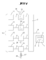
- the Fig. 1 shows an embodiment of the invention.
- the reference numeral 10 designates a source arrangement consisting of four sources 11, 12, 13, 14 in the exemplary embodiment. According to the invention, however, only a single source 11 needs to be present. These single or in the embodiment four sources 11, 12, 13, 14 are each with gas lines 6 with a respective source 11, 12, 13, 14 individually associated modification chamber 21, 22, 23, 24 connected. Each of the modification chambers 21, 22, 23, 24 is connected to a mixing chamber 2. This is done via the gas line designated by the reference numeral 7. Alternatively, one or more sources 11, 12, 13, 14 may be connected directly to the mixing chamber 2 without the interposition of a modification chamber.
- a deposition chamber 1 Downstream of the mixing chamber there is a deposition chamber 1 connected to the gas line 8 with the mixing chamber 2. This has a gas inlet system 3, which is fed by the gas line 8. Below the gas inlet member 3 is a deposition chamber whose bottom is formed by a water-cooled susceptor 4. On the susceptor 4 is a substrate 5, for example in the form of a glass sheet, which is to be coated with an electronic, light-emitting or photovoltaic layer of organic molecules.
- the total pressure in the process chamber is greater than 0.1 mbar and preferably greater than 1 mbar. It can also be greater than 10 mbar, so that the presence of the carrier gas can develop a kinetic effect.
- the organic molecules form solid, liquid or gaseous starting materials which are stored in the sources 11, 12, 13, 14. They are either converted by vaporization into the gas phase or converted by means of injection nozzles into aerosols, which can be transported via a carrier gas stream.
- One of the sources 11, 12, 13, 14 contains a material forming the layer, previously known as the matrix-forming starting material.
- one of the sources 11, 12, 13, 14 contains a starting material which is a precursor of a dopant.
- the modification chambers 21, 22, 23, 24 contain means with which the starting material flowing through this modification chamber 21, 22, 23, 24 can be modified.
- the modification can be a mere physical stimulation. However, it can also be a chemical reaction, for example an analysis or a synthesis. If the chemical reaction is a synthesis, a further reaction gas can be introduced into the modification chamber 21, 24 by means of a reaction gas feed line 26, whereby a plasma cell 27 can also be provided here, with which the reaction gas flowing through the reaction gas feed line 26 , is excited before entering the modification chamber.
- the modification within the modification chamber 21, 22 can take place via a plasma.
- a plasma generator 25 is provided in the modification chamber 21, 22, which generates a DC plasma or an AC plasma. With this plasma, physical excitations or chemical transformations / destruction of the molecules can be made. It is also possible to generate an RF field within a modification chamber 23 to excite or chemically transform the starting materials.
- a heater is provided as a power supply for the modification.
- reaction gas CO, H 2 , TMGa, CH 4 or NH 3 can be passed through the reaction gas line 26.
- H 2 and CH 4 are decomposed in the modification chamber 21 via the plasma generator 25.
- ions or radicals are formed, for example elemental hydrogen, elemental nitrogen or the like. These radicals can be incorporated n-doping in the matrix. These are reducing gases.
- oxidizing gases such as O 3 , N 2 O, O 2 , NO x , SF 6 , CF 4 or halogens such as F 2 , Cl 2 , Br 2 or I 2 may also be used.
- the reaction gases can be decomposed with a plasma into radicals or into ions. If the decomposition product is an ion, then the modification chambers 21, 22, 24 can also have electrostatic filters in order to influence the kinetic energy of these ions.
- Suitable starting materials for a p-doping or an n-doping are also all other chemical compounds known as dopants or precursors of dopants.
- matrix-forming starting materials such as alq 3 or ⁇ -NPD are also suitable.
- the latter are converted with the modification such that they acquire different electronic or optical properties.
Abstract
Description
Die Erfindung betrifft ein Verfahren zum Herstellen insbesondere dotierter Schichten für elektronische, lumineszierende oder photovoltaische Bauelemente, insbesondere OLEDs, wobei ein oder mehrere flüssige oder feste Ausgangsstoffe in einer Quelle verdampfen oder als Aerosol einem Trägergas beigemischt werden und in dieser Form in eine Depositionskammer transportiert werden, wo sie insbesondere in Folge eines Temperaturgradienten eine bevorzugt dotierte Matrix bildend auf einem Substrat kondensieren.The invention relates to a method for producing in particular doped layers for electronic, luminescent or photovoltaic components, in particular OLEDs, wherein one or more liquid or solid starting materials are vaporized in a source or admixed as aerosol to a carrier gas and transported in this form into a deposition chamber, where they condense a preferably doped matrix forming on a substrate, in particular as a result of a temperature gradient.
Die Erfindung betrifft darüber hinaus eine Vorrichtung zur Ausübung des Verfahrens, aufweisend die Quellen und die Quellen mit der Depositionskammer verbindende Gaszuleitungen sowie einen in der Depositionskammer angeordneten Suszeptor zur Aufnahme des Substrates.The invention further relates to a device for performing the method, comprising the sources and the sources with the deposition chamber connecting gas supply lines and arranged in the deposition chamber susceptor for receiving the substrate.
Es ist bekannt, mittels organischer Ausgangsstoffe, die in Form von Salzen oder kleinen Molekülen vorliegen, elektronische, lumineszierende oder photovoltaische Bauelemente herzustellen, wobei diese Ausgangsstoffe durch Transport mittels eines Trägergases einer Depositionskammer zugeleitet werden, wo sie auf einem oder mehreren Substraten, die auf einem Suszeptor angeordnet sind, schichtbildend kondensieren. Als Substrate werden in der Regel Glasscheiben verwendet. Der Suszeptor wird gekühlt, so dass ein Transport der Ausgangsstoffe gegen einen negativen Temperaturgradienten erfolgt.It is known to produce by means of organic starting materials, which are in the form of salts or small molecules, electronic, luminescent or photovoltaic devices, these starting materials are fed by transport by means of a carrier gas of a deposition chamber, where it on one or more substrates on a Susceptor are arranged to condense layer forming. As substrates glass sheets are usually used. The susceptor is cooled, so that a transport of the starting materials takes place against a negative temperature gradient.
Ein sogenannter OVPD-Prozess wird in der
Darüber hinaus werden sogenannte OLEDs (organic light emitting devices) auch in einem thermischen Vakuumverfahren VTE (vacuum thermal evaporation) gefertigt.In addition, so-called OLEDs (organic light emitting devices) are also manufactured in a thermal vacuum process VTE (vacuum thermal evaporation).
Die in der Regel flüssigen oder festen Ausgangsstoffe werden beim OVPD-Prozess in sogenannten Quellen bspw. durch Verdampfen in eine Gasform umgewandelt und dann vorzugsweise unter Verwendung eines Trägergases durch Gasleitungen in eine Depositionskammer transportiert. Dort befindet sich ein Gaseinlassorgan zum verteilten und dosierten Gaseinlass in eine Depositionskammer, in welcher das oben genannte Substrat liegt. Die aus diesen Schichten gefertigten Leuchtdioden (OLEDs) erzeugen bei Stromdurchfluss Licht. Der Stromdurchfluss erfolgt durch Elektronenleitung oder durch Löcherleitung, wobei die Stromdichte nicht nur von der Löcherkonzentration oder der Elektronenkonzentration, sondern auch von deren Beweglichkeit abhängt. Derzeit ist es möglich, OLEDs herzustellen mit einer Effizienz von 20 lm/ W. Zur Steigerung der Effizienz ist es erforderlich, die Leitfähigkeit zu erhöhen. Hierzu werden die abgeschiedenen Schichten elektrisch dotiert. Im Stand der Technik ist es ferner bekannt, stacked OLEDs zu fertigen, indem unterschiedliche oder gleiche OLED-Stapel mit dotierten Zwischenschichten aufeinander abgeschieden werden. Neben Leuchtdioden werden auch Solarzellen mit dem beschriebenen Verfahren gefertigt. Diese photovoltaischen Bauelemente benötigen ebenfalls eine hohe Leitfähigkeit.The generally liquid or solid starting materials are converted into so-called sources in the OVPD process, for example, by evaporation into a gaseous form and then preferably transported by using a carrier gas through gas lines in a deposition chamber. There is a gas inlet member to the distributed and metered gas inlet into a deposition chamber, in which the above-mentioned substrate is located. The light-emitting diodes (OLEDs) produced from these layers generate light when current flows through. The flow of current is effected by electron conduction or by hole conduction, the current density not only depending on the hole concentration or the electron concentration, but also on their mobility. At present, it is possible to produce OLEDs with an efficiency of 20 lm / W. To increase the efficiency, it is necessary to increase the conductivity. For this purpose, the deposited layers are electrically doped. It is also known in the prior art to produce stacked OLEDs by depositing different or identical OLED stacks with doped intermediate layers on one another. In addition to light emitting diodes and solar cells are manufactured with the described method. These photovoltaic devices also require high conductivity.
Neben der elektrischen Dotierung kann auch eine optische Dotierung der Schichten vorgenommen werden.In addition to the electrical doping, an optical doping of the layers can also be carried out.
Das Abscheiden der Schicht und somit auch die Dotierung und insbesondere der Dotierstoffeinbau in die Schicht muss bei Temperaturen deutlich unter 200° C stattfinden, da die verwendeten Ausgangsstoffe sehr temperaturinstabil sind. Eine Prozessvoraussetzung ist daher das Vorhandensein einfach zu handhabender Ausgangsstoffe und insbesondere eines einfach zu handhabenden Dotierstoffs, der sich auch bei Temperaturen unter 200°C und insbesondere Raumtemperatur in die Schichtmatrix einbauen lässt und eine Dotierung bewirkt. Probleme, die mit einem Dotierstoffeinbau einhergehen, dessen Konzentration mindestens zwei Größenordnungen geringer ist als die Matrixkonzentration, werden in "
Anders als bei anorganischen Halbleitern, bei denen man durch gezielte Dotierung Zustände in der Bandlücke einbringen kann, müssen bei organischen Schichten die Ladungsträger auf einem organischen Molekül lokalisiert sein. Wird zusätzlich zu das Matrixmaterial bildenden Ausgangsstoffen ein Dotierstoff verwendet, so ist eine chemische Reaktion (REDOX) zwischen Dotierstoff und Matrixmaterial erforderlich. Diese chemische Reaktion verändert das organische Molekül selbst, so dass dort neue Zustände / Bindungsverhältnisse entstehen. Letzteres muss wegen der Instabilität der verwendete Moleküle bei unter 200°C und insbesondere bei Raumtemperatur stattfinden.In contrast to inorganic semiconductors, in which it is possible to introduce states in the band gap by targeted doping, in organic layers the charge carriers must be located on an organic molecule. If a dopant is used in addition to the matrix material forming starting materials, a chemical reaction (REDOX) between dopant and matrix material is required. This chemical reaction changes the organic molecule itself, creating new states / bonding conditions. The latter must take place because of the instability of the molecules used below 200 ° C and especially at room temperature.
Aus der
Die
Die
Die
Der Erfindung liegt die Aufgabe zugrunde, Maßnahmen anzugeben, mit denen die Dotierung von elektronischen, lumineszierenden oder photovoltaischen Schichten verbessert wird.The invention has for its object to provide measures by which the doping of electronic, luminescent or photovoltaic layers is improved.
Gelöst wird die Aufgabe durch die in den nebengeordneten Ansprüchen 1,10 und 13 angegebene Erfindung, wobei die übrigen Ansprüche vorteilhafte Weiterbildungen der Verfahren bzw. der Vorrichtung sind. Gleichwohl bilden sämtliche fakultativ nebengeordneten Ansprüche aber auch eigenständige Lösung der Aufgabe.The object is achieved by the invention specified in the
Zunächst und im Wesentlichen wird das Verfahren dahingehend weitergebildet, dass der Dotierstoff oder die Dotierung durch Modifikation eines Ausgangsstoffes auf seiner Transportstrecke gebildet werden. Anders als bei der
Dabei kann die Modifikation des Ausgangsstoffs in einer stromabwärts der Quelle und stromaufwärts der Depositionskammer angeordneten Modifikationskammer stattfinden. Die Modifikation ist eine Veränderung des Ausgangsstoffes. Der Ausgangsstoff kann chemisch oder physikalisch verändert werden. Bei der Modifikation kann es sich um eine Stoffumwandlung handeln. Beispielsweise kann der Ausgangsstoff in mehrere Produkte zerlegt werden. Die Modifikation kann sowohl eine Analyse als auch eine Synthese sein. Letztere wird beispielsweise dadurch verwirklicht, dass der Ausgangsstoff mit einem Reaktionspartner reagiert. Der Ausgangsstoff kann mit einem Reaktionspartner chemisch reagieren. Die Dotierung kann erreicht werden, indem ein Ausgangsstoff in geeigneter Weise chemisch umgewandelt wird, so dass die Schicht, die unter Verwendung dieses Ausgangsstoffes gebildet ist, eine höhere elektrische Leitfähigkeit oder eine andere optische Eigenschaft bekommt. Es ist aber auch möglich, dass in der Modifikationskammer lediglich eine katalytische Reaktion stattfindet. Diese kann auch durch Energiezufuhr eingeleitet werden. Alternativ oder in Kombination mit der zuvor genannten Stoffveränderung kann die Modifikation aber auch durch ledigliche Energiezufuhr verursacht werden. Die Energie kann im Wege eines Plasmas dem Ausgangsstoff zugeführt werden. Es ist aber auch möglich, die Energie mittels eines Hochfrequenzgenerators dem Ausgangsstoff zuzufügen. Auch die Verwendung von Wärme und einer die Wärme erzeugenden Heizung kommt in Betracht. Bei dieser Variante wird die Dotierung der Schicht dadurch verursacht, dass ebenfalls ein Ausgangsstoff modifiziert wird, so dass sich die Elektronendichte bzw. die Löcherdichte in der abgeschiedenen Schicht erhöht bzw. sich die optischen Eigenschaften der abgeschiedenen Schicht ändern. Es kann sich hier lediglich um eine energetische Anregung handeln. In einer Variante der Erfindung ist vorgesehen, dass ein den Dotierstoff bildender Ausgangsstoff, also eine Vorstufe des Dotierstoffes modifiziert wird. Die Vorstufe des Dotierstoffes kann selbst nicht in der Lage sein, unter Erhöhung der Leitfähigkeit in die Matrix eingebaut zu werden. Die Vorstufe des Ausgangsstoffes muss dann vielmehr zunächst in der zuvor erwähnten Weise modifiziert werden, um einen Dotierstoff zu erzeugen, der in die Matrix eingebaut werden kann. Dabei erfolgt die Mischung des durch Modifikation eines Ausgangsstoffes erzeugten Dotierstoffs mit ein oder mehreren die Matrix bildenden anderen Ausgangsstoffen in der Modifikationskammer oder in einer Mischkammer, die stromabwärts der Modifikationskammer angeordnet ist. In der Variante, bei der der Dotierstoff durch Modifikation eines Ausgangsstoffes erzeugt wird, würde der Ausgangsstoff ohne Modifikation in der Schicht eine nicht oder schlecht leitende Schicht ausbilden. Er bekommt durch die Modifizierung eine Dotierstoffeigenschaft. Wird dieser modifizierte Ausgangsstoff in die Matrix eingebaut, so wird die elektrische Leitfähigkeit erhöht. Auch hier kann die Modifikation durch Energiezufuhr, durch Synthese oder Analyse erfolgen. Bei der Modifikation können Ionen oder neutrale Radikale gebildet werden. Diese Ionen bzw. neutralen Radikale können die Dotierstofffunktion entfalten. Sie werden über einen Gasstrom bei einem Totaldruck von mehr als 0,1 mbar, insbesondere mehr als 1 mbar in die Prozesskammer geleitet. Die kinetische Energie der bei der Modifikation erzeugten Ionen kann durch elektrische Filter beeinflusst werden. Die elektrischen Filter sind vorzugsweise einer Modifikationskammer zugeordnet. Als matrixbildende Ausgangsstoffe kommen alq3, α-NPD, CuPC oder C60 in Betracht. Als Vorstufe des Dotierstoffes kann insbesondere C60 verwendet werden. Zur Modifikation eines Ausgangsstoffes kann zur Erzeugung eines n-leitenden Dotierstoffs CO, H2 in Verbindung mit einem Plasma, TMGa, CH4 in Verbindung mit einem Plasma oder NH3 verwendet werdet werden. Zur Erzeugung eines p-leitenden Dotierstoffs kann O3, N2O zusammen mit einem Plasma, O2 zusammen mit einem Plasma, NOx, SF6 zusammen mit einem Plasma, CF4 zusammen mit einem Plasma oder irgendein Halogen (F2, Cl2, Br2, I2 ...) verwendet werden. Es ist von Vorteil, wenn zur Modifikation die Bewegungsenergie erzeugter Ionen durch elektrostatische Felder beeinflusst wird. Elektrostatische Felder können eine entsprechend hohe Feldstärke aufweisen. Mit elektrischen Feldern kann auch ein Plasma zur Modifikation erzeugt werden. Dies erfolgt mit einem Gleichspannungsplasmagenerator oder mit einem Wechselspannungsplasmagenerator. Es ist auch vorgesehen, dass eine chemische Reaktion eines der Ausgangsstoffe mit einem Reaktionspartner vor dem Eintritt in die Depositionskammer erfolgt. Eine Vorstufe des Dotierstoffs kann in einer stromaufwärts der Depositionskammer angeordneten Modifikationskammer in einen Dotierstoff umgewandelt werden.The modification of the starting material may take place in a modification chamber located downstream of the source and upstream of the deposition chamber. The modification is a change of the starting material. The starting material can be changed chemically or physically. The modification can be a matter transformation. For example, the starting material can be broken down into several products. The modification can be both an analysis and a synthesis. The latter is achieved, for example, by reacting the starting material with a reaction partner. The starting material can react chemically with a reaction partner. The doping may be achieved by suitably chemically converting a starting material so that the layer formed using this starting material acquires higher electrical conductivity or other optical property. However, it is also possible that only a catalytic reaction takes place in the modification chamber. This can also be initiated by energy. alternative or in combination with the aforementioned change in substance, however, the modification can also be caused by merely supplying energy. The energy can be supplied by way of a plasma to the starting material. But it is also possible to add the energy by means of a high-frequency generator to the starting material. The use of heat and a heat-generating heating is also considered. In this variant, the doping of the layer is caused by the fact that likewise a starting material is modified, so that the electron density or the hole density in the deposited layer increases or the optical properties of the deposited layer change. It can only be an energetic stimulus here. In a variant of the invention, it is provided that a starting material which forms the dopant, that is to say a precursor of the dopant, is modified. The precursor of the dopant itself may not be able to be incorporated into the matrix while increasing conductivity. Rather, the precursor of the precursor must then first be modified in the aforementioned manner to produce a dopant that can be incorporated into the matrix. In this case, the mixture of the dopant produced by modifying a starting material with one or more matrix-forming other starting materials in the modification chamber or in a mixing chamber, which is arranged downstream of the modification chamber. In the variant in which the dopant is produced by modification of a starting material, the starting material would form a non-conductive or poorly conductive layer without modification in the layer. He gets by the modification of a dopant property. If this modified starting material is incorporated into the matrix, the electrical conductivity is increased. Again, the modification can be done by energy, by synthesis or analysis. In the modification, ions or neutral radicals can be formed. These ions or neutral radicals can unfold the dopant function. They are introduced into the process chamber via a gas flow at a total pressure of more than 0.1 mbar, in particular more than 1 mbar directed. The kinetic energy of the ions generated during the modification can be influenced by electrical filters. The electrical filters are preferably associated with a modification chamber. Suitable matrix-forming starting materials are alq 3 , α-NPD, CuPC or C 60 . In particular, C 60 can be used as precursor of the dopant. To modify a starting material, CO, H 2 can be used in conjunction with a plasma, TMGa, CH 4 in conjunction with a plasma or NH 3 to produce an n-type dopant. For producing a p-type dopant, O 3 , N 2 O may be used together with a plasma, O 2 together with a plasma, NO x , SF 6 together with a plasma, CF 4 together with a plasma or any halogen (F 2 , Cl 2 , Br 2 , I 2 ...) can be used. It is advantageous if, for modification, the kinetic energy of generated ions is influenced by electrostatic fields. Electrostatic fields can have a correspondingly high field strength. Electric fields can also be used to create a plasma for modification. This is done with a DC plasma generator or with an AC plasma generator. It is also envisaged that a chemical reaction of one of the starting materials with a reactant takes place prior to entry into the deposition chamber. A precursor of the dopant may be converted into a dopant in a modification chamber located upstream of the deposition chamber.
Die Erfindung betrifft darüber hinaus ein Verfahren, bei dem die Modifikationskammer die Funktion einer "Crack-Kammer" besitzt. Bei dieser Variation wird in der Modifikationskammer lediglich ein Ausgangsstoff zerstört. Es kann sich dabei um einen die Matrix bildenden Ausgangsstoff oder um einen durch Modifikation die Dotierung bzw. den Dotierstoff bildenden Ausgangsstoff handeln. Im ersten Fall wird durch die temporäre Zerstörung des Ausgangsstoffes das Wachstum der Schicht unterbrochen. Die Zerlegungsprodukte des zerstörten Ausgangsstoffs sind nicht in der Lage, schichtbildend auf dem Substrat zu kondensieren. Letzteres kann nur der Ausgangsstoff im unzerstörten Zustand. Sobald die Zerstörung des Ausgangsstoffes, die beispielsweise mittels eines Plasmas erfolgen kann, aufhört, wird das Schichtwachstum fortgesetzt. Hierdurch ist ein virtuelles Run-Vent-System gegeben. Der Dotierstoffeinbau kann in analoger Weise ein- und ausgeschaltet werden, wobei entweder bei Plasma-Anwendung der Dotierstoff gebildet wird oder bei Plasma-Anwendung ein Vorprodukt des Dotierstoffs oder der Dotierstoff selbst derartig zerstört wird, dass kein Dotierstoffeinbau stattfindet. Als Trägergas können die bekannten Trägergase wie Wasserstoff, Stickstoff oder ein geeignetes Edelgas / Inertgas verwendet werden. Das Verfahren kann bei einem Totaldruck von 1 mbar durchgeführt werden. Das Verfahren kann in einer Vorrichtung durchgeführt werden, bei der es sich um einen bekannten OVPD-Reaktor handelt, der ein oder mehrere Quellen aufweist sowie Gasleitungen zwischen Quellen und einer Depositionskammer. Es können die die Matrix bildenden Ausgangsstoffe und/oder die einen oder mehrere Dotierstoffe bildenden Ausgangsstoffe zerstört werden. Es kann sich dabei jeweils auch nur um einen einzigen Ausgangsstoff handeln, der temporär zerstört wird. Die Zerstörung kann durch ein Plasma erfolgen. Somit kann durch Ein- und Ausschalten der Energiezufuhr, insbesondere des Plasmas, das Schichtwachstum bzw. die Dotierung aus- und wieder eingeschaltet werden. Dieser OVPD-Reaktor wird erfindungsgemäß dadurch weitergebildet, dass stromabwärts der ein oder mehreren Quellen und stromaufwärts der Depositionskammer ein oder mehrere Modifikationskammern vorgesehen sind. In dieser Modifikationskammer kann ein Ausgangsstoff durch Energiezufuhr und / oder durch Reaktionsgaszufuhr modifiziert werden. Die Modifikationskammer kann einen Plasma-Generator umfassen, in dem ein Gleichspannungsplasma oder ein Wechselspannungsplasma erzeugt werden. Darüber hinaus kann die Modifikationskammer einen Hochfrequenzgenerator umfassen, um ein RF-Feld aufzubauen, mit dem der Ausgangsstoff modifiziert werden kann. Die Modifikationskammer kann auch einen Gaseinlass zum Einlass eines Reaktionsgases oder eine Heizung umfassen. Zwischen der ein oder mehreren Modifikationskammer und der Depositionskammer kann sich eine Mischkammer befinden, in welche Gasleitungen mehrerer Quellen münden. Beispielsweise kann in einer Quelle als Ausgangsstoff eine Vorstufe des Dotierstoffs bereitgestellt werden. Dieser Ausgangsstoff wird über einen Trägergasstrom in die Modifikationskammer geleitet. In dieser Modifikationskammer wird die Vorstufe des Dotierstoffes modifiziert zu einem Dotierstoff, der dann mit dem Gasstrom in die Mischkammer geleitet wird. In mindestens einer anderen Quelle kann bei dieser Variante ein eine Matrix bildender Ausgangsstoff bereitgestellt werden. Dieser kann direkt oder ebenfalls durch eine Modifikationskammer strömend der Mischkammer zugeleitet werden. Dotierstoff und matrixbildender Ausgangsstoff werden in der Mischkammer homogenisiert. Dort kann bereits eine Gasphasenreaktion stattfinden. Die Konzentrationsverhältnisse sind so gewählt, dass der Dotierstoff in etwa hundertmal geringerer Konzentration in der Gasphase vorkommt als der matrixbildende Ausgangsstoff. Das Gasgemisch wird in die Depositionskammer geleitet und kondensiert auf dem Substrat, welches sich auf einem gekühlten Suszeptor befinden kann. Die Bereitstellung der Ausgangsstoffe erfolgt in der im Stand der Technik beschriebenen Weise, nämlich insbesondere durch Bildung von Aerosolen oder durch Verdampfen eines Festkörpers oder einer Flüssigkeit. In einer Weiterbildung der Erfindung wird ein Reaktionsgas als Ausgangsstoff in die Modifikationskammer geleitet. Der Modifikationskammer kann eine Plasmazelle vorgeordnet sein, in der das Reaktionsgas mit einem Plasma behandelt werden kann. Das Plasma kann zur Aktivierung des Reaktionsgases dienen.The invention further relates to a method in which the modification chamber has the function of a "cracking chamber". In this variation, only one source is destroyed in the modification chamber. It can be a starting material which forms the matrix or a starting material which forms the doping or the dopant by modification. In the first case, the growth of the layer is interrupted by the temporary destruction of the starting material. The decomposition products of the destroyed source are unable to form on the substrate to condense. The latter can only the starting material in the undestroyed state. As soon as the destruction of the starting material, which can take place for example by means of a plasma, ceases, the layer growth is continued. This gives a virtual run-vent system. The dopant incorporation can be switched on and off in an analogous manner, wherein the dopant is formed either during plasma application or, in the case of plasma application, a precursor of the dopant or the dopant itself is destroyed in such a way that no dopant incorporation takes place. As a carrier gas, the known carrier gases such as hydrogen, nitrogen or a suitable inert gas / inert gas can be used. The process can be carried out at a total pressure of 1 mbar. The process may be carried out in a device which is a known OVPD reactor having one or more sources and gas lines between sources and a deposition chamber. The starting materials forming the matrix and / or the starting materials which form one or more dopants can be destroyed. It can also be only a single starting material, which is temporarily destroyed. The destruction can be done by a plasma. Thus, by switching on and off the power supply, in particular of the plasma, the layer growth or the doping off and on again. According to the invention, this OVPD reactor is further developed in that one or more modification chambers are provided downstream of the one or more sources and upstream of the deposition chamber. In this modification chamber, a starting material can be modified by supplying energy and / or by supplying reaction gas. The modification chamber may include a plasma generator in which a DC plasma or an AC plasma is generated. In addition, the modification chamber may include a high frequency generator to build up an RF field with which the source material can be modified. The modification chamber may also include a gas inlet to the inlet of a reaction gas or a heater. Between the one or more modification chamber and the deposition chamber may be located a mixing chamber into which gas lines of several sources. For example, a precursor of the dopant can be provided in a source as the starting material. This starting material is passed through a carrier gas stream in the modification chamber. In this modification chamber, the precursor of the dopant is modified to a dopant, which is then passed with the gas flow in the mixing chamber. In at least one other source, a starting material forming a matrix can be provided in this variant. This can be fed directly or also by a modification chamber flowing the mixing chamber. Dopant and matrix-forming starting material are homogenized in the mixing chamber. There may already take place a gas phase reaction. The concentration ratios are chosen so that the dopant occurs in about one hundred times lower concentration in the gas phase than the matrix-forming starting material. The gas mixture is passed into the deposition chamber and condenses on the substrate, which may be on a cooled susceptor. The preparation of the starting materials is carried out in the manner described in the prior art, namely in particular by formation of aerosols or by evaporation of a solid or a liquid. In one development of the invention, a reaction gas is passed as starting material into the modification chamber. The modification chamber may be preceded by a plasma cell in which the reaction gas can be treated with a plasma. The plasma can serve to activate the reaction gas.
Die
Stromabwärts der Mischkammer befindet sich eine mit der Gasleitung 8 mit der Mischkammer 2 verbundene Depositionskammer 1. Diese weist ein Gaseinlasssystem 3 auf, welches von der Gasleitung 8 gespeist wird. Unterhalb des Gaseinlassorgans 3 befindet sich eine Depositionskammer, deren Boden von einem wassergekühlten Suszeptor 4 gebildet wird. Auf dem Suszeptor 4 liegt ein Substrat 5, beispielsweise in Form einer Glasscheibe, welche mit einer elektronischen, lichtemittierenden oder photovoltaischen Schicht aus organischen Molekülen beschichtet werden soll. Der Totaldruck in der Prozesskammer ist größer als 0,1 mbar und bevorzugt größer als 1 mbar. Er kann auch größer als 10 mbar sein, so dass die Anwesenheit des Trägergases eine kinetische Wirkung entfalten kann.Downstream of the mixing chamber there is a
Die organischen Moleküle bilden feste, flüssige oder gasförmige Ausgangsstoffe, die in den Quellen 11, 12, 13, 14 bevorratet werden. Sie werden dort entweder durch Verdampfen in die Gasphase überführt oder mittels Injektionsdüsen in Aerosole umgewandelt, die über einen Trägergasstrom transportiert werden können.The organic molecules form solid, liquid or gaseous starting materials which are stored in the
Eine der Quellen 11, 12, 13, 14 enthält ein die Schicht bildendes, zuvor als matrixbildenden Ausgangsstoff bezeichnetes Material.One of the
Es ist auch möglich, dass eine der Quellen 11, 12, 13, 14 einen Ausgangsstoff enthält, der eine Vorstufe eines Dotierstoffs ist.It is also possible that one of the
Die Modifikationskammern 21, 22, 23, 24 enthalten Einrichtungen, mit denen der durch diese Modifikationskammer 21, 22, 23, 24 strömende Ausgangsstoff modifiziert werden kann. Die Modifikation kann dabei eine ledigliche physikalische Anregung sein. Sie kann aber auch eine chemische Reaktion, bspw. eine Analyse oder eine Synthese sein. Handelt es sich bei der chemischen Reaktion um eine Synthese, so kann durch eine Reaktionsgaszuleitung 26 ein weiteres Reaktionsgas in die Modifikationskammer 21, 24 eingeleitet werden, wobei hier auch eine Plasmazelle 27 vorsehen sein kann, mit der das Reaktionsgas, welches durch die Reaktionsgaszuleitung 26 strömt, vor dem Eintritt in die Modifikationskammer angeregt wird.The
Die Modifikation innerhalb der Modifikationskammer 21, 22 kann über ein Plasma erfolgen. Hierzu ist in der Modifikationskammer 21, 22 ein Plasmagenerator 25 vorgesehen, der ein Gleichspannungsplasma oder ein Wechselspannungsplasma erzeugt. Mit diesem Plasma können physikalische Anregungen oder chemische Umformungen / Zerstörungen der Moleküle vorgenommen werden. Es ist ebenfalls möglich, innerhalb einer Modifikationskammer 23 ein RF-Feld zu erzeugen, um die Ausgangsstoffe anzuregen oder chemisch umzuwandeln. Schließlich ist als Energiezufuhr für die Modifikation auch eine Heizung vorgesehen.The modification within the
Als Reaktionsgas kann durch die Reaktionsgasleitung 26 CO, H2, TMGa, CH4 oder NH3 geleitet werden. H2 und CH4 werden in der Modifikationskammer 21 über den Plasma-Generator 25 zerlegt. Eine derartige Zerlegung kann aber auch vor der Modifikationskammer 24 mit der Plasmazelle 27 durchgeführt werden. Bei der Zerlegung entstehen Ionen oder Radikale, bspw. elementarer Wasserstoff, elementarer Stickstoff oder dergleichen. Diese Radikale können n-dotierend in die Matrix eingebaut werden. Es handelt sich dabei um reduzierende Gase. Alternativ können auch oxidierende Gase wie O3, N2O, O2, NOx, SF6, CF4 oder Halogene wie F2, Cl2, Br2 oder I2 verwendet werden. Auch hier können die Reaktionsgase mit einem Plasma in Radikale oder in Ionen zerlegt werden. Ist das Zerlegungsprodukt ein Ion, so können die Modifikationskammern 21, 22, 24 auch elektrostatische Filter besitzen, um die kinetische Energie dieser Ionen zu beeinflussen.As the reaction gas, CO, H 2 , TMGa, CH 4 or NH 3 can be passed through the
Als Ausgangsstoffe für eine p-Dotierung oder eine n-Dotierung kommen auch alle anderen, als Dotierstoffe oder Vorstufen von Dotierstoffen bekannten chemischen Verbindungen in Betracht.Suitable starting materials for a p-doping or an n-doping are also all other chemical compounds known as dopants or precursors of dopants.
In Betracht kommen schließlich auch die matrixbildenden Ausgangsstoffe wie alq3 oder α-NPD. Letztere werden mit der Modifikation derart umgewandelt, dass sie andere elektronische oder optische Eigenschaften bekommen.Finally, the matrix-forming starting materials such as alq 3 or α-NPD are also suitable. The latter are converted with the modification such that they acquire different electronic or optical properties.
Mit der in
Alle offenbarten Merkmale sind (für sich) erfindungswesentlich. In die Offenbarung der Anmeldung wird hiermit auch der Offenbarungsinhalt der zugehörigen/beigefügten Prioritätsunterlagen (Abschrift der Voranmeldung) vollinhaltlich mit einbezogen, auch zu dem Zweck, Merkmale dieser Unterlagen in Ansprüche vorliegender Anmeldung mit aufzunehmen.All disclosed features are essential to the invention. The disclosure content of the associated / attached priority documents (copy of the prior application) is hereby also incorporated in full in the disclosure of the application also for the purpose of incorporating features of these documents in claims of the present application.
Claims (15)
Applications Claiming Priority (1)
| Application Number | Priority Date | Filing Date | Title |
|---|---|---|---|
| DE102007030499A DE102007030499A1 (en) | 2007-06-30 | 2007-06-30 | Apparatus and method for depositing in particular doped layers by means of OVPD or the like |
Publications (3)
| Publication Number | Publication Date |
|---|---|
| EP2009714A2 true EP2009714A2 (en) | 2008-12-31 |
| EP2009714A3 EP2009714A3 (en) | 2012-02-29 |
| EP2009714B1 EP2009714B1 (en) | 2018-12-05 |
Family
ID=39862959
Family Applications (1)
| Application Number | Title | Priority Date | Filing Date |
|---|---|---|---|
| EP08159270.1A Expired - Fee Related EP2009714B1 (en) | 2007-06-30 | 2008-06-27 | Method and device for deposition of doped layers by means of OVPD or similar |
Country Status (3)
| Country | Link |
|---|---|
| US (1) | US8304013B2 (en) |
| EP (1) | EP2009714B1 (en) |
| DE (1) | DE102007030499A1 (en) |
Cited By (1)
| Publication number | Priority date | Publication date | Assignee | Title |
|---|---|---|---|---|
| WO2016037964A1 (en) * | 2014-09-08 | 2016-03-17 | Cynora Gmbh | Improved optically active layer and method for the production thereof |
Families Citing this family (4)
| Publication number | Priority date | Publication date | Assignee | Title |
|---|---|---|---|---|
| DE102014100135A1 (en) | 2014-01-08 | 2015-07-09 | Aixtron Se | Gas mixing device on a reactor with directional valve |
| JP2016222984A (en) * | 2015-06-01 | 2016-12-28 | 株式会社フィルテック | Heat beam deposition apparatus |
| KR102369676B1 (en) | 2017-04-10 | 2022-03-04 | 삼성디스플레이 주식회사 | Apparatus and method for manufacturing a display apparatus |
| KR20190090414A (en) * | 2018-01-24 | 2019-08-02 | 삼성디스플레이 주식회사 | Deposition apparatus |
Citations (5)
| Publication number | Priority date | Publication date | Assignee | Title |
|---|---|---|---|---|
| DD279032A1 (en) | 1988-12-30 | 1990-05-23 | Elektronische Bauelemente Veb | PROCESS FOR PRODUCING DUENNER ORGANIC SEMICONDUCTOR LAYERS |
| US5554220A (en) | 1995-05-19 | 1996-09-10 | The Trustees Of Princeton University | Method and apparatus using organic vapor phase deposition for the growth of organic thin films with large optical non-linearities |
| US6207238B1 (en) | 1998-12-16 | 2001-03-27 | Battelle Memorial Institute | Plasma enhanced chemical deposition for high and/or low index of refraction polymers |
| DE10338406A1 (en) | 2003-08-18 | 2005-03-24 | Novaled Gmbh | Doped organic semiconductor materials and process for their preparation |
| US7201942B2 (en) | 2000-02-16 | 2007-04-10 | Aixtron Ag | Coating method |
Family Cites Families (10)
| Publication number | Priority date | Publication date | Assignee | Title |
|---|---|---|---|---|
| US5156815A (en) * | 1988-09-08 | 1992-10-20 | Board Of Regents, The University Of Texas System | Sublimating and cracking apparatus |
| DE19822333A1 (en) * | 1998-05-19 | 1999-12-02 | Lutz Kipp | Fullerites used in manufacture of electronic components |
| US6228436B1 (en) * | 1998-12-16 | 2001-05-08 | Battelle Memorial Institute | Method of making light emitting polymer composite material |
| US7109518B2 (en) * | 2000-06-19 | 2006-09-19 | Yokohama Tlo Company, Ltd. | Electronic element operable at room temperature using super-dielectric phenomenon |
| DE10207859A1 (en) * | 2002-02-20 | 2003-09-04 | Univ Dresden Tech | Doped organic semiconductor material and process for its production |
| DE10212923A1 (en) * | 2002-03-22 | 2004-01-08 | Aixtron Ag | Process for coating a substrate and device for carrying out the process |
| US20050109281A1 (en) * | 2002-03-22 | 2005-05-26 | Holger Jurgensen | Process for coating a substrate, and apparatus for carrying out the process |
| JP4342445B2 (en) * | 2002-07-19 | 2009-10-14 | ピーピージー・インダストリーズ・オハイオ・インコーポレイテッド | Article having nanoscale structure and method for producing the article |
| EP1607446B1 (en) * | 2003-03-26 | 2016-09-07 | Semiconductor Energy Laboratory Co., Ltd. | Organic/inorganic hybrid material, composition for synthesizing the same and process for producing the hybrid material |
| US7238389B2 (en) * | 2004-03-22 | 2007-07-03 | Eastman Kodak Company | Vaporizing fluidized organic materials |
-
2007
- 2007-06-30 DE DE102007030499A patent/DE102007030499A1/en not_active Withdrawn
-
2008
- 2008-06-27 US US12/163,546 patent/US8304013B2/en active Active
- 2008-06-27 EP EP08159270.1A patent/EP2009714B1/en not_active Expired - Fee Related
Patent Citations (5)
| Publication number | Priority date | Publication date | Assignee | Title |
|---|---|---|---|---|
| DD279032A1 (en) | 1988-12-30 | 1990-05-23 | Elektronische Bauelemente Veb | PROCESS FOR PRODUCING DUENNER ORGANIC SEMICONDUCTOR LAYERS |
| US5554220A (en) | 1995-05-19 | 1996-09-10 | The Trustees Of Princeton University | Method and apparatus using organic vapor phase deposition for the growth of organic thin films with large optical non-linearities |
| US6207238B1 (en) | 1998-12-16 | 2001-03-27 | Battelle Memorial Institute | Plasma enhanced chemical deposition for high and/or low index of refraction polymers |
| US7201942B2 (en) | 2000-02-16 | 2007-04-10 | Aixtron Ag | Coating method |
| DE10338406A1 (en) | 2003-08-18 | 2005-03-24 | Novaled Gmbh | Doped organic semiconductor materials and process for their preparation |
Non-Patent Citations (4)
| Title |
|---|
| FENGHONG LI ET AL.: "Novel dopants for n-type doping of electron transport materials: cationic dyes and their bases", DISSERTATION, DIPL.-CHEM., January 2005 (2005-01-01) |
| P. E. BURROWS: "Organic Vapor Phase Depo sition: a New Method for the Growth of Organic Thin Films with Large Optical Non-linearities", CRYSTAL GROWTH, vol. 156, 1995, pages 91 |
| S. R. FORREST ET AL.: "Intense Second Harmonic Generation and Long-Range Structural Ordering in Thin Films of an Organic Salt Grown by Organic Vapor Phase Deposition", APPL. PHYS. LETT., vol. 68, 1996, pages 1326, XP000582290, DOI: doi:10.1063/1.115923 |
| SHIN-ICHIRO TAMURA: "A Blue Organic Light Emitting Diode", JPN. J. APPL. PHYS., vol. 38, no. 9A, 1999, pages 5274 - 5277 |
Cited By (1)
| Publication number | Priority date | Publication date | Assignee | Title |
|---|---|---|---|---|
| WO2016037964A1 (en) * | 2014-09-08 | 2016-03-17 | Cynora Gmbh | Improved optically active layer and method for the production thereof |
Also Published As
| Publication number | Publication date |
|---|---|
| US20090004830A1 (en) | 2009-01-01 |
| US8304013B2 (en) | 2012-11-06 |
| DE102007030499A1 (en) | 2009-01-08 |
| EP2009714A3 (en) | 2012-02-29 |
| EP2009714B1 (en) | 2018-12-05 |
Similar Documents
| Publication | Publication Date | Title |
|---|---|---|
| DE69827293T2 (en) | STEAM PHASE SEPARATION OF ORGANIC THIN LAYERS AT LOW PRESSURE | |
| DE102008011185A1 (en) | Process for producing a doped organic semiconducting layer | |
| DE102007014048B4 (en) | Mixture of matrix material and doping material, and method for producing a layer of doped organic material | |
| DE102006054523B4 (en) | Dithiolene transition metal complexes and selenium-analogous compounds, their use as dopant, organic semiconductive material containing the complexes, and electronic or optoelectronic device containing a complex | |
| DE102013109451B9 (en) | Method for producing an optoelectronic component | |
| DE102008056391B4 (en) | Organic electronic component and process for its manufacture | |
| DE10333232A1 (en) | Organic electroluminescent element | |
| EP2009714B1 (en) | Method and device for deposition of doped layers by means of OVPD or similar | |
| WO2008058525A2 (en) | Use of a coordination compound for the doping of organic semiconductors | |
| EP1859494A1 (en) | Photoactive component with organic layers | |
| DE102013021223A1 (en) | Production of flexible organic electronic devices | |
| EP1860709A1 (en) | Use of square planar transition metal complexes as dopants | |
| WO2014076276A1 (en) | Method for producing a layer on a surface area of an electronic component | |
| WO2016000944A1 (en) | Device and method for generating vapor for a cvd- or pvd device from multiple liquid or solid source materials | |
| DE112020003405T5 (en) | Method of making a polymer-coated graphene layered structure and graphene layered structure | |
| WO2016050330A1 (en) | Method for producing an organic electronic component, and organic electronic component | |
| EP3230295A1 (en) | Amino phosphazene bases as n-dopants in organic electronics | |
| EP0958241B1 (en) | PROCESS AND DEVICE FOR PRODUCING STABLE ENDOHEDRAL FULLERENES OF STRUCTURE Z-at-Cx WITH x GREATER THAN OR EQUAL TO 60 | |
| EP1783846B1 (en) | Deposition of a doped organic material on a substrate | |
| WO2021078584A1 (en) | Method for depositing organic layer structures, in particular oleds | |
| WO2019068607A1 (en) | Method for producing a luminous pixel arrangement | |
| DE102012102565A1 (en) | Method for producing an electrical component, code position system and electrical component | |
| WO2023131379A1 (en) | Method for producing a photoactive layer in a layer system of an organic electronic component | |
| EP3221422A1 (en) | Copper(i) complexes for optoelectronic applications | |
| DE102019103188A1 (en) | Method, sputter target and processing arrangement |
Legal Events
| Date | Code | Title | Description |
|---|---|---|---|
| PUAI | Public reference made under article 153(3) epc to a published international application that has entered the european phase |
Free format text: ORIGINAL CODE: 0009012 |
|
| AK | Designated contracting states |
Kind code of ref document: A2 Designated state(s): AT BE BG CH CY CZ DE DK EE ES FI FR GB GR HR HU IE IS IT LI LT LU LV MC MT NL NO PL PT RO SE SI SK TR |
|
| AX | Request for extension of the european patent |
Extension state: AL BA MK RS |
|
| RAP1 | Party data changed (applicant data changed or rights of an application transferred) |
Owner name: AIXTRON AG |
|
| RAP1 | Party data changed (applicant data changed or rights of an application transferred) |
Owner name: AIXTRON SE |
|
| RIC1 | Information provided on ipc code assigned before grant |
Ipc: H01L 51/00 20060101ALI20111013BHEP Ipc: B05D 7/24 20060101AFI20111013BHEP Ipc: C23C 14/22 20060101ALI20111013BHEP Ipc: C23C 14/54 20060101ALI20111013BHEP Ipc: H01L 51/52 20060101ALI20111013BHEP Ipc: H01L 51/56 20060101ALI20111013BHEP Ipc: C23C 14/12 20060101ALI20111013BHEP |
|
| PUAL | Search report despatched |
Free format text: ORIGINAL CODE: 0009013 |
|
| AK | Designated contracting states |
Kind code of ref document: A3 Designated state(s): AT BE BG CH CY CZ DE DK EE ES FI FR GB GR HR HU IE IS IT LI LT LU LV MC MT NL NO PL PT RO SE SI SK TR |
|
| AX | Request for extension of the european patent |
Extension state: AL BA MK RS |
|
| RIC1 | Information provided on ipc code assigned before grant |
Ipc: C23C 14/22 20060101ALI20120126BHEP Ipc: C23C 14/54 20060101ALI20120126BHEP Ipc: H01L 51/52 20060101ALI20120126BHEP Ipc: H01L 51/56 20060101ALI20120126BHEP Ipc: C23C 14/12 20060101ALI20120126BHEP Ipc: H01L 51/00 20060101ALI20120126BHEP Ipc: C23C 14/24 20060101ALI20120126BHEP Ipc: B05D 1/00 20060101AFI20120126BHEP Ipc: C23C 14/32 20060101ALI20120126BHEP |
|
| 17P | Request for examination filed |
Effective date: 20120719 |
|
| AKX | Designation fees paid |
Designated state(s): DE FR GB NL |
|
| RAP1 | Party data changed (applicant data changed or rights of an application transferred) |
Owner name: AIXTRON SE |
|
| STAA | Information on the status of an ep patent application or granted ep patent |
Free format text: STATUS: EXAMINATION IS IN PROGRESS |
|
| 17Q | First examination report despatched |
Effective date: 20180119 |
|
| GRAP | Despatch of communication of intention to grant a patent |
Free format text: ORIGINAL CODE: EPIDOSNIGR1 |
|
| STAA | Information on the status of an ep patent application or granted ep patent |
Free format text: STATUS: GRANT OF PATENT IS INTENDED |
|
| INTG | Intention to grant announced |
Effective date: 20180713 |
|
| GRAS | Grant fee paid |
Free format text: ORIGINAL CODE: EPIDOSNIGR3 |
|
| GRAA | (expected) grant |
Free format text: ORIGINAL CODE: 0009210 |
|
| GRAA | (expected) grant |
Free format text: ORIGINAL CODE: 0009210 |
|
| STAA | Information on the status of an ep patent application or granted ep patent |
Free format text: STATUS: THE PATENT HAS BEEN GRANTED |
|
| AK | Designated contracting states |
Kind code of ref document: B1 Designated state(s): DE FR GB NL |
|
| REG | Reference to a national code |
Ref country code: GB Ref legal event code: FG4D Free format text: NOT ENGLISH |
|
| REG | Reference to a national code |
Ref country code: DE Ref legal event code: R096 Ref document number: 502008016500 Country of ref document: DE |
|
| REG | Reference to a national code |
Ref country code: NL Ref legal event code: MP Effective date: 20181205 |
|
| PG25 | Lapsed in a contracting state [announced via postgrant information from national office to epo] |
Ref country code: NL Free format text: LAPSE BECAUSE OF FAILURE TO SUBMIT A TRANSLATION OF THE DESCRIPTION OR TO PAY THE FEE WITHIN THE PRESCRIBED TIME-LIMIT Effective date: 20181205 |
|
| REG | Reference to a national code |
Ref country code: DE Ref legal event code: R097 Ref document number: 502008016500 Country of ref document: DE |
|
| PLBE | No opposition filed within time limit |
Free format text: ORIGINAL CODE: 0009261 |
|
| STAA | Information on the status of an ep patent application or granted ep patent |
Free format text: STATUS: NO OPPOSITION FILED WITHIN TIME LIMIT |
|
| 26N | No opposition filed |
Effective date: 20190906 |
|
| GBPC | Gb: european patent ceased through non-payment of renewal fee |
Effective date: 20190627 |
|
| PG25 | Lapsed in a contracting state [announced via postgrant information from national office to epo] |
Ref country code: GB Free format text: LAPSE BECAUSE OF NON-PAYMENT OF DUE FEES Effective date: 20190627 |
|
| PG25 | Lapsed in a contracting state [announced via postgrant information from national office to epo] |
Ref country code: FR Free format text: LAPSE BECAUSE OF NON-PAYMENT OF DUE FEES Effective date: 20190630 |
|
| PGFP | Annual fee paid to national office [announced via postgrant information from national office to epo] |
Ref country code: DE Payment date: 20200716 Year of fee payment: 13 |
|
| REG | Reference to a national code |
Ref country code: DE Ref legal event code: R119 Ref document number: 502008016500 Country of ref document: DE |
|
| PG25 | Lapsed in a contracting state [announced via postgrant information from national office to epo] |
Ref country code: DE Free format text: LAPSE BECAUSE OF NON-PAYMENT OF DUE FEES Effective date: 20220101 |