EP2040309A2 - Thin inverted metamorphic multijunction solar cells with rigid support - Google Patents
Thin inverted metamorphic multijunction solar cells with rigid support Download PDFInfo
- Publication number
- EP2040309A2 EP2040309A2 EP08013466A EP08013466A EP2040309A2 EP 2040309 A2 EP2040309 A2 EP 2040309A2 EP 08013466 A EP08013466 A EP 08013466A EP 08013466 A EP08013466 A EP 08013466A EP 2040309 A2 EP2040309 A2 EP 2040309A2
- Authority
- EP
- European Patent Office
- Prior art keywords
- subcell
- solar cell
- band gap
- solar
- substrate
- Prior art date
- Legal status (The legal status is an assumption and is not a legal conclusion. Google has not performed a legal analysis and makes no representation as to the accuracy of the status listed.)
- Withdrawn
Links
- 239000000758 substrate Substances 0.000 claims abstract description 64
- 239000006059 cover glass Substances 0.000 claims abstract description 16
- 239000011229 interlayer Substances 0.000 claims abstract description 13
- 239000010410 layer Substances 0.000 claims description 117
- 238000000034 method Methods 0.000 claims description 48
- 229910052751 metal Inorganic materials 0.000 claims description 20
- 239000002184 metal Substances 0.000 claims description 20
- 239000004065 semiconductor Substances 0.000 claims description 19
- 239000000463 material Substances 0.000 claims description 13
- 238000004519 manufacturing process Methods 0.000 claims description 9
- 240000002329 Inga feuillei Species 0.000 claims description 6
- 238000005530 etching Methods 0.000 claims description 6
- 229910001218 Gallium arsenide Inorganic materials 0.000 claims description 5
- 238000000151 deposition Methods 0.000 claims description 5
- 229910000530 Gallium indium arsenide Inorganic materials 0.000 claims description 3
- 239000004020 conductor Substances 0.000 claims description 3
- 238000000227 grinding Methods 0.000 claims description 3
- 239000011521 glass Substances 0.000 claims description 2
- 239000010980 sapphire Substances 0.000 claims description 2
- 229910052594 sapphire Inorganic materials 0.000 claims description 2
- 238000003466 welding Methods 0.000 claims 1
- 210000004027 cell Anatomy 0.000 description 119
- 239000000853 adhesive Substances 0.000 description 9
- 230000001070 adhesive effect Effects 0.000 description 9
- 235000012431 wafers Nutrition 0.000 description 8
- 230000004888 barrier function Effects 0.000 description 7
- 239000000203 mixture Substances 0.000 description 6
- 230000006798 recombination Effects 0.000 description 6
- 238000005215 recombination Methods 0.000 description 6
- 230000003667 anti-reflective effect Effects 0.000 description 5
- GNPVGFCGXDBREM-UHFFFAOYSA-N germanium atom Chemical compound [Ge] GNPVGFCGXDBREM-UHFFFAOYSA-N 0.000 description 4
- 239000010409 thin film Substances 0.000 description 4
- CIWBSHSKHKDKBQ-JLAZNSOCSA-N Ascorbic acid Chemical compound OC[C@H](O)[C@H]1OC(=O)C(O)=C1O CIWBSHSKHKDKBQ-JLAZNSOCSA-N 0.000 description 3
- 230000008901 benefit Effects 0.000 description 3
- 238000006243 chemical reaction Methods 0.000 description 3
- KRKNYBCHXYNGOX-UHFFFAOYSA-N citric acid Chemical compound OC(=O)CC(O)(C(O)=O)CC(O)=O KRKNYBCHXYNGOX-UHFFFAOYSA-N 0.000 description 3
- 229910052732 germanium Inorganic materials 0.000 description 3
- IJGRMHOSHXDMSA-UHFFFAOYSA-N Atomic nitrogen Chemical compound N#N IJGRMHOSHXDMSA-UHFFFAOYSA-N 0.000 description 2
- XUIMIQQOPSSXEZ-UHFFFAOYSA-N Silicon Chemical compound [Si] XUIMIQQOPSSXEZ-UHFFFAOYSA-N 0.000 description 2
- 238000013459 approach Methods 0.000 description 2
- 229910052799 carbon Inorganic materials 0.000 description 2
- 238000010276 construction Methods 0.000 description 2
- 230000001419 dependent effect Effects 0.000 description 2
- 239000002019 doping agent Substances 0.000 description 2
- 230000006911 nucleation Effects 0.000 description 2
- 238000010899 nucleation Methods 0.000 description 2
- 229910052710 silicon Inorganic materials 0.000 description 2
- 239000010703 silicon Substances 0.000 description 2
- 241000894007 species Species 0.000 description 2
- 239000000126 substance Substances 0.000 description 2
- 229910000980 Aluminium gallium arsenide Inorganic materials 0.000 description 1
- JBRZTFJDHDCESZ-UHFFFAOYSA-N AsGa Chemical compound [As]#[Ga] JBRZTFJDHDCESZ-UHFFFAOYSA-N 0.000 description 1
- ZOXJGFHDIHLPTG-UHFFFAOYSA-N Boron Chemical compound [B] ZOXJGFHDIHLPTG-UHFFFAOYSA-N 0.000 description 1
- OKTJSMMVPCPJKN-UHFFFAOYSA-N Carbon Chemical compound [C] OKTJSMMVPCPJKN-UHFFFAOYSA-N 0.000 description 1
- -1 GaInPAs Inorganic materials 0.000 description 1
- GYHNNYVSQQEPJS-UHFFFAOYSA-N Gallium Chemical compound [Ga] GYHNNYVSQQEPJS-UHFFFAOYSA-N 0.000 description 1
- ATJFFYVFTNAWJD-UHFFFAOYSA-N Tin Chemical compound [Sn] ATJFFYVFTNAWJD-UHFFFAOYSA-N 0.000 description 1
- 229910052782 aluminium Inorganic materials 0.000 description 1
- XAGFODPZIPBFFR-UHFFFAOYSA-N aluminium Chemical compound [Al] XAGFODPZIPBFFR-UHFFFAOYSA-N 0.000 description 1
- 229910052787 antimony Inorganic materials 0.000 description 1
- WATWJIUSRGPENY-UHFFFAOYSA-N antimony atom Chemical compound [Sb] WATWJIUSRGPENY-UHFFFAOYSA-N 0.000 description 1
- 238000003491 array Methods 0.000 description 1
- 229910052785 arsenic Inorganic materials 0.000 description 1
- RQNWIZPPADIBDY-UHFFFAOYSA-N arsenic atom Chemical compound [As] RQNWIZPPADIBDY-UHFFFAOYSA-N 0.000 description 1
- 230000015572 biosynthetic process Effects 0.000 description 1
- 229910052797 bismuth Inorganic materials 0.000 description 1
- JCXGWMGPZLAOME-UHFFFAOYSA-N bismuth atom Chemical compound [Bi] JCXGWMGPZLAOME-UHFFFAOYSA-N 0.000 description 1
- 229910052796 boron Inorganic materials 0.000 description 1
- 239000000969 carrier Substances 0.000 description 1
- 230000011712 cell development Effects 0.000 description 1
- 239000011247 coating layer Substances 0.000 description 1
- 150000001875 compounds Chemical class 0.000 description 1
- 230000006835 compression Effects 0.000 description 1
- 238000007906 compression Methods 0.000 description 1
- 239000000470 constituent Substances 0.000 description 1
- 230000008878 coupling Effects 0.000 description 1
- 238000010168 coupling process Methods 0.000 description 1
- 238000005859 coupling reaction Methods 0.000 description 1
- 238000005336 cracking Methods 0.000 description 1
- 230000000694 effects Effects 0.000 description 1
- 230000005496 eutectics Effects 0.000 description 1
- 230000008020 evaporation Effects 0.000 description 1
- 238000001704 evaporation Methods 0.000 description 1
- 229910052733 gallium Inorganic materials 0.000 description 1
- BHEPBYXIRTUNPN-UHFFFAOYSA-N hydridophosphorus(.) (triplet) Chemical compound [PH] BHEPBYXIRTUNPN-UHFFFAOYSA-N 0.000 description 1
- 229910052738 indium Inorganic materials 0.000 description 1
- APFVFJFRJDLVQX-UHFFFAOYSA-N indium atom Chemical compound [In] APFVFJFRJDLVQX-UHFFFAOYSA-N 0.000 description 1
- 238000002955 isolation Methods 0.000 description 1
- 238000001465 metallisation Methods 0.000 description 1
- 238000012986 modification Methods 0.000 description 1
- 230000004048 modification Effects 0.000 description 1
- 229910052757 nitrogen Inorganic materials 0.000 description 1
- 238000002161 passivation Methods 0.000 description 1
- 230000000737 periodic effect Effects 0.000 description 1
- 150000002978 peroxides Chemical class 0.000 description 1
- 229910052698 phosphorus Inorganic materials 0.000 description 1
- 229920002120 photoresistant polymer Polymers 0.000 description 1
- 230000008569 process Effects 0.000 description 1
- 238000012545 processing Methods 0.000 description 1
- 230000001902 propagating effect Effects 0.000 description 1
- 230000009467 reduction Effects 0.000 description 1
- 229910052716 thallium Inorganic materials 0.000 description 1
- BKVIYDNLLOSFOA-UHFFFAOYSA-N thallium Chemical compound [Tl] BKVIYDNLLOSFOA-UHFFFAOYSA-N 0.000 description 1
- 230000007704 transition Effects 0.000 description 1
Images


Classifications
-
- H—ELECTRICITY
- H01—ELECTRIC ELEMENTS
- H01L—SEMICONDUCTOR DEVICES NOT COVERED BY CLASS H10
- H01L31/00—Semiconductor devices sensitive to infrared radiation, light, electromagnetic radiation of shorter wavelength or corpuscular radiation and specially adapted either for the conversion of the energy of such radiation into electrical energy or for the control of electrical energy by such radiation; Processes or apparatus specially adapted for the manufacture or treatment thereof or of parts thereof; Details thereof
- H01L31/04—Semiconductor devices sensitive to infrared radiation, light, electromagnetic radiation of shorter wavelength or corpuscular radiation and specially adapted either for the conversion of the energy of such radiation into electrical energy or for the control of electrical energy by such radiation; Processes or apparatus specially adapted for the manufacture or treatment thereof or of parts thereof; Details thereof adapted as photovoltaic [PV] conversion devices
- H01L31/06—Semiconductor devices sensitive to infrared radiation, light, electromagnetic radiation of shorter wavelength or corpuscular radiation and specially adapted either for the conversion of the energy of such radiation into electrical energy or for the control of electrical energy by such radiation; Processes or apparatus specially adapted for the manufacture or treatment thereof or of parts thereof; Details thereof adapted as photovoltaic [PV] conversion devices characterised by at least one potential-jump barrier or surface barrier
- H01L31/068—Semiconductor devices sensitive to infrared radiation, light, electromagnetic radiation of shorter wavelength or corpuscular radiation and specially adapted either for the conversion of the energy of such radiation into electrical energy or for the control of electrical energy by such radiation; Processes or apparatus specially adapted for the manufacture or treatment thereof or of parts thereof; Details thereof adapted as photovoltaic [PV] conversion devices characterised by at least one potential-jump barrier or surface barrier the potential barriers being only of the PN homojunction type, e.g. bulk silicon PN homojunction solar cells or thin film polycrystalline silicon PN homojunction solar cells
- H01L31/0687—Multiple junction or tandem solar cells
- H01L31/06875—Multiple junction or tandem solar cells inverted grown metamorphic [IMM] multiple junction solar cells, e.g. III-V compounds inverted metamorphic multi-junction cells
-
- H—ELECTRICITY
- H01—ELECTRIC ELEMENTS
- H01L—SEMICONDUCTOR DEVICES NOT COVERED BY CLASS H10
- H01L31/00—Semiconductor devices sensitive to infrared radiation, light, electromagnetic radiation of shorter wavelength or corpuscular radiation and specially adapted either for the conversion of the energy of such radiation into electrical energy or for the control of electrical energy by such radiation; Processes or apparatus specially adapted for the manufacture or treatment thereof or of parts thereof; Details thereof
- H01L31/18—Processes or apparatus specially adapted for the manufacture or treatment of these devices or of parts thereof
-
- Y—GENERAL TAGGING OF NEW TECHNOLOGICAL DEVELOPMENTS; GENERAL TAGGING OF CROSS-SECTIONAL TECHNOLOGIES SPANNING OVER SEVERAL SECTIONS OF THE IPC; TECHNICAL SUBJECTS COVERED BY FORMER USPC CROSS-REFERENCE ART COLLECTIONS [XRACs] AND DIGESTS
- Y02—TECHNOLOGIES OR APPLICATIONS FOR MITIGATION OR ADAPTATION AGAINST CLIMATE CHANGE
- Y02E—REDUCTION OF GREENHOUSE GAS [GHG] EMISSIONS, RELATED TO ENERGY GENERATION, TRANSMISSION OR DISTRIBUTION
- Y02E10/00—Energy generation through renewable energy sources
- Y02E10/50—Photovoltaic [PV] energy
- Y02E10/544—Solar cells from Group III-V materials
-
- Y—GENERAL TAGGING OF NEW TECHNOLOGICAL DEVELOPMENTS; GENERAL TAGGING OF CROSS-SECTIONAL TECHNOLOGIES SPANNING OVER SEVERAL SECTIONS OF THE IPC; TECHNICAL SUBJECTS COVERED BY FORMER USPC CROSS-REFERENCE ART COLLECTIONS [XRACs] AND DIGESTS
- Y02—TECHNOLOGIES OR APPLICATIONS FOR MITIGATION OR ADAPTATION AGAINST CLIMATE CHANGE
- Y02E—REDUCTION OF GREENHOUSE GAS [GHG] EMISSIONS, RELATED TO ENERGY GENERATION, TRANSMISSION OR DISTRIBUTION
- Y02E10/00—Energy generation through renewable energy sources
- Y02E10/50—Photovoltaic [PV] energy
- Y02E10/547—Monocrystalline silicon PV cells
-
- Y—GENERAL TAGGING OF NEW TECHNOLOGICAL DEVELOPMENTS; GENERAL TAGGING OF CROSS-SECTIONAL TECHNOLOGIES SPANNING OVER SEVERAL SECTIONS OF THE IPC; TECHNICAL SUBJECTS COVERED BY FORMER USPC CROSS-REFERENCE ART COLLECTIONS [XRACs] AND DIGESTS
- Y02—TECHNOLOGIES OR APPLICATIONS FOR MITIGATION OR ADAPTATION AGAINST CLIMATE CHANGE
- Y02P—CLIMATE CHANGE MITIGATION TECHNOLOGIES IN THE PRODUCTION OR PROCESSING OF GOODS
- Y02P70/00—Climate change mitigation technologies in the production process for final industrial or consumer products
- Y02P70/50—Manufacturing or production processes characterised by the final manufactured product
Definitions
- the present invention relates to the field of solar cell semiconductor devices, and particularly to integrated semiconductor structures mounted on a rigid carrier, such as inverted metamorphic solar cells.
- Photovoltaic cells also called solar cells
- solar cells are one of the most important new energy sources that have become available in the past several years. Considerable effort has gone into solar cell development. As a result, solar cells are currently being used in a number of commercial and consumer-oriented applications. While significant progress has been made in this area, the requirement for solar cells to meet the needs of more sophisticated applications has not kept pace with demand. Applications such as satellites used in data communications have dramatically increased the demand for solar cells with improved power and energy conversion characteristics.
- the size, mass and cost of a satellite power system are dependent on the power and energy conversion efficiency of the solar cells used. Putting it another way, the size of the payload and the availability of on-board services are proportional to the amount of power provided. Thus, as the payloads become more sophisticated solar cells, which act as the power conversion devices for the on-board power systems, become increasingly more important
- Solar cells are often fabricated in vertical, multijunction structures, and disposed in horizontal arrays, with the individual solar cells connected together in a series.
- the shape and structure of an array, as well as the number of cells it contains, are determined in part by the desired output voltage and current.
- reducing the thickness of the substrate reduces the heat-conducting path, and enables the photodiode to handle more light at high speed.
- the advantage to reducing the thickness is reduction of the payload weight at launch.
- Thinning the substrate means that some other means of support has to be given to the device layers, during processing, and in use. Also, any residual strain (from growth, thermal mismatch, etc.) in the device layers will present itself as curvature in the layers, which can be corrected by incorporating strain of the opposite sign in the support that's given to the layers, while still keeping if flexible for conformal attachment to a curved surface.
- Inverted metamorphic solar cell structures such as described in U.S. Patent No. 6,951,819 and M.W. Wanlass et al., Lattice Mismatched Approaches for High Performance, III - V Photovoltaic Energy Converters (Conference Proceedings of the 31st IEEE Photovoltaic Specialists Conference, Jan. 3-7, 2005, IEEE Press, 2005 ) are important new solar cell structures and present one approach to thinning the substrate in a solar cell.
- the structures described in such prior art present a number of practical difficulties relating to the appropriate choice of materials and fabrication steps.
- the present invention provides a method of manufacturing a solar cell by providing a first substrate; depositing on the first substrate a sequence of layers of semiconductor material forming a solar cell; mounting a surrogate substrate on top of the sequence of layers; removing the first substrate; and thinning the surrogate substrate to a predetermined thickness.
- the present invention provides a method of manufacturing a solar cell by providing a first substrate; depositing on the first substrate a sequence of layers of semiconductor material forming a solar cell; mounting a surrogate substrate on top of the sequence of layers; removing the first substrate; mounting the solar cell on a rigid coverglass; and removing the surrogate substrate.
- the present invention provides a multijunction solar cell including a first solar subcell having a first band gap; a second solar subcell disposed over the first subcell and having a second band gap smaller than the first band gap; a grading interlayer disposed over the second subcell and having a third band gap greater than the second band gap; a third solar subcell disposed over the interlayer that is lattice mis-matched with respect to the middle subcell and having a fourth band gap smaller than the second band gap; and a rigid coverglass supporting the first, second, and third solar subcells.
- the present invention provides a solar cell arrangement comprising:
- FIG. 1 is an enlarged cross-sectional view of the solar cell according to the present invention at the end of the process steps of forming the layers of the solar cell;
- FIG. 2 is a cross-sectional view of the solar cell of FIG. 1 after the next process step according to the present invention in which backside contact metallization is applied;
- FIG. 3 is a cross-sectional view of the solar cell of FIG. 2 after the next process step according to the present invention in which an adhesive is applied;
- FIG. 4 is a cross-sectional view of the solar cell of FIG. 3 after the next process step according to the present invention in which a surrogate substrate is attached;
- FIG. 5A is a cross-sectional view of the solar cell of FIG. 4 after the next process step according to the present invention in which the original substrate is removed;
- FIG. 5B is a cross-sectional view of the solar cell of FIG. 5A with the surrogate substrate depicted at the bottom of the Figure;
- FIG. 6A is a top plan view of a wafer in which the solar cells according to the present invention are fabricated
- FIG. 6B is a bottom plan view of a wafer in which the solar cells according to the present invention are fabricated
- FIG. 7 is a top plan view of the wafer of FIG. 6B after the next process step according to the present invention.
- FIG. 8 is a cross-sectional view of the solar cell of FIG. 5B after the next process step according to the present invention in which the buffer layer has been etched off;
- FIG. 9 is a cross-sectional view of the solar cell of FIG. 8 after the next process step according to the present invention.
- FIG. 10 is a cross-sectional view of the solar cell of FIG. 9 after the next process step according to the present invention.
- FIG. 11 is a cross-sectional view of the solar cell of FIG. 10 after the next process step according to the present invention.
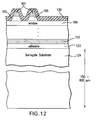
- FIG. 12 is a cross-sectional view of the solar cell of FIG. 11 after the next process step according to the present invention in which an ARC layer has been deposited;
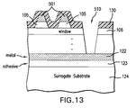
- FIG. 13 is a cross-sectional view of the solar cell of FIG. 12 after the next process step according to a first embodiment of the present invention in which a mesa etch isolation has been performed;
- FIG. 14A is a cross-sectional view of the solar cell of FIG. 13 after the next process step according to a first embodiment of the present invention in which the surrogate substrate has been thinned to a desired thickness;
- FIG. 14B is a cross-sectional view of the solar cell of FIG. 14A after the next process step according to a second embodiment of the present invention in which a coverglass is adhered to the solar cell;
- FIG. 15 is a cross-sectional view of a portion of a solar cell array which depicts the solar cell of FIG. 14A after the next process step according to an aspect of the present invention in which an electrical connection is made from a first cell to an adjacent solar cell;
- FIG. 16A is a cross-sectional view of the solar cell of FIG. 13 in a third embodiment of the present invention after the next process step of adhering a coverglass to the structure;
- FIG. 16B is a cross-sectional view of the solar cell of FIG. 16A after the next process step of removing the substrate.
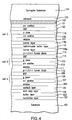
- FIG. 1 depicts the multijunction solar cell according to the present invention after formation of the three subcells A, B and C on a substrate. More particularly, there is shown a substrate 101, which may be either gallium arsenide (GaAs), germanium (Ge), or other suitable material.
- a suitable nucleation layer 102 is deposited on the substrate.
- a buffer layer 103, and an etch stop layer 104 are further deposited.
- a contact layer 105 is then deposited on layer 104, and a window layer 106 is deposited on the contact layer.
- the subcell A consisting of an n+ emitter layer 107 and a p-type base layer 108, is then deposited on the window layer 106.
- the multijunction solar cell structure could be formed by any suitable combination of group III to V elements listed in the periodic table subject to lattice constant and band gap requirements, wherein the group III includes boron (B), aluminum (Al), gallium (Ga), indium (In), and thallium (T).
- the group IV includes carbon (C), silicon (Si), germanium (Ge), and tin (Sn).
- the group V includes nitrogen (N), phosphorous (P), arsenic (As), antimony (Sb), and bismuth (Bi).
- the n+ emitter layer 107 is composed of InGa(Al)P
- p-type the base layer 108 is composed of InGA(Al)P.
- the Al term is parenthesis in the preceding formula means that A1 is an optional constituent, and in this instance may be used in an amount ranging from 0% to 30%.
- BSF back surface field
- the BSF layer 109 drives minority carriers from the region near the base/BSF interface surface to minimize the effect of recombination loss.
- a BSF layer 109 reduces recombination loss at the backside of the solar subcell A and thereby reduces the recombination in the base.
- BSF layer 109 On top of the BSF layer 109 is deposited a sequence of heavily doped p-type and n-type layers 110 which forms a tunnel diode which is a circuit element to connect subcell A to subcell B.
- a window layer 111 is deposited on top of the tunnel diode layers 110 .
- the window layer 111 used in the subcell B also operates to reduce the recombination loss.
- the window layer 111 also improves the passivation of the cell surface of the underlying junctions. It should be apparent to one skilled in the art, that additional layer(s) may be added or deleted in the cell structure without departing from the scope of the present invention.
- the layers of cell B are deposited: the emitter layer 112, and the p-type base layer 113. These layers are preferably composed of InGaP and In 0.015 GaAs respectively, although any other suitable materials consistent with lattice constant and band gap requirements may be used as well.
- a BSF layer 114 which performs the same function as the BSF layer 109.
- a p++/n++ tunnel diode 115 is deposited over the BSF layer 114 4 similar to the layers 110, again forming a circuit element to connect cell B to cell C.
- a barrier layer 116a preferably composed of InGa(Al)P, is deposited over the tunnel diode 115, to a thickness of about 1.0 micron. Such barrier layer is intended to prevent threading dislocations from propagating, either opposite to the direction of growth into the middle and top subcells B and C, or in the direction of growth into the bottom subcell A.
- a metamorphic layer 116 is deposited over the barrier layer 116a.
- Layer 116 is preferably a compositionally step-graded series of InGaAlAs layers with monotonically changing lattice constant that is intended to achieve a transition in lattice constant from subcell B to subcell C.
- the band gap of layer 116 is 1.5 eV consistent with a value slightly greater than the band gap of the middle subcell B.
- the step grade contains nine compositionally graded InGaP steps with each step layer having a thickness of 0.25 micron.
- the layer 116 is composed of nine layers of InGaAlAs, with monotonically changing lattice constant, or more particularly In x Ga 1-x AlAs with x chosen so that the band gap is constant at 1.50 eV.
- the number of layers, and the composition and lattice constant of each layer, may be appropriately adjusted depending on other growth or structural requirements.
- an optional second barrier layer 116b may be deposited over the InGaAlAs metamorphic layer 116.
- the second barrier layer 116b will typically have a slightly different composition than that of barrier layer 116a.
- a window layer 117 is deposited over the barrier layer 116b, this window layer operating to reduce the recombination loss in subcell "C". It should be apparent to one skilled in the art that additional layers may be added or deleted in the cell structure without departing from the scope of the present invention.
- the layers of cell C are deposited: the n+ emitter layer 118, and the p-type base layer 119. These layers are preferably composed of InGaP and GaInAs respectively, although another suitable materials consistent with lattice constant and band gap requirements may be used as well.
- a BSF layer 120 is deposited on top of the cell C, the BSF layer performing the same function as the BSF layers 109 and 114.
- a p+ contact layer 121 is deposited on the BSF layer 120.
- FIG. 2 is a cross-sectional view of the solar cell of FIG. 1 after the next process step in which a metal contact layer 122 is deposited over the p+ semiconductor contact layer 121.
- the metal is preferably the sequence of layers Ti/Au/Ag/Au.
- FIG. 3 is a cross-sectional view of the solar cell of FIG. 2 , after the next process step, in which an adhesive 123 is applied over the metal layer 122.
- the adhesive can be a temporary adhesive, or a permanent one.
- the permanent bond can even be due to the metal layer itself, for example in the case of eutectic or thermo compression bonding, to the substrate to be attached.
- FIG. 4 is a cross-sectional view of the solar cell of FIG. 3 , after the next process step, in which a surrogate substrate is attached, using the adhesion method detailed above.
- This surrogate substrate can be a temporary substrate, such as sapphire or glass, up to 1 mm in thickness. Or it can be a permanent substrate such as a silicon or germanium wafer, which can be electrically and/or thermally conductive. Using germanium as the substrate also allows thermal expansion matching between the III - V semiconductor layers of the solar cell and the substrate, thereby reducing warpage and cracking of the substrate/device layers.
- FIG. 5A is a cross-sectional view of the solar cell of FIG. 4 after the next process step in which the original substrate is removed by a sequence of lapping and/or etching steps in which the substrate 101, the buffer layer 103, and the etch stop layer 104, are removed.
- the etchant is growth substrate dependent.
- FIG. 5B is a cross-sectional view of the solar cell of FIG. 5A from the solar cell of FIG. 5A from the orientation with the surrogate substrate 124 being at the bottom of the Figure.
- FIG. 6A is a top plan view of a wafer in which the solar cells are implemented.
- each cell there are conductive grid lines 501 (more particularly shown in cross-section in FIG. 10 ) over the surface of the cell, an interconnecting bus line 502, and a contact pad 503 for making external electrical contact with the top of the cell.
- FIG. 6B is a bottom plan view of the wafer with four solar cells shown in FIG. 6A .
- the entire backside surface is covered with contact metal, representing layer 122
- FIG. 7 is a top plan view of the wafer of FIG. 6A after the next process step in which a channel 510 is etched around the periphery of each cell using phosphide and arsenide etchants to isolate each cell and form a contact pad area electrically connected to the bottom contact layer. The use of such a pad area will be subsequently described in connection with FIG. 15 .
- FIG. 8 is a simplified cross-sectional view of the solar cell of FIG. 5B depicting just a few of the top layers and lower layers over the surrogate substrate 124.
- FIG. 9 is a cross-sectional view of the solar cell of FIG. 8 after the next process step in which the etch stop layer 104 is removed by a HCl/H 2 O solution.
- FIG. 10 is a cross-sectional view of the solar cell of FIG. 9 after the next sequence of process steps in which a photoresist mask (not shown) is placed over the contact layer 105 to form the grid lines 501.
- the grid lines 501 are deposited via evaporation and lithographically patterned and deposited over the contact layer 105.
- the mask is lifted off to form the metal grid lines 501.
- FIG. 11 is a cross-sectional view of the solar cell of FIG. 10 after the next process step in which the grid lines are used as a mask to etch down the surface to the window layer 106 using a citric acid/peroxide etching mixture.
- FIG. 12 is a cross-sectional view of the solar cell of FIG. 11 after the next process step in which an antireflective (ARC) dielectric coating layer 130 is applied over the entire surface of the "top" (sunward) side of the wafer with the grid lines 501.
- ARC antireflective
- FIG. 13 is a cross-sectional view of the solar cell of FIG. 12 after the next process step according to the present invention in which a channel 510 or portion of the semiconductor structure is etched down to the metal layer 122 using phosphide and arsenide etchants leaving a mesa structure which constitutes the solar cell.
- the cross-section depicted in FIG. 13 is that as seen from the A-A plane shown in FIG. 7 .
- FIG. 14A a thin cell mounted on a thinned substrate
- FIG. 14B a thin cell mounted on a coverglass
- FIG. 16B a thin cell mounted on a coverglass
- FIG. 14A is a cross-sectional view of the solar cell of FIG. 13 after the next process step according to the present invention after the surrogate substrate 124 is thinned by a process of grinding, lapping or etching to a preferred thickness of about 2-6 mils.
- the right hand portion of the solar cell is then routed or cut to size, leaving the exposed metal layer 122 over the thinned substrate 124a which may be utilized to form a contact pad to the backside of the solar cell.
- the final structure of the solar cell is complete as depicted.
- the adhesive 123 and surrogate substrate 124a are conductive, so the bottom metal contact 122 is electrically coupled to the substrate 124a which then serves as the electrical contact to the backside of the solar cell.
- use of the layer 122 as a contact pad is unnecessary.
- FIG. 14B is a cross-sectional view of the solar cell of FIG. 14A after the next process step according to a second embodiment in which a coverglass is added to the present invention.
- An adhesive is applied over the ARC layer 130 and a coverglass attached to the adhesive.
- Such an embodiment of a thin solar cell mounted on a thinned substrate with a coverglass is typically used for solar cells intended for space applications, or other harsh environments.
- Contact may be made either to layer 122, or in another variant, the adhesive 123 and surrogate substrate 124a are conductive, so the bottom metal contact 122 is electrically coupled to the substrate 124a which serves as the electrical contact to the solar cell.
- FIG. 15 depicts the coupling of two adjacent solar cells Cell 1 and Cell 2 utilizing the metal layer 122 as a contact pad.
- the channel 510 in Cell 1 exposes a portion of the metal contact layer 122.
- a wire 512 is then welded or wire bonded between layer 122 on Cell 1 and the electrical contact pad 511 on Cell 2.
- Contact pad 511 makes electrical contact with the contact layer 105 of Cell 2 and thereby electrically couples to Cell 2. Such an electrical arrangement allows the cells to be connected in series.
- FIG. 16A is a cross-sectional view of the solar cell of FIG. 13 after the next process step according to a third embodiment of the present invention in which an adhesive is applied over the ARC layer 130 and a coverglass attached thereto.
- FIG. 16B is a cross-sectional view of the solar cell of FIG. 14A after the next process step according to the third embodiment of the present invention in which the surrogate substrate 124 is entirely removed by grinding, lapping, or etching, resulting in the finished device structure of a thin metamorphic solar cell mounted on a rigid coverglass.
- the subcells may alternatively be contacted by means of metal contacts to laterally conductive semiconductor layers between the subcells. Such arrangements may be used to form 3-terminal, 4-terminal, and in general, n-terminal devices.
- the subcells can be interconnected in circuits using these additional terminals such that most of the available photogenerated current density in each subcell can be used effectively, leading to high efficiency for the multijunction cell, notwithstanding that the photogenerated current densities are typically different in the various subcells.
- the present invention may utilize one or more homojunction cells or subcells, i.e., a cell or subcell in which the p-n junction is formed between a p-type semiconductor and an n-type semiconductor both of which have the same chemical composition and the same band gap, differing only in the dopant species and types.
- Subcell A with p-type and n-type InGaP is one example of a homojunction subcell.
- the present invention may utilize one or more heterojunction cells or subcells, i.e., a cell or subcell in which the p-n junction is formed between a p-type semiconductor and an n-type semiconductor having different chemical compositions of the semiconductor material in the n-type and n-type regions, and/or different band gap energies in the p-type regions, in addition to utilizing different dopant species and type in the p-type and n-type regions that form the p-n junction.
- heterojunction cells or subcells i.e., a cell or subcell in which the p-n junction is formed between a p-type semiconductor and an n-type semiconductor having different chemical compositions of the semiconductor material in the n-type and n-type regions, and/or different band gap energies in the p-type regions, in addition to utilizing different dopant species and type in the p-type and n-type regions that form the p-n junction.
- the composition of the window or BSF layers may utilize other semiconductor compounds, subject to lattice constant and bandgap requirements, and may include AlInP, AlAs, AlP, AlGaInP, AlGaAsP, AlGaInAs, AlGaInPAs, GaInP, GaInAs, GaInPAs, AlGaAs, AlInAs, AlInPAs, GaAsSb, AlAsSb, GaAlAsSb, AlInSb, GaInSb, AlGaInSb, AIN, GaN, InN, GaInN, AlGaInN, GaInNAs, AlGaInNAs, ZnSSe, CdSSe, and similar materials, and still fall within the spirit of the present invention.
Abstract
Description
- The present invention relates to the field of solar cell semiconductor devices, and particularly to integrated semiconductor structures mounted on a rigid carrier, such as inverted metamorphic solar cells.
- Photovoltaic cells, also called solar cells, are one of the most important new energy sources that have become available in the past several years. Considerable effort has gone into solar cell development. As a result, solar cells are currently being used in a number of commercial and consumer-oriented applications. While significant progress has been made in this area, the requirement for solar cells to meet the needs of more sophisticated applications has not kept pace with demand. Applications such as satellites used in data communications have dramatically increased the demand for solar cells with improved power and energy conversion characteristics.
- In satellite and other space related applications, the size, mass and cost of a satellite power system are dependent on the power and energy conversion efficiency of the solar cells used. Putting it another way, the size of the payload and the availability of on-board services are proportional to the amount of power provided. Thus, as the payloads become more sophisticated solar cells, which act as the power conversion devices for the on-board power systems, become increasingly more important
- Solar cells are often fabricated in vertical, multijunction structures, and disposed in horizontal arrays, with the individual solar cells connected together in a series. The shape and structure of an array, as well as the number of cells it contains, are determined in part by the desired output voltage and current.
- Occasionally, there is a need to reduce the thickness of wafers and devices. For example, in photodiodes, reducing the thickness of the substrate reduces the heat-conducting path, and enables the photodiode to handle more light at high speed. In space photovoltaics, the advantage to reducing the thickness is reduction of the payload weight at launch.
- Thinning the substrate means that some other means of support has to be given to the device layers, during processing, and in use. Also, any residual strain (from growth, thermal mismatch, etc.) in the device layers will present itself as curvature in the layers, which can be corrected by incorporating strain of the opposite sign in the support that's given to the layers, while still keeping if flexible for conformal attachment to a curved surface.
- Inverted metamorphic solar cell structures such as described in
U.S. Patent No. 6,951,819 and M.W. Wanlass et al., Lattice Mismatched Approaches for High Performance, III - V Photovoltaic Energy Converters (Conference Proceedings of the 31st IEEE Photovoltaic Specialists Conference, Jan. 3-7, 2005, IEEE Press, 2005) are important new solar cell structures and present one approach to thinning the substrate in a solar cell. However, the structures described in such prior art present a number of practical difficulties relating to the appropriate choice of materials and fabrication steps. - Prior to the present invention, the materials and fabrication steps disclosed in the prior art have not been adequate to produce a commercially viable, manufacturable, and energy efficient solar cell.
- It is an object of the present invention to provide an improved multijunction solar cell.
- It is an object of the invention to provide an improved inverted metamorphic solar cell.
- It is still another object of the invention to provide a method of manufacturing an inverted metamorphic solar cell as a thin film mounted on a thin substrate about 2 to 6 mils in thickness.
- It is still another object of the invention to provide a method of manufacturing an inverted metamorphic solar cell as a thin film mounted on a coverglass.
- It is still another object of the invention to provide an inverted metamorphic solar cell as a thin film mounted on a thin substrate about 2-6 mils in thickness.
- It is still another object of the invention to provide an inverted metamorphic solar cell as a thin film mounted solely on a coverglass.
- Additional objects, advantages, and novel features of the present invention will become apparent to those skilled in the art from this disclosure, including the following detailed description as well as by practice of the invention. While the invention is described below with reference to preferred embodiments, it should be understood that the invention is not limited thereto. Those of ordinary skill in the art having access to the teachings herein will recognize additional applications, modifications and embodiments in other fields, which are within the scope of the invention as disclosed and claimed herein and with respect to which the invention could be of utility.
- Briefly, and in general terms, the present invention provides a method of manufacturing a solar cell by providing a first substrate; depositing on the first substrate a sequence of layers of semiconductor material forming a solar cell; mounting a surrogate substrate on top of the sequence of layers; removing the first substrate; and thinning the surrogate substrate to a predetermined thickness.
- . In another aspect, the present invention provides a method of manufacturing a solar cell by providing a first substrate; depositing on the first substrate a sequence of layers of semiconductor material forming a solar cell; mounting a surrogate substrate on top of the sequence of layers; removing the first substrate; mounting the solar cell on a rigid coverglass; and removing the surrogate substrate.
- In another aspect, the present invention provides a multijunction solar cell including a first solar subcell having a first band gap; a second solar subcell disposed over the first subcell and having a second band gap smaller than the first band gap; a grading interlayer disposed over the second subcell and having a third band gap greater than the second band gap; a third solar subcell disposed over the interlayer that is lattice mis-matched with respect to the middle subcell and having a fourth band gap smaller than the second band gap; and a rigid coverglass supporting the first, second, and third solar subcells.
- In another aspect, the present invention provides a solar cell arrangement comprising:
- (i) a first solar cell including: a first solar subcell having a first band gap; a second solar subcell disposed over said first subcell and having a second band gap smaller than said first band gap; a grading interlayer disposed over said second subcell and having a third band gap greater than said second band gap; a third solar subcell disposed over said interlayer that is lattice-mis-matched with respect to said middle subcell and having a fourth band gap smaller than said second band gap; a metal contact layer disposed over said third solar subcell; and
- (ii) a second solar cell including: a first solar subcell having a first band gap; a second solar subcell disposed over said first subcell and having a second band gap smaller than said first band gap; a grading interlayer disposed over said second subcell and having a third band gap greater than said second band gap; a third solar subcell disposed over said interlayer that is lattice-mis-matched with respect to said middle subcell and having a fourth band gap smaller than said second band gap; a metal contact layer disposed over said third solar subcell; and
- (iii) a conductor bonded to said metal contact layer of said first solar cell for making electrical contact between said first solar cell and the first solar subcell of said second solar cell.
- These and other features and advantages of this invention will be better and more fully appreciated by reference to the following detailed description when considered in conjunction with the accompanying drawings, wherein:
-
FIG. 1 is an enlarged cross-sectional view of the solar cell according to the present invention at the end of the process steps of forming the layers of the solar cell; -
FIG. 2 is a cross-sectional view of the solar cell ofFIG. 1 after the next process step according to the present invention in which backside contact metallization is applied; -
FIG. 3 is a cross-sectional view of the solar cell ofFIG. 2 after the next process step according to the present invention in which an adhesive is applied; -
FIG. 4 is a cross-sectional view of the solar cell ofFIG. 3 after the next process step according to the present invention in which a surrogate substrate is attached; -
FIG. 5A is a cross-sectional view of the solar cell ofFIG. 4 after the next process step according to the present invention in which the original substrate is removed; -
FIG. 5B is a cross-sectional view of the solar cell ofFIG. 5A with the surrogate substrate depicted at the bottom of the Figure; -
FIG. 6A is a top plan view of a wafer in which the solar cells according to the present invention are fabricated; -
FIG. 6B is a bottom plan view of a wafer in which the solar cells according to the present invention are fabricated; -
FIG. 7 is a top plan view of the wafer ofFIG. 6B after the next process step according to the present invention; -
FIG. 8 is a cross-sectional view of the solar cell ofFIG. 5B after the next process step according to the present invention in which the buffer layer has been etched off; -
FIG. 9 is a cross-sectional view of the solar cell ofFIG. 8 after the next process step according to the present invention; -
FIG. 10 is a cross-sectional view of the solar cell ofFIG. 9 after the next process step according to the present invention; -
FIG. 11 is a cross-sectional view of the solar cell ofFIG. 10 after the next process step according to the present invention; -
FIG. 12 is a cross-sectional view of the solar cell ofFIG. 11 after the next process step according to the present invention in which an ARC layer has been deposited; -
FIG. 13 is a cross-sectional view of the solar cell ofFIG. 12 after the next process step according to a first embodiment of the present invention in which a mesa etch isolation has been performed; -
FIG. 14A is a cross-sectional view of the solar cell ofFIG. 13 after the next process step according to a first embodiment of the present invention in which the surrogate substrate has been thinned to a desired thickness; -
FIG. 14B is a cross-sectional view of the solar cell ofFIG. 14A after the next process step according to a second embodiment of the present invention in which a coverglass is adhered to the solar cell; -
FIG. 15 is a cross-sectional view of a portion of a solar cell array which depicts the solar cell ofFIG. 14A after the next process step according to an aspect of the present invention in which an electrical connection is made from a first cell to an adjacent solar cell; -
FIG. 16A is a cross-sectional view of the solar cell ofFIG. 13 in a third embodiment of the present invention after the next process step of adhering a coverglass to the structure; and -
FIG. 16B is a cross-sectional view of the solar cell ofFIG. 16A after the next process step of removing the substrate. - Details of the present invention will now be described including exemplary aspects and embodiments thereof. Referring to the drawings and the following description, like reference numbers are used to identify like or functionally similar elements, and are intended to illustrate major features of exemplary embodiments in a highly simplified diagrammatic manner. Moreover, the drawings are not intended to depict every feature of the actual embodiment nor the relative dimensions of the depicted elements, and are not drawn to scale.
-
FIG. 1 depicts the multijunction solar cell according to the present invention after formation of the three subcells A, B and C on a substrate. More particularly, there is shown asubstrate 101, which may be either gallium arsenide (GaAs), germanium (Ge), or other suitable material. In the case of a Ge substrate, asuitable nucleation layer 102 is deposited on the substrate. On the substrate, or over thenucleation layer 102, abuffer layer 103, and anetch stop layer 104 are further deposited. Acontact layer 105 is then deposited onlayer 104, and awindow layer 106 is deposited on the contact layer. The subcell A, consisting of ann+ emitter layer 107 and a p-type base layer 108, is then deposited on thewindow layer 106. - It should be noted that the multijunction solar cell structure could be formed by any suitable combination of group III to V elements listed in the periodic table subject to lattice constant and band gap requirements, wherein the group III includes boron (B), aluminum (Al), gallium (Ga), indium (In), and thallium (T). The group IV includes carbon (C), silicon (Si), germanium (Ge), and tin (Sn). The group V includes nitrogen (N), phosphorous (P), arsenic (As), antimony (Sb), and bismuth (Bi).
- In the preferred embodiment, the
n+ emitter layer 107 is composed of InGa(Al)P And p-type thebase layer 108 is composed of InGA(Al)P. The Al term is parenthesis in the preceding formula means that A1 is an optional constituent, and in this instance may be used in an amount ranging from 0% to 30%. - On top of the
base layer 108 is deposited a back surface field ("BSF")layer 109 used to reduce recombination loss. - The
BSF layer 109 drives minority carriers from the region near the base/BSF interface surface to minimize the effect of recombination loss. In other words, aBSF layer 109 reduces recombination loss at the backside of the solar subcell A and thereby reduces the recombination in the base. - On top of the
BSF layer 109 is deposited a sequence of heavily doped p-type and n-type layers 110 which forms a tunnel diode which is a circuit element to connect subcell A to subcell B. - On top of the tunnel diode layers 110 a
window layer 111 is deposited. Thewindow layer 111 used in the subcell B also operates to reduce the recombination loss. Thewindow layer 111 also improves the passivation of the cell surface of the underlying junctions.
It should be apparent to one skilled in the art, that additional layer(s) may be added or deleted in the cell structure without departing from the scope of the present invention. - On top of the
window layer 111 the layers of cell B are deposited: theemitter layer 112, and the p-type base layer 113. These layers are preferably composed of InGaP and In0.015GaAs respectively, although any other suitable materials consistent with lattice constant and band gap requirements may be used as well. - On top of the cell B is deposited a
BSF layer 114 which performs the same function as theBSF layer 109. A p++/n++ tunnel diode 115 is deposited over theBSF layer 114 4 similar to thelayers 110, again forming a circuit element to connect cell B to cell C. - A
barrier layer 116a, preferably composed of InGa(Al)P, is deposited over thetunnel diode 115, to a thickness of about 1.0 micron. Such barrier layer is intended to prevent threading dislocations from propagating, either opposite to the direction of growth into the middle and top subcells B and C, or in the direction of growth into the bottom subcell A. - A
metamorphic layer 116 is deposited over thebarrier layer 116a.Layer 116 is preferably a compositionally step-graded series of InGaAlAs layers with monotonically changing lattice constant that is intended to achieve a transition in lattice constant from subcell B to subcell C. The band gap oflayer 116 is 1.5 eV consistent with a value slightly greater than the band gap of the middle subcell B. - In one embodiment, as suggested in the Wanless et al. paper, the step grade contains nine compositionally graded InGaP steps with each step layer having a thickness of 0.25 micron. In the preferred embodiment, the
layer 116 is composed of nine layers of InGaAlAs, with monotonically changing lattice constant, or more particularly InxGa1-x AlAs with x chosen so that the band gap is constant at 1.50 eV. The number of layers, and the composition and lattice constant of each layer, may be appropriately adjusted depending on other growth or structural requirements. - In another embodiment of the present invention, an optional
second barrier layer 116b may be deposited over the InGaAlAsmetamorphic layer 116. Thesecond barrier layer 116b will typically have a slightly different composition than that ofbarrier layer 116a. - A
window layer 117 is deposited over thebarrier layer 116b, this window layer operating to reduce the recombination loss in subcell "C". It should be apparent to one skilled in the art that additional layers may be added or deleted in the cell structure without departing from the scope of the present invention. - On top of the
window layer 117, the layers of cell C are deposited: then+ emitter layer 118, and the p-type base layer 119. These layers are preferably composed of InGaP and GaInAs respectively, although another suitable materials consistent with lattice constant and band gap requirements may be used as well. - A
BSF layer 120 is deposited on top of the cell C, the BSF layer performing the same function as the BSF layers 109 and 114. - Finally a
p+ contact layer 121 is deposited on theBSF layer 120. - It should be apparent to one skilled in the art, that additional layer(s) may be added or deleted in the cell structure without departing from the scope of the present invention.
-
FIG. 2 is a cross-sectional view of the solar cell ofFIG. 1 after the next process step in which ametal contact layer 122 is deposited over the p+semiconductor contact layer 121. The metal is preferably the sequence of layers Ti/Au/Ag/Au. -
FIG. 3 is a cross-sectional view of the solar cell ofFIG. 2 , after the next process step, in which an adhesive 123 is applied over themetal layer 122. The adhesive can be a temporary adhesive, or a permanent one. The permanent bond can even be due to the metal layer itself, for example in the case of eutectic or thermo compression bonding, to the substrate to be attached. -
FIG. 4 is a cross-sectional view of the solar cell ofFIG. 3 , after the next process step, in which a surrogate substrate is attached, using the adhesion method detailed above. This surrogate substrate can be a temporary substrate, such as sapphire or glass, up to 1 mm in thickness. Or it can be a permanent substrate such as a silicon or germanium wafer, which can be electrically and/or thermally conductive. Using germanium as the substrate also allows thermal expansion matching between the III - V semiconductor layers of the solar cell and the substrate, thereby reducing warpage and cracking of the substrate/device layers. -
FIG. 5A is a cross-sectional view of the solar cell ofFIG. 4 after the next process step in which the original substrate is removed by a sequence of lapping and/or etching steps in which thesubstrate 101, thebuffer layer 103, and theetch stop layer 104, are removed. The etchant is growth substrate dependent. -
FIG. 5B is a cross-sectional view of the solar cell ofFIG. 5A from the solar cell ofFIG. 5A from the orientation with thesurrogate substrate 124 being at the bottom of the Figure. -
FIG. 6A is a top plan view of a wafer in which the solar cells are implemented. - As more particularly illustrated in
Cell 1, in each cell there are conductive grid lines 501 (more particularly shown in cross-section inFIG. 10 ) over the surface of the cell, an interconnectingbus line 502, and acontact pad 503 for making external electrical contact with the top of the cell. -
FIG. 6B is a bottom plan view of the wafer with four solar cells shown inFIG. 6A . In the embodiment depicted, the entire backside surface is covered with contact metal, representinglayer 122 -
FIG. 7 is a top plan view of the wafer ofFIG. 6A after the next process step in which achannel 510 is etched around the periphery of each cell using phosphide and arsenide etchants to isolate each cell and form a contact pad area electrically connected to the bottom contact layer. The use of such a pad area will be subsequently described in connection withFIG. 15 . -
FIG. 8 is a simplified cross-sectional view of the solar cell ofFIG. 5B depicting just a few of the top layers and lower layers over thesurrogate substrate 124. -
FIG. 9 is a cross-sectional view of the solar cell ofFIG. 8 after the next process step in which theetch stop layer 104 is removed by a HCl/H2O solution. -
FIG. 10 is a cross-sectional view of the solar cell ofFIG. 9 after the next sequence of process steps in which a photoresist mask (not shown) is placed over thecontact layer 105 to form the grid lines 501. The grid lines 501 are deposited via evaporation and lithographically patterned and deposited over thecontact layer 105. The mask is lifted off to form the metal grid lines 501. -
FIG. 11 is a cross-sectional view of the solar cell ofFIG. 10 after the next process step in which the grid lines are used as a mask to etch down the surface to thewindow layer 106 using a citric acid/peroxide etching mixture. -
FIG. 12 is a cross-sectional view of the solar cell ofFIG. 11 after the next process step in which an antireflective (ARC)dielectric coating layer 130 is applied over the entire surface of the "top" (sunward) side of the wafer with the grid lines 501. -
FIG. 13 is a cross-sectional view of the solar cell ofFIG. 12 after the next process step according to the present invention in which achannel 510 or portion of the semiconductor structure is etched down to themetal layer 122 using phosphide and arsenide etchants leaving a mesa structure which constitutes the solar cell. The cross-section depicted inFIG. 13 is that as seen from the A-A plane shown inFIG. 7 . - The next Figures will depict various embodiments of the invention of a thin inverted metamorphic solar cell on a rigid support, including (i) a thin cell mounted on a thinned substrate (
Fig. 14A ), (ii) a thin cell mounted on a thinned substrate with a coverglass (FIG. 14B ), and (iii) a thin cell mounted on a coverglass (FIG. 16B ). -
FIG. 14A is a cross-sectional view of the solar cell ofFIG. 13 after the next process step according to the present invention after thesurrogate substrate 124 is thinned by a process of grinding, lapping or etching to a preferred thickness of about 2-6 mils. The right hand portion of the solar cell is then routed or cut to size, leaving the exposedmetal layer 122 over the thinnedsubstrate 124a which may be utilized to form a contact pad to the backside of the solar cell. In a first embodiment of the present invention, such as solar cells for use in terrestrial applications, the final structure of the solar cell is complete as depicted. In a variant of this first embodiment, the adhesive 123 andsurrogate substrate 124a are conductive, so thebottom metal contact 122 is electrically coupled to thesubstrate 124a which then serves as the electrical contact to the backside of the solar cell. In such a variant, use of thelayer 122 as a contact pad is unnecessary. -
FIG. 14B is a cross-sectional view of the solar cell ofFIG. 14A after the next process step according to a second embodiment in which a coverglass is added to the present invention. An adhesive is applied over theARC layer 130 and a coverglass attached to the adhesive. Such an embodiment of a thin solar cell mounted on a thinned substrate with a coverglass is typically used for solar cells intended for space applications, or other harsh environments. Contact may be made either tolayer 122, or in another variant, the adhesive 123 andsurrogate substrate 124a are conductive, so thebottom metal contact 122 is electrically coupled to thesubstrate 124a which serves as the electrical contact to the solar cell. -
FIG. 15 depicts the coupling of two adjacentsolar cells Cell 1 andCell 2 utilizing themetal layer 122 as a contact pad. Thechannel 510 inCell 1 exposes a portion of themetal contact layer 122. Awire 512 is then welded or wire bonded betweenlayer 122 onCell 1 and theelectrical contact pad 511 onCell 2.Contact pad 511 makes electrical contact with thecontact layer 105 ofCell 2 and thereby electrically couples toCell 2. Such an electrical arrangement allows the cells to be connected in series. -
FIG. 16A is a cross-sectional view of the solar cell ofFIG. 13 after the next process step according to a third embodiment of the present invention in which an adhesive is applied over theARC layer 130 and a coverglass attached thereto. -
FIG. 16B is a cross-sectional view of the solar cell ofFIG. 14A after the next process step according to the third embodiment of the present invention in which thesurrogate substrate 124 is entirely removed by grinding, lapping, or etching, resulting in the finished device structure of a thin metamorphic solar cell mounted on a rigid coverglass. - It will be understood that each of the elements described above, or two or more together, also may find a useful application in other types of constructions differing from the types of constructions differing from the types described above.
- Although the preferred embodiment of the present invention utilizes a vertical stack of subcells with top and bottom electrical contacts, the subcells may alternatively be contacted by means of metal contacts to laterally conductive semiconductor layers between the subcells. Such arrangements may be used to form 3-terminal, 4-terminal, and in general, n-terminal devices. The subcells can be interconnected in circuits using these additional terminals such that most of the available photogenerated current density in each subcell can be used effectively, leading to high efficiency for the multijunction cell, notwithstanding that the photogenerated current densities are typically different in the various subcells.
- As noted above, the present invention may utilize one or more homojunction cells or subcells, i.e., a cell or subcell in which the p-n junction is formed between a p-type semiconductor and an n-type semiconductor both of which have the same chemical composition and the same band gap, differing only in the dopant species and types. Subcell A, with p-type and n-type InGaP is one example of a homojunction subcell. Alternatively, the present invention may utilize one or more heterojunction cells or subcells, i.e., a cell or subcell in which the p-n junction is formed between a p-type semiconductor and an n-type semiconductor having different chemical compositions of the semiconductor material in the n-type and n-type regions, and/or different band gap energies in the p-type regions, in addition to utilizing different dopant species and type in the p-type and n-type regions that form the p-n junction.
- The composition of the window or BSF layers may utilize other semiconductor compounds, subject to lattice constant and bandgap requirements, and may include AlInP, AlAs, AlP, AlGaInP, AlGaAsP, AlGaInAs, AlGaInPAs, GaInP, GaInAs, GaInPAs, AlGaAs, AlInAs, AlInPAs, GaAsSb, AlAsSb, GaAlAsSb, AlInSb, GaInSb, AlGaInSb, AIN, GaN, InN, GaInN, AlGaInN, GaInNAs, AlGaInNAs, ZnSSe, CdSSe, and similar materials, and still fall within the spirit of the present invention.
Claims (24)
- A method of manufacturing a solar cell comprising:providing a first substrate;depositing on a first substrate a sequence of layers of semiconductor material forming a solar cell;mounting a surrogate substrate on top of the sequence of layers;removing the first substrate; andthinning the surrogate substrate to a predetermined thickness.
- A method as defined in claim 1, wherein the sequence of layers of semiconductor material forms a triple junction solar cell, including first, second and third solar subcells.
- A method as defined in claim 1, wherein the mounting step includes adhering the solar cell to the surrogate substrate.
- A method as defined in claim 3, wherein the surrogate substrate is a sapphire wafer.
- A method as defined in claim 3, wherein the thinning of said surrogate substrate is done by grinding, lapping, or etching.
- A method as defined in claim 5, further comprising depositing a metal contact layer over said sequence of semiconductor layers, and mounting said surrogate substrate on top of said metal contact layer.
- A method as defined in claim 6, further comprising etching an opening through said layers of semiconductor material to the top of said metal contact layer.
- A method as defined in claim 7, further comprising welding an electrical conductor to said metal contact layer to form an electrical contact to said solar cell.
- A method as defined in claim 8, wherein said electrical conductor makes an electrical connection to an adjacent solar cell.
- A method as defined in claim 3, wherein said surrogate substrate is electrically conductive and said substrate forms an electrical contact to said solar cell.
- A method as defined in claim 1, further comprising attaching said solar cell to a glass supporting member.
- A method as defined in claim 1, wherein said step of depositing a sequence of layers of semiconductor material includes forming a first solar subcell on said substrate having a first band gap; forming a second solar subcell over said first subcell having a second band gap smaller than said first band gap; forming a grading interlayer over said second subcell having a third band gap larger than said second band gap; forming a third solar subcell having a fourth band gap smaller than said second band gap such that said third subcell is lattice mis-matched with respect to said second subcell.
- A method of manufacturing a solar cell as defined in claim 1, wherein said first substrate is composed of GaAs.
- A method of manufacturing a solar cell as defined in claim 2, wherein said first solar subcell is composed of an InGa(Al)P emitter region and an InGa(Al)P base region.
- A method as defined in claim 2, wherein said second solar subcell is composed of an InGaP emitter region and a GaAs base region.
- A method as defined in claim 2, wherein said third solar subcell is composed of InGaAs.
- A method as defined in claim 1, further comprising:mounting the solar cell on rigid coverglass.
- A method as defined in claim 1, wherein the thinning of said surrogate substrate removes the entire surrogate substrate.
- A multijunction solar cell comprising:a first solar subcell having a first band gap;a second solar subcell disposed over said first subcell and having a second band gap smaller than said first band gap:a grading interlayer disposed over said second subcell and having a third band gap greater than said second band gap;a third solar subcell disposed over said interlayer that is lattice mis-matched with respect to said middle subcell and having a fourth band gap smaller than said second band gap; anda rigid coverglass supporting said first, second and third solar subcells.
- A multijunction solar cell as defined in claim 28, wherein the first solar subcell is the top cell and is composed of InGa(Al)P.
- A multijunction solar cell as defined in claim 19, wherein the second solar subcell is composed of InGaP and In0.015GaAs.
- A multijunction solar cell as defined in claim 19, wherein the grading interlayer is composed of InGaAIAs.
- A multijunction solar cell as defined in claim 19, wherein the third solar subcell is composed of In0.30GaAs.
- A multijunction solar cell as defined in claim 19, wherein the grading interlayer is composed of InxGa1-xAlAs with x such that the band gap remains constant at 1.50 eV.
Applications Claiming Priority (1)
| Application Number | Priority Date | Filing Date | Title |
|---|---|---|---|
| US11/860,142 US20090078308A1 (en) | 2007-09-24 | 2007-09-24 | Thin Inverted Metamorphic Multijunction Solar Cells with Rigid Support |
Publications (2)
| Publication Number | Publication Date |
|---|---|
| EP2040309A2 true EP2040309A2 (en) | 2009-03-25 |
| EP2040309A3 EP2040309A3 (en) | 2010-02-24 |
Family
ID=40254468
Family Applications (1)
| Application Number | Title | Priority Date | Filing Date |
|---|---|---|---|
| EP08013466A Withdrawn EP2040309A3 (en) | 2007-09-24 | 2008-07-25 | Thin inverted metamorphic multijunction solar cells with rigid support |
Country Status (5)
| Country | Link |
|---|---|
| US (1) | US20090078308A1 (en) |
| EP (1) | EP2040309A3 (en) |
| JP (1) | JP2009076921A (en) |
| CN (1) | CN101399296B (en) |
| TW (1) | TW200917512A (en) |
Families Citing this family (73)
| Publication number | Priority date | Publication date | Assignee | Title |
|---|---|---|---|---|
| US20060162768A1 (en) | 2002-05-21 | 2006-07-27 | Wanlass Mark W | Low bandgap, monolithic, multi-bandgap, optoelectronic devices |
| US8067687B2 (en) | 2002-05-21 | 2011-11-29 | Alliance For Sustainable Energy, Llc | High-efficiency, monolithic, multi-bandgap, tandem photovoltaic energy converters |
| US8772628B2 (en) | 2004-12-30 | 2014-07-08 | Alliance For Sustainable Energy, Llc | High performance, high bandgap, lattice-mismatched, GaInP solar cells |
| US20100229926A1 (en) | 2009-03-10 | 2010-09-16 | Emcore Solar Power, Inc. | Four Junction Inverted Metamorphic Multijunction Solar Cell with a Single Metamorphic Layer |
| US9634172B1 (en) | 2007-09-24 | 2017-04-25 | Solaero Technologies Corp. | Inverted metamorphic multijunction solar cell with multiple metamorphic layers |
| US20090078310A1 (en) * | 2007-09-24 | 2009-03-26 | Emcore Corporation | Heterojunction Subcells In Inverted Metamorphic Multijunction Solar Cells |
| US20100229913A1 (en) * | 2009-01-29 | 2010-09-16 | Emcore Solar Power, Inc. | Contact Layout and String Interconnection of Inverted Metamorphic Multijunction Solar Cells |
| US20100122724A1 (en) | 2008-11-14 | 2010-05-20 | Emcore Solar Power, Inc. | Four Junction Inverted Metamorphic Multijunction Solar Cell with Two Metamorphic Layers |
| US10170656B2 (en) | 2009-03-10 | 2019-01-01 | Solaero Technologies Corp. | Inverted metamorphic multijunction solar cell with a single metamorphic layer |
| US10381501B2 (en) | 2006-06-02 | 2019-08-13 | Solaero Technologies Corp. | Inverted metamorphic multijunction solar cell with multiple metamorphic layers |
| US20090078309A1 (en) * | 2007-09-24 | 2009-03-26 | Emcore Corporation | Barrier Layers In Inverted Metamorphic Multijunction Solar Cells |
| US9117966B2 (en) | 2007-09-24 | 2015-08-25 | Solaero Technologies Corp. | Inverted metamorphic multijunction solar cell with two metamorphic layers and homojunction top cell |
| US20100203730A1 (en) * | 2009-02-09 | 2010-08-12 | Emcore Solar Power, Inc. | Epitaxial Lift Off in Inverted Metamorphic Multijunction Solar Cells |
| US8686282B2 (en) | 2006-08-07 | 2014-04-01 | Emcore Solar Power, Inc. | Solar power system for space vehicles or satellites using inverted metamorphic multijunction solar cells |
| US20100047959A1 (en) * | 2006-08-07 | 2010-02-25 | Emcore Solar Power, Inc. | Epitaxial Lift Off on Film Mounted Inverted Metamorphic Multijunction Solar Cells |
| US20080029151A1 (en) * | 2006-08-07 | 2008-02-07 | Mcglynn Daniel | Terrestrial solar power system using III-V semiconductor solar cells |
| US20100093127A1 (en) * | 2006-12-27 | 2010-04-15 | Emcore Solar Power, Inc. | Inverted Metamorphic Multijunction Solar Cell Mounted on Metallized Flexible Film |
| US20110041898A1 (en) * | 2009-08-19 | 2011-02-24 | Emcore Solar Power, Inc. | Back Metal Layers in Inverted Metamorphic Multijunction Solar Cells |
| US7825328B2 (en) * | 2007-04-09 | 2010-11-02 | Taiwan Semiconductor Manufacturing Company, Ltd. | Nitride-based multi-junction solar cell modules and methods for making the same |
| US20100233838A1 (en) * | 2009-03-10 | 2010-09-16 | Emcore Solar Power, Inc. | Mounting of Solar Cells on a Flexible Substrate |
| US8895342B2 (en) | 2007-09-24 | 2014-11-25 | Emcore Solar Power, Inc. | Heterojunction subcells in inverted metamorphic multijunction solar cells |
| US10381505B2 (en) | 2007-09-24 | 2019-08-13 | Solaero Technologies Corp. | Inverted metamorphic multijunction solar cells including metamorphic layers |
| US20090155952A1 (en) * | 2007-12-13 | 2009-06-18 | Emcore Corporation | Exponentially Doped Layers In Inverted Metamorphic Multijunction Solar Cells |
| US20090272430A1 (en) * | 2008-04-30 | 2009-11-05 | Emcore Solar Power, Inc. | Refractive Index Matching in Inverted Metamorphic Multijunction Solar Cells |
| US20100012175A1 (en) | 2008-07-16 | 2010-01-21 | Emcore Solar Power, Inc. | Ohmic n-contact formed at low temperature in inverted metamorphic multijunction solar cells |
| US20090272438A1 (en) * | 2008-05-05 | 2009-11-05 | Emcore Corporation | Strain Balanced Multiple Quantum Well Subcell In Inverted Metamorphic Multijunction Solar Cell |
| US9287438B1 (en) * | 2008-07-16 | 2016-03-15 | Solaero Technologies Corp. | Method for forming ohmic N-contacts at low temperature in inverted metamorphic multijunction solar cells with contaminant isolation |
| US20100012174A1 (en) * | 2008-07-16 | 2010-01-21 | Emcore Corporation | High band gap contact layer in inverted metamorphic multijunction solar cells |
| US8263853B2 (en) * | 2008-08-07 | 2012-09-11 | Emcore Solar Power, Inc. | Wafer level interconnection of inverted metamorphic multijunction solar cells |
| US7741146B2 (en) | 2008-08-12 | 2010-06-22 | Emcore Solar Power, Inc. | Demounting of inverted metamorphic multijunction solar cells |
| US20100065105A1 (en) * | 2008-09-12 | 2010-03-18 | Francois Andre Koran | Thin Film Photovoltaic Module Having a Contoured Substrate |
| US8236600B2 (en) * | 2008-11-10 | 2012-08-07 | Emcore Solar Power, Inc. | Joining method for preparing an inverted metamorphic multijunction solar cell |
| US20100122764A1 (en) * | 2008-11-14 | 2010-05-20 | Emcore Solar Power, Inc. | Surrogate Substrates for Inverted Metamorphic Multijunction Solar Cells |
| US20100139755A1 (en) * | 2008-12-09 | 2010-06-10 | Twin Creeks Technologies, Inc. | Front connected photovoltaic assembly and associated methods |
| US10541349B1 (en) | 2008-12-17 | 2020-01-21 | Solaero Technologies Corp. | Methods of forming inverted multijunction solar cells with distributed Bragg reflector |
| US9018521B1 (en) | 2008-12-17 | 2015-04-28 | Solaero Technologies Corp. | Inverted metamorphic multijunction solar cell with DBR layer adjacent to the top subcell |
| US7960201B2 (en) * | 2009-01-29 | 2011-06-14 | Emcore Solar Power, Inc. | String interconnection and fabrication of inverted metamorphic multijunction solar cells |
| US8778199B2 (en) | 2009-02-09 | 2014-07-15 | Emoore Solar Power, Inc. | Epitaxial lift off in inverted metamorphic multijunction solar cells |
| US20100206365A1 (en) * | 2009-02-19 | 2010-08-19 | Emcore Solar Power, Inc. | Inverted Metamorphic Multijunction Solar Cells on Low Density Carriers |
| US20100229933A1 (en) * | 2009-03-10 | 2010-09-16 | Emcore Solar Power, Inc. | Inverted Metamorphic Multijunction Solar Cells with a Supporting Coating |
| US9018519B1 (en) | 2009-03-10 | 2015-04-28 | Solaero Technologies Corp. | Inverted metamorphic multijunction solar cells having a permanent supporting substrate |
| US8283558B2 (en) * | 2009-03-27 | 2012-10-09 | The Boeing Company | Solar cell assembly with combined handle substrate and bypass diode and method |
| US20100282288A1 (en) * | 2009-05-06 | 2010-11-11 | Emcore Solar Power, Inc. | Solar Cell Interconnection on a Flexible Substrate |
| JP5360818B2 (en) * | 2009-06-05 | 2013-12-04 | 国立大学法人福井大学 | Tandem solar cell and production method thereof |
| US8263856B2 (en) * | 2009-08-07 | 2012-09-11 | Emcore Solar Power, Inc. | Inverted metamorphic multijunction solar cells with back contacts |
| US20110073887A1 (en) * | 2009-09-25 | 2011-03-31 | Alliance For Sustainable Energy, Llc | Optoelectronic devices having a direct-band-gap base and an indirect-band-gap emitter |
| TWI411116B (en) * | 2009-11-17 | 2013-10-01 | Epistar Corp | A high efficiency solar cell |
| JP5215284B2 (en) | 2009-12-25 | 2013-06-19 | シャープ株式会社 | Multi-junction compound semiconductor solar cell |
| US8187907B1 (en) | 2010-05-07 | 2012-05-29 | Emcore Solar Power, Inc. | Solder structures for fabrication of inverted metamorphic multijunction solar cells |
| US8878048B2 (en) * | 2010-05-17 | 2014-11-04 | The Boeing Company | Solar cell structure including a silicon carrier containing a by-pass diode |
| CN101976690A (en) * | 2010-08-23 | 2011-02-16 | 北京工业大学 | Four-junction semiconductor solar photovoltaic cell chip |
| CN101980367B (en) * | 2010-08-23 | 2013-01-23 | 广东瑞德兴阳光伏科技有限公司 | Four-junction solar photovoltaic cell chip for compound semiconductor |
| CN101964398A (en) * | 2010-10-11 | 2011-02-02 | 福建钧石能源有限公司 | Flexible thin film solar cell and manufacturing method thereof |
| WO2012051324A1 (en) | 2010-10-12 | 2012-04-19 | Alliance For Sustainable Energy, Llc | High bandgap iii-v alloys for high efficiency optoelectronics |
| JP2014512699A (en) * | 2011-04-29 | 2014-05-22 | アンバーウェーブ, インコーポレイテッド | Thin film solder joint |
| US9184332B2 (en) * | 2011-07-05 | 2015-11-10 | The Boeing Company | Inverted metamorphic multi-junction (IMM) solar cell and associated fabrication method |
| TWI497569B (en) * | 2012-04-18 | 2015-08-21 | Univ Nat Central | Used in the integration of compound semiconductor components in silicon or germanium substrate crystal structure |
| US10153388B1 (en) | 2013-03-15 | 2018-12-11 | Solaero Technologies Corp. | Emissivity coating for space solar cell arrays |
| US9590131B2 (en) | 2013-03-27 | 2017-03-07 | Alliance For Sustainable Energy, Llc | Systems and methods for advanced ultra-high-performance InP solar cells |
| JP2015050367A (en) * | 2013-09-03 | 2015-03-16 | 日本電信電話株式会社 | Solar battery |
| US9758261B1 (en) | 2015-01-15 | 2017-09-12 | Solaero Technologies Corp. | Inverted metamorphic multijunction solar cell with lightweight laminate substrate |
| US9935209B2 (en) | 2016-01-28 | 2018-04-03 | Solaero Technologies Corp. | Multijunction metamorphic solar cell for space applications |
| US10270000B2 (en) | 2015-10-19 | 2019-04-23 | Solaero Technologies Corp. | Multijunction metamorphic solar cell assembly for space applications |
| US10403778B2 (en) * | 2015-10-19 | 2019-09-03 | Solaero Technologies Corp. | Multijunction solar cell assembly for space applications |
| US10361330B2 (en) | 2015-10-19 | 2019-07-23 | Solaero Technologies Corp. | Multijunction solar cell assemblies for space applications |
| US10256359B2 (en) | 2015-10-19 | 2019-04-09 | Solaero Technologies Corp. | Lattice matched multijunction solar cell assemblies for space applications |
| US9985161B2 (en) | 2016-08-26 | 2018-05-29 | Solaero Technologies Corp. | Multijunction metamorphic solar cell for space applications |
| US10263134B1 (en) | 2016-05-25 | 2019-04-16 | Solaero Technologies Corp. | Multijunction solar cells having an indirect high band gap semiconductor emitter layer in the upper solar subcell |
| US10636926B1 (en) | 2016-12-12 | 2020-04-28 | Solaero Technologies Corp. | Distributed BRAGG reflector structures in multijunction solar cells |
| US20190181289A1 (en) | 2017-12-11 | 2019-06-13 | Solaero Technologies Corp. | Multijunction solar cells |
| US11011660B1 (en) * | 2018-07-17 | 2021-05-18 | Solaero Technologies Corp. | Inverted metamorphic multijunction solar cell |
| CN110246923A (en) * | 2019-06-29 | 2019-09-17 | 深圳黑晶光电科技有限公司 | A kind of tandem type perovskite/homojunction silicon lamination solar cell and preparation method thereof |
| CN112885921B (en) * | 2021-01-14 | 2022-10-25 | 常州信息职业技术学院 | GaInP/GaAs/AlGaSb triple-junction cascade solar cell and preparation method thereof |
Citations (9)
| Publication number | Priority date | Publication date | Assignee | Title |
|---|---|---|---|---|
| US4612408A (en) * | 1984-10-22 | 1986-09-16 | Sera Solar Corporation | Electrically isolated semiconductor integrated photodiode circuits and method |
| EP1109230A2 (en) * | 1999-12-02 | 2001-06-20 | The Boeing Company | Multijunction photovoltaic cell using a silicon or silicon-germanium substrate |
| WO2005015638A1 (en) * | 2003-07-22 | 2005-02-17 | Akzo Nobel N.V. | Process for manufacturing a solar cell foil using a temporary substrate |
| US20060021565A1 (en) * | 2004-07-30 | 2006-02-02 | Aonex Technologies, Inc. | GaInP / GaAs / Si triple junction solar cell enabled by wafer bonding and layer transfer |
| FR2878076A1 (en) * | 2004-11-17 | 2006-05-19 | St Microelectronics Sa | SLIMMING A SEMICONDUCTOR WAFER |
| US20060112986A1 (en) * | 2004-10-21 | 2006-06-01 | Aonex Technologies, Inc. | Multi-junction solar cells and methods of making same using layer transfer and bonding techniques |
| US20060185582A1 (en) * | 2005-02-18 | 2006-08-24 | Atwater Harry A Jr | High efficiency solar cells utilizing wafer bonding and layer transfer to integrate non-lattice matched materials |
| US20070137694A1 (en) * | 2005-12-16 | 2007-06-21 | The Boeing Company | Notch filter for triple junction solar cells |
| EP1863099A2 (en) * | 2006-06-02 | 2007-12-05 | Emcore Corporation | Metamorphic layers in multijunction solar cells |
Family Cites Families (27)
| Publication number | Priority date | Publication date | Assignee | Title |
|---|---|---|---|---|
| US1863099A (en) * | 1929-10-30 | 1932-06-14 | Trans Lux Daylight Picture | Projection system and projection lens system therefor |
| US2878076A (en) * | 1950-04-28 | 1959-03-17 | Houdry Process Corp | Transportation of fluent solid particles |
| US4338480A (en) * | 1980-12-29 | 1982-07-06 | Varian Associates, Inc. | Stacked multijunction photovoltaic converters |
| JPS6293981A (en) * | 1985-10-18 | 1987-04-30 | Sharp Corp | Manufacture of thin semiconductor device |
| JPS62291183A (en) * | 1986-06-11 | 1987-12-17 | Nippon Telegr & Teleph Corp <Ntt> | Manufacture of multijunction semiconductor photoelectric conversion element |
| US5053083A (en) * | 1989-05-08 | 1991-10-01 | The Board Of Trustees Of The Leland Stanford Junior University | Bilevel contact solar cells |
| US5019177A (en) * | 1989-11-03 | 1991-05-28 | The United States Of America As Represented By The United States Department Of Energy | Monolithic tandem solar cell |
| US5322572A (en) * | 1989-11-03 | 1994-06-21 | The United States Of America As Represented By The United States Department Of Energy | Monolithic tandem solar cell |
| US5280748A (en) * | 1992-02-24 | 1994-01-25 | W. R. Grace & Co.-Conn. | Cook/chill tank |
| US5376185A (en) * | 1993-05-12 | 1994-12-27 | Midwest Research Institute | Single-junction solar cells with the optimum band gap for terrestrial concentrator applications |
| JP3216118B2 (en) * | 1997-03-11 | 2001-10-09 | 日亜化学工業株式会社 | Nitride semiconductor device and method of manufacturing the same |
| US6281426B1 (en) * | 1997-10-01 | 2001-08-28 | Midwest Research Institute | Multi-junction, monolithic solar cell using low-band-gap materials lattice matched to GaAs or Ge |
| US5944913A (en) * | 1997-11-26 | 1999-08-31 | Sandia Corporation | High-efficiency solar cell and method for fabrication |
| US6300557B1 (en) * | 1998-10-09 | 2001-10-09 | Midwest Research Institute | Low-bandgap double-heterostructure InAsP/GaInAs photovoltaic converters |
| US6239354B1 (en) * | 1998-10-09 | 2001-05-29 | Midwest Research Institute | Electrical isolation of component cells in monolithically interconnected modules |
| JP3657143B2 (en) * | 1999-04-27 | 2005-06-08 | シャープ株式会社 | Solar cell and manufacturing method thereof |
| US6252287B1 (en) * | 1999-05-19 | 2001-06-26 | Sandia Corporation | InGaAsN/GaAs heterojunction for multi-junction solar cells |
| US6614371B2 (en) * | 2001-07-19 | 2003-09-02 | Broadcom Corporation | Synchronous data serialization circuit |
| US6660928B1 (en) * | 2002-04-02 | 2003-12-09 | Essential Research, Inc. | Multi-junction photovoltaic cell |
| US8067687B2 (en) * | 2002-05-21 | 2011-11-29 | Alliance For Sustainable Energy, Llc | High-efficiency, monolithic, multi-bandgap, tandem photovoltaic energy converters |
| AU2003297649A1 (en) * | 2002-12-05 | 2004-06-30 | Blue Photonics, Inc. | High efficiency, monolithic multijunction solar cells containing lattice-mismatched materials and methods of forming same |
| JP4471584B2 (en) * | 2003-04-28 | 2010-06-02 | シャープ株式会社 | Method for producing compound solar cell |
| US20050211291A1 (en) * | 2004-03-23 | 2005-09-29 | The Boeing Company | Solar cell assembly |
| US8227689B2 (en) * | 2004-06-15 | 2012-07-24 | The Boeing Company | Solar cells having a transparent composition-graded buffer layer |
| JP4856861B2 (en) * | 2004-07-20 | 2012-01-18 | シャープ株式会社 | Manufacturing method of semiconductor device |
| JP2006163842A (en) * | 2004-12-07 | 2006-06-22 | Canon Inc | Search system, information processor, its control method, and program |
| US7166520B1 (en) * | 2005-08-08 | 2007-01-23 | Silicon Genesis Corporation | Thin handle substrate method and structure for fabricating devices using one or more films provided by a layer transfer process |
-
2007
- 2007-09-24 US US11/860,142 patent/US20090078308A1/en not_active Abandoned
-
2008
- 2008-07-25 EP EP08013466A patent/EP2040309A3/en not_active Withdrawn
- 2008-07-25 TW TW097128491A patent/TW200917512A/en unknown
- 2008-08-11 CN CN200810133368XA patent/CN101399296B/en active Active
- 2008-09-24 JP JP2008244568A patent/JP2009076921A/en active Pending
Patent Citations (9)
| Publication number | Priority date | Publication date | Assignee | Title |
|---|---|---|---|---|
| US4612408A (en) * | 1984-10-22 | 1986-09-16 | Sera Solar Corporation | Electrically isolated semiconductor integrated photodiode circuits and method |
| EP1109230A2 (en) * | 1999-12-02 | 2001-06-20 | The Boeing Company | Multijunction photovoltaic cell using a silicon or silicon-germanium substrate |
| WO2005015638A1 (en) * | 2003-07-22 | 2005-02-17 | Akzo Nobel N.V. | Process for manufacturing a solar cell foil using a temporary substrate |
| US20060021565A1 (en) * | 2004-07-30 | 2006-02-02 | Aonex Technologies, Inc. | GaInP / GaAs / Si triple junction solar cell enabled by wafer bonding and layer transfer |
| US20060112986A1 (en) * | 2004-10-21 | 2006-06-01 | Aonex Technologies, Inc. | Multi-junction solar cells and methods of making same using layer transfer and bonding techniques |
| FR2878076A1 (en) * | 2004-11-17 | 2006-05-19 | St Microelectronics Sa | SLIMMING A SEMICONDUCTOR WAFER |
| US20060185582A1 (en) * | 2005-02-18 | 2006-08-24 | Atwater Harry A Jr | High efficiency solar cells utilizing wafer bonding and layer transfer to integrate non-lattice matched materials |
| US20070137694A1 (en) * | 2005-12-16 | 2007-06-21 | The Boeing Company | Notch filter for triple junction solar cells |
| EP1863099A2 (en) * | 2006-06-02 | 2007-12-05 | Emcore Corporation | Metamorphic layers in multijunction solar cells |
Also Published As
| Publication number | Publication date |
|---|---|
| EP2040309A3 (en) | 2010-02-24 |
| JP2009076921A (en) | 2009-04-09 |
| TW200917512A (en) | 2009-04-16 |
| CN101399296A (en) | 2009-04-01 |
| CN101399296B (en) | 2012-02-08 |
| US20090078308A1 (en) | 2009-03-26 |
Similar Documents
| Publication | Publication Date | Title |
|---|---|---|
| US11677037B2 (en) | Metamorphic layers in multijunction solar cells | |
| EP2040309A2 (en) | Thin inverted metamorphic multijunction solar cells with rigid support | |
| US8586859B2 (en) | Wafer level interconnection of inverted metamorphic multijunction solar cells | |
| EP1953828B1 (en) | Inverted metamorphic solar cell with via for backside contacts | |
| JP6194283B2 (en) | Multi-junction solar cell and method for forming the same | |
| US7741146B2 (en) | Demounting of inverted metamorphic multijunction solar cells | |
| US20150340530A1 (en) | Back metal layers in inverted metamorphic multijunction solar cells | |
| US20100093127A1 (en) | Inverted Metamorphic Multijunction Solar Cell Mounted on Metallized Flexible Film | |
| US20120211047A1 (en) | String interconnection of inverted metamorphic multijunction solar cells on flexible perforated carriers | |
| US20100122764A1 (en) | Surrogate Substrates for Inverted Metamorphic Multijunction Solar Cells | |
| US20100012174A1 (en) | High band gap contact layer in inverted metamorphic multijunction solar cells | |
| US20100012175A1 (en) | Ohmic n-contact formed at low temperature in inverted metamorphic multijunction solar cells | |
| US20090078311A1 (en) | Surfactant Assisted Growth in Barrier Layers In Inverted Metamorphic Multijunction Solar Cells | |
| US20100116327A1 (en) | Four junction inverted metamorphic multijunction solar cell | |
| US9691930B2 (en) | Fabrication of solar cells with electrically conductive polyimide adhesive | |
| EP2148378B1 (en) | Barrier layers in inverted metamorphic multijunction solar cells |
Legal Events
| Date | Code | Title | Description |
|---|---|---|---|
| PUAI | Public reference made under article 153(3) epc to a published international application that has entered the european phase |
Free format text: ORIGINAL CODE: 0009012 |
|
| AK | Designated contracting states |
Kind code of ref document: A2 Designated state(s): AT BE BG CH CY CZ DE DK EE ES FI FR GB GR HR HU IE IS IT LI LT LU LV MC MT NL NO PL PT RO SE SI SK TR |
|
| AX | Request for extension of the european patent |
Extension state: AL BA MK RS |
|
| PUAL | Search report despatched |
Free format text: ORIGINAL CODE: 0009013 |
|
| AK | Designated contracting states |
Kind code of ref document: A3 Designated state(s): AT BE BG CH CY CZ DE DK EE ES FI FR GB GR HR HU IE IS IT LI LT LU LV MC MT NL NO PL PT RO SE SI SK TR |
|
| AX | Request for extension of the european patent |
Extension state: AL BA MK RS |
|
| 17P | Request for examination filed |
Effective date: 20100601 |
|
| 17Q | First examination report despatched |
Effective date: 20100625 |
|
| AKX | Designation fees paid |
Designated state(s): AT BE BG CH CY CZ DE DK EE ES FI FR GB GR HR HU IE IS IT LI LT LU LV MC MT NL NO PL PT RO SE SI SK TR |
|
| STAA | Information on the status of an ep patent application or granted ep patent |
Free format text: STATUS: THE APPLICATION IS DEEMED TO BE WITHDRAWN |
|
| 18D | Application deemed to be withdrawn |
Effective date: 20111025 |